

Allegro ULQ2470M, ULQ2470L Datasheet
2470
BUS DRIVER / RECEIVER
DISCONTINUED PRODUCT
— FOR REFERENCE ONLY
ABSOLUTE MAXIMUM RATINGS
at T
A
= 25°C
Bus Supply Voltage Range,
(V
BAT
)......................... -13.5 V to 27 V
Logic Supply Voltage Range,
(VCC)............................ -0.3 V to 9.0 V
Input Voltage Range,
(V
BUS
)........................... -3.0 V to 24 V
Operating Temperature Range,
TA............................... -40°C to +85°C
Junction Temperature Range,
TJ................................ -40°C to 150°C
Storage Temperature Range,
TS................................ -65°C to 150°C
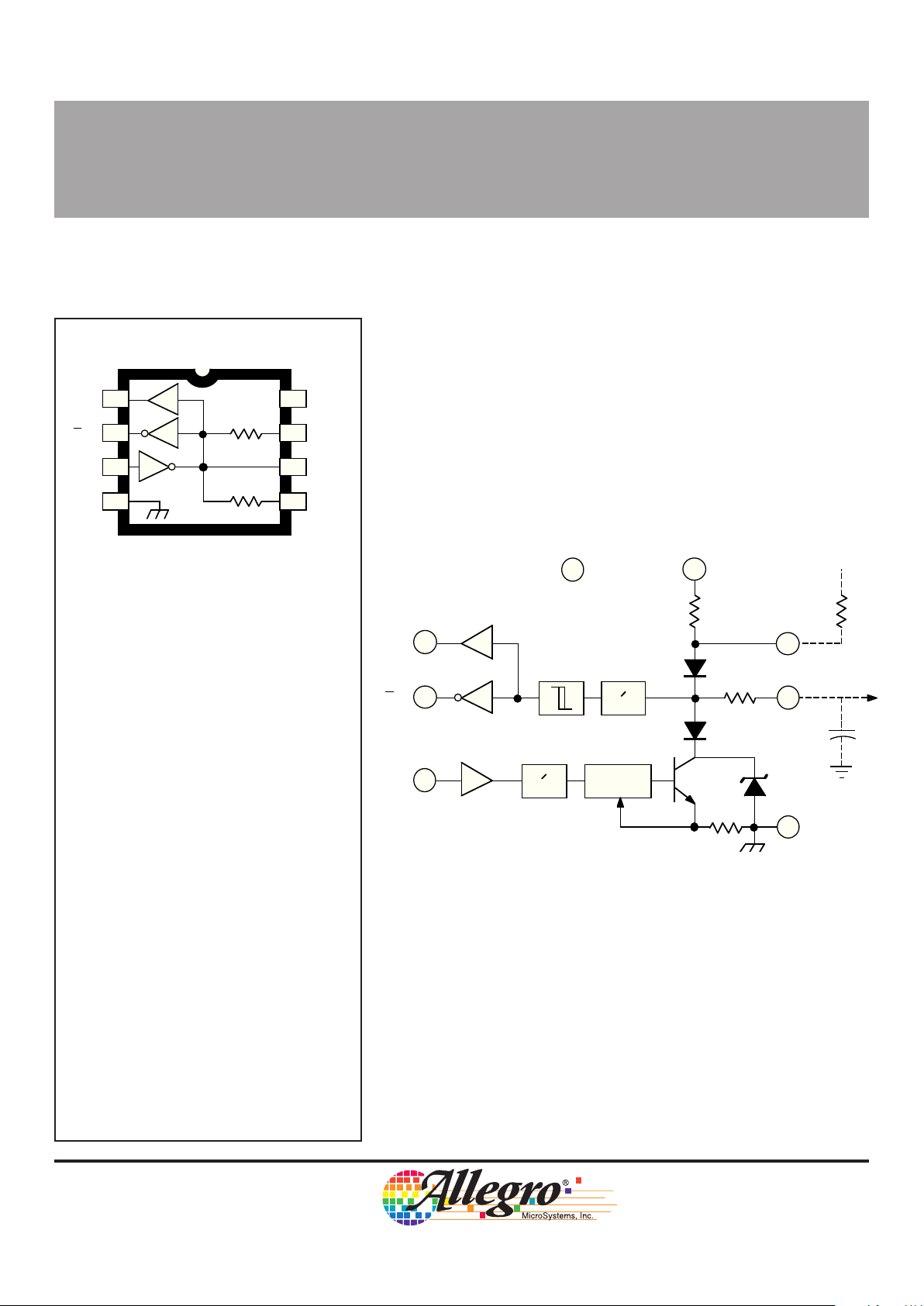
BUS DRIVER / RECEIVER
FUNCTIONAL BLOCK DIAGRAM
Rd
Rd
Td
GND
V
CC VS
REXT
BUS
6
5
4
7
2
1
3
8
CURRENT
LIMIT
22 kΩ
12 Ω
25 Ω
28 V
Data Sheet
27463
The ULQ2470L and ULQ2470M are bi-directional bus driver /
receivers designed specifically for automotive applications. They are
intended to be used as an interface between a microprocessor and a
single-wire multiplex data bus operating from the A-line or battery.
Each device consists of a wave-shaped open-collector driver, a pull-up
resistor, and an input filter and buffer.
Output driver protection circuitry provides output shutdown if
currents in excess of 25 to 30 mA occur. Additionally, over-voltage
shutdown occurs when the bus voltage exceeds approximately
22 volts.
Dwg. FP-039
FEATURES AND BENEFITS
■ Over-Voltage Protection
■ Diode Isolation from both Ground and Supply
■ Reverse-Battery Protection
■ Low Supply Current
■ High Noise Immunity
■ Output Current Limiting
■ Low Standby Current—24 mA Max.
■ Open-Ground Protection
■ Under-Voltage Lockout
2470
ULQ2470M
1
2
3
45
6
7
8
R
d
R
d
T
d
GND
V
CC
V
S
R
EXT
BUS
Dwg. PP-061
Note that the ULQ2470M (DIP) and the ULQ2470L
(SOIC) are electrically identical and share a
common terminal number assignment.
2470
BUS DRIVER / RECEIVER
115 Northeast Cutoff, Box 15036
Worcester, Massachusetts 01615-0036 (508) 853-5000
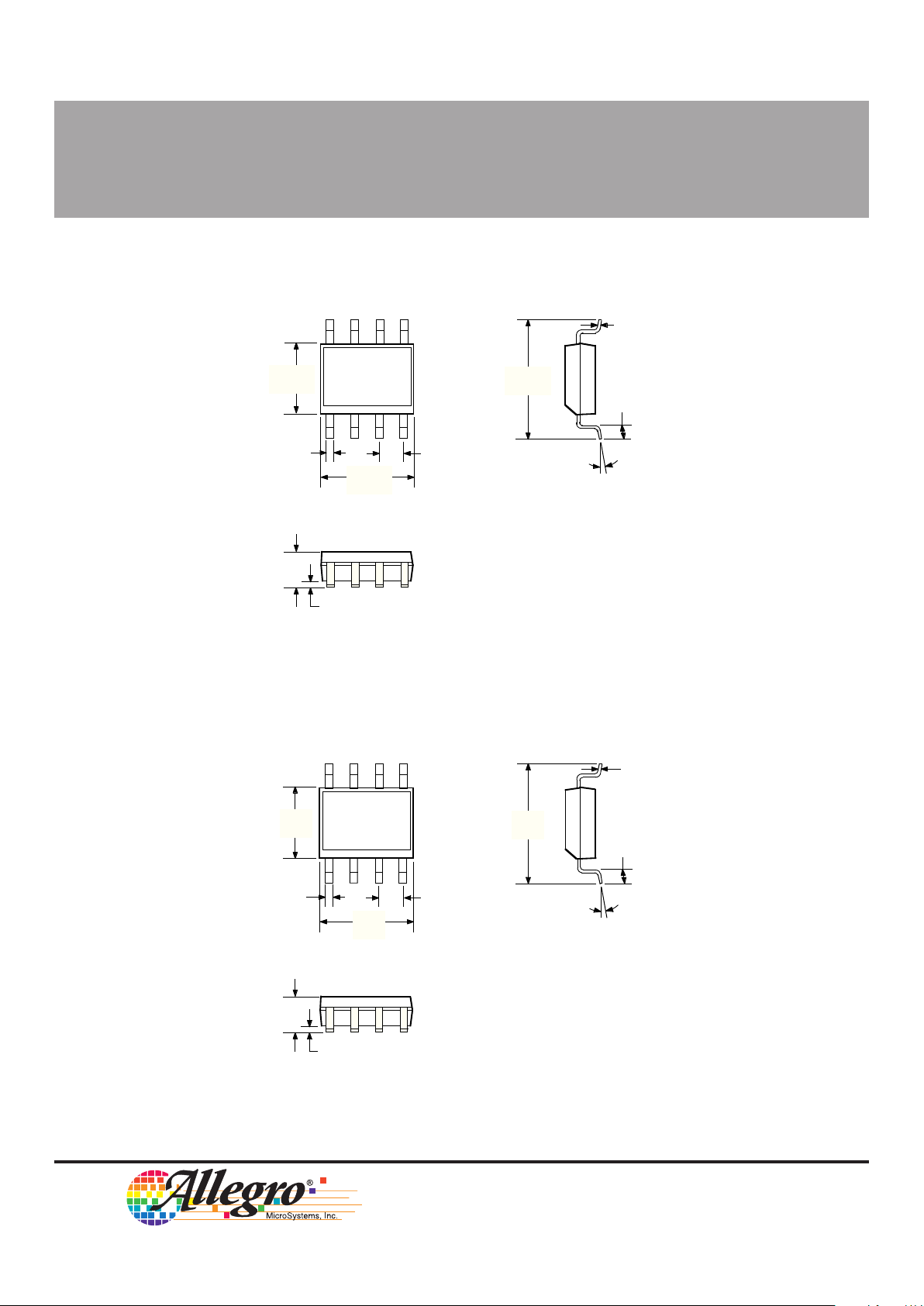
ULQ2470L
Dimensions in Inches
(for reference only)
Dimensions in Millimeters
(controlling dimensions)
0° TO 8°
0.1968
0.1890
0.2440
0.2284
0.050
0.016
Dwg. MA-007-8 in
0.050
BSC
0.0098
0.0075
8
1
0.1574
0.1497
0.020
0.013
0.0688
0.0532
0.0040 MIN.
Copyright © 1995, Allegro MicroSystems, Inc.
0° TO 8°
5.00
4.80
6.20
5.80
1.27
0.40
Dwg. MA-007-8 mm
1.27
BSC
0.25
0.19
8
1
4.00
3.80
0.51
0.33
1.75
1.35
0.10
MIN.
NOTES: 1. Lead spacing tolerance is non-cumulative.
2. Exact body and lead configuration at vendor’s option within limits shown.
 Loading...