

5881
BiMOS II DUAL
8-BIT LATCHED DRIVER
Data Sheet
26180.16
588 1
BiMOS II DUAL 8-BIT LATCHED
DRIVER WITH READ BACK
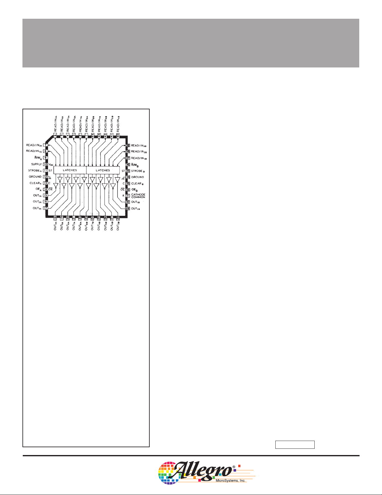
With 16 CMOS data latches (two sets of eight), CMOS control
circuitry for each set of latches, and a bipolar saturated driver for each
latch, the UCN5881EP provides low-power interface with maximum
flexibility. The driver includes thermal shutdown circuitry to protect
against damage from high junction temperatures and clamp diodes
for inductive load transient suppression.
The CMOS inputs cause minimal circuit loading and are compatible with standard CMOS, PMOS, and NMOS circuits. TTL or DTL
circuits may require the use of appropriate pull up resistors. When
reading back, each data input will sink 8 mA (if its corresponding latch
is low) or source 400 µA (if its corresponding latch is high). The read
back feature is for error checking. It allows the system to verify that
data has been received and latched.
The bipolar outputs are suitable for use with low-power relays,
solenoids, and stepping motors. The very-low output saturation
Dwg. No. A-14,225
voltage makes this device well-suited for driving LED arrays. The
output transistors are capable of sinking 50 mA and will maintain at
least 20 V in the OFF state. Outputs may be paralleled for higher
current capability.
The UCN5881EP dual 8-bit latched sink driver is rated for operation over the temperature range of -20°C to +85°C and is supplied in a
plastic 44-lead chip carrier conforming to the JEDEC MS-007AB
outline.
FEATURES
ABSOLUTE MAXIMUM RATINGS
Output Voltage, V
Output Sustaining Voltage, V
Output Current, I
Input Voltage Range,
V
. . . . . . . . . . . -0.3 V to VDD + 0.3 V
IN
Logic Supply Voltage, V
DISCONTINUED PRODUCT
Package Power Dissipation,
P
. . . . . . . . . . . . . . . . . . . See Graph
D
Operating Temperature Range,
T
. . . . . . . . . . . . . . . . -20°C to +85°C
A
Storage Temperature Range,
T
Caution: CMOS devices have input static
protection, but are susceptible to damage when
exposed to extremely high static electrical
charges.
— FOR REFERENCE ONLY
. . . . . . . . . . . . . . . -55°C to +150°C
S
. . . . . . . . . . . . . . 20 V
OUT
. . . . . . . . . . . . 50 mA
OUT
. . . . . . . . . . 15 V
DD
CE(sus)
.. . 15 V
■ 4.4 MHz Minimum Data-Input Rate
■ Low-Power CMOS Logic
■ 20 V, 50 mA (Max.) Outputs
■ Transient-Protected Outputs
■ Thermal Shutdown Protection
■ Low-Profile Leaded Chip Carrier
Always order by complete part number: UCN5881EP .
5881
BiMOS II DUAL
8-BIT LATCHED DRIVER
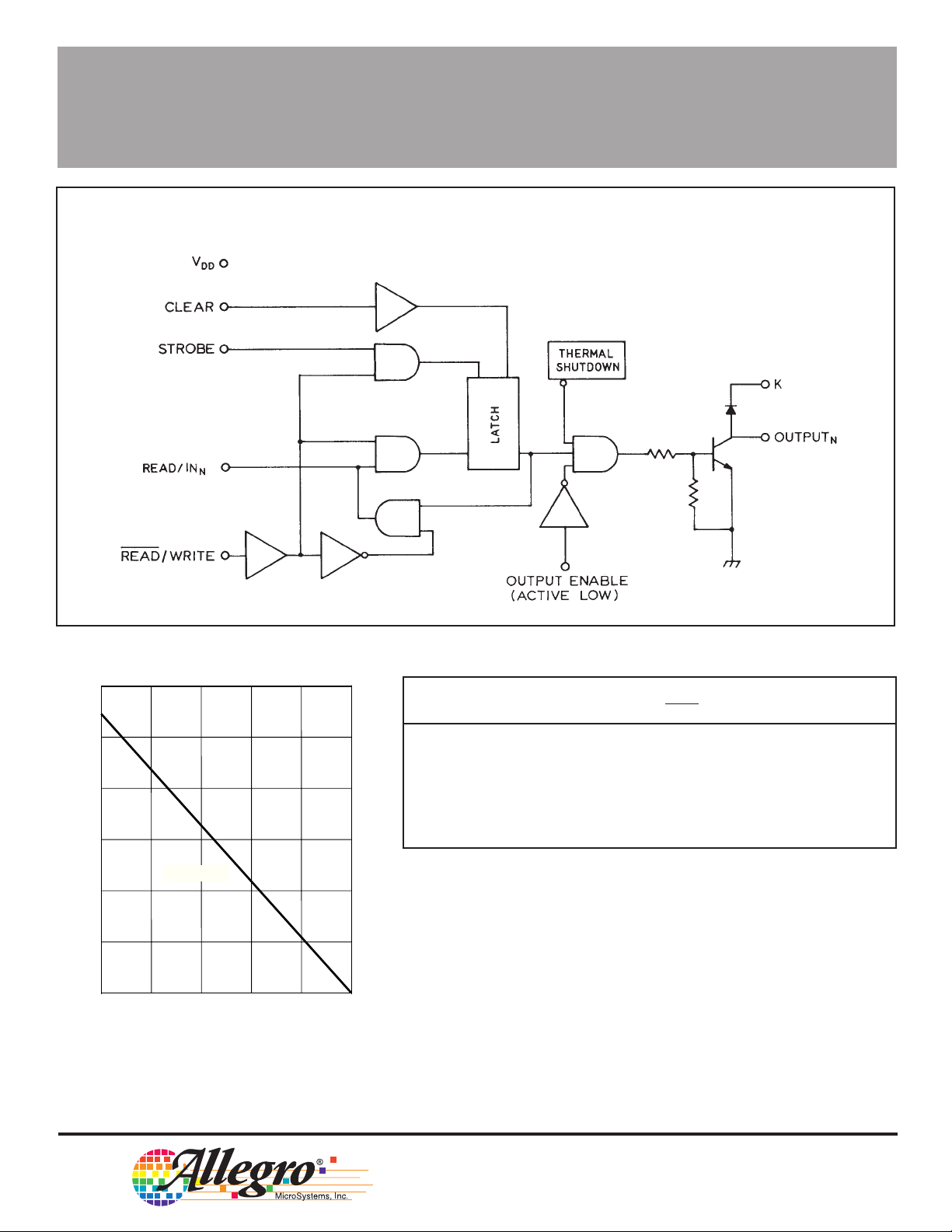
FUNCTIONAL BLOCK DIAGRAM
(1 of 16 Channels)
3.0
2.5
2.0
1.5
R = 46°C/W
θJA
1.0
0.5
ALLOWABLE PACKAGE POWER DISSIPATION IN WATTS
0
25
50 75 100 125 150
AMBIENT TEMPERATURE IN °C
Dwg. GP-025-1A
Dwg. No. A-14,227
TRUTH TABLE
Output Latch
Read/ln Strobe Clear Enable Read/Write Contents Output
X X X 1 X X OFF
0100 1 0 OFF
1100 1 1 ON
X 0 0 0 1 n-1 n-1
X X 1 X X 0 OFF
nX0X 0 n n
n = Present Latch Contents
n-1 = Previous Latch Contents
X = Irrelevant
115 Northeast Cutoff, Box 15036
Worcester, Massachusetts 01615-0036 (508) 853-5000
W
Copyright © 1985, 1995, Allegro MicroSystems, Inc.

5881
BiMOS II DUAL
8-BIT LATCHED DRIVER
ELECTRICAL CHARACTERISTICS at T
Characteristic Symbol Test Conditions Min. Max. Units
Output Leakage Current I
Output Saturation Voltage V
Output Sustaining Voltage V
Input Voltage V
Input Current I
Readback Output Voltage V
Logic Supply Current l
Clamp Diode Leakage Current I
Clamp Diode Forward Voltage V
CEX
CE(SAT)
CE(sus)
IN(0)
V
IN(1)
IN(0)
I
IN(1)
OUT(1)
V
OUT(0)
DD
R
F
= 25°C, V
A
V
I
OUT
I
OUT
I
OUT
VIN = 0.8 V — -10 µA
VIN = 5 V — 10 µA
I
OUT
I
OUT
All Drivers ON — 14 mA
All Drivers OFF — 3.0 mA
VR = 20 V — 50 µA
IF = 50 mA — 1.5 V
= 5 V (unless otherwise noted).
DD
Limits
= 20 V — 50 µA
OUT
= 10 mA — 0.1 V
= 25 mA — 0.5 V
= 25 mA, L = 2 mH 15 — V
-0.3 0.8 V
3.5 5.3 V
= -400 µA 3.5 — V
= 5.0 mA — 0.8 V
Dwg. No. A-14,228
TIMING CONDITIONS
(VDD = 5.0 V, Logic Levels are VDD and Ground)
A. Minimum Data Active Time Before Strobe Enabled
B. Minimum Data Active Time After Strobe Disabled
C. Minimum Strobe Pulse Width . . . . . . . . . . . . . . . . . . . . . . . . . . . . . . 125 ns
D. Typical Time Between Strobe Activation and Output
E. Typical Time Between Strobe Activation and Output
F. Minimum Clear Pulse Width . . . . . . . . . . . . . . . . . . . . . . . . . . . . . . . 225 ns
G. Minimum Data Pulse Width . . . . . . . . . . . . . . . . . . . . . . . . . . . . . . . 225 ns
(Data Set-Up Time) . . . . . . . . . . . . . . . . . . . . . . . . . . . . . . . . . . . 50 ns
(Data Hold Time) . . . . . . . . . . . . . . . . . . . . . . . . . . . . . . . . . . . . . 50 ns
ON to OFF Transition . . . . . . . . . . . . . . . . . . . . . . . . . . . . . . . . . . 5
OFF to ON Transition . . . . . . . . . . . . . . . . . . . . . . . . . . . . . . . . 500 ns
µs
A high on the READ/WRITE input allows
the circuit to accept data in. Information then
present at an input is transferred to its latch
when the STROBE is high. A high CLEAR
input will set all latches to the output OFF
condition regardless of the data or STROBE
input levels. A high OUTPUT ENABLE will
set all outputs to the OFF condition regardless of any other input conditions. When the
OUTPUT ENABLE is low, the outputs depend on the state of their respective latches.
A low on the READ/WRITE input will
allow the latched data to be read back on the
data input lines. Allow a minimum of 750 ns
delay (will increase with capacitive loading)
before reading back the state of the latches.
The read back feature is for error checking
applications and allows the system to verify
that data has been received and latched.

5881
BiMOS II DUAL
8-BIT LATCHED DRIVER
Dimensions in Inches
(controlling dimensions)
28
18
0.319
0.291
0.319
0.291
8.10
7.39
0.021
0.013
0.050
BSC
0.020
MIN
0.180
0.165
29
0.032
0.026
0.695
0.685
0.656
0.650
39
40
Dimensions in Millimeters
(for reference only)
28
29
0.812
0.661
0.656
0.650
144
0.695
0.685
INDEX AREA
2
17
7
6
Dwg. MA-005-44A in
18
17
0.533
0.331
8.10
7.39
1.27
BSC
0.51
MIN
4.57
4.20
NOTES: 1. Exact body and lead configuration at
vendor’s option within limits shown.
2. Lead spacing tolerance is non-cumulative.
17.65
17.40
16.662
16.510
INDEX AREA
39
144
17.65
17.40
2
6
40
16.662
16.510
7
Dwg. MA-005-44A mm
Allegro MicroSystems, Inc. reserves the right to make, from time to time, such departures from
the detail specifications as may be required to permit improvements in the design of its products.
The information included herein is believed to be accurate and reliable. However, Allegro
MicroSystems, Inc. assumes no responsibility for its use; nor for any infringements of patents or
other rights of third parties which may result from its use.
115 Northeast Cutoff, Box 15036
Worcester, Massachusetts 01615-0036 (508) 853-5000
 Loading...