

8182
PRELIMINARY INFORMATION DATA SHEET
LOW-DROPOUT,
(Subject to change without notice)
3 V REGULATOR
November 14, 1994
Data Sheet
27468.2
8182
LOW-DROPOUT, 3 V REGULATOR
— HIGH EFFICIENCY
Designed specifically to meet the requirement for extended operation of battery-powered equipment such as cordless and cellular
telephones, the A8182SL voltage regulator offers the reduced dropout
voltage and quiescent current essential for maximum battery life.
Applicable also to palmtop computers and personal data assistants, the
device delivers a regulated 3 V output at up to 150 mA.
A PMOS pass element provides a typical dropout voltage of only
85 mV at 60 mA of load current. The low dropout voltage permits
deeper battery discharge before output regulation is lost. Furthermore,
quiescent current does not increase as the dropout voltage is
approached, an ideal feature in standby/resume power systems where
data integrity is crucial. Regulator accuracy and excellent temperature
characteristics are provided by a bandgap reference. An ENABLE input
and RESET output gives the designer complete control over power up,
standby, or power down.
This device is supplied in an 8-lead small-outline plastic package
(SOIC) for surface-mount applications. The A8182SL is rated for
operation over a temperature range of -20°C to +85°C.
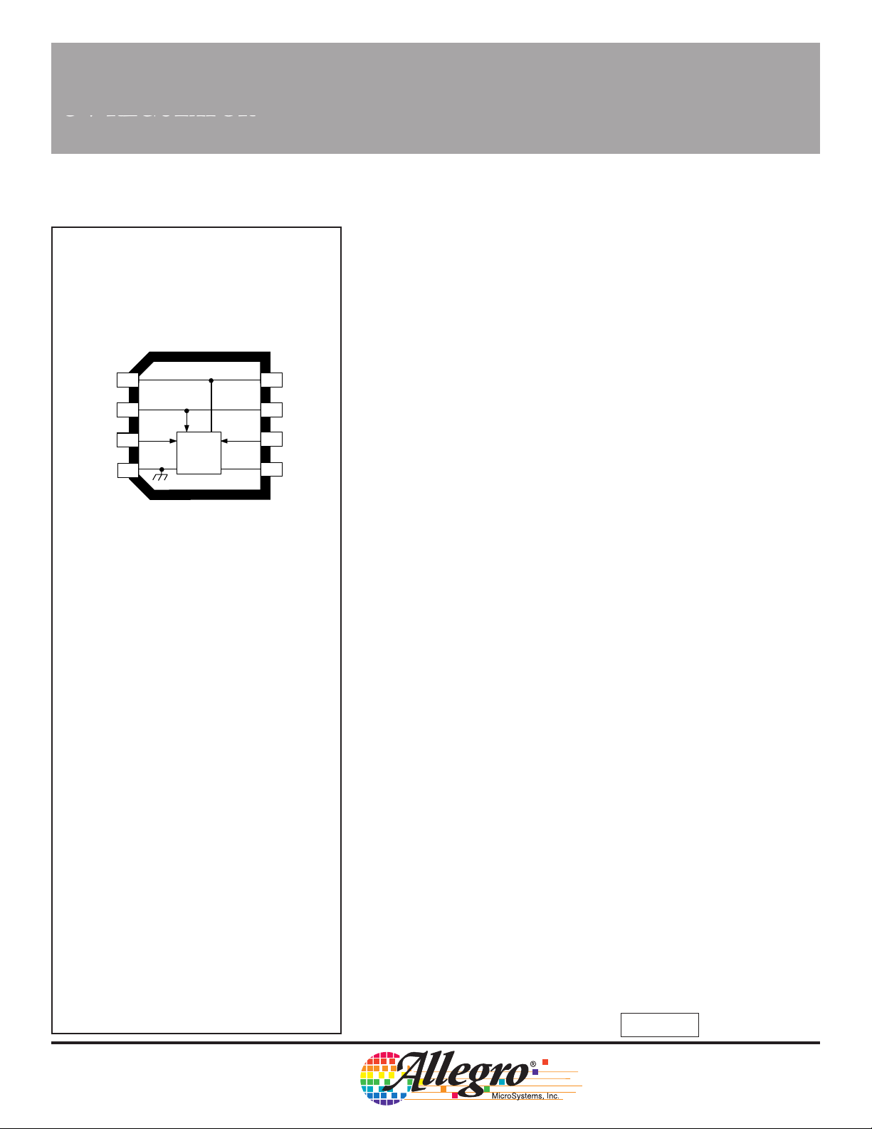
OUT
ENABLE
GND
1
IN
2
3
4
3 V
VR
8
OUT
7
IN
6
COMP
RESET
5
Dwg. PS-020
FEATURES AND BENEFITS
ABSOLUTE MAXIMUM RATINGS
Input Voltage, VI. . . . . . . . . . . . . . 10 V
Output Current, IO. . . . . . . . . 150 mA*
Enable Input Voltage, VE. . . . . . . . . . V
Reset Output Voltage, VOR. . . . . . . . V
Reset Output Current, IOR. . . . 1.0 mA
Operating Temperature Range,
TA. . . . . . . . . . . . . -20°C to +85°C
DISCONTINUED PRODUCT
Junction Temperature, TJ. . . +150°C
Storage Temperature Range,
TS. . . . . . . . . . . . -40°C to +150°C
— FOR REFERENCE ONLY
* Output current rating is limited by input voltage,
duty cycle, and ambient temperature. Under any
set of conditions, do not exceed a junction temperature of +150°C. See next page.
† Fault conditions that produce excessive junction
temperature will activate device thermal shutdown
circuitry. These conditions can be tolerated but
should be avoided.
I
I
†
■ High Efficiency Provides Extended Battery Life
■ 85 mV Typical Dropout Voltage at IO = 60 mA
■ 46 µA Typical Quiescent Current at VI = 6 V
Less than 1 µA “Sleep” Current
■ Up to 150 mA Output Current
■ CMOS-Compatible ON/OFF Control
For Power-Up, Standby, or Shutdown
■ Internal Thermal Protection
■ Surface-Mount Package
APPLICATIONS
■ Cordless and Cellular Telephones
■ Personal Data Assistants
■ Personal Communicators
■ Palmtop Computers
Always order by complete part number: A8182SL .
8182
72813
5
4
6
LOW-DROPOUT,
3 V REGULATOR
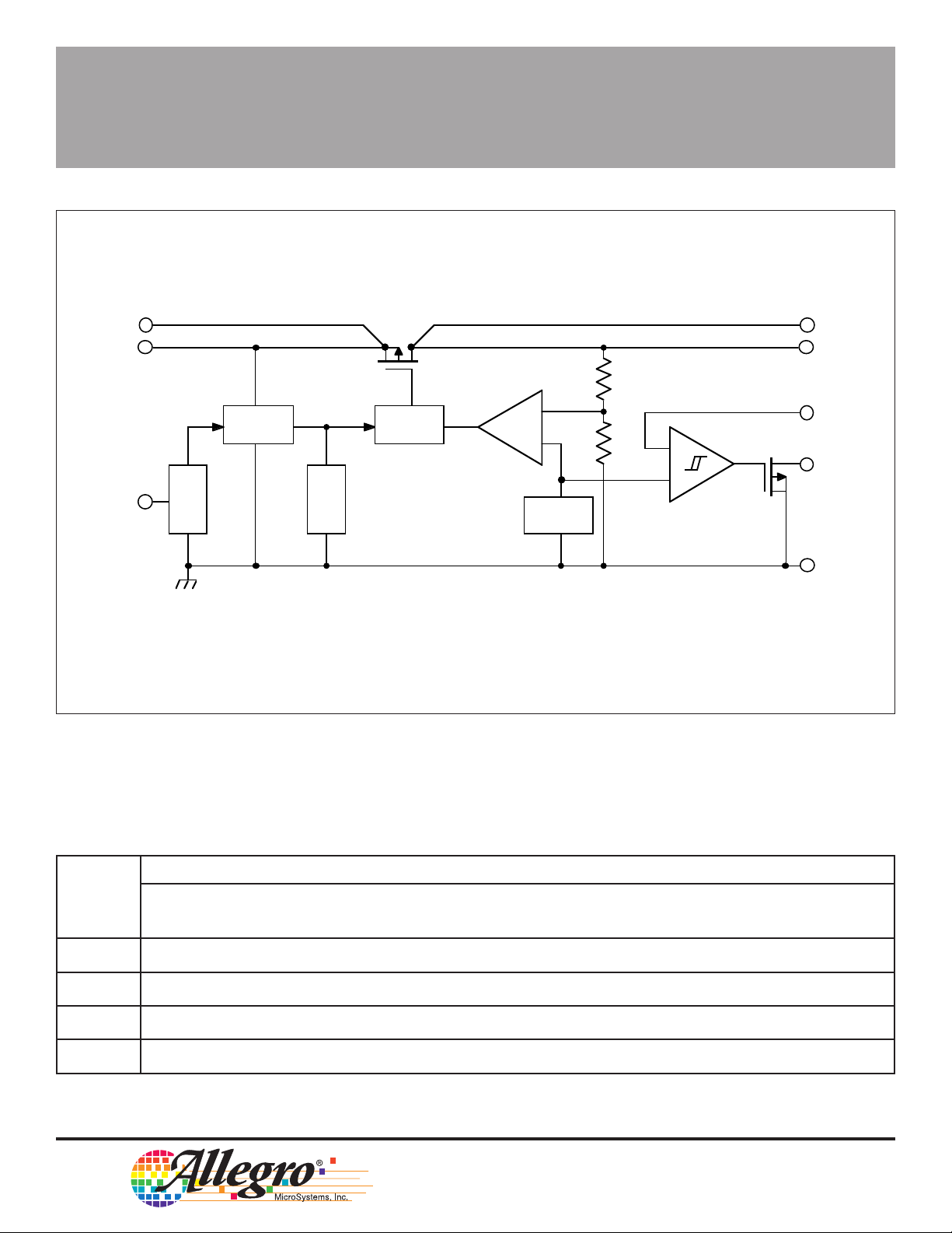
FUNCTIONAL BLOCK DIAGRAM
IN
IN
ERROR
AMP
BANDGAP
REF.
ENABLE
ENABLE
BIAS
THERMAL
PROTECT.
DRIVE
For proper operation, terminals 1 and 8 should be externally connected together,
terminals 2 and 7 should be externally connected together.
1.23 V
OUT
OUT
COMP
–
RESET
+
GND
Dwg. FS-012-2
MAXIMUM ALLOWABLE OUTPUT CURRENT with device mounted on 2.24" x 2.24"
(56.9 mm x 56.9 mm) solder-coated copper-clad board in still air.
Maximum Allowable Output Current in Milliamperes with VI = 8 V, TJ = 150°C, Period ≤10 s*
dc (Duty Cycle)
T
A
25°C 150 150 150 150 150 150 150 150 150
50°C 150 150 150 150 150 150 150 150 150
70°C 145 150 150 150 150 150 150 150 150
85°C 120 130 150 150 150 150 150 150 150
*IO = (TJ - TA)/([VI - VO] R
Output current rating can be increased (to 150 mA maximum) by heat sinking or reducing the input voltage. Conditions that produce excessive
junction temperature will activate device thermal shutdown circuitry. These conditions can be tolerated but should be avoided.
100% 90% 80% 70% 60% 50% 40% 30% 20%
• dc) = (150 - TA)/(5 • 108 • dc)
θJA
115 Northeast Cutoff, Box 15036
Worcester, Massachusetts 01615-0036 (508) 853-5000
W
Copyright © 1994 Allegro MicroSystems, Inc.
8182
LOW-DROPOUT,
3 V REGULATOR
ELECTRICAL CHARACTERISTICS at T
= +25°C (unless otherwise noted).
A
Limits
Characteristic Symbol Test Conditions Min. Typ. Max. Units
Output Voltage V
Output Volt. Temp. Coeff. α
Line Regulation ∆V
Load Regulation ∆V
O
VO
O(∆VI)
O(∆IO)
4 V ≤ VI ≤ 8 V, TA = +25°C 2.95 3.00 3.05 V
10 µA ≤ I
= 3 V, IO = 60 mA, -20°C ≤ TA ≤ +85°C 2.70 — — V
V
I
≤ 100 mA -20°C ≤ TA ≤ +85°C 2.90 3.00 3.10 V
O
VI = 6 V, IO = 10 mA — — ±0.5 mV/°C
6 V ≤ VI ≤ 8 V, IO = 1 mA — 7.0 14 mV
4 V ≤ V
≤ 6 V, IO = 1 mA — 5.5 11 mV
I
1 mA ≤ IO ≤ 100 mA, VI = 8 V — 12 30 mV
1 mA ≤ I
1 mA ≤ I
≤ 100 mA, VI = 6 V — 11 25 mV
O
≤ 100 mA, VI = 4 V — 8.0 20 mV
O
Dropout Voltage VImin - VOIO = 60 mA — 85 150 mV
= 125 mA* — 175 TBD mV
I
O
Quiescent Current I
Q
VI = 6 V, 1 mA ≤ IO ≤ 100 mA, VE ≥ 2.0 V — 46 60 µA
(GND terminal current) VI = 8 V, 1 mA ≤ IO ≤ 100 mA, VE ≥ 2.0 V — 50 65 µA
I
ENABLE Input Voltage V
ENABLE Input Current I
COMP Threshold Voltage V
COMP Threshold Volt. TC α
COMP Threshold Hys. V
COMP Input Current I
COMP Input Current TC α
RESET Leakage Current I
RESET Output Voltage V
Thermal Shutdown Temp. T
Thermal Resistance R
Q(off)
EH
V
EL
E
C(t)
VC
C(hys)
C
IC
OR
OR
J
θJA
4 V ≤ VI ≤ 8 V, VE ≤ 0.8 V — 0.05 1.0 µA
4 V ≤ VI ≤ 8 V, Output ON 2.0 — — V
-20°C ≤ TA ≤ +85°C Output OFF — — 0.8 V
TA ≤ +85°C, VE = VI = 8 V — — ±0.1 µA
4 V ≤ VI ≤ 8 V, VC increasing from 0 1.20 1.23 1.30 V
4 V ≤ VI ≤ 8 V — — ±0.5 mV/°C
4 V ≤ VI ≤ 8 V 12 34 50 mV
0 V ≤ VC ≤ V
O
4 V ≤ VI ≤ 8 V — -0.5 -2.5 nA/°C
VOR = VI = 10 V, TA = +85°C — — 2.0 µA
IOR = 500 µA — 100 400 mV
Mounted on 2.24" x 2.24" solder-coated — 108 — °C/W
copper-clad board in still air
Typical values are at TA = +25°C and are given for circuit design information only.
* Pulse test (≤50 ms). See previous page for duty cycle limitations.
— -25 TBD nA
150 — — °C

8182
LOW-DROPOUT,
3 V REGULATOR
LOAD REGULATION LINE REGULATION
TYPICAL CHARACTERISTICS
3.06
3.04
3.02
3.00
2.98
2.96
OUTPUT VOLTAGE in VOLTS
2.94
2.92
3.06
T = -20°C
A
1 V INTERVALS
0
25 50 100 15075
OUTPUT CURRENT in mA
V = 4 V
I
V = 8 V
I
125
Dwg. GP-052
3.06
3.04
3.02
3.00
2.98
2.96
OUTPUT VOLTAGE in VOLTS
2.94
2.92
2.0
3.06
3.0 4.0 6.0 8.05.0
INPUT VOLTAGE in VOLTS
I = 100 mA
O
T = -20°C
A
50 mA INTERVALS
I = 0 mA
O
7.0
Dwg. GP-053
T = 25°C
3.04
3.02
3.00
2.98
2.96
OUTPUT VOLTAGE in VOLTS
2.94
2.92
T = 25°C
A
1 V INTERVALS
0
25 50 100 15075
OUTPUT CURRENT in mA
V = 4 V
I
V = 8 V
I
125
Dwg. GP-052-1
3.04
3.02
3.00
I = 100 mA
2.98
2.96
OUTPUT VOLTAGE in VOLTS
2.94
2.92
2.0
O
3.0 4.0 6.0 8.05.0
INPUT VOLTAGE in VOLTS
A
50 mA INTERVALS
I = 0 mA
O
7.0
Dwg. GP-053-1
CAUTION: Maximum allowable duty cycle will be significantly less than 100% at high temperatures, at high input voltages, or at high output currents.
See Maximum Allowable Output Current table.
115 Northeast Cutoff, Box 15036
Worcester, Massachusetts 01615-0036 (508) 853-5000

8182
A
LOW-DROPOUT,
3 V REGULATOR
LOAD REGULATION LINE REGULATION
TYPICAL CHARACTERISTICS (cont’d)
3.06
3.04
3.02
3.00
2.98
2.96
OUTPUT VOLTAGE in VOLTS
2.94
2.92
3.5
T = 85°C
A
1 V INTERVALS
0
25 50 100 15075
OUTPUT CURRENT in mA
3.06
3.04
V = 4 V
I
V = 8 V
I
125
Dwg. GP-052-2
3.02
3.00
2.98
2.96
OUTPUT VOLTAGE in VOLTS
2.94
2.92
OUTPUT VOLTAGE
2.0
I = 100 mA
O
3.0 4.0 6.0 8.05.0
INPUT VOLTAGE in VOLTS
T = 85°C
A
50 mA INTERVALS
I = 0 mA
O
7.0
Dwg. GP-053-2
3.0
V = 6 V
2.5
2.0
1.5
1.0
OUTPUT VOLTAGE in VOLTS
0.5
0
UNDEFINED
1.0
INPUT VOLTAGE in VOLTS
0
2.0
I = 10 µA - 100 m
O
T = 25°C
A
3.0
Dwg. GP-056-1
4.0
3.01
3.00
2.99
2.98
OUTPUT VOLTAGE in VOLTS
-50
AMBIENT TEMPERATURE in °C
0 +50
I
I = 10 mA
O
+100
Dwg. GP-050
CAUTION: Maximum allowable duty cycle will be significantly less than 100% at high temperatures, at high input voltages, or at high output currents.
See Maximum Allowable Output Current table.

8182
A
LOW-DROPOUT,
3 V REGULATOR
QUIESCENT (GROUND TERMINAL) CURRENT
50
V = 6 V
I
I = 10 mA
48
46
44
O
V ≥ 2 V
E
TYPICAL CHARACTERISTICS (cont’d)
60
I = 1 – 100 m
O
50
40
T = -20°C
A
30
20
10
T = 25°C
A
T = 85°C
A
QUIESCENT (GROUND TERMINAL) CURRENT in µA
-50
0 +50
AMBIENT TEMPERATURE in °C
COMPARATOR VOLTAGE
+V
RESET OUTPUT VOLTAGE in VOLTS
0
1.22
COMPARATOR INPUT VOLTAGE in VOLTS
1.24
A
A
T = 25°C
T = -20°C
1.26 1.28
A
T = 85°C
Dwg. GP-051
V = 6 V
I
I = 10 mA
O
Dwg. GP-057
+100
0
QUIESCENT (GROUND TERMINAL) CURRENT in µA
0
2.0
INPUT VOLTAGE in VOLTS
DROPOUT VOLTAGE
0.25
0.20
T = 85°C
A
T = 25°C
A
T = -20°C
0.15
0.10
0.05
DROPOUT VOLTAGE in VOLTS
0
0
A
25 50 100 15075
OUTPUT CURRENT in mA
4.0
6.0
8.0
Dwg. GP-055
125
Dwg. GP-054
CAUTION: Maximum allowable duty cycle will be significantly less than 100% at high temperatures, at high input voltages, or at high output currents.
See Maximum Allowable Output Current table.
115 Northeast Cutoff, Box 15036
Worcester, Massachusetts 01615-0036 (508) 853-5000

8182
LOW-DROPOUT,
3 V REGULATOR
TYPICAL CHARACTERISTICS (concluded)
LOAD TRANSIENT PERFORMANCE ENABLE TRANSIENT PERFORMANCE
VI = 3.2 V to 6.2 V, CO = 1 µF, IO = 60 mA, TA = 25°CVI = 3.2 V to 6.2 V, CO = 1 µF, TA = 25°C
3.5 V
3.0 V
V
O
2.5 V
<100 µs
100 mA
I
O
1 mA
<300 µs
INPUT, COMPARATOR, & OUTPUT RELATIONSHIPS
The RESET output of the comparator produces a logic low whenever the COMP input is
below 1.23 V. An out-of-regulation detector can
be configured by dividing down the regulator
output (an R/R divider is typical) and connecting it
to the COMP input. As tne regulator input is
ramped up, the RESET signal becomes valid
(low) at approximately VI = 1.3 V. The RESET
signal will go high when VC = 1.23 V (VO = 2.46 V
with an R/R divider). Comparator hysteresis
prevents oscillations under low battery conditions.
The RESET open-drain output requires an
external pull-up resistor. This can be returned to
either the input supply or the regulator output,
depending on suystem requirements. Note that
the RESET sink current is adds to the battery
drain in a low-battery condition. Suggested
values range from 100 kΩ to 1 MΩ. RESET
should be left unconnected if it is not used.
Dwg. WP-026
V
I
V
O
V *
C
V
OR
3.0 V
V
O
0
V
E
V
0
1.3 V
3.0 V
1.23 V
I
OUTPUT UNDEFINED
V
C(hys)
<125 µs
10 V MAX.
<250 µs
Dwg. WP-025
*Comparator input voltage is normally obtained
from a resistive divider off of the output.
Dwg. WP-027

8182
LOW-DROPOUT,
3 V REGULATOR
Dimensions in Inches
(Based on 1 mm = 0.03937”)
8
0.0098
0.0075
0.1574
0.1497
0.020
0.013
0.0688
0.0532
1
0.0040
0.1968
0.1890
MIN.
0.050
BSC
Dimensions in Millimeters
8
4.00
3.80
0.2440
0.2284
6.20
5.80
0° TO 8°
0.050
0.016
Dwg. MA-007-8 in
0.25
0.19
1.27
0.40
Allegro MicroSystems, Inc. reserves the right to make, from
time to time, such departures from the detail specifications as
may be required to permit improvements in the design of its
products. Components made under military approvals will be in
accordance with the approval requirements.
The information included herein is believed to be accurate
and reliable. However, Allegro MicroSystems, Inc. assumes no
responsibility for its use; nor for any infringements of patents or
other rights of third parties which may result from its use.
0.51
0.33
1.75
1.35
1
0.10 MIN.
5.00
4.80
1.27
BSC
0° TO 8°
Dwg. MA-007-8 mm
NOTES: 1. Lead spacing tolerance is non-cumulative.
2. Exact body and lead configuration at vendor’s option within limits shown.
115 Northeast Cutoff, Box 15036
Worcester, Massachusetts 01615-0036 (508) 853-5000
 Loading...