

Page 1
8178
Data Sheet
27468.22
PRODUCT PREVIEW
(Subject to change without notice)
April 5, 1996
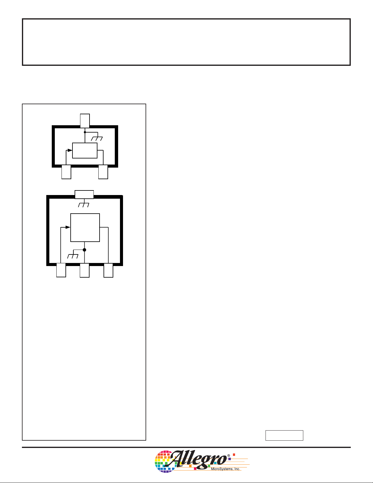
3
VR
7.7 V
1
VR
2
7.7 V
LOW-DROPOUT,
7.7 V PREREGULATOR
Designed specifically to meet the stringent requirements of automotive applications, the A8178LLR and A8178LLT provide an output
voltage of 7.7 V ±15% for supply voltages greater than 6.9 V. They
also provide a low-dropout tracking output for supply voltages down to
2.5 V. These regulators are intended to be used with sensitive automotive electronics systems that do not have the capability of low dropout
operation and cannot withstand the high-voltage transients typical of
automotive applications. These 7.7 V preregulators will withstand all
ISO pulses (ignition coil disconnect requires an external diode) and will
continue to operate during positive power supply transients (noise).
These devices are supplied in small-outline plastic transistor
packages for surface-mount applications. The A8178LLR is supplied in
the minimum footprint SOT-23/TO-236AB; the A8178LLT is furnished in
the SOT-89/TO-243AA for increased allowable package power dissipation.
2 31
Dwg. PD-0xx
ABSOLUTE MAXIMUM RATINGS
Input Voltage, VI. . . . . . . . . . . . . . 30 V
Reverse Input Voltage, VRI. . . . -120 V
Output Current, IO. . . . . . . . . . . . TBD*
Operating Temperature Range,
TA. . . . . . . . . . . . -40°C to +150°C
Junction Temperature, TJ. . . . +150°C
Storage Temperature Range,
TS. . . . . . . . . . . . -40°C to +170°C
* Output current rating is limited by input voltage,
duty cycle, and ambient temperature. Under
any set of conditions, do not exceed a junction
temperature of +150°C. See next page.
T
his document contains information on a product under development. Allegro
MicroSystems, Inc. reserves the right to change or discontinue this product without
notice.
Always order by complete part number: A8178LLT .
Page 2
8178
LOW-DROPOUT,
7.7 V PREREGULATOR
ELECTRICAL CHARACTERISTICS over operating temperature range.
Limits
Characteristic Symbol Test Conditions Min. Typ. Max. Units
Output Voltage V
Output Volt. Temp. Coeff. α
Line Regulation ∆V
Load Regulation ∆V
Quiescent Current I
Power Dissipation P
Thermal Resistance* R
O
VO
O(∆VI)
O(∆IO)
Q
d
θJA
6.9 V ≤ VI ≤ 24 V 6.5 7.7 8.8 V
2.5 V ≤ V
V
= 120 V, pulse test — — 11 V
I
≤ 6.9 V VI - 0.4 — — V
I
VI = 13.5 V, IO = 0 — — 2.5 mA
2.5 V ≤ V
≤ 8 V, IO = 0 — — 5.6 mA
I
VI = 13.5 V, IO = 15 mA — — 130 mW
A8178LLR — 575 — °C/W
A8178LLT — 200 — °C/W
Typical values are at T
*Mounted on 2.24" x 2.24" solder-coated copper-clad board in still air.
= +25°C and are given for circuit design information only.
A
— — TBD mV/°C
— — TBD mV
— — TBD mV
INTERNAL PROTECTIVE FEATURES
ISO
Pulse No. Test Test Conditions (at T
1 Inductive Turn Off (Negative) V
2 Inductive Turn Off (Positive) V
3a Capacitive/Inductive Coupling (Neg) V
3b Capacitive/Inductive Coupling (Pos) V
4 Reverse Battery V
5 Load Dump V
6 Ignition Coil Disconnect V
EXTERNAL PROTECTION REQ’D
7 Field Decay (Negative) V
115 Northeast Cutoff, Box 15036
Worcester, Massachusetts 01615-0036 (508) 853-5000
Copyright © 1996 Allegro MicroSystems, Inc.
= -100 V, RS = 10 Ω, tr = 1 µs, td = 2 ms
S
= 100 V, RS = 10 Ω, tr = 1 µs, td = 50 µs, non-operating
S
= -150 V, RS = 50 Ω, tr = 50 ns, td = 100 ns
S
= 100 V, RS = 50 Ω, tr = 50 ns, td = 100 ns
S
= -14 V, td = 20 s, non-operating
S
= 86.5 V, RS = 0.5 Ω, tr = 5 ms, td = 400 ms
S
= -300 V, RS = 30 Ω, tr = 60 µs, td = 300 µs
S
= -80 V, RS = 10 Ω, tr = 5 ms, td = 100 ms
S
= +25°C)
A
Page 3

8178
LOW-DROPOUT,
7.7 V PREREGULATOR
A8178LLR
Dimensions in Inches
(for reference only)
0.055
0.047
0.024
0.018
0.004
0.0005
0.020
0.015
0.120
0.110
3
1
2
0.1039
0.083
0.040
0.080
0.035
0.070
Dimensions in Millimeters
(controlling dimensions)
0.044
0.035
0.007
0.003
0.027
REF
Dwg. MA-010 in
3.04
2.80
0.51
0.37
1.40
1.20
1
0.60
0.45
2.05
1.78
0.10
0.013
NOTES: 1. Lead spacing tolerance is non-cumulative.
2.Exact body and lead configuration at vendor’s option within limits shown.
1.12
0.89
0.18
0.085
3
2.64
2
2.10
0.69
REF
1.03
0.89
Dwg. MA-010 mm
Page 4

8178
LOW-DROPOUT,
7.7 V PREREGULATOR
A8178LLT
Dimensions in Inches
(for reference only)
0.155
0.167
0.035
0.047
0.059
BSC
1
0.173
0.181
0.064
0.072
0.090
23
0.102
0.014
0.019
0.017
0.022
0.118
BSC
Dimensions in Millimeters
(controlling dimensions)
4.40
4.60
1.62
1.83
0.055
0.063
0.014
0.017
0.084
0.090
Dwg. MA-009-3 in
1.40
1.60
0.35
0.44
3.94
4.25
1
23
0.89
1.20
1.50
BSC
3.00
BSC
NOTES: 1. Lead spacing tolerance is non-cumulative.
2.Exact body and lead configuration at vendor’s
option within limits shown.
2.29
2.60
2.13
2.29
0.36
0.48
0.44
0.56
Dwg. MA-009-3 mm
Allegro MicroSystems, Inc. reserves the right to make, from time to time, such
departures from the detail specifications as may be required to permit improvements
in the design of its products.
The information included herein is believed to be accurate and reliable.
However, Allegro MicroSystems, Inc. assumes no responsibility for its use; nor for
any infringements of patents or other rights of third parties which may result from its
use.
115 Northeast Cutoff, Box 15036
Worcester, Massachusetts 01615-0036 (508) 853-5000
 Loading...