

Allegro A3425LK-TK, A3425LK Datasheet
The A3425LK dual Hall-effect switch is an extremely
temperature-stable and stress-resistant sensor especially suited for use in
digital-encoder systems in the harsh environments of automotive or
industrial applications over extended temperature ranges to +150°C.
Superior high-temperature performance is made possible through
dynamic offset cancellation, which reduces the residual offset voltage
normally caused by device overmolding, temperature dependencies, and
thermal stress. This device also eliminates the major manufacturing
hurdles encountered in fine-pitch direction-detection applications,
namely maintaining accurate mechanical location between the two active
Hall elements. Here, the two Hall elements are photolithographically
aligned to better than 1 µm, as contrasted with 100 µm or worse mechanical location tolerance when manufactured discretely. The
A3425LK is an ultra-sensitive device optimized for use with highdensity ring magnets.
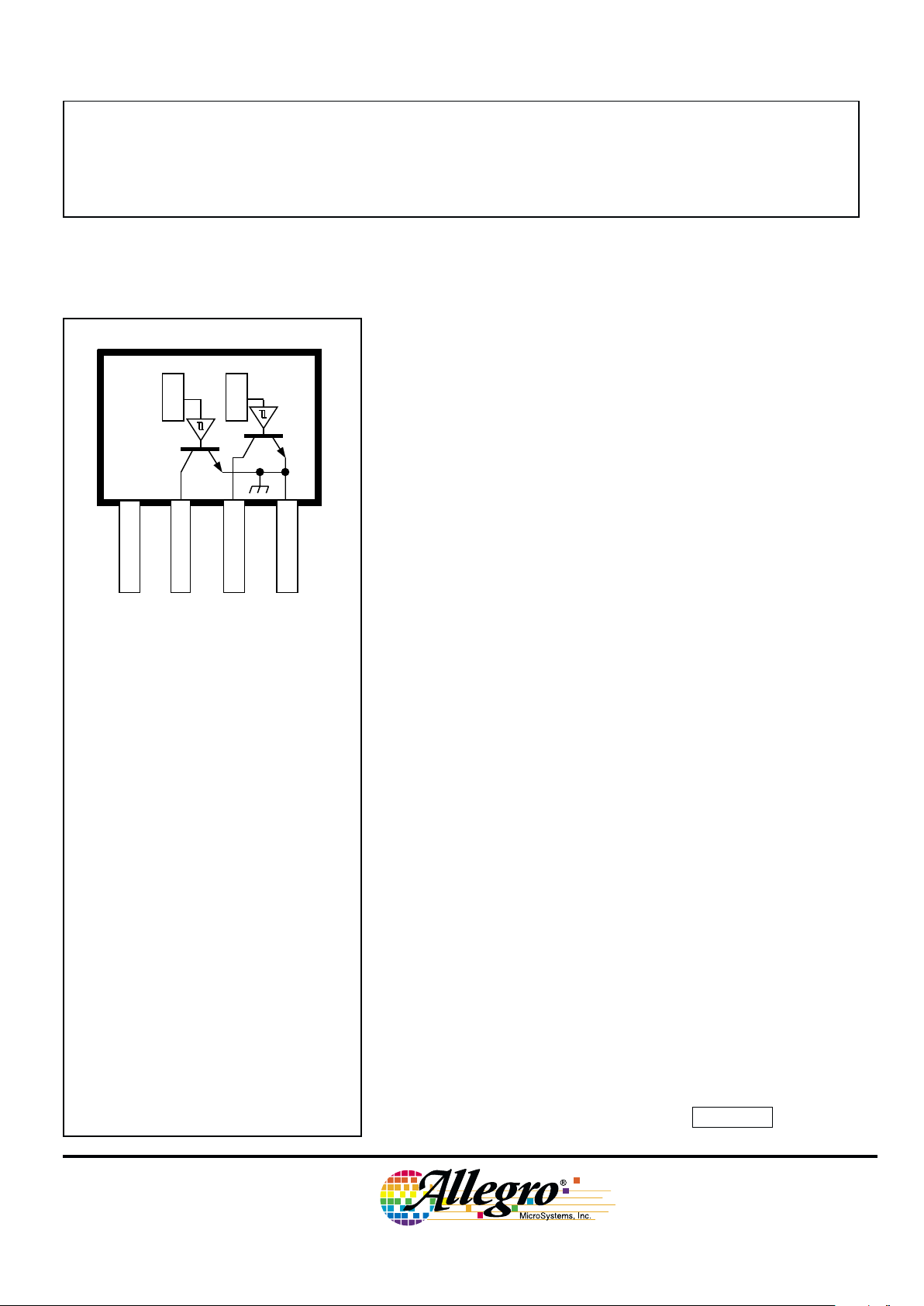
The device includes on a single silicon chip a voltage regulator, two
independent chopper-stabilized Hall-voltage generators , two smallsignal amplifiers, two Schmitt triggers, and two short-circuit protected
open-collector outputs to sink up to 30 mA each. An on-board regulator
permits operation with supply voltages of 3.3 to 26.5 volts. With
suitable output pull ups, it can be used directly with bipolar or MOS
logic circuits.
The A3425LK dual Hall-effect switch is supplied in a 4-pin plastic
SIP for operation over a temperature range of -40°C to +150°C. A
similar device, with on-chip logic processing specifically for direction
detection applications, in a 5-pin SIP, is the A3422LKA.
FEATURES
■ Two Matched Hall Switches On A Single Substrate
■ 1 mm Sensor-to-Sensor Spacing
■ Superior Temperature Stability
■ Resistant to Physical Stress
■ Output Short-Circuit Protection
■ Operation From Unregulated Supply
■ Reverse Battery Protection
■ Solid-State Reliability
■ Integrated ESD Protection on Outputs and Supply
Data Sheet
27651.20
PRELIMINARY INFORMATION
(subject to change without notice)
August 21, 2000
Pinning is shown viewed from branded side.
DUAL, CHOPPER-STABILIZED, ULTRA-SENSITIVE,
BIPOLAR HALL-EFFECT SWITCH
3425
ABSOLUTE MAXIMUM RATINGS
at TA = +25°C
Supply Voltage, VCC........................ 26.5 V
Reverse Battery Voltage, V
RCC
.......... -18 V
Zener Current, IZ............................ 100 mA
Magnetic Flux Density, B ........... Unlimited
Output Off Voltage, V
OUT
.................... V
CC
Output Current, I
OUT
........................ 30 mA
Reverse Output Current, I
OUT
........ -50 mA
Package Power Dissipation, PD. See Graph
Junction Temperature, TJ............... +170°C
Operating Temperature Range,
TA, ............................ -40°C to +150°C
Storage Temperature Range,
TS.............................. -65°C to +170°C
Always order by complete part number, e.g., A3425LK .
Dwg. PH-017
1
SUPPLY
V
CC
4
GROUND
32
X
OUTPUT
2
OUTPUT
1
X
3425
DUAL, CHOPPER-STABILIZED,
ULTRA-SENSITIVE,
BIPOLAR HALL-EFFECT SWITCH
115 Northeast Cutoff, Box 15036
Worcester, Massachusetts 01615-0036 (508) 853-5000
2
FUNCTIONAL BLOCK DIAGRAM
Copyright © 2000, Allegro MicroSystems, Inc.
OUTPUT
1
<1Ω
X
DYNAMIC
OFFSET CANCELLATION
REG.
TO ALL
SUBCIRCUITS
SUPPLY
CONTROL
CURRENT
LIMIT
SAMPLE
& HOLD
LOW-PASS
FILTER
Dwg. FH-020-7
GROUND
OUTPUT
2
<1Ω
X
DYNAMIC
OFFSET CANCELLATION
CONTROL
CURRENT
LIMIT
SAMPLE
& HOLD
LOW-PASS
FILTER
1
2
3
4
E1
E2
75 100 125 150 175
1.0
0.2
0
ALLOWABLE PACKAGE POWER DISSIPATION IN WATTS
AMBIENT TEMPERATURE IN °C
0.8
0.6
0.4
50
Dwg. GH-001-1
250
FREE AIR, R = 177°C/W
θJA
-25
3425
DUAL, CHOPPER-STABILIZED,
ULTRA-SENSITIVE,
BIPOLAR HALL-EFFECT SWITCH
www.allegromicro.com
3
ELECTRICAL CHARACTERISTICS over operating temperature range, each switch tested
separately (unless otherwise specified).
Limits
Characteristic Symbol Test Conditions Min. Typ. Max. Units
Supply Voltage Range V
CC
Operating, TJ < 170°C
1
3.3 – 26.5 V
Output Leakage Current I
OFF
V
OUT
= 18 V, B < B
RP
– <1.0 10 µA
Output Saturation Voltage V
OUT(SAT)
I
OUT
= 20 mA, B > B
OP
– 225 400 mV
Output Current Limit I
OM
B > B
OP
30 – 55 mA
Chopping Frequency f
C
– 340 – kHz
Output Rise Time t
r
RL = 820 Ω, CL = 10 pF – 110 – ns
Output Fall Time t
f
RL = 820 Ω, CL = 10 pF – 55 – ns
Total Supply Current I
CC
Both outputs off, VCC ≤ 26.5 V – 3.8 6.0 mA
Both outputs on, VCC ≤ 26.5 V – 7.5 10 mA
Reverse Battery Current I
CC
V
RCC
= -18 V – 2.0 15 mA
Zener Voltage VZ + V
D
ICC = 15 mA, TA = 25°C 283337 V
Zener Impedance zz + z
D
ICC = 15 mA, TA = 25°C – 50 100 Ω
NOTES:1. Supply voltage is limited by allowable package power dissipation as a function of ambient temperature.
2. BOP = operate point (output turns on); BRP = release point (output turns off).
3. Typical Data is at TA = +25°C and VCC = 12 V and is for design information only.
MAGNETIC CHARACTERISTICS over operating supply voltage and temperature ranges, each
switch tested separately (unless otherwise specified).
Limits
Characteristic Symbol Test Conditions Min. Typ. Max. Units
Operate Point B
OP1
– 8.0 24 G
B
OP2
–1124G
Release Point B
RP1
-24 -11 – G
B
RP2
-24 -8.0 – G
Hysteresis B
hys
BOP – B
RP
5.0 19 35 G
Operate Differential B
OP(dif)
B
OP1
– B
OP2
– -2.0 ±30 G
Release Differential B
RP(dif)
B
RP1
– B
RP2
– -3.3 ±30 G
Symmetry B
sym
BOP + B
RP
––±30 G
NOTES:1. As used here, negative flux densities are defined as less than zero (algebraic convention) and -50 G is less than +10 G.
2. Typical Data is at TA = +25°C and VCC = 12 V and is for design information only.
3425
DUAL, CHOPPER-STABILIZED,
ULTRA-SENSITIVE,
BIPOLAR HALL-EFFECT SWITCH
115 Northeast Cutoff, Box 15036
Worcester, Massachusetts 01615-0036 (508) 853-5000
4
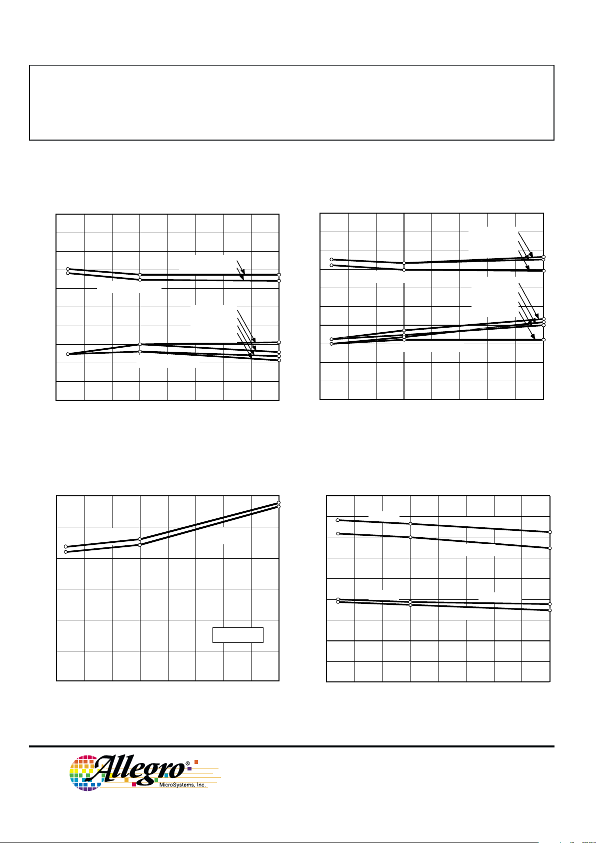
TYPICAL OPERATING CHARACTERISTICS
as a function of temperature
TOTAL SUPPLY CURRENT
OUTPUT SATURATION VOLTAGE
CHANNEL 2 SWITCH POINTS
0 50 100
AMBIENT TEMPERATURE IN °C
-50
Dwg. GH-026-7
SWITCH POINT IN GAUSS
0
5
150-25 25 75 125
10
15
20
25
-25
-20
-15
-10
-5
RELEASE POINT
VCC = 18-26.5 V
V
CC
= 3.3-5 V
VCC = 5 V
V
CC
= 3.3 V
V
CC
= 18 V
V
CC
= 26.5 V
OPERATE POINT
0 50 100
AMBIENT TEMPERATURE IN °C
-50
Dwg. GH-026-8
SWITCH POINT IN GAUSS
0
5
OPERATE POINT
150-25 25 75 125
10
15
20
25
-25
-20
-15
-10
-5
RELEASE POINT
VCC = 26.5 V
V
CC = 18 V
V
CC = 3.3-5 V
VCC = 26.5 V
V
CC = 5 V
V
CC = 18 V
V
CC = 3.3 V
CHANNEL 1 SWITCH POINTS
0 25 50 75 100
300
0
AMBIENT TEMPERATURE IN °C
200
100
-50
Dwg. GH-029-5
SATURATION VOLTAGE IN mV
150-25 125
I
OUT
= 20 mA
VCC = 26.5 V
VCC = 3.3 V
0
SUPPLY CURRENT IN mA
8
6
4
2
0 255075100
AMBIENT TEMPERATURE IN °C
-50
Dwg. GH-028-8
125-25 150
B ≥ B
OP
VCC = 18 V
VCC = 18 V
VCC = 3.3 V
VCC = 3.3 V
B ≤ B
RP
 Loading...