

查询3213供应商
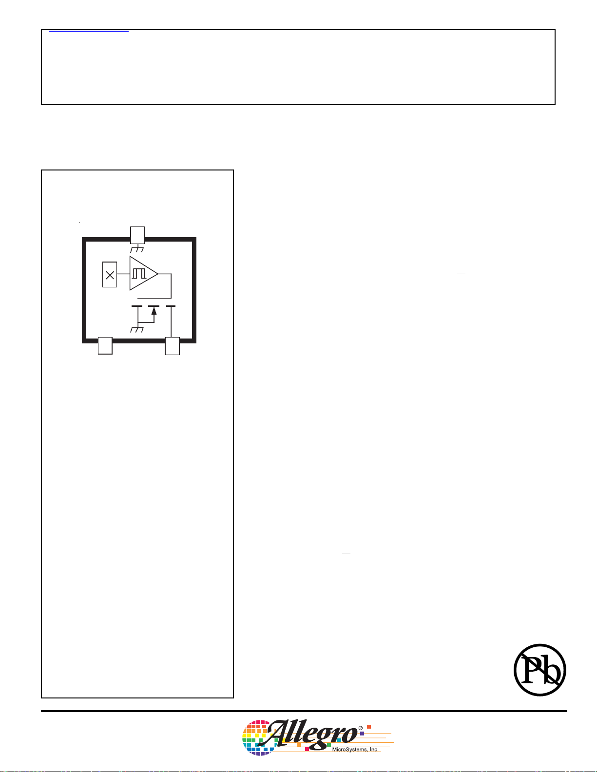
Package Designator ‘LH’ Pinning
(SOT23W)
3
V
DD
12
SUPPLY
Pinning is shown viewed from branded side.
ABSOLUTE MAXIMUM RATINGS
at TA = +25°C
Supply Voltage, VDD .............................. 6 V
Magnetic Flux Density, B .......... Unlimited
Output Off Voltage, V
Output Current, I
Junction Temperature, TJ ................ +170°C
Operating Temperature Range, TA
Suffix 'E' ...................... -40°C to +85°C
Suffix 'L' ................... -40°C to +150°C
Storage Temperature Range,
TS .............................. -65°C to +170°C
Caution: These CMOS devices have input
static protection (Class 3) but are still susceptible to damage if exposed to extremely
high static electrical charges.
GROUND
OUT
........................... 1 mA
OUT
OUTPUT
Dwg. PH-016-1
...................... 6 V
3213
AND
3214
MICROPOWER, ULTRA-SENSITIVE
HALL-EF FECT SWITCHES
The A3213xx and A3214xx integrated circuits are ultra-sensitive, pole
in de pen dent Hall-effect switches with a latched digital output. They are
es pe cial ly suited for operation in battery-operated, hand-held equip ment such
as cellular and cordless tele phones, pagers, and palmtop com put ers. A 2.4 volt
to 5.5 volt operation and a unique clocking scheme reduce the average op er at ing power requirements – the A3213xx to 825 µW, the A3214xx to 14 µW
(typical at 2.75 V)! Except for operating duty cycle and average operating
current, the A3213xx and A3214xx are identical.
Unlike other Hall-effect switches, either a north or south pole of suf fi cient
strength will turn the output on; in the absence of a magnetic field, the output
is off. The polarity independence and minimal power requirement allows
these devices to easily replace reed switches for superior reliability and ease of
manufacturing, while eliminating the requirement for signal conditioning.
Improved stability is made possible through chopper stabilization (dy nam ic offset cancellation), which reduces the residual offset voltage normally
caused by device overmolding, temperature de pen den cies, and thermal stress.
These devices include on a single silicon chip a Hall-voltage generator,
small-signal amplifier, chopper sta bi li za tion, a latch, and a MOSFET output.
Advanced BiCMOS processing is used to take advantage of low-voltage and
low-power requirements, component matching, very low input-offset errors,
and small component geometries.
Range 'E' devices are rated for operation over a tem per a ture range of
-40°C to +85°C; range 'L' devices are rated for operation over a tem per a ture
range of -40°C to +150°C. Two package styles provide a mag net i cal ly op ti mized pack age for most ap pli ca tions. ‘LH’ is a min ia ture low-profile surfacemount package, ‘UA’ is a three-lead SIP for through-hole mounting. Each
package is available in a lead (Pb) free version (suffix, –T) , with a 100% matte
tin plated leadframe.
FEATURES
■ Micropower Operation
■ Operate With North or South Pole
■ 2.4 V to 5.5 V Battery Operation
■ Chopper Stabilized
Superior Temperature Stability
Extremely Low Switch-Point Drift
Insensitive to Physical Stress
■ ESD Protected to 5 kV
■ Sol id-State Reliability
■ Small Size
■ Easily Manufacturable With Magnet Pole Independence
Data Sheet
27622.62F
3213
AND
3214
MICROPOWER,
ULTRA-SENSITIVE
HALL-EFFECT SWITCHES
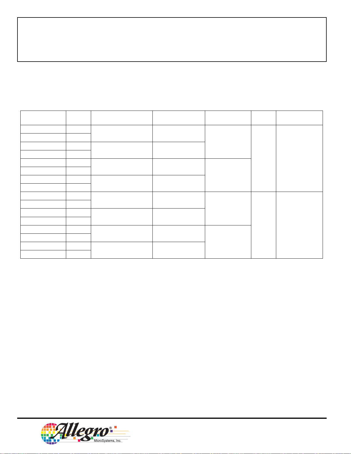
Product Selection Guide
Part Number Pb-free Packing* Mounting
A3213ELHLT –
A3213ELHLT-T Yes
A3213EUA –
A3213EUA-T Yes
A3213LLHLT –
A3213LLHLT-T Yes
A3213LUA –
A3213LUA-T Yes
A3214ELHLT –
A3214ELHLT-T Yes
A3214EUA –
A3214EUA-T Yes
A3214LLHLT –
A3214LLHLT-T Yes
A3214LUA –
A3214LUA-T Yes
*Contact Allegro for additional packing options.
7-in. reel
3000 pieces/reel
Bulk
500 pieces/bag
7-in. reel
3000 pieces/reel
Bulk
500 pieces/bag
7-in. reel
3000 pieces/reel
Bulk
500 pieces/bag
7-in. reel
3000 pieces/reel
Bulk
500 pieces/bag
Surface Mount
SIP through hole
Surface Mount
SIP through hole
Surface Mount
SIP through hole
Surface Mount
SIP through hole
Ambient, T
(ºC)
–40 to 85
–40 to 150
–40 to 85
–40 to 150
A
DC
(%)
25 460
0.10 11
I
DDAVG(TYP)
(µA)
2
115 Northeast Cutoff, Box 15036
Worcester, Massachusetts 01615-0036 (508) 853-5000
3213
AND
3214
MICROPOWER,
ULTRA-SENSITIVE
HALL-EFFECT SWITCHES
FUNCTIONAL BLOCK DIAGRAM
SUPPLY
SWITCH
X
TIMING
LOGIC
OUTPUT
& HOLD
DYNAMIC
SAMPLE
OFFSET CANCELLATION
800
700
600
500
400
300
200
100
ALLOWABLE PACKAGE POWER DISSIPATION in MILLIWATTS
0
PACKAGE
SUFFIX "LH"
R
θJA
= 228°C/W
20 60 100 140
40 80 120 180
PACKAGE
SUFFIX "UA"
R
θJA
= 165°C/W
TEMP.
CODE "E"
AMBIENT TEMPERATURE in °°°°C
TEMP.
CODE "L"
160
Dwg. GH-046-9
NOTE – Allowable package power dissipation will not be exceeded
unless Absolute Maximum Ratings (page 1) are exceeded.
LATCH
GROUND
Dwg. FH-020-5
Package Designator ‘UA’ Pinning
(SIP)
X
V
DD
1
SUPPLY
32
GROUND
Dwg. PH-016
OUTPUT
Pinning is shown viewed from branded side.
3
115 Northeast Cutoff, Box 15036
Worcester, Massachusetts 01615-0036 (508) 853-5000
Copyright © 2003 Allegro MicroSystems, Inc.
3213
AND
3214
MICROPOWER,
ULTRA-SENSITIVE
HALL-EFFECT SWITCHES
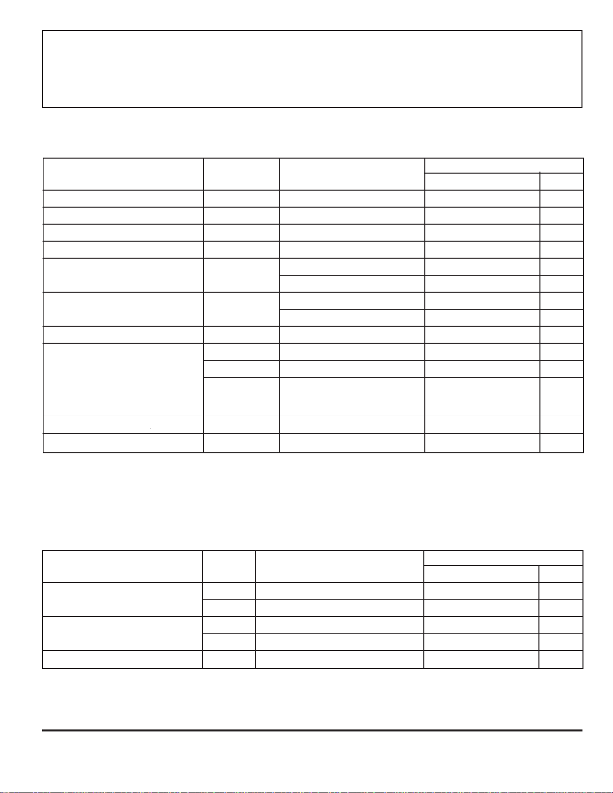
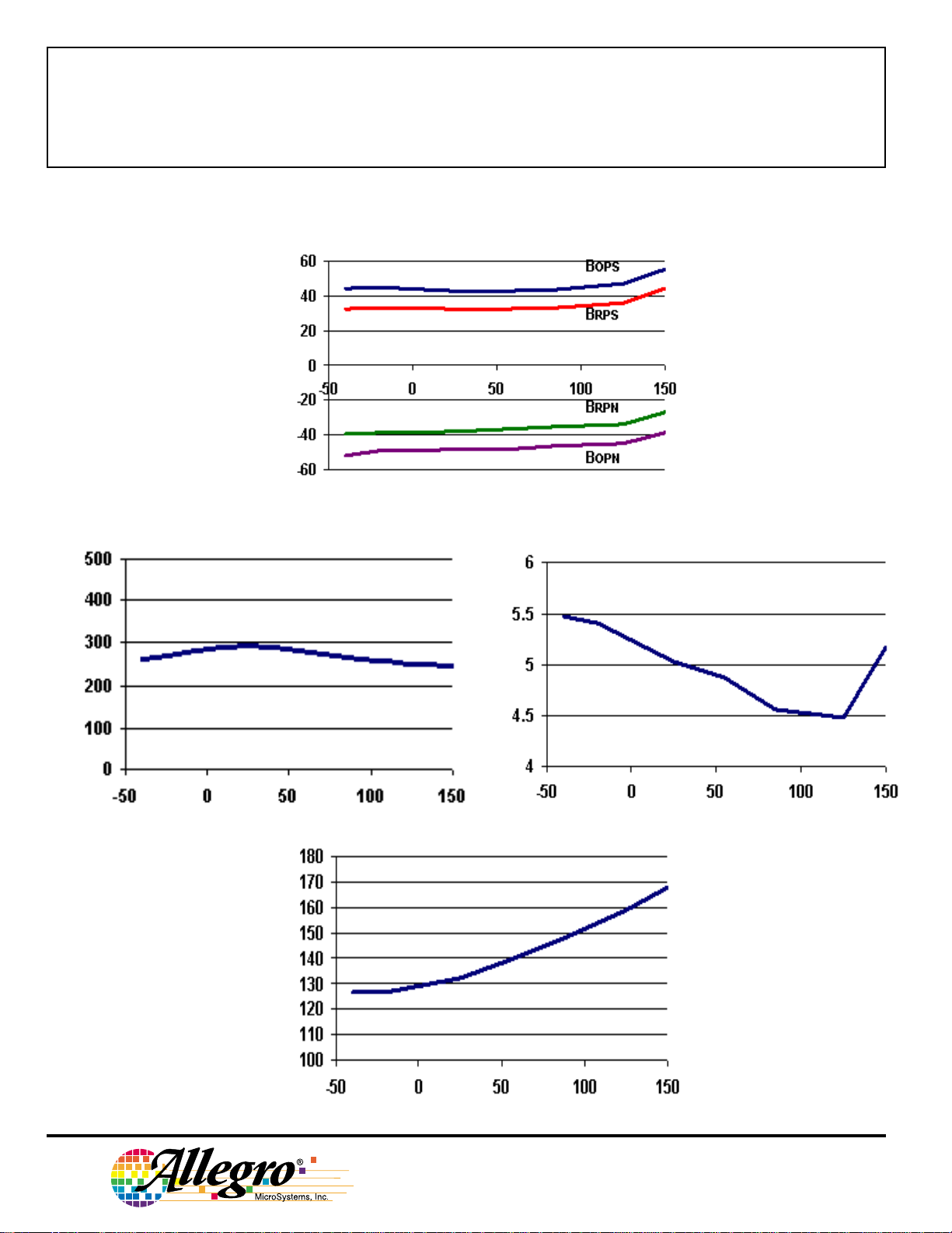
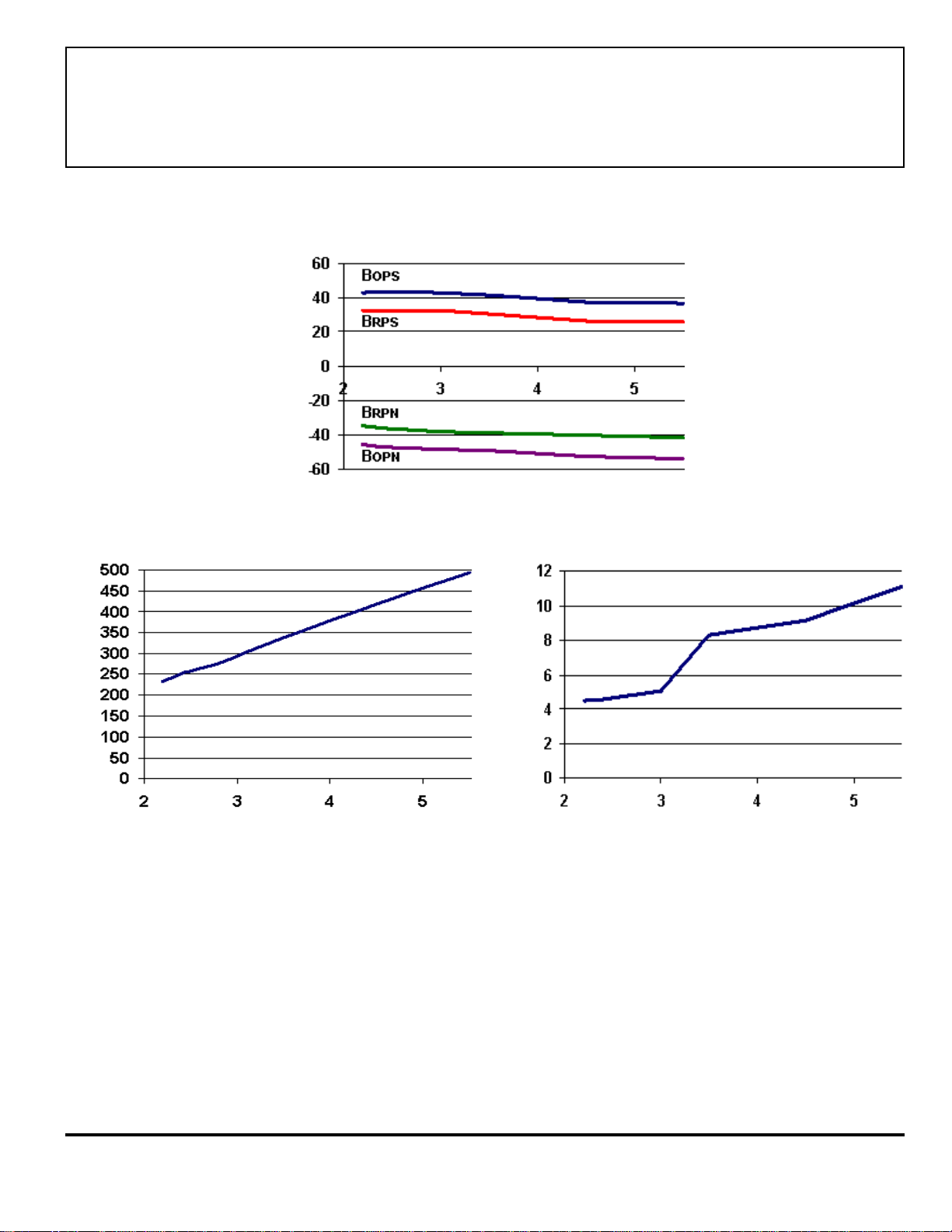
ELECTRICAL CHARACTERISTICS: unless otherwise noted
over operating voltage and temperature range.
Limits
Characteristic Symbol Test Conditions Min. Typ. Max. Units
Supply Voltage Range V
Output Leakage Current I
Output On Voltage V
Awake Time t
Period t
DD
OFF
OUT
awake
period
Operating
V
OUT
I
OUT
A3213xx – 240 360 µs
A3214xx – 60 90 ms
Duty Cycle d.c. A3213xx – 25 – %
A3214xx – 0.10 – %
Chopping Frequency f
Supply Current I
C
DD(EN)
I
DD(DIS)
I
DD(AVG)
Chip awake (enabled) – – 2.0 mA
Chip asleep (disabled) – – 8.0 µA
A3213xx – 460 850 µA
A3214xx – 11 22 µA
1)
= 5.5 V, B
RPN
< B < B
RPS
2.4 3.0 5.5 V
– <1.0 1.0 µA
= 1 mA, VDD = 3.0 V – 100 300 mV
–6090µs
– 340 – kHz
ESD, Human Body Model – Per CDF-AEC-Q100-002 5.0 – – kV
ESD, Machine Model – Per JESD22-A115 350 – – V
NOTES: 1. Operate and release points will vary with supply voltage.
= operate point (output turns ON); B
2. B
OPx
= release point (output turns OFF).
RPx
3. Typical Data is at TA = +25°C and VDD = 3.0 V and is for design information only.
MAGNETIC CHARACTERISTICS: over operating voltage and temperature range.
Limits
Characteristic Symbol Test Conditions Min. Typ. Max. Units
Operate Points B
Release Points B
Hysteresis B
OPS
B
OPN
RPS
B
RPN
hys
NOTES: 1. As used here, negative flux densities are defined as less than zero (algebraic convention) and -50 G is less than +10 G.
2. B
= operate point (output turns ON); B
OPx
3. Typical Data is at TA = +25°C and VDD = 3.0 V and is for design information only.
4. 1 gauss (G) is exactly equal to 0.1 millitesla (mT).
South pole to branded side – 42 70 G
North pole to branded side -70 -48 – G
South pole to branded side 10 32 – G
North pole to branded side – -38 -10 G
|B
- B
OPx
= release point (output turns OFF).
RPx
|–10–G
RPx
www.allegromicro.com
4
3213
AND
3214
MICROPOWER,
ULTRA-SENSITIVE
HALL-EFFECT SWITCHES
TYPICAL OPERATING CHARACTERISTICS
as a function of temperature (VDD = 3 V)
SWITCH POINTS, B (G)
A3213xx A3214xx
A)
µ
(
DD
I
AVG, SUPPLY CURRENT,
TEMPERATURE, T
(°C)
A
TEMPERATURE, T
A)
µ
(
DD
I
AVG, SUPPLY CURRENT,
(°C)
A
TEMPERATURE, T
(°C)
A
(mV)
OUT
V
OUTPUT ON VOLTAGE,
TEMPERATURE, T
5
115 Northeast Cutoff, Box 15036
Worcester, Massachusetts 01615-0036 (508) 853-5000
(°C)
A
HALL-EFFECT SWITCHES
TYPICAL OPERATING CHARACTERISTICS
as a function of supply voltage (T
SWITCH POINTS, B (G)
SUPPLY VOLTAGE, VDD (V)
= 25°C)
A
3213
AND
3214
MICROPOWER,
ULTRA-SENSITIVE
A3213xx A3214xx
A)
µ
(
DD
I
AVG, SUPPLY CURRENT,
SUPPLY VOLTAGE, VDD (V)
A)
µ
(
DD
I
AVG, SUPPLY CURRENT,
SUPPLY VOLTAGE, VDD (V)
www.allegromicro.com
6
3213
AND
3214
MICROPOWER,
ULTRA-SENSITIVE
HALL-EFFECT SWITCHES
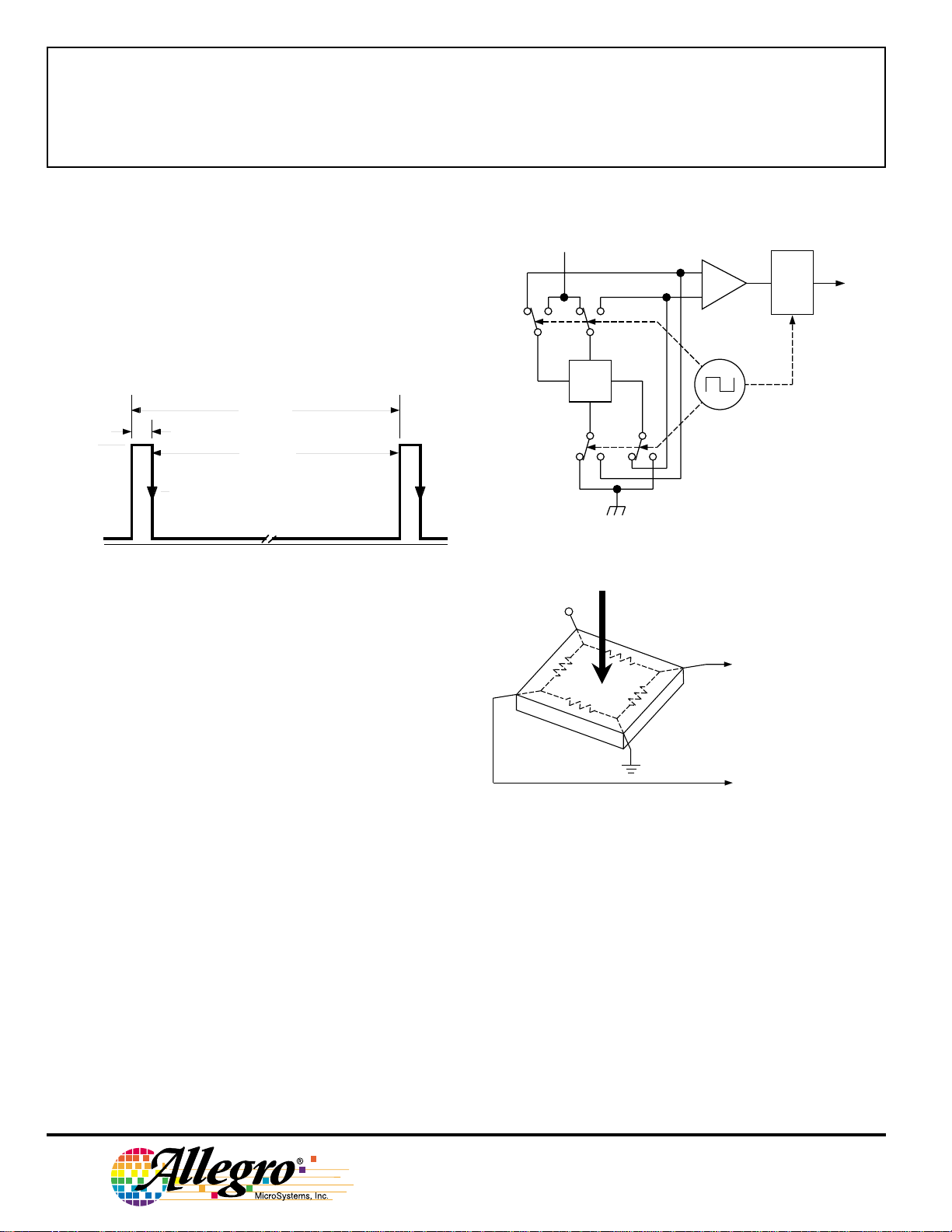
FUNCTIONAL DESCRIPTION
Low Average Power. Internal timing circuitry activates the
sensor for 60 µs and deactivates it for the remainder of the
period (240 µs for the A3213xx and 60 ms for the A3214xx).
A short "awake" time allows for stabilization prior to the
sensor sampling and data latching on the falling edge of the
timing pulse. The output during the "sleep" time is latched in
the last sampled state. The supply current is not affected by
the output state.
PERIOD
I
DD(EN)
I
DD(DIS)
0
60 µs - "AWAKE"
"SLEEP"
SAMPLE &
OUTPUT LATCHED
Dwg. WH-017-1
Chopper-Stabilized Technique. The Hall element can be
considered as a resistor array similar to a Wheatstone bridge.
A large portion of the offset is a result of the mismatching of
these resistors. These devices use a proprietary dynamic offset
cancellation technique, with an internal high-frequency clock
to reduce the residual offset voltage of the Hall element that is
normally caused by device overmolding, temperature dependencies, and thermal stress. The chopper-stabilizing technique
cancels the mismatching of the resistor circuit by changing the
direction of the current flowing through the Hall plate using
CMOS switches and Hall voltage measurement taps, while
maintaing the Hall-voltage signal that is induced by the
external magnetic flux. The signal is then captured by a
sample-and-hold circuit and further processed using low-offset
bipolar circuitry. This technique produces devices that have an
extremely stable quiescent Hall output voltage, are immune to
thermal stress, and have precise recoverability after temperature cycling. This technique will also slightly degrade the
device output repeatability. A relatively high sampling
frequency is used in order that faster signals can be processed.
More detailed descriptions of the circuit operation can be
found in Technical Paper STP 97-10, Monolithic Magnetic
Hall Sensor Using Dynamic Quadrature Offset Cancellation
and Technical Paper STP 99-1, Chopper-Stabilized Amplifiers
With A Track-and-Hold Signal Demodulator.
+V
& HOLD
SAMPLE
X
Dwg. EH-012-1
B
+V
—
HALL
VOLTAGE
+
Dwg. AH-011-2
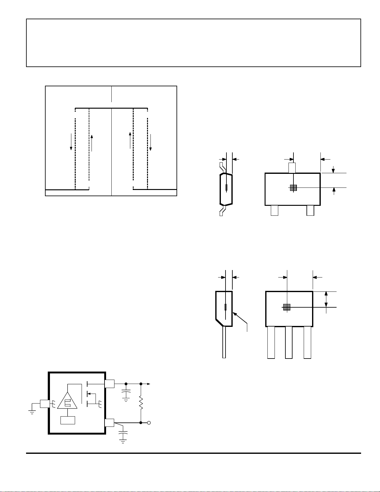
Operation. The output of this device switches low (turns on)
when a magnetic field perpendicular to the Hall sensor exceeds
the operate point B
(or is less than B
OPS
). After turn-on,
OPN
the output is capable of sinking up to 1 mA and the output
voltage is V
the release point B
. When the magnetic field is reduced below
OUT(ON)
(or increased above B
RPS
RPN
), the device
output switches high (turns off). The difference in the magnetic operate and release points is the hysteresis (B
) of the
hys
device. This built-in hysteresis allows clean switching of the
output even in the presence of external mechanical vibration
and electrical noise.
As used here, negative flux densities are defined as less
than zero (algebraic convention) and -50 G is less than +10 G.
7
115 Northeast Cutoff, Box 15036
Worcester, Massachusetts 01615-0036 (508) 853-5000
5 V
MAX
B
OPN
Allegro
OUTPUT OFF
B
OPS
3213
AND
3214
MICROPOWER,
ULTRA-SENSITIVE
HALL-EFFECT SWITCHES
SENSOR LOCATIONS
Package Designator ‘LH’
OUTPUT VOLTAGE
B
RPN
0
-B
0
MAGNETIC FLUX
B
RPS
OUTPUT ON
+B
Dwg. GH-043-1
Applications. Allegro's pole-independent sensing technique
allows for operation with either a north pole or south pole
magnet orientation, enhancing the manufacturability of the
device. The state-of-the-art technology provides the same
output polarity for either pole face.
It is strongly recommended that an external bypass
capacitor be connected (in close proximity to the Hall sensor)
between the supply and ground of the device to reduce both
external noise and noise generated by the chopper-stabilization
technique. This is especially true due to the relatively high
impedance of battery supplies.
The simplest form of magnet that will operate these
devices is a bar magnet with either pole near the branded
surface of the device. Many other methods of operation are
possible. Extensive applications information on magnets and
Hall-effect sensors is also available in the Allegro Electronic
Data Book AMS-702 or Application Note 27701, or at
ACTIVE AREA DEPTH
0.011"
0.28 mm
NOM
Package Designator ‘UA’
ACTIVE AREA DEPTH
0.0195"
0.50 mm
NOM
BRANDED
SURFACE
3
A
1 2
2.07 mm
A
1
2
0.059"
1.51 mm
0.046"
0.85 mm
Dwg. MH-025-1
0.081"
0.053"
1.33 mm
3
www.allegromicro.com
3
X
www.allegromicro.com
Dwg. MH-011-12
2
10 pF
1
DD
V
0.1 µF
OUTPUT
50 kΩ
SUPPLY
(3 V BATTERY)
Dwg. EH-013-2
8

3213
7
AND
3214
MICROPOWER,
ULTRA-SENSITIVE
HALL-EFFECT SWITCHES
PACKAGE DESIGNATOR ‘LH’
(SOT23W, fits SC-59A solder-pad layout)
0.083
0.073
0.022
REF
0.006
0.000
0.122
0.114
0.020
0.012
12
Dimensions in Inches
(for reference only)
3
0.118
0.106
GAUGE PLANE
SEATING PLANE
0.037
BSC
0.045
0.0079
0.0050
0.032
0° TO 8°
0.010
BSC
Dwg. MA-010-3D in
0.010
MIN
0.55
REF
0.15
0.00
2.10
1.85
Dimensions in Millimeters
3.10
2.90
0.50
0.30
3
12
(controlling dimensions)
3.00
2.70
GAUGE PLANE
SEATING PLANE
0° TO 8°
0.95
BSC
1.13
0.20
0.127
0.87
0.25
BSC
0.25
MIN
Dwg. MA-010-3D mm
0.039
0.028
3
1.00
0.70
3
0.094
12
12
0.03
Dwg. MA-011-3 in
Dwg. MA-011-3 mm
NOTES: 1. Tolerances on package height and width represent allowable mold offsets. Dimensions given are
measured at the widest point (parting line).
2. Exact body and lead configuration at vendor’s option within limits shown.
3. Height does not include mold gate flash.
4. Where no tolerance is specified, dimension is nominal.
5. Add "LT" to part number for tape and reel.
9
115 Northeast Cutoff, Box 15036
Worcester, Massachusetts 01615-0036 (508) 853-5000
2.40
0.95

Dimensions in Inches
Dwg. MH-014E mm
4.17
4.04
1.57
1.47
0.44
0.35
1.27
BSC
45°
16.26
15.24
0.48
0.36
2.16
MAX
45°
0.79
123
3.10
2.97
SEE NOTE
(controlling dimensions)
0.164
0.159
HALL-EFFECT SWITCHES
PACKAGE DESIGNATOR ‘UA’
Dimensions in Millimeters
3213
AND
MICROPOWER,
ULTRA-SENSITIVE
(for reference only)
3214
0.062
0.058
45°
0.031
0.0173
0.0138
0.0189
0.0142
Dwg. MH-014E in
SEE NOTE
45°
0.122
0.117
0.640
0.600
0.085
123
MAX
0.050
BSC
NOTES: 1. Tolerances on package height and width represent
allowable mold offsets. Dimensions given are
measured at the widest point (parting line).
2. Exact body and lead configuration at vendor’s option
within limits shown.
3. Height does not include mold gate flash.
4. Recommended minimum PWB hole diameter to clear
transition area is 0.035" (0.89 mm).
5. Where no tolerance is specified, dimension is nominal.
6. Supplied in bulk pack (500 pieces per bag).
Radial Lead Form (order A321xxUA-LC)
123
0.620"
0.500"
(15.7 mm
12.7 mm)
0.108"
(2.74 mm)
www.allegromicro.com
0.100"
(2.5 mm)
Dwg. MH-026
NOTE: Lead-form dimensions are the nominals produced on the
forming equipment. No dimensional tolerance is implied
or guaranteed for bulk packaging (500 pieces per bag).
10

3213
AND
3214
MICROPOWER,
ULTRA-SENSITIVE
HALL-EFFECT SWITCHES
11
The products described herein are manufactured under one or more
of the following U.S. patents: 4,761,569; 5,619,137; 5,621,319. In
addition, a patent is pending for Allegro's magnetic pole-independent
feature. Allegro has several foreign counterpart patents as well.
Allegro has not licensed any of these patents to any third party.
Allegro MicroSystems, Inc. reserves the right to make, from time to
time, such departures from the detail specifications as may be required
to permit improvements in the performance, reliability, or
manufacturability of its products. Before placing an order, the user is
cautioned to verify that the information being relied upon is current.
Allegro products are not authorized for use as critical components
in life-support appliances, devices, or systems without express written
approval.
The information included herein is believed to be accurate and
reliable. However, Allegro MicroSystems, Inc. assumes no responsibility for its use; nor for any infringements of patents or other rights of
third parties that may result from its use.
115 Northeast Cutoff, Box 15036
Worcester, Massachusetts 01615-0036 (508) 853-5000
 Loading...