

Page 1

查询A3240ELTTR供应商
3240
CHOPPER-STABILIZED, PRECISION
HALL-EF FECT SWITCH
Data Sheet
27621.20c
Suffi x ‘–LT’ & ‘–UA’ Pinning
(SOT89/TO-243AA & ultra-min SIP)
X
PTCT
V
CC
1
SUPPLY
Pinning is shown viewed from branded side.
32
GROUND
Dwg. PH-003-2
OUTPUT
The A3240-- Hall-effect switch is an extremely temperature-stable
and stress-resistant sensor especially suited for operation over extended
tem per a ture ranges to +150°C. Superior high-temperature per for mance
is made possible through dynamic offset cancellation, which reduces the
residual offset voltage normally caused by device overmolding, tem per a ture de pen den cies, and thermal stress.
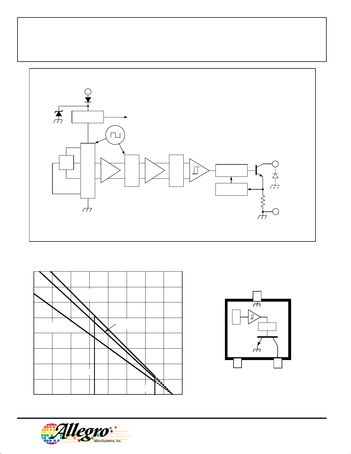
The device includes on a single silicon chip a voltage regulator, Hallvoltage generator, small-signal amplifi er, chopper sta bi li za tion, Schmitt
trigger, and a short-circuit protected open-collector output to sink up to
25 mA. A south pole of suffi cient strength will turn the output on. An
on-board regulator permits operation with supply voltages of 4.2 to 24
volts.
Three package styles provide a magnetically op ti mized pack age for
most ap pli ca tions. Package type LH is a modifi ed SOT23W surface-
mount package, LT is a miniature SOT89/TO-243AA transistor package
for surface-mount applications; while UA is a three-lead ultra-mini-SIP
for through-hole mounting. The LH and UA packages are also available
in a lead (Pb) free version (suffix, –T) , with a 100% matte tin plated
leadframe.
ABSOLUTE MAXIMUM RATINGS
at TA = +25°C
Supply Voltage, VCC .......................... 26.5 V
Reverse Battery Voltage, V
Magnetic Flux Density, B............ Unlimited
Output OFF Voltage, V
Continuous Output Current,
I
Reverse Output Current, I
Package Power Dissipation, PD See Graph
Junction Temperature, TJ ................ +170°C
Operating Temperature Range, T
Range ‘L’.................... -40°C to +150°C
Storage Temperature Range,
TS .............................. -65°C to +170°C
*Internal current limiting is intended to protect
the device from output short circuits.
......................................... 25 mA*
OUT
Range ‘E’ ..................... -40°C to +85°C
.......... -30 V
RCC
.................. 26 V
OUT
......... -50 mA
OUT
A
FEATURES
■ Resistant to Physical Stress
■ Superior Temperature Stability
■ Output Short-Circuit Protection
■ Operation From Unregulated Supply
■ Reverse Battery Protection
■ Sol id-State Reliability
■ Small Size
Page 2

Product Selection Guide
Part Number Pb-free Packing* Mounting
A3240ELHLT – 7-in. reel, 3000 pieces/reel Surface Mount
A3240ELHLT-T Yes 7-in. reel, 3000 pieces/reel Surface Mount
A3240ELT – Bulk, 500 pieces/bag Surface Mount
A3240ELTTR – 7-in. reel, 3000 pieces/reel Surface Mount
A3240EUA – Bulk, 500 pieces/bag SIP through hole
A3240EUA-T Yes Bulk, 500 pieces/bag SIP through hole
A3240LLHLT – 7-in. reel, 3000 pieces/reel Surface Mount
A3240LLHLT-T Yes 7-in. reel, 3000 pieces/reel Surface Mount
A3240LLT – Bulk, 500 pieces/bag Surface Mount
A3240LLTTR – 7-in. reel, 3000 pieces/reel Surface Mount
A3240LUA – Bulk, 500 pieces/bag SIP through hole
A3240LUA-T Yes Bulk, 500 pieces/bag SIP through hole
*Contact Allegro for additional packing options.
3240
CHOPPER-STABILIZED,
PRECISION
HALL-EFFECT SWITCH
Ambient, T
(ºC)
–40 to 85
–40 to 150
A
B
RP(MIN)
(G)
5.0 50
B
OP(MAX)
(G)
www.allegromicro.com
2
Page 3
3240
CHOPPER-STABILIZED,
PRECISION
HALL-EFFECT SWITCH
SUPPLY
FUNCTIONAL BLOCK DIAGRAM
800
700
600
X
REG.
DYNAMIC
OFFSET CANCELLATION
Suffix "–UA"
R
θJA
= 165°C/W
TO ALL
SUBCIRCUITS
& HOLD
SAMPLE
FILTER
LOW-PASS
OUTPUT
CONTROL
CURRENT
LIMIT
<1Ω
GROUND
Dwg. FH-020-1
Suffix ‘–LH’ Pinning
(SOT23W)
3
500
Suffix "–LH"
R
θJA
400
300
200
100
ALLOWABLE PACKAGE POWER DISSIPATION in MILLIWATTS
0
20 60 100 140
= 228°C/W
Suffix "E–"
40 80 120 180
AMBIENT TEMPERATURE in °°°°C
3
Suffix "–LT"
R
θJA
= 180°C/W
V
Suffix "L–"
160
Dwg. GH-046-2D
115 Northeast Cutoff, Box 15036
Worcester, Massachusetts 01615-0036 (508) 853-5000
Copyright © 2000, 2003, 2004 Allegro MicroSystems, Inc.
X
PTCT
CC
12
SUPPLY
GROUND
Dwg. PH-003-4
OUTPUT
Page 4
3240
CHOPPER-STABILIZED,
PRECISION
HALL-EFFECT SWITCH
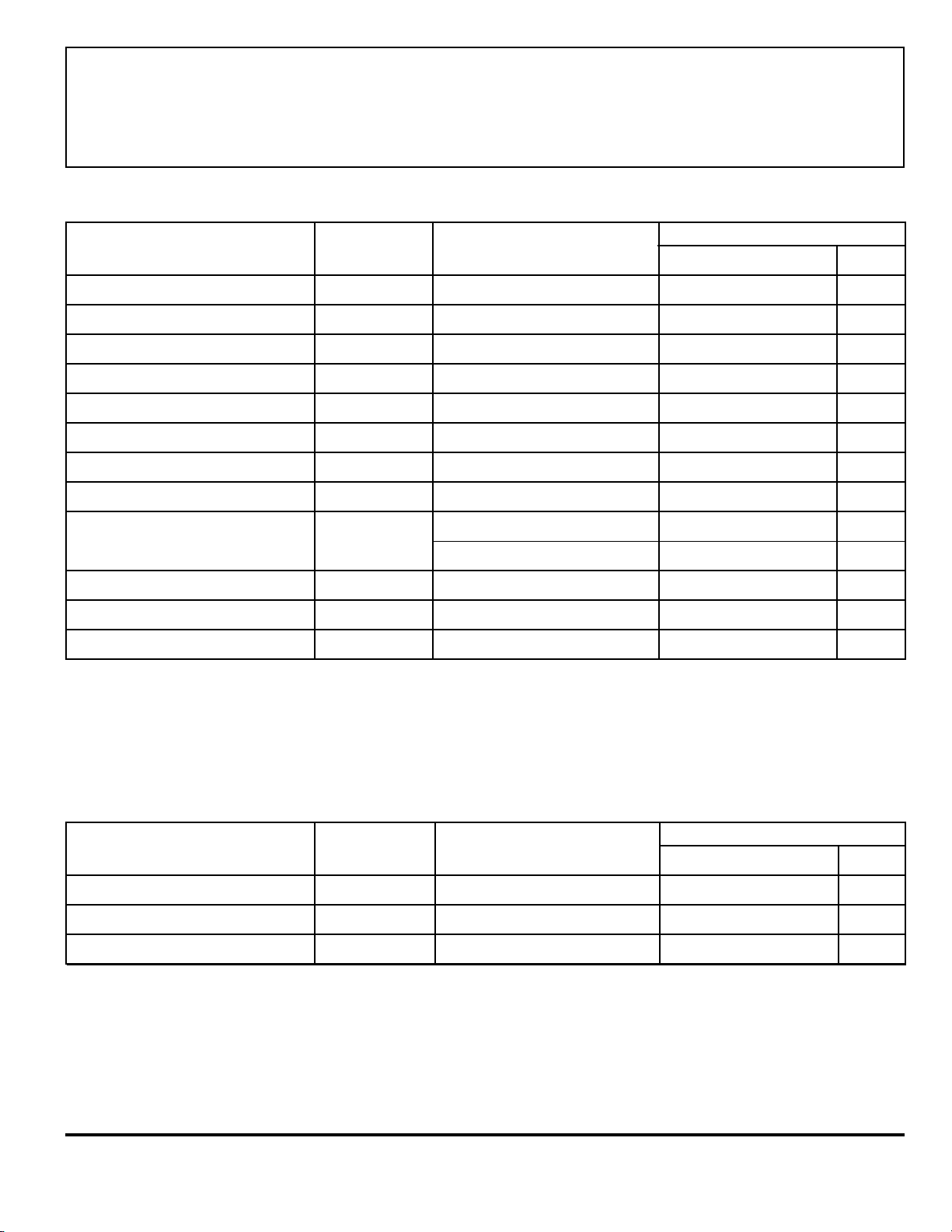
ELECTRICAL CHARACTERISTICS over operating temperature range.
Limits
Characteristic Symbol Test Conditions Min. Typ. Max. Units
Supply Voltage Range V
Output Leakage Current I
Output Saturation Voltage V
OUT(SAT)
Output Current Limit I
Power-On Time t
Chopping Frequency f
Output Rise Time t
Output Fall Time t
Supply Current I
CC
OFF
OM
po
C
r
f
CC
Operating, TJ < 165°C
V
= 24 V, B < B
OUT
I
= 20 mA, B > B
OUT
B > B
OP
VCC > 4.2 V – – 50 µs
RL = 820 Ω, CL = 20 pF – 0.2 2.0 µs
RL = 820 Ω, CL = 20 pF – 0.1 2.0 µs
B < BRP, VCC = 12 V – 3.0 6.0 mA
1
RP
OP
B > BOP, VCC = 12 V – 4.0 6.0 mA
Reverse Battery Current I
CC
Zener Voltage VZ + V
Zener Impedance zz + z
D
D
V
= -30 V – – -5.0 mA
RCC
ICC = 15 mA, TA = 25°C 283237 V
ICC = 15 mA, TA = 25°C–50–Ω
NOTES: 1. Maximum voltage must be adjusted for power dissipation and junction temperature.
2. BOP = operate point (output turns on); BRP = release point (output turns off).
3. Typical Data is at TA = +25°C and VCC = 12 V and is for design information only.
4.2–24V
––10µA
– 185 500 mV
30 – 60 mA
– 340 – kHz
MAGNETIC CHARACTERISTICS over operating supply voltage and temperature ranges.
Limits
Characteristic Symbol Test Conditions Min. Typ. Max. Units
Operate Point B
Release Point B
Hysteresis B
OP
RP
hys
BOP - B
RP
NOTES: 1. Typical Data is at TA = +25°C and VCC = 12 V and is for design information only.
2. 1 gauss (G) is exactly equal to 0.1 millitesla (mT).
www.allegromicro.com
–3550G
5.0 25 – G
–10– G
4
Page 5
3240
CHOPPER-STABILIZED,
PRECISION
HALL-EFFECT SWITCH
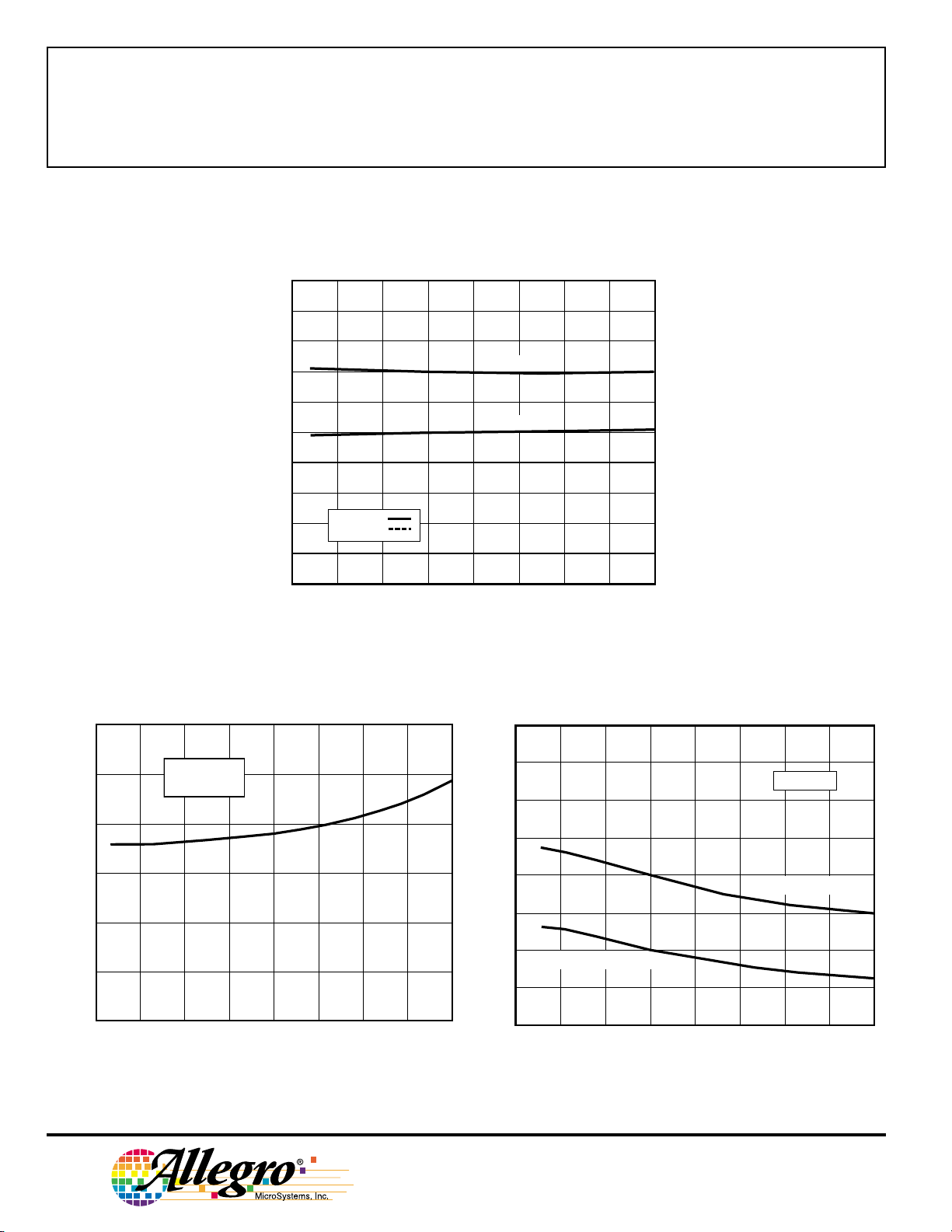
TYPICAL OPERATING CHARACTERISTICS
50
40
30
20
as a function of temperature
SWITCH POINTS
OPERATE POINT
RELEASE POINT
OUTPUT SATURATION VOLTAGE
300
IOUT = 20 mA
VCC = 12 V
200
100
SATURATION VOLTAGE IN mV
SWITCH POINTS IN GAUSS
10
0
-50
VCC = 4.5 V
CC
= 24 V
V
0 50 100
AMBIENT TEMPERATURE IN °°°°C
SUPPLY CURRENT
6.0
5.0
4.0
SUPPLY CURRENT IN mA
3.0
OUTPUT OFF, B < B
150-25 25 75 125
Dwg. GH-026-5
RP
VCC = 12 V
OUTPUT ON, B > B
OP
0
-50
0 25 50 75 100
AMBIENT TEMPERATURE IN °°°°C
150-25 125
Dwg. GH-029-4
2.0
-50
0 25 50 75 100
AMBIENT TEMPERATURE IN °°°°C
125-25 150
Dwg. GH-028-5
115 Northeast Cutoff, Box 15036
5
Worcester, Massachusetts 01615-0036 (508) 853-5000
Page 6
CHOPPER-STABILIZED,
HALL-EFFECT SWITCH
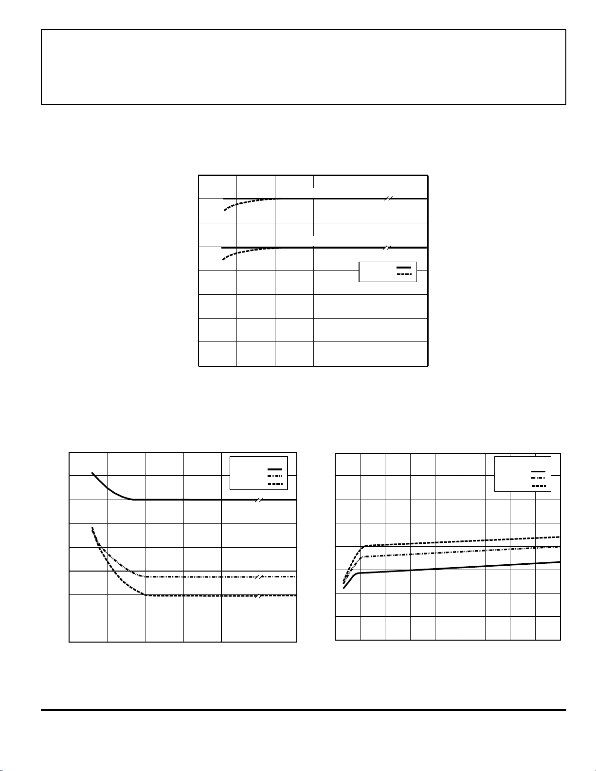
TYPICAL OPERATING CHARACTERISTICS
as a function of supply voltage
SWITCH POINTS
40
OPERATE POINT
30
RELEASE POINT
3240
PRECISION
250
225
200
20
10
SWITCH POINT IN GAUSS
0
3.0
3.5
OUTPUT SATURATION VOLTAGE
IOUT = 20 mA
TA = 150°C
A = +25°C
T
A = -40°C
T
4.0 4.5 5.0
SUPPLY VOLTAGE IN VOLTS
8.0
7.0
6.0
5.0
4.0
TA = 150°C
A
= -40°C
T
24
Dwg. GH-021-2
SUPPLY CURRENT
OUTPUT ON
TA = 150°C
A
= +25°C
T
A
= -40°C
T
175
SATURATION VOLTAGE IN mV
150
3.0
3.5
4.0 4.5 5.0
SUPPLY VOLTAGE IN VOLTS
www.allegromicro.com
24
Dwg. GH-055-1
3.0
SUPPLY CURRENT IN mA
2.0
1.0
0
4.0 6.0 9.0
3.0
5.0 12
SUPPLY VOLTAGE IN VOLTS
10 118.07.0
Dwg. GH-058-4
6
Page 7
3240
CHOPPER-STABILIZED,
PRECISION
HALL-EFFECT SWITCH
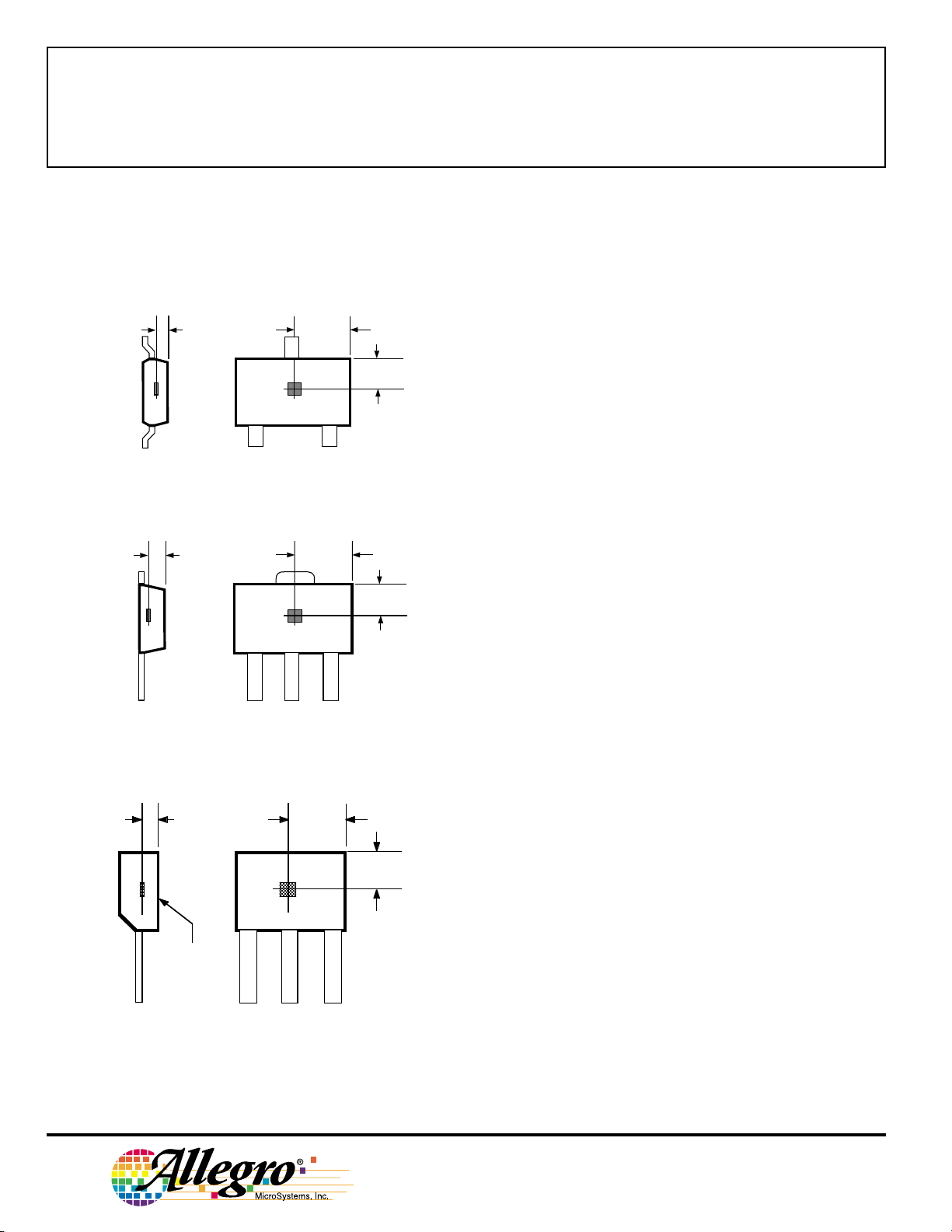
SENSOR LOCATIONS
Package Designator ‘LH’
ACTIVE AREA DEPTH
0.011"
0.28 mm
NOM
A
1
Package Designator ‘LT’
ACTIVE AREA DEPTH
0.0305"
0.775 mm
NOM
A
1 32
Package Designator ‘UA’
3
0.059"
1.49 mm
2
0.088"
2.24 mm
0.038"
0.96 mm
Dwg. MH-025
0.045"
1.14 mm
Dwg. MH-008-8A
ACTIVE AREA DEPTH
0.0195"
0.50 mm
NOM
0.080"
2.04 mm
0.056"
1.44 mm
The products described herein are manufactured under one or
more of the following U.S. patents: 5,045,920; 5,264,783; 5,442,283;
5,389,889; 5,581,179; 5,517,112; 5,619,137; 5,621,319; 5,650,719;
Allegro
5,686,894; 5,694,038; 5,729,130; 5,917,320; and other patents
pending.
Allegro MicroSystems, Inc. reserves the right to make, from time to
time, such departures from the detail specifications as may be
required to permit improvements in the performance, reliability, or
manufacturability of its products. Before placing an order, the user is
cautioned to verify that the information being relied upon is current.
BRANDED
SURFACE
A
2
1
3
Allegro products are not authorized for use as critical components
in life-support appliances, devices, or systems without express written
Dwg. MH-011-9B
approval.
The information included herein is believed to be accurate and
reliable. However, Allegro MicroSystems, Inc. assumes no responsibility for its use; nor for any infringements of patents or other rights of
third parties that may result from its use.
7
115 Northeast Cutoff, Box 15036
Worcester, Massachusetts 01615-0036 (508) 853-5000
Page 8
FUNCTIONAL DESCRIPTION
3240
CHOPPER-STABILIZED,
PRECISION
HALL-EFFECT SWITCH
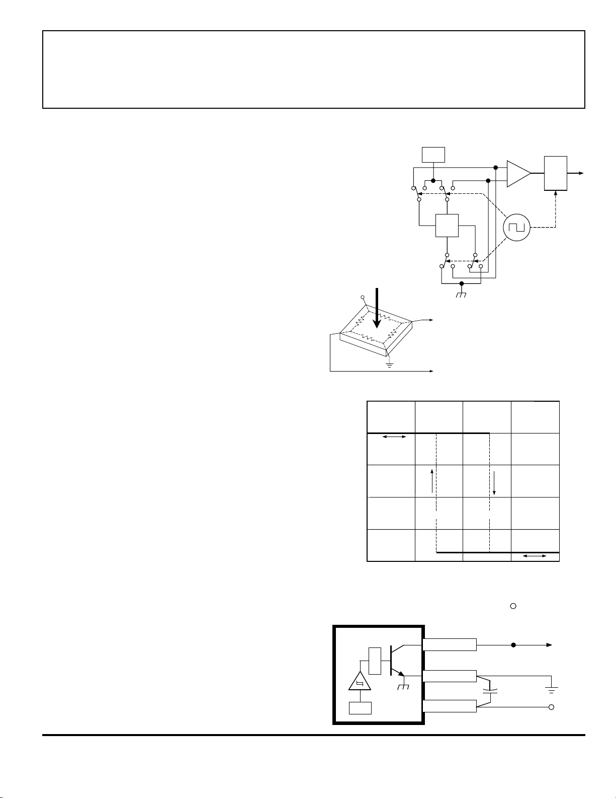
Chopper-Stabilized Technique. The Hall element can be
considered as a resistor array similar to a Wheatstone bridge. A
large portion of the offset is a result of the mismatching of these
resistors. These devices use a proprietary dynamic offset
cancellation technique, with an internal high-frequency clock to
reduce the residual offset voltage of the Hall element that is
normally caused by device overmolding, temperature dependencies, and thermal stress. The chopper-stabilizing technique
cancels the mismatching of the resistor circuit by changing the
direction of the current flowing through the Hall plate using
CMOS switches and Hall voltage measurement taps, while
maintaing the Hall-voltage signal that is induced by the external
magnetic flux. The signal is then captured by a sample-andhold circuit and further processed using low-offset bipolar
circuitry. This technique produces devices that have an
extremely stable quiescent Hall output voltage, are immune to
thermal stress, and have precise recoverability after temperature
cycling. This technique will also slightly degrade the device
output repeatability. A relatively high sampling frequency is
used in order that faster signals can be processed.
More detailed descriptions of the circuit operation can be
found in: Technical Paper STP 97-10, Monolithic Magnetic
Hall Sensor Using Dynamic Quadrature Offset Cancellation
and Technical Paper STP 99-1, Chopper-Stabilized Amplifiers
With A Track-and-Hold Signal Demodulator.
Operation. The output of these devices switches low (turns
on) when a magnetic field (south pole) perpendicular to the Hall
sensor exceeds the operate point threshold (BOP). After turn-on,
the output is capable of sinking 25 mA and the output voltage is
V
OUT(SAT)
. When the magnetic field is reduced below the
release point (BRP), the device output goes high (turns off). The
difference in the magnetic operate and release points is the
hysteresis (B
) of the device. This built-in hysteresis allows
hys
clean switching of the output even in the presence of external
mechanical vibration and electrical noise.
Applications. It is strongly recommended that an external
bypass capacitor be connected (in close proximity to the Hall
sensor) between the supply and ground of the device to reduce
both external noise and noise generated by the chopperstabilization technique.
The simplest form of magnet that will operate these devices
is a ring magnet. Other methods of operation, such as linear
magnets, are possible. Extensive applications information on
magnets and Hall-effect sensors is also available in Application
Note 27701, or at
www.allegromicro.com
B
+V
+V
V
CC
OUTPUT VOLTAGE
0
0
PTCT
X
Dwg. AH-011-2
CC
V
REG
HALL
VOLTAGE
X
—
+
B
RP
FLUX DENSITY
3
2
1
& HOLD
SAMPLE
Dwg. EH-012
B
OP
V
OUT(SAT)
+B
Dwg. GH-007-2
SUPPLY
OUTPUT
0.1 µF
SUPPLY
Dwg. EH-013
www.allegromicro.com
8
Page 9
3240
7
CHOPPER-STABILIZED,
PRECISION
HALL-EFFECT SWITCH
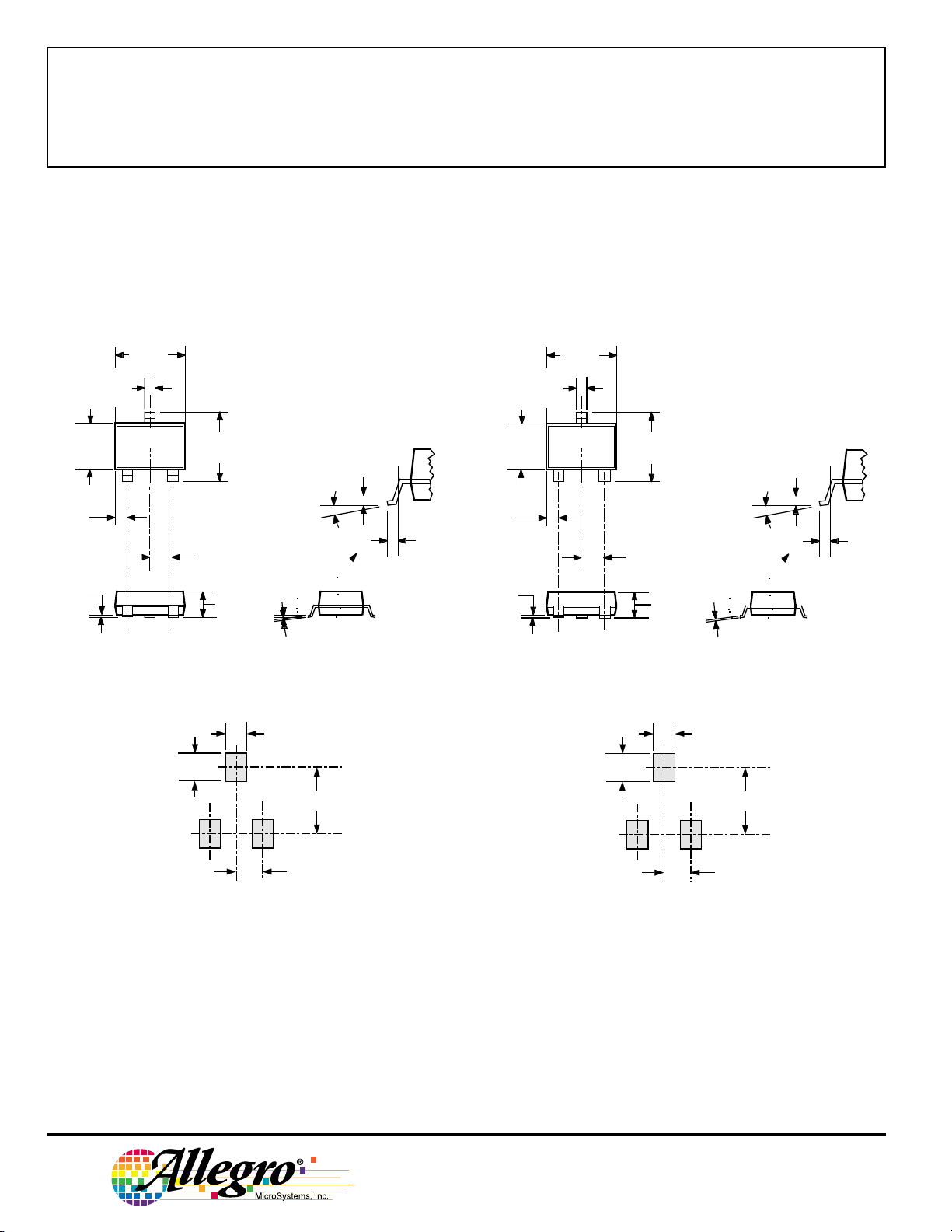
PACKAGE DESIGNATOR ‘LH’
(fits SC-59A solder-pad layout)
0.083
0.073
0.022
REF
0.006
0.000
0.122
0.114
0.020
0.012
12
Dimensions in Inches
(for reference only)
3
0.118
0.106
GAUGE PLANE
SEATING PLANE
0.037
BSC
0.045
0.0079
0.0050
0.032
0° TO 8°
0.010
BSC
Dwg. MA-010-3D in
0.010
MIN
0.55
REF
0.15
0.00
2.10
1.85
Dimensions in Millimeters
3.10
2.90
0.50
0.30
3
12
(controlling dimensions)
3.00
2.70
GAUGE PLANE
SEATING PLANE
0.95
BSC
1.13
0° TO 8°
0.20
0.127
0.87
0.25
BSC
Dwg. MA-010-3D mm
0.25
MIN
0.028
3
0.039
0.094
12
0.03
Dwg. MA-011-3 in
1.00
12
NOTES: 1. Tolerances on package height and width represent allowable mold offsets. Dimensions given are
measured at the widest point (parting line).
2. Exact body and lead configuration at vendor’s option within limits shown.
3. Height does not include mold gate flash.
4. Where no tolerance is specified, dimension is nominal.
5. Add "LT" to part number for tape and reel.
9
115 Northeast Cutoff, Box 15036
Worcester, Massachusetts 01615-0036 (508) 853-5000
0.70
3
2.40
0.95
Dwg. MA-011-3 mm
Page 10
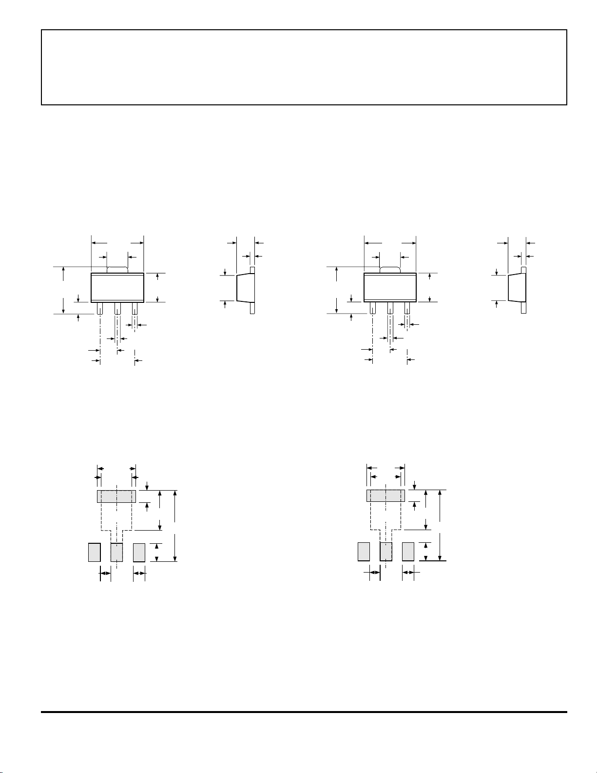
PACKAGE DESIGNATOR ‘LT’
(SOT89/TO-243AA)
3240
CHOPPER-STABILIZED,
PRECISION
HALL-EFFECT SWITCH
0.167
0.155
0.047
0.035
0.059
BSC
Dimensions in Inches
(for reference only)
0.181
0.173
0.072
0.064
0.102
0.0221
0.0173
0.090
0.0189
0.0142
1
23
0.118
BSC
0.063
0.055
0.090
0.084
0.0173
0.0138
Dwg. MA-009-3A in
4.25
3.94
1.20
0.89
1.50
BSC
Dimensions in Millimeters
(controlling dimensions)
4.60
4.40
1.83
1.62
2.60
0.56
0.44
2.29
0.48
0.36
1
23
3.00
BSC
1.60
1.40
2.29
2.13
0.44
0.35
Dwg. MA-009-3A mm
0.098
0.079
B
1
0.028
TYP
Pads 1, 2, 3, and A — Standard SOT89 Layout
Pads 1, 2, 3, and B — Low-Stress Version
Pads 1, 2, and 3 only — Lowest Stress, But Not Self Aligning
0.031
A
2
0.102
0.181
0.047
3
0.031
TYP
Dwg. MA-012-3 in
0.7
TYP
Pads 1, 2, 3, and A — Standard SOT89 Layout
Pads 1, 2, 3, and B — Low-Stress Version
Pads 1, 2, and 3 only — Lowest Stress, But Not Self Aligning
NOTES: 1. Exact body and lead configuration at vendor’s option within limits shown.
2. Supplied in bulk pack (500 pieces per bag) or add "TR" to part number for tape and reel.
3. Only low-temperature (≤240°C) reflow-soldering techniques are recommended for SOT89 devices.
www.allegromicro.com
2.5
2.0
B
13
0.8
A
2
2.6
1.2
0.8
TYP
4.6
Dwg. MA-012-3 mm
10
Page 11
3240
a
CHOPPER-STABILIZED,
PRECISION
HALL-EFFECT SWITCH
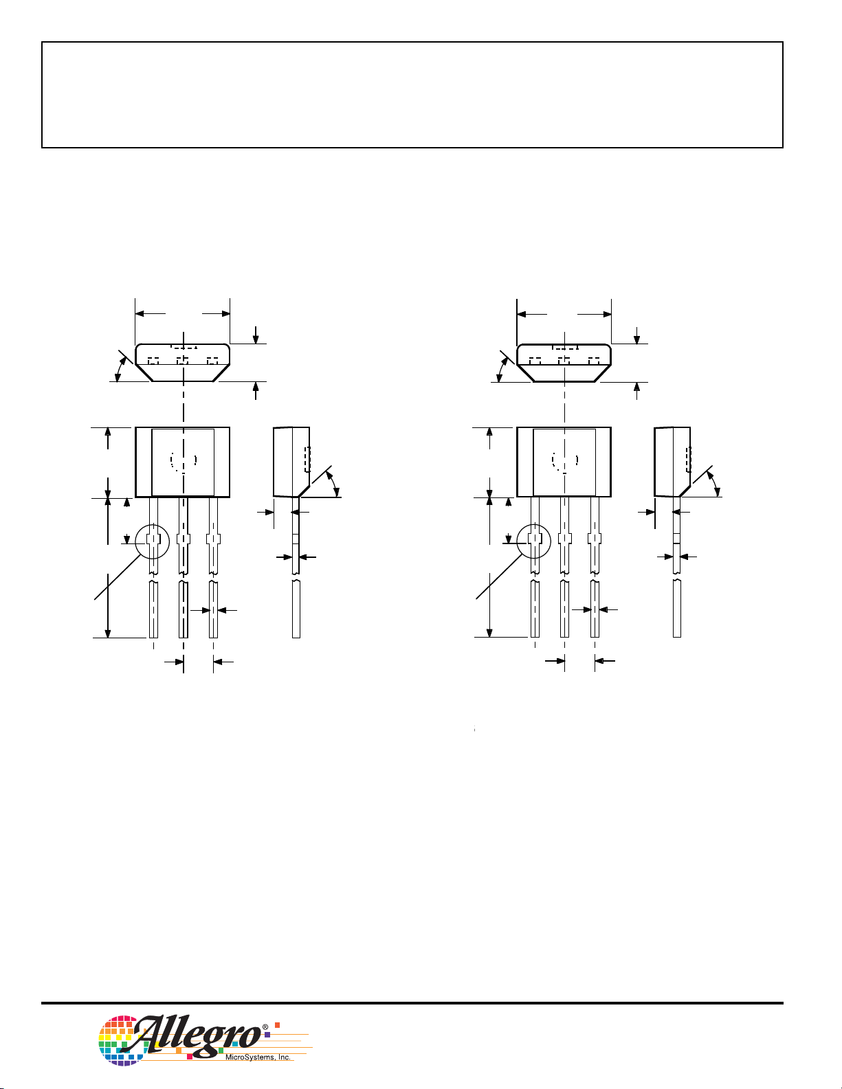
PACKAGE DESIGNATOR ‘UA’
Dimensions in Inches
(controlling dimensions)
Dimensions in Millimeters
(for reference only)
SEE NOTE
45°
0.122
0.117
0.640
0.600
0.085
123
MAX
0.164
0.159
0.050
BSC
0.062
0.058
0.031
0.0189
0.0142
0.0173
0.0138
Dwg. MH-014E in
45°
SEE NOTE
45°
3.10
2.97
16.26
15.24
2.16
123
MAX
4.17
4.04
1.27
BSC
1.57
1.47
45°
0.79
0.44
0.35
0.48
0.36
Dwg. MH-014E mm
NOTES: 1. Tolerances on package height and width represent
allowable mold offsets. Dimensions given are
measured at the widest point (parting line).
2. Exact body and lead configuration at vendor’s option
within limits shown.
3. Height does not include mold gate flash.
4. Recommended minimum PWB hole diameter to clear
transition area is 0.035" (0.89 mm).
5. Where no tolerance is specified, dimension is nominal.
6. Supplied in bulk pack (500 pieces per bag).
11
115 Northeast Cutoff, Box 15036
Worcester, Massachusetts 01615-0036 (508) 853-5000
R
Page 12

 Loading...