

Page 1

DJ - C7 T / E
Service Manual
CONTENTS
SPEC IFICATIONS
General.................................................................................2
Transmitter..................................................................
Receiver......................................................................
CIRCU IT D ISC RIPTION
1) Receiver System
2) Transmitter System................................................
3) M38268MCL069GP (XA1023)
.................................................... 3-5
..........................
SEM ICONDUCTOR DATA
1) NJM2070M (XA0210)
2) TC4W53FU (XA0348)
3) XC62HR3302MR (XA0519)...............................
4) BA4510FV (XA0537)
5) NJM2904V (XA0573)
6) TK10931V (XA0666)
7) BU9831F (XA0882)
8) uPC2771TB (XA0953)
9) uPC2757TB (XA0976)..........................................
10) BR24L32FV (XA1008)
11) BD4930FVE (XA1009)
12) MB15A01PFV1 (XA1010)..................................
13) XC6383A701MR (XA1012)
14) MM1438BW (XA1013)
15) TC75S51FU (XA1014)
16) Transistor, Diode and LED Outline Drawing
17) LCD Connection (A48A002X)
..................................................
.......................................
.........................................
.........................................
...........................................
.............................................
.........................................
........................................
........................................
................................
................................................
.................................................
........................... .........
.........
.........
........
7-9
.........
.........
..........10
.........
........
........
........
........
........
12
.........
........
.....
........
PARTS LIST
MAIN Unit
2
2
6
KEY Unit..........................................................................22-23
BATTERY Unit........................................................... 23
PTT Unit
ROTARY ENCODER Unit....................................... 23
Mechanical Parts........................................................ 23
Packing Parts............................................................... 23
..................................................................
..................................................................... 23
ADJUSTMENT
1) Required Test Equipment
10
10
10
11
11
11
12
12
12
13
13
14
14
15
16
2) Entering and Releasing the Adjustment Mode.... 25-28
PC BOARD V IEW
SCHEMATIC DIA G RAM .........................
BLOC K DIA G RAM
......................................
.......................................
....................................
.....
19-22
24
...
29-33
...
34-35
36
EX PLODED VIEW
1) Front View..............................................................
2) Rear View...............................................................
........
.........
17
18
ALINCO, INC.
Page 2
SPECIFICATIONS
General
Type
Transmitter Range
Receiving Range
Modulation F3E
Operating temperature
Frequency stability
Antenna impedance 50ohm unbalanced (SMA)
Supply Voltage 3.7 - 6.0VDC (External)
Ground method Negative ground
Transmit
Current drain
Dimensions (Projection exclusive)
Weight Approx. 102g (EBP-58N inclusive)
Receive
Battery Save Approx. 19mA
VHF 144.000 - 147.995MHz 144.000 - 145.995MHz
UHF 420.000 - 449.995MHz 430.000 - 439.995MHz
WFM 88.100 - 1.7.995MHz 87.500 - 107.995MHz
VHF 108.000 - 173.995MHz 144.000 - 145.995MHz
UHF 380.000 - 511.995MHz 430.000 - 439.995MHz
3.7V(EBP-58N): VHF Approx. 0.25A, UHF Approx. 0.30A
DJ - C7T DJ-C7E
-10 °C ~ 60°C (+14°F ~ +140°F)
-7 ~ +3 ppm
DC6.0V: VHF Approx. 0.28A, UHF Approx. 0.32A
Approx. 70mA
58 (w) x 96 (h) x 14.5 (d) mm
Transmitter
Type
Output power
Modulation System
Maximum Frequency Deviation +/- 5kHz
Spurious Emission
Microphone impedance
DC6.0V
EBP-58N equipped
DJ-C7T DJ-C7E
Approx. 0.5W
Approx. 0.3W
Variable reactance frequency modulation
- 60 dB c or less
Approx. 2kohm
Receiver
Type
Receiver circuit
Intermediate frequency
Sensitivity (12dB SINAD)
Audio output power
Spurious response
Squelch sensitivity
1st
2nd
144.000 - 147.995MHz
420.000 - 449.995MHz
100mW or more (Max) / 90mW or more (8ohm, 10 % THD)
DJ-C7T DJ-C7E
Double conversion super-heterodyne
50.85MHz (FM/AM), 10.7MHz (WFM)
450MHz (FM/AM)
-15dBu or less
60 dB or less
Approx. - 18 dBu or less
144.000 - 145.995MHz
430.000 - 439.995MHz
-15dBu or less
! NOTE: All specifications are subject to change without notice or obligation.
2
Page 3
CIRCUIT DESCRIPTION
1) Reception
1. RX M ethod
[FM/AM]
Double Super Heterodyne Method
1st IF: 50.85MHz
2nd IF: 450kHz
[WFM]
Single Super Heterodyne Method
1st IF: 10.7MHz
2. Fro nt End
[WFM BAND]
The signal input from antenna passes through the low pass filter, and then it is
amplified at RF amplifier Q13. The amplified signal is led to band pass filter
and band switch D17, then input to the mixer IC3.
[VHF BAND]
The signal input from antenna passes through the low pass filter, and then it is
amplified at RF amplifier Q18. The amplified signal is led to band pass filter
and band switch D17, then input to the mixer IC3.
3. M ixer
[UHF BAND]
The signal input from antenna passes through the band pass filter, and then it
is amplified at RF amplifier Q21. The amplified signal is led to band pass
filter and band switch D29, then input to the mixer IC3.
[FM/AM]
The input signal to the mixer IC3 and the 1st local signal are added or
subtracted at mixer IC3, and the crystal filter FL1 selects the signal of 50.85
MHz, then it is amplified at the 1st IF amplifier Q15 after the adjacent signal
is eliminated.
[WFM]
The input signal to the mixer IC3 and the 1st local signal are added or
subtracted at mixer IC3, and the ceramic filter FL2 selects the signal of
10.7MHz, then it is amplified at the 1st IF amplifier Q14 after the adjacent
signal is eliminated.
3
Page 4
4. IF
[FM/AM]
The signal amplified at the 1st IF amplifier Q15 is supplied to pin 24 of IC7
for demodulation. Also the signal of 12.6 MHz from the reference buffer
output of IC2 is multiplied by 3 at Q12, and then it is led to pin 1 of IC7. 2
input signals are mixed in the mixer circuit inside IC7 and converted into the
2nd IF signal of 450kHz.The converted 2nd IF signal is output from pin 3 of
IC7.
[FM]
The output signal from pin 3 of IC7 is led to pin 7 of IC7 after eliminating the
adjacent channel signal at the ceramic filter FL3. The input 2nd IF signal to
pin 7 of IC7 is demodulated at the limiter amplifier and quadrature detector
circuits inside of IC7, then output from pin 12 of IC7 as an AF signal.
[AM]
The output signal from pin 3 of IC7 is led to the pin 5 of IC7 after eliminating
the adjacent channel signal at the ceramic filter FL3. The 2nd IF signal input
to pin 5 of IC7 is AM-demodulated inside of IC and output from pin 13 of
IC7 as an AF signal. The 1st IF amplifier Q15 is controlled by reverse AGC at
AGC amplifier Q19 to get better audio output even though the input is
changed, and the gain is controlled.
[WFM]
The signal amplified at the 1st IF amplifier Q14 is supplied to pin 7 of IC7 for
demodulation.
The input 2nd IF signal to pin 7 of IC7 is demodulated at the limiter amplifier
and quadrature detector circuits inside of IC7, then output from pin 12 of IC7
as an AF signal.
5. Squelch
6. Audio
The AF signal got from pin 12 of IC7 is fed to pin 19 of IC7. The input signal
is output from pin 21 of IC7 passing through the noise filter amplifier and
rectifier circuits inside of IC7. The rectified signal is added to the A/D port of
the microcomputer IC6. Judging the signal, the microcomputer controls
ON/OFF of the audio output.
[FM/AM/WFM]
The selection of receiving audio output signal between FM/WFM and AM is
performed at IC8. The volume of output audio signal is adjusted at the
electronic volume IC14 via the AF amplifier Q27. The signal is input to pin 2
of audio power amplifier IC12 and output from pin 6 to drive a speaker, etc.
4
Page 5
7. VCO
8. P LL
[VHF]
VCO in VHF band consists of the Colpitts oscillator. D3, D4 and L11
determine the oscillating frequency, and the signal is oscillated at the
transistor Q2. The oscillated signal is supplied to pin 8 of PLL-IC2 passing
through the buffer amplifier Q5 and Q4.
[UHF]
VCO in UHF band consists of the Colpitts oscillator. D9, D11 and L18
determine the oscillating frequency, and the signal is oscillated at the
transistor Q7. The oscillated signal is supplied to pin 8 of PLL-IC2 passing
through the buffer amplifier Q5 and Q4.
PLL-IC2 is used to control the oscillating frequency of VCO. IC2 is
controlled by the serial control signal sent from the microprocessor IC6. The
12.6MHz reference frequency of IC2 oscillates the crystal oscillator X1 at the
inside circuit.
[VHF]
IC2 compares the frequency gained by dividing the signal added to pin 8 of
IC2 by the control signal from IC6 with the frequency gained by dividing the
reference frequency of 12.6MHz inside IC2. When the phase difference is
found as a result of phase comparison, the pulse signal is output from the
charge pump output of pin 5 of IC2, then the signal is converted into the DC
voltage at the passive filter and added to the cathode side of VCO
variable-capacitor D3 and D4 to make the phases equal. In result the
stabilized oscillation can be done at the desired frequency.
[UHF]
IC2 compares the frequency gained by dividing the signal added to pin 8 of
IC2 by the control signal from IC6 with the frequency gained by dividing the
reference frequency of 12.6MHz inside IC2. When the phase difference is
found as a result of phase comparison, the pulse signal is output from the
charge pump output of pin 5 of IC2, then the signal is converted into the DC
voltage at the passive filter and added to the cathode side of VCO
variable-capacitor D9 and D11 to make the phases equal. In result the
stabilized oscillation can be done at the desired frequency.
5
Page 6
2) Transmitter
1. M icrophone Amplifier
2. Power Amplifier
The microphone amplifier IC301 has 2 operational amplifiers. The voice is
converted into the electric signal through the microphone, and then supplied
to IC301. The input signal is amplified and pre-emphasized to be output.
[VHF]
The signal output from microphone amplifier is adjusted the maximum
frequency deviation at VR2. The adjusted signal is added to the cathode of
VCO variable-capacitor D4 for deviation to change the capacity of the
oscillation circuit resulting the FM deviation.
[UHF]
The signal output from microphone amplifier is adjusted the maximum
frequency deviation at VR1. The adjusted signal is added to the cathode of
VCO variable-capacitor D10 for deviation to change the capacity of the
oscillation circuit resulting the FM deviation.
The oscillated signal at VCO is supplied to the power amplifier Q3, passing
through buffer amplifier Q5, driver amplifier IC1. The power-amplified signal
is supplied to the antenna through the duplexer after the harmonics are
attenuated enough.
6
Page 7
oo o o oo
tr- 1 o o t r- 1 tr-1 ; . .
M M t o t o oo O i
o o m o o o o o o o o o o o
CNO CO ÜO '
WOO^CnOlSCOtDOi
Illlitlttll tlttttttttttt
H
o
HH
£
3
EL
O
o
3
3
ft
ñ
O
3
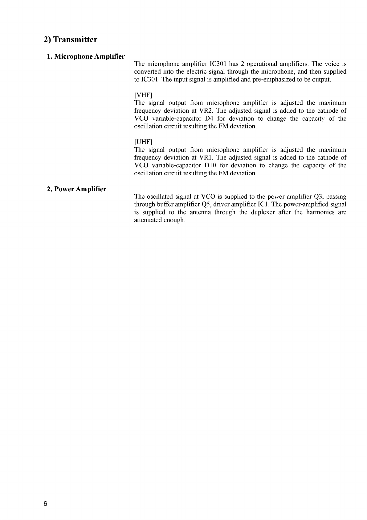
3) M38268MCL069GP (XA1023)
CPU
P67/AN7 -«—► [][
P66/AN6 -—^[2
P65/AN5 ■*—►[3
P64/AN4 ■*—►[J
P63/SCLK22/AN3 -*—*-[5
P62/SCLK21/AN2 -«—► [][
P61/S0UT2/AN 1 ——► [£
P60/SIN2/ANO •*—► [8
P57/ADT/DA2 -—^[9
P56/DA1 —— E
P55/CNTR1 -«—► [[]
P54/CNTRO -—►[H
P53/RTP1 -«—► [[3
P52/RTPO-«—►|I4
P51/PWM1 ■*—► [[5
P50/PWM0-*—►[IS
P47/SRDYT-«—► [17
P46/SCLK1 ——►[IS
P45/TXD -—►US
P44/RXD ——►|2C
P43/?i/TOUT -—►|2]
P42/INT2 -—^|22
P41/INT1 -—^|23
P40-—^|24
P77 -—►|25
O
—j —j — jrooo«O00C'0C'0C'0C'0C'0C'0C'0C'0i—i1
Q U i ^O O M h - O W — O Z d M S G ) U l ^ O O t \ 3 M O S
-SEG13
-SEG14
-SEG15
-SEG16
-SEG17
-P30/SEG18
-P31/SEG19
-P32/SEG20
-P33/SEG21
-P34/SEG22
-P35/SEG23
-P36/SEG24
-P37/SEG25
-P00/SEG26
-P01/SEG27
-P02/SEG28
-P03/SEG29
-P04/SEG30
-P05/SEG31
-P06/SEG32
-P07/SEG33
-P10/SEG34
-PI1/SEG35
-P12/SEG36
-P13/SEG37
CT5 cn hfca.
—I
Page 8
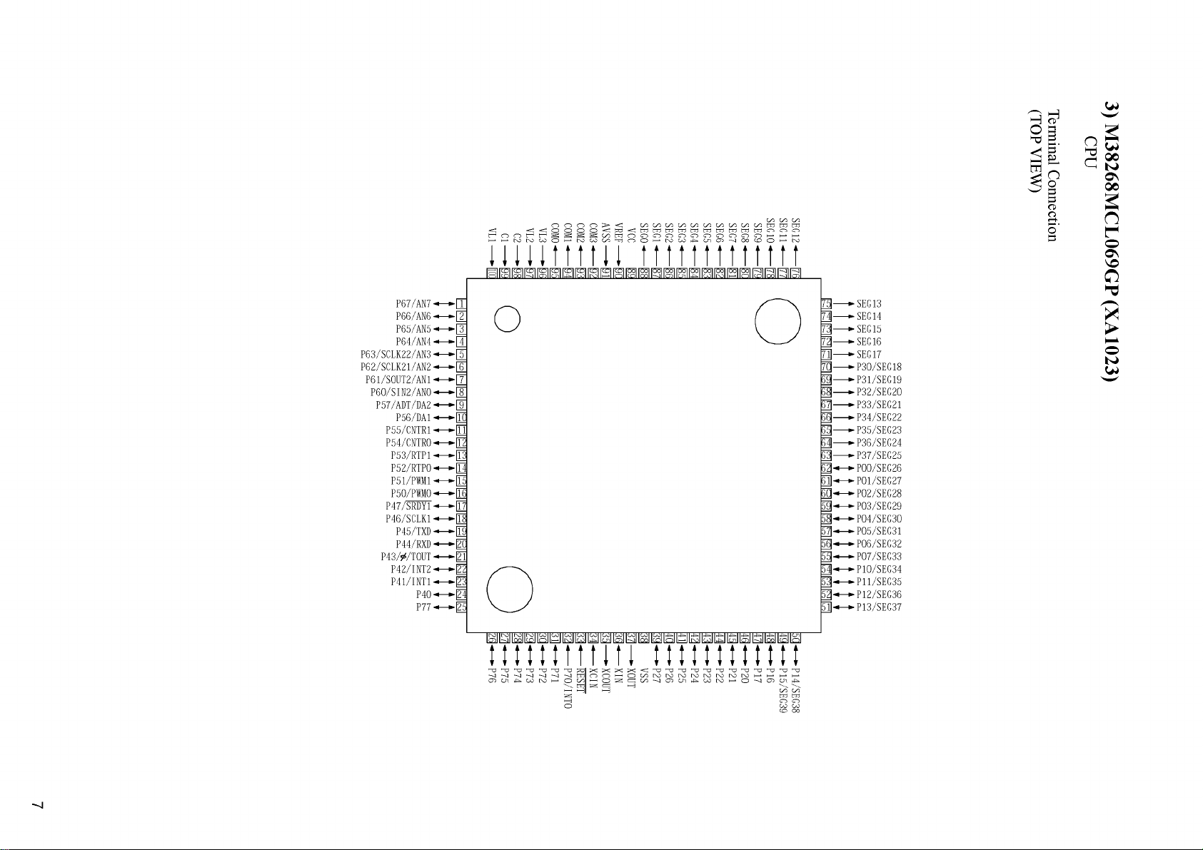
No. Terminal Signal I/O
Description
1 P67/AN7 BP1 I Band plan 1
2 P66/AN6 BCHK I Battery detection input
3 P65/AN5 PCNT 0 Battery detection SW output
4 P64/AN4 SMT I S-meter input
5 P63/SCLK22/AN3 SQL I
6 P62/SCLK21/AN2
7
P61/SOUT2/AN1 TLC O TX LED SW output
TIN
8 P60/SIN2/AN0 BAT I
9 P57/ADT/DA2 TUNC/TONE
10 P56/DA1
11 P55/CNTR1
PO O Power control output
C3C O
12 P54/CNTR0 TBST
13 P53/RTP1 PT3 I
14 P52/RTP0 CLK
15 P51/PWM1 DATA/UL
I/O Serial data output/Unlock input
16 P50/PWM0 STB1
17 P47/SRDY1 STB2
18 P46/SCLK1 EAR
19 P45/TXD CTX
20 P44/RXD CRX I
21 P43/p/TOUT BEEP/BP3
I/O Beep tone output/Band plan 3
I
O RX Tuning/Tone out
O Tone burst output
O Serial clock output
O Strobe for PLL
O Strobe for electronic volume
O Earphone antenna SW output
O Clone data transmission output
Noise level input for squelch
CTCSS Tone input
Battery charge voltage input
C3V power ON/OFF output
PTT input
Clone data reception input
22 P42/INT2 DET I DC-JACK detection input
23 P41/INT1 RE2 I Rotary encoder input 2
24 P40
RESW
I Rotary encoder push SW input
25 P77 RE1 I Rotary encoder input 1
26 P76
27 P75
28 P74
29 P73
30 P72 SDA
P3C O
PLC O Low VHF VCO ON/OFF output
PUC O
PVC O
I/O Serial data I/O for EEPROM
31 P71 SCL
32 P70/INT0
BU
33 RESET RESET I
34
35 XCOUT
36
XCIN NC
NC
XIN XIN
37 XOUT XOUT
38
VSS VSS
39 P27 V/M I
40 P26 BAND I
41 P25
SCAN
42 P24 POWER I
43 P23
44 P22
45 P21
46 P20
47 P17
48 P16
49 P15/SEG39
50 P14/SEG38
FUNC
MONI
BUG O Bugging SW output
CHG O Charge SW output
R3C O
BARC O Bar antenna SW output
BD1C O
BD2C O
O
I
— —
— —
I Clock input
O Clock output
—
I
I
I
PLL power ON/OFF output
UHF VCO ON/OFF output
VHF VCO ON/OFF output
Serial clock output for EEPROM
Back up signal detection input
Reset input
CPU GND
V/M key input
BAND key input
SCAN key input
POWER key input
FUNC key input
MONI key input
RX power ON/OFF output
BND1 power SW output
BND2 power SW output
8
Page 9
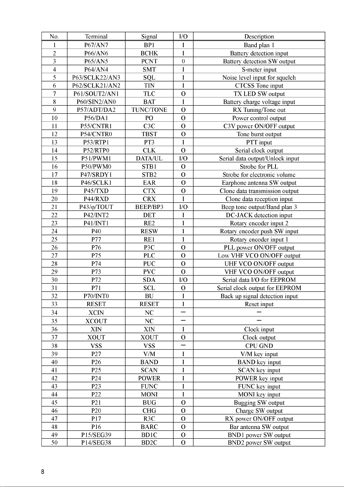
No. Terminal Signal I/O
51 P13/SEG37
52 P12/SEG36
53 P11/SEG35
54 P10/SEG34
55 P07/SEG33
56 P06/SEG32
57 P05/SEG31
58 P04/SEG30
59 P03/SEG29
60 P02/SEG28
61 P01/SEG27
W/NC O Wide / Narrow SW output
FMC O FM SW output
T3C O T3V power ON/OFF SW output
TSWC O Tone power ON/OFF SW output
TUC O
TVC O
BD3C O
BD4C O
AMC O AM SW output
AFC O AF SW output
AFPC O
62 P00/SEG26 SD
63 P37/SEG25 SEG25
64 P36/SEG24 SEG24
65 P35/SEG23 SEG23
66 P34/SEG22 SEG22
67 P33/SEG21 SEG21
68 P32/SEG20 SEG20
69 P31/SEG19 SEG19
70 P30/SEG18 SEG18
71 SEG17 SEG17
72 SEG16 SEG16
73 SEG15 SEG15
74 SEG14 SEG14
75 SEG13 SEG13
76 SEG12 SEG12
77
SEG11 SEG11 O LCD segment signal
78 SEG10 SEG10
79 SEG9 SEG09
80 SEG8 SEG8
81 SEG7 SEG7
82 SEG6 SEG6
83 SEG5 SEG5
84 SEG4 SEG4
85 SEG3 SEG3
86 SEG2 SEG2
87
SEG1 SEG1 O LCD segment signal
88 SEG0 SEG0
89
VCC
VDD
90 VREF VDD
91
AVSS
VDD
92 COM3 COM3
93 COM2 COM2
94 COM1 COM1
95 COM0 COM0
96 VL3 VL3
97 VL2 VL2
98 C2
99
C1 NC
NC
100 VL1 VL1
Description
UHF-TX power ON/OFF SW output
VHF-power ON/OFF SW output
BND3 power SW output
BND4 power SW output
AF power amp SW output
O
RX-LED ON/OFF SW output
O LCD segment signal
O LCD segment signal
O LCD segment signal
O LCD segment signal
O LCD segment signal
O LCD segment signal
O LCD segment signal
O LCD segment signal
O LCD segment signal
O LCD segment signal
O LCD segment signal
O LCD segment signal
O LCD segment signal
O LCD segment signal
O LCD segment signal
O LCD segment signal
O LCD segment signal
O LCD segment signal
O LCD segment signal
O LCD segment signal
O LCD segment signal
O LCD segment signal
O LCD segment signal
O LCD segment signal
—
—
—
O
O
O
O
—
—
CPU power supply
AD converter power supply
AD converter GND
LCD COM3 output
LCD COM2 output
LCD COM1 output
LCD COM0 output
LCD power supply
LCD power supply
— —
— —
—
LCD power supply
9
Page 10
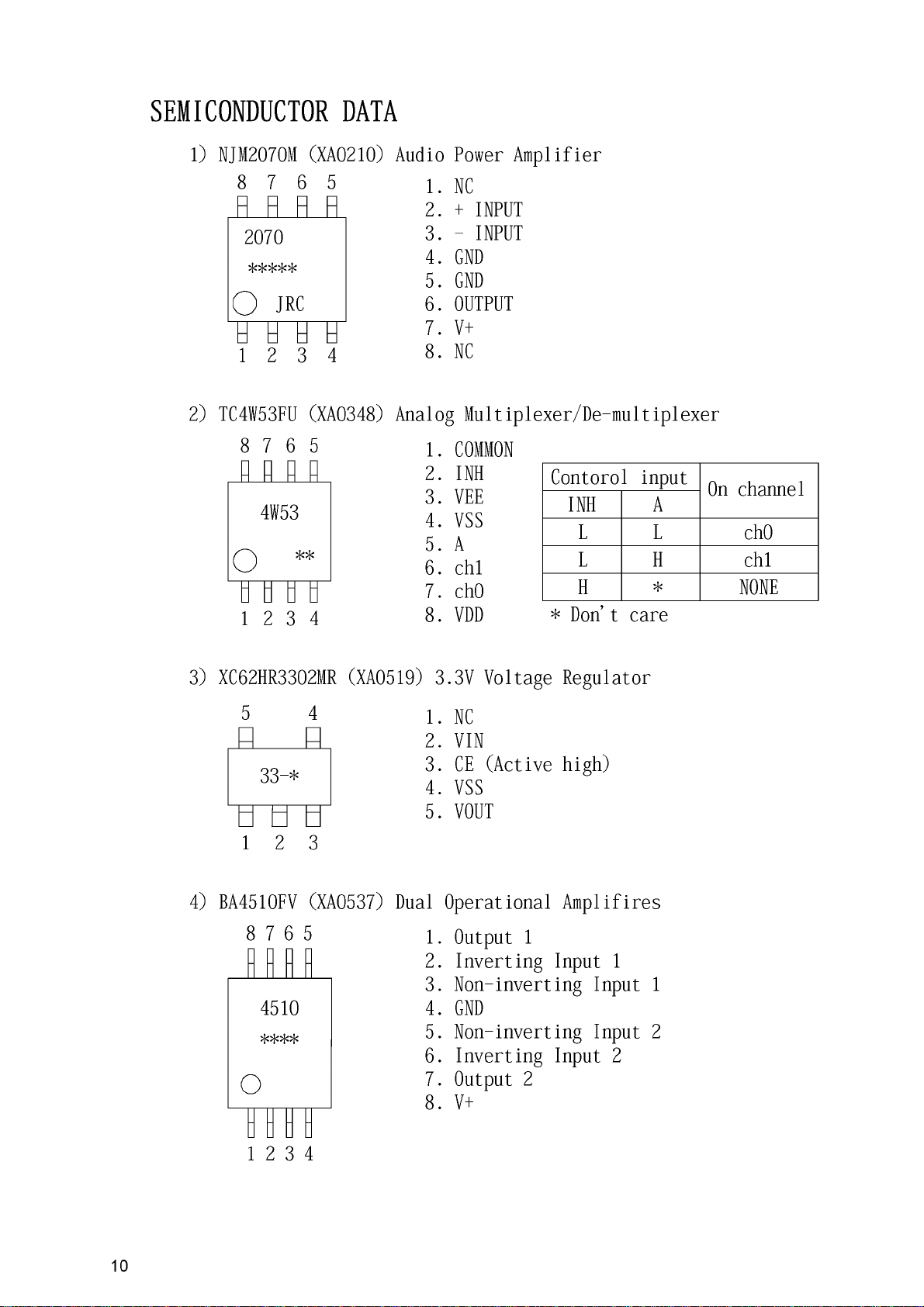
SEMICONDUCTOR DATA
1) NJM2070M (XA0210) Audio Power Amplifier
8 7 6 5
R H R R
O JRC
y y y y
1 2 3 4
2) TC4W53FU (XA0348) Analog Multiplexer/De-multiplexer
8 7 6 5 1. COMMON
W R W R 2. INH
□ □ □ □
1 2 3 4
1. NC
2. + INPUT
3. - INPUT
4. GND
5. GND
6. OUTPUT
7. V+
8. NC
3. VEE
4. VSS
5. A
6. ch1
7. ch0
8. VDD
Contorol input
INH A
L L
L H ch1
H
* Don’t care
*
On channel
ch0
NONE
3) XC62HR3302MR (XA0519) 3.3V Voltage Regulator
5
n
4) BA4510FV (XA0537) Dual Operational Amplifires
8 7 6 5
4
a
1. NC
2. VIN
3. CE (Active high)
4. VSS
5. VOUT
1. Output 1
2. Inverting Input 1
3. Non-inverting Input 1
4. GND
5. Non-inverting Input 2
6. Inverting Input 2
7. Output 2
8. V+
10
12 3 4
Page 11
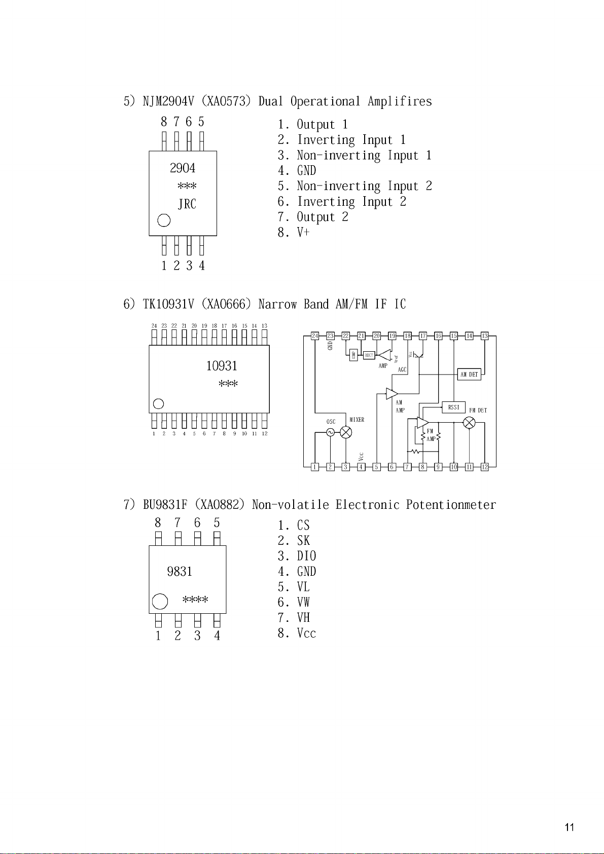
5) NJM2904V (XA0573) Dual Operational Amplifires
8 7 6 5 1. Output 1
2. Inverting Input 1
3. Non-inverting Input 1
4. GND
5. Non-inverting Input 2
6. Inverting Input 2
7. Output 2
8. V+
12 3 4
6) TK10931V (XA0666) Narrow Band AM/FM IF IC
24 23 22 21 20 19 18 17 16 15 14 13
10931
***
o
H M HFM m H H
1 2 3 4 5 6 7 8 9 10 11 12
7) BU9831F (XA0882) Non-volatile Electronic Potentionmeter
8 7 6 5 1 . CS
R R H R
2. SK
3. DIO
4. GND
5. VL
6. VW
F ¥ ¥ T 7. VH
1 2 3 4 8. Vcc
11
Page 12
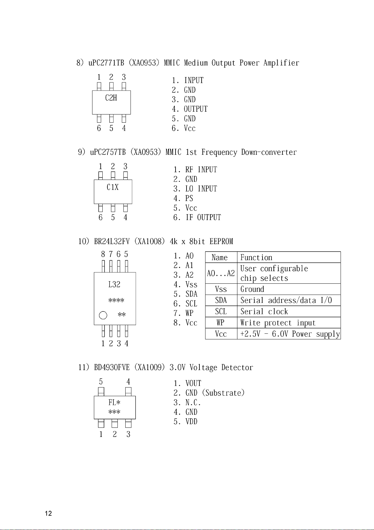
8) uPC2771TB (XA0953) MMIC Medium Output Power Amplifier
1 2 3
n n n
C2H
1. INPUT
2. GND
3. GND
4. OUTPUT
5. GND
6 5 4
6. Vcc
9) uPC2757TB (XA0953) MMIC 1st Frequency Down-converter
1 2 3
PPP
1. RF INPUT
2. GND
3. LO INPUT
4. PS
b b b
6 5 4
10) BR24L32FV (XA1008)
8 7 6 5
5. Vcc
6. IF OUTPUT
4k x 8bit EEPROM
1.
2.
3.
4.
5.
6.
7.
8.
A0
A1
A2
Vss
SDA
SCL
WP
Vcc
Name Function
A0...A2
Vss Ground
SDA
SCL Serial clock
WP Write protect input
User configurable
chip selects
Serial address/data I/O
12
Vcc +2.5V - 6.0V Power supply
1234
11) BD4930FVE (XA1009) 3.0V Voltage Detector
5
n
4
a
1. VOUT
2. GND (Substrate)
3. N.C.
4. GND
ü b ü
5. VDD
1 2 3
Page 13

12) MBlIAOlPFVl (XAlOlO) PLL Frequency Synthesizer
1G 1 I 14 iS 1 I 11 10 Q
1IA01
****
***
0
1.
OSC IN
2.
OSC OUT
Vp 12.
S.
4.
VCC iS. NC
I. Do
GND
G.
LD
I.
fin
S.
Q. Clock
10. Data
11. LE
FC
14.
fout
1I.
1G.
P
R
1 I S 4 I G I S
fr
fp
fr
fp
Mo nitor
freq u e ncy
sw itc h i n g
c i r c u i t
D i g i ta l loc k
dete c t o r
Phase
co m parator
FC
Ch arge pump
LD
J Í
Pro gra mma ble r e f e ren c e d i v id er
C ry s tal
O s c i l la to r
LE FC
Data
VCC
GND
Cot rol
1 b i t la tc h
P rescale r
G4/GI
H S /H Q
1
Binary 1 4 - b it
re f e r e n c e c o u n te r
1
__
M Ï Ï M
1 I - b i t la t c h
lQ -bit s h if t r e g i s t e r
lQ -bit s h if t r e g i s t e r
lS - b i t latc h
«^I - b it la tc h 11 -b it latc h
Pro gra mma ble d i v id e r
3=
Bin ar y I - b i t B in a ry 11-b i t
awallo w p rogra mma bl e
co u n te r cou n t er
Con tro l C ir c u i t
MC
fr
___
i::,
i
fp
LD
fo u t
Vp
Do
iS) XCGSSSAIOlMR (XA1012) PFM Controlled, Step-up DC/DC Converter IC
S
S .
HIO*
n
i 2
1. Vss
2. Lx
S. Vout
I.OV +/- 2.I/ output
13
Page 14

14) MM1438BW (XA1013) Litium-ion Battery Charging Control IC
8 7 6 5
n n n n
¥TT¥
1 2 3 4
15) TA75S51FU (XA1014) CMOS Singe Operational Amplifire
5
n n
o
b b b
1 2
4
SC
3
1. GND
2. LV
3. SW2
4. SW1
5. VCC
6. EXT
7. CEL
8. CS
1. Non-inverting Input
2. VSS
3. Inverting Input
4. Output
5. VDD
14
Page 15

16) Transistor, Diode and LED Outline Drawings
Top View
DAN235E
XD0320
n
M
u u
f t
MA781WK
XD0383
_n_
M2R
n u
n.
ö
n— er
2SK3078A
XE0049
UW
ü U U
G S D
MA2S357
XD0337
e| ts :
c—«— :
VDZT2R3.6B
XD0396
2
6
MCH6305
XE0058
DDS
n n n
JE
u u u
DDG
MA2S304
1SV311 1SV279
XD0343 XD0344 XD0364
4^ t3
m—:
MA72111
XD0397
t o
2SK3541
XE0059
D
X L
KN
UGT T
S
Í V1 h
c— :
DAN222M
"XD0400’
_n _
N
n u
Ji
ö
n er
SLM-521MUW
"XL0097”
F#§1
P3 Í
----Í Q
E E
R R
G
c— :
DG1M3
XD0401
2SC5066FT
XT0180
C
X L
M2
n u
B E
MA27077 MA27728
XD0381
■ IC
VDZT2R5.1B
’ "XD0402"'
cm
4
C—H-
XD0382
1 R t=
3SK274
XE0037
G2 G1
B
_ _
b g
D S
2SC4738
XT0181
2SC5609
XT0192
C
X L
I I
LL
TT
T T
rr
E
a
UN
C
3F
MCH6102 2SA2030 DTC144TM DTA123JM EMA8 EMD3 EMD6
XT0195
E
C
C
AB
u u u
C C B
XT0196 XU0205 XU0206 XU0207 XU0208 XU0209
C
n
BW
n u
B E
C
n
06
m n
B E B E
Rb=47kohl
Rbe=none
C
n
E32
m m
Rb=2.2kohl
Rbe=47kohl
CC
12
1A8
U ü ü
Rb=10kohl
Rbe=47kohl
CB
12
1 D3
ü ü u
Q_
o_
o_
Rb=10kohl
Rbe=10kohl
CB
12
d-
1D6
ü U ü
Rb=4.7kohl
Rbe=none
Cu
Cu
15
Page 16

17) LCD Connection (EL0056 A48A002X)
SEGMENT
"\
COMM ON
A
16
Page 17

EXPLODED VIEW
1) F ront View
17
Page 18

2) Rear View
18
Page 19

PARTS LIST
MAIN Unit
Ref
Parts No. D escriptio n P a rts Name Ve rsion
No.
FG0374 LCD RUBBER
FM0232 LCD FRAME
ST0082 LCD HOLDER DJC7
TS0174 VCO CASE DJC7
UP0497 PC Board C7 INTEGRATED
C1 CS0431 Chip Tantalum 10V 2.2UF
C2 CU3535 Chip C. GRM36B102K50PT
C3 CU3535 Chip C. GRM36B102K50PT
C4 CU3508 Chip C. 1005 CH 50V 7PF D
C5 CU3503 Chip C. GRM36CK020C50PT
C6 CU3535 Chip C. GRM36B102K50PT
C7 CU3535 Chip C. GRM36B102K50PT
C8 CS0396 Chip Tantalum 20V 0.1UF
C9 CU3535 Chip C. GRM36B102K50PT
C10 CU3535 Chip C. GRM36B102K50PT
C11 CS0429 Chip Tantalum 4V22UF
C12 CU3535 Chip C. GRM36B102K50PT
C13 CU3535 Chip C. GRM36B102K50PT
C14 CU3519 Chip C. GRM36CH470J50PT
C15 CU3509 Chip C. GRM36CH080D50PT
C17 CU3516 Chip C. GRM36CH270J50PT
C18 CU3517 Chip C. GRM36CH330J50PT
C20 CU3518 Chip C. GRM36CH390J50PT
C22 CU3507 Chip C. GRM36CH060D50PT
C23 CU3535 Chip C. GRM36B102K50PT
C24 CU3535 Chip C. GRM36B102K50PT
C25 CU3523 Chip C. GRM36CH101J50PT
C26 CU3502 Chip C. GRM36CK010C50PT
C27 CU3535 Chip C. GRM36B102K50PT
C28 CU3514 Chip C. GRM36CH180J50PT
C29 CU3502 Chip C. GRM36CK010C50PT
C30 CU3535 Chip C. GRM36B102K50PT
C31 CU3535 Chip C. GRM36B102K50PT
C32 CU3526 Chip C. GRM36CH181J25PT
C33 CU3527 Chip C. GRM36CH221J25PT
C34 CU3535 Chip C. GRM36B102K50PT
C35 CU3535 Chip C. GRM36B102K50PT
C36 CS0396 Chip Tantalum 20V 0.1UF
C37 CU3535 Chip C. GRM36B102K50PT
C38 CU3509 Chip C. GRM36CH080D50PT
C39 CU3512 Chip C. GRM36CH120J50PT
C40 CU3531 Chip C. GRM36B471K50PT
C41 CU3531 Chip C. GRM36B471K50PT
C42 CU3507 Chip C. GRM36CH060D50PT
C43 CU3518 Chip C. GRM36CH390J50PT
C44 CU3531 Chip C. GRM36B471K50PT
C45 CS0429 Chip Tantalum 4V22UF
C46 CU3502 Chip C. GRM36CK010C50PT
C47 CU3503 Chip C. GRM36CK020C50PT
C48 CU3508 Chip C. 1005 CH 50V 7PF D
C49 CU3512 Chip C. GRM36CH120J50PT
C50 CU3509 Chip C. GRM36CH080D50PT
C51 CU3527 Chip C. GRM36CH221J25PT
C52 CU3531 Chip C. GRM36B471K50PT
C53 CU3507 Chip C. GRM36CH060D50PT
C54 CU3535 Chip C. GRM36B102K50PT
C55 CU3512 Chip C. GRM36CH120J50PT
C56 CU3502 Chip C. GRM36CK010C50PT
C57 CU3509 Chip C. GRM36CH080D50PT
C58 CU3515 Chip C. GRM36CH220J50PT
C59 CU3535 Chip C. GRM36B102K50PT
C60 CS0396 Chip Tantalum 20V 0.1UF
C61 CU3503 Chip C. GRM36CK020C50PT
C62 CU3554 Chip C. GRM36B104K10PT
C63 CU3507 Chip C. GRM36CH060D50PT
Ref.
Pa rts No. D escriptio n P a rts Name Version
No.
C64 CU3515 Chip C. GRM36CH220J50PT
C67 CU3547 Chip C. GRM36B103K16PT
C68 CU3523 Chip C. GRM36CH101J50PT
C70 CU3531 Chip C. GRM36B471K50PT
C72 CU3535 Chip C. GRM36B102K50PT
C73 CU3535 Chip C. GRM36B102K50PT
C74 CS0396 Chip Tantalum 20V 0.1UF
C76 CS0431 Chip Tantalum 10V 2.2UF
C78 CU3547 Chip C. GRM36B103K16PT
C79 CS0429 Chip Tantalum 4V22UF
C80 CU3535 Chip C. GRM36B102K50PT
C83 CU3535 Chip C. GRM36B102K50PT
C84 CU3535 Chip C. GRM36B102K50PT
C85 CU3547 Chip C. GRM36B103K16PT
C86 CU3501 Chip C. GRM36CK0R5C50PT
C87 CU3547 Chip C. GRM36B103K16PT
C88 CU3506 Chip C. GRM36CH050C50PT
C89 CU3547 Chip C. GRM36B103K16PT
C91 CU3514 Chip C. GRM36CH180J50PT
C92 CU3503 Chip C. GRM36CK020C50PT
C93 CU3504 Chip C. GRM36CJ030C50PT
C94 CU3519 Chip C. GRM36CH470J50PT
C95 CU3518 Chip C. GRM36CH390J50PT
C96 CU3514 Chip C. GRM36CH180J50PT
C97 CU3535 Chip C. GRM36B102K50PT
C98 CU3511 Chip C. GRM36CH100D50PT
C99 CU3535 Chip C. GRM36B102K50PT
C100 CU3547 Chip C. GRM36B103K16PT
C101 CU3515 Chip C. GRM36CH220J50PT
C102 CU3517 Chip C. GRM36CH330J50PT
C103 CU3513 Chip C. GRM36CH150J50PT
C104 CU3517 Chip C. GRM36CH330J50PT
C105 CU3519 Chip C. GRM36CH470J50PT
C107 CU3509 Chip C. GRM36CH080D50PT
C108 CU3514 Chip C. GRM36CH180J50PT
C109 CU3522 Chip C. GRM36CH820J50PT
C110 CU3535 Chip C. GRM36B102K50PT
C111 CS0429 Chip C. 4V22UF
C112 CS0429 Chip Tantalum 4V22UF
C113 CU3535 Chip C. GRM36B102K50PT
C114 CU3535 Chip C. GRM36B102K50PT
C115 CU3519 Chip C. GRM36CH470J50PT
C116 CU3535 Chip C. GRM36B102K50PT
C117 CU3551 Chip C. GRM36B223K16PT
C118 CU3506 Chip C. GRM36CH050C50PT
C119 CU3535 Chip C. GRM36B102K50PT
C120 CU3554 Chip C. GRM36B104K10PT
C121 CU3535 Chip C. GRM36B102K50PT
C122 CU3535 Chip C. GRM36B102K50PT
C123 CU3515 Chip C. GRM36CH220J50PT
C124 CU3515 Chip C. GRM36CH220J50PT
C125 CU3519 Chip C. GRM36CH470J50PT
C126 CU3523 Chip C. GRM36CH101J50PT
C127 CU3523 Chip C. GRM36CH101J50PT
C128 CU3535 Chip C. GRM36B102K50PT
C130 CU3551 Chip C. GRM36B223K16PT
C131 CU3554 Chip C. GRM36B104K10PT
C132 CU3547 Chip C. GRM36B103K16PT
C133 CU3547 Chip C. GRM36B103K16PT
C134 CU3559 Chip C. GRM155B30J105KE18D
C135 CU3531 Chip C. GRM36B471K50PT
C136 CS0428 Chip Tantalum 4V15UF
C137 CU3551 Chip C. GRM36B223K16PT
C138 CU3535 Chip C. GRM36B102K50PT
C139 CU3513 Chip C. GRM36CH150J50PT
19
Page 20

Ref.
Parts No. D escriptio n P a rts Name
No.
C141 CU3531 Chip C. GRM36B471K50PT
C142 CU3531 Chip C. GRM36B471K50PT
C143 CU3506 Chip C. GRM36CH050C50PT
C144 CU3513 Chip C. GRM36CH150J50PT
C145 CS0432 Chip Tantalum TMCMA1A226MTR
C146 CS0425 Chip Tantalum TMCMBOJ107MTR
C147 CU3501 Chip C. GRM36CK0R5C50PT
C148 CU3506 Chip C. GRM36CH050C50PT
C149 CU3506 Chip C. GRM36CH050C50PT
C150 CU3519 Chip C. GRM36CH470J50PT
C151 CU3559 Chip C. GRM155B30J105KE18D
C152 CU3554 Chip C. GRM36B104K10PT
C153 CU3547 Chip C. GRM36B103K16PT
C154 CU3554 Chip C. GRM36B104K10PT
C155 CU3554 Chip C. GRM36B104K10PT
C156 CU3511 Chip C. GRM36CH100D50PT
C157 CU3519 Chip C. GRM36CH470J50PT
C158 CU3506 Chip C. GRM36CH050C50PT
C160 CU3535 Chip C. GRM36B102K50PT
C161 CU3554 Chip C. GRM36B104K10PT
C162 CU3523 Chip C. GRM36CH101J50PT
C163 CS0429 Chip Tantalum 4V22UF
C164 CU3547 Chip C. GRM36B103K16PT
C165 CU3559 Chip C. GRM155B30J105KE18D
C166 CU3547 Chip C. GRM36B103K16PT
C167 CU3531 Chip C. GRM36B471K50PT
C168 CU3547 Chip C. GRM36B103K16PT
C169 CU3554 Chip C. GRM36B104K10PT
C171 CU3535 Chip C. GRM36B102K50PT
C172 CU3517 Chip C. GRM36CH330J50PT
C173 CU3517 Chip C. GRM36CH330J50PT
C174 CS0425 Chip Tantalum TMCMBOJ107MTR
C175 CU3554 Chip C. GRM36B104K10PT
C176 CU3554 Chip C. GRM36B104K10PT
C177 CU3554 Chip C. GRM36B104K10PT
C178 CU3523 Chip C. GRM36CH101J50PT
C179 CS0431 Chip Tantalum 10V 2.2UF
C180 CU3559 Chip C. GRM155B30J105KE18D
C181 CU3554 Chip C. GRM36B104K10PT
C182 CS0425 Chip Tantalum TMCMBOJ107MTR
C183 CU3559 Chip C. GRM155B30J105KE18D
C184 CU3535 Chip C. GRM36B102K50PT
C185 CU3551 Chip C. GRM36B223K16PT
C186 CU3551 Chip C. GRM36B223K16PT
C187 CS0397 Chip Tantalum 16V 1UF
C188 CU3547 Chip C. GRM36B103K16PT
C189 CU3547 Chip C. GRM36B103K16PT
C190 CU3535 Chip C. GRM36B102K50PT
C191 CU3535 Chip C. GRM36B102K50PT
C192 CS0424 Chip Tantalum TMCMA1C106MTR
C193 CU3535 Chip C. GRM36B102K50PT
C194 CS0429 Chip Tantalum 4V22UF
C195 CU3559 Chip C. GRM155B30J105KE18D
C197 CU3547 Chip C. GRM36B103K16PT
C198 CU3501 Chip C. GRM36CK0R5C50PT
C199 CU3547 Chip C. GRM36B103K16PT
C200 CU3547 Chip C. GRM36B103K16PT
C201 CU3505 Chip C. GRM36CH040C50PT
C202 CU3512 Chip C. GRM36CH120J50PT
C204 CU3547 Chip C. GRM36B103K16PT
C205 CS0432 Chip Tantalum TMCMA1A226MTR
C206 CS0431 Chip Tantalum 10V 2.2UF
C207 CU3539 Chip C. GRM36B222K50PT
C208 CS0431 Chip Tantalum 10V 2.2UF
CN1 UE0474 C onnector AXK6F1 6545YJ
D1 XD0397 Chip Diode MA2711100L
D2 XD0381 Chip Diode MA27077
D3 XD0343 Chip Diode MA2S304001AR
D4 XD0343 Chip Diode MA2S304001AR
D5 XD0364 Chip Diode 1SV279-TPH3
D7 XD0381 Chip Diode MA27077
Vers ion
Ref.
Pa rts No. D escriptio n P a rts Name
No.
D8 XD0381 Chip Diode MA27077
D9 XD0364 Chip Diode 1SV279-TPH3
D10 XD0364 Chip Diode 1SV279-TPH3
D11 XD0364 Chip Diode 1SV279-TPH3
D14 XD0337 Chip Diode MA2S357-TX
D15 XD0337 Chip Diode MA2S357-TX
D16 XD0400 Chip Diode DAN222MT2L
D17 XD0320 Chip Diode DAN235E-TL
D18 XD0320 Chip Diode DAN235E-TL
D19 XD0381 Chip Diode MA27077
D20 XD0343 Chip Diode MA2S304001AR
D21 XD0343 Chip Diode MA2S304001AR
D23 XD0343 Chip Diode MA2S304001AR
D24 XD0344 Chip Diode 1SV311 TPH3
D25 XD0344 Chip Diode 1SV311 TPH3
D26 XD0344 Chip Diode 1SV311 TPH3
D27 XD0383 Chip Diode MA781WK-TX
D28 XD0381 Chip Diode MA27077
D29 XD0381 Chip Diode MA27077
D30 XD0382 Chip Diode MA27728
D31 XD0344 Chip Diode 1SV311 TPH3
D32 XD0400 Chip Diode DAN222MT2L
D33 XL0097 Chip LED SM L-521MUWT86
D34 XD0381 Chip Diode MA27077
D35 XD0401 Chip Diode DG1M3
D36 XD0397 Chip Diode MA2711100L
D37 XD0381 Chip Diode MA27077
D38 XD0381 Chip Diode MA27077
D42 XD0396 Chip Diode VDZT2R 3.9B
FL1 XF0062 Crystal Filter DSF444SAF 50.85MHZ
FL2 XC0097 Ceramic Filter SFECV10M7JA00-R0
FL3 XC0075 Ceramic Filter CFUCG450E-TC
IC1 XA0953 IC UPC2771TB-E3
IC2 XA1010 IC M B15A01PFV1-G-BND-EF
IC3 XA0976 IC UPC2757TB-E3
IC4 XA0519 IC XC62HR3302MR
IC5 XA1014 IC TC75S51FU TE85L
IC6 XA1011 IC CPU DJC7
IC7 XA0666 IC TK10931V
IC8 XA0348 IC TC4W53FU(TE12L)
IC9 XA1012 IC XC6383A701MR
IC11 XA1008 IC BR24L32FV-WE2
IC12 XA0210 IC IC NJM2070M
IC13 XA1009 IC BD4930FVE-TR
IC14 XA0882 IC BU9831F
JK1 UJ0054 Jack HSJ1 102-01-520
JK2 UJ0055 Jack HEC4306-010010
L1 QC0538 Chip Inductor LQN21AR10J04
L2 QC0507 Chip Inductor LK16081R 0K-T
L3 QC0587 Chip Inductor LQW1608A18NJ00T1
L4 QC0587 Chip Inductor LQW1608A18NJ00T1
L5 QC0591 Chip Inductor LQW1608A39NJ00T1
L6 QC0591 Chip Inductor LQW1608A39NJ00T1
L7 QC0589 Chip Inductor LQW1608A27NJ00T1
L8 QC0596 Chip Inductor LQW1608AR10J00T1
L9 QC0508 Chip Inductor LK16082R2K-T
L10 QC0617 Chip Inductor LL1608-FS15N J
L11 QC0594 Chip Inductor LQW1608A68NJ00T1
L12 QC0586 Chip Inductor LQW1608A15NJ00T1
L13 QC0586 Chip Inductor LQW1608A15NJ00T1
L14 QC0507 Chip Inductor LK16081R0K-T
L15 QC0586 Chip Inductor LQW1608A15NJ00T1
L16 QC0587 Chip Inductor LQW1608A18NJ00T1
L17 QC0507 Chip Inductor LK16081R0K-T
L18 QC0585 Chip Inductor LQW1608A12NJ00T1
L19 QC0716 Chip Inductor LQW1608AR27J00T1
L20 QC0709 Chip Inductor HK1005R10J
L22 QC0719 Chip Inductor LQW1608AR39J00T1
L23 QC0716 Chip Inductor LQW1608AR27J00T1
L25 QC0600 Chip Inductor LQW1608AR22J00T1
L26 QC0719 Chip Inductor LQW1608AR39J00T1
Version
20
Page 21

Ref.
Parts No. D escriptio n P a rts Name
No.
L27 QC0592 Chip Inductor LQW1608A47NJ00T1
L28 QC0718 Chip Inductor LQW1608AR33J00T1
L29 QC0597 Chip Inductor LQW1608AR12J00T1
L30 QC0720 Chip Inductor LQW1608AR47J00T1
L31 QC0598 Chip Inductor LQW1608AR15J00
L32 QC0597 Chip Inductor LQW1608AR12J00T1
L33 QC0586 Chip Inductor LQW1608A15NJ00T1
L34 QC0590 Chip Inductor LQW1608A33NJ00T1
L35 QC0590 Chip Inductor LQW1608A33NJ00T1
L36 QC0587 Chip Inductor LQW1608A18NJ00T1
L37 QC0717 Chip Inductor NLV32T-471JPF
L38 QC0586 Chip Inductor LQW1608A15NJ00T1
L39 QC0585 Chip Inductor LQW1608A12NJ00T1
L40 QA0160 Coil K5-S2/33331 PKI-0042
L41 QC0592 Chip Inductor LQW1608A47NJ00T1
L42 QA0159 Coil DET COIL QA0159
L43 QC0507 Chip Inductor LK16081R0K-T
L44 QC0717 Chip Inductor NLV32T-471JPF
L45 QC0508 Chip Inductor LK16082R2K-T
LCD1 EL0056 LCD LCD DJC7
XU0209 Chip Transistor EMD6T2R
Q1
Q2 XT0180 Chip Transistor 2SC5066FT-Y(TE85L)
Q3 XE0049 Chip FET 2SK3078A(TE12L)
Q4 XT0180 Chip Transistor 2SC5066FT-Y(TE85L)
XT0180 Chip Transistor 2SC5066FT-Y(TE85L)
Q5
Q6 XU0205 Chip Transistor DTC144TMT2L
XT0180 Chip Transistor 2SC5066FT-Y(TE85L)
Q7
Q8 XU0206 Chip Transistor DTA123JMT2L
XU0205 Chip Transistor DTC144TMT2L
Q9
Q11 XT0180 Chip Transistor 2SC5066FT-Y(TE85L)
Q12 XT0180 Chip Transistor 2SC5066FT-Y(TE85L)
Q13 XT0180 Chip Transistor 2SC5066FT-Y(TE85L)
Q14 XT0181 Chip Transistor 2SC4738-BL(TE85R)
Q15 XT0181 Chip Transistor 2SC4738-BL(TE85R)
Q16 XU0205 Chip Transistor DTC144TMT2L
Q17 XU0208 Chip Transistor EMD3T2R
Q18 XE0037 Chip FET 3SK274(TE85L)
Q19 XT0192 Chip Transistor 2SC5609
Q21 XT0180 Chip Transistor 2SC5066FT-Y(TE85L)
Q22 XU0208 Chip Transistor EMD3T2R
Q23 XU0206 Chip Transistor DTA123JMT2L
Q24 XU0206 Chip Transistor DTA123JMT2L
Q25 XU0206 Chip Transistor DTA123JMT2L
Q26 XU0208 Chip Transistor EMD3T2R
Q27 XT0192 Chip Transistor 2SC5609
Q28 XU0207 Chip Transistor EMA8T2R
Q29 XU0207 Chip Transistor EMA8T2R
Q30 XU0207 Chip Transistor EMA8T2R
Q31 XU0207 Chip Transistor EMA8T2R
Q32 XU0207 Chip Transistor EMA8T2R
Q33 XU0207 Chip Transistor EMA8T2R
Q34 XU0207 Chip Transistor EMA8T2R
Q35 XU0206 Chip Transistor DTA123JMT2L
Q36 XT0195 Chip Transistor MC H6102-TL
Q37 XU0205 Chip Transistor DTC144TMT2L
Q38 XU0205 Chip Transistor DTC144TMT2L
Q39 XT0196 Chip Transistor 2SA2030T2L
Q40 XU0206 Chip Transistor DTA123JMT2L
Q41 XU0205 Chip Transistor DTC144TMT2L
Q42 XE0059 Chip FET 2SK3541T2L
R1 RK3538 Chip R. 1005 1/16W 1.0K OHMJ
R2 RK3526 Chip R. 1005 1/16W 100 OHM J
R3 RK3530 Chip R. 1005 1/16W 220 OHM J
R4 RK3538 Chip R. 1005 1/16W 1.0K OHMJ
R5 RK3532 Chip R. 1005 1/16W 330 OHM J
R6 RK3547 Chip R. 1005 1/16W 5.6K OHMJ
R7 RK3562 Chip R. 1005 1/16W 100K OHMJ
R8 RK3530 Chip R. 1005 1/16W 220 OHM J
R10 RK3518 Chip R. 1005 1/16W 22 OHM J
R11 RK3550 Chip R. 1005 1/16W 10K OHM J
R12 RK3550 Chip R. 1005 1/16W 10K OHM J
Vers ion
Ref.
Pa rts No. D escriptio n P a rts Name Version
No.
R13 RK3530 Chip R. 1005 1/16W 220 OHM J
R14 RK3550 Chip R. 1005 1/16W 10K OHM J
R15 RK3536 Chip R. 1005 1/16W 680 OHM J
R16 RK3550 Chip R. 1005 1/16W 10K OHM J
R17 RK3542 Chip R. 1005 1/16W 2.2K OHMJ
R18 RK3550 Chip R. 1005 1/16W 10K OHM J
R19 RK3550 Chip R. 1005 1/16W 10K OHM J
R20 RK3530 Chip R. 1005 1/16W 220 OHM J
R21 RK3532 Chip R. 1005 1/16W 330 OHM J
R22 RK3544 Chip R. 1005 1/16W 3.3K OHMJ
R23 RK3546 Chip R. 1005 1/16W 4.7K OHMJ
R24 RK3526 Chip R. 1005 1/16W 100 OHM J
R25 RK3547 Chip R. 1005 1/16W 5.6K OHMJ
R26 RK3562 Chip R. 1005 1/16W 100K OHMJ
R27 RK3526 Chip R. 1005 1/16W 100 OHM J
R28 RK3530 Chip R. 1005 1/16W 220 OHM J
R29 RK3544 Chip R. 1005 1/16W 3.3K OHMJ
R30 RK3546 Chip R. 1005 1/16W 4.7K OHMJ
R31 RK3550 Chip R. 1005 1/16W 10K OHM J
R32 RK3550 Chip R. 1005 1/16W 10K OHM J
R33 RK3562 Chip R. 1005 1/16W 100K OHMJ
R34 RK3534 Chip R. 1005 1/16W 470 OHM J
R35 RK3550 Chip R. 1005 1/16W 10K OHM J
R36 RK3542 Chip R. 1005 1/16W 2.2K OHMJ
R37 RK3522 Chip R. 1005 1/16W 47 OHM J
R40 RK3544 Chip R. 1005 1/16W 3.3K OHMJ
R41 RK3542 Chip R. 1005 1/16W 2.2K OHMJ
R42 RK3562 Chip R. 1005 1/16W 100K OHMJ
R45 RK3539 Chip R. 1005 1/16W 1.2K OHMJ
R46 RK3526 Chip R. 1005 1/16W 100 OHM J
R47 RK3542 Chip R. 1005 1/16W 2.2K OHMJ
R48 RK3532 Chip R. 1005 1/16W 330 OHM J
R49 RK3548 Chip R. 1005 1/16W 6.8K OHMJ
R52 RK3542 Chip R. 1005 1/16W 2.2K OHMJ
R53 RK3538 Chip R. 1005 1/16W 1.0K OHMJ
R54 RK3529 Chip R. 1005 1/16W 180 OHM J
R55 RK3550 Chip R. 1005 1/16W 10K OHM J
R56 RK3534 Chip R. 1005 1/16W 470 OHM J
R57 RK3542 Chip R. 1005 1/16W 2.2K OHMJ
R58 RK3542 Chip R. 1005 1/16W 2.2K OHMJ
R59 RK3534 Chip R. 1005 1/16W 470 OHM J
R60 RK3562 Chip R. 1005 1/16W 100K OHMJ
R61 RK3542 Chip R. 1005 1/16W 2.2K OHMJ
R62 RK3542 Chip R. 1005 1/16W 2.2K OHMJ
R63 RK3562 Chip R. 1005 1/16W 100K OHMJ
R64 RK3566 Chip R. 1005 1/16W 220K OHMJ
R65 RK3526 Chip R. 1005 1/16W 100 OHM J
R66 RK3538 Chip R. 1005 1/16W 1.0K OHMJ
R67 RK3540 Chip R. 1005 1/16W 1.5K OHMJ
R68 RK3542 Chip R. 1005 1/16W 2.2K OHMJ
R69 RK3542 Chip R. 1005 1/16W 2.2K OHMJ
R70 RK3568 Chip R. 1005 1/16W 330K OHMJ
R71 RK3542 Chip R. 1005 1/16W 2.2K OHMJ
R72 RK3558 Chip R. 1005 1/16W 47K OHM J T
R73 RK3544 Chip R. 1005 1/16W 3.3K OHMJ
R74 RK3542 Chip R. 1005 1/16W 2.2K OHMJ
R75 RK3518 Chip R. 1005 1/16W 22 OHM J
R76 RK3542 Chip R. 1005 1/16W 2.2K OHMJ
R77 RK3558 Chip R. 1005 1/16W 47K OHM J E
R78 RK3550 Chip R. 1005 1/16W 10K OHM J
R79 RK3550 Chip R. 1005 1/16W 10K OHM J
R80 RK3550 Chip R. 1005 1/16W 10K OHM J
R81 RK3562 Chip R. 1005 1/16W 100K OHMJ
R82 RK3522 Chip R. 1005 1/16W 47 OHM J
R83 RK3562 Chip R. 1005 1/16W 100K OHMJ
R84 RK3561 Chip R. 1005 1/16W 82K OHM J
R85 RK3558 Chip R. 1005 1/16W 47K OHM J
R87 RK3550 Chip R. 1005 1/16W 10K OHM J
R88 RK3562 Chip R. 1005 1/16W 100K OHMJ
R89 RK3522 Chip R. 1005 1/16W 47 OHM J
R90 RK3562 Chip R. 1005 1/16W 100K OHMJ
21
Page 22

Ref.
Parts No. D escriptio n P a rts Name
No.
R91 RK3574 Chip R. 1005 1/16W 1.0M OHMJ
R92 RK3574 Chip R. 1005 1/16W 1.0M OHMJ
R93 RK3574 Chip R. 1005 1/16W 1.0M OHMJ
R94 RK3554 Chip R. 1005 1/16W 22K OHM J
R96 RK3554 Chip R. 1005 1/16W 22K OHM J
R97 RK3550 Chip R. 1005 1/16W 10K OHM J
R98 RK3554 Chip R. 1005 1/16W 22K OHM J
R100 RK3566 Chip R. 1005 1/16W 220K OHMJ
R101 RK3566 Chip R. 1005 1/16W 220K OHMJ
R102 RK3554 Chip R. 1005 1/16W 22K OHM J
R103 RK3556 Chip R. 1005 1/16W 33K OHM J
R104 RK3534 Chip R. 1005 1/16W 470 OHM J
R105 RK3559 Chip R. 1005 1/16W 56K OHM J
R106 RK3568 Chip R. 1005 1/16W 330K OHMJ
R107 RK3542 Chip R. 1005 1/16W 2.2K OHMJ
R109 RK3546 Chip R. 1005 1/16W 4.7K OHMJ
R110 RK3552 Chip R. 1005 1/16W 15K OHM J
R111 RK3542 Chip R. 1005 1/16W 2.2K OHMJ
R112 RK3562 Chip R. 1005 1/16W 100K OHMJ
R113 RK3538 Chip R. 1005 1/16W 1.0K OHMJ
R114 RK3574 Chip R. 1005 1/16W 1.0M OHMJ
R115 RK3574 Chip R. 1005 1/16W 1.0M OHMJ
R116 RK3574 Chip R. 1005 1/16W 1.0M OHMJ
R117 RK3574 Chip R. 1005 1/16W 1.0M OHMJ
R118 RK3550 Chip R. 1005 1/16W 10K OHM J
R119 RK3544 Chip R. 1005 1/16W 3.3K OHMJ
R120 RK3555 Chip R. 1005 1/16W 27K OHM J
R121 RK3542 Chip R. 1005 1/16W 2.2K OHMJ
R122 RK3554 Chip R. 1005 1/16W 22K OHM J
R123 RK3554 Chip R. 1005 1/16W 22K OHM J
R124 RK3538 Chip R. 1005 1/16W 1.0K OHMJ
R125 RK3527 Chip R. 1005 1/16W 120 OHM J
R126 RK3527 Chip R. 1005 1/16W 120 OHM J
R127 RK3554 Chip R. 1005 1/16W 22K OHM J
R128 RK3558 Chip R. 1005 1/16W 47K OHM J
R129 RK3542 Chip R. 1005 1/16W 2.2K OHMJ
R130 RK3538 Chip R. 1005 1/16W 1.0K OHMJ
R132 RK3562 Chip R. 1005 1/16W 100K OHMJ
R132 RK3562 Chip R. 1005 1/16W 100K OHMJ
R133 RK3534 Chip R. 1005 1/16W 470 OHM J
R134 RK3514 Chip R. 1005 1/16W 10 OHM J
R135 RK3562 Chip R. 1005 1/16W 100K OHMJ
R136 RK3562 Chip R. 1005 1/16W 100K OHMJ
R137 RK3526 Chip R. 1005 1/16W 100 OHM J
R138 RK3562 Chip R. 1005 1/16W 100K OHMJ
R139 RK3562 Chip R. 1005 1/16W 100K OHMJ
R141 RK3542 Chip R. 1005 1/16W 2.2K OHMJ
R142 RK3566 Chip R. 1005 1/16W 220K OHMJ
R143 RK3526 Chip R. 1005 1/16W 100 OHM J
R144 RK3501 Chip R. 1005 1/16W 0 OHM J
R145 RK3550 Chip R. 1005 1/16W 10K OHM J
R146 RK3554 Chip R. 1005 1/16W 22K OHM J
R147 RK3562 Chip R. 1005 1/16W 100K OHMJ
R148 RK3554 Chip R. 1005 1/16W 22K OHM J
R149 RK3566 Chip R. 1005 1/16W 220K OHMJ
R150 RK3538 Chip R. 1005 1/16W 1.0K OHMJ
R151 RK3562 Chip R. 1005 1/16W 100K OHMJ
R152 RK3550 Chip R. 1005 1/16W 10K OHM J
R153 RK3550 Chip R. 1005 1/16W 10K OHM J
R154 RK3554 Chip R. 1005 1/16W 22K OHM J
R155 RK3550 Chip R. 1005 1/16W 10K OHM J
R156 RK3559 Chip R. 1005 1/16W 56K OHM J
R157 RK3550 Chip R. 1005 1/16W 10K OHM J
R158 RK3550 Chip R. 1005 1/16W 10K OHM J
R159 RK3550 Chip R. 1005 1/16W 10K OHM J
R160 RK3538 Chip R. 1005 1/16W 1.0K OHMJ
R161 RK3562 Chip R. 1005 1/16W 100K OHMJ
R162 RK3550 Chip R. 1005 1/16W 10K OHM J
R163 RK3562 Chip R. 1005 1/16W 100K OHMJ
R164 RK3529 Chip R. 1005 1/16W 180 OHM J
R165 RK3526 Chip R. 1005 1/16W 100 OHM J
Vers ion
Ref.
Pa rts No. D escriptio n P a rts Name Version
No.
R167 RK3550 Chip R. 1005 1/16W 10K OHM J
R168 RK3542 Chip R. 1005 1/16W 2.2K OHMJ
R170 RK3574 Chip R. 1005 1/16W 1.0M OHMJ
R171 RK3536 Chip R. 1005 1/16W 680 OHM J
R172 RK3574 Chip R. 1005 1/16W 1.0M OHMJ
R173 RK3522 Chip R. 1005 1/16W 47 OHM J
R174 RK3522 Chip R. 1005 1/16W 47 OHM J
R175 RK3546 Chip R. 1005 1/16W 4.7K OHMJ
R176 RK3558 Chip R. 1005 1/16W 47K OHM J
R177 RK3558 Chip R. 1005 1/16W 47K OHM J
TC1 CT0050 Chip Trimmer TZY2Z100A001R00
VR1 RH0144 Chip Trimm er Pot 2720 22K OHM
VR2 RH0144 Chip Trimm er Pot 2720 22K OHM
W1 MRCL02AA Wire #30R02-20-02
X1 XQ0164 Crystal DSX321G 12.6MHZ
X2 XQ0132 Crystal CSA309/4.194304MHZ
KEY Unit
Ref.
Pa rts No. D escriptio n P a rts Name Version
No.
C301 CU3539 Chip C. GRM36B222K50PT
C302 CU3534 Chip C. 1005 B 50V 820PF K
C303 CU3539 Chip C. GRM36B222K50PT
C304 CU3559 Chip C. GRM155B30J105KE18D
C305 CU3521 Chip C. GRM36CH680J50PT
C306 CU3551 Chip C. GRM36B223K16PT
C307 CU3551 Chip C. GRM36B223K16PT
C308 CU3554 Chip C. GRM36B104K10PT
C309 CU3559 Chip C. GRM155B30J105KE18D
C310 CS0428 Chip Tantalum 4V15UF
C311 CU3535 Chip C. GRM36B102K50PT
C312 CU3554 Chip C. GRM36B104K10PT
C313 CU3552 Chip C. GRM36B333K10PT
C314 CU3537 Chip C. 1005 B 50V 0.0015UFK
C315 CU3552 Chip C. GRM36B333K10PT
C316 CU3554 Chip C. GRM36B104K10PT
C317 CU3523 Chip C. GRM36CH101J50PT
C318 CU3554 Chip C. GRM36B104K10PT
C319 CU3535 Chip C. GRM36B102K50PT
C320 CU3031 Chip C. 1608 B 50V 470PF K
CN301 UE0475 Connector AXK5F1 6545YJ
D301 XD0402 Chip Diode VDZT2R 5.1 B
IC301 XA0537 IC BA4510FV-E2
IC302 XA0573 IC NJM2904V-TE1
MIC301 EY0021 Mic SKB-1144SP-C1033
R301 RK3554 Chip R. 1005 1/16W 22K OHM J
R302 RK3558 Chip R. 1005 1/16W 47K OHM J
R303 RK3556 Chip R. 1005 1/16W 33K OHM J
R304 RK3554 Chip R. 1005 1/16W 22K OHM J
R305 RK3569 Chip R. 1005 1/16W 390K OHMJ
R306 RK3562 Chip R. 1005 1/16W 100K OHMJ
R307 RK3550 Chip R. 1005 1/16W 10K OHM J
R308 RK3534 Chip R. 1005 1/16W 470 OHM J
R309 RK3557 Chip R. 1005 1/16W 39K OHM J
R310 RK3556 Chip R. 1005 1/16W 33K OHM J
R311 RK3566 Chip R. 1005 1/16W 220K OHMJ
R312 RK3552 Chip R. 1005 1/16W 15K OHM J
R313 RK3557 Chip R. 1005 1/16W 39K OHM J
R314 RK3550 Chip R. 1005 1/16W 10K OHM J
R315 RK3550 Chip R. 1005 1/16W 10K OHM J
R316 RK3554 Chip R. 1005 1/16W 22K OHM J
R317 RK3574 Chip R. 1005 1/16W 1.0M OHMJ
R318 RK3538 Chip R. 1005 1/16W 1.0K OHMJ
R319 RK3561 Chip R. 1005 1/16W 82K OHM J
R320 RK3561 Chip R. 1005 1/16W 82K OHM J
R321 RK3561 Chip R. 1005 1/16W 82K OHM J
R322 RK3538 Chip R. 1005 1/16W 1.0K OHMJ
R323 RK3574 Chip R. 1005 1/16W 1.0M OHMJ
22
Page 23

Ref.
Parts No. D escriptio n P a rts Name V ers ion
No.
R324 RK3538 Chip R. 1005 1/16W 1.0K OHMJ
R325 RK3538 Chip R. 1005 1/16W 1.0K OHMJ
R326 RK3559 Chip R. 1005 1/16W 56K OHM J
R327 RK3538 Chip R. 1005 1/16W 1.0K OHMJ
R328 RK3572 Chip R. 1005 1/16W 680K OHMJ
R329 RK3570 Chip R. 1005 1/16W 470K OHMJ
R330 RK3563 Chip R. 1005 1/16W 120K OHMJ
R331 RK3574 Chip R. 1005 1/16W 1.0M OHMJ
R332 RK3526 Chip R. 1005 1/16W 100 OHM J
SW301 UU0027 Chip Switch SKQGAA
SW302 UU0027 Chip Switch SKQGAA
SW303 UU0027 Chip Switch SKQGAA
SW304 UU0027 Chip Switch SKQGAA
SW305 UU0027 Chip Switch SKQGAA
BATTERY Unit
Ref.
Parts No. D escriptio n P a rts Name V ers ion
No.
UE0476 CONTACT PIN
C401 CU3535 Chip C. GRM36B102K50PT
C402 CS0427 Chip Tantalum 6.3V10UF
D401 XD0401 Chip Diode DG1M3
IC401 XA1013 IC MM1438BWLE/R59-3644
Q401 XE0058 Chip FET MCH6305-TL
Q402 XT0195 Chip Transistor MCH6102-TL
Q403 XU0205 Chip Transistor DTC144TMT2L
R401 RK3562 Chip R. 1005 1/16W 100K OHMJ
R402 RK3550 Chip R. 1005 1/16W 10K OHM J
R403 RK3528 Chip R. 1005 1/16W 150 OHM J
R404 RK3562 Chip R. 1005 1/16W 100K OHMJ
R405 RK0159 Chip R. 1608 1/10W 0.33OHM J
PTT Unit
Ref.
Parts No. D escriptio n P a rts Name V ers ion
No.
SW501 UU0027 Chip Switch SKQGAA
SW502 UU0027 Chip Switch SKQGAA
ROTARY ENCODER Unit
Ref.
Parts No. D escriptio n P a rts Name V ers ion
No.
RE501 UR0023 Rotary Encoder TP70N00AE20 13.5F
Mechanical Unit
Ref.
Pa rts No. D escriptio n P a rts Name Version
No.
AF0032 OPH17+3 FE N3
AF0033 OPH P17+3 FE/BZN3
AN0012 RND N7X0.75 BR/B.ZN
AX0006 OPH P1.7+5.5 FE/BZN3
DP0163 LCD PANEL
ES0030 Speaker 28-8AB-09D
FG0375 ON AIR RUBBER
FG0376 PTT RUBBER
FM0233 ANTENNA GND DJC7
FP0238 FRONT COVER
FP0239 KEY TOP
FP0241 REAR COVER DJC7
KB0096 REAR CASE
KZ0172 FRONT ASSY DJC7
NK0080 KNOB
SP0013 KNOB SPRING 7800
UE0466 SMA ANTENNA CONNECT.
YX0035 LCD TAPE DJC7
YZ0135 SOLDER PLATED LINE 0.4-1 mm
Packing Unit
Ref.
Pa rts No. D escriptio n P a rts Name Version
No.
DS0446 SPEC. SHEET
EA0116 SMA ANTENNA
EDC126 AC ADAPTOR T
EDC128 AC ADAPTOR E
EG0055 EBP-58N PROTECTION BAG
FG0309 ANTENNA CAP
HK0598 Package
HM0235 CARTON 10
HP0003 PROTECTION BAG
HP0006Z PROTECTION BAG
HU0197 INNER 10
HU0209 INNER
PH0015A WARRANTY T
PK0102 CIRCUIT DIAGRAM
PR0447 FCC WARNING LABEL T
PR0452 FCC HOME USE LABEL T
PR0478 SERIAL SEAL E
PR0514 E-10x49 LABEL
PS0464 INSTRUCTION
PR0514 E-10x49 LABEL
PS0464 INSTRUCTION
23
Page 24

ADJUSTMENT
1) R equired Test Equipm ent
The following items are required to adjust radio parameters.
1. Regulated Power Supply
Supply voltage: 6.0VDC
Current:
2. Digital M ultim eter
Voltage range: FS = Approx. 20V
Current:
Input resistance: High impedance
3. Oscilloscope
Measurable frequency:
i
1
Impedance:
Dissipation:
Jack: 2.5$
5. SSG
Output frequency:
Output level:
Modulation:
6. Spectrum A nalyzer
Measuring range:
7. Power m eter
Measurable frequency:
Impedance: 50ft unbalanced
Measuring range: 0.1W to 1W
8. A udio Voltmeter
Measurable frequency: Up to 100kHz
Sensitivity: 1mV to 10V
9. A udio G enerator
Output frequency:
Output impedance: 600ft unbalanced
SINAD M eter
Measurable frequency:
Input level: Up to 40dB
Distortion level:
11. Frequency C ounter
12. L inear D etector
r
Measurable frequency:
Measurable stability:
Measurable frequency:
Characteristics: Flat
CN:
1A or more
10A or more
Audio Frequency
8ft
1W or more
500MHz or more
-20dB^ / 0.1^V to 120dB^ / 1V
FM / AM
Up to 2GHz or more
Up to 500MHz
67Hz to 10kHz
1kHz
1% to 100%
Up to 500MHz
Approx. ± 0.1ppm
Up to 500MHz
60dB or more
Note
• Standard modulation:
• Reference sensitivity:
• Specified audio output level:
• Standard audio output level:
• Use an RF cable (3D2W : 47cm ) for test equipment.
• Attach a fuse to RF indicated by EMF.
• All SSG outputs are indicated by EMF.
• Supply voltage for the transceiver: 6.0VDC
24
1kHz ± 3.5kHz I DEV
12dB SINAD
2GGmW at SQ
5GmW at SQ
Page 25

2) Entering and Releasing the Adjustment Mode
The DJ-C7 does not require a serviceperson to manipulate the components on the printed-circuit board, except
the trimmer when adjusting reference frequency and deviation. Most of the adjustments for the transceiver are
mode by using the keys on it while the unit is in the adjustment mode. Because the adjustment mode
temporarily uses the channels, frequency must be set on each channel before adjustments can be mode. For
instructions on how to program the channels, see the “DJ-C7 INSTRUCTION MANUAL” which came with the
product. In consideration of the radio environment, the frequency on each channel must be near the value
(+/-1MHz) listed in the table below. To enter the adjustment mode, set key lock and press [BAND], [V/M],
[SCAN], [V/M], [SCAN], [BAND], and [FUNC] key. “Freq” appears in LCD. When changing the adjustment
parameters, press the [SCAN] or [BAND] key.
To exit the adjustment mode, press the [MONI] key.
Adjustment Points
Fr on t sid e
Rear side
DC JACK
MIC/EAR JACK
tJHMJHUHUH
L40 :
o
L42
o
D
o
o
■D
“ U -
VR1Ü TC1©
25
Page 26

Set power supply voltage to 6.0V.
1. Reference frequency adju stm ent
Display: FrEq, Adjust point: TC1
Adjust the TC1 to 435.03MHz (C7E).
Adjust the TC1 to 445.03MHz (C7T).
2. UHF-Power adjustm ent
Display: U Pow, Adjust point: RE (Rotary Encoder)
Adjust the UHF-Power to 480mW at the TX condition.
Frequency: 435.03MHz (C7E)
Frequency: 445.03MHz (C7T)
3. VHF-Pow er adjustm ent
Display: v Pow, Adjust point: RE
Adjust the VHF-Power to 480mW at the TX condition.
Frequency: 145.03MHz
4. UHF-M odulation adjustm ent
Display: U mod, Adjust point: VR1
Input the low frequency of 1kHz 50mV from MIC terminal, and then adjust the modulation to 4.5kHz at the
TX condition.
Frequency: 435.03MHz (C7E)
Frequency: 445.03MHz (C7T)
5. V HF-M odulation adjustm ent
Display: v mod, Adjust point: VR2
Input the low frequency of 1kHz 50mV from MIC terminal, and then adjust the Modulation to 4.5kHz at the
TX condition.
Frequency: 145.03MHz
6. NFM -AF output adju stm ent
Display: nAF, Adjust point: L42
Input 80dBu to the test unit which modulation is 1kHz 3.5kHz and adjust the L42 to maximum AF level.
Frequency: 435.07MHz (C7E)
Frequency: 445.07MHz (C7T)
7. W FM -AF output adjustm ent
Display: wAF, Adjust point: L40
Input 80dBu to the test unit which modulation is 1kHz 22.5kHz and adjust the L40 to maximum AF level.
Frequency: 88.7MHz
8. V HF-Sensitivity ad justment
Adjust point: RE
Adjust the sensitivity to the best condition of 12dB SINAD.
Display: vL tUn Low-F sensitivity adjustment 118.07MHz
Display: vm tUn Mid-F sensitivity adjustment 145.07MHz
Display: vH tUn Hight-F sensitivity adjustment 165.07MHz
9. UHF-Sensitivity adjustm ent
Adjust point: RE
Adjust the sensitivity to the best condition of 12dB SINAD.
Display: UL tUn Low-F Sensitivity Adjustment 380.07MHz
Display: Um tUn Mid-F Sensitivity Adjustment 435.07MHz(C7E)
Mid-F Sensitivity Adjustment 445.07MHz(C7T)
Display: UH tUn Hight-F Sensitivity Adjustment 465.07MHz
26
Page 27

10. VHF-SQL ad justm ent
SQL MIN level Adjustment
Display: SqL vL Adjust point: [V/M] key
Input the 145.07MHz of -11dBu which modulation is 3.5kHz, and press the [V/M] key. Check the
BEEP sound.
SQL MAX level Adjustment
Display: SqL vH Adjust point: [V/M] key
Input the 145.07MHz of -3dBu which modulation is 3.5kHz, and press the [V/M] key. Check the
BEEP sound.
11. VHF S-m eter adjustm ent
S meter 1 level Adjustment.
Display: S vL Adjust point: [V/M] key
Input the 145.07MHz of -3dBu which modulation is 3.5kHz, and press the [V/M] key.
Check the BEEP sound.
Display: S vH S meter 5 level Adjustment.
Input the 145.07MHz of 12dBu which modulation is 3.5kHz, and press the [V/M] key. Check the
BEEP sound.
12. UHF SQL adjustm ent
SQL MIN level adjustment
Display: SqL UL Adjust point: [V/M] key
Input -10dBu which modulation is 3.5kHz, and press the [V/M] key.
Check the BEEP sound.
Frequency: 435.07MHz (C7E)
Frequency: 445.07MHz (C7T)
SQL MAX level adjustment
Display: SqL UH. Adjust point: [V/M] key
Input -2dBu which modulation is 3.5kHz, and press the [V/M] key.
Check the BEEP sound.
13. UHF S-m eter adju stm ent
S-meter 1 level adjustment
Display: S UL Adjust point: [V/M] key
Input -3dBu which modulation is 3.5kHz, and press the [V/M] key.
Check the BEEP sound.
Frequency: 435.07MHz (C7E)
Frequency: 445.07MHz (C7T)
S-meter 5 level adjustment
Display: S UH Adjust point: [V/M] key
Input 12dBu which modulation is 3.5kHz, and press the [V/M] key.
Check the BEEP sound.
14. W FM SQL adjustm ent
SQL MIN level Adjustment
Display: SqL wL Adjust point: [V/M] key
Input -2dBu which modulation is 22.5kHz, and press the [V/M] key.
Check the BEEP sound.
Frequency: 88.7MHz
SQL MAX level Adjustment
Display: SqL wH Adjust point: [V/M] key
Input 8dBu which modulation is 22.5kHz, and press the [V/M] key.
Check the BEEP sound.
27
Page 28

15. W FM S-m eter adjustment
S-meter 1 level Adjustment
Display: S wL Adjust point: [V/M] key
Input 5dBu which modulation is 22.5kHz, and press the [V/M] key.
Check the BEEP sound.
Frequency: 88.7MHz
S meter 5 level Adjustment
Display: S wH Adjust point: [V/M] key
Input 20dBu which modulation is 22.5kHz, and press the [V/M] key.
Check the BEEP sound.
16. Low B attery Display Setting
Display: bAtt Adjust point: [V/M] key
Set power supply voltage to 3.7V.
After that, press the [V/M] key.
Check the BEEP sound.
28
Page 29

PC Board View
MAIN Side A
VCO CASE(TS0174)
29
Page 30

MAIN Side B
p *s
TP5 C200
«4 n*D
■* nm
TP4 Cl 99
¡11 SI
R125
O
R87
o
cpflpfTon
C i Q
02 3
I I
L20
[Ml
fTvTlLtS
1=1 n°TIC10Q
y rToTIClB8
8
■L-r s B a ll d S E D C13 7 rm _ rr
- - , m^m S Si ^ gn 0
w Kj |C13B| R87 ^ 4— ^ Cl 18 m
" " I n—n
I I S ° OR86 D28a|3R
o O O RS R107
RL01 R103 a o
U J ;
C1 0 0 aan?'“ _n_,
t®] s i B g
CL33 ,
[M l
------
— ,— " h [HH
R102 CZO H O
n - n ™ 7 “ “
RRRRRRHRRRHH *
R97
yyyyyyyyyyyy g i
i r® is
uci5eo Sed
R110
C100
lloll
ra7 rrvru.
to
Clio
am c]||iei|3 OR58
& J=] DzD*
___
, d d 1=1«
J TPin
D
Dig
<y|<
B n 1 1!
C103
c !
5 0 ra§& C B fip-12
& ^ w 1 ¿ s| I
_ rrsn u*n a y° C33
E D
D QvE §11 1®£ 5?
"’inra inbpz n31C51 ^
C31ITon
=\ jr w p >O T
fc J ljU J t , ^ t k j
o
R11 2
o
LUJ
a
M M
u y y y
ICS
w v 15, g % ¡ s
o
r TPS0 t i H r p i
,ot^R1 54
<jip <sU y
J t ? IB ° J m 0 9 sBg
“0^082 y n- B
¡e « & b J &=?
OZD
R51
si CvD-^om
VRL„ ^ IO
U -U R29 O R 3 0 J E l
----
O
w
X2
I t
— *s7 ----------------------------------
T " No g a p
le s s th a n 1mm
^iCLhg<
R21
OZD
B 8 E
C37 11B
O [M l w
R27 C58 O
C73
[M l
R4L
30
Page 31

PC Board View
KEY Side A
31
Page 32

KEY Side B
32
Page 33

ROTARY ENCODER Side A & B
Page 34

PTT Side A & B
w
5
H
m
BATTERY Side A
s
05
a
re
Cd
Page 35

SCHEMATIC DIAGRAM
KEY UNIT
BATTERY UNIT
Li-ion
Battery
TP407
GND
r
34
Page 36

MAIN UNIT
|
______
MONI SWl
PTT PCB
35
Page 37

BLOCK DIAGRAM
ANT
36
Page 38

ALINCO, INC.
Head Office: Shin-Dai Building 9th Floor
2-6, 1-Chome, Dojimahama, Kitaku, Osaka 530-0004, Japan
Phone: +81-6-4797-2136 Fax: +81-6-4797-2157
E-mail: export@alinco.co.jp
Dealer/Distributor
Copyright 2004 Alinco, Inc. Osaka Japan
Printed in Japan PM0080
 Loading...