

Page 1
DJ-596T / DJ-596 E
Service Manual
CONTENTS
SPEC IFICATIO NS
1) GE NE R AL .............................................................................2
2) TR AN SM ITTER...................................................................2
3) RE CEIVE R
CIRCUIT D ESCRIPTION
1) [R X ]....................................................................................3~5
2) [TX ]..........................................................................................5
3) M 38267M8L(XA0844).................................................. 6~8
SEM ICO ND UC TOR DATA
1) |iPC2710T (X A 04 49).........................................................9
2) S-81350HG-KD-T1 (XA 07 24).........................................9
3) 24LC32AT-I/SN (XA0604) .............................................. 10
4) M5222FP-600C (X A0 385 )............................................. 10
5) TC4W 53FU (X A0348)..................................................... 11
6) TK10931V (XA0666)........................................................ 11
7) NJM2902V-TE1 (XA0596) ............................................. 12
8) NJM2070M (XA 02 10)..................................................... 12
9) |jPD3140G S-E1 (XA031 2)............................................. 13
10) BA4510FV-E2 (X A 0537 )................................................. 14
11) S-80845ALMP-EA9-T2 (XA 062 0)
12) MB88347LPFV-G-BND-EF (XA0599)
13) Transistor, Diode and LED Outline Drawings
14) LCD Connection(EL0044).............................................. 16
........................................................................... 2
...............................
........................
............
14
15
16
EXPLOD ED VIEW
1) Front V iew
2) Rear Vie w ........................................................................... 18
PARTS LIST
MAIN U nit.................................................................... 19~24
Mechanical Parts..............................................................24
Packing................................................................................24
ADJUS TM EN T
1) Required Test Equipment........................................25~26
2) Entering and releasing the adjustment mode .... 27~32
PC BOARD VIE W ........................................................... 33~34
SCHE MATIC DIA G R A M ..................................................... 35
BLOCK DIA GRA M ................................................................36
...........................................................................17
ALINCO,INC.
Page 2

SPECIFICATIONS
General
Type DJ-596T DJ-596E
Receiving Range
Transmitter Range
Modulation F2, F3
Frequency Stability
Ant.Impedance 50Q
Supply Voltage
Transmit
Current
Receive Approx.75mA
Battery Save Approx.25mA
Type
Power
Output
Modulation Variable Reactance
Max. Deviation ± 5kHz
Spurious Emission -60dB or less
Mic.Impedance Approx.2k Q
External 13.8V
EBP-50N equipped
VHF 136.000-173.995MHz 144.000-145.995MHz
UHF 400.000-511.995MHz 430.000-439.995MHz
VHF 144.000-147.995MHz 144.000-145.995MHz
UHF 420.000-449.995M Hz 430.000-439.995MHz
±5ppm (-10°C~+60°C) (+14° F~+140° F)
6.0~16.0VDC
DC13.8V: VHF Approx.1.2A, UHF: Approx.1.4A
9.6V (EBP-50N) : VHF Approx.1.2A, UHF : Approx.1.5A
Transmitter
DJ-596T DJ-596E
Approx.5W
VHF : 4.5W, UHF : 4W
Receiver
Type
System Double-conversion super heterodyne
Intermediate Frequencies 1st : 39.15MHz, 2nd : 450kHz
144.000-147.995MHz
Sensitivity (12dB SINAD)
AF Output
Spurious response 60dB or over
Squelch sensitivity Approx.-10dB|i or less
2
420.000-449.995M Hz
-15.0dB|i or less
300mW or over (MAX)
200mW or over (10% Distortion factor 8Q)
DJ-596T DJ-596E
144.000-145.995MHz
430.000-439.995MHz
-15.0dB|i or less
Page 3
CIRCUIT DESCRIPTION
1) [RX]
1. RX Method: Double Super Heterodyne Method
1st IF : FM 39.15 MHz
2nd IF : 450 kHz
2. Front End
VHF
The signal input from antenna passes through the duplexer FL1 and low pass
filter, then it is amplified at RF amplifier Q17. The amplified signal is led to
band pass filter and band switch D19, then input to the mixer Q16.
UHF
The signal input from antenna passes through the duplexer FL1 and low pass
filter, then it is amplified at RF amplifier Q20. The amplified signal is led to
band pass filter and band switch D23, then input to the mixer Q16.
3. Mixer
The input signal to the mixer Q16 and the 1st local signal are added or
subtracted at mixer Q16, and the crystal filter XF1 selects the signal of
39.15 MHz, then it is amplified at the 1st IF amplifier Q18 after the adja
cent signal is eliminated.
The 1st local signal from VCO output is supplied to the base of mixer Q16
passing through the buffer amplifier Q15. The upper side band of the local
signal is used in VHF band and the lower side band of the local signal is
used in UHF band.
4. IF
The signal amplified at the 1st IF amplifier Q18 is supplied to pin 24 of IC5 for
demodulation. Also the signal of 12.9 MHz from the reference buffer output of
IC 2 is multiplied by 3 at Q19, then it is led to pin 1 of IC5. 2 input signals are
mixed in the mixer circuit inside IC5 and converted into the 2nd IF signal of
450 kHz.
The 2nd IF signal output from pin 3 of IC5 is supplied to pin 7 of IC5 after the
adjacent signal is eliminated at the ceramic filter FL3 in WFM mode, or at the
ceramic filter FL2 in NFM mode. The input 2nd IF signal is demodulated at the
limiter amplifier and quadrature detection circuit inside IC, then output from
pin 12 of IC5 as an AF signal.
3
Page 4
5. Squelch
6. Audio
7. VCO
VHF
Q24 determines the gain of AF signal output from pin 12 of IC5 according to
the WFM/NFM of IC8. Then the signal is input to pin 19 of IC5. The input signal
passes through the noise filter amplifier and rectifier circuit, then output from
pin 21 of IC5. The output signal is supplied to A/D port of microprocessor IC6,
then the microprocessor IC6 judges it to control ON/OFF of the audio output.
Q24 determines the gain of AF signal output from pin 12 of IC5 according
to the WFM/NFM of IC8. Thereby amplified signal passes through AF switch
IC15 and band pass active filter IC8, then controls AF signal level at the
microprocessor IC6 with the electronic volume IC10. The controlled AF signal
is supplied to the audio power amplifier IC9 pin 2. The input AF signal is
amplified at IC9 and output from pin 6 to drive the speaker, etc.
VCO in VHF band consists of the Colpitts oscillator. D6, D9, L15 and L20
determine the oscillating frequency, and the signal is oscillated at the transis
tor Q4. L20 is passed at shift transistor Q8 when receiving. The oscillated
signal is supplied to pin 2 of PLL-IC2 passing through the buffer amplifier Q7
and Q1.
UHF
8. PLL
VHF
VCO in UHF band consists of the Colpitts oscillator. D16, D18 and L22
determine the oscillating frequency, and the signal is oscillated at the transis
tor Q12. The oscillated signal is supplied to pin 19 of PLL-IC2 passing through
the buffer amplifier Q7 and Q1.
PLL-IC2 is used to control the oscillating frequency of VCO. IC2 is controlled
by the serial control signal sent from the microprocessor IC6. The refer
ence frequency of 12.9 MHz from IC2 oscillates the crystal oscillator X1 in
side the circuit.
IC2 compares the frequency gained by dividing the signal added to pin 2 of
IC2 by the control signal from IC6 with the frequency gained by dividing
the reference frequency of 12.9 MHz inside IC2. When the phase difference
is found as a result of phase comparison, the pulse signal is output from the
charge pump output of pin 8 of IC2, then the signal is converted into the DC
voltage at the passive filter and added to the cathode side of VCO vari-cap D6
and D9 to make the phases equal. In result the stabilized oscillation can be
done at the desired frequency.
4
Page 5
UHF
2) [TX]
1. Microphone Amplifier
VHF
IC2 compares the frequency gained by dividing the signal added to pin 19 of
IC2 by the control signal from IC6 with the frequency gained by dividing the
reference frequency of 12.9 MHz inside IC2. When the phase difference is
found as a result of phase comparison, the pulse signal is output from the
charge pump output of pin 13 of IC2, then the signal is converted into the DC
voltage at the inside circuit for passive filter and added to the cathode side of
VCO vari-cap D16 and D18 to make the phases equal. In result the stabilized
oscillation can be done at the desired frequency.
The microphone amplifier IC14 has 2 operational amplifiers. The voice is
converted into the electric signal through the microphone, then supplied to
IC14. The input signal is amplified and pre-emphasized to be output.
The signal output from microphone amplifier is adjusted the maximum
frequency deviation in WFM mode at VR1, then adjusted the maximum
frequency deviation in NFM mode at VR2. The adjusted signal is added to the
cathode of VCO vari-cap D11 for deviation to change the capacity of the
oscillation circuit resulting the FM deviation.
UHF
2. Power Amplifier
The signal output from microphone amplifier is adjusted the maximum
frequency deviation in WFM mode at VR3, then adjusted the maximum
frequency deviation in NFM mode at VR4. Then the adjusted signal is
added to the cathode of VCO vari-cap D17 for deviation to change the
capacity of the oscillation circuit resulting the FM deviation.
The oscillated signal at VCO is supplied to the power amplifier Q5, passing
through buffer amplifier Q7, driver amplifier IC1 and Q6. The power-amplified
signal is supplied to the antenna through the duplexer after the harmonics are
attenuated enough.
5
Page 6
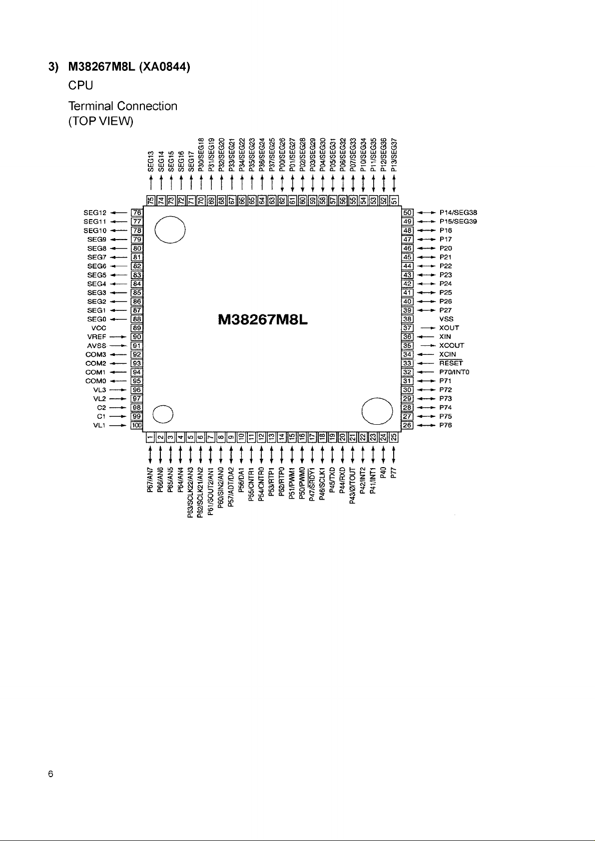
3) M38267M8L (XA0844)
CPU
Terminal Connection
(TOP VIEW)
6
Page 7
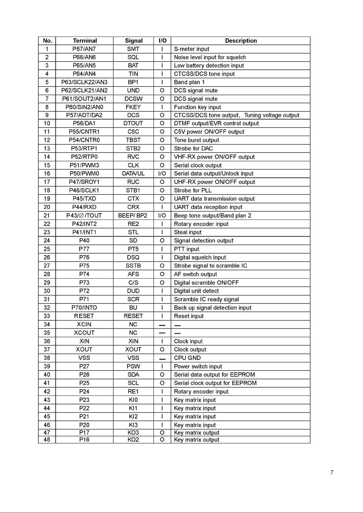
No. Terminal Signal I/O Description
1 P67/AN7 SMT I S-meter input
2 P66/AN6 SQL I Noise level input for squelch
3 P65/AN5 BAT I Low battery detection input
4 P64/AN4 TIN I CTCSS/DCS tone input
5 P63/SCLK22/AN3 BP1 I Band plan 1
6 P62/SCLK21/AN2 UND O DCS signal mute
7 P61/SOUT2/AN1 DCSW O DCS signal mute
8 P60/SIN2/AN0 FKEY I Function key input
9 P57/ADT/DA2 DCS O CTCSS/DCS tone output, Tuning voltage output
10 P56/DA1 DTOUT O DTMF output/EVR control output
11 P55/CNTR1 C5C O C5V power ON/OFF output
12 P54/CNTR0 TBST O Tone burst output
13 P53/RTP1 STB2 O Strobe for DAC
14 P52/RTP0 RVC O VHF-RX power ON/OFF output
15 P51/PWM3 CLK O Serial clock output
16 P50/PWM0 DATA/UL I/O Serial data output/Unlock input
17 P47/SROY1 RUC O UHF-RX power ON/OFF output
18 P46/SCLK1 STB1 O Strobe for PLL
19 P45/TXD CTX O UART data transmission output
20 P44/RXD CRX I UART data reception input
21 P43/0 /TOUT BEEP/ BP2 I/O Beep tone output/Band plan 2
22 P42/INT2 RE2 I Rotary encoder input
23 P41/INT1 STL I Steal input
24 P40 SD O Signal detection output
25 P77 PT5 I PTT input
26 P76 DSQ I Digital squelch input
27 P75 SSTB O Strobe signal to scramble IC
28 P74 AFS O AF switch output
29 P73 C/S O Digital scramble ON/OFF
30 P72 DUD I Digital unit detect
31 P71 SCR I Scramble IC ready signal
32 P70/INTO BU I Back up signal detection input
33 RESET RESET I Reset input
34 XCIN NC — —
35 XCOUT NC — —
36 XIN XIN I Clock input
37 XOUT XOUT O Clock output
38 VSS VSS
___
CPU GND
39 P27 PSW I Power switch input
40 P26 SDA O Serial data output for EEPROM
41 P25 SCL O Serial clock output for EEPROM
42 P24 RE1 I Rotary encoder input
43 P23 KI0 I Key matrix input
44 P22 KI1 I Key matrix input
45 P21 KI2 I Key matrix input
46 P20 KI3 I Key matrix input
47 P17 KO3 O Key matrix output
48 P16 KO2 O Key matrix output
7
Page 8
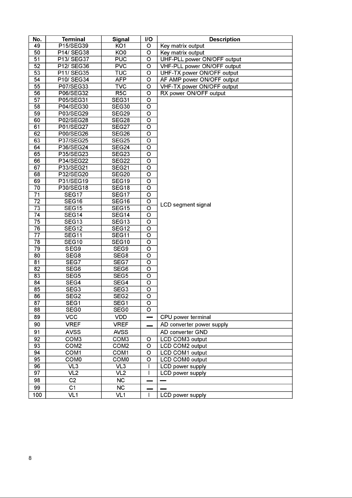
No. Terminal Signal I/O Description
49 P15/SEG39 KO1 O Key matrix output
50 P14/ SEG38 KO0 O Key matrix output
51 P13/ SEG37 PUC O UHF-PLL power ON/OFF output
52 P12/ SEG36 PVC O VHF-PLL power ON/OFF output
53 P11/ SEG35 TUC O UHF-TX power ON/OFF output
54 P10/ SEG34 AFP O AF AMP power ON/OFF output
55 P07/SEG33 TVC O VHF-TX power ON/OFF output
56 P06/SEG32 R5C O RX power ON/OFF output
57 P05/SEG31 SEG31 O
58 P04/SEG30 SEG30 O
59 P03/SEG29 SEG29 O
60 P02/SEG28 SEG28 O
61 P01/SEG27 SEG27 O
62 P00/SEG26 SEG26 O
63 P37/SEG25 SEG25 O
64 P36/SEG24 SEG24 O
65 P35/SEG23 SEG23 O
66 P34/SEG22 SEG22 O
67 P33/SEG21 SEG21 O
68 P32/SEG20 SEG20 O
69 P31/SEG19 SEG19 O
70 P30/SEG18 SEG18 O
71 SEG17 SEG17 O
72
73
SEG16
SEG15
SEG16
SEG15
O
LCD segment signal
O
74 SEG14 SEG14 O
75 SEG13 SEG13 O
76 SEG12 SEG12 O
77 SEG11 SEG11 O
78 SEG10 SEG10 O
79 SEG9 SEG9 O
80 SEG8 SEG8 O
81 SEG7 SEG7 O
82 SEG6 SEG6 O
83 SEG5 SEG5 O
84 SEG4 SEG4 O
85 SEG3 SEG3 O
86 SEG2 SEG2 O
87 SEG1 SEG1 O
88 SEG0 SEG0 0
89 VCC VDD
—
CPU power terminal
90 VREF VREF AD converter power supply
91 AVSS AVSS AD converter GND
92 COM3 COM3 O LCD COM3 output
93 COM2 COM2 O LCD COM2 output
94 COM1 COM1 O LCD COM1 output
95 COM0 COM0 O LCD COM0 output
96 VL3 VL3 I LCD power supply
97 VL2 VL2 I LCD power supply
98 C2 NC
99 C1 NC
100 VL1 VL1
— —
_
—
I
LCD power supply
8
Page 9
SEMICONDUCTOR DATA
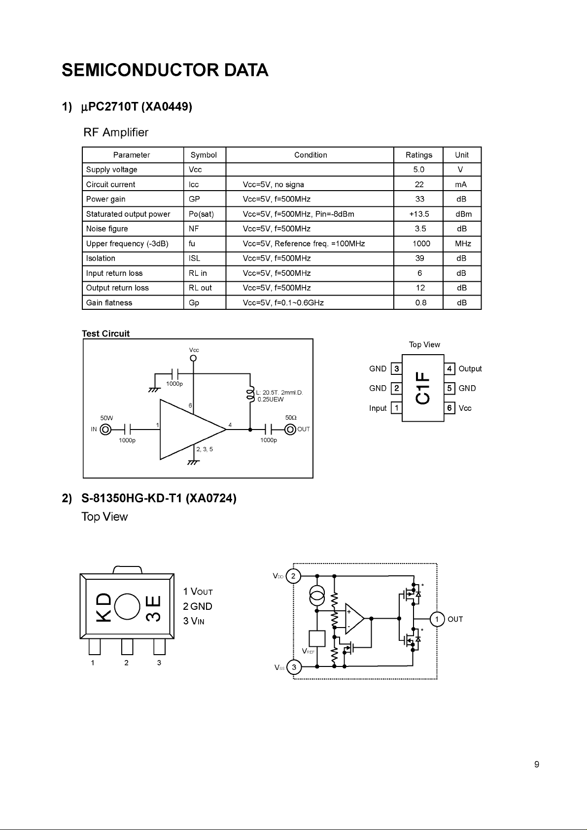
1) |j,PC2710T (XA0449)
RF Amplifier
Parameter Symbol Condition Ratings Unit
Supply voltage Vcc 5.0 V
Circuit current Icc Vcc=5V, no signa 22 mA
Power gain GP Vcc=5V, f=500MHz 33 dB
Staturated output power Po(sat) Vcc=5V, f=500MHz, Pin=-8dBm +13.5 dBm
Noise figure NF Vcc=5V, f=500MHz 3.5 dB
Upper frequency (-3dB) fu Vcc=5V, Reference freq. =100MHz 1000 MHz
Isolation ISL Vcc=5V, f=500MHz 39 dB
Input return loss RL in Vcc=5V, f=500MHz 6 dB
Output return loss RL out Vcc=5V, f=500MHz 12 dB
Gain flatness Gp Vcc=5V, f=0.1~0.6GHz 0.8 dB
Test Circuit
Vcc
Top View
2) S-81350HG-KD-T1 (XA0724)
Top View
GND
3
LL
GND 2 5
C)
1
Input
4
6
Output
GND
Vcc
9
Page 10
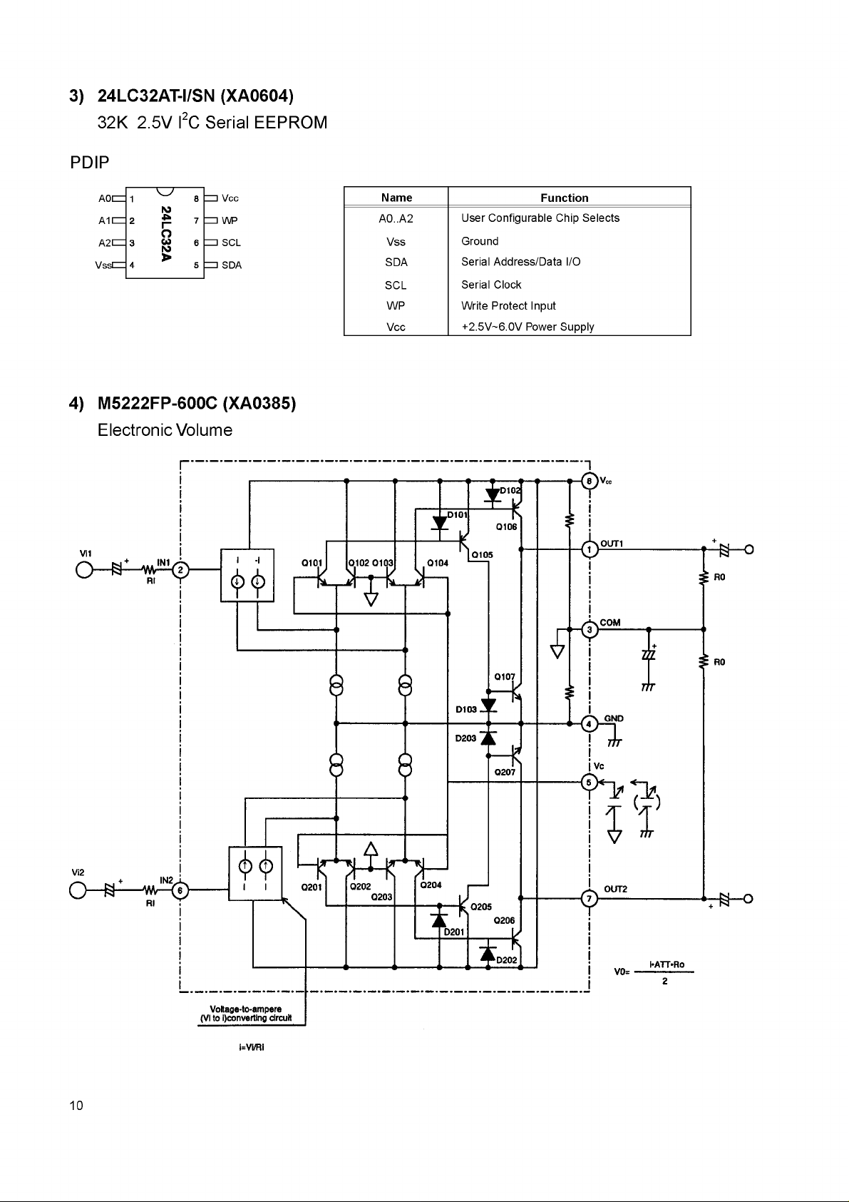
3) 24LC32AT-I/SN (XA0604)
32K 2.5V I2C Serial EEPROM
PDIP
A 0l=
A 1l= 2
A2 I= 3
Vssl=
1
M
4*
I-
o
w
IO
>
4
= l Vcc Name
8
7
= l WP
6 = l SCL
5
= l SDA
4) M5222FP-600C (XA0385)
Electronic Volume
A0..A2
Vss
SDA
SCL
WP Write Protect Input
Vcc
User Configurable Chip Selects
Ground
Serial Address/Data I/O
Serial Clock
+2.5V~6.0V Power Supply
Function
10
Page 11
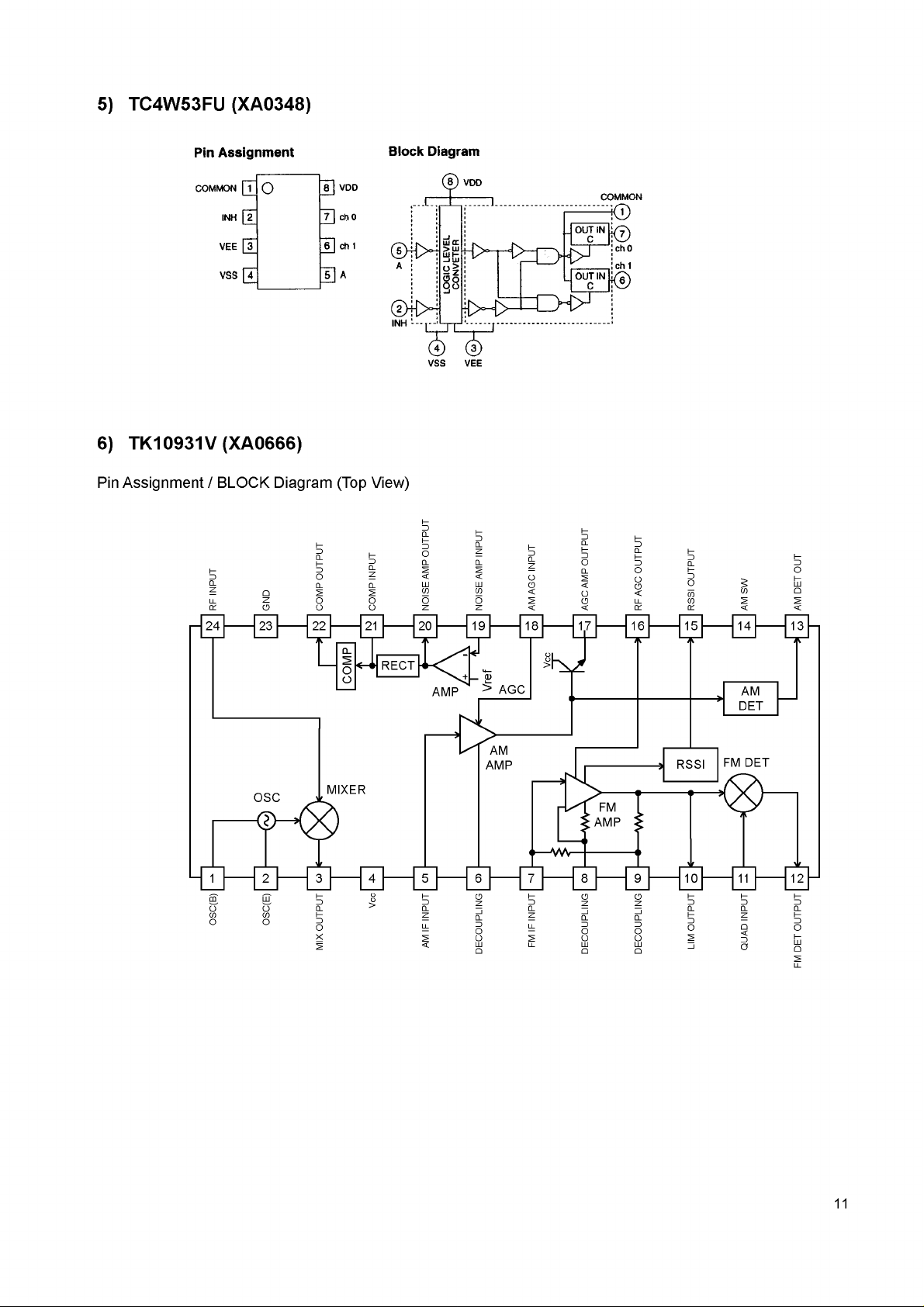
5) TC4W53FU (XA0348)
Block Diagram
8 ) VDD
...er
d>H>4
INH
6) TK10931V (XA0666)
Pin Assignment / BLOCK Diagram (Top View)
tU CE
>UI
S8
tO H >
VSS VEE
OUT IN i Q
OUT IN
m LU
ü ü
<0 <0
o o
ü O
z Z
CL CL
=) =)
o o
o o
LU LU
Q
O
Page 12
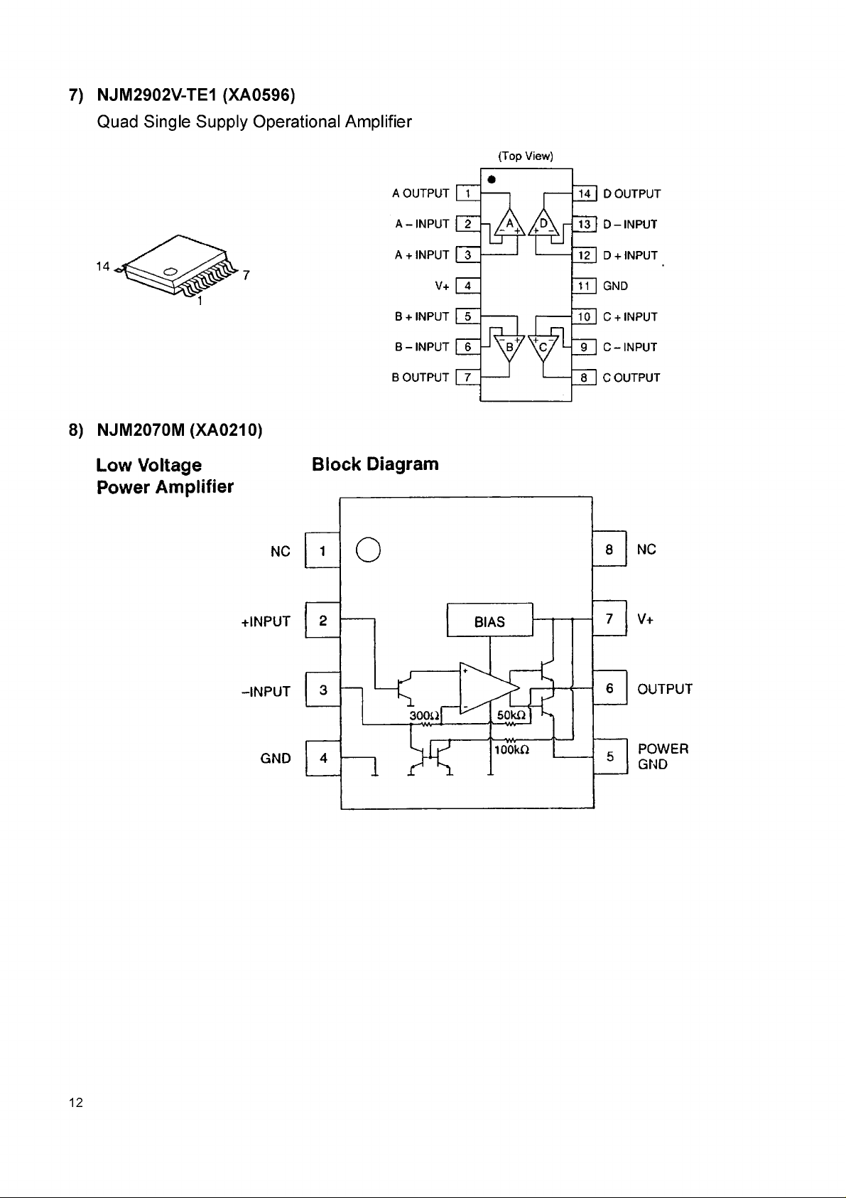
7) NJM2902V-TE1 (XA0596)
Quad Single Supply Operational Amplifier
8) NJM2070M (XA0210)
12
Page 13

9) |iPD3140GS-E1 (XA0312)
80 ~ 550MHz Dual PLL Synthesizer
Specifications
Operating frequency:
Consumption current:
Operationg voltage:
200 ~ 400MHz (Vin=-12 ~ 0dBm, pin 2 and 19 input)
80 ~ 550MHz (Vin=-8 ~ 0dBm, pin 2 and 19 input)
2.7 ~ 4.1mA (Vcc=1.8V while 1 channel is used)
4.3 ~ 6.6mA (Vcc=1.8V while both channels are used)
0 ~ 10uA (Vcc=1.8V in power save mode)
3.5 ~ 5.3mA (Vcc=5V while 1 channel is used)
5.6 ~ 8.6mA (Vcc=5V while both channels are used)
1.8 ~ 5.5V
Block Diagram
Vcc1 1
IN1 2
EN
CLK
DATA
TEST l~6
LOK 7
CP1
FL1
F01 10
4
Test selection circuit
Lock detection circuit
Charge
pump 1
_ n
Prescaler 1
Data
Interface
+ Latch
Filter 1
Phase Phase
comparator 1
comparator 2
Program
counter 1
Program
counter 2
Reference
counter 3
Prescaler 2
Crystal
oscillator
circuit
Charge
pump 2
Filter 2
20 GND1(A)
19 IN2
VCC2
18
XB
17
XI
16
15 XO
11 F02
Terminal Connection
Vcc1
[I
IN1 [ IF
EN 3
CLK 4
DATA 5
TEST 6
LOK 7
CP1
FL1 9
F01 10
GND1(A)
o
8
20
19 IN2
VCC2
18
17 XB
16 XI
15 XO
GND2(D)
14
CP2
13
12 FL2
11 F02
13
Page 14

10) BA4510FV-E2 (XA0537)
Dual Operational Amplifier
Vcc=± 2.5V Typ
High through rate: 5V/|iSec
Block Diagram
11) S-80845ALMP-EA9-T2 (XA0620)
Voltage Regulator
ounQ^
- m l T
i-w ilT
Vs
(Top View)
-------
W
A
"~T| QlTU
~a ] —im^
T ) -HM2
Vin= 18V
lo ut=100 m A
14
Page 15

12) MB88347LPFV-G-BND-EF (XA0599)
D/A converter for digital tuning
15
Page 16

13) Transistor, Diode, and LED Ontline Drawings
Top View
1SV214 TPH4
"" x b ö Í3 i
2SK882-GR-TE85L
......
MA132WA-TX
""XDQ321
RN11Q7 TE85L
UN911H TX
""Xu'Q092""
x'E0ö40'
s
R
TY
□
-----
XÏÏ0Î93
„C
XH
C
_EL
6 R
....
.......
......
Q
1SV279 (TPH3)
......
xDö364
......
2SK2975-T11-A
......
XE0038
.......
MA2SQ77-TX
""X D03Î9" "
A
s
RN1111 TE85L
XUO"^
X M
XP1111-TX
'''XÜ QÎ7T''
1SV307(TPH3)
""XÖQ326
p i.
: :
X
2SK3074
!!XEQÖ44!
n
W A
in n r
G S D
MA2S3Q4QQL
'""X 'D Q^
*
RN21Q7 TE85L
XÏÏ0Î92
„C
YH
XP1116-TX
" XÜQ"Í88""
......
....
.
.......
1SV311 TPL3
XDÖ344
BRPG1201W TR
XLGG28
.......
MA2S111-TX
"""xD"0323
XP15Q1-TX
"""XUÖT72"""
......
S3DG7
XD O^
SD
2SB766A-TX
"""XT0Ï7Q
Ü "
B
in n r
B C E
DA204U T106
""XDQÍ30
MA2S728-TX
""xD 'Ö3i5""
....
*
SML-31QMTT86
xL0ö36
2SC5Q66FT-Y(TE85L)
......
xt 0Y80
.........
C
M 2
DAN235E-TL
" " x Dq32q"" '
M
MA741WA TX
""xbQ 25i
......
M2P
D— n
U2FWJ44N(TE12R)
.......
xDo2"94""" "
2F
2SD2216R-TX
......
XT0135
........c........
ISS39Q TE61
■"XDÖ342""
RN731V TE-17
” IIIxDlQ257IIIII
UN9211 TX
" X"U0063""
.......
Y R
C
8 A
14) LCD Connection (EL0044)
OT - CN C O ^ lO ( Dr ^ OO O T T -T - T- T -T - T- T -T - T-T -C N C N C NC N C N C NCN C N C NCN C O C O
CDCDCDCDCDCDCDCDCDCDCDCDCDCDCDCDCDCDCDCDCDCDCDCDCDCDCDCDCDCDCDCD
LULULULULULULULULULULULULULULULULULULULULULULULULULULULULULULULU
cocococococococococococococococococococococococococococococococo
□ s(C1)
□4(C2)
O T - M C O ^ m ( D N C O O ) 0 ^ - M t 0 ^ l O C D N C O O ) O T -
16
Page 17

EXPLODED VIEW
1) Front View
KZ0133(DJ-596)
17
Page 18

2) Rear View
ST0063
18
Page 19

PARTS LIST
MAIN Unit
Ref. No.
C1 CU3535 Chip C. GRM36B102K 50PT
C2 CU3535 Chip C. GRM36B102K 50PT
C3 CU3517 Chip C. GRM36CH330J50PT
C4 CU3531 Chip C. GRM 36B471K50PT
C5 CU3507 Chip C. GRM36CH060D50PT
C6 CU3535 Chip C. GRM36B102K 50PT
C7 CU3517 Chip C. GRM36CH330J50PT
C8 CU3535 Chip C. GRM36B102K 50PT
C10 CU3503 Chip C. GRM36CK020C50PT
C11 CU3516 Chip C. GRM36CH270J50PT
C12 CU0108 Chip C. LMK212BJ105KG
C13 CU3535 Chip C. GRM36B102K50PT
C14 CU3531 Chip C. G RM36B471K50PT
C15 CS0408 Chip Tantalum 6M CM 156M ATER
C16 CU3535 Chip C. GRM36B102K50PT
C18 CU3502 Chip C. GRM36CK010C50PT
C19 CU3531 Chip C. G RM36B471K50PT
C20 CU0108 Chip C. LMK212BJ105KG
C21 CU3531 Chip C. G RM36B471K50PT
C22 CU3531 Chip C. G RM36B471K50PT
C24 CU3535 Chip C. GRM36B102K50PT
C25 CU3014 Chip C. C1608CH1H180JT-AS
C26 CU3535 Chip C. GRM36B102K50PT
C28 CU3531 Chip C. G RM36B471K50PT
C29 CU3547 Chip C. GRM36B103K16PT
C30 CU3531 Chip C. G RM36B471K50PT
C31 CU3502 Chip C. GRM36CK010C50PT
C32
C33 CU3502 Chip C. GRM36CK010C50PT
C34
C37 CU3502 Chip C. GRM36CK010C50PT
C38
C39 CU3531 Chip C. G RM36B471K50PT
C40
C42 CU3535 Chip C. GRM36B102K50PT
C43
C44 CU3515 Chip C. GRM36CH220J50PT
C45
C46 CU3535 Chip C. GRM36B102K50PT
C47
C48 CU3512 Chip C. GRM36CH120J50PT
C49
C50 CU3502 Chip C. GRM36CK010C50PT
Parts No.
FM0194 RADIATIVE PLATE
FG0291
TL0022 REFLECTIVE SHEET 195
TZ0049
DG0035 LCD LIGHT
FM0176
RD0108 J1/6Z
ST0063 LCD HOLDER DJ195
UP0429 PC Board XH791INTEGRATED
TS0148 VC O Sealed DJP85
TS0142 VCO Case XH 655
CU3535
CU3512
CU3531
CU3519
CU3535
CS0408 Chip Tantalum
CU3111
CU3519
Description Part Name Ver.
LCD RUBBER CONNECT.
SILICON D UMPER
PLUS TERMINAL DJ195
Chip C. GRM36B102K 50PT
Chip C.
Chip C. GRM36B471K 50PT
Chip C.
Chip C. GRM36B102K 50PT
Chip C.
Chip C.
GRM36CH120J50PT
GRM36CH470J50PT
6MCM 156MATER
C1608JB1C104KT-N
GRM36CH470J50PT
Ref. No. Parts No. Description Part Name Ver.
C52
CU3531
C53 CU3547 Chip C. GR M36B103K16PT
C54
CU3535
C55 CS0398 Chip Tantalum TM CP0J225MTR
C56
CU3531
C57 CU3531 Chip C. GR M36B471K50PT
C59 CS0403 Chip Tantalum TM CP1D 224MTR
C60 CU3516 Chip C. GRM36CH270J50PT
C61 CU3526 Chip C. GRM36CH181J25PT
C62 CU3531 Chip C. GR M36B471K50PT
C63 CU3531 Chip C. GR M36B471K50PT
C64 CU3547 Chip C. GR M36B103K16PT
C65 CU3531 Chip C. GR M36B471K50PT
C66 CU3111 Chip C. C1608JB1C104KT-N
C67 CS0403 Chip Tantalum TM CP1D 224MTR
C68 CU3531 Chip C. GR M36B471K50PT
C69 CU3531 Chip C. GR M36B471K50PT
C70 CU0108 Chip C. LMK212BJ105KG
C71 CU3511 Chip C. GRM36CH100D50PT
C72 CU3531 Chip C. GR M36B471K50PT
C73 CS0398 Chip Tantalum TM CP0J225MTR
C74 CU3516 Chip C. GRM36CH270J50PT
C75 CU3512 Chip C. GRM36CH120J50PT
C76 CU3531 Chip C. GR M36B471K50PT
C77 CU3510 Chip C. GRM36CH090D50PT
C78 CU0108 Chip C. LMK212BJ105KG
C79 CU3514 Chip C. GRM36CH180J50PT
C80 CU3501 Chip C. GRM36CK0R5C50PT
C81 CU3535 Chip C. GR M36B102K50PT
C82 CU3502 Chip C. GRM36CK010C50PT
C83 CU3535 Chip C. GR M36B102K50PT
C84 CU3535 Chip C. GR M36B102K50PT
C85 CU3535 Chip C. GR M36B102K50PT
C86
CU3510
C87 CU3506 Chip C. GRM36CH050C50PT
C88
CU3535
C89 CU3502 Chip C. GRM36CK010C50PT
C90
CU3502
C91 CU3535 Chip C. GR M36B102K50PT
C92
CU3535
C93 CU3529 Chip C. GR M36B331K50PT
C94
CU3535
C95 CU3511 Chip C. GRM36CH100D50PT
C96
CU3511
C97 CU3514 Chip C. GRM36CH180J50PT
C98
CU3535
C99 CU3501 Chip C. GRM36CK0R5C50PT
C100
CU3547
C101 CU3517 Chip C. GRM36CH330J50PT
C102
CU3519
C103 CU3517 Chip C. GRM36CH330J50PT
C104
CU3507
C105 CU3512 Chip C. GRM36CH120J50PT
C106
CU3516
Chip C. GRM36B471K 50PT
Chip C. GRM36B102K 50PT
Chip C. GRM36B 471K 50PT
Chip C.
Chip C. GRM36B 102K 50PT
Chip C.
Chip C. GRM36B 102K 50PT
Chip C. GRM36B 102K 50PT
Chip C.
Chip C. GRM36B 102K 50PT
Chip C. GRM36B 103K 16PT
Chip C.
Chip C.
Chip C.
GRM36CH090D50PT
GRM36CK010C50PT
GRM36CH100D50PT
GRM36CH470J50PT
GRM36CH060D50PT
GRM36CH270J50PT
19
Page 20

Ref. No. Parts No. Description Part Name Ver.
C107
CU3519
Chip C.
GRM36CH470J50PT
C108 CU3512 Chip C. GRM36CH120J50PT
C109 CU3547 Chip C. GRM 36B103K16PT
C110 CU3535 Chip C. GRM 36B102K50PT
C111 CU3547 Chip C. GRM36B 103K16PT
C112 CU3547 Chip C. GRM 36B103K16PT
C113 CU3515 Chip C. GRM36CH220J50PT
C114 CU3535 Chip C. GRM 36B102K50PT
C115 CU3531 Chip C. GRM 36B471K50PT
C116 CU3509 Chip C. GRM36CH080D50PT
C118 CU3503 Chip C. GRM36CK020C50PT
C119 CU3531 Chip C. GRM 36B471K50PT
C120 CU3515 Chip C. GRM36CH220J50PT
C121 CU3519 Chip C. GRM36CH470J50PT
C122 CU3547 Chip C. GRM 36B103K16PT
C123 CU3504 Chip C. GRM36CJ030C50PT
C124 CU3501 Chip C. GRM36CK0R5C50PT
C125 CU3501 Chip C. GRM36CK0R5C50PT
C126 CU3531 Chip C. GRM 36B471K50PT
C127 CU3515 Chip C. GRM36CH220J50PT
C128 CU3523 Chip C. GRM36CH101J50PT
C129 CU3535 Chip C. GRM 36B102K50PT
C130 CU3504 Chip C. GRM36CJ030C50PT
C131
CU3506
Chip C.
GRM36CH050C50PT
C132 CU3519 Chip C. GRM36CH470J50PT
C133
CU3506
Chip C.
GRM36CH050C50PT
C134 CU3507 Chip C. GRM36CH060D50PT
C135
CE0392 Electrolytic C.
6MV 47UW
C136 CU3547 Chip C. GRM36B103K16PT
C137
CU3504
Chip C.
GRM36CJ030C50PT
C138 CS0408 Chip Tantalum 6MC M156MATER
C139
CU3516
Chip C.
GRM36CH270J50PT
C140 CU3512 Chip C. GRM36CH120J50PT
C141
CU3516
Chip C.
GRM36CH270J50PT
C142 CU3535 Chip C. GRM36B102K50PT
C143
CU3535
Chip C.
GRM36B102K50PT
C144 CU3547 Chip C. GRM36B103K16PT
C145
CU3547
Chip C.
GRM36B103K16PT
C146 CU3515 Chip C. GRM36CH220J50PT
C147
CU3111
Chip C.
C1608JB1C104KT-N
C148 CU3111 Chip C. C1608JB1C104KT-N
C149
CU3111
Chip C.
C1608JB1C104KT-N
C150 CU0108 Chip C. LMK212BJ105KG
C151
CU3516
Chip C.
GRM36CH270J50PT
C154 CU3547 Chip C. GRM36B103K16PT
C155
CU3523
Chip C.
GRM36CH101J50PT
C156 CU3523 Chip C. GRM36CH101J50PT
C157 CU3111 Chip C. C1608JB1C104KT-N
C158 CU3547 Chip C. GRM36B103K16PT
C160 CU3535 Chip C. GRM36B102K50PT
C161 CU3535 Chip C. GRM36B102K50PT
C162 CU3535 Chip C. GRM36B102K50PT
C163 CU0108 Chip C. LMK212BJ105KG
C164 CE0392 Electrolytic C. 6MV4 7UW
C165 CU3535 Chip C. GRM 36B102K50PT
C166 CU3535 Chip C. GRM 36B102K50PT
C167 CE0373 Electrolytic C. 16MV 100UW
C169 CU3102 Chip C. C1608JB1C333KT-NS
C170 CU3535 Chip C. GRM 36B102K50PT
C171 CS0398 Chip Tantalum TMCP0J225M TR
C172 CU3535 Chip C. GRM 36B102K50PT
Ref. No. Parts No. Description Part Name Ver.
C173 CU3111 Chip C. C1608JB1C104KT-N
C174 CU3541 Chip C. GRM36B332K50PT
C175 CU3551 Chip C. GRM 36B223K16PT
C176 CU3551 Chip C. GRM 36B223K16PT
C177 CS0367 Chip Tantalum TMCM A0J106MTR
C178 CU3547 Chip C. GRM36B 103K16PT
C179 CS0408 Chip Tantalum 6MC M156MAT ER
C180 CU0108 Chip C. LMK212BJ105KG
C181 CU3538 Chip C. GRM36B 182K 50PT
C182 CS0403 Chip Tantalum TMC P1D224M TR
C183 CU0108 Chip C. LMK212BJ105KG
C184 CU3535 Chip C. GRM36B 102K50PT
C185 CU3550 Chip C. GRM36B 183K16PT
C186 CU3535 Chip C. GRM36B 102K50PT
C187 CE0315Z Electrolytic C. 16CV47BS
C188 CU3111 Chip C. C1608JB1C104KT-N
C189 CU3551 Chip C. GRM36B223K16PT
C190 CU3111 Chip C. C1608JB1C104KT-N
C191 CU3111 Chip C. C1608JB1C104KT-N
C192 CU3535 Chip C. GRM36B102K50PT
C193
CS0408 Chip Tantalum
6MCM 156MATER
C194 CE0308 Electrolytic C. 6.3CV 100BS
C195
CU0108
Chip C. LMK212BJ105KG
C196 CU3514 Chip C. GRM36CH180J50PT
C197
CU3513
Chip C.
GRM36CH150J50PT
C198 CU3544 Chip C. GRM36B562K25PT
C199
CU3540
Chip C.
GRM36B272K50PT
C201 CU3531 Chip C. GRM36B471K50PT
C202
CU3535
Chip C.
GRM36B102K50PT
C203 CU3547 Chip C. GRM36B103K16PT
C204
CS0408 Chip Tantalum 6MCM156MATER
C205 CU3546 Chip C. GRM36B822K16PT
C206
CU3047
Chip C.
C1608JB1H103KT-N
C207 CU3523 Chip C. GRM36CH101J50PT
C208
CU3523
Chip C.
GRM36CH101J50PT
C209 CU3111 Chip C. C1608JB1C104KT-N
C210
CU3539
Chip C.
GRM36B222K50PT
C211 CU3535 Chip C. GRM36B102K50PT
C212
CU3535
Chip C.
GRM36B102K50PT
C213 CS0403 Chip Tantalum TMCP1D224MTR
C214
CU3535
Chip C.
GRM36B102K50PT
C215 CU3535 Chip C. GRM36B102K50PT
C216
CU3111
Chip C.
C1608JB1C104KT-N
C218 CU3051 Chip C. C1608JB1E223KT-NS
C219
CU3111
Chip C.
C1608JB1C104KT-N
C220 CU0108 Chip C. LMK212BJ105KG
C221 CU3535 Chip C. GRM36B102K50PT
C222 CU3535 Chip C. GRM36B102K50PT
C223 CU3111 Chip C. C1608JB1C104KT-N
C224 CS0403 Chip Tantalum TMC P1D224M TR
C225 CU0108 Chip C. LMK212BJ105KG
C226 CU3535 Chip C. GRM36B102K50PT
C227 CU3539 Chip C. GRM36B222K50PT
C228 CU3111 Chip C. C1608JB1C104KT-N
C229 CU3521 Chip C. GRM36CH680J50PT
C23 CU3531 Chip C. GRM36B471K50PT
C230 CU3535 Chip C. GRM36B102K50PT
C231 CU3535 Chip C. GRM36B102K50PT
C232 CU3547 Chip C. GRM36B103K16PT
C233 CU3111 Chip C. C1608JB1C104KT-N
C234 CU0108 Chip C. LMK212BJ105KG
20
Page 21

Ref. No. Parts No. Description Part Name Ver.
C235
CS0408 Chip Tantalum 6MCM156MATER
C236 CU3018 Chip C. C1608CH1H390JT-AS
C237 CU3512 Chip C. GRM36CH120J50PT
C238 CU3515 Chip C. GRM36CH220J50PT
C239 CS0408 Chip Tantalum 6MC M156MATER
C241 CU3535 Chip C. GRM36B102K50PT
CN2 UE0369 Connector AXN49301616
D1 XD0326 Chip Diode 1SV307(TPH 3)
D2 XD0251 Chip Diode M A741WA TX
D3 XD0326 Chip Diode 1SV307(TPH 3)
D4 XD0326 Chip Diode 1SV307(TPH 3)
D5 XD0323 Chip Diode M A2S111-TX
D6 XD0343 Chip Diode M A2S304001AR
D7 XD0257 Chip Diode RN 731V TE-17
D9 XD0343 Chip Diode M A2S304001AR
D10 XD0251 Chip Diode MA741W A TX
D11 XD0364 Chip Diode 1SV279(TPH3)
D12 XD0319 Chip Diode MA2S077-TX
D13 XD0321 Chip Diode MA 132W A-TX
D14 XD0319 Chip Diode MA2S077-TX
D15 XD0131 Chip Diode 1SV214 TPH4
D16 XD0364 Chip Diode 1SV279(TPH3)
D17 XD0364 Chip Diode 1SV279(TPH3)
D18
XD0364
Chip Diode 1SV279(TPH3)
D19 XD0319 Chip Diode MA2S077-TX
D20
XD0343
Chip Diode MA2S304001A R
D21 XD0343 Chip Diode MA2S304001AR
D22
XD0343
Chip Diode MA2S304001A R
D23 XD0319 Chip Diode MA2S077-TX
D24
XD0343
Chip Diode MA2S304001AR
D25 XD0344 Chip Diode 1SV311 (TPL3)
D26
XD0344
Chip Diode 1SV311 (TPL3)
D27 XD0344 Chip Diode 1SV311 (TPL3)
D28
XD0319
Chip Diode MA 2S077-TX
D29 XD0342 Chip Diode 1S S390TE 61
D30
XD0344
Chip Diode 1SV311 (TPL3)
D31 XD0320 Chip Diode DAN235E-TL
D32
XD0320
Chip Diode DAN235E-TL
D33 XD0261 Chip Diode S3DG7
D35
XD0130
Chip Diode DA204U T106
D36 XD0315 Chip Diode MA2S728-TX
D37
XD0321
Chip Diode MA 132W A-TX
D38 XL0036 Chip LED SML-310MTT86
D39
XL0036
Chip LED SM L-310M TT86
D40 XL0036 Chip LED SML-310MTT86
D41
XL0036
Chip LED SM L-310M TT86
D42 XL0036 Chip LED SML-310MTT86
D43 XL0036 Chip LED SML-310MTT86
D44 XL0028 Chip LED B RPG1201W TR
D45 XD0323 Chip Diode MA2S111-TX
D46 XD0294 Chip Diode U2FWJ44N(TE12R)
D47 XD0323 Chip Diode MA2S111-TX
D48 XD0326 Chip Diode 1SV307(TPH3)
FL1 XC0053 Duplex Filter GDPX150/350A301
FL2 XC0079 Ceramic Filter ALFCM450E
FL3 XC0080 Ceramic Filter ALFCM450G
IC1 XA0449 IC UPC2710T-E3
IC2 XA0312 IC UPD3140G S-E1
IC3 XA0724 IC S81350HG-KD-T1
IC4 XA0599 IC MB88347LPFV-G-BND-EF
IC5 XA0666 IC TK10931VTL
Ref. No. Parts No. Description Part Name Ver.
IC6 XA0844 IC M38267M8L275GP
IC7 XA0604 IC 24LC32AT-I/SN
IC8 XA0596 IC NJM2902V-TE1
IC9 XA0210 IC NJM2070M T1
IC10 XA0385 IC M5222FP-600C
IC11 XA0620 IC S-80845ALMP-EA9-T2
IC13 XA0348 IC TC4W 53FU(TE12)
IC14 XA0537 IC BA4510FV-E2
IC15 XA0348 IC TC4W 53FU(TE12)
JK1 UJ0046 Jack MJ82-1
JK2 UJ0019 Jack HSJ1493-01-010
JK3 UJ0022 Jack HSJ1102-01-540
L1 QS35167 Coil 0.35-1.6-7T-L
L2 QC0547 Chip Inductor LK1608 R47K-T
L3 QS35165 Coil 0.35-1.60-5T-L
L4 QS2519A Coil 0.25-1.90-10T-L
L5 QB0045 Chip Inductor EXCCL3225U1
L6 QB0045 Chip Inductor EXCCL3225U1
L7 QC0600 Chip Inductor LQW1608AR22J00
L8 QC0533 Chip Inductor LQN21A39N J04
L9
QC0507 Chip Inductor
LK16081R0K-T
L10 QC0288 Chip Inductor NL252018T-1R0JA
L11
QC0538 Chip Inductor
LQN21AR10J04
L12 QS30093 Chip Inductor 0.30-0.90-3T -L
L13
QC0523 Chip Inductor
LQN21A3N3D04
L15 QC0538 Chip Inductor LQ N21AR 10J04
L16 QC0535 Chip Inductor LQ N21A56NJ04
L17 QC0616 Chip Inductor LL1608-FS12NJ
L18 QS40142 Coil 0.40-1.40-2T-L
L19 QC0507 Chip Inductor LK16081R0K-T
L20 QC0532 Chip Inductor LQ N21A33NJ04
L21 QC0507 Chip Inductor LK16081R0K-T
L22 QC0584 Chip Inductor LQW1608A10NJ00
L23 QC0595 Chip Inductor LQW1608A82NJ00
L24 QC0595 Chip Inductor LQW1608A82NJ00
L25 QC0595 Chip Inductor LQW1608A82NJ00
L26 QC0591 Chip Inductor LQW1608A39NJ00
L27 QC0590 Chip Inductor LQW1608A33NJ00
L28 QC0595 Chip Inductor LQW1608A82NJ00
L29 QC0506 Chip Inductor LK1608R56K-T
L30 QC0508 Chip Inductor LK16082R2K-T
L31 QC0506 Chip Inductor LK1608R56K-T
L32 QC0650 Chip Inductor LL1005FH10NJ
L33
QC0586 Chip Inductor LQW1608A15NJ00
L34 QC0586 Chip Inductor LQW1608A15NJ00
L35
QC0529 Chip Inductor
LQN21A18NJ04
L36 QC0587 Chip Inductor LQW1608A18NJ000
L37
QC0585 Chip Inductor LQW1608A12NJ00
L38 QC0592 Chip Inductor LQW1608A47NJ00
L39
QC0600 Chip Inductor LQW1608AR22J00
LCD1 EL0044 LCD HT-3404
MIC1
EY0017
XT0180 Chip Transistor 2SC5066FT-Y (TE85L)
Q1
Q2
XU0171 Chip Transistor
MIC O B-27P44
XP1111-T X
Q3 XT0135 Chip Transistor 2S D2216R -TX
Q4
XT0180 Chip Transistor 2SC5066FT-Y (TE85L)
Q5 XE0038 FET 2SK 2975-T11-A
Q6
XE0044
XT0180 Chip Transistor 2SC5066FT-Y (TE85L)
Q7
Q8
XT0180 Chip Transistor 2SC5066FT-Y (TE85L)
XU0063 Chip Transistor UN9211 TX
Q9
FET 2S K3074
21
Page 22

Ref. No. Parts No. Description Part Name Ver.
Q10 XU0172 Chip Transistor XP1501-T X
Q11 XU0172 Chip Transistor XP1 501-T X
Q12 XT0180 Chip Transistor 2SC5066FT-Y (TE85L)
Q13 XU0172 Chip Transistor XP1501-T X
Q14 XU0063 Chip Transistor UN9211 TX
Q15 XT0180 Chip Transistor 2SC5066FT-Y (TE85L)
Q16 XT0180 Chip Transistor 2SC5066FT-Y (TE85L)
Q17 XE0040 FET 2SK 882-GR-TE 85L
Q18 XT0180 Chip Transistor 2SC5066FT-Y (TE85L)
Q19 XT0180 Chip Transistor 2SC5066FT-Y (TE85L)
Q20 XT0180 Chip Transistor 2SC5066FT-Y (TE85L)
Q21 XT0135 Chip Transistor 2S D2216R -T X
Q22
XU0193 Chip Transistor
RN1107 TE85L
Q23 XU0193 Chip Transistor RN 1107 TE85L
Q24
XU0197 Chip Transistor
RN1111 (TE85L)
Q25 XT0170 Chip Transistor 2SB 766A-TX
Q26
XT0170 Chip Transistor
2SB766A-TX
Q27 XT0170 Chip Transistor 2SB 766A-TX
Q28
XU0188 Chip Transistor
XP1116-T X
Q29 XU0172 Chip Transistor XP1501-TX
Q30
XU0171 Chip Transistor
XP1111-T X
Q31 XU0171 Chip Transistor XP 1111-TX
Q32
XU0092 Chip Transistor
XP1501-T X
Q33 XU0092 Chip Transistor UN911H-TX
Q34
XU0192 Chip Transistor
RN2107 TE85L
Q35 XU0092 Chip Transistor UN911H-TX
Q36
XU0193 Chip Transistor
RN1107 TE85L
Q37 XU0192 Chip Transistor RN 2107 TE85L
Q38
XT0135 Chip Transistor
2SD2216R-TX
Q39 XU0193 Chip Transistor RN 1107 TE85L
Q40
XU0193 Chip Transistor
RN1107 TE85L
Q41 XU0193 Chip Transistor RN 1107 TE85L
Q42
XU0092 Chip Transistor
UN911H-TX
Q43 XU0197 Chip Transistor RN1111 (TE85L)
Q44
XU0197 Chip Transistor
RN1111 (TE85L)
Q45 XU0197 Chip Transistor RN1111 (TE85L)
Q46
XU0197 Chip Transistor
RN1111 (TE85L)
Q47 XU0193 Chip Transistor RN 1107 TE85L
Q48 XU0092 Chip Transistor UN911H-TX
Q49 XT0135 Chip Transistor 2SD 2216R -TX
Q50 XU0063 Chip Transistor UN9211 TX
R1 RK3558 Chip R. ERJ2G EJ473X
R2 RK3526 Chip R. ERJ2G EJ101X
R3 RK3530 Chip R. ERJ2G EJ221X
R4 RK3532 Chip R. ERJ2G EJ331X
R5 RK3526 Chip R. ERJ2G EJ101X
R6 RK3546 Chip R. ERJ2G EJ472X
R7 RK3524 Chip R. ERJ2G EJ680X
R9 RK3554 Chip R. ERJ2G EJ223X
R10 RK3526 Chip R. ERJ2GEJ101X
R11 RK3562 Chip R. ERJ2GEJ104X
R12 RK3550 Chip R. ERJ2GEJ103X
R13 RK3522 Chip R. ERJ2GEJ470X
R14 RK3516 Chip R. ERJ2GEJ150X
R15 RK3546 Chip R. ERJ2GEJ472X
R16 RK3550 Chip R. ERJ2GEJ103X
R17 RK3546 Chip R. ERJ2GEJ472X
R18 RK3546 Chip R. ERJ2GEJ472X
R19 RK3550 Chip R. ERJ2GEJ103X
R20
R21
RK3518
RK3518
Chip R. ERJ2GEJ220X
Chip R. ERJ2GEJ220X
Ref. No. Parts No. Description Part Name Ver.
R22 RK3561 Chip R. ERJ2GEJ823X
R23 RK3544 Chip R. ERJ2GEJ332X
R24 RK3548 Chip R. ERJ2GEJ682X
R25 RK3546 Chip R. ERJ2GEJ472X
R26 RK3526 Chip R. ERJ2GEJ101X
R27 RK3536 Chip R. ERJ2GEJ681X
R28 RK3550 Chip R. ERJ2GEJ103X
R29 RK3558 Chip R. ERJ2GEJ473X
R30 RK3526 Chip R. ERJ2GEJ101X
R31 RK3554 Chip R. ERJ2GEJ223X
R33 RK3546 Chip R. ERJ2GEJ472X
R34 RK3542 Chip R. ERJ2GEJ222X
R35 RK3550 Chip R. ERJ2GEJ103X
R36 RK3553 Chip R. ERJ2GEJ183X
R37 RK3550 Chip R. ERJ2GEJ103X
R38
RK3562
Chip R. ERJ2GEJ104X
R39 RK3562 Chip R. ERJ2GEJ104X
R40
RK3550
Chip R. ERJ2GEJ103X
R41 RK3548 Chip R. ERJ2GEJ682X
R42
RK3547
Chip R. ERJ2GEJ562X
R43 RK3546 Chip R. ERJ2GEJ472X
R44
RK3546
Chip R. ERJ2GEJ472X
R45 RK3538 Chip R. ERJ2GEJ102X
R46
RK3574
Chip R. ERJ2GEJ105X
R47 RK3554 Chip R. ERJ2GEJ223X
R48
RK3546
Chip R. ERJ2GEJ472X
R49 RK3543 Chip R. ERJ2GEJ272X
R50
RK3534
Chip R. ERJ2GEJ471X
R51 RK3542 Chip R. ERJ2GEJ222X
R52
RK3526
Chip R. ERJ2GEJ101X
R53 RK3562 Chip R. ERJ2GEJ104X
R54
RK3574
Chip R. ERJ2GEJ105X
R55 RK3550 Chip R. ERJ2GEJ103X
R56
RK3547
Chip R. ERJ2GEJ562X
R57 RK3526 Chip R. ERJ2GEJ101X
R58
RK3532
Chip R. ERJ2GEJ331X
R59 RK3550 Chip R. ERJ2GEJ103X
R60
RK3534
Chip R. ERJ2GEJ471X
R61 RK3550 Chip R. ERJ2GEJ103X
R62
RK3566
Chip R. ERJ2GEJ224X
R63 RK3547 Chip R. ERJ2GEJ562X
R64 RK3522 Chip R. ERJ2GEJ470X
R65 RK3534 Chip R. ERJ2GEJ471X
R66 RK3566 Chip R. ERJ2GEJ224X
R67 RK3534 Chip R. ERJ2GEJ471X
R68 RK3542 Chip R. ERJ2GEJ222X
R69 RK3550 Chip R. ERJ2GEJ103X
R70 RK3542 Chip R. ERJ2GEJ222X
R71 RK3562 Chip R. ERJ2GEJ104X
R72 RK3522 Chip R. ERJ2GEJ470X
R73 RK3562 Chip R. ERJ2GEJ104X
R74 RK3544 Chip R. ERJ2GEJ332X
R75 RK3518 Chip R. ERJ2GEJ220X
R76 RK3574 Chip R. ERJ2GEJ105X
R77 RK3574 Chip R. ERJ2GEJ105X
R78 RK3574 Chip R. ERJ2GEJ105X
R79 RK3574 Chip R. ERJ2GEJ105X
R80 RK3526 Chip R. ERJ2GEJ101X
R81 RK3538 Chip R. ERJ2GEJ102X
R82 RK3538 Chip R. ERJ2GEJ102X
R83 RK3568 Chip R. ERJ2GEJ334X
22
Page 23

Ref. No. Parts No. Description Part Name Ver.
R84 RK3539 Chip R. ERJ2GEJ122X
R85
RK3539
Chip R. ERJ2GEJ122X
R86 RK3562 Chip R. ERJ2GEJ104X
R87
RK3526
Chip R. ERJ2GEJ101X
R88 RK3544 Chip R. ERJ2GEJ332X
R89
RK3028
Chip R. MCR03EZHJ151
R90 RK3542 Chip R. ERJ2GEJ222X
R91
RK3562
Chip R. ERJ2GEJ104X
R92 RK3558 Chip R. ERJ2GEJ473X
R93
RK3501
Chip R. ERJ2GE0R00X
R94 RK3550 Chip R. ERJ2GEJ103X
R95
RK3544
Chip R. ERJ2GEJ332X
R96 RK3550 Chip R. ERJ2GEJ103X
R97
RK3550
Chip R. ERJ2GEJ103X
R98 RK3574 Chip R. ERJ2GEJ105X
R99
RK3574
Chip R. ERJ2GEJ105X
R100 RK3574 Chip R. ER J2G EJ105X
R101
RK3550
Chip R. ERJ2GEJ103X
R102 RK3562 Chip R. ER J2G EJ104X
R103
RK3552
Chip R. ERJ2GEJ153X
R104 RK3550 Chip R. ER J2G EJ103X
R105 RK3574 Chip R. ER J2G EJ105X
R106 RK3562 Chip R. ER J2G EJ104X
R107 RK3550 Chip R. ER J2G EJ103X
R108 RK3538 Chip R. ER J2G EJ102X
R109 RK3554 Chip R. ER J2G EJ223X
R110 RK3554 Chip R. ER J2G EJ223X
R111 RK3554 Chip R. ERJ2G EJ223X
R112 RK3551 Chip R. ERJ2GEJ123X
R113 RK3539 Chip R. ER J2G EJ122X
R115 RK3062 Chip R. M CR03EZHJ104 E
R116 RK3550 Chip R. ER J2G EJ103X
R117 RK3058 Chip R. M CR03EZHJ473
R118 RK0002 Chip R. ERJ6G EYJ120V
R119 RK3567 Chip R. ER J2G EJ274X
R120 RK3558 Chip R. ER J2G EJ473X
R121 RK3566 Chip R. ERJ2G EJ224X
R122 RK3546 Chip R. ER J2G EJ472X
R123 RK3556 Chip R. ER J2G EJ333X
R124 RK3552 Chip R. ER J2G EJ153X
R125 RK3565 Chip R. ER J2G EJ184X
R126 RK3501 Chip R. ERJ2GE0R 00X
R127
RK3542
Chip R. ERJ2GEJ222X
R128 RK3558 Chip R. ER J2G EJ473X
R129
RK3558
Chip R. ERJ2GEJ473X
R130 RK3550 Chip R. ER J2G EJ103X
R131
RK3538
Chip R. ERJ2GEJ102X
R132 RK3538 Chip R. ER J2G EJ102X
R133
RK3538
Chip R. ERJ2GEJ102X
R134 RK3554 Chip R. ER J2G EJ223X
R135
RK3550
Chip R. ERJ2GEJ103X
R136 RK3562 Chip R. ER J2G EJ104X
R137
RK3563
Chip R. ERJ2GEJ124X
R138 RK3542 Chip R. ER J2G EJ222X
R139
RK3562
Chip R. ERJ2GEJ104X
R140 RK3550 Chip R. ER J2G EJ103X
R141
RK3552
Chip R. ERJ2GEJ153X
R142 RK3562 Chip R. ER J2G EJ104X
R143
RK3556
Chip R. ERJ2GEJ333X
R144 RK3547 Chip R. ER J2G EJ562X
R145
RK3562
Chip R. ERJ2GEJ104X
Ref. No. Parts No. Description Part Name Ver.
R146
RK3550
Chip R. ERJ2GEJ103X
R147 RK3538 Chip R. ERJ2G EJ102X
R148
RK3550
Chip R. ERJ2GEJ103X
R149 RK3548 Chip R. ERJ2G EJ682X
R150
RK3554
Chip R. ERJ2GEJ223X
R151 RK3561 Chip R. E RJ2GEJ823X
R153
RK3552
Chip R. ERJ2GEJ153X
R154 RK3562 Chip R. ERJ2G EJ104X
R155
RK3557
Chip R. ERJ2GEJ393X
R156 RK3522 Chip R. ERJ2G EJ470X
R157
RK3526
Chip R. ERJ2GEJ101X
R158 RK3562 Chip R. ERJ2G EJ104X
R159
RK3548
Chip R. ERJ2GEJ682X
R160 RK3542 Chip R. ERJ2G EJ222X
R161 RK3532 Chip R. ERJ2G EJ331X
R162 RK3558 Chip R. ERJ2G EJ473X
R163 RK3561 Chip R. ERJ2GEJ823X
R164 RK3522 Chip R. ERJ2G EJ470X
R165 RK3559 Chip R. ERJ2G EJ563X
R166 RK3574 Chip R. ERJ2G EJ105X
R167 RK3550 Chip R. ERJ2G EJ103X
R168 RK3550 Chip R. ERJ2G EJ103X
R169 RK3562 Chip R. ERJ2G EJ104X
R170 RK3563 Chip R. ERJ2G EJ124X
R171 RK3526 Chip R. ERJ2G EJ101X
R172 RK3546 Chip R. ERJ2G EJ472X
R173 RK3546 Chip R. ERJ2G EJ472X
R174 RK3546 Chip R. ERJ2G EJ472X
R175 RK3546 Chip R. ERJ2G EJ472X
R176 RK3559 Chip R. ERJ2G EJ563X
R177 RK3563 Chip R. ERJ2G EJ124X
R178 RK3552 Chip R. ERJ2G EJ153X
R179 RK3550 Chip R. ERJ2G EJ103X
R180 RK3566 Chip R. ERJ2G EJ224X
R181 RK3550 Chip R. ERJ2G EJ103X
R182
RK3574
Chip R. ERJ2GEJ105X
R183 RK3556 Chip R. ERJ2G EJ333X
R184
RK3550
Chip R. ERJ2GEJ103X
R185 RK3550 Chip R. ERJ2G EJ103X
R186
RK3514
Chip R. ERJ2GEJ100X
R187 RK3550 Chip R. ERJ2G EJ103X
R188
RK3572
Chip R. ERJ2GEJ684X
R189 RK3550 Chip R. ERJ2G EJ103X
R190
RK3560
Chip R. ERJ2GEJ683X
R191 RK3567 Chip R. ERJ2G EJ274X
R192
RK3550
Chip R. ERJ2GEJ103X
R193 RK3553 Chip R. ERJ2G EJ183X
R194
RK3550
Chip R. ERJ2GEJ103X
R195 RK3554 Chip R. ERJ2G EJ223X
R196
RK3550
Chip R. ERJ2GEJ103X
R197 RK1018 Chip R. ERJ8GEYJ101V
R198
RK3566
Chip R. ERJ2GEJ224X
R199 RK3554 Chip R. ERJ2G EJ223X
R202
RK3550
Chip R. ERJ2GEJ103X
R203 RK3558 Chip R. ERJ2G EJ473X
R204
RK3565
Chip R. ERJ2GEJ184X
R205 RK3501 Chip R. ERJ2GE0R00X
R206
RK3550
Chip R. ERJ2GEJ103X
R207 RK3562 Chip R. ERJ2G EJ104X
R208
RK3550
Chip R. ERJ2GEJ103X
R209 RK3501 Chip R. ERJ2GE0R00X
23
Page 24

Ref. No. Parts No. Description Part Name Ver.
R210 RK3562 Chip R. ER J2G EJ104X
R211 RK3558 Chip R. ERJ2G EJ473X
R212 RK3558 Chip R. ER J2G EJ473X
R213 RK3532 Chip R. ER J2G EJ331X
R214 RK3536 Chip R. ER J2G EJ681X
R215 RK3567 Chip R. ER J2G EJ274X
R216 RK3554 Chip R. ER J2G EJ223X
R217 RK3552 Chip R. ER J2G EJ153X
R218 RK3562 Chip R. ER J2G EJ104X
R219 RK3566 Chip R. ER J2G EJ224X
R220 RK3574 Chip R. ER J2G EJ105X
R221 RK3554 Chip R. ERJ2G EJ223X
R222
RK3569
R223 RK3536 Chip R. ER J2G EJ681X
R224
RK3536
R225 RK3536 Chip R. ER J2G EJ681X
R226
RK3562
R227 RK3569 Chip R. ER J2G EJ394X
R228
RK3556
R229 RK3552 Chip R. ER J2G EJ153X
R230
RK3534
R231 RK3562 Chip R. ERJ2G EJ104X
R232
RK3557
R233 RK3558 Chip R. ER J2G EJ473X
R234
RK3550
R235 RK3550 Chip R. ER J2G EJ103X
R236
RK3574
R237 RK3562 Chip R. ER J2G EJ104X
R238
RK3562
R239 RK3538 Chip R. ER J2G EJ102X
R240
RK3574
R241 RK3574 Chip R. ERJ2G EJ105X
R242
RK3574
R243 RK3574 Chip R. ER J2G EJ105X
R244 RK3554 Chip R. ER J2G EJ223X
R245 RK3562 Chip R. ER J2G EJ104X
R246 RK3538 Chip R. ER J2G EJ102X
R247 RK3526 Chip R. ER J2G EJ101X
R251 RK3534 Chip R. ERJ2G EJ471X
SW17 UU0030 Switch EVQPJ005Q
SW18
UU0030
TC1 CT0045 Trimmer SMD3-010C1
VR1 RH0144 Trimmer Pot. MVR22HXBRN223
VR2 RH0144 Trimmer Pot. MVR22HXBRN223
VR3 RH0144 Trimmer Pot. MVR22HXBRN223
VR4 RH0144 Trimmer Pot. MVR22HXBRN223
W3 MACLH2GG Wire #30AH1-025-H1
W4 MRCKH5AA Wire #28R02-55-02
X1 XQ0139 Crystal UM5 12.9MHZ
X2 XK0003 Discriminator CDBM 450C7
X3 XQ0131 Crystal CSA310 3.686400MHZ
XF1 XF0039 Crystal Filter DSF753SB D39115GQ1
Chip R. ERJ2GEJ394X
Chip R. ERJ2GEJ681X
Chip R. ERJ2GEJ104X
Chip R. ERJ2GEJ333X
Chip R. ERJ2GEJ471X
Chip R. ERJ2GEJ393X
Chip R. ERJ2GEJ103X
Chip R. ERJ2GEJ105X
Chip R. ERJ2GEJ104X
Chip R. ERJ2GEJ105X
Chip R. ERJ2GEJ105X
Switch EVQPJ005Q
Mechanical Parts
Ref. No. Parts No. Description Part Name Ver.
SS0097 CHASSIS DJ596
FG0290 KL6767-PTT DJ195
YX0024 LCD TAPE DJ195
UR0019 RH70N00E20 (RY-6320)
TW0020 W.PROOF A XH720
NK0068 DIAL KNOB DJ195
KZ0133 FRONTCASE DJ596
FM0187 REAR PANEL DJ196
FM0179 ANTENNA EARTH PLATE
FM0178 PIN DJ195
FG0304 KL3735-3 16KEY DJ196
FG0289 TERMINAL RUBBER 195
UE0029A ANT.CONNECT.DJ460
AN0012 RND N7X0.75 BR/B.ZN
AF0031 SC REW
AK0001Z
AF0029 XQ N2+C9FN
FG0274
FG0286 KL6766-JACK CAPDJ195
FF0029
AF0020Z 1P 2X3 NIC
ES0011BZ
DP0142 LCD PANEL
W1 MACL07AA Wire #30A 02-070-02
W2 MPCL07AA Wire #30P 02-070-02
Speaker 036M9014B
BT 3P 2X4 NIC
DC CAP
CLOTH 4.0X22
Packing Parts
Ref. No. Parts No. Description Part Name Ver.
EG0043
EW0019 Wall charger 120V EDC-93 T
EW0020
EA0098 ANTENN A
#G0862
PS0380 INSTRUCTION MANUAL
PH0009A
DS0466 SPEC .SH EET
PR0478 CE LABEL E
PK0086 CIRCUIT DIAGRAM
PR0452 FCC HOME USE LABEL T
PR0447 FCC LABEL T
HK0512 PACAGE
HU0178 INNER
HU0181 INNER A
HM0209 CAR TO N 10
HU0170 INNER 10
HP0006Z PROTECTIO N BAG
PR0514
NiMH-Battery EBP50N
Wall charger 230V EDC-94 E
BELT CLIP
WARRANT Y T
E-10*4 9 LABEL
24
Page 25

ADJUSTMENT
1) Required Test Equipment
The following items are required to adjust radio parameters.
1. Regulated Power supply
Supply voltage:
Current:
2. Digital Multimeter
Voltage range:
Current:
Input resistance:
3. Oscilloscope
Measurable frequency:
4. Audio Dummy Load
Impedance:
Dissipation:
Jack:
5 to14 VDC
3A or more
FS = Approx. 20V
10A or more
High impedance
Audio Frequency
8Q
1W or more
3.5mm0
5. SSG
Output frequency:
Output level:
Modulation:
6. Spectrum Analyzer
Measuring range:
7. Power meter
Measurable frequency:
Impedance:
Measuring range:
8. Audio Voltmeter
Measurable frequency:
Sensitivity:
9. Audio Generator
Output frequency:
Output impedance:
10.Distortion Meter/SINAD Meter
Measurable frequency:
Input level:
Distortion level:
500MHz or more
-20dB|j/0.1|iV to 120dB|i/1V
FM
Up to 2GHz or more
Up to 500MHz
50Q, unbalanced
0.1W to 10W
Up to 100kHz
1mV to 10V
67Hz to 10kHz
600Q, unbalanced
1kHz
Up to 40dB
1% to 100%
25
Page 26

11.Frequency Counter
Measurable frequency:
Measurable stability:
12.Linear Detector
Measurable frequency:
Characteristics:
CN:
Note
Standard modulation:
Reference sensitivity:
Specified audio output level: 200mW at 8Q
Standard audio output level: 50mW at 8Q
Use an RF cable (3D2W:1m) for test equipment.
Attach a fuse to the RF indicated by EMF.
All SSG outputs are indicated by EMF.
Supply voltage for the transceiver: 13.8VDC
1kHz ± 3.5kHz /DEV
12dB SINAD
Up to 500MHz
Approx. ± O.ippm
Up to 500MHz
Flat
6Q dB or more
26
Page 27

2) Entering and releasing the adjustment mode
The DJ-596 does not require a serviceperson to manipulate the components
on the printed-circuit board, except the trimmer when adjusting reference
frequency and deviation. Most of the adjustments for the transceiver are made
by using the keys on it while the unit is in the adjustment mode. Because the
adjustment mode temporarily uses the channels, frequency must be set on
each channel before adjustments can be made. For instructions on how to
program the channels, see the “DJ-596 INSTRUCTION MANUAL “ which
came with the product. In consideration of the radio environment, the fre
quency on each channel must be near the value (+/-1MHz) listed in the table
below. To enter the adjustment mode, set key lock and input 490217. Decimal
point at 100MHz and 10MHz appears in LCD. (To release the mode, same
manner to enter the adjustment mode.)
Channel frequency used in the adjustment mode
Memory
Channel
1 Reference frequency 445 435
2 UH F high-power 445 435
3 U H F low-power 445 435
4 VH F high-power 145 145
5 V H F low-power 145 145
6 V HF minimum frequency sensitivity 136 136
7 VH F m edium frequency sensitivity 145 145
8 VH F m aximum frequency sensitivity 173 173
9 UH F minimum frequency sensitivity 41 0 410
10 U HF medium frequency sensitivity 445 435
11 U HF maximum frequency sensitivity 490 490
12 V HF S-m eter (1) 145 145
13 V HF S-m eter (FULL) 145 145
14 U HF S-m eter (1) 445 435
15 U HF S-m eter (FULL) 445 435
16 V HF wide deviation 145 145
17 V HF narrow deviation 145 145
18 U HF wide deviation 445 435
19 U HF narrow deviation 445 435
Channel Function
Frequency (MHz)
T E
27
Page 28

Reference frequency adjustment
1. In the adjustment mode, select channel 1 by rotating the main tuning dial.
2. Press the ( PTT) key to start transmission.
3. Rotate TC1 on the main board until the value on the frequency counter
matches the one displayed on the LCD.
UHF high-power adjustment
1. In the adjustment mode, select channel 2 by rotating the main tuning dial.
2. Hold down the ( PTT) key to start transmission.
3. While watching the reading of the TX power meter, set the output power to
the value closest to 4.5W by rotating the main tuning dial.
4. When the ( PTT) key is released, the output power at that time will be
stored as the high power setting.
UHF low-power adjustment
1. In the adjustment mode, select channel 3 by rotating the main tuning dial.
2. Hold down the ( PTT) key to start transmission.
3. While watching the reading of the TX power meter, set the output power to
4. When the ( PTT) key is released, the output power at that time will be
VHF high-power adjustment
1. In the adjustment mode, select channel 4 by rotating the main tuning dial.
2. Hold down the ( PTT) key to start transmission.
3. While watching the reading of the TX power meter, set the output power to
4. When the ( PTT) key is released, the output power at that time will be
VHF low-power
1. In the adjustment mode, select channel 5 by rotating the main tuning dial.
2. Hold down the ( PTT) key to start transmission.
3. While watching the reading of the TX power meter, set the output power to
the value closest to 0.8W by rotating the main tuning dial.
stored as the low power setting.
the value closest to 4.5W by rotating the main tuning dial.
stored as the high power setting.
the value closest to 0.8W by rotating the main tuning dial.
28
4. When the ( PTT) key is released, the output power at that time will be
stored as the low power setting.
Page 29

VHF minimum frequency sensitivity adjustment
See “Note on adjusting the sensitivity” later in this section.
1. In the adjustment mode, select channel 6 by rotating the main tuning dial.
2. Set the minimum frequency sensitivity rotating the main tuning dial, while F
appears after the (FUNC) key is pressed.
VHF medium frequency sensitivity adjustment
See “Note on adjusting the sensitivity” later in this section.
1. In the adjustment mode, select channel 7 by rotating the main tuning dial.
2. Set the medium frequency sensitivity rotating the main tuning dial, while F
appears after the (FUNC) key is pressed.
VHF maximum frequency sensitivity adjustment
See “Note on adjusting the sensitivity” later in this section.
1. In the adjustment mode, select channel 8 by rotating the main tuning dial.
2. Set the maximum frequency sensitivity rotating the main tuning dial, while F
appears after the (FUNC) key is pressed.
UHF minimum frequency sensitivity adjustment
See “Note on adjusting the sensitivity” later in this section.
1. In the adjustment mode, select channel 9 by rotating the main tuning dial.
2. Set the minimum frequency sensitivity rotating the main tuning dial, while F
appears after the (FUNC) key is pressed.
UHF medium frequency sensitivity adjustment
See “Note on adjusting the sensitivity” later in this section.
1. In the adjustment mode, select channel 10 by rotating the main tuning dial.
2. Set the medium frequency sensitivity rotating the main tuning dial, while F
appears after the (FUNC) key is pressed.
UHF maximum frequency sensitivity adjustment
See “Note on adjusting the sensitivity” later in this section.
1. In the adjustment mode, select channel 11 by rotating the main tuning dial.
2. Set the maximum frequency sensitivity rotating the main tuning dial, while F
appears after the (FUNC) key is pressed.
VHF S-meter (1) adjustment
1. In the adjustment mode, select channel 12 by rotating the main tuning dial.
The S-meter will show a single circle ( § )
2. Enter “0” dB^(EMF) with the transceiver tester (SSG).
3. Press the (FUNC) key The transceiver beeps indicating the new setting has
been stored successfully.
29
Page 30

VHF S-meter (FULL) adjustment
1. In the adjustment mode, select channel 13 by rotating the main tuning dial.
The S-meter will show all circles
2. Enter “+20” dB^ (EMF) with the transceiver tester (SSG).
3. Press the (FUNC) key. The transceiver beeps indicating the new setting has
been stored successfully.
UHF S-meter (1) adjustment
1. In the adjustment mode, select channel 14 by rotating the main tuning dial.
The S-meter will show a single circle ( § )
2. Enter “0” dB^ (EMF) with the transceiver tester (SSG).
3. Press the (FUNC) key . The transceiver beeps indicating the new setting
has been stored successfully.
UHF S-meter (FULL) adjustment
1. In the adjustment mode, select channel 15 by rotating the main tuning dial.
The S-meter will show all circles ( # # # # # # )
2. Enter “+20”dB^ (EMF) with the transceiver tester (SSG).
3. Press the (FUNC) key. The transceiver beeps indicating the new setting has
been stored successfully.
VHF wide deviation adjustment
1. In the adjustment mode, select channel 16 by rotating the main tuning dial.
2. Input a 50mVrms, 1kHz signal with your transceiver tester through the
external microphone jack.
3. With the tester, put the transceiver in the transmission mode.
4. Rotate the VR1 on the printed-circuit board of the transceiver until the
deviation is set to 4.5kHz.
VHF narrow deviation adjustment
1. In the adjustment mode, select channel 17 by rotating the main tuning dial.
2. Input a 50mVrms, 1kHz signal with your transceiver tester through the
external microphone jack.
3. With the tester, put the transceiver in the transmission mode.
4. Rotate the VR2 on the printed-circuit board of the transceiver until the
deviation is set to 2.2kHz.
UHF wide deviation adjustment
1. In the adjustment mode, select channel 18 by rotating the main tuning dial.
2. Input a 50mVrms, 1kHz signal with your transceiver tester through the
external microphone jack.
3. With the tester, put the transceiver in the transmission mode.
4. Rotate the VR3 on the printed-circuit board of the transceiver until the
deviation is set to 4.5kHz.
30
Page 31

UHF narrow deviation adjustment
1. In the adjustment mode, select channel 19 by rotating the main tuning dial.
2. Input a 50mVrms, 1kHz signal with your transceiver tester through the
external microphone jack.
3. With the tester, put the transceiver in the transmission mode.
4. Rotate the VR4 on the printed-circuit board of the transceiver until the
deviation is set to 2.2kHz.
Channel frequency used in the test mode
Memory
Channel
20 DTMF (1) 145 145
21 DTMF (D) 145 145
22 Tone 67Hz 145 145
23 Tone 88.5Hz 145 145
24 Tone 250.3Hz 145 145
25 DCS code 255 145 145
26 Tone Burst test 145 145
27 Digital mode deviation * 145 145
DTMF (1) test
DTMF (D) test
Channel Function
* : Required if EJ-43U is installed.
This function is only for checking the DTMF code, not adjusting it.
1. In the adjustment mode, select channel 20 by rotating the main tuning dial.
2. Press the ( PTT) key. DTMF code “1” is automatically sent and you will
hear the monitoring tone from the speaker.
3. Check the deviation with the transceiver tester, and make sure the deviation
level is within 2.1 to 3.7kHz range.
1. In the adjustment mode, select channel 21 by rotating the main tuning dial.
Frequency (MHz)
T E
Tone 67Hz test
2. Press the ( PTT) key. DTMF code “D” is automatically sent and you will
hear the monitoring tone from the speaker.
3. Check the deviation with the transceiver tester, and make sure the deviation
level is within 2.1 to 3.7kHz range.
This function is only for checking the tone encoder, not adjusting it.
1. In the adjustment mode, select channel 22 by rotating the main tuning dial.
2. Press the ( PTT) key. A 67Hz tone is automatically sent.
3. Check the deviation with the transceiver tester, and make sure the deviation
level is within 0.4 to 1.2kHz range.
31
Page 32

Tone 88.5Hz test
Tone 250.3Hz test
DCS code 255 test
Tone Burst test
1. In the adjustment mode, select channel 23 by rotating the main tuning dial.
2. Press the ( PTT) key. An 88.5Hz tone is automatically sent.
3. Check the deviation with the transceiver tester, and make sure the deviation
level is within 0.4 to 1.2kHz range.
1. In the adjustment mode, select channel 24 by rotating the main tuning dial.
2. Press the ( PTT) key. A 250.3Hz tone is automatically sent.
3. Check the deviation with the transceiver tester, and make sure the deviation
level is within 0.4 to 1.2kHz range.
This function is only for checking the DCS code encoder, not adjusting it.
1. In the adjustment mode, select channel 25 by rotating the main tuning dial.
2. Press the ( PTT) key. A 255 DCS code is automatically sent.
3. Check the deviation with the transceiver tester, and make sure the deviation
level is within 0.5 to 1.5kHz range.
This function is only for checking the tone burst, not adjusting it.
1. In the adjustment mode, select channel 26 by rotating the main tuning dial.
2. Press the ( PTT) key. A 1750Hz tone burst is automatically sent.
3. Check the deviation with the transceiver tester, and make sure the deviation
level is within 2.3 to 3.7kHz range.
Digital mode deviation test (Optional EJ-43U required)
This function is only for checking the digital mode deviation, not adjusting it.
1. In the adjustment mode, select channel 27 by rotating the main tuning dial.
2. Press the ( PTT) key. A digital code “000000” is automatically sent.
3. Check the deviation with the transceiver tester, and make sure the deviation
level is within 2.8 to 3.7kHz range.
32
Page 33

PC BOARD VIEW
MAIN SIDE A
33
Page 34

MAIN SIDE B
34
Page 35

SCHEMATIC DIAGRAM DJ-596
35
Page 36

BLOCK DIAGRAM DJ-596
36
Page 37

ALINCO, INC
Head Office : Shin-Dai Building 9th Floor
2-6, 1-Chome, Dojimahama, Kita-ku, Osaka 530-0004, Japan
Phone: +81-6-4797-2136 Fax: +81-6-4797-2157
E-mail:export@alinco.co.|p
Dealer/Distributor
V
_________________
Copyright 2001 Alinco, lnc. Osaka Japan
Printed in Japan
_______
PM0071
/
 Loading...