

Alinco DJ-580E, DJ-580T Service Manual
DJ-580T/E
Service Manual
• Specifications
• Circuit Description
• Semiconductor Data
• Exploded View....................................23 - 28
• PC Board View...................................29-38
• Parts List
• Adjustment..........................................53 - 58
• Block Diagram....................................59 - 60
• Circuit Diagram...................................61 - 67
........................................
................................4-14
..........................
.............................................39-52
2 -3
15-22
ALINCO ELECTRONICS INC
Specifications
I General
Channel Spacing:
Memory Channels:
Signal Type:
Antenna Impedance:
Microphone Impedance:
Speaker Impedance:
Power Supply Requirements:
Dimensions (Radio Only):
Weight:
DTMF:
Subaudible Tones:
U.S. Frequency Coverage
The frequency coverage listed as follows applies to DJ-580T.
VHF Band: 144.000 - 147.995MHz (TX)
UHF Band: 440.000 - 449.995MHz (TX)
5, 10, 12.5, 15, 20, 25 KHz steps
42 Channels (40 total combination of VHF and UHF)
1 VHF Call Channel
1 UHF Call Channel
F3E(FM)
50Q unbalanced
2kn unbalanced
8ft unbalanced
13.8 Volts DC (Rated 9 volts DC)
140(H) x 58(W) x 33(D) mm
Approximately 410g
16 Button Key Pad
Encode and Decode installed
130.000 - 173.995MHz (RX)
110.000 ~ 142.995MHz (RX) Only after Modification
420.000 - 479.995MHz (RX)
European Frequency Coverage
The frequency coverage listed as follows applies to DJ-580E.
VHF Band:
UHF Band:
144.000 ~ 145.995MHz (TX/RX)
430.000 - 439.995MHz (TX/RX)
Transmitter
Output Power:
Modulation System:
Max. Frequency Deviation:
Spurious Emission:
Tone Frequency:
Microphone:
Operating Mode:
Simplex:
Duplex:
CTCSS Encoder:
CTCSS Decoder:
Approximately 2Watts with Standard EBP-20N Battery
Approximately 5Watts with Optional EBP-22N Battery
Variable reactance FM
+/- 5 kHz
Less than 60dB below carrier
67.0 to 250.3Hz (38 selections)
DJ-580T (Subaudible Encoding Tone)
DJ-580E (1,750Hz Tone Burst)
Electret Condenser
5KHz steps minimum between 0 ~ 15.995MHz from receive frequency.
Built-in and included as standard for DJ-580T
Built-in and included as standard for DJ-580T
2
■ Receiver Specifications
Receiver System: Superheterodyne, Dual Conversion
Sensitivity: 12dB SINAD less than -15dB^iV
Intermediate Frequency: VHF — 1st IF 55.05MHz
2nd IF 455kHz
UHF — 1st IF 23.05MHz
2nd IF 455kHz
Audio Power Output: 250mW (at 10% T.H.D.)
Speaker Impedance: 8ft
Circuit Description
1. Receiver System
VHF and UHF receiver systems are the double superheterodyne. In VHF receiver system, the first IF is
55.05 MHz and the second IF is 455KHz. In UHF receiver systemjhe first IF is 23.05 MHz and the second
IF is 455KHZ.
1.1 Front End
VHF:
The signal from the antenna is passed through a
duplexer and an antenna switch, and then input to
the RF coil L418.
The signal from L418 is amplified by Q416 and led
to the band pass filter (L420, L421), and led to the
first mixer base of Q417.
1.2 First Mixer
VHF:
The signal (fo) is mixed with the first local oscillator
signal (fo+55.05MHz) from the PLL circuit by the
first-stage mixer Q417 and so is converted into the
first IF signal.
The unwanted frequency band of the first IF signal
is eliminated by the monolithic crystal filter (L423,
L424, XF402).
UHF:
The signal from the antenna is passed through a
duplexer and an antenna switch, and then input to
the RF coil L405.
The signal from L405 is amplified by Q404 and led
to the band pass filter (L406, L407), passed through
the band pass filter (L408, L409), and then led to
the first mixer base of Q406.
UHF:
The signal (fo) is mixed with the first local oscillator
signal (fo-23.05MHz) from the PLL circuit by the
first-stage mixer Q406 and so is converted into the
first IF signal.
The unwanted frequency band of the first IF signal
is eliminated by the monolithic crystal filter (XF401).
1.3 IF Amplifier
VHF:
The first IF signal is amplified by Q418 and Q107,
and input to pin 20 of IC102, where it is mixed with
the second local oscillator signal (54.595MHz) and
so is converted into the second IF signal (455KHz).
The second IF signal is output from pin4 of IC102,
and unwanted frequency band of the second IF
signal is eliminated by a ceramic filter (FL102), and
input to pin6 of IC102.
The resulting signal is then amplified by the second
IF limiting amplifier, and detected by quadrature
circuit, and the audio signal is output from pin11 of
IC102.
UHF:
The first IF signal is amplified by Q403 and Q101,
and input to pin 20 of IC101, where it is mixed with
the second local oscillator signal (22.595MHz) and
so is converted into the second IF signal (455KHz).
The second IF signal is output from pin4 of IC101,
and unwanted frequency band of the second IF
signal is eliminated by a ceramic filter (FL101), and
input to pin6 of IC101.
The resulting signal is then amplified by second IF
limiting amplifier, and detected by quadrature
circuit, and the audio signal is output from pin11 of
IC101.
4
1.4 Audio Circuit
VHF:
The signal from pin 11 of IC102 is filtered with
de-emphasis circuit (consists of R156, C153, R157,
C154), and led to the mute circuit Q109, passed
through the AF variable resister (VR102-B) and
amplified by the power amplifier IC106 to drive the
speaker.
1.5 Squelch Circuit
VHF:
The audio signal from pinil of IC102 is passed
through the squelch control variable resistor
(VR102-A) and input to pin13 of IC102. The audio
signal is amplified by IC102 and output to pin14.
The desired noise of the audio signal is eliminated
by the high pass filter consisting of C147 and R166,
and amplified by Q108. The resulting signal is recti
fied by D105 and then input to pin15 of JC102.
When the voltage of p»m5 is below 0.7V, SDV goes
to "Lo”. When the voltage of pin 15 is over 0.7V,
SDV goes to "Hi". The SDV signal is input to pin 14
of IC107.
UHF:
The signal from pin 11 of IC102 is filtered with
de-emphasis circuit (consists of R124, C119, R125,
C120), and led to the mute circuit Q103, passed
through the AF variable resister (VR101-B) and
amplified by the power amplifier IC106 to drive the
speaker.
UHF:
The audio signal from pin11 of IC101 is passed
through the squelch control variable resistor
(VR101-A) and input to pin13 of IC101. The audio
signal is amplified by IC101 and output to pin 14.
The desired noise of the audio signal is eliminated
by the high pass filter consisting of C115 and R115,
and amplified by Q102. The resulting signal is recti
fied by D101 and then input to pin15 of IC101.
When the voltage of pin15 is below 0.7V, SDU goes
to "Lo". When the voltage of pin 15 is over 0.7V,
SDU goes to "Hi". The SDU signal is input to pin15
of IC107.
1.6S-meter Circuit
VHF:
The DC voltage of pin12 of IC102 is passed
through VR104 and input to pin75 of IC107. The
DC voltage is digitized to control the LCD S-meter
display.
UHF:
The DC voltage of pin 12 of C101 is passed through
VR103 and input to pin74 of IC107. The DC volt
age is digitized to control the LCD S-meter display.
1.7 AM, AGC Circuit
VHF:
AM audio signal from pin12 of IC102 is amplified
by Q110, and supplied to pin 6 and pin7 of IC106.
The S-meter signal from pin12 of IC102 is supplied
to Q106. The gain of the second IF amplifier is con
trolled by the collector current of Q106, and the
input level of pin 20 of IC102 is stabilized.
1.8 Cross Band Repeater Circuit
When the transceiver receives the VHF or UHF signal in the cross band repeater mode: it will be retransmitted
from main band. The audio signal is passed through the cross band repeater switch Q105, and supplied to
microphone amplifier IC105.
5
2. Transmitter System
2.1 Microphone Amplifier
VHF/UHF:
The voice from the internal or external microphone is led to pre-emphasis circuit, and then input to the
microphone amplifier IC105, which consists of two operational amplifiers.
The output from the microphone amplifier is passed through variable resistors VR106 (VHF) and VR105
(UHF) for modulation adjustment to varicap diode of the VCO, controlling the VCO frequency.
2.2 Power amplifier
VHF:
The signal from VCO is amplified by a buffer ampli
fier Q420, and input to the power module pin1 of IC
402 . The amplified signal is output from pin5, and
then passed through the low-pass filter and the an
tenna switch circuit. The unwanted harmonics
frequency signal is eliminated by the low-pass filter
in the duplexer and input to the antenna.
UHF:
The signal from VCO is amplified by a buffer ampli
fier Q408, and input to the power module pin1 of IC
401. The amplified signal is output from pin5, and
then passed through the low-pass filter and the an
tenna switch circuit. The unwanted harmonics
frequency signal is eliminated by the low-pass filter
in the duplexer and input to the antenna.
2.3 Automatic Power Control Circuit
VHF:
The automatic power control(APC) circuit is used to
obtain a stable transmission power. This circuit
detects the transmission power by D409 in the low-
pass filter consisting of L425, C514, C515, and
C516. The detected DC voltage is supplied to APC
circuit consisting of Q411, Q412, Q413, and D410.
The detected voltage to G411 is passed through
Q412, Q413 and Q414, and then controls the
emitter current of Q420.
UHF:
The automatic power control(APC) circuit is used to
obtain a stable transmission power. This circuit
detects the transmission power by D408 in the low-
pass filter consisting of L403, C421, C422, and
C450. The detected DC voltage is supplied to APC
circuit consisting of Q411, Q412, Q413, and D410.
The detected voltage to Q411 is passed through
Q412, Q413 and Q414, and then controls the
collector voltage of Q408.
6
3. PLL Circuit
VHF:
Output frequency of PLL circuit is set by the serial
data from microprocessor IC107.
The data (strobe, clock, data) are consisted of 16
bits serial data. The VCO output frequency is
supplied to pin10 of IC404. The programmable
divider in IC404 divides the VCO output
frequency, and generates 5 or 6.25KHz.
PLL circuit generates TX frequency (fo) and RX
frequency (fo + 55.05MHz).
3.1 Reference Divider Circuit
VHF:
The channel step is determined by the reference
frequency.
6 channel steps (5, 10, 15, 12.5, 20, 25KHz) are
obtained when the reference oscillation frequency
(12.8MHz) is divided.
The reference frequency (5KHz) uses a channel
step of 5, 10, 15, 20 or 25KHz.
The reference frequency (6.25KHz) uses the chan
nel step of 12.5KHz. The frequencies multiplied by
the even numbers of 12.5KHz use the reference
frequency of 5KHz.
UHF:
Output frequency of PLL circuit is set by the serial
data from microprocessor IC107.
The data (strobe, clock, data) are consisted of 16
bits serial data. The VCO output frequency is
supplied to pin10 of IC403. The programmable
divider in IC403 divides the VCO output
frequency, and generates 5 or 6.25KHz.
PLL circuit generates TX frequency (fo) and RX
frequency (fo -23.05MHz).
UHF:
The channel step is determined by reference
frequency.
6 channel steps (5, 10, 15, 12.5, 20, 25KHz) are
obtained when reference oscillation frequency
(12.8MHz) is divided.
The reference frequency (5KHz) uses a channel
step of 5,10,15,20 or25KHz.
The reference frequency (6.25KHz) uses the chan
nel step of 12.5KHz. The frequencies multiplied by
the even numbers of 12.5KHZ use the reference
frequency of 5KHz.
3.2 Phase Comparison Circuit (P/C)
VHF:
A comparison frequency is obtained when the
VCO output is divided in IC404 (pulse swallow
system-based PLL IC).
3.3 PLL Loop Filter Circuit
VHF:
The pulse wave output of charge pump is con
verted to DC voltage by PLL loop filter circuit, and
supplied to D423, D424 of varicap diode in VCO
unit.
3.4 VCO Circuit
VHF:
The VCO tune voltage is applied to the varicaps
D423 and D424.
The frequency modulation is executed when the
audio signal voltage is supplied to the varicaps
D424 and D425.
UHF:
A comparison frequency is obtained when the
VCO output is divided in IC403 (pulse swallow
system-based PLL IC).
UHF:
The pulse wave output of charge pump is converted
to DC voltage by PLL loop filter circuit, and supplied
to D421, D422 of varicap diode in VCO unit.
UHF:
The VCO tune voltage is applied to the varicaps
D421 and D422.
The frequency modulation is executed when the
audio signal voltage is supplied to the varicap D418.
7
4. DTMF Circuit
4.1 Decoder
The detected signal from pin11 of IC101 and IC102 is passed through VHF/UHF selector consisting of Q142
and Q111, and input to the DTMF decoder pin8 of IC108. The VHF/UHF selector is controlled by BND from
pin42 of IC107. When the input signal is valid, the digital signal is output from pin1(D2), pin2(D1), pin15(D8)
and pin 16(D4) of IC108, and then input to pin48(DD2), pin47(DD1), pin50(DD8) and pin49(DD4) of IC107.
4.2 Encoder
The DTMF signal corresponding to the combination of the column and row is output from tone output pin 17
of IC3. When using the DTMF Keypad, IC107 pin 31 (IN 0), pin 32(IN 1), pin33(IN 2), pin 34(IN 3) and pin51(OTO),
pin 52(OT 1), pin53(OT2), pin54(OT3) go to high impedance.
There are pull-up register (ROW) and pull-down register (COL) inside IC3. When the keyboard is pressed,
ROW input and COL input are connected, and the input voltage goes to half level, then the DTMF is output.
When the DTMF encoder is controlled by IC107, one of INO, IN1, IN2 and IN3 goes to "High”, and one of OTO,
OT1, OT2 and OT3 goes to "Low”. The DTMF signal is output corresponding to the input data.
5. Tone Squelch Circuit
5.1 Decoder
VHF/UHF:
The second IF signal from pin 11 of IC101 and IC102, is passed through VHF/UHF selector consisting of Q142
and Q111, and input to the tone squelch decoder pin24 of IC701. The VHF/UHF selector is controlled by BND
from pin42 of IC107.
When the tone squelch decoder IC701 decodes the input tone signal frequency as the programmed frequency,
pin13 goes to "Low”. The signal is input to pin16(DET) of IC107, and the squelch goes off.
When the Tone squelch decoder IC701 does not decode the input tone signal frequency as the programmed
frequency, pin 13 goes to "High” The signal is input to pin16(DET) of IC107, and the squelch goes on.
5.2 Encoder
VHF:
The tone signal is output from pin16 of IC701, and
amplified at Q701, then output to the TO(MOV)
terminal.
UHF:
The tone signal is output from pin16 of IC701, and
amplified at Q701, then output to the TO(MOU)
terminal.
6.1750Hz Tone Burst Circuit
The 1750Hz Tone Burst signal is generated by IC107.
The signal is passed through the VR111, and supplied to MOV, MOU terminal.
&Tone Burst Circuit is built in DJ-580E only.
8
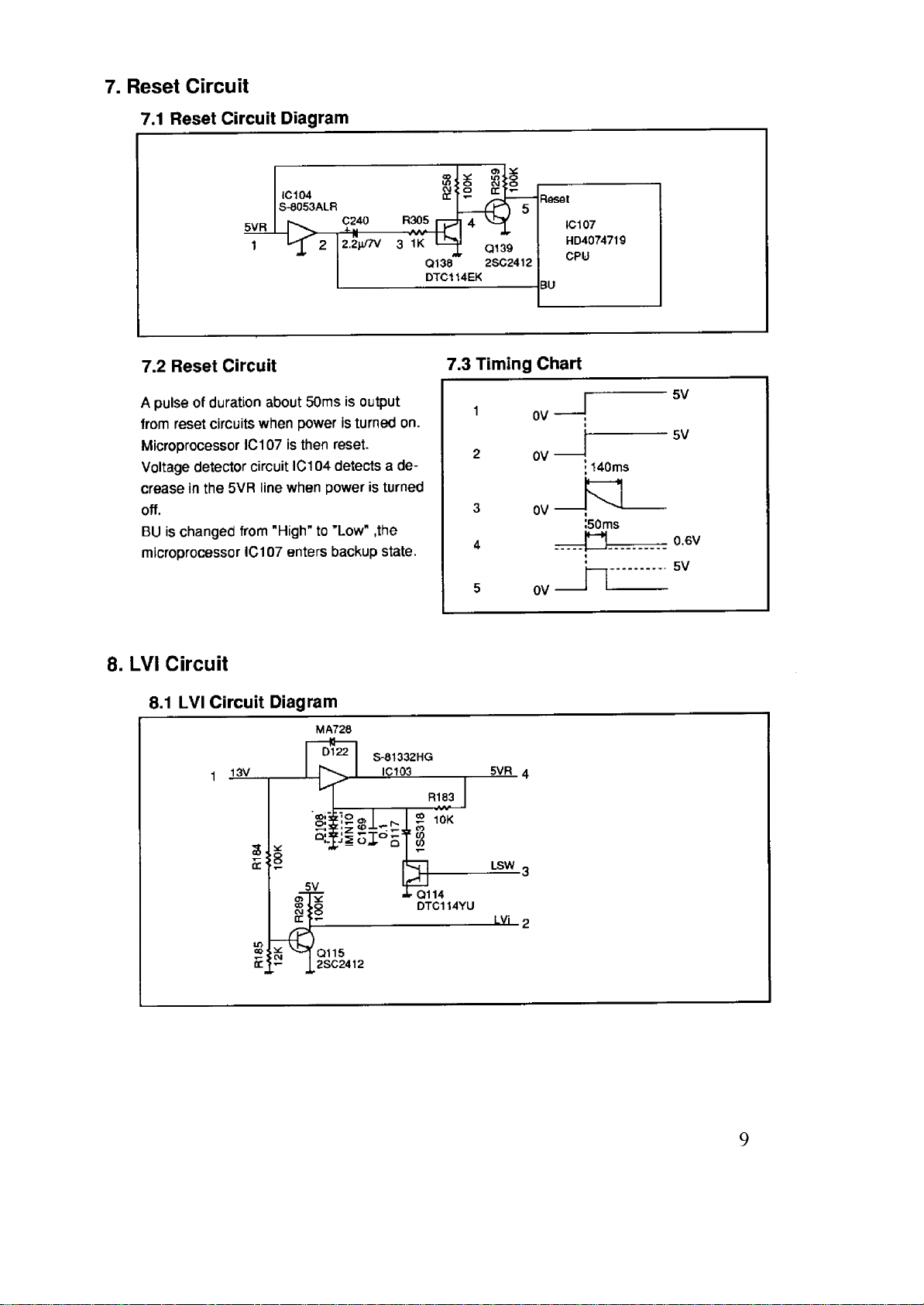
7. Reset Circuit
7.1 Reset Circuit Diagram
7.2 Reset Circuit
A pulse of duration about 50ms is output
from reset circuits when power is turned on.
Microprocessor IC107 is then reset.
Voltage detector circuit IC104 detects a de
crease in the 5VR line when power is turned
off.
BU is changed from "High" to ’Low" ,the
microprocessor IC107 enters backup state.
8. LVI Circuit
8.1 LVI Circuit Diagram
MA728
7.3 Timing Chart
9
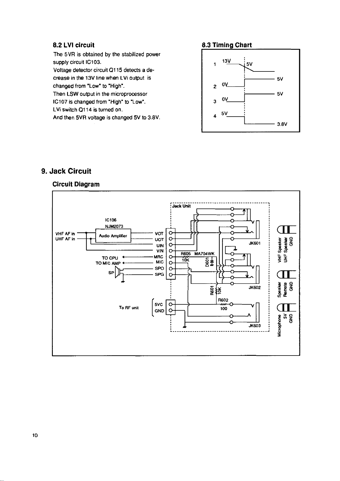
8.2 LVI circuit
The 5VR is obtained by the stabilized power
supply circuit IC103.
Voltage detector circuit Q115 detects a de
crease in the 13V line when LVi output is
changed from "Low" to "High".
Then LSW output in the microprocessor
IC107 is changed from "High" to "Low".
LVi switch Q114 is turned on.
And then 5VR voltage is changed 5V to 3.8V.
9. Jack Circuit
Circuit Diagram
8.3 Timing Chart
Jack Unit
VHF AF in
UHF AF in
Audio Amplifier
I
TO CPU
TO MIC AMP
IC106
NJM2073
SP
> r
To RF unit
VOT
UOT
UIN
VIN
MRC
MIC
SPO
SPG
SVC
GND
a
a
o
o
R605 MA704WK
o
10K
o
a
o
100
JK601
JK602
JK603
cn
II I
« M O
w w
cm
I I I
s e o
W i t
C EE
a > a
e m z
10
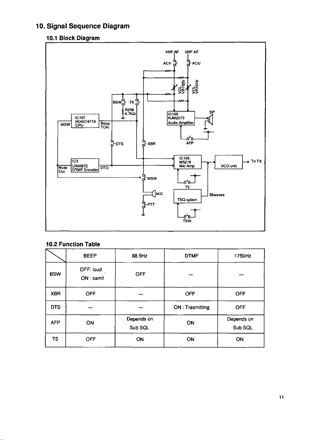
10. Signal Sequence Diagram
10.1 Block Diagram
VHFAF UHFAF
TSW
11
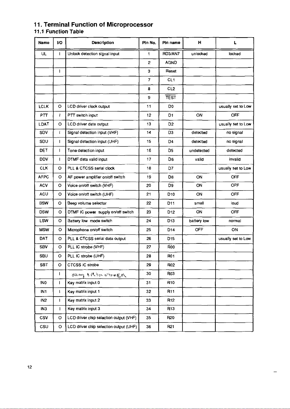
11. Terminal Function of Microprocessor
11.1 Function Table
Name
UL I
LCLK 0
PTT
LDAT 0
SDV
SDU I Signal detection input (UHF)
DET t Tone detection input 16
DDV I
CLK
AFPC 0
I/O
Unlock detection signal input
I 3
LCD driver clock output
I PTT switch input 12
LCD driver data output
Signal detection input (VHF)
I
DTMF data valid input
0 PLL & CTCSS serial clock
AF power amplifier on/oft switch
Description
Pin No.
Pin name H
1
RD3/AN7
unlocked locked
L
2 AGND
Reset
7 CL1
8 CL2
9 TEST
11
13
14
15
17
18
19 D8 ON OFF
DO
D1
D2
D3 detected
D4
D5 undetected
D6 valid invalid
D7
ON
detected
usually set to Low
OFF
usually set to Low
no signal
no signal
detected
usually set to Low
ACV 0
ACU
BSW
DSW 0
LSW
MSW 0 Microphone on/off switch
DAT
SBV
SBU 0
SBT
INO I
IN1 I Key matrix input 1 32 R11
IN2 I
IN3
CSV 0
Voice on/oft switch (VHF) 20
Voice on/off switch (UHF)
0
0 Beep volume selector
DTMF IC power supply on/off switch
Battery low mode switch 24
0
PLL & CTCSS serial data output 26 D15 usually set to Low
0
PLL IC strobe (VHF)
0
PLL IC strobe (UHF)
CTCSS IC strobe
0
I
ijCCfcrfj tfho -JI ^ r i \
Key matrix input 0
Key matrix input 2
Key matrix input 3 34 R13
I
LCD driver chip selection output (VHF)
21
22
23
25
27
28 R01
29
30 R03
31
33
35 R20
D9
D10 ON OFF
D11
D12
D13
D14
R00
R02
R10
R12
ON
small
ON
battery low
OFF
OFF
loud
OFF
normal
ON
12
CSU 0
LCD driver chip selection output (UHF)
36
R21
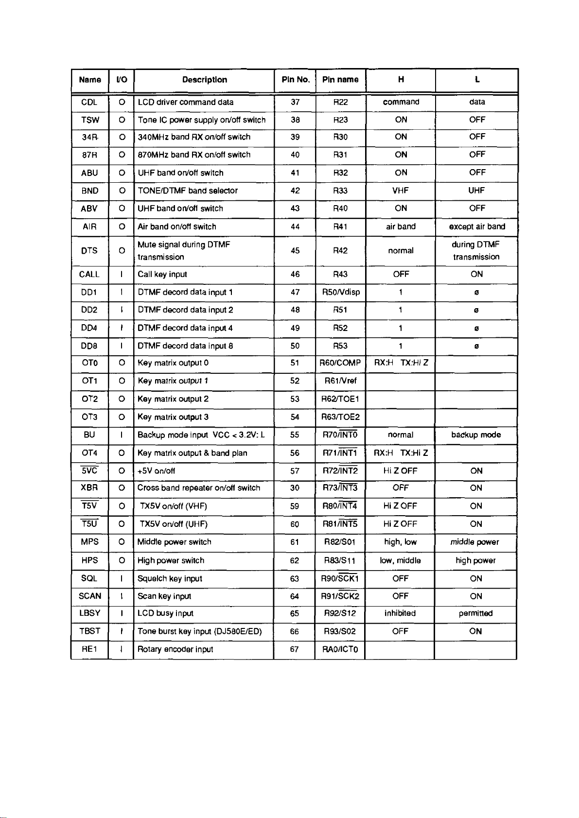
Name I/O
Description
Pin No.
Pin name
H L
CDL o LCD driver command data 37 R22
TSW
34 R. o
87R
ABU
BND
ABV
AIR o Air band on/off switch 44 R41
DTS 0
CALL I Call key input 46 R43 OFF
DD1
DD2
DD4
DD8
OTO
OT1
o Tone IC power supply on/off switch 38 R23
340MHz band RX on/off switch
o
870MHz band RX on/off switch
39 R30
40 R31
o UHF band on/off switch 41 R32
o TONE/DTMF band selector 42
0 UHF band on/off switch 43 R40
Mute signal during DTMF
transmission
DTMF decord data input 1
I
I
DTMF decord data input 2
I
DTMF decord data input 4
I
DTMF decord data input 8
0 Key matrix output 0 51
Key matrix output 1
0
45 R42
47 R50/Vdisp 1 0
48 R51 1 0
49
50 R53 1 0
52
R33
R52 1 0
R6O/COMP
R6l/Vref
command data
ON OFF
ON
ON
ON OFF
VHF
ON
air band
normal
RX:H TX:H/Z
OFF
OFF
UHF
OFF
except air band
during DTMF
transmission
ON
OT2
OT3 o Key matrix output 3 54 R63/TOE2
BU I Backup mode input VCC < 3.2V: L 55 R70/INT0 normal
OTA 0
5VC o
XBR o Cross band repeater on/oft switch 30
T5V
T5U
MPS 0
HPS 0
SQL
SCAN
LBSY
TBST I
RE1
o Key matrix output 2
Key matrix output & band plan
+5V on/off
TX5V on/off (VHF)
0
TX5V on/off (UHF)
0
Middle power switch
High power switch
Squelch key input
I
I Scan key input 64
LCD busy input
I
Tone burst key input (DJ580E/ED)
Rotary encoder input
I
53 R62/TOE1
56 R71/INT1
57 R72/INT2 Hi Z OFF ON
RX:H TX:HiZ
R73/INT3 OFF
59
60
61 R82/S01
62 R83/S11 low, middle high power
63 R90/SCK1
65 R92/S12 inhibited permitted
66 R93/S02
67
R80/1NT4 Hi Z OFF
R81/INT5 Hi Z OFF ON
high, low
OFF ON
R91/SCK2
RA0/I CTO
OFF ON
OFF
backup mode
ON
ON
middle power
ON
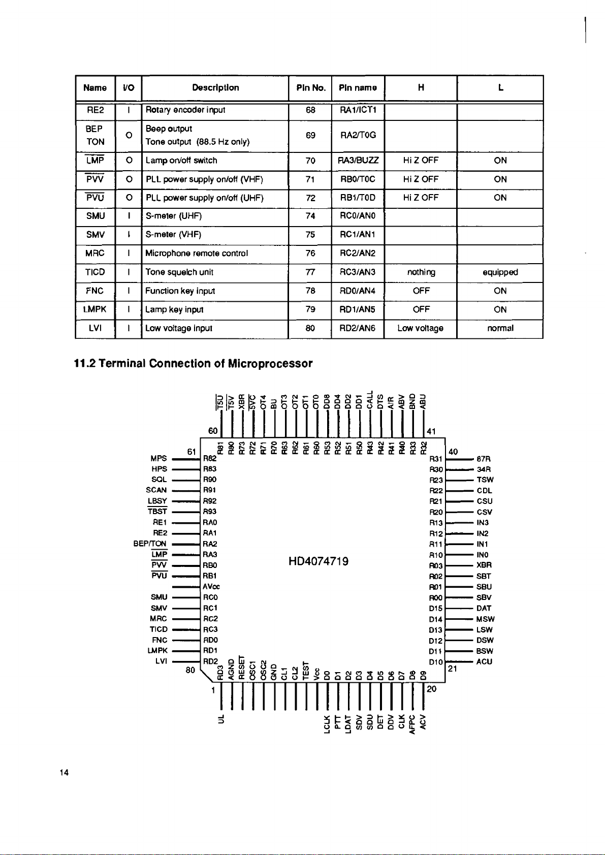
Name I/O
Description
Pin No.
Pin name
H L
RE2 I
BEP
TON
LMP
PVV 0
PVU
SMU
SMV
MRC I
Rotary encoder input
Beep output
0
Tone output (88.5 Hz only)
0 Lamp on/oft switch
PLL power supply on/off (VHF)
0
PLL power supply on/off (UHF)
I
S-meter (UHF)
l S-meter (VHF)
68
69
70
71
72
74
75
Microphone remote control 76 RC2/AN2
RA1/ICT1
RA2/T0G
RA3/BUZZ
RB0/T0C
RB1/T0D
RC0/AN0
RC1/AN1
Hi 2 OFF
Hi 2 OFF
Hi Z OFF
TICD I Tone squelch unit 77 RC3/AN3 nothing
FNC
LMPK I
LVI
I
Function key input
Lamp key input
I Low voltage input 80 RD2/AN6 Low voltage normal
78
79
RD0/AN4
RD1/AN5
11.2 Terminal Connection of Microprocessor
K i m > h 3 t t t t Q û û û < i - E m z i £ |
h h x S O cdO O O O û û û û o û < - 5 oû!S
OFF
OFF
ON
ON
ON
equipped
ON
ON
MPS
H PS
SQL
SCAN
LBSY
TBST
RE1
RE2
BEP/TON
LMP
PW
PVU
SMU
SMV
MRC
TICD
FNC
LMPK
LVI
60
CD 3 S N S
CC CC CC CC Œ
61
R02
R83
R90
R91
R92
R93
RAO
RA1
RA2
RA3
RBO
RB1
AVcc
RCO
RC1
RC2
RC3
RDO
RD1
RD2 Q tü T - cm
80
« 2 W O O
V O 0 lu
X Π< CC
1
Q <7) CM
CC ΠCC
HD4074719
û (\J
Z j J üj
O O O K
<0
’- Q n o j i - Q r ï W f - o n w
( T Œ Œ Œ Œ Œ £ i r ( r £ Œ Œ
in (c r» o>
S
Û 5 û û Q
41
R31
R30
R23
R22
R21
R20
R13
R12
R11
R10
R03
R02
R01
noo
D15
D14
D13
D12
D11
D10
40
21
07R
34R
TSW
CDL
CSU
CSV
IN3
IN2
IN1
INO
XBR
SBT
SBU
SBV
DAT
MSW
LSW
DSW
BSW
ACU
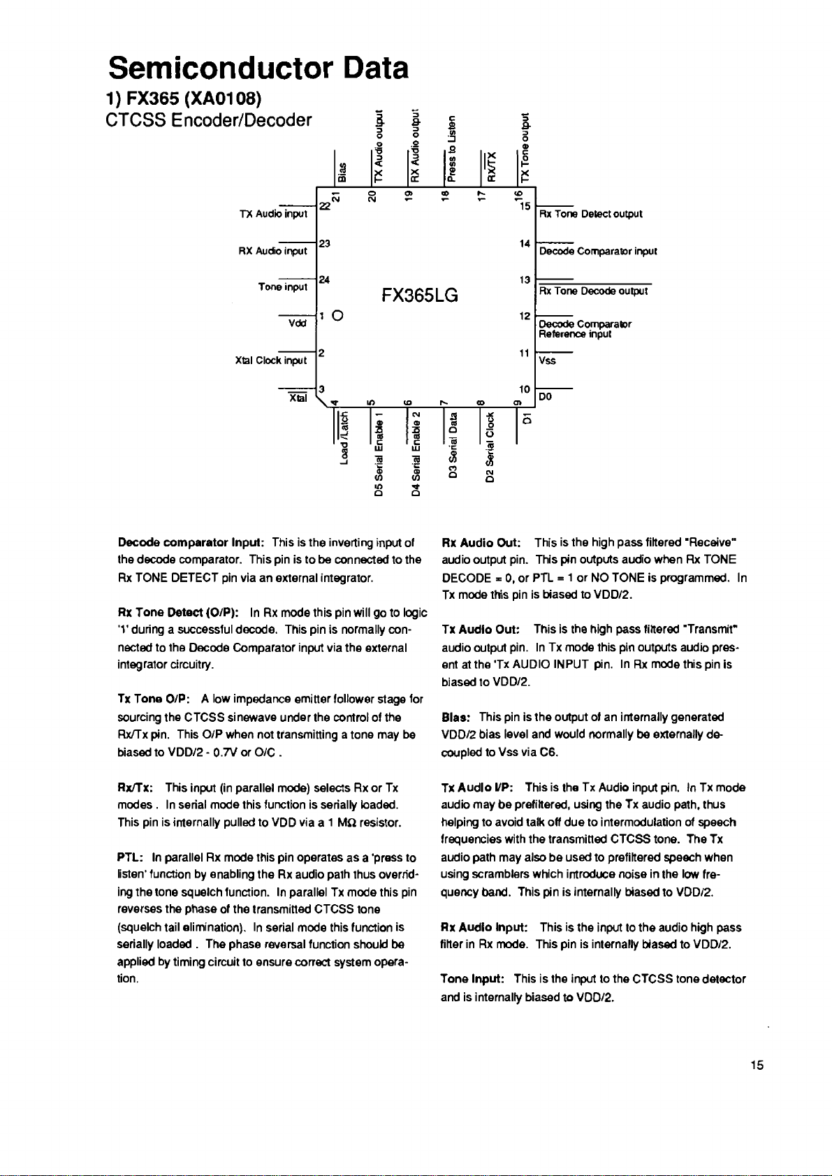
Semiconductor Data
1) FX365 (XA0108)
CTCSS Encoder/Decoder
TX Audio input
RX Audio input
Tone input
Vdd
Xtal Clock input
___ 3
Xtal X
22
23
24
1 O
I
O
'O
<
Bias
£
3
&
3
3
o
O
o
X
£E
FX365LG
B
:□
3
a.
c
in
<0
V)
Ife
S
a:
15
Rx Tone Detect output
14
Decode Comparator input
13
Rx Tone Decode output
12
Decode Comparator
Reference input
11
Vss
10
DO
Decode comparator Input: This is the inverting input of
the decode comparator. This pin is to be connected to the
Rx TONE DETECT pin via an external integrator.
Rx Tone Detect (O/P): In Rx mode this pin will go to logic
’V during a successful decode. This pin is normally con
nected to the Decode Comparator input via the external
integrator circuitry.
Tx Tone O/P: A low impedance emitter follower stage for
sourcing the CTCSS sinewave under the control of the
Rx/Tx pin. This O/P when not transmitting a tone may be
biased to VDD/2 - 0.7V or O/C .
Rx/Tx: This input (in parallel mode) selects Rx or Tx
modes . In serial mode this function is serially loaded.
This pin is internally pulled to VDD via a 1 M il resistor.
PTL: In parallel Rx mode this pin operates as a 'press to
listen' function by enabling the Rx audio path thus overrid
ing the tone squelch function. In parallel Tx mode this pin
reverses the phase of the transmitted CTCSS tone
(squelch tail elimination). In serial mode this function is
serially loaded . The phase reversal function should be
applied by timing circuit to ensure correct system opera
tion.
Rx Audio Out: This is the high pass filtered "Receive1'
audio output pin. This pin outputs audio when Rx TONE
DECODE - 0, or PTL = 1 or NO TONE is programmed. In
Tx mode this pin is biased to VDD/2.
Tx Audio Out: This is the high pass tittered "Transmit"
audio output pin. In Tx mode this pin outputs audio pres
ent at the'Tx AUDIO INPUT pin. In Rx mode this pin is
biased to VDD/2.
Bias: This pin is the output of an internally generated
VDD/2 bias level and would normally be externally de
coupled to Vss via C6.
Tx Audio l/P: This is the Tx Audio input pin. In Tx mode
audio may be prefiltered, using the Tx audio path, thus
helping to avoid talk off due to intermodulation of speech
frequencies with the transmitted CTCSS tone. The Tx
audio path may also be used to prefiltered speech when
using scramblers which introduce noise in the low fre
quency band. This pin is internally biased to VDD/2.
Rx Audio Input: This is the input to the audio high pass
filter in Rx mode. This pin is internally biased to VDD/2.
Tone Input: This is the input to the CTCSS tone detector
and is internally biased to VDD/2.
15
2) LR40872 (XA0042)
Tone Dialer
Test Circuit
3.5-10V
3.58 MHz J T
J
LR40872
------
1 18
2 17
3 16
4 15
5 14
6 13
7 12
8 11
9 10
Row Tone 400mV rms
ColumnTone 500mV rms
F
f1=697Hz
12=770Hz
f3=852Hz
f4=941 Hz
f5=1209Hz
f6=1336Hz
f7=1477Hz
f8=1633Hz
V + l=
v+ d
XMRT 1—
Switch —
COL1 d
COL2 [ =
C O L 3 ^
V - [=
OSCin d
OSCout
1
2
3
4
5
6
7
8
9
18
^□ N on Connect
17
1 Tone out
16
__J Single Tone inhibit
15
14
^ R O W 2
13
ZDRO W3
^ R O W 4
12
^□ M ute Out
11
Z U COL4
10
ROW1
f—
.R40872
3) M5218FP (XA0006)
Dual Low Noise
Operational Amplifiers
4) M67748L (XA0148)
135 - 150MHz 7W
RF Power Module
Output 1 1
Inverting Input 1 2
Non Inverting Input 1 3
Power Supply Minus 4
Power Supply Plus
= 3 8
Output 2
r ^ 7
Inverting Input 2
= 1 6
Non Inverting Input 2
= 3 5
16
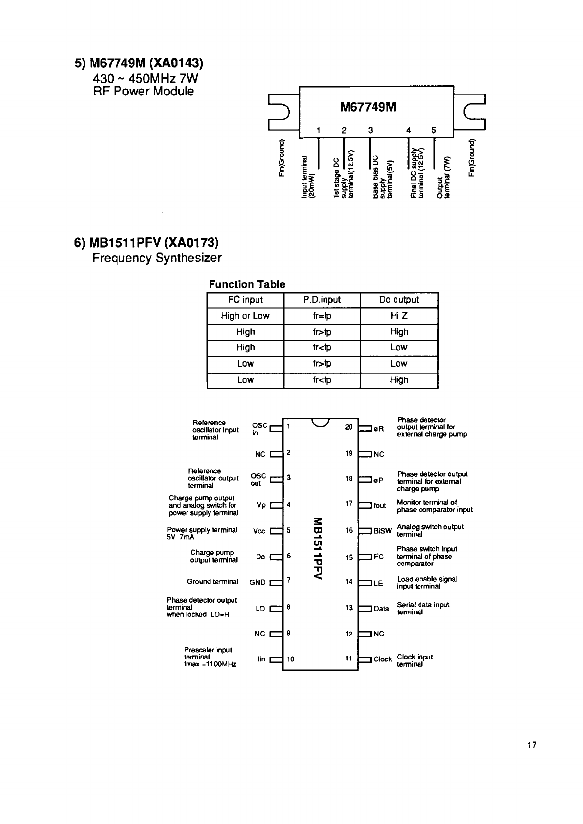
5) M67749M (XA0143)
430- 450MHz 7W
RF Power Module
6) MB1511PFV (XA0173)
Frequency Synthesizer
Function Table
FC input
P.D.input Do output
High or Low fr=fp HiZ
High
fr>fp
High
High fr<fp Low
Low
fr>fp
Low
Low fr<fp High
Fin(Ground)
Referenoe OSC
oscillator input ¡n I
terminal
Reference
oscillator output o s c
terminal out
Charge pump output
and analog switch for
power supply terminal
Power supply terminal
5V 7mA
Charge pump
output terminal
Ground terminal GND
Phase detector output
terminal
when locked :LD=H
Prescaler input
terminal
fmax =1100MHz
NC
Vcc
Do
LD
NC
Vp
1
2
3
4
3
5
00
cn
6
■O
5
7
8
9
fin
10
20
19
18
17
16
15
14
13
12
11
ZZI 0R
! □ NC
Z D aP
H 3 BiSW
Z Z iF C
ZZ I LE
— 1 NC
— 1 Clock
Phase detector
output terminal for
external charge pump
Phase detector output
terminal lor external
charge pump
Monitor terminal of
i tout
phase comparator input
terminal
Phase switch input
terminal of phase
comparator
input terminal
1 Data
terminal
terminal
17
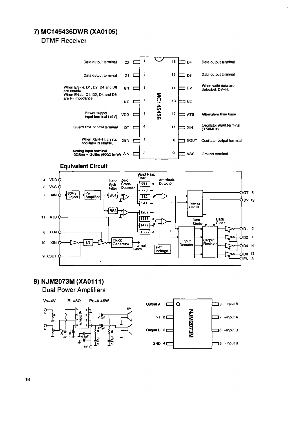
7) MC145436DWR (XA0105)
DTMF Receiver
Data output terminal D2
Data output terminal D1
When EN=H, D1, D2, D4 and D8 en
are enable.
When EN=L, D1, D2, D4 and D8
are Hi-impedance.
Rower supply VDD
input terminal (+5V) vw
Guard time control terminal GT
When XEN=H, crystal ^EN
oscillator is enable.
Analog input terminal
-32dbfn~-2dBm{600Q1mW) AIN
Equivalent Circuit
NC
1 ^ 1.
2 15
3 14
s
4 O 13
cn
5 È 12
O)
6 11
7 10
8 9
= ) D4
m D8
! □ DV
Z 3 NC
ATB Alternative time base
Z D ATB
— 1 XIN
XOUT Oscillator output terminal
Z 3 XOUT
VSS Ground terminal
Z D v ss
Data output terminal
Data output terminal
When valid data are
detected, DV=H.
Oscillator input terminal
(3.58MHz)
GT 5
DV 12
8) NJM2073M (XA0111)
Dual Power Amplifiers
Vs=4V
RL=Bft Po=0.46W
D1 2
D2 1
D4 14
D8 13
EN 3
Output A 1
18
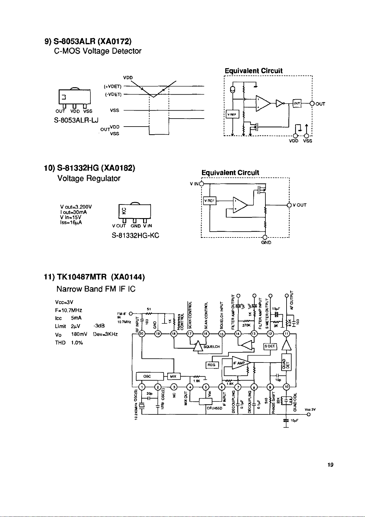
9) S-8053ALR (XA0172)
C-MOS Voltage Detector
VDD
10) S-81332HG (XA0182)
Voltage Regulator
V out=3.200V
I out*30mA
V in=15V
lss=16^iA
u u u
VOUT GND V IN
S-81332HG-KC
Equivalent Circuit
Equivalent Circuit
11) TK10487MTR (XA0144)
Narrow Band FM IF IC
Vcc=3V
F=10.7MHz
Ice 5mA
Limit 2nV -3dB
Vo 180mV Dev=3KHz.
THD 1.0%
22
19
CL2( Clock) —
SYNC(Syncronous) —
Vlc1 (LCD power supply) —
Vlc2(LCD power supply) —
Vlc3(LCD power supply) —
Vss(Ground) —
Vdd(+5V) —
SCK(Serial Clock) —
SI(Serial input) —
CS(Chip Select) —
BUSY—
C / D(Command or Data) —
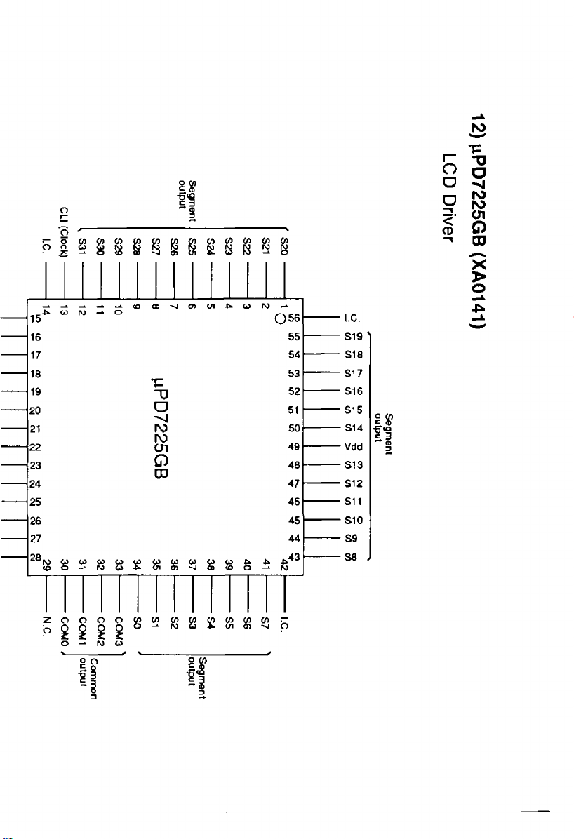
12) HPD7225GB (XA0141)
LCD Driver
sie
î i
«
I.e .
S19
S18
S17
S16
S15
2 8 ?
S14
l !
Vdd
S13
S12
S11
S10
S9
S8
o O
£. o
n
t i
 Loading...