KAWA ELECTRONIC RESEARCH & DEVELOPMENT CENTRE
Service Manual
Reference No.
Revision
Date
Page
In House Model No.
Customer Model No.
BOM No
Description
Prepared By:
Checked By: Electronic Engineer
SM- PDP50HADSE-001
0
2006.Nov.
P .lo f 96
PDP50HAP
: PDP5016H
: PDP50HADSE-A01
Service Manual for PDP5016H S50HW-XD03 USA
Mechanical Engineer
Approved By: Engineering Manager
Received By: MK Department
DOC Rev
NO.
0
Initial Release
The Latest Revision Details DATE
t .
2006-Nov-iJ
AKAI
SERVICE MANUAL
Model: PDP5016H
1. S afety Instructions............................................................................................................1 ~2
2. Product Specification.......................................................................................................3—11
3. Block Diagram................................................................................................................12—13
4. Circuit Diagram...............................................................................................................14—3 6
5. Basic Operation & Circuit Description..........................................................................37—41
6. Main IC Information....................................................................................................... 42—50
7. Panel Information............................................................................................................51—87
8. Explored View................................................................................................................88
9. Spare Pare List................................................................................................................89—92
10. If you forget your V-chip password
11. Software Upgrade............................................................................................................94
.............................................................................. 93
This manual is the latest at the time of printing, and does not
include the modification which may be made after the printing,
by the constant improvement of product.

Safety Precaution
CAUTION
RISK OF ELECTRIC SHOCK
DO NOT O PEN
A
CAUTION: TO REDUCE THE RISK OF
ELECTRIC SH OCK, DO NOT REMOVE COVER
(OR BACK). NO USER-SERVICEABLE PARTS
INSIDE. REFER SERVICING TO QUALIFIED
SERVICE PERSONNEL ONLY.
A
The lightning flash with arrowhead symbol,
within an equilateral triangle, is intended to
alert the user to the presence of uninsulated
“dangerous voltage” within the product’s enclo
sure that may be of sufficient magnitude to
constitute a risk of electric shock to persons.
The exclamation point within an equilateral
triangle is intended to alert the user to the
presence of important operating and
maintenance (servicing) instructions in the
literature accompanying the appliance.
PRECAUTIONS DURING
SERVICING
1. In addition to safety, other parts and
assemblies are specified for conformance with
such regulations as those applying to spurious
radiation. These must also be replaced only
with specified replacements.
Examples: RF converters, tuner units, antenna
selection switches, RF cables, noise-blocking
capacitors, noise-blocking filters, etc.
2. Use specified internal Wiring. Note especially:
1) Wires covered with PVC tubing
2) Double insulated wires
3) High voltage leads
3. Use specified insulating materials for hazardous
live parts. Note especially:
1) Insulating Tape
2) PVC tubing
3) Spacers (insulating barriers)
4) Insulating sheets for transistors
5) Plastic screws fo r fixing micro switches
4. When replacing AC primary side components
(transformers, power cords, noise blocking
capacitors, etc.), wrap ends of wires securely
about the terminals before soldering.
5. Make sure that wires do not contact heat
generating parts (heat sinks, oxide metal film
resistors, fusible resistors, etc.)
6. Check if replaced wires do not contact sharply
edged or pointed parts.
7. Make sure that foreign objects (screws, solder
droplets, etc.) do not remain inside the set.
MAKE YOUR CONTRIBUTION
TO PROTECT THE
ENVIRONMENT
Used batteries with the ISO symbol
\5<9
for recycling as well as small accum ulators
(rechargeable batteries), mini-batteries (cells) and
starter batteries should not be thrown into the
garbage can.
Please leave them at an appropriate depot.
WARNING:
Before servicing this TV receiver, read the
SAFETY INSTRUCTION and PRODUCT
SAFETY NOTICE.
SAFETY INSTRUCTION
The service should not be attempted by anyone
unfam iliar with the necessary instructions on this
apparatus. The following are the necessary
instructions to be observed before servicing.
1. An isolation transformer should be connected in
the power line between the receiver and the
AC line when a service is performed on the
prim ary of the converter transformer of the set.
2. Comply with all caution and safety related
provided on the back of the cabinet, inside the
cabinet, on the chassis or picture tube.
3. To avoid a shock hazard, always discharge the
picture tube's anode to the chassis ground
before removing the anode cap.
4. Completely discharge the high potential voltage
of the picture tube before handling. The picture
tube is a vacuum and if broken, the glass will
explode.
1/ 94

5. When replacing a MAIN PCB in the cabinet,
always be certain that all protective are
installed properly such as control knobs,
adjustm ent covers or shields, barriers, isolation
resistor networks etc.
6. When servicing is required, observe the original
lead dressing. Extra precaution should be given
to assure correct lead dressing in the high
voltage area.
7. Keep wires away from high voltage or high
tempera ture components.
8. Before returning the set to the customer,
always perform an AC leakage current check
on the exposed metallic parts of the cabinet,
such as antennas, terminals, screwheads, metal
overlay, control shafts, etc., to be sure the set
is safe to operate without danger of electrical
shock. Plug the AC line cord directly to the
AC outlet (do not use a line isolation
transformer during this check). Use an AC
voltmeter having 5K ohms volt sensitivity or
more in the following manner.
Connect a 1.5K ohm 10 watt resistor paralleled
by a 0.15pF AC type capacitor, between a
good earth ground (water pipe, conductor etc.,)
and the exposed metallic parts, one at a time.
Measure the AC voltage across the combination
of the 1.5K ohm resistor and 0.15 uF
capacitor. Reverse the AC plug at the AC
outlet and repeat the AC voltage measurem ents
for each exposed metallic part.
The measured voltage must not exceed 0.3V
RMS.
This corresponds to 0.5m A AC. Any value
exceeding this limit constitutes a potential
shock hazard and must be corrected
immediately.
The resistance measurem ent should be done
between accessible exposed metal parts and
power cord plug prongs with the pow er switch
"ON". The resistance should be more than
6M ohms.
AC VOLTMETER
PRODUCT SAFETY NOTICE
Many electrical and m echanical parts in this
apparatus have special safety-related
characteristics.
These characteristics are offer passed
unnoticed by visual spection and the protection
afforded by them cannot necessarily be obtained
by using replacement components rates for a
higher voltage, wattage, etc.
The replacement parts which have these
special safety characteristics are identified by A
marks on the schematic diagram and on the parts
list.
Before replacing any of these components,
read the parts list in this manual carefully. The
use of substitute replacement parts which do not
have the same safety characteristics as specified
in the parts list may create shock, fire, or other
hazards.
9. Must be sure that the ground wire o f the AC
inlet is connected with the ground of the
apparatus properly.
Good earth ground
such as the water
- pipe, conductor,
etc.
AC Leakage Current Check
1500 ohmi, lOwatt
Place this probe
on each exposed
metallic part
2/ 94
Technical Specifications
M O D E L i PDP-5G16
5 0 ” P la s m a D is p la y
DATE FIRST ISSUED ISSUE
1
REVISIONS
ISSUED DATE DESCRIPTION RAISED BY i
RAISED BY CHECKED BY NUMBER OF PAGES
9
SPECIFICATION AGREED : SIGNATURE DATE
R & D DEPARTMENT
COMMERCIAL DEPARTMENT
PRODUCTION DEPARTMENT
Q/A DEPARTMENT
CUSTOMER
SPECIFICATION APPROVED : SIGNATURE : DATE
NOTE : Only d o cu m e nts sta m p ed “Co n tr o lled D o c u m en t” to b e u sed fo r m a nu factu r e of p rod u c tion p arts.
3/ 94

CONTINUATION PAGE
Technical Specifications
1. S ta n d a r d T e s t C o n d itio n s
PDP-5016
NUMBER 2 OF 9 PAGES
All tests shall be performed under the following conditions, unless otherwise specified.
1.1 Ambient light
1.2 Viewing distance
1.3 Warm up time
1.4 PDP Panel facing
1.5 Measuring Equipment
1.6 Magnetic field
1.7 Control settings
1.8 Power input
1.9 Ambient temperature
1.10 Display mode
150ux (When measuring IB, the ambient luminance
= 0.1Cd/m2)
50cm in front of PDP
30 minutes
no restricted
PC, Chroma 2225 signal generator (with Chroma digital
additional card) or equivalent, Minolta CA100 photometer
no restricted
Brightness, Contrast, Tint, Color set at Center(50)
100~240Vac
20°C ± 5°C (68°F ± 9°F)
31.5KHz/60Hz (Resolution 1366 x 768)
1.11 Other conditions
1.11.1 With image sticking protection of PDP module, the luminance will descend
by time on a same still screen and rapidly go down in 5 minutes. When
measuring the color tracking and luminance of a same still screen, be sure t
o accomplish the measurement in one minute to ensure its accuracy.
1.11.2 Due to the structure of PDP, the extra-high-bright same screen should not
hold over 5 minutes for fear of branding on the panel.
4/ 94

Technical Specifications
E L E C T R IC A L C H A R A C T E R IS T IC S
2. P o w e r In p u t
PDP-5016
CONTINUATION PAGE
NUMBER 3 OF 9 PAGES
2.1 Voltage
2.2 Input Current
2.3 Maximum Inrush Current
Test condition
2.4 Frequency
2.5 Power Consumption
Test condition
2.6 Power Factor
2.7 Withstanding voltage
3. D is p la y
3.1 Screen Size
3.2 Aspect Ratio
3.3 Pixel Resolution
3.4 Peak Brightness
3.5 Contrast Ratio (Dark room)
3.6 Viewing Angle
3.7 OSD language
100 ~ 240VAC
5.0 /2.5A
<30 A (FOR AC110V ONLY)
Measured when switched off for at least 20 mins
50Hz to 60Hz(±3Hz)
< 480W
full white display with maximum brightness and
contrast
Meets I EC 1000-3-2
1.5kVac or 2.2kVdc for 1 sec
50” Plasma display
16:9
1366x768
1000 cd/m2 (Panel module without filter)
4000:1 (Panel module without filter)
Over 160°
English
4. S ig n al
4.1 TV/AV & Graphic input
4.1.1 TV standard
4.1.2 TV Tuning system
4.1.3 CATV
4.1.4 Composite signal
4.1.5 Y,C Signal
4.1.6 Component signal
4.1.7 Graphic I/P
4.1.8EDID compatibility
4.1.9 I/P frequency
NTSCM,PAL/N,PAL/M
PLL 181CH
125CH
CVBS
S-Video
Y, Pb/Cb, Pr/Cr, HDTV compatible
Analog: D-sub 15pin detachable cable
Digital: DVI
DDC 1.3
fH 31.5kHz to 60kHz/fV: 56.25Hz to 75Hz (1024X768
recommended)
5/ 94

Technical Specifications
4.2 Audio input
Audio I/P(L/Rx5)
4.3 AV output
Audio&Video O/P(RCAx3)
PDP-5016
1 for DVI / D-Sub
1 for Y/ Pb/Pr
1 for Y/ Cb/Cr
1 for CVBS
1 for S-Video
: Monitor out(Video & Audio L/R)
CONTINUATION PAGE
NUMBER 4 OF 9 PAGES
4.4 Other function :
5. E n v ir o n m e n t
5.1 Operating environment
5.1.1 Temperature :
5.1.2 Relative humidity:
5.2 Storage and Transport
5.2.1 Temperature :
5.2.2 Relative humidity:
6. P a n e l C h a r a c te r is tic s
6.1 Type
6.2 Size
6.3 Aspect ratio
6.4 Viewing angle
6.5 Resolution
6.6 Weight
6.7 Color
6.8 Contrast
6.9 Peak brightness :
PIP/POP/PBP, Picture size, Picture Still, Sound mode,Last
memory, Timer, MTS
5° to 33°C
20% to 85%(non-condensing)
-20°C to 60°C(-4° to 140°F)
5% to 95%
S50HW-XD03
50”, 1190mm(width)x7005mm(height)x59mm(depth)±1
mm)
16:9
Over 160°
1366X768
22.0kg ±0.5 kg (Net)
1024(R)X1024(G)X1024(B) COLORS
Average 60:1 (In a bright room with 150Lux at center)
Typical 5000:1 (In a dark room 1/100 White Window
pattern at center).
Typical 1000cd/m2 (1/25 White Window)
6.10 Color Coordinate Uniformity :
Test Pattern :
Contrast; Brightness and Color control at norma
setting
Full white pattern
Average of point A,B,C,D and E +/- 0.01
6/ 94

Technical Specifications
PDP-5016
NUMBER 5 OF 9 PAGES
6.11 Color temperature : Contrast at center (50); Brightness center (50);
Color temperature set at Natural
x=0.285±0.02
y=0.290±0.02
6.12 Cell Defect Specifications
Subject to Panel supplier specification as appends.
7. F ro n t P an e l C o n t ro l B u tto n
CONTINUATION PAGE
7.1 CH Up / Down Button
Push the key to changing the channel up or down.
When selecting the item on OSD menu.
Volume Up/ Down Button
Push the key to increase the volume up or down.
When selecting the adjusting item on OSD menu
increase or decrease the data-bar.
Menu Button
Source Select Button
7.2 Stand by Button
Enter to the OSD menu.
Push the key to select the input signals source.
Switch on main power, or switch off to enter power
Saving modes.
7.3 Main Power Switch
8. O S D F u n c tio n
Turn on or off the unit.
8.1 Picture : State (Normal,Dark,Bright,User); Display (Bright,contrast,Color,Hue)
Temp (warm,Cool,Normal,User);
Position (H-posit,V-posit,Phase,H-size,Auto Adjust)
8.2 Sound : Setup (Mode,AVC,Volume,Balance);
Equalizer (120HZ,500HZ,1.5KHZ,5KHZ,10KHZ)
BBE Setup (Gain,Treble,Bass)
8.3 OSD : Size (Panorama,16:9,Normal,Anamorphic,Letter Box,TV Mode)
OSD Set (Language,OSD Position,Time Out)
Option (Burn Protect, Version)
V-Chip , C/C
8.4 Layout : Layout (Full Screen,PIP,Split Screen,Grid,POP 3,POP 12)
PIP Set (Sub Win Source,Sub Win Size,PIP Size.PIP Position)
8.5 Time : Sleep (30Min,60Min,90Min,120Min,180Min)
Wake Up (Time Edit,Volume,TV Mode,Channel)
Time Set
8.6 TV Set : TV Set (Auto Search,Manul Search,System,MTS,Auto Fine,Fine)
CH Edit
7/ 94

Technical Specifications
9. A g e n c y A p p r o v a ls
Safety UL60950
Emissions FCC class B
10 . R e lia b ility
PDP-5016
CONTINUATION PAGE
NUMBER 6 OF 9 PAGES
11.1 MTBF
11. A c c e s s o rie s
20,000 hours(Use moving picture signal at 25°C ambient)
User manual x1, Remote control x1, Stand x1, Power cord x1,
Battery x 2, Accessories box x 1 ,Speaker x 2,Speaker wire x2
8/ 94

Technical Specifications
12. Support the Signal Mode
A. D-Sub Mode (VGA or DVI)
PDP-5016
CONTINUATION PAGE
NUMBER 7 OF 9 PAGES
NO.
Resolution
1 640 x 400
2
3
4
5
6
7
8
9
10
11
12
13
14
15
16
17
18
19
640 x 480
640 x 480
640 x 480
640 x 480
720 x 400
800 x 600
800 x 600
800 x 600
800 x 600
832 x 624
1024x 768
1024x 768
1024x 768
1152x 864
1152x 864
1152x 864
1280x 960
1280x 1024
Horizontal
Frequency
Frequency
(KHz)
31.47 70.08
31.50 60.00
35.00 67.00
37.50 75.00
37.86 72.81
31.47 70.08
35.16 56.25
37.90 60.32
46.90 75.00
48.08 72.19
49.00 74.00
48.40 60.00
56.50 70.00
60.00 75.00
54.53 61.13
63.86 70.02
Vertical
(Hz)
Dot Clock
Frequency
(MHz)
25.17
25.18
30.24
31.50
31.50
28.32
36.00
40.00
49.50
50.00
57.27
65.00
75.00
78.75
80.37
94.51
67.52 75.02
60.02 60.02 108.04
64.00 60.01 108.00
108.03
B. DTV Mode
NO. Resolution
1 480 i
2
3
4
5
6
7
8
1080i(1920x1080)
1080i(1920x1080)
576 i
480p(720x480)
576p(720x576)
720p(1280x720)
720p(1280x720)
Horizontal
Frequency
Frequency
(KHz)
15.734 59.94
15.625 50.00
31.468 59.94
31.25 50.00
45.00 60.00
37.50 50.00
28.125 50.00
33.75 60.00
Vertical
(Hz)
Dot Clock
Frequency
(MHz)
13.50
13.50
27.00
27.00
74.25
74.25
74.25
74.25
- When the signal received by the Display exceeds the allowed range, a warning message "Out Of Range”
shall appear on the screen.
- You can confirm the input signal format from the "OSD Menu”.
9/ 94

Technical Specifications
13. R e m o t e C o n tro l
PDP-5016
CONTINUATION PAGE
NUMBER 8 OF 9 PAGES
1 Power ( 6 ): Press to turn on and off.
2 Mute ( ^ ): Press to mute the sound. Press
again or press ► to restore the sound.
3 P.STILL: Press to freeze the picture. Press
again to restore the picture.
4 P.SIZE: Press to cycles through the picture
size: Normal, Fill Screen, Anamorphic,
Letter Box or TV Mode, Panorama..
5 P. MODE: Press to cycles through the
picture mode: Normal, Bright, Dark, User.
6 S.SELE: Press to cycles through the sound
select: Main window sound or Sub window
sound.
7 PIP: Press to turns on PIP (picture-in-
picture) feature. Such as Full Screen, PIP or
Split Screen.
8 SWAP: Press to switches the Main window
or Sub window pictures.
9 PIP CH+ : Press to select Sub window
Channel Up.
PIP CH- : Press to select Sub window
Channel Down.
10 TIME: Press to display the current time.
11 SLEEP: Press repeatedly until it displays
the time in minutes (30 Min, 60 Min, 90 Min,
120 Min, 180 Min or Off ) that you want the
PDP to remain on before shutting off. To
cancel Sleep Time, press SLEEP repeatedly
until Sleep Off appears. And you can press
■4 or ► to select sleep time shut down.
12 MTS: Press repeatedly to cycle through the
Multi-channel TV sound (MTS) options:
Mono, Stereo and SAP (Second Audio
Program).
13 INFO: Press to display on-screen information. Press it again to turn the display off.
14 CH Erase, CH Save buttons: Press to erase or save channel.
10 C/C: Press to select the Closed Caption mode.
10 V-Chip: Press to select the child protect mode.
17 Number buttons: Press 0~9,100 to select a channel; the channel changes after 2
seconds.
10 PIP Source: Press to select the signal for Sub Window.(Only for PIP.)
10 F.WHITE: Press to show a full white picture.
20 PREV: Press it returns to the last viewed channel.(Only for TV.)
1
3
4
7
8
10
11
14
28
-GD
P.STILL P.SIZE P.MODE S.SELE
TZD C 3 c g CZh
O P Q Q
TIME SLEEP
a p æ
Ç 3Ç 3C qC 3-
© © ©
© © ©
© © ©
©
PIP source F.Whlte PREV
O ÇJ Œ l
SOUND PICTURE EXIT
- a □ en im
------
~ ir
100
□
------
15
10/94
(Continued on next page)

CONTINUATION PAGE
Technical Specifications
PDP-5016
NUMBER 9 OF 9 PAGES
21 SOUND: Press to select different sound system, such as Normal, Flat, News, Cinema,
User or BBE Digital.
22 PICTURE: Press to select “BRIGHTNESS”, “COLOR”, “CONTRAST”, ”HUE” or
“SHARPNESS”, and you can use A or ► to adjust.
23 EXIT: Press to return or exit OSD menu.
24 SOURCE: Press to select the signal sources directly. Such as TV, AV1, S-VIDEO,
YCbCr, YPbPr, Analog RGB or Digital RGB.
23 MENU: Press to display the OSD Menu.
23 OK: Press to enter or confirm.
21 ▲ / ▼ : They are used as ▲ / ▼ buttons in the OSD Menu screen and they can be
used for the selection of the program when the OSD Menu is not shown on the screen.
23-4 / ► : They are used as -4 / ► buttons in the OSD Menu screen and they can be
used for the adjustment of volume when the OSD Menu is not shown on the screen.
P H Y S IC A L C H A R A C T E R IS T IC S
14. P o w e r C o r d
Length : 1.8m nominal
Type :
15. C a b in e t
optional
15.1 Color : silver colour as defined by colour plaque reference number
15.2 Weight
Net weight :
Gross weight :
51.8kg
74kg
15.3 Dimensions (w/o stand&handles)
Width :
Height :
Depth :
1227.8mm
739.8mm
122.7mm
11/94
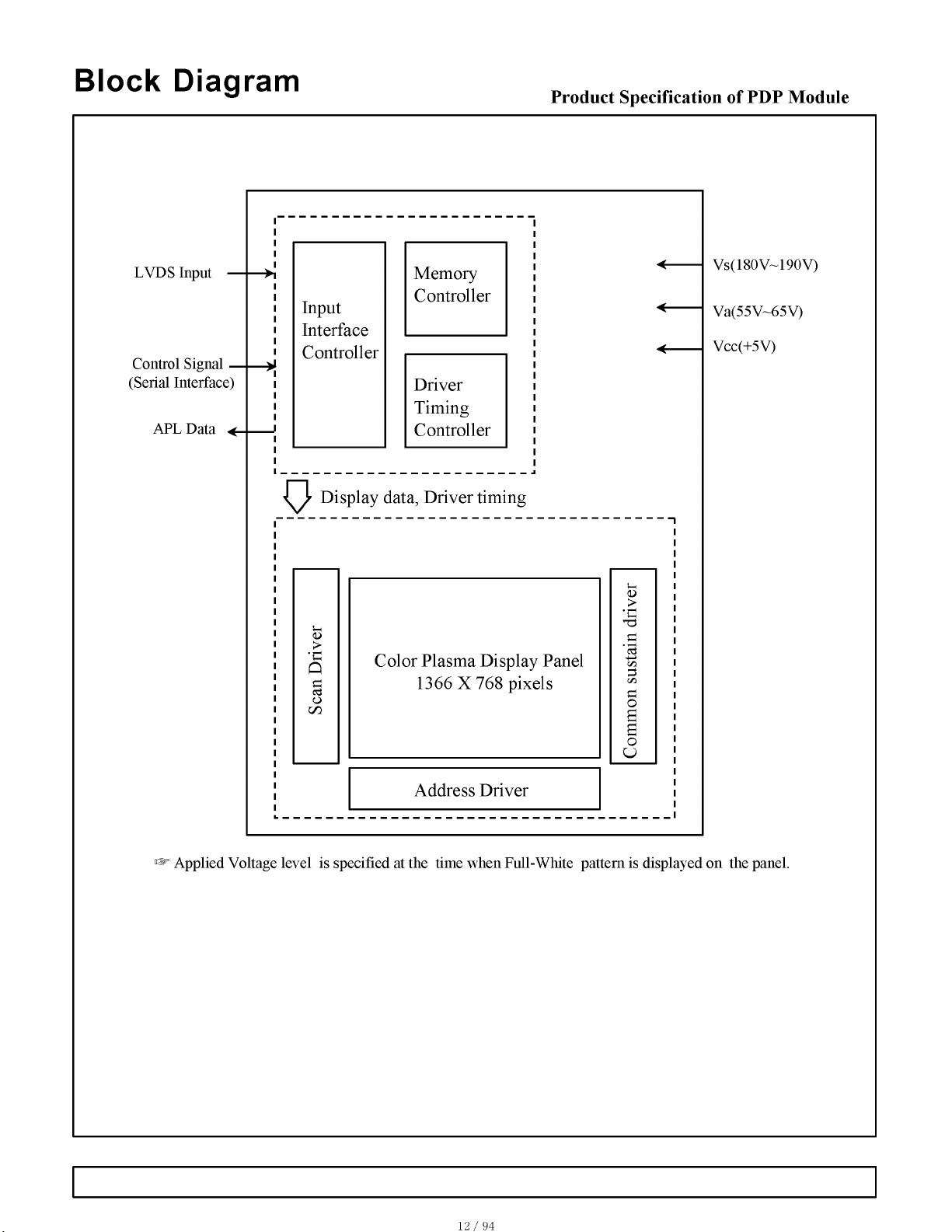
Block Diagram
Product Specification of PDP Module
LVDS Input
Control Signal —
(Serial Interface)
APL Data
Memory
Input
Interface
Controller
Display data, Driver timing
>
•c
Q
G
cd
O
GO
Controller
Driver
Timing
Controller
Color Plasma Display Panel
1366 X 768 pixels
<u
>
•G
T3
cö
3
c
O
a
a
o
O
Vs(180V~190V)
Va(55V~65V)
Vcc(+5V)
Address Driver
Applied Voltage level is specified at the time when Full-White pattern is displayed on the panel.
12/ 94

Block Diag ram MAIN/AUDIO BOARD
13/ 94
Circuit Diagram
- Power supply board o f A u d io A m p lif ier ,
- Main (Vi de o ) board
- A ud i o /T u n e r board
- Ke yp ad b oard
- Remote control rec eiv er board
- Rem ot e contro l board
14/ 94

MP T0 12 A
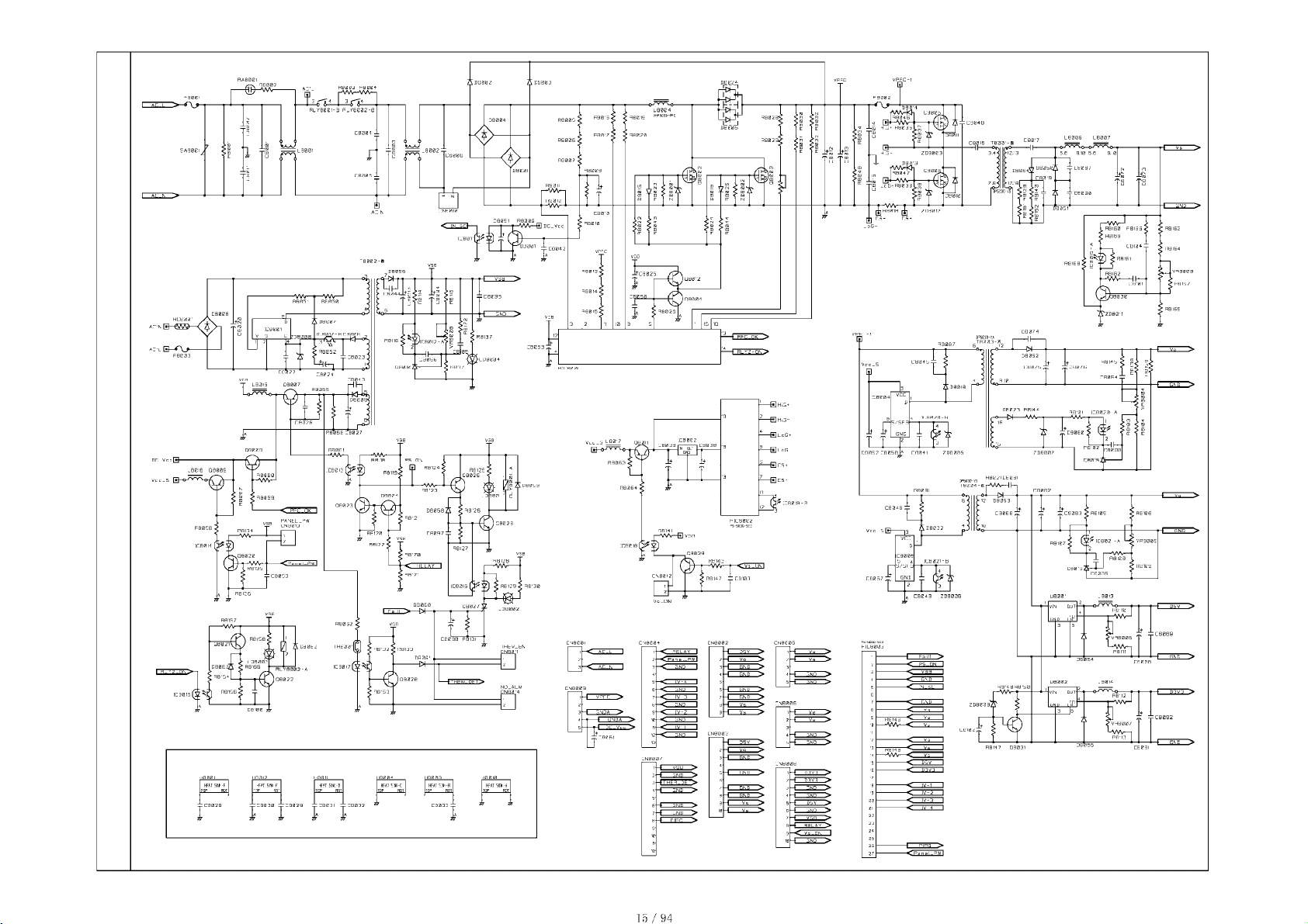
15/94
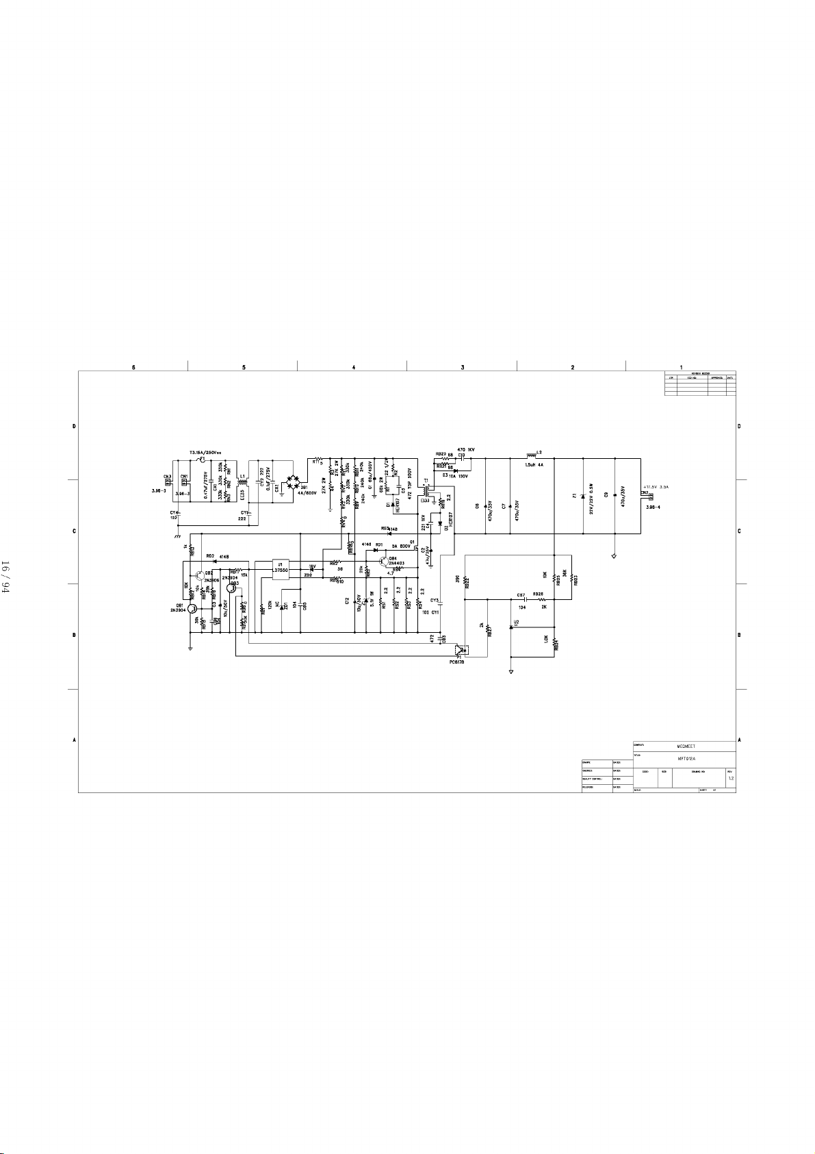
1
16 / 9 4
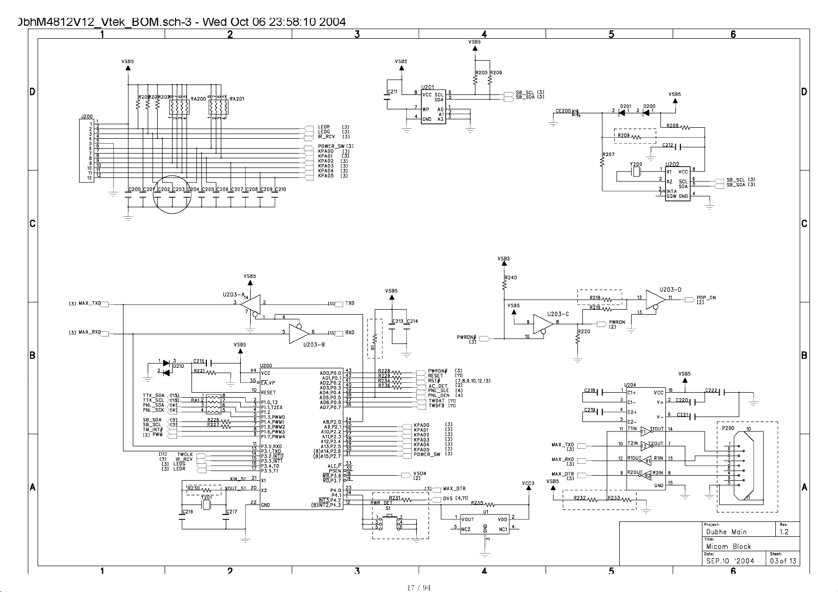
DbhM4812V12 Vtek BOM .sch-3 - Wed Oct 06 23:58:10 2004
17/ 94
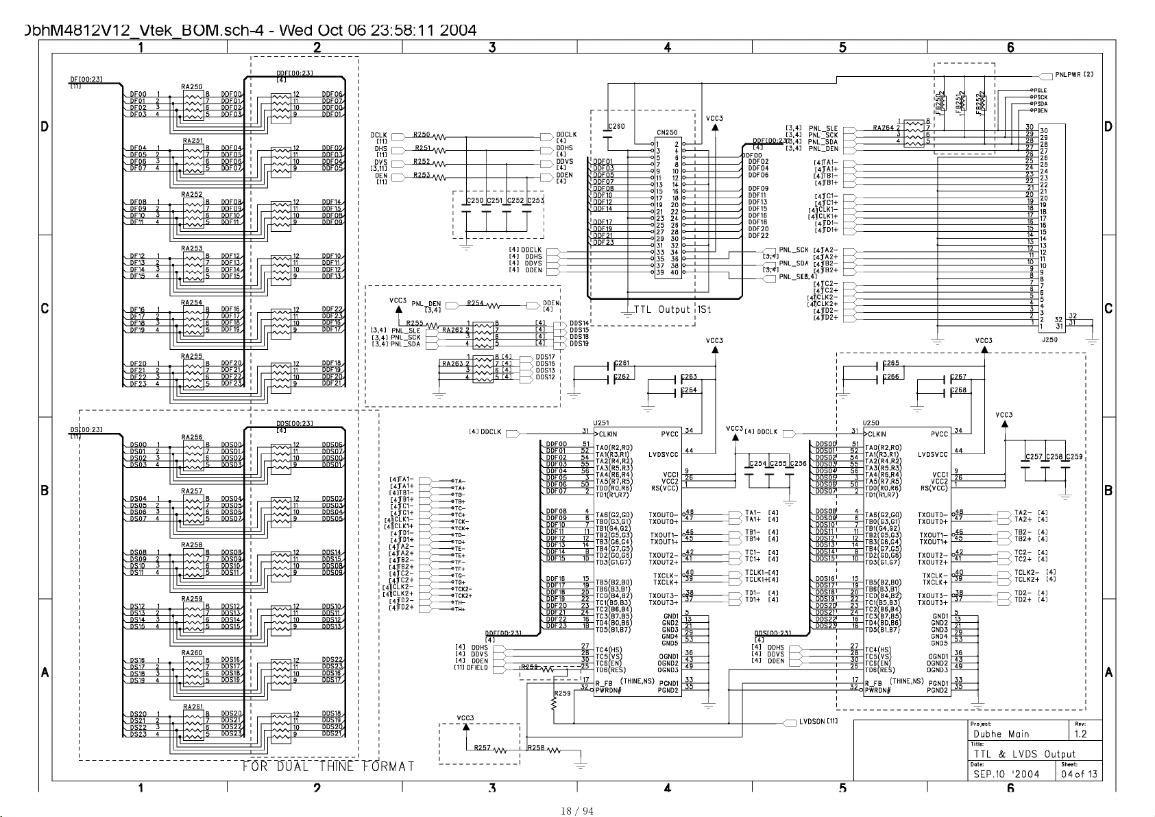
DbhM4812V12 Vtek BOM .sch-4 - Wed Oct 06 23:58:11 2004
DDF[00:23]
~m
------
DDF07/
11
nnFon,
10
DDFOL
9
psbi
. DF04 1
» DF05 ? 7 RDFilfi
„ DFOB 3
» DF07 4
„ DFOB 1
» DF09 7 7 DnFns,
„ dfio 3 B RDF10/
» DF11 4
„ DF17 1
» DF13 7
. HF14 3
» DF15 4
„ DF1B 1
. DF17 2
v DF18 3
„ nFiq 4 5 DDF19,
„ DF70 1
„ DF71 7
v DF22 3
, DF23 4
'S/VS/
I
A252
/wv
'S/VS/
A253
/yvv
/wv
FA254
/yvv
I
FA255
—:
1
b DnF04,
b onFnfi,
5 nnFnz
B DDFOfl.
5 RDF11 .
B DDF17/
7 DHF13/
6 DDF14/
5 DHF15,
R DDF16.
7 DDF17,
R DDF18.
fi DDF20.
7 DDF21,
fi DDF2Z
5 DDF23,
DDF07,
-| 17
IÎDF0.1
11
in DDF04,
nnFos,
DDF14,
I17
imîfis.
in nOFOR,
n0F09,
DDF10/
I17
IÎDF11 ,
in I50F17/
DDF13,
DDF22,
i1?
DDF23,
11
DDF16,
10
DDF17,
DDF18,
l1?
DDF19,
11
DDF20,
10
DDF21,
9
nnsn7.
11
10 nnsoa
nnsm.
nnso7,
I17
nnsn.\
10 ODSfH,
IÎDS05.
9
[4TD1+
nnsu,
I17
DDS15/
10 nnsna,
nnsns,
DDS10,
I17
IÎDR11 ,
10
IÎDS17,
IÎDR1.T,
DDS2Z
I17
DDS23.
DDS16,
10
DDS17,
DDS18.
-|1?
DDS19,
11
DDS20.
10
DDS21,
9
[4 A2-
[4fA2+
[4ÎB2-
[4TB2+
FOR DUAL THINE FORMAT
. DDF01 52
. DDF02 54
. DDF03 55
. DDF04 56
. DDF05 3
. DDF08 50
. DDF07 2
. DDF08 4
. DDF09 6
. DDF10 7
. DDF11
. DDF12 12
. DDF13 14
. DDF14 B
. DDF15 10
. DDF16 15
. DDF17 19
. DDF1B 20
. DDF19 22
. DDF20 23
. DDF21 24
. DDF22 16
. DDF23 1B
11
>CL KIN PVCC
TA0(R2,RD)
TA1(R3,R1)
TA2(R4,R2)
TA3lR5,R3)
TA4(R6,R4) VCC1
TA5(R7,R5) VCC2
TD0(R0,R6) RS(VCC)
TD1(R1,R7)
TA6ÎG2.G0) TXOUTG—
TB0(G3,G1) TXOUTO+
TB1(G4,G2)
TB2(G5,G3) TXOUT1-
TB3 G6.G4) TXOUT14
TB4 G7.G5)
TD2 G0,G6) TXOUT2-
TD3(G1,B7)
TB5(B2,B0)
TB6(B3,B1)
TC0(B4,B2) TX0UT3-
TC1(B5,B3) TX0UT3+
TC2(B6,B4)
TC3 B7.B5) GND1
TD4 B0.B6) GND2
TD5(B1,B7)
TC4(HS)
TC5 VS) 0GND1
TC61EN) 0GND2
TD6(RES) 0GND3
R FB (THINE,NS) PgnD1
PWRDN# PGND2
LVDSVCC
TXOUT2+
TXCLK-
TXCLK+
GND3
GND4
GND5
-R
TA1+
[4]
TB1- [4]
TB1+
[4]
TCI—[4]
TC1+ [4]
TCLK1—[4]
TCLK1-K4]
TD1-
[4]
TD1+
[4]
. DDSOB' 4
. DDS091 6
. DDS101 /
. DDS11 1
. DDS121 17
. DDS131 14
. DDS141 H
. DDS151
. DDS161 15
. DDS171 19
. DDS181 70
. DDS191 22
11
11)
1
>CLKIN PVCC
TA0(R2,R0)
TA1(R3,R1) LVDSVCC
TA2(R4,R2)
TA3(R5,R3)
TA4 R6,R4) VCC1
TA5 R7,R5) VCC2
TD0(R0,R6) RS(VCC)
TD1(R1,R7)
TA6(G2,G0) TXOUTO—
TB0(G3,G1) TXOUTO+
TB1(G4,G2)
TB2(G5,G3) TX0UT1-
TB3(G6,G4) TX0UT1+
TB4(G7,G5)
TD2(GD,G6) TX0UT2-
TD3(G1,G7) TX0UT2+
TB5(B2,B0) TXCLK+
TB6fB3,Bl)
TCD(B4,B2)
TC1(B5,B3) TX0UT3+
TC2(B6,B4)
TC3(B7,B5) GND1
TD4(BD,B6) GND2
TD5(B1,B7) GND3
TC4(HS)
TC5 VS) 0GND1
TC6ÎEN) 0GND2
TD6(RES) 0GND3
R FB (THINE,NS) pGND1
PWRDN0 PGND2
TXCLK-
TX0UT3-
GND4
GND5
TA2-
[4]
TA2+
[4]
TB2- [4]
TB2+
[4]
TC2-
[4]
TC2+[4]
- [4]
TCLK2
-R
TCLK2+ [4]
TD2-
St
-R
Project:
Dubhe Main
Title:
TTL & LVDS Output
Date: Sheet:
TD2+
[4]
[4]
SEP.10 '2004 04 of 13
Rev:
1.2
18/ 94
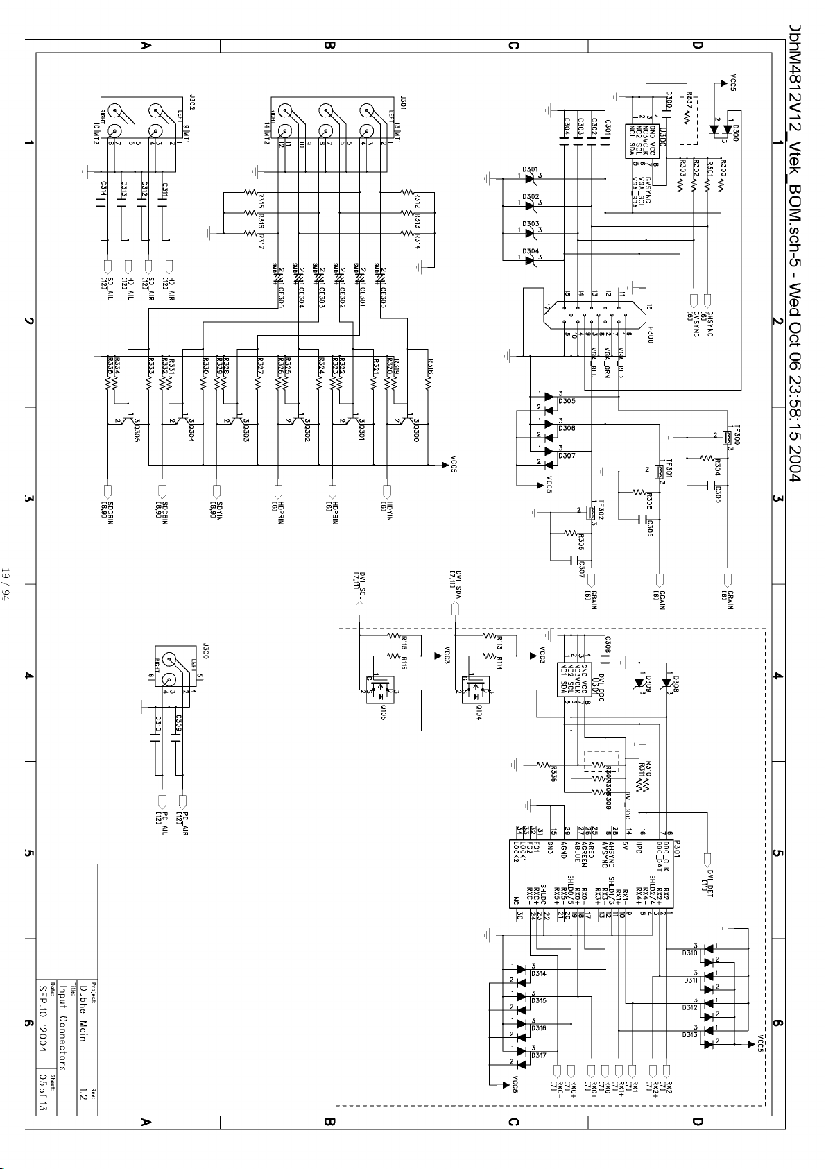
3bhM4812V12 Vtek BOM.sch-5 - Wed Oct 06 23:58:15 2004
19 / 94
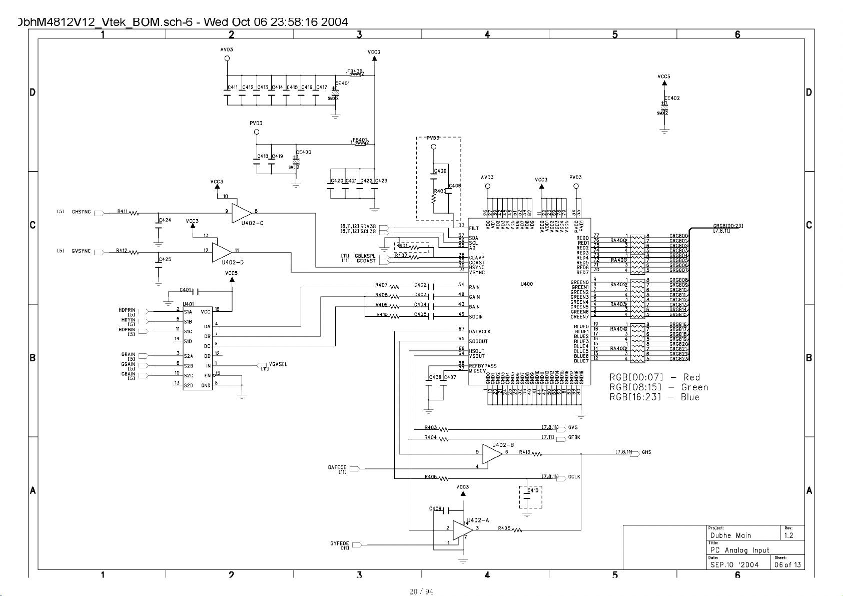
DbhM4812V12 Vtek BOM .sch-6 - Wed Oct 06 23:58:16 2004
O j
C411 jc^412_jc413_jc414Jc 415 Jc416 Jc 417 +
TTTTTT“M
PV
03
c
p
Ç41BjÇ419 +iï
CE400
:E401
?
2
1
■— 1—
JÇ420JÇ421JÇ422
io ^ T T T 1
[5] GHSYNC
Jc42
I
[5] GVSYNC
HDPRIN I
HDYIN I
HDPBIN I
GRAIN I--y_
GGAIN I--s_
[5] '
[5] '
[5] '
[5] '--^
rm 1
----
^
Jc42
I
__
— U401
2
S1A VCC
SIR
SIC
sin
S2A DD
S2B IN
S2C ËN
S2D GND
H \~
DA
DB
DC
VCC5
A
«FB40Q,
[8.11.12] SDA3G I
[8.11.12] 5CL3G
[11]
[11]
R40B w
K4P9 w
R41P w
----
----
----
-PV&3
C403| |
C404 | |
C405 | |
jc408_Jc4l
-----
Q
R40CT"
|
------
------
------
------
;
C4Q0
o
o it cm ro m to r- oo oi orrcMr'wm oz;
SDA REDO
SCL RED1
A0 RED2
CLAMP
COAST RED5
HSYNC RED6
VSYNC RED7
§+-
RAIN
4L
GAIN
43.
BAIN
49.
50GIN
AVD3
VCC3
A
ld in in to ^
U400 GREEN0
DATACLK
S0G0UT
HS0UT
VS0UT BLUE6
REFBYPASS
M!DSCV0
ÛQÛQÛQQÛQÛQÛÛQQÛQQQÛ
zzzzzzzzzzzzzzzzzzzz
CJ UU UUU UU UUU UU UCD UU UU U
PVD3
Q
RED3
RED4
GREEN1
GREEN2
GREEN3
GREEN4
GREEN5
GREEN6
GREEN7
BLUE0
BLUE1
BLUE2
BLUE3
BLUE4
BLUE5
BLUE7
VCC5
A
7fi RA40©
/h 3
74
73 1 -
RA4019
r?
71 3
/O
9 1 r
RA40Z>
K
/
6
5 1 -
4 RA403>
A
?
19 1 r
1H RA404?
17
IK
15 1 h
14 RA40®
13 3
12
4
4
3
4
3
4
3
4
4
B
fi
8
6 RRRROft
5
1R
7
fi
5 GRGR11,
8 BRRR19,
7 GRGB13/
fi
5
18
6
18
6 GRGR7Z
fi
RGB[00:07] - Red
RGB[08:15] - Green
RGB[16:23] - Blue
GRGB0L
GRGR07.
GRGB0.1
GRGR04
RRRROfi
GRGR07,
GRGBOa
RRRROft
RRRR10/
RRRR14/
GRGR15/
GRGR16/
RRRR17/
GRGR1B/
RRRR19,
GRGR7C1
RRRR71/
GRGB23
GRGBrOD:231
20/ 94
^402-A
3
-----
7
U4D2-B
6
---
R4Q5 VNAr~
Elli-wV-
JC4
[7.8.11|3—> GVS
[7.11] |--> GFBK
[7.6.1^ GHS
Project:
Dubhe Main
Title:
PC Analog Input
Date: Sheet:
Rev:
1.2
SEP.10 '2004 06 of 13
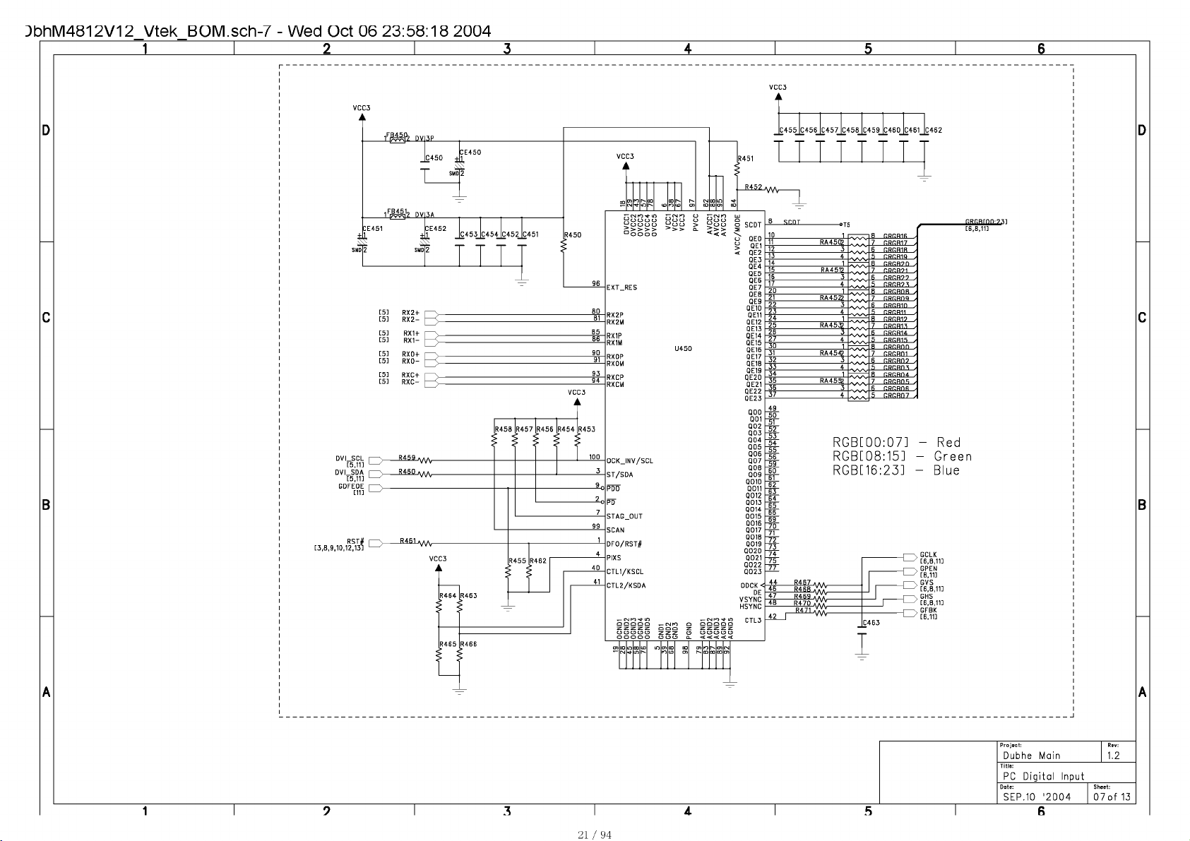
DbhM4812V12 Vtek BOM .sch-7 - Wed Oct 06 23:58:18 2004
JL
RX2+ I--v_
RX2- |—p
[5]
RX1 + I—v_
[5]
RX1- h^C
RX0+
RX0-
RXC+
R-
RXC-
DVLSCL I—>
DVLSDA I—. R460 » a a
GDFEOE I--\
[3,B,9,10,12,13J '--7 vv^
---
[5.11] '—7 vvv^
[5.11] '—7 vvv^
[11] '--^
RST# i-^
R459 VW-
______
---
VCC3
A
R458 R457 [R456 R454 R453
RX2P
RX2M
RX1P
RX1M
RXOP
RXOM
RXCP
RXCM
OCKJNV/SCL
ST/SDA
PDÜ"
PD
STAG_0UT
SCAN
DFO/RST#
PIXS
CTL1/KSCL
CTL2/KSDA
VCC3
A
C4SsJç*SS_£45’j:+SeJçJS9jç460_Ë+SlJç'
TTTTTTT
10 1 r
QEO
11 RA4503
QE1
12 3
QE2
13
QE3
14 1
QE4
15 RA4519
QE5
16 3
QE6
17
QE7
20 1
QE8
21 RA457?
QE9
22 3
0 E10
23
QE11
24 1
Q E12
25 RA453?
QE13
26
QE14
27
QE15
30 1
QE16
31
QE17
32 3
QE18
33
QE19
34 1
QE20
35
0E21
36 3
QE22
37
QE23
49
50
51
4
4
4
3
4
RA4549
4
RA45S
4
RGB[00:07]
RGB[08:15]
RGB[16:23]
7
7
7
8
7
R
P
7
R
7
5
RRRRH1
RRRRH5
RRRR07
Red
Green
Blue
21/ 94
O Q OQ Q
Project:
Dubhe Main
Title:
PC Digital Input
Date: Sheet:
Rev:
1.2
SEP.10 '2004 07 of 13
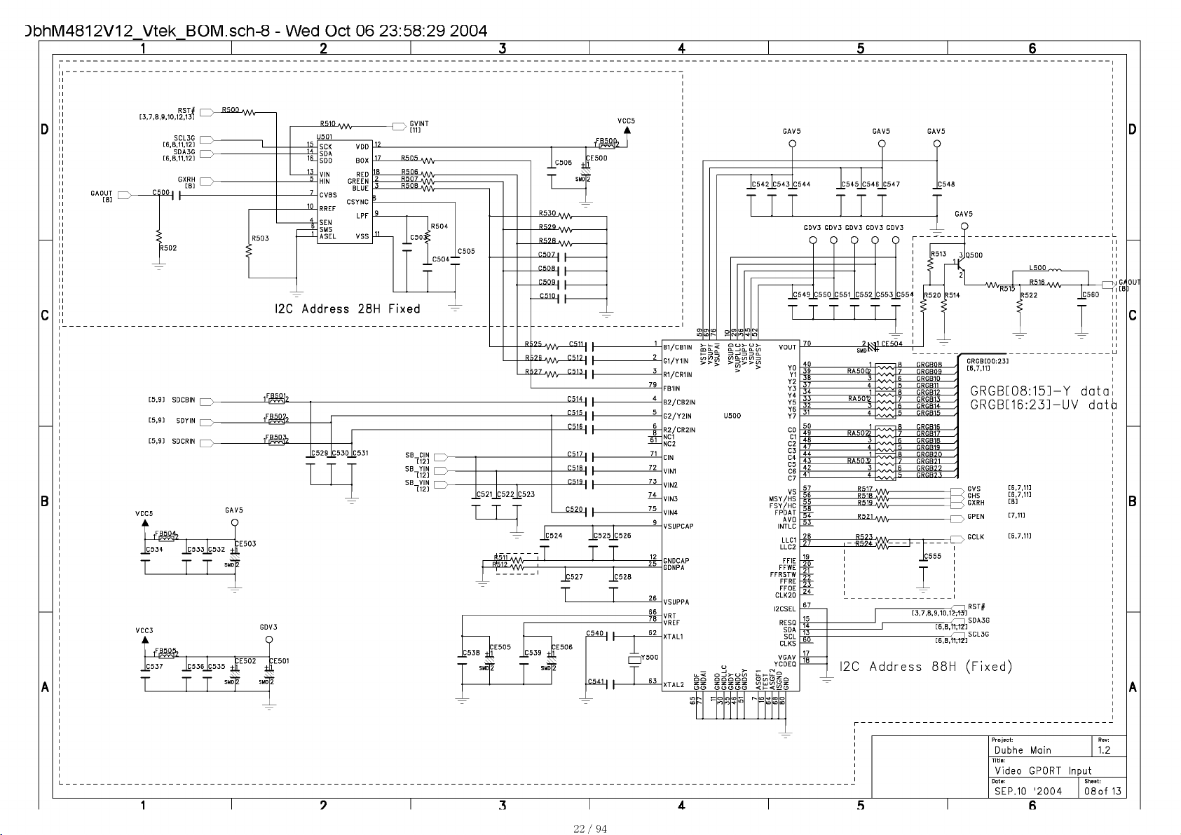
DbhM4812V12 Vtek BOM .sch-8 - Wed Oct 06 23:58:29 2004
22/ 94
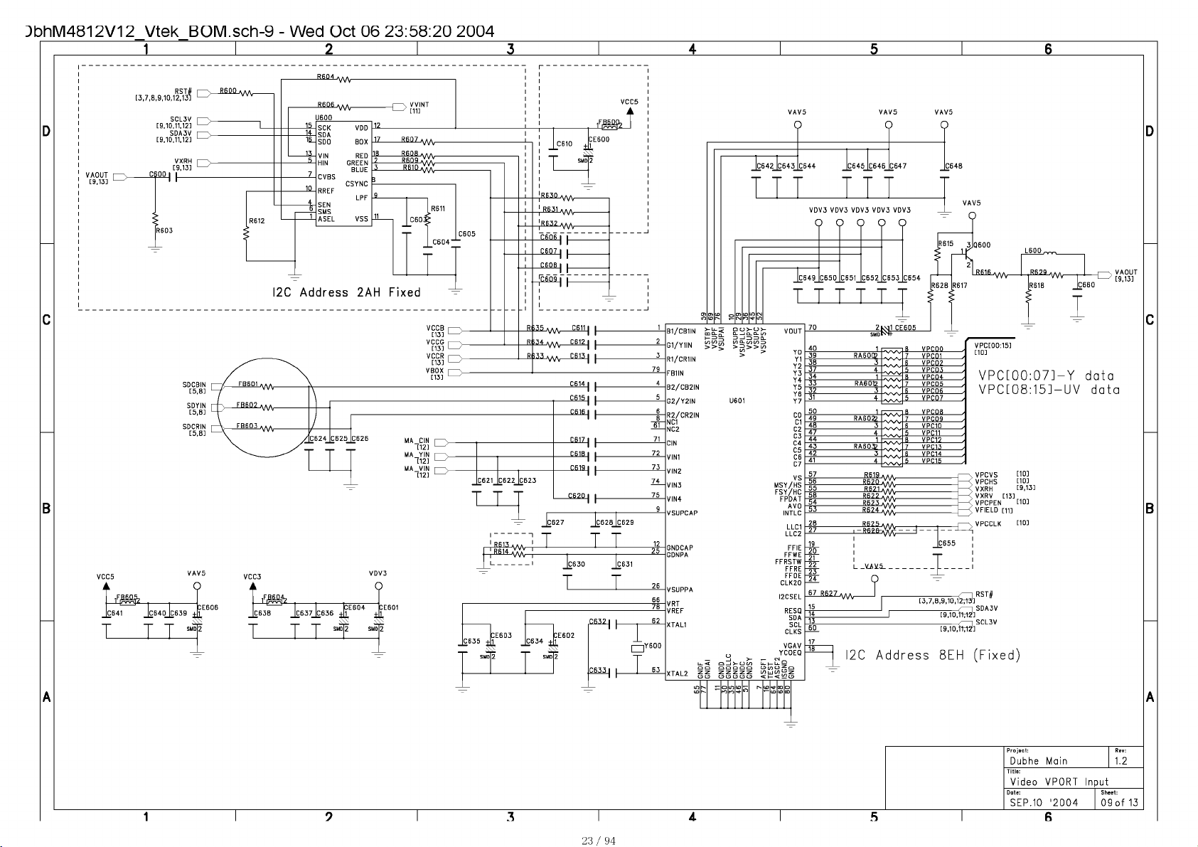
DbhM4812V12 Vtek BOM .sch-9 - Wed Oct 06 23:58:20 2004
23/ 94
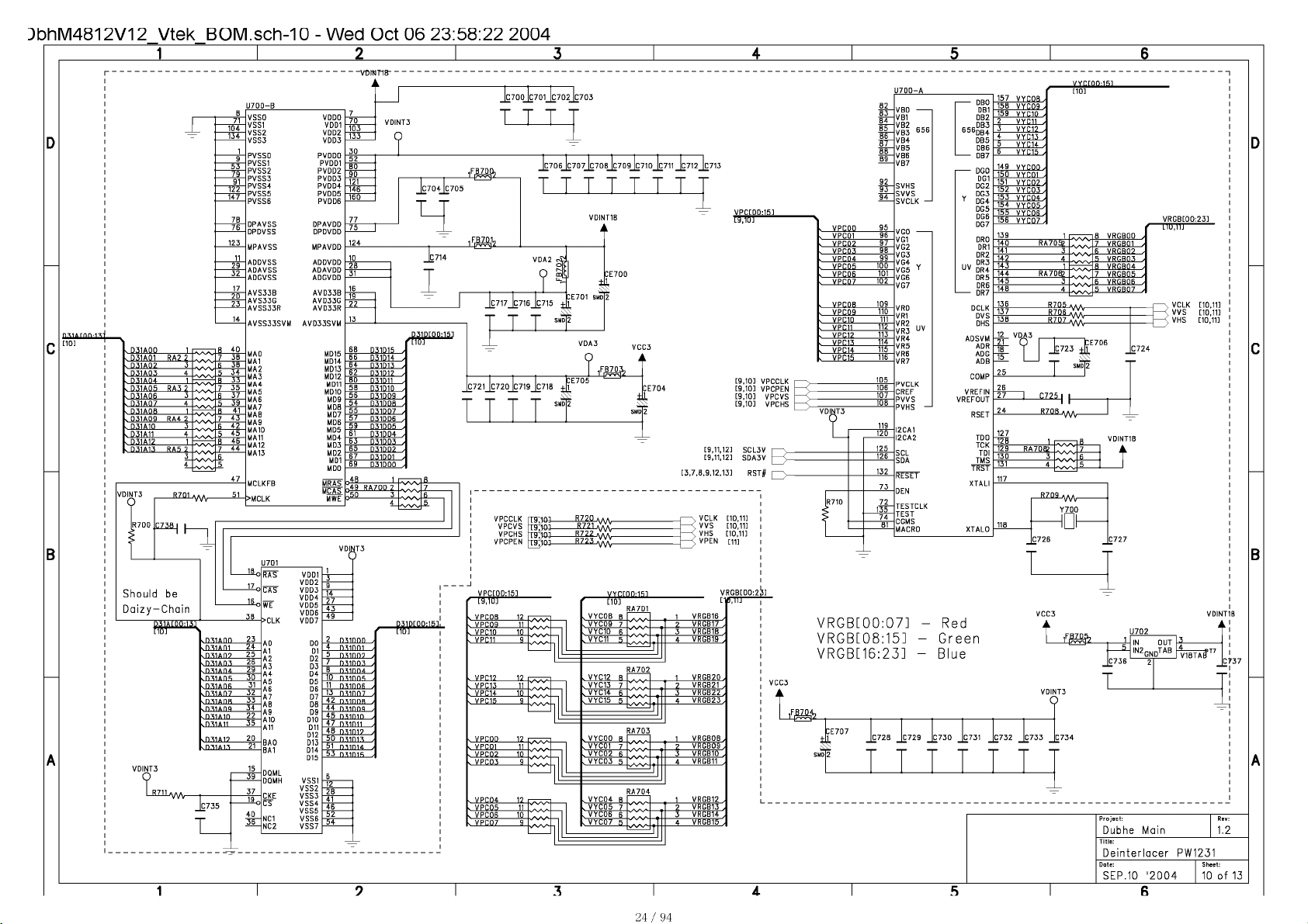
DbhM4812V12 Vtek BOM.sch-10 - Wed Oct 06 23:58:22 2004
„ D31A01 RA? ?
„ 031A07
, D31A03 4
< D31A04 1
, D31A05 RA3 ?
„ 031A06
< D31AQ7 4
. D31A0B 1
„ 031A09
RA4 2
, D31A10
, D31A11 4
. D31A12 1
V D31A13 RA5 2
0 C75B|
Should be
Daizy-Chain
3
3
3
'
C735
r
VSSO VDDO
_
71
VSS1 VDD1
104
VSS2 VDD2
134
VSS3 VDD3
PVSSO PVDDO
PVSS1 PVDD1
PVSS2 PVDD2
PVSS3 PVDD3
PVSS4 PVDD4
122
PVSS5 PVDD5
147
PVSS6 PVDD6
7B
DPAVSS DPAVDD
76
DPDVSS DPDVDD
123
MPAVSS MPAVDD
ADDVSS ADDVDD
ADAVSS ADAVDD
ADGVSS ADGVDD
AVS33B AVD33B
AVS55G AVD35G
AVSS33R AVD33R
AVSS33SVM AVD53SVM
£_40
MAO MD15
3B
7
MA1 MD14
3H
fi
MA2 MD13
5A4
MA3 MD12
33
R
MA4 MD11
35
7
MA5 MD10
3/
fi
MAß MD9
34
5
MA7 MDB
41
R
MAB MD7
43
7
MA9 MD6
41»
fi
MA1Û MD5
45
5
M A11 MD4
4h
R
MA12 MD3
44
7
MA15 MD2
MCLKFB MRÄS"
>MCLK UWE
osiaoo 25
24
22
35
20
21
15
39
37
13n
40
36
RAS VDD1
VDD2
CAS VDD3
VDD4
WE VDD5
VDD6
>CLK VDD7
AO DO
AI DI
A2 D2
A3 D3
A4 D4
A5 D5
A6 D6
A7 D7
AB DB
A9 D9
A10 D10
D11
All
D12
BAO D13
BA1 D14
D15
DQML
DQMH VSS1
VSS2
CKE VSS5
CS VSS4
VSS5
NC1 VSS6
NC2 VSS7
121
146
160
68 D51D15
66
H4
ßV D31D1?
Bl>
5B
hh 031009
54 D31D0R
55
5/
h»
61
53
Rh 03100?
67
MD1
t>y
MDO
MCAS
V DINT 3
2 osioon
4
5
/
H
11)
11
13
4/1
44
4 h
4/
4H
.40
51
53
031015
--V0tNT18--
Á
D31D14
031013
D31D11
D31D10
D31D07
D31DD6
031005
D31D04
031003
D31D01
D51D00
,
,
,
,
,
,
,
,
,
,
,
,
,
,
,
,
,
,
,
,
,
,
,
,
,
■W“
lFB70a,
Jc704_]c705
_Jc 71
I
C721_[c720_|c719_|c71B -J?E7°5
T T T T 1
’ L9.1ÜJ
. vpnnR 1?
„ VPC09
, VPC10
. VPC11
„ VPC15
. VPC14
„ VPC15
, VPC01
. VPC02
, VPC03
. VPC05
. VPCOR
„ VPC07
Je 7 0 oje 7 01_Jc 7 02_Jc 71
T T T
jç706_jç707jç708jç709_jç710_lç711 Jç712_[c7'
T T T T T T T
JÇ717_|Ç716_|Ç715
T T
VPCCLK
[TOM
VPCVS
VPCHS
VPCPEN
VPC[0D:15]
11
10
9
11
10
9
11
10
9
11
10
W SA —i
9
V W 1
VDINT18
A
:e700
VDA3
VCC3
A
îfl
CE704
s
SMD 2
R720
--
R721
R722
R725
' [10]
RA7D1
.VYCOB B
. VYC09 7
. VYC10 R 5 VRGB18 .
. VYC11 5 4 VRGB19 .
RA702
. VYC12 R
. VYC13 7 ? VRGB21 .
✓W'
. VYC14 fi
. VYC15 ñ 4 VRGB25.
RA703
. VYCOO R
. VYC01 7 ? VRGB09.
./W"
. VYC02 fi
. VYC03 ñ 4 VRGB11 .
VYC04 B 1 VRGB12
VYC06 6
VYC07 R
[9.11.12]
[9.11.12]
[5,7,8,9,12,13] RST# |
1 VRGB16 .
? VRGB17 .
I
1 VRGB20.
3 VRGB22.
I
1 VRGBOB.
3 VRGB10 .
I
VPCC00:15]
mn
[9.10] VPCCLK
[9.10] VPCPEN
[9.10] VPCVS
[9.10] VPCHS
SCL3V
SDA3V
L
----
92
93
94
V VPCOO
. VPC01
» VPCO?
. VPC03
V VPC04
. vpnoñ
V VPC06
„ VPC07
V VPCOB
. VPC09
V VPC10
„ VPC11
» VPC1?
» VPH13
, VPC14
, VPC15
95
96
97
98
99
100
101
102
109
110
111
112
113
114
115
116
-->_
72
135
VRGB[00:07] - Red
VRGB[08:15] - Green
VRGB[16:23] - Blue
Jç72B Jç729 jc730 jç731 jç732 jç735 C;
T T T T T T
VBO
VB1
VB2
VB3
VB4
VB5
VB6
VB7
SVHS
SWS
SVCLK —1
VGO
VG1
VG2
VG3
VG4
VG5
VG6
VG7
VRO
VR1
VR2
VR3
VR4
VR5
VR6
VR7
PVCLK
CREF
PWS
PVHS •
I2CA1
I2CA2
SCL
SDA
DEN
TESTCLK
TEST
CGMS
MACRO
— DB0
DB1
DB2
R*RDB3
bSt»DB4
DB5
DB6
— DB7
— DG0
DG1
DG2
V DG5
Y DG4
DG5
DG6
DG7
DR2
. DR3
' DR4
DR5
DR6
- DR7
DCLK
DVS
DHS
ADSVM
ADR
ADG
ADB
COMP
VREFIN
VREFOUT
TDO
TCK
TDI
TMS
TRST
XTALI
157
VYCOR ,
15B
VYC09/
15»
VYC10 ,
V
VYC11 ,
3
VYC1? ,
4
VYC13 .
5
VYC14 ,
H
VYC15 ,
149
VYCOO/
1S0
VYCm ,
151
VYCO?,
152
VYR03 ,
153
VYC04/
154
VYC05/
155
VYC06/
15b
VYC07/
140 RA705P
141 3
142
143 1 -
144 RA708?
145 3
14B
12 VDA3
21
18
fj ^723 ff
I smd|2
27 J C725
129 RA70R?
130 3
131
R708 a
4
“AVr
\ h
Y700
HDh
L
_£gg£_
VDINT3
o
VYcroo:i5i
RVRßROO ,
VRRR01 .
VRßRO? ,
4
VRGB03 /
5
VRGR04 ,
fi
VRGR05 .
7
VRßROfi ,
4
VRGB07 ,
5
I.
Project:
Dubhe Main
Title:
Deinterlacer PW1231
Date: Sheet:
SEP.10 '2004 10 Of 13
VRGB[00:23]
LID,TU
----------
> VCLK [10,11]
> WS [10,11]
V VHS [10,11]
OUT
mTAB
VDINT1
A
Rev:
1.2
24/94
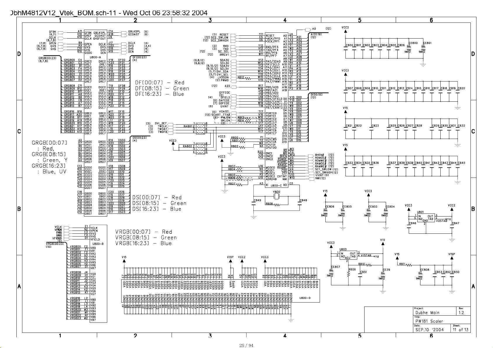
DbhM4812V12 Vtek BOM.sch-11 - Wed Oct 06 23:58:32 2004
GFBK i
[6,7] 1
GCLK i
[6,7,8] 1
[7,8] GPEN I
[6.7.8] GVS
[6.7.8] GHS
GRGB[00:23]
[6,7,B]
. GRGB01
. GRGR07 M
. GRGB03 h 4
. GRGBÛ4 U2
. GRGB05 U
. GRGB06 DA
. GRGB07 \)V
. GRGB08 C11
. GRGBÛ9Ü12
. GRGB10 Hl 1
. GRGB11 AH
. GRGB12 HK
. GRGB13 V.H
. GRGB14 A/
. GRGB15 H/
. GRGB16 R1R
. GRGB17A/’t)
. GRGB18 Hl/
. GRGB19 A19
. GRGB20Hl K
. GRGB21A1 /
. GRGB22
. GRGB23A1 b
GRGB[00:07]
: Red,
GRGB[08:15]
: Green, Y
GRGB[16:23]
: Blue, UV
VCLK
vrcs
VW3
vm
VFIBCD
_tai
VRGB[00:23]
[10]
GRGBQO E4
CA
A1h
C15
B15
A14
B14
A13
C12
B13
A12
VRGBOO E2
. VRGB01
. VRGB02
. VRGB03
. VRGB04
. VRGB05 HA
. VRGB06 HV
. VRGB07
. VRGB08
. VRGB09
. VRGB10 JA
. VRGB11
. VRGB12
. VRGB13 KA
. VRGB14 KV
. VRGB15 Kl
. VRGB6 1 ?
. VRGB/ 1 1
. VRGBHI A
. VRGB9 L4
. VRGB2DMA
. VRGB21 M1
. VRGB22
. VRGB23 M2
GFBKGBLKSPL
GREFGCOAST
GCLKGHSFOUT
GPEN DCLK
(WS
DVS
GHS DHS
USOG DEN
U800-A
GREO DREO
GRM DREI
GRE2 DRE2
GRE3 DRE3
GRE4 DRE4
GRE5 DRE5
GRE6 DRE6
GRE7 DRE7
GGEO DGEO
GGE1 DGE1
GGE2 DGE2
GGE3 DGE3
GGE4 DGE4
GGE5 DGE5
GGE6 DGE6
GGE7 DGE7
GBEO DBEO
GBE1 DBE1
GBE2 DBE2
GBE3 DBE3
GBE4 DBE4
GBE5 DBE5
GBE6 DBE6
GBE7 DBE7
GROO DROO
GR01 DR01
GR02 DR02
GROA
DR03
GR04 DR04
GR05 DR05
GR06 DR06
GR07 DR07
GGOO DGOO
GG01 DG01
GG02 DG02
GG03 DG03
GG04 DG04
GG05 DG05
GG06 DG06
GG07 DG07
GBOO DBOO
GB01 DB01
GB02 DB02
GB03 DB03
GH04 DB04
GB05 DB05
GB06 DB06
GB07 DB07
VCLK
VPEN
WS
VHS
VFIELD
VRO
H
VR1
\'i
VR2
UA
VR3
li?
VR4
VR5
VR6
1,1
VR7
,14
VGO
Hl
VG1
VG2
Ji»
VG3
J1
VG4
VG5
VG6
VG7
VBO
VB1
VB2
VB3
VB4
VB5
NI
VB6
VB7
A18 I—< GCOAST [6]
Y20 DFD1
R16 DF02
U19 DFD3
RIB
W20 DFD5
V20 DFD6
U20 DFD7
T19 DF08
T2Q DFD9
R19 DF1D
R20 DF11
M18 DF12
P18 DF13
P19 DF14
P20 DF15
M17 DF16
N20 DF17
M20 DF18
L17 DF19
M19 DF20
K17 DF21
L19 DF22
L20 DF23
K19 DSOO
K20 DS01
K1B DS02
J20 DS03
J18 DS04
J19 DS05
H20 DS06
H19 DS07
H18 DSOB
H17 DS09
G20 DS10
G19 DS11
G18 DS12
F20 DS13
F19 DS14
F18 DS15
E20 DS16
E19 DS17
E18 DS18
F17 DS19
D20 DS2D
D19 DS21
D16 DS22
D17 DS23
GBLKSPL [6]
[3,4]
[4]
[4]
DF[00:23]
[4] [6,8,12]
,
,
DF04
,
,
DF[00:07]
,
DF[08:15]
,
,
DF[16:23]
,
,
,
,
,
,
,
,
[5] DVI_DET
,
,
,
,
,
,
,
,
,
,
,
,
,
,
,
,
,
,
,
,
,
[3] TWCLK
[3] TWDAT
[3] TWDFB
DS[00:23]
[4]
DS[00:07]
DS[08:15]
DS[16:23]
[6,8,12]
Red
Sreen
Blue
Red
Green
Blue
VRGB[00:07] - Red
VRGB[08:15] - Green
VRGB[16:23] - Blue
V15
Á
io io ifs in io
9999q9o2S2d2Sd2c
¿Ü Ü ÛD Q ÜQ Û
-CNKWWtOr-OOO
Û ÛÛ Û Û Û QÛ Û Û Q ÛÛ Û Q ÛÛ Û Û ÛÛ Û Û ÛÛ Û Û ÛÛ Û Û ÛÛ Û Û ÛQ Û
z z z z z z z z z z z z z z z z z z z z z z z z z z z z z z z z z z z z z z
> > > > > > > > > '
MCMtMCNCMCNCMC'JC'
RESET
[12] SC2_SWL0W
[12] SC2_SWHIGH
Q Q Q Q
QÛ Û Q
>>>>
a œ i i
SMD|2 SMD 2
TTTTTTT
CBO7_[cB0bJcBO9_[cB1O_1cB11 _jcß12_]c 813_jcß14_}c B15_]c816_lc817_]cB1ß_lc819 Jcj
TTTTTTTTTTTTT
CB2ijçB22 jcB23 jçS25_lçB26_jçS27_[çBZe _jç829_jç83ojç831 jçj
TT T TTTT TTT
C B3^jcB3 ^jc B35_jc B36 jcß37_lc B3ßjcß39_[c B4 q_lcB41_[cB42_lcB43_[c844jcj
TTTT TTTTTTTT
VCC3
▲
OUT
,.|TAB
R.B10
Jç8!
1
)EB03 CE804
VCC3
A
L.
Project:
Dubhe Main
Title:
PW181 Scaler
Date: Sheet:
SEP.10 '2004 11 of 13
WB™
jçB53_jçB52 CI
11
VCC2
À
V15P
Á
Rev:
1.2
25/94
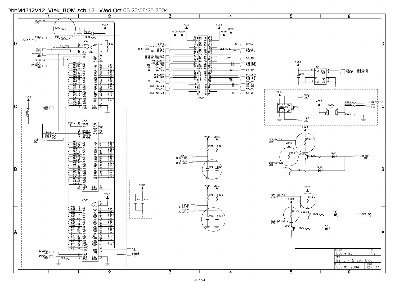
DbhM4812V12 Vtek BOM.sch-12 - Wed Oct 06 23:58:25 2004
RST# I
[3,7,8,9,10,12,13] 1—
-----
VCC3
A
VCC5 VAMP
>
RSTj
[3,7,8,9,10,12,13]
[6,8,11,12] SDA3G |
[2] REG5A I
[9,10,11,12BDA3V
[9,10,11,12]SCL3V
[13] SC1_B0X
[13] SC1_GRN
[12] SC1_SW
[9] MA_VIN
[9] MA_CIN
SC2_BLU I
SC2_RED
[5] S D_AIR I
[5] SD_AIL I
A A
SDA3G
[6,8,11,12]
SCL3G I
re b 11 ion 1--/
49
4/ 4H
4h
4 A44
41
AW41)
At
Ah
AAA4
A1
y 9
vt VH
Vh VH
VA
?1 VV
1«
1/ 1K
1h
1A 14
11 VV
9
/
h 6
A
1 2
-----
V
VCC3
50
46
4 y
AK
AH
AV
At)
V 4
VO
16
10
K
4
VCC3 VCC3
A
_<--1 REGBV
SCL3G
PWR33V
«
l SC1_BLU
I SC1_RED
] MA_YIN
SC2_B0X
SC2_GRN
SC2_SW
SB_V IN
SB_CIN
HD_AIR
HD_AIL
1 SCL3G [6,8,11,12]
SDA3G [6,8,11,12]
1 P C_AIL
R904 a « * I
-----
x IRRCVh [
SBi-pWLOW
SEi-pWHIGl
6
001 .
9
007 .
11)
003 .
13
D04 ,
14
005 .
15
D06 ,
IK 007 .
?9
D08 ,
Al>
009 .
31
D10 ,
AV
011 .
Ah
01? .
AH
013 .
At 014 .
AH
D15 >
39
40 h
1?
A4
1
-----
1
- 1
ptS:
Ï
ta
26/ 94
Se^SWLOW
SE^SWHIGI
Project:
Dubhe Main
Title:
Memory & Etc. Block
Date: Sheet:
Rev:
1.2
SEP.10 '2004 12 of 13
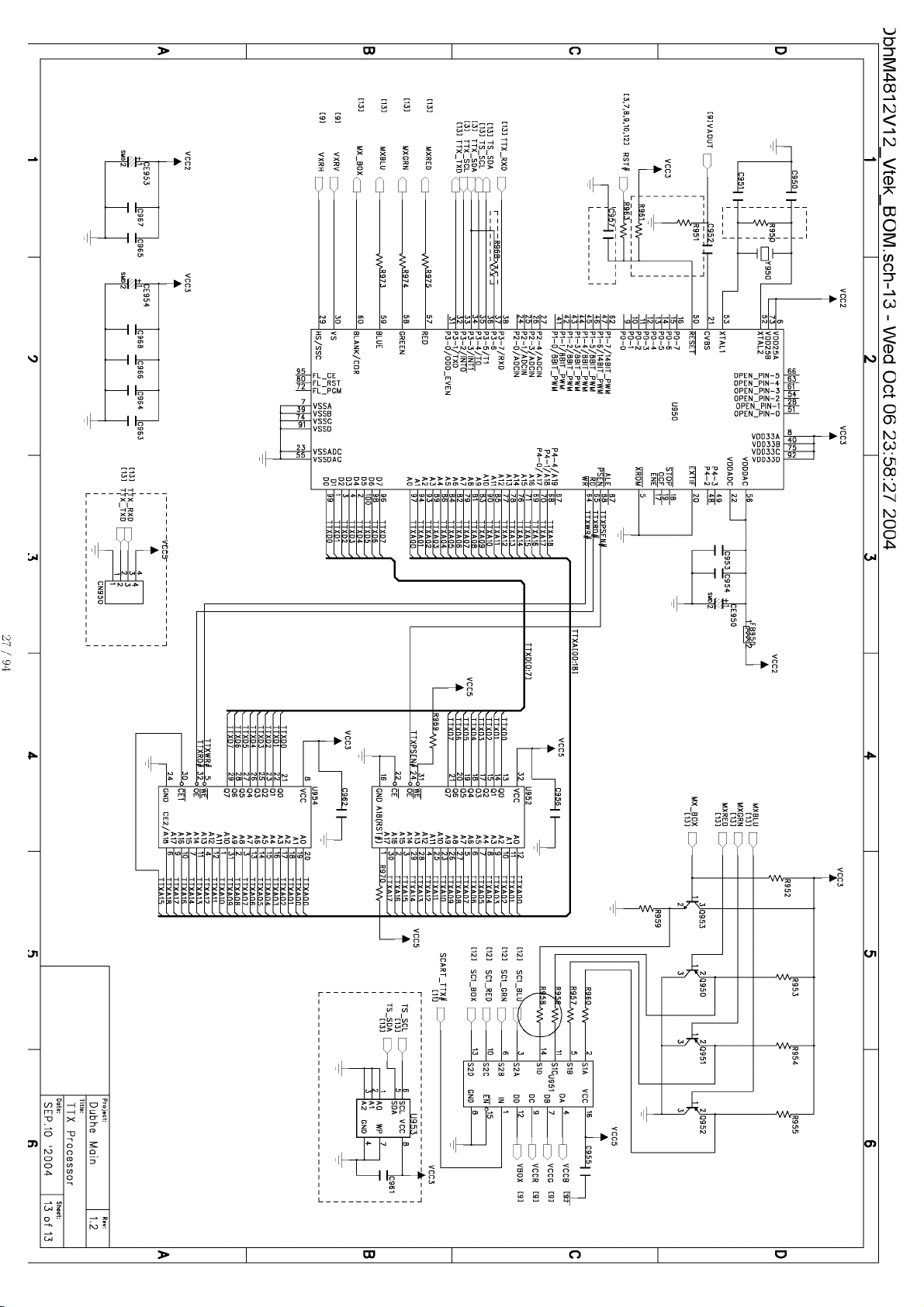
3bhM4812V12 Vtek BOM.sch-13 - Wed Oct 06 23:58:27 2004
27 /9 4
 Loading...