

Page 1

SERVICE MANUAL
Model:
LCT-4216
Safety Precaution
Technical Specifications
Block Diagram
Circuit Diagram
Basic Operations & Circuit Description
Main IC Specifications
Product Specification of POWER board
Product Specification of LCD Module
Exploded View
Spare parts list
If you forget your V-Chip Password
Software Upgrade
This manual is the latest at the time of printing, and does not
include the modification which may be made after the printing,
by the constant improvement of product.
Page 2
Safety Precaution
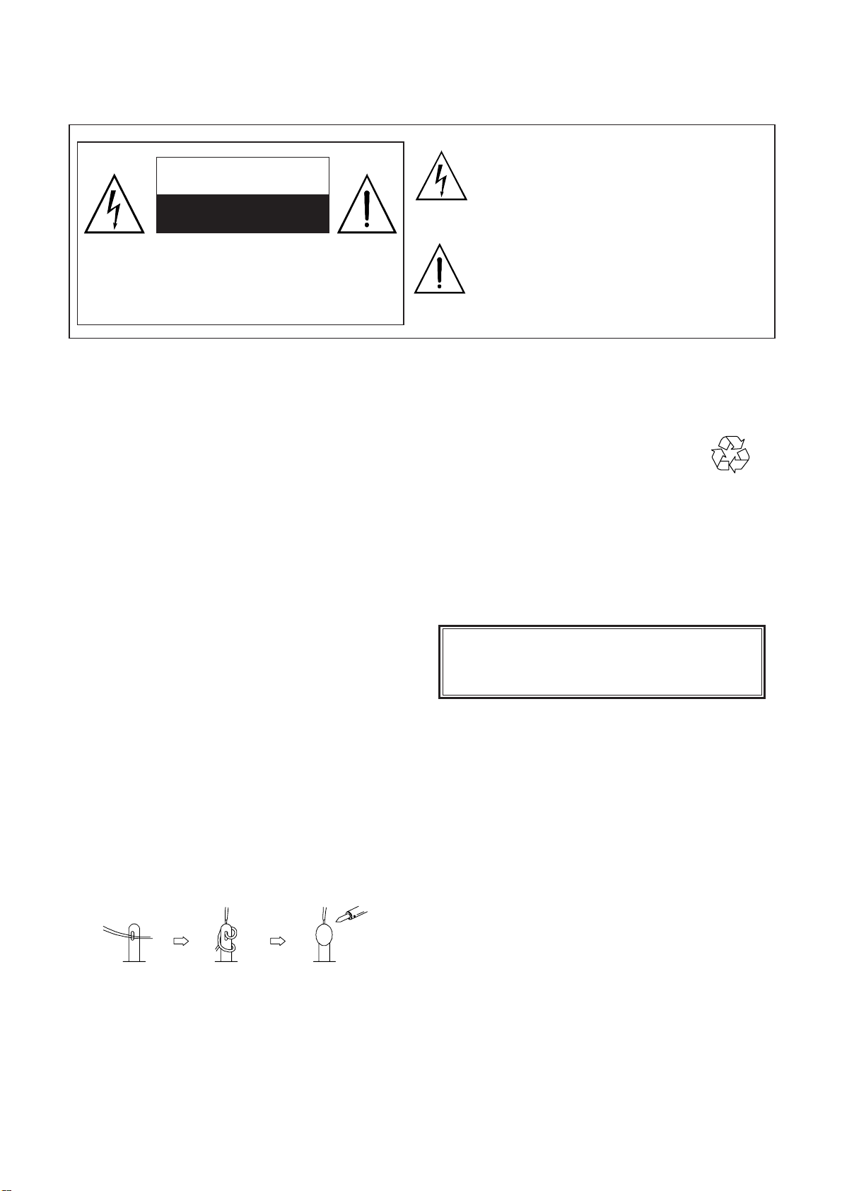
CAUTION
RISK OF ELECTRIC SHOCK
DO NOT OPEN
The lightning flash with arrowhead symbol,
within an equilateral triangle, is intended to
alert the user to the presence of uninsulated
“dangerous voltage” within the product’s enclo
sure that may be of sufficient magnitude to
constitute a risk of electric shock to persons.
CAUTION: TO REDUCE THE RISK OF
ELECTRIC SHOCK, DO NOT REMOVE COVER
(OR BACK). NO USER-SERVICEABLE PARTS
INSIDE. REFER SERVICING TO QUALIFIED
SERVICE PERSONNEL ONLY.
PRECAUTIONS DURING
SERVICING
1. In addition to safety, other parts and
assemblies are specified for conformance with
such regulations as those applying to spurious
radiation. These must also be replaced only
with specified replacements.
Examples: RF converters, tuner units, antenna
selection switches, RF cables, noise-blocking
capacitors, noise-blocking filters, etc.
2. Use specified internal Wiring. Note especially:
1) Wires covered with PVC tubing
2) Double insulated wires
3) High voltage leads
3. Use specified insulating materials for hazardous
live parts. Note especially:
1) Insulating Tape
2) PVC tubing
3) Spacers (insulating barriers)
4) Insulating sheets for transistors
5) Plastic screws for fixing micro switches
4. When replacing AC primary side components
(transformers, power cords, noise blocking
capacitors, etc.), wrap ends of wires securely
about the terminals before soldering.
5. Make sure that wires do not contact heat
generating parts (heat sinks, oxide metal film
resistors, fusible resistors, etc.)
6. Check if replaced wires do not contact sharply
edged or pointed parts.
7. Make sure that foreign objects (screws, solder
droplets, etc.) do not remain inside the set.
The exclamation point within an equilateral
triangle is intended to alert the user to the
presence of important operating and
maintenance (servicing) instructions in the
literature accompanying the appliance.
MAKE YOUR CONTRIBUTION
TO PROTECT THE
ENVIRONMENT
Used batteries with the ISO symbol
for recycling as well as small accumulators
(rechargeable batteries), mini-batteries (cells) and
starter batteries should not be thrown into the
garbage can.
Please leave them at an appropriate depot.
WARNING:
Before servicing this TV receiver, read the
SAFETY INSTRUCTION and PRODUCT
SAFETY NOTICE.
SAFETY INSTRUCTION
The service should not be attempted by anyone
unfamiliar with the necessary instructions on this
apparatus. The following are the necessary
instructions to be observed before servicing.
1. An isolation transformer should be connected in
the power line between the receiver and the
AC line when a service is performed on the
primary of the converter transformer of the set.
2. Comply with all caution and safety related
provided on the back of the cabinet, inside the
cabinet, on the chassis or picture tube.
3. To avoid a shock hazard, always discharge the
picture tube's anode to the chassis ground
before removing the anode cap.
4. Completely discharge the high potential voltage
of the picture tube before handling. The picture
tube is a vacuum and if broken, the glass will
explode.
Page 3

5. When replacing a MAIN PCB in the cabinet,
always be certain that all protective are
installed properly such as control knobs,
adjustment covers or shields, barriers, isolation
resistor networks etc.
6. When servicing is required, observe the original
lead dressing. Extra precaution should be given
to assure correct lead dressing in the high
voltage area.
7. Keep wires away from high voltage or high
tempera ture components.
8. Before returning the set to the customer,
always perform an AC leakage current check
on the exposed metallic parts of the cabinet,
such as antennas, terminals, screwheads,metal
overlay, control shafts, etc., to be sure the set
is safe to operate without danger of electrical
shock. Plug the AC line cord directly to the
AC outlet (do not use a line isolation
transformer during this check). Use an AC
voltmeter having 5K ohms volt sensitivity or
more in the following manner.
Connect a 1.5K ohm 10 watt resistor paralleled
by a 0.15µF AC type capacitor, between a
good earth ground (water pipe, conductor etc.,)
and the exposed metallic parts, one at a time.
Measure the AC voltage across the combination
of the 1.5K ohm resistor and 0.15 uF
capacitor. Reverse the AC plug at the AC
outlet and repeat the AC voltage measurements
for each exposed metallic part.
The measured voltage must not exceed 0.3V
RMS.
This corresponds to 0.5mA AC. Any value
exceeding this limit constitutes a potential
shock hazard and must be corrected
immediately.
The resistance measurement should be done
between accessible exposed metal parts and
power cord plug prongs with the power switch
"ON". The resistance should be more than
6M ohms.
AC VOLTMETER
PRODUCT SAFETY NOTICE
Many electrical and mechanical parts in this
apparatus have special safety-related
characteristics.
These characteristics are offer passed
unnoticed by visual spection and the protection
afforded by them cannot necessarily be obtained
by using replacement components rates for a
higher voltage, wattage, etc.
The replacement parts which have these
special safety characteristics are identified by
marks on the schematic diagram and on the parts
list.
Before replacing any of these components,
read the parts list in this manual carefully. The
use of substitute replacement parts which do not
have the same safety characteristics as specified
in the parts list may create shock, fire, or other
hazards.
9. Must be sure that the ground wire of the AC
inlet is connected with the ground of the
apparatus properly.
Good earth ground
such as the water
pipe, conductor,
etc.
AC Leakage Current Check
Place this probe
on each exposed
metallic part
Page 4
Technical Specifications
MODEL : LCT-4216
42” LCD-TV
DATE FIRST ISSUED
ISSUE
RAISED BY
1
REVISIONS
ISSUED DATE DESCRIPTION RAISED BY :
CHECKED BY
NUMBER OF PAGES
9
SPECIFICATION AGREED : SIGNATURE DATE
R & D DEPARTMENT
COMMERCIAL DEPARTMENT
PRODUCTION DEPARTMENT
Q/A DEPARTMENT
CUSTOMER
SPECIFICATION APPROVED :
.
......................................................................................
......
......................................................................................
......
......................................................................................
.......
......................................................................................
.......
......................................................................................
.......
SIGNATURE :
...........................
...
...........................
...
...........................
...
...........................
...
...........................
...
DATE :
NOTE :
Only documents stamped “Controlled Document” to be used for manufacture of production parts.
Page 5
CONTINUATION PAGE
Technical Specifications
LCT-4216
NUMBER
2 OF 9 PAGES
1. Standard Test Conditions
All tests shall be performed under the following conditions, unless otherwise specified.
1.1 Ambient light
1.2 Viewing distance
1.3 Warm up time
1.4 PDP Panel facing
1.5 Measuring Equipment
: 150ux (When measuring IB, the ambient luminance
≦0.1Cd/m
2
)
: 50cm in front of LCD
: 30 minutes
: no restricted
: PC, Chroma 2225 signal generator (with Chroma digital
additional card) or equivalent, Minolta CA100 photometer
1.6 Magnetic field
1.7 Control settings
1.8 Power input
: no restricted
: Brightness, Contrast, Tint, Color set at Center(50)
: 100~240Vac
1.9 Ambient temperature : 20°C ± 5°C (68°F ± 9°F)
1.10 Display mode
: 31.5KHz/60Hz (Resolution 1366 x 768)
1.11 Other conditions
:
1.11.1 With image sticking protection of LCD module, the luminance will descend
by time on a same still screen and rapidly go down in 5 minutes. When
measuring the color tracking and luminance of a same still screen, be sure t
o accomplish the measurement in one minute to ensure its accuracy.
1.11.2 Due to the structure of LCD, the extra-high-bright same screen should not
hold over 5 minutes for fear of branding on the panel.
Page 6
Technical Specifications
ELECTRICAL CHARACTERISTICS
2. Power Input
LCT-4216
CONTINUATION PAGE
NUMBER
3 OF 9 PAGES
2.1 Voltage
2.2 Input Current
2.3 Maximum Inrush Current
: 100 ~ 240VAC
: 2.5 / 1.1A
: <30 A (FOR AC110V ONLY)
Test condition : Measured when switched off for at least 20 mins
2.4 Frequency
2.5 Power Consumption
: 50Hz to 60Hz(±3Hz)
: ≤250W
Test condition : full white display with maximum brightness and
contrast
2.6 Power Factor
2.7 Withstanding voltage
: Meets IEC1000-3-2
: 1.5kVac or 2.2kVdc for 1 sec
3. Display
3.1 Screen Size : 42” LCD
3.2 Aspect Ratio : 16:9
3.3 Pixel Resolution : 1366x768
3.4 Peak Brightness : 400 cd/m² (TYPE)
3.5 Contrast Ratio (Dark room) : 500:1 ( TYPE)
3.6 Viewing Angle : Over 176°
3.7 OSD language : English/Frensh/Spanish
4. Signal
4.1 AV & Graphic input
4.1.1 TV standard : NTSC
4.1.2 TV Tuning system : PLL 181Ch
4.1.3 CATV : 125CH
4.1.4 Composite signal : CVBS
4.1.5 Y,C Signal : S-Video
4.1.6 Component signal : Y, Pb/Cb, Pr/Cr, HDTV compatible
4.1.7 Graphic I/P : Analog: D-sub 15pin detachable cable
Digital: DVI
4.1.8 PnP compatibility : DDC 1.0
4.1.9 I/P frequency : f
: 31.5kHz to 60kHz/fV: 56.25Hz to 75Hz (1024x768
H
recommended)
Page 7
Technical Specifications
LCT-4216
4.2 Audio input
Audio I/P(L/Rx5) : 1 for DVI / D-Sub
1 for Y/ Pb/Pr
1 for Y/ Cb/Cr
1 for CVBS
1 for S-Video
4.3 Audio output
Audio/Video O/P(RCAx3) : Monitor out(L/R,CVBS),Subwoofer out
4.4 Other function
: PIP/POP/PBP, Zoom,Last Memory,User-friendly OSD menu
5. Environment
5.1 Operating environment
5.1.1 Temperature : 5º to 30°C
5.1.2 Relative humidity: 20% to 85%(non-condensing)
CONTINUATION PAGE
NUMBER
4 OF 9 PAGES
5.2 Storage and Transport
5.2.1 Temperature : -20°C to 60°C(-4º to 140°F)
5.2.2 Relative humidity: 5% to 95%
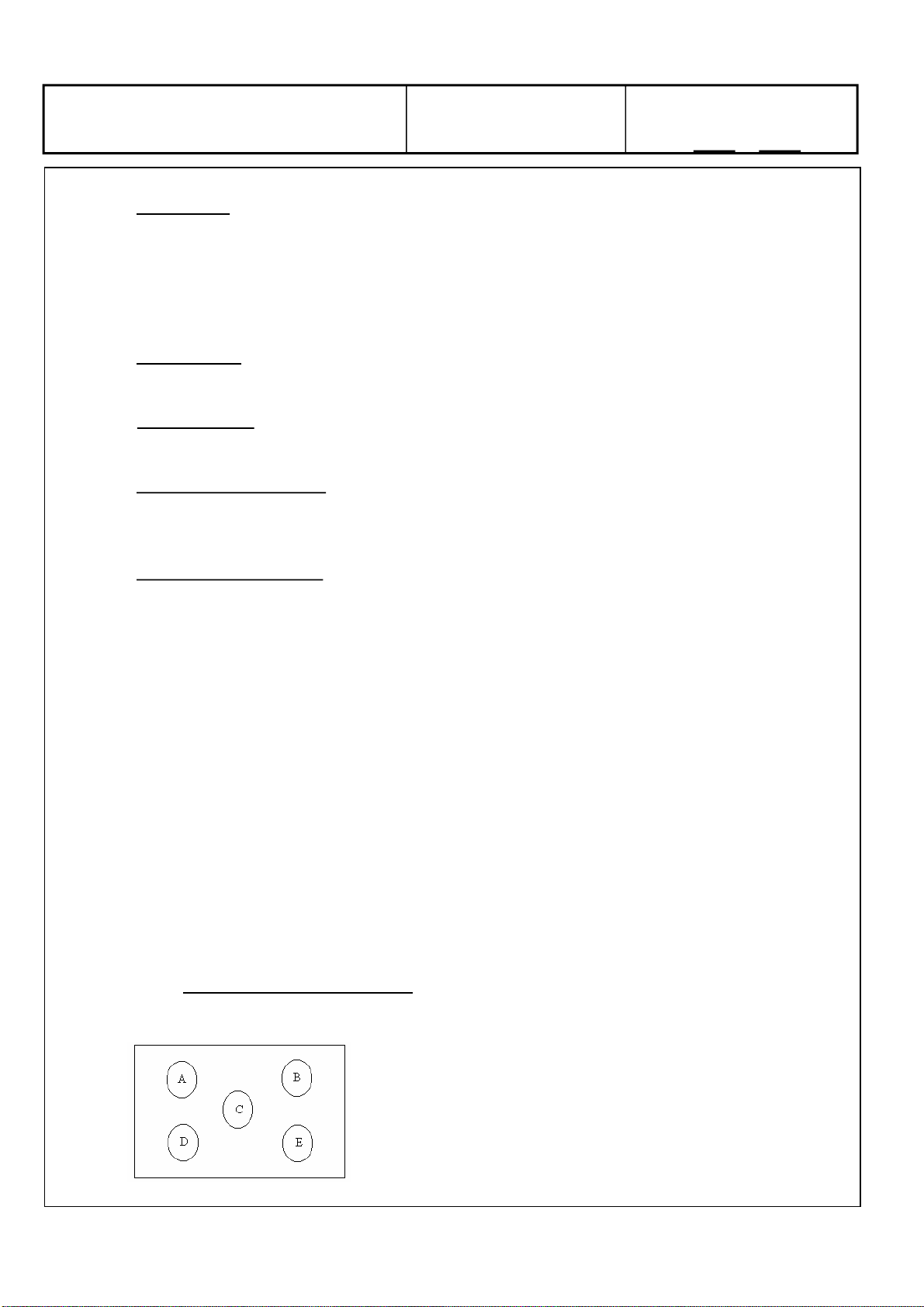
6. Panel Characteristics
6.1 Type : LG420W02
6.2 Size : 42.02inches diagonal,
1006mm(H)x610mm(V)x59mm(D)(TYPE)
6.3 Aspect ratio : 16:9
6.4 Viewing angle : Over 176°
6.5 Resolution : 1366X768
6.6 Weight : 14.8kg ±0.5 kg (Net)
6.7 Color : 16.77 million colors by combination of 8 bits R,G,B digital
6.8 Contrast : Typical 400:1
6.9 Peak brightness : Typical 500cd/ ㎡
6.10 Color Coordinate Uniformity
: Contrast; Brightness and Color control at normal
setting
Test Pattern : Full white pattern
Average of point A,B,C,D and E +/- 0.01
Page 8

Technical Specifications
LCT4216
CONTINUATION PAGE
NUMBER
5 OF 9 PAGES
6.11 Color temperature
: Contrast at center (50); Brightness center (50);
Color temperature set at Natural
x=0.295±0.02
y=0.300±0.02
6.12 Cell Defect Specifications
Subject to Panel supplier specification as appends.
7. Front Panel Control Button
7.1 CH Up / Down Button : Push the key to changing the channel up or down.
When selecting the item on OSD menu.
Volume Up/ Down Button : Push the key to increase the volume up or down.
When selecting the adjusting item on OSD menu
increase or decrease the data-bar.
Menu Button : Enter to the OSD menu.
Source Select Button : Push the key to select the input signals source.
7.2 Stand by Button : Switch on main power, or switch off to enter power
Saving modes.
7.3 Main Power Switch : Turn on or off the unit.
8. OSD Function
8.1 Picture : State (Normal,Dark,Bright,User); Display (Bright,contrast,Color,Hue)
Temp (warm,Cool,Normal,User);
Position (H-posit,V-posit,Phase,H-size,Auto Adjust)
8.2 Sound : Setup (Mode,AVC,Volume,Balance);
Equalizer (120HZ,500HZ,1.5KHZ,5KHZ,10KHZ)
BBE Setup (Gain,Treble,Bass)
8.3 OSD : Size (Panorama,16:9,Normal,Anamorphic,Letter Box,TV Mode)
OSD Set (Language,OSD Position,Time Out)
Option (Burn Protect, Version)
V-Chip , C/C
8.4 Layout : Layout (Full Screen,PIP,Split Screen,Grid,POP 3,POP 12)
PIP Set (Sub Win Source,Sub Win Size,PIP Size.PIP Position)
8.5 Time : Sleep (30Min,60Min,90Min,120Min,180Min)
Wake Up (Time Edit,Volume,TV Mode,Channel)
Time Set
8.6 TV Set : TV Set (Auto Search,Manul Search,System,MTS,Auto Fine,Fine)
CH Edit
Page 9

Technical Specifications
9. Agency Approvals
Safety UL60950
Emissions FCC class B
10. Reliability
LCT-4216
CONTINUATION PAGE
NUMBER
6 OF 9 PAGES
11.1 MTBF
: 50,000 hours(Use moving picture signal at 25°C ambient)
11. Accessories : User manual x1, Remote control x1, Stand x1, Power cord x1,
Battery x 2, Accessories box x 1.
Page 10
Technical Specifications
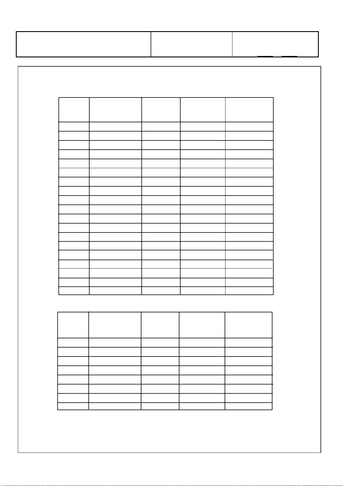
12. Support the Signal Mode
A .D-Sub Mode (VGA or DVI)
LCT4216
CONTINUATION PAGE
NUMBER
7 OF 9 PAGES
NO.
1
2
3
4
5
6
7
8
9
10
11
12
13
14
15
16
17
18
19
Resolution
640 x 400
640 x 480
640 x 480
640 x 480
640 x 480
720 x 400
800 x 600
800 x 600
800 x 600
800 x 600
832 x 624
1024 x 768
1024 x 768
1024 x 768
1152 x 864
1152 x 864
1152 x 864
1280 x 960
1280 x 1024
Horizontal
Frequency
(KHz)
31.47
31.50
35.00
37.50
37.86
31.47
35.16
37.90
46.90
48.08
49.00
48.40
56.50
60.00
54.53
63.86
67.52
60.02
64.00
Vertical
Frequency
(Hz)
70.08
60.00
67.00
75.00
72.81
70.08
56.25
60.32
75.00
72.19
74.00
60.00
70.00
75.00
61.13
70.02
75.02
60.02
60.01
Dot Clock
Frequency
(MHz)
25.17
25.18
30.24
31.50
31.50
28.32
36.00
40.00
49.50
50.00
57.27
65.00
75.00
78.75
80.37
94.51
108.03
108.04
108.00
B.DTV Mode
NO.
1
2
3
4
5
6
7
8
Resolution
480 i
576 i
480p(720x480)
576p(720x576)
720p(1280x720)
720p(1280x720)
1080i(1920x1080)
1080i(1920x1080)
Horizontal
Frequency
(KHz)
15.734
15.625
31.468
31.25
45.00
37.50
28.125
33.75
Vertical
Frequency
(Hz)
59.94
50.00
59.94
50.00
60.00
50.00
50.00
60.00
Dot Clock
Frequency
(MHz)
13.50
13.50
27.00
27.00
74.25
74.25
74.25
74.25
- When the signal received by the Display exceeds the allowed range, a warning message “Out Of Range”
shall appear on the screen.
- You can confirm the input signal format from the “OSD Menu”.
Page 11
Technical Specifications
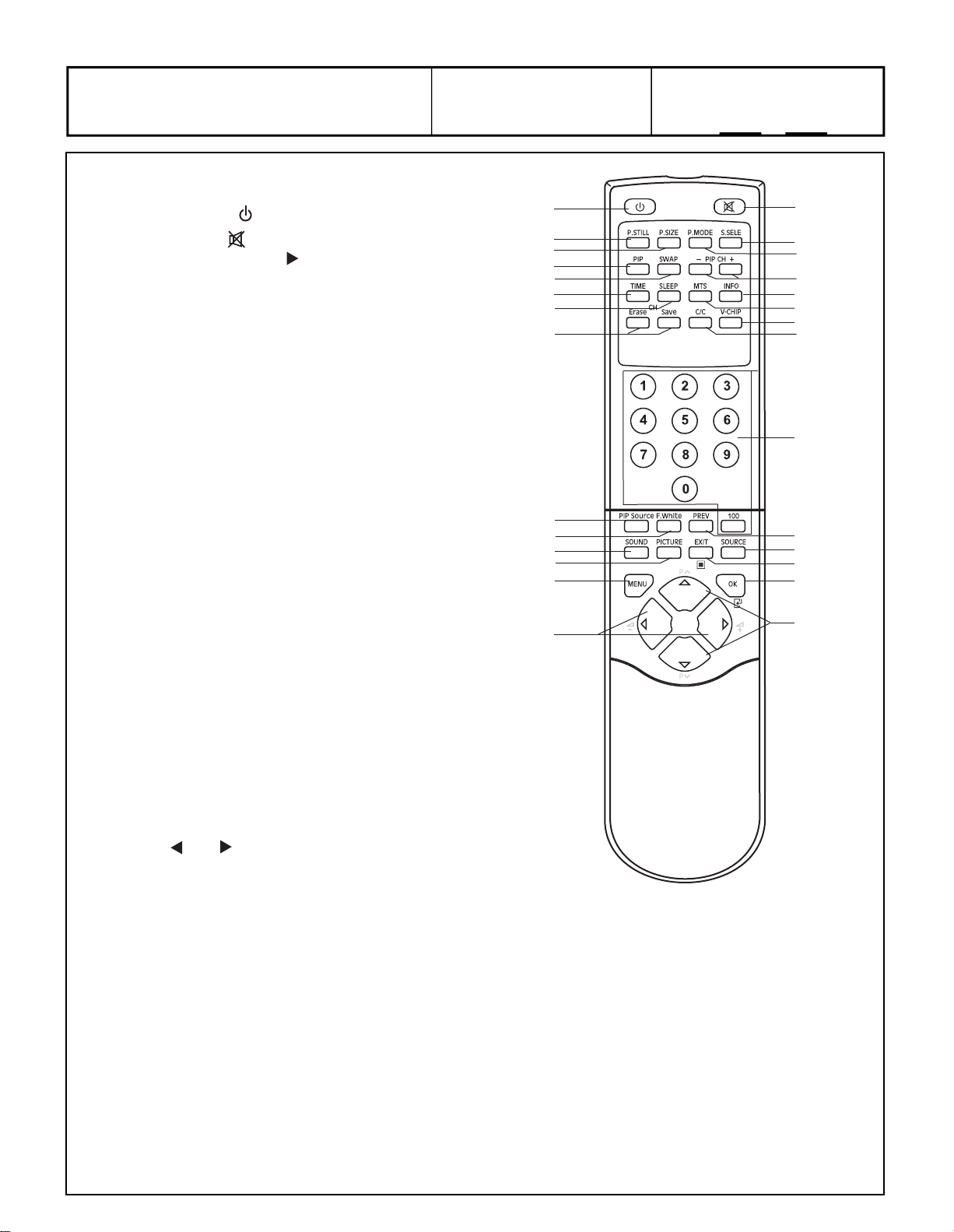
13. Remote Control
LCT-4216
CONTINUATION PAGE
NUMBER
8 OF 9 PAGES
Power ( ): Press to turn on and off.
Mute (
again or press
P.STILL: Press to freeze the picture. Press
again to restore the picture.
P.SIZE: Press to cycles through the picture
size: Normal, Fill Screen, Anamorphic,
Letter Box or TV Mode, Panorama..
P. MODE: Press to cycles through the
picture mode: Normal, Bright, Dark, User.
S.SELE: Press to cycles through the sound
select: Main window sound or Sub window
sound.
PIP: Press to turns on PIP (picture-in picture) feature. Such as Full Screen, PIP or
Split Screen.
SWAP: Press to switches the Main window
or Sub window pictures.
PIP CH+ : Press to select Sub window
Channel Up.
PIP CH- : Press to select Sub window
Channel Down.
TIME: Press to display the current time.
SLEEP: Press repeatedly until it displays
the time in minutes (30 Min, 60 Min, 90 Min,
120 Min, 180 Min or Off ) that you want the
PDP to remain on before shutting off. To
cancel Sleep Time, press SLEEP repeatedly
until Sleep Off appears. And you can press
or to select sleep time shut down.
MTS: Press repeatedly to cycle through the
Multi-channel TV sound (MTS) options:
Mono, Stereo and SAP (Second Audio
Program).
INFO: Press to display on-screen information. Press it again to turn the display off.
CH Erase, CH Save buttons: Press to erase or save channel.
C/C: Press to select the Closed Caption mode.
V-Chip: Press to select the child protect mode.
Number buttons: Press 0~9,100 to select a channel; the channel changes after 2
seconds.
PIP Source: Press to select the signal for Sub Window.(Only for PIP.)
F.WHITE: Press to show a full white picture.
PREV: Press it returns to the last viewed channel.(Only for TV.)
): Press to mute the sound. Press
to restore the sound.
(Continued on next page)
Page 12
CONTINUATION PAGE
Technical Specifications
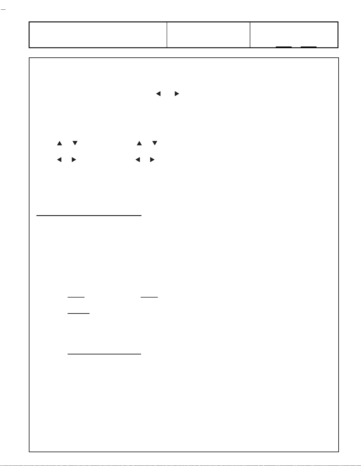
SOUND: Press to select different sound system, such as Normal, Flat, News, Cinema,
User or BBE Digital.
PICTURE: Press to select “BRIGHTNESS”, “COLOR”, “CONTRAST”, ”HUE” or
“SHARPNESS”, and you can use
EXIT: Press to return or exit OSD menu.
SOURCE: Press to select the signal sources directly. Such as TV, AV1, S-VIDEO,
YCbCr, YPbPr, Analog RGB or Digital RGB.
MENU: Press to display the OSD Menu.
OK: Press to enter or confirm.
used for the selection of the program when the OSD Menu is not shown on the screen.
used for the adjustment of volume when the OSD Menu is not shown on the screen.
/ : They are used as / buttons in the OSD Menu screen and they can be
/ : They are used as
/ buttons in the OSD Menu screen and they can be
or to adjust.
LCT-4216
NUMBER
9 OF 9 PAGES
PHYSICAL CHARACTERISTICS
14. Power Cord
Length : 1.8m nominal
Type : optional
15. Cabinet
15.1 Color
: “Black” colour as defined by colour plaque reference number
15.2 Weight
Net weight : 114.7lbs (52.1kg)
Gross weight : 139.2lbs(63.1kg)
15.3 Dimensions(with stand)
Width : 57 inches (1444mm)
Height : 45.59 inches (1155mm)
Depth : 14.61 inches (370mm)
Page 13
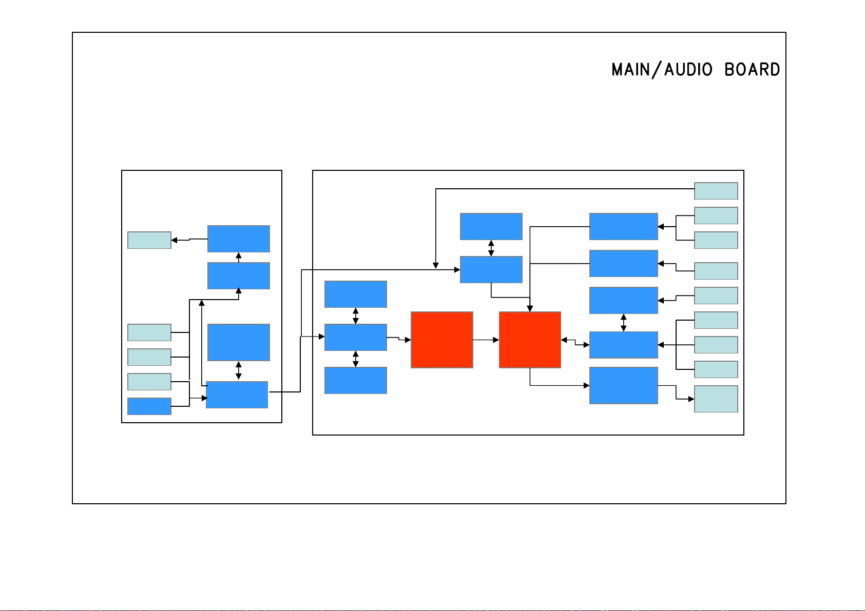
Block Diagram
Speaker
SCART1
Video2
S-Video
Tuner x 2
Sub Board
TDA8946
Audio AMP
MSP34x0G
Audio Decoder
uPD64083
Separator
M52790
A/V Switch
3D Y/C
Main Board
Z86229
V-Chip / CC
VPC3230D
Vide Decoder
SDA5550
TVText Pro
PW1231
De-
Interlacer
Z86229
V-Chip / CC
VPC3230D
Video Decoder
Processor
PW181
Image
AD9883A
ADC
Sil161B
DVI Receiver
MAX232C
RS232C
W78E65B
System Control
THC63LVDM83
LVDS
Transmitter
YCrCb
YPbPr
D-SUB15
DVI
D-SUB9
IR
Keypad
LED
LDVS
Header
Page 14

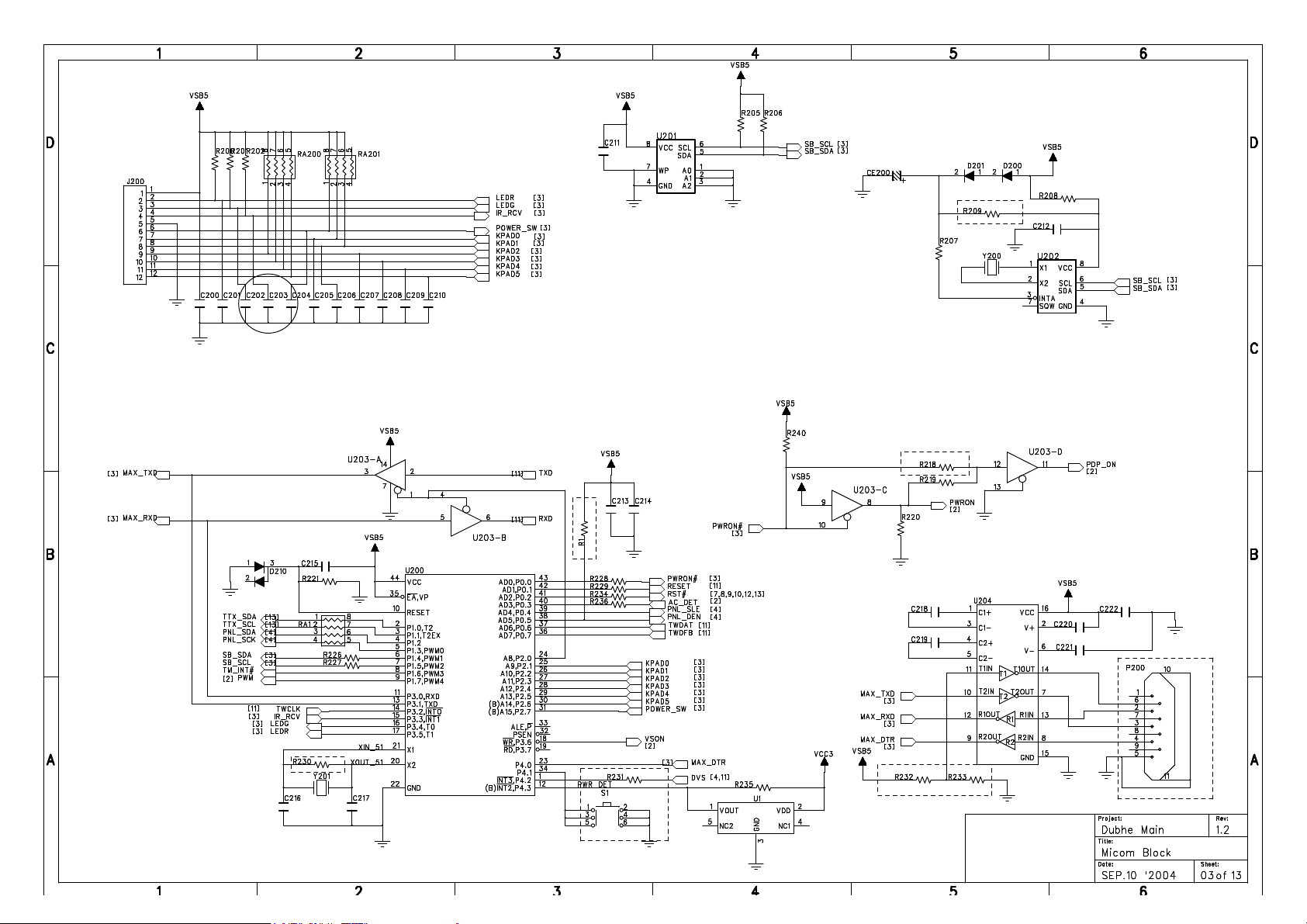
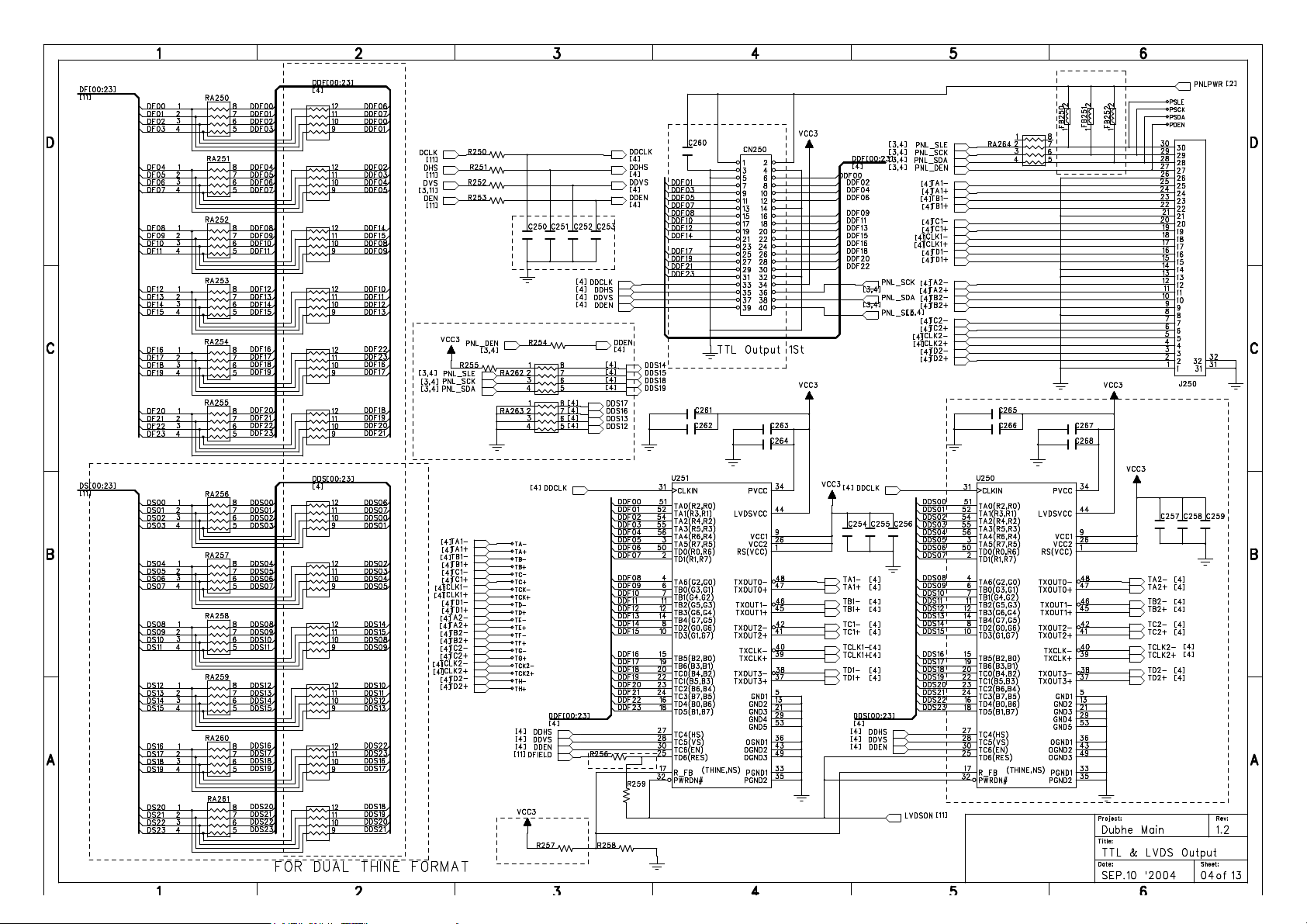
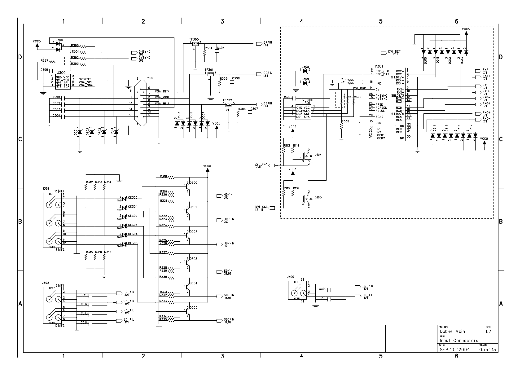
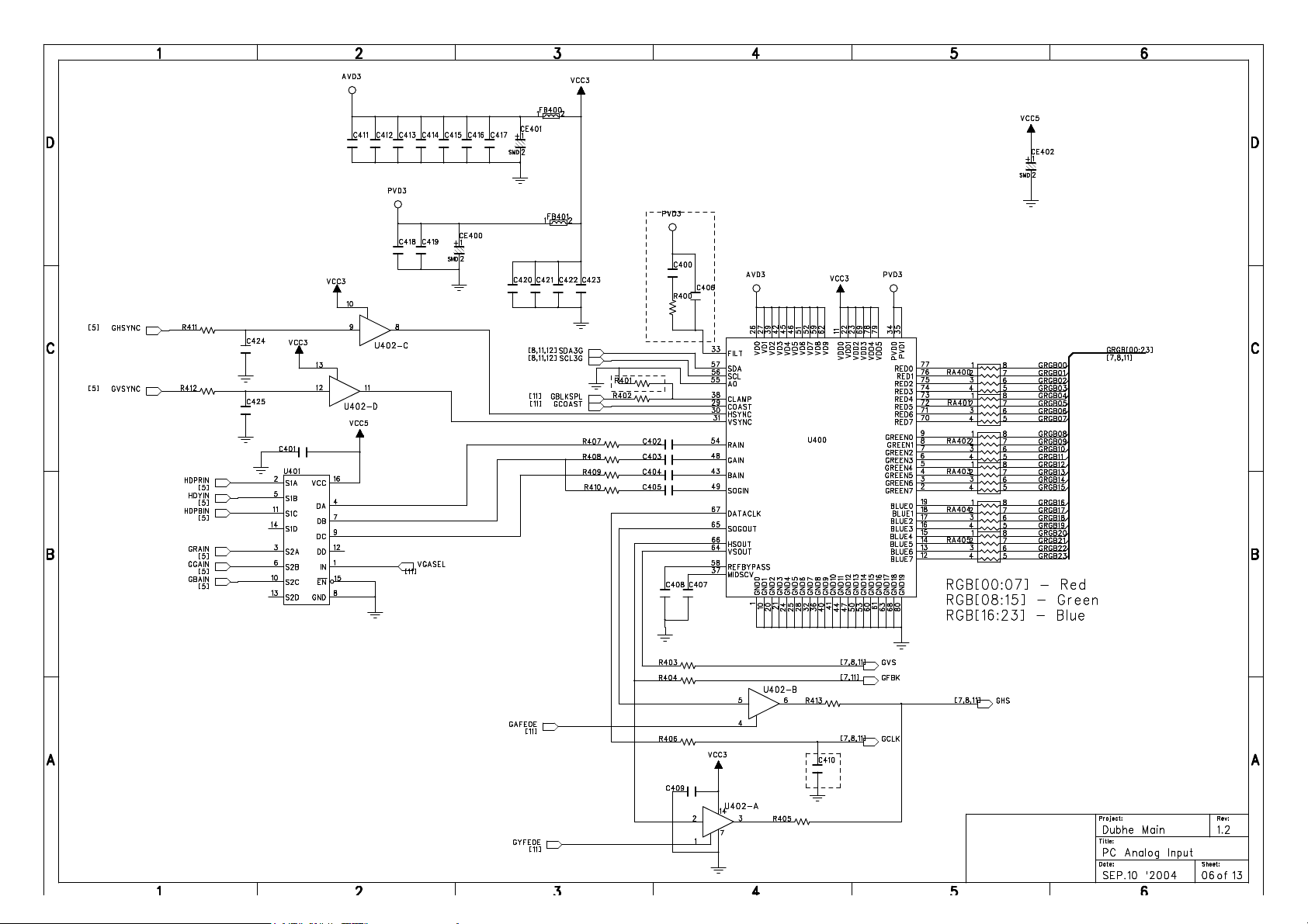
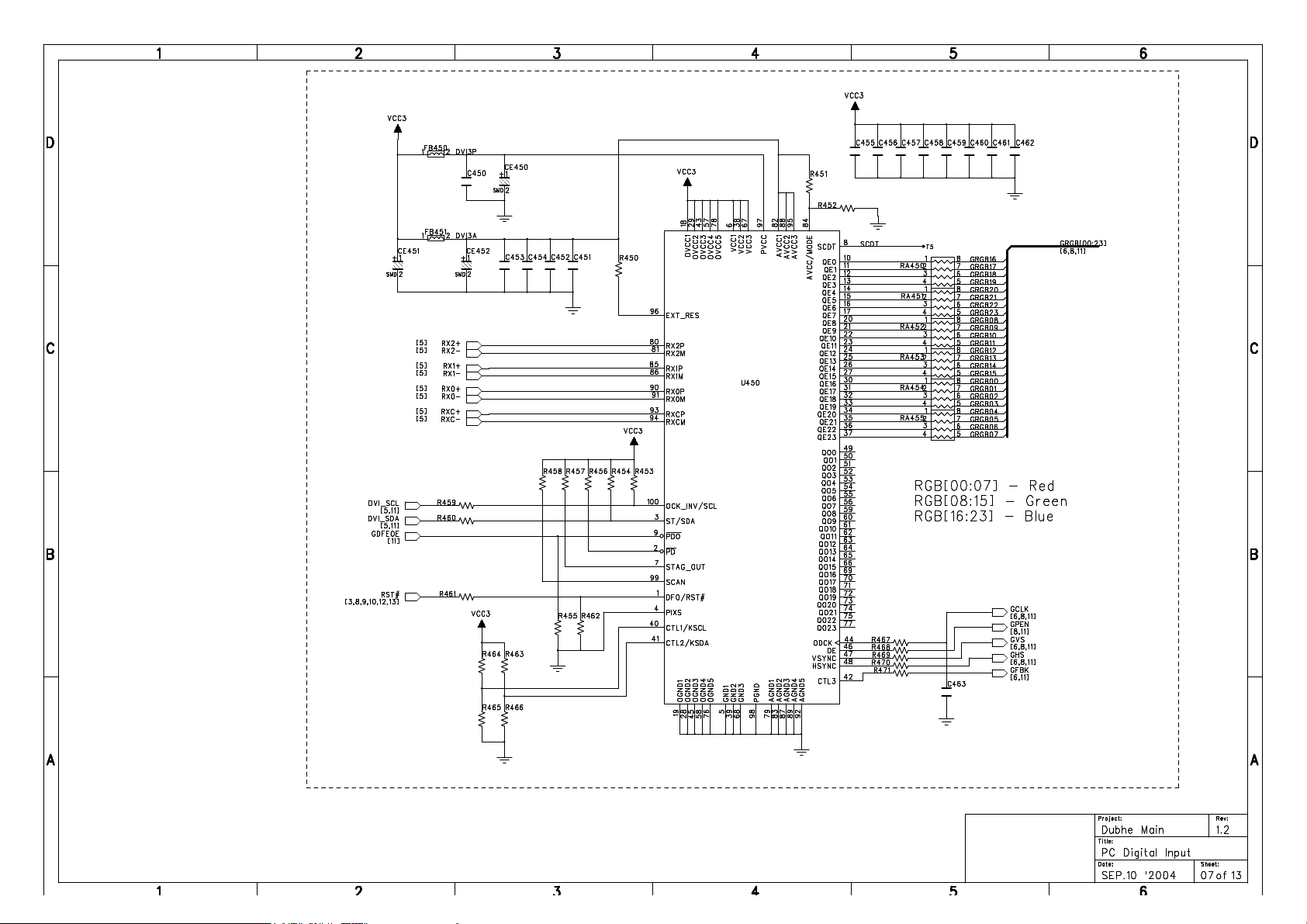
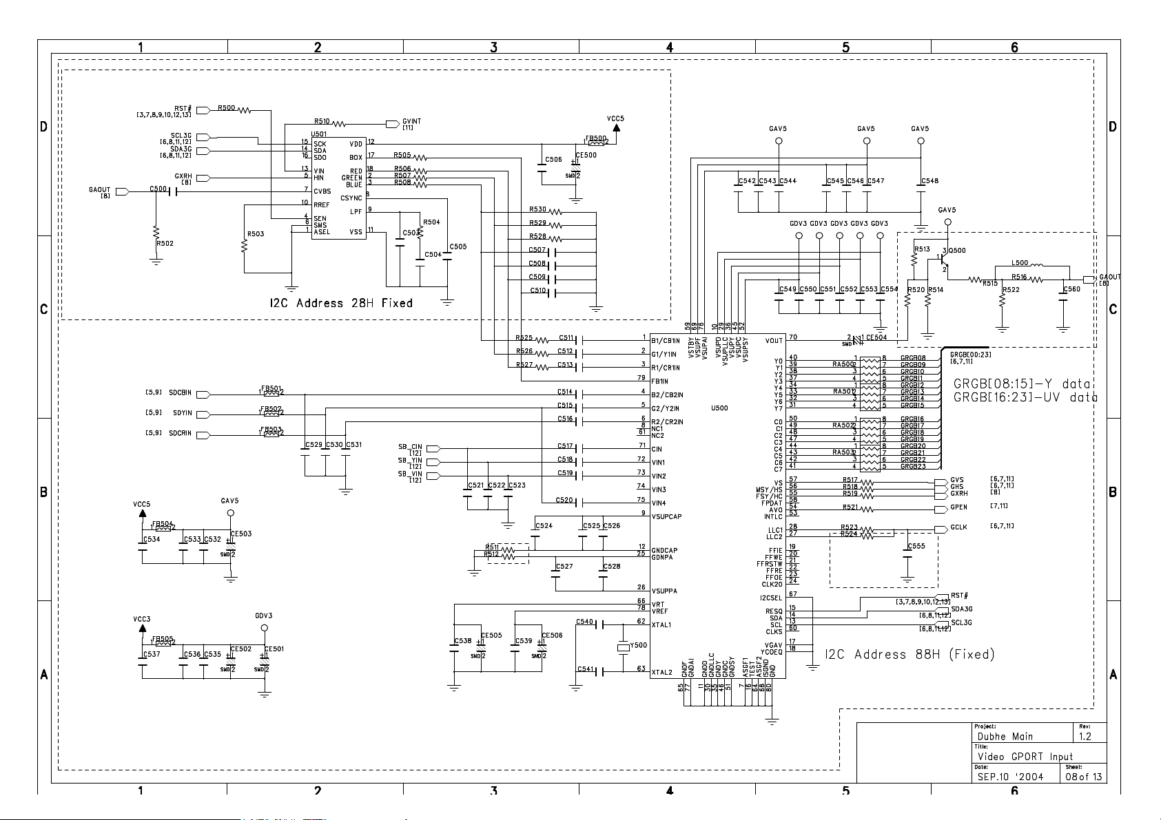
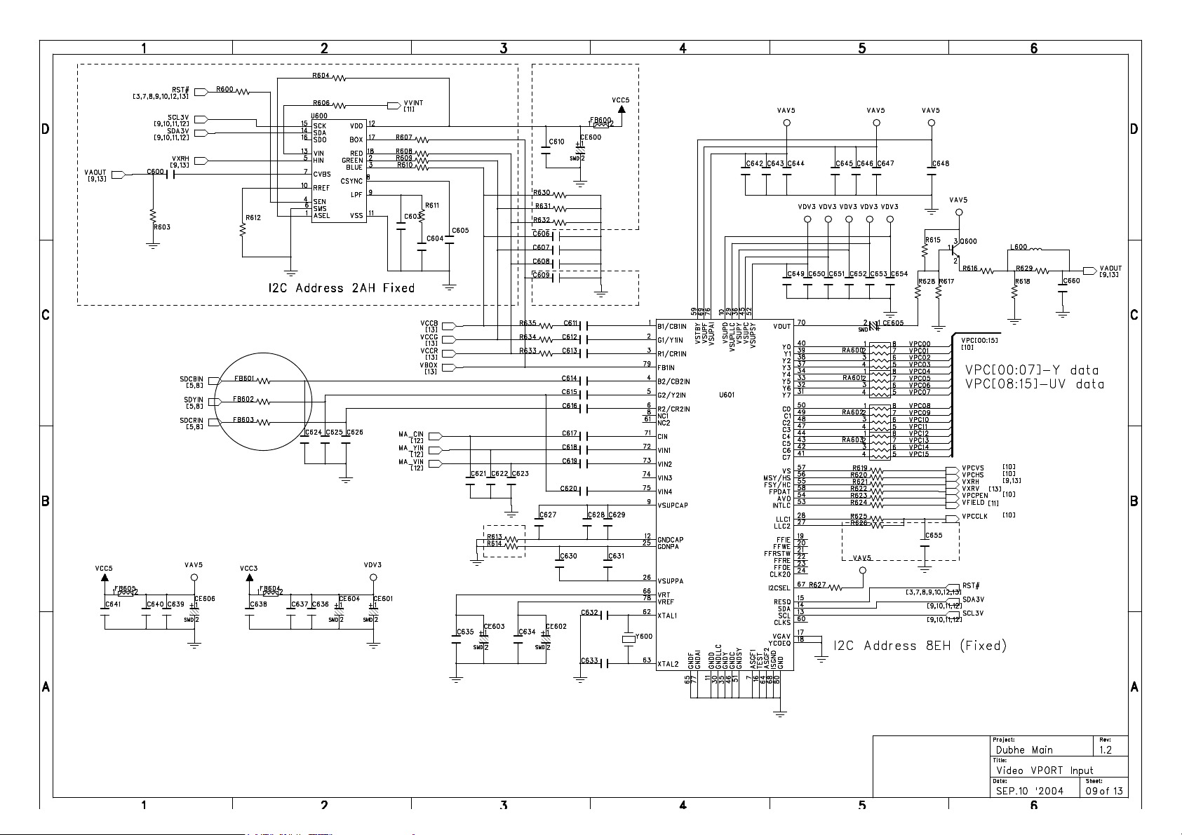
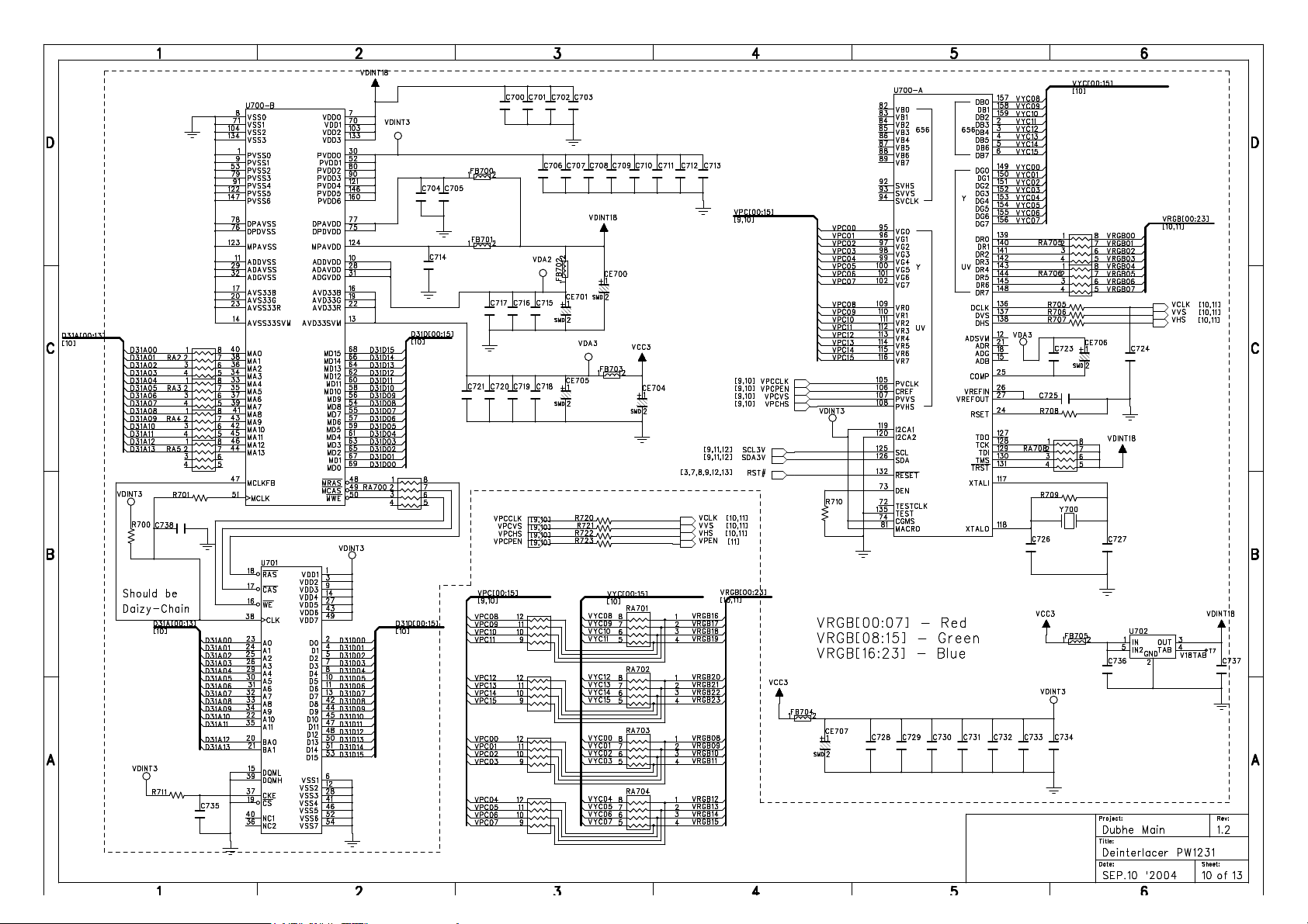
Circuit Diagram
- Power supply board of LCD Module, PSM250-405
- Main (Video) board
- Audio/Tuner board
- Keypad board
- Remote control receiver board
- Remote control board
Page 15
B+
5
AC+
AC-
3
+12V
CN-A
CN-B
+5V
+5VSB
ON/OFF
VC
AC+
AC-
B+
VC
5
VCC
B
Page 16
PC5:2
5
+5VSB
B+
C
ON/OFF
VCC
B-
CN-A
CN-B
B+
VC
1
+24V
+24V
Q14
R93
A
+12V
+5V
+12V
+24V
ZD5
+12V
+12V
+5VSB
+12V
VC
3
+5V
5
REF
C
VC
A
B
+5V
Page 17

Page 18
Page 19
Page 20
Page 21
Page 22
Page 23
Page 24
Page 25
Page 26
Page 27
Page 28
Page 29

Page 30

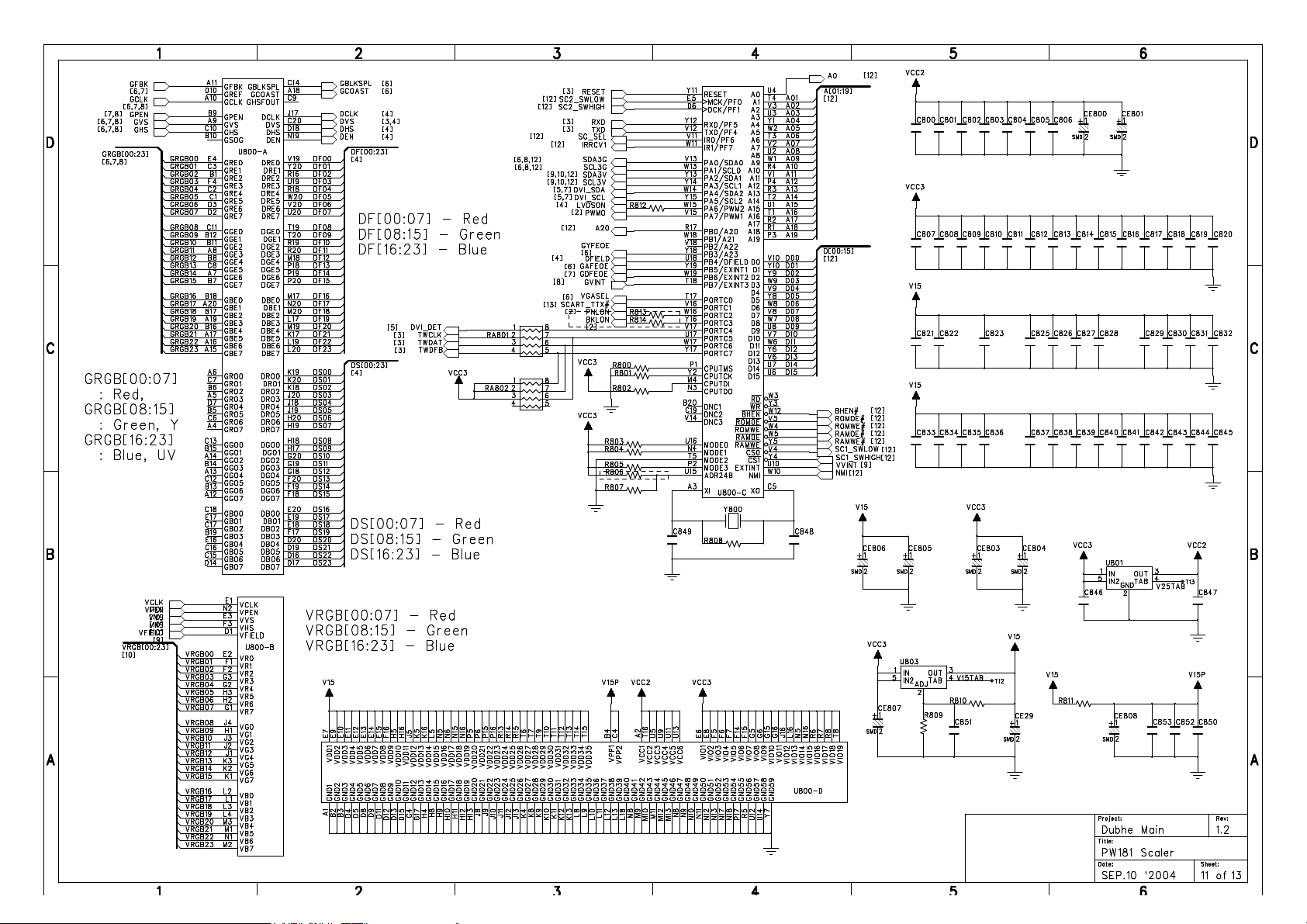
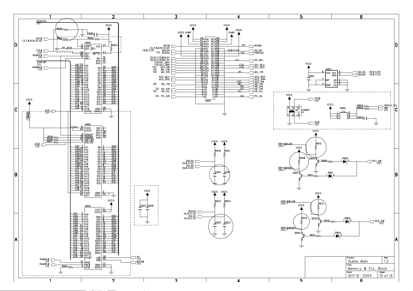
Dbh1S4909V12.sch-1 - Thu Oct 07 00:30:41 2004
Page 31

Dbh1S4909V12.sch-2 - Thu Oct 07 00:30:42 2004
Page 32

Dbh1S4909V12.sch-3 - Thu Oct 07 00:30:43 2004
Page 33

Dbh1S4909V12.sch-4 - Thu Oct 07 00:30:45 2004
Page 34

Dbh1S4909V12.sch-5 - Thu Oct 07 00:30:47 2004
Page 35

Dbh1S4909V12.sch-6 - Thu Oct 07 00:30:49 2004
Page 36

Dbh1S4909V12.sch-7 - Thu Oct 07 00:30:50 2004
Page 37

DUBHE OSD Ver1.1_NAKS.sch-1 - Mon Oct 18 11:47:11 2004
Page 38

0025-TTX.sch-1 - Thu May 05 23:47:54 2005
Page 39

Basic Operations & Circuit Description
Main Electric Components
(1). MODULE:
There are 1 pc. panel and 3 pcs. PCB including 2 pcs. INVERTER
board(L&R), 1 pc. T-CONTROL board,
(2).SIGNAL PROCESS
There are 7 pcs. PCBs including
1 pc. Tuner board,
1 pc. Audio board,
1 pc. Main digital board,
1 pc. Keypad board,
1 pc. Remote Control Receiver board,
2 pc. L/R Speakers converter board.
(3).POWER
There are 1 pc. PCB for power.
Page 40

EXTERNAL
SPEAKER R
INVERTER R
KEY&REMOTE
CONTROL BOARD
MAIN DIGITAL
BOARD
POWER BOARD
INVERTER L
EXTERNAL
SPEAKER L
SIGNAL OUT
TERMINAL
T-CONTROL BOARD
TUNER&AUDI
O BOARD
STAND
EXTERNAL SPEAKER L
TERMINAL
EXTERNAL SPEAKER R
TERMINAL
42LCD PANEL
Page 41

PCB function
1. Power:
(1). Input voltage: AC 100V~240V, 47Hz~63Hz.
Input range: AC 90V(Min)~264V(Max) auto regulation.
(2). To provide power for PCBs.
a). +24V for Inverter.
b). +5Vsb for standby,
c). +5V for signal power,
d). +18V for Audio Amp power and converter to +12V for Lvds power.
2. Main (Video InterFace) board:
(1).Decoder the video signal (TV,CVBS,S-VIDEO,YCbCr) from analog to digital
signal.
(2).Converter the Video signals( TV,CVBS,S-VIDEO,YCbCr) and graphics signal
(DVI,VGA,YPbPr) from internace to progressive,
(3). Converter the Digital to fit the panel display mode and output the LVDS
signal to Panel.
3. Tuner Board:
Convert TV RF signal to video and audio signal to Main board.
4. Audio board:
(1).Decoder the TV SIF signal to audio signal,
(2).Converter the audio to audio Ampifile and out put to the external speaker.
(3).3D comb-filter
5. KEYBOARD
To get the main button control on LCD_TV as SOURCE,MENU,
CHANEL +,CHANEL -, VOL +,VOL-, STANDBY functions.
6. Remote control board
Receive the remote signal and active for the control.
7. T-CONTROL board
Converter the LVDS signal to the digital signal for fitting the PANEL.
8. INVERTER board
Converter the low DC voltage +24V to high AC voltage about AC600V to drive
the backlight.
Page 42

PCB failure analysis
1. CONTROL:
a. Abnormal noise on screen.
b. No picture.
2. MAIN (VIDEO):
a. Lacking color, Bad color scale.
b. No voice.
c. No picture but with signals output, OSD and back light.
d. Abnormal noise on screen.
3. POWER:
No picture, no power output.
Basic operation of LCD-TV
1. After turning on power switch, power board sends 5Vst-by Volt to Micro
Processor IC waiting for ON signals from Key Switch or Remote Receiver.
2. When the ON signal from Key Switch or Remote Receiver is detected, Micro
Processor will send ON Control signals to Power. Then Power sends (5Vsc,
18Vsc, 24V and RLY ON, Vs ON) to PCBs working. This time VIF will send
signals to display back light, OSD on the panel and start to search available
signal sources. If the audio signals input, them will be amplified by Audio AMP
and transmitted to Speakers.
3. If some abnormal signals are detected (for example: over volts, over current,
over temperature and under volts), the system will be shut down by Power off.
Page 43

LCD basic display theory.
When an electrical field is applied to the LC planes, the LC molecules re-align
themselves so that they are parallel to the electrical field. This electrical process
is known as twisted nematic field effect or TNFE. In this alignment, polarized
light is not twisted as it passes through the LC material (see Diagram 3A and
3B). If the front polarizer is oriented perpendicular to the rear polarizer, light will
pass through the energized display but will be blocked by the rear polarizer. An
LCD in this form is acting as a light shutter.
Displays with variable characters are created by selectively etching away the
conductive surface that was originally deposited on the glass. Etched areas
become the display’s background; unetched areas become the display’s
characters.
Diagram 3A. The “off” state of a TN LCD-the LC molecules form a twist and therefore
cause polarized light to twist as it passes through.
Diagram 3B. The “on” state-the electrical field re-aligns the LC molecules so they do
not twist the polarized light.
Page 44

Main IC Specifications
- PW181 Image Processor, Scaler
- PW1231 Digital Video Signal Processor
- uPD64083 Three –Dimensional Y/C Separation LSI
With On-Chip Memory
- AD9883A 110MSPS/140MSPS Analog Interface
- VPC 323XD Comb-filter Video Processor
- Si161B Panel Link Receiver
- Z86229 NTSC Line 21 CCD decorder
- MSP34x0G Multistandard Sound Processor
Page 45

PW181
Product Specification
General Description
The PW181 ImageProcessor is a highly integrated
“system-on-a-chip” that interfaces computer graphics and
video inputs in virtually any format to a fixed-frequency flat
panel display.
Computer and video images from NTSC/PAL to WUXGA
at virtually any refresh rate can be resized to fit on a fixedfrequency target display device with any resolution up to
WUXGA. Video data from 4:3 aspect ratio NTSC or PAL
and 16:9 aspect ratio HDTV or SDTV is supported. Multiregion, nonlinear scaling allows these inputs to be resized
optimally for the native resolution of the display.
Advanced scaling techniques are supported, such as
format conversion using multiple programmable regions.
Three independent image scalers coupled with frame
locking circuitry and dual programmable color lookup
tables create sharp images in multiple windows, without
user intervention.
Embedded SDRAM frame buffers and memory controllers
perform frame rate conversion and enhanced video
processing completely on-chip. A separate memory is
dedicated to storage of on-screen display images and
CPU general purpose use.
Advanced video processing techniques are supported
using the internal frame buffer, including motion adaptive,
temporal deinterlacing with film mode detection. When
used in combination with the new third-generation scaler,
this advanced video processing technology delivers the
highest quality video for advanced displays.
Both input ports support integrated DVI 1.0 content
protection using standard DVI receivers.
A new advanced OSD Generator with more colors and
larger sizes supports more demanding OSD applications,
such as on-screen programming guides. When coupled
with the new, faster, integrated microprocessor, this OSD
Generator supports advanced OSD animation techniques.
Video
TV
Signal
Input
TV Tu n e r
Com puter
Video
Decoder
ADC/
TMDS
Crystal
PW181
TV
Signal
Com puter
TV Tu n e r
Video
Input
ADC/
TMDS
Video
Decoder
PW181 System Block Diagram
ROM
Features
• Third-generation, two-dimensional filtering techniques
• Third-generation, advanced scaling techniques
• Second-generation Automatic Image Optimization
• Frame rate conversion
• Video processing
• On-Screen Display (OSD)
• On-chip microprocessor
• JTAG debugger and boundary scan
• Picture-in-picture (PIP)
• Multi-region, non-linear scaling
• Hardware 2-wire serial bus support
Applications
• Multimedia Displays
• Plasma Displays
• Digital Television
Device Application Package
PW181-10V Up to XGA Displays
PW181-20V Up to UXGA Displays
352 PBGA
Dis pla y
Programmable features include the user interface, custom
start-up screen, all automatic imaging features, and
special screen effects.
PRELIMINARY / CONFIDENTIAL
Page 46

110 MSPS/140 MSPS Analog Interface
a
FEATURES
140 MSPS Maximum Conversion Rate
300 MHz Analog Bandwidth
0.5 V to 1.0 V Analog Input Range
500 ps p-p PLL Clock Jitter at 110 MSPS
3.3 V Power Supply
Full Sync Processing
Sync Detect for “Hot Plugging”
Midscale Clamping
Power-Down Mode
Low Power: 500 mW Typical
4:2:2 Output Format Mode
APPLICATIONS
RGB Graphics Processing
LCD Monitors and Projectors
Plasma Display Panels
Scan Converters
Microdisplays
Digital TV
R
AIN
G
AIN
B
AIN
HSYNC
COAST
CLAMP
FILT
SCL
SDA
for Flat Panel Displays
FUNCTIONAL BLOCK DIAGRAM
CLAMP
CLAMP
CLAMP
SYNC
PROCESSING
AND CLOCK
GENERATION
SERIAL REGISTER
AND
A
0
POWER MANAGEMENT
A/D
A/D
A/D
AD9883A
8
R
OUTA
8
G
OUTA
8
B
OUTA
MIDSCV
DTACK
HSOUT
VSOUT
SOGOUT
REF
AD9883A
REF
BYPASS
GENERAL DESCRIPTION
The AD9883A is a complete 8-bit, 140 MSPS monolithic analog
interface optimized for capturing RGB graphics signals from
personal computers and workstations. Its 140 MSPS encode
rate capability and full power analog bandwidth of 300 MHz
supports resolutions up to SXGA (1280 × 1024 at 75 Hz).
The AD9883A includes a 140 MHz triple ADC with internal
1.25 V reference, a PLL, and programmable gain, offset, and
clamp control. The user provides only a 3.3 V power supply,
analog input, and Hsync and COAST signals. Three-state
CMOS outputs may be powered from 2.5 V to 3.3 V.
The AD9883A’s on-chip PLL generates a pixel clock from the
Hsync input. Pixel clock output frequencies range from 12 MHz to
140 MHz. PLL clock jitter is 500 ps p-p typical at 140 MSPS.
When the COAST signal is presented, the PLL maintains its
output frequency in the absence of Hsync. A sampling phase
adjustment is provided. Data, Hsync, and clock output phase
relationships are maintained. The AD9883A also offers full sync
processing for composite sync and sync-on-green applications.
A clamp signal is generated internally or may be provided by
the user through the CLAMP input pin. This interface is fully
programmable via a 2-wire serial interface.
Fabricated in an advanced CMOS process, the AD9883A is
provided in a space-saving 80-lead LQFP surface-mount plastic
package and is specified over the 0°C to 70°C temperature range.
REV. A
Information furnished by Analog Devices is believed to be accurate and
reliable. However, no responsibility is assumed by Analog Devices for its
use, nor for any infringements of patents or other rights of third parties that
may result from its use. No license is granted by implication or otherwise
under any patent or patent rights of Analog Devices.
One Technology Way, P.O. Box 9106, Norwood, MA 02062-9106, U.S.A.
Tel:
Fax:
Page 47

PW1231A
Product Specification
General
The PW1231A is a high-quality, digital video signal
processor that incorporates Pixelworks’ patented
deinterlacing, scaling, and video enhancement
algorithms. The PW1231A accepts industry-standard
video formats and resolutions, and converts the input into
many desired output formats.The highly efficient video
algorithms result in excellent quality video.
The PW1231A combines many functions into a single
device, including a memory controller, auto-configuration,
and others. This high level of integration enables simple,
flexible, cost-effective solutions that require fewer
components.
Crysta l
Video
PW1231A
System Block Di a gra m
Video
Decoder
PW1231A
PW1231AL
SDRAM
Digital
Output
Features
• Built-In Memory Controller
• Motion-Adaptive Deinterlace Processor
• Intelligent Edge Deinterlacing
• Digital Color/Luminance Transient Improvement (DCTI/DLTI)
• Interlaced Video Input Options, including NTSC and PAL
• Independent horizontal and vertical scaling
• Copy Protection
• Two-Wire Serial Interface
8100 SW Nyberg Road
Tualatin, OR 97062 USA
Telephone: 503.612.6700
FAX: 503.612.6713
www.pixelworks.com
Applications:
For use with Digital Displays
• Flat-Panel (LCD, DLP) TVs
• Rear Projection TVs
• Plasma Displays
• LCD Multimedia Monitors
• Multimedia Projectors
Device Application Package
PW1231A
PW1231AL
NOTE: “L” denotes lead (Pb) free
Up to XGA 160-pin PQF
P/N 001-0097-00 Rev B
PRELIMINARY—CONFIDENTIAL
July 2003
Page 48

DATA SHEET
MOS INTEGRATED CIRCUIT
PD64083
µµµµ
THREE-DIMENSIONAL Y/C SEPARATION LSI WITH ON-CHIP MEMORY
DESCRIPTION
The µPD64083 realizes a high precision Y/C separation and a noise reduction by the three-dimension signal
processing for NTSC signal.
This product has the On-chip 4-Mbit memory for flame delay, 2ch of high precision internal 10-bit A/D converter, and
adapting 10-bit signal processing (only for luminance signal) and high picture quality. The
single-chip system of 3D Y/C separation.
This LSI includes the Wide Clear Vision ID signal (Japanese local format) decoder and ID-1 signal decoder.
PD64083 is completely
µ
FEATURES
•
On-chip 4-Mbit frame delay memory.
•
4 Operation mode (Compatible to the µPD64082)
Motion adaptive 3D Y/C separation (for Composite video input)
Frame recursive Y/C NR (for Y/C separated video input)
Frame comb type YNR + 1H delayed C signal (for Y/C separated video input)
2D Y/C separation + Frame recursive Y/C NR (for Composite video input)
•
Embedded A/D converter (2ch), D/A converter (2ch), clock generator.
•
Embedded Y coring, Vertical enhancer, Peaking filter, and Noise detector.
•
Embedded WCV-ID decoder and ID-1 decoder.
•
I2C bus control.
•
Dual power supply of 2.5 V and 3.3 V.
For digital : DV
For analog : AV
For DRAM : DV
For I/O : DV
DDIO
= 2.5 V
DD
= 2.5 V
DD
DDRAM
= 3.3 V
= 2.5 V
ORDERING INFORMATION
Part number Package
PD64083GF-3BA 100-pin plastic QFP (14 × 20)
µ
Document No. S15849EJ1V0DS00 (1st edition)
Date Published January 2002 NS CP (K)
Printed in Japan
2
Page 49

PRELIMINARY DATA SHEET VPC 323xD
Comb Filter Video Processor
1. Introduction
The VPC 323xD is a high-quality, single-chip video
front-end, which is targeted for 4: 3 and 16:9, 50/60-Hz
and 100/120 Hz TV sets. It can be combined with other
members of the DIGIT3000 IC family (such as
DDP 3 31x) and/or it can be used with 3rd-party products.
The main features of the VPC 323xD are
– high-performance adaptive 4H comb filter Y/C sepa-
rator with adjustable vertical peaking
– multi-standard color decoder PAL/NTSC/SECAM
including all substandards
– four CVBS, one S-VHS input, one CVBS output
– two RGB/YC
component inputs, one Fast Blank
rCb
(FB) input
– integrated high-quality A/D converters and associ-
ated clamp and AGC circuits
– multi-standard sync processing
– linear horizontal scaling (0.25 ... 4), as well as
non-linear horizontal scaling ‘Panoramavision’
– PAL+ preprocessing
– peaking, contrast, brightness, color saturation and
tint for RGB/YC
and CVBS/S-VHS
rCb
– high-quality soft mixer controlled by Fast Blank
1
1
1
----- -
-- -
– PIP processing for four picture sizes ( , or
1
---
of normal size) with 8-bit resolution
36
---
,,
4
16
9
– 15 predefined PIP display configurations and expert
mode (fully programmable)
– control interface for external field memory
2
–I
C-bus interface
– one 20.25-MHz crystal, few external components
– 80-pin PQFP package
1.1. System Architecture
Fig.1–1 shows the block diagram of the video processor
– line-locked clock, data and sync, or 656-output
interface
CIN
VIN1
VIN2
VIN3
VIN4
VOUT
RGB/
YCrCb
FB
RGB/
YCrCb
Analog
Front-end
AGC
2×ADC
Analog
Component
Front-End
4 x ADC
Adaptive
Comb
Filter
NTSC
PAL
Y/G
Processing
U/B
V/R
FB FB
Matrix
Contrast
Saturation
Brightness
Tint
Color
Decoder
NTSC
PAL
SECAM
Saturation
Tint
Y
Cr
Cb
Y
Cr
Cb
Mixer
Y
2D Scaler
Panorama
Cr
Cb
Brightness
Clock
Gen.
PIP
Mode
Contrast
Peaking
2
I
C Bus
Output
Formatter
ITU-R 656
ITU-R 601
Memory
Control
Sync
+
Clock
Generation
Y OUT
CrCb
OUT
YCOE
FIFO
CNTL
LL C lock
H Sync
V Sync
AVO
Fig.1–1:Block diagram of the VPC323xD
Micronas
2
C Bus20.25 MHz
I
Page 50

SiI 161B PanelLink® Receiver
Data Sheet
General Description Features
The SiI 161B receiver uses PanelLink Digital
technology to support high-resolution displays up to
UXGA (25-165MHz). This receiver supports up to true
color panels (24 bits per pixel, 16M colors) with both
one and two pixels per clock.
All PanelLink products are designed on a scaleable
CMOS architecture, ensuring support for future
performance enhancements while maintaining the
same logical interface. System designers can be
assured that the interface will be stable through a
number of technology and performance generations.
PanelLink Digital technology simplifies PC and display
interface design by resolving many of the system level
issues associated with high-speed mixed signal design,
providing the system designer with a digital interface
solution that is quicker to market and lower in cost.
• Low Power Operation: 280mA max. current
consumption at 3.3V core operation
• Time staggered data output for reduced ground
bounce and lower EMI
• Sync Detect feature for Plug & Display
• Cable Distance Support: over 5m with twisted-
pair, fiber-optics ready
• ESD tolerant to 5kV (HBM on all pins)
• Compliant with DVI 1.0 (DVI is backwards
compatible with VESA
®
P&DTM, FPDI-2
DFP)
• HSYNC de-jitter circuitry enables stable operation
even when HSYNC contains jitter
• Low power standby mode
• Automatic entry into standby mode with clock
detect circuitry
• Standard and Pb-free packages (see page 25).
August 2002
TM
and
Page 51

4'.+/+0#4; 41&7%6#2'%+(+%#6+10
<
+0'
'%1&'4
• Complete Stand-Alone Line 21 Decoder for Closed-
Captioned and Extended Data Services (XDS)
• Preprogrammed to Provide Full Compliance with
EIA–608 Specifications for Extended Data Services
• Automatic Extraction and Serial Output of Special
XDS Packets (Time of Day, Local Time Zone, and
Program Blocking)
• Programmable XDS Filter for a Specific XDS Packet
• Cost-Effective Solution for NTSC Violence Blocking
inside Picture-in-Picture (PiP) Windows
!"
#$%
&%
" '
• Minimal Communications and Control Overhead Pro-
vide Simple Implementation of Violence Blocking,
Closed Captioning, and Auto Clock Set Features
• Programmable, On-Screen Display (OSD) for Creat-
ing Full Screen OSD or Captions inside a Picture-inPicture (PiP) Window
• User-Programmable Horizontal Display Position for
easy OSD Centering and Adjustment
2
• I
C Serial Data and Control Communication
• Supports 2 Selectable I
2
C Addresses
Capable of processing Vertical Blanking Interval (VBI)
data from both fields of the video frame in data, the Z86229
Line 21 Decoder offers a feature-rich solution for any television or set-top application. The robust nature of the
Z86229 helps the device conform to the transmissionformat
defined in the Television Decoder Circuits Act of 1990, and
in accordance with the Electronics Industry Association
specification 608 (EIA–608).
The Line 21 datastream can consist of data fromseveral data
channels multiplexed together. Field 1 consists of four data
channels: two Captions and two Texts. Field 2 consists of
five additional data channels: two Captions, two Texts, and
Extended Data Services (XDS). The XDS data structure is
defined in EIA–608. The Z86229 can recover and display
data transmitted on any of these nine data channels.
The Z86229 can recover and output to a host processor via
2
C serial bus. The recovered XDS data packet is further
the I
defined in the EIA–608 specification. The on-chip XDS filters in the Z86229 are fully programmable, enabling recovery of only those XDS data packets selectedby the user. This
functionality allows the device to extract the required XDS
information with proper XDS filter setup for compatibility
in a variety of TVs, VCRs, and Set-Top boxes.
In addition, the Z86229 is ideally suited to monitor Line 21
video displayed in a PiP window for violence blocking,
CCD, and other XDS data services. A block diagram of the
Z86229 is illustrated in Figure 1.
Page 52

PRELIMINARY DATA SHEET MSP 34x0G
Multistandard Sound Processor Family
Release Note: Revision bars indicate significant
changes to the previous edition. The hardware and
software description in this document is valid for
the MSP 34x0G version B8 and following versions.
1. Introduction
The MSP 34x0G family of single-chip Multistandard
Sound Processors covers the sound processing of all
analog TV-Standards worldwide, as well as the NICAM
digital sound standar ds. The full TV sound processin g,
starting with analog sound IF signal-in, down to processed analog AF-out, is performed on a single chip.
Figure 1–1 shows a simplified functional block diagram
of the MSP 34x0G.
This new generation of TV sound processing ICs now
includes versions for processing the multichan nel television sound (MTS) signal conforming to the standard
recommended by the Broadcast Television Systems
Committee (BTSC). The DBX noise reduction, or alternatively, Micronas Noise Reduction (MNR) is performed alignment free.
Other processed standards are the Japanese FM-FM
multiplex standard (EIA-J) and the FM Stereo Radio
standard.
Current ICs have to perform adjustment procedu res in
order to achieve good stereo sepa ration for BTSC and
EIA-J. The MSP 34x0G has optimum stereo performance without any adjustments.
All MSP 34xxG versions are pin compatible to the
MSP 34xxD. Only minor modifications are necessary
to adapt a MSP 34xxD controlling software to the
MSP 34xxG. The MSP 34x0G further simplifies controlling software. St andard selection requi res a single
2
C transmission only.
I
The MSP 34x0G has built-in automatic functions: The
IC is able to detect the actual sound standard automatically (Automatic Standard Detection). Furthermore,
pilot levels and identification sign als can be evaluated
internally with subsequent switching between mono/
stereo/bilingual; no I
2
C interaction is necessar y (Auto-
matic Sound Selectio n) .
The MSP 34x0G can handle ver y high FM deviations
even in conjunction with NICAM processing. This is
especially impor tant for the introduction of NICAM in
China.
The ICs are produced in submicron CMOS technology.
The MSP 34x0G is available in the following packages:
PLCC68 (not intended for new design), PSDIP64,
PSDIP52, PQFP80, and PLQFP64.
Sound IF1
Sound IF2
I2S1
I2S2
SCART1
SCART2
SCART3
SCART4
MONO
ADC
SCART
DSP
Input
Select
De-
modulator
ADC
Pre-
processing
Prescale
Prescale
Fig. 1–1: Simplified functional block diagram of the MSP 34x0G
Loud-
speaker
Sound
Processing
Headphone
Sound
Processing
Source Select
DAC
DAC
DAC
DAC
SCART
Output
Select
Loudspeaker
Subwoofer
Headphone
I2S
SCART1
SCART2
Micronas
Page 53

SPECIFICATION
POWER SPECIFICATION
MODEL NO.
REVISION
PSM250-405
01
1. REVISION HISTORY :
Date Rev. Page Summary
2005.03.14 00 All
2005.03.15 01 6 Change 24V peak power 8A @ 3 minutes.
DA TE
2005.03.14
REV: 01 PAGE. 3
Page 54

SPECIFICATION
MODEL NO.
REVISION
PSM250-405
01
DA TE
2005.03.14
2. SCOPE :
This specification describes a full range of AC input with DC output switching mode power supply, it is
an Open Frame type with build in active power factor correction circuit, the PSU performance driver for
a Smart Switching-mode with Green / Power-savor function.
3. ELECTRICAL SPECIFICATIONS :
3.1. AC INPUT CHARACTERISTICS :
:
3.1.1. Input voltage :
For the outputs to be within their specified limits, the input voltage shall be single phase
sinusoidal with the RMS input voltage within the following limits :
Minimum Nominal Maximum Unit
90 120 ~ 240 264 VRMS
Note : The input voltage should be remained within limit +/- 1V.
3.1.2. Input frequency :
Minimum Nominal Maximum Unit
47 50 ~ 60 63 Hz
3.1.3. Maximum Input current :
AC Input Maximum AC Input Maximum
90 ~ 127V 4Amps 200 ~ 264V 2Amps
REV: 01 PAGE. 4
Page 55

SPECIFICATION
MODEL NO.
REVISION
PSM250-405
01
DA TE
2005.03.14
3.1.4. Inrush current :
After AC power is applied to the power supply in the stage of cold start, any peak inrush
current surge shall not damage the PSU and the input fuse shall not blow under any
conditions of DC output loading, temperature, input voltage including repeated, rapid
cycling of the power line.
Less than 100A at 115Vac and 25℃ ambient cold starting condition
Less than 100A at 240Vac and 25℃ ambient cold starting condition
3.1.5. Efficiency :
80% or greater at DC output with full loading and nominal AC input voltage range of
120V / 240Vac,60Hz / 50Hz.
3.1.6. Power factor :
Power factor of power supply shall meet 0.90 minimum @full load to be meet
EN61000-3-2
3.1.7. Power Line Harmonics requirement & PF :
The input current harmonics requirement shall be met with EN 61000-3-2 for power
harmonics models. The PF shall ≧0.9 at 240Vac. ≧0.95 at 100Vac for both 50/60Hz and
DC output with full load.
.
3.1.8. No load power saving :
1W Max. @240Vac without load
REV: 01 PAGE. 5
Page 56

SPECIFICATION
MODEL NO.
REVISION
PSM250-405
01
DA TE
2005.03.14
3-2. DC OUTPUT CHARACTERISTICS:
3.2.1. Output Characteristics:
Item CH1 CH2 CH3 CH4
Output Voltage +5V +5Vsb +18V +24V
Minimum load current 0.5A 0.1A O.2A 0.5A
Normal load current 3A 0.5A 3A 7.2A
Maximum load current ( @ max. total power ) 3.5A 0.75A 3.5A 7.5 A
Line regulation
Load regulation
Cross regulation
Ripple and noise 100mVp-p 100mVp-p 180mVp-p 240mVp-p
Note 1 : The maximum DC output power should be less than 258 Watts.
+24V peak power 8.2A @ 3 minute.
Note 2 : The output voltage shall stay within regulation band as specified in above for a
25 % step load change at 1A/uSec. Load capacitance is defined at minimum load
capacitance shall be zero and maximum load capacitance shall be 2200uF for
35V output.
Note 3 : Ripple is defined as a composite of a power line frequency component plus a
high frequency component due to the power oscillator. Common mode noise
±5% ±5% ±5% ±5%
±5% ±5%
±5% ±5% ±5% ±5%
±5% ±5%
which may be observed due to oscilloscope connections, different ripple and
noise at power supply shall be as shown below when measured under nominal
load with an oscilloscope with a bandwidth of 20 MHz, the output should be by
passed a 0.1uF ceramic disk cap acitor in parallel with 10uF electrolytic cap acitor
to the system load, the length of ground wire on probe should not longer than
40mm.
REV: 01 PAGE. 6
Page 57

SPECIFICATION
MODEL NO.
REVISION
PSM250-405
01
DA TE
2005.03.14
3.2.2. Remote on / off:
The PSU DC output ( except for the +5Vsb ) shall be enabled with an active-high, TTL
compatible signal ( “ PS-ON “ ), the +5Vsb is on whenever the AC power is present.
* When PS-ON is pulled to TTL high, the DC outputs are to be enabled.
* When PS-ON is pulled to TTL low or open circuited, the DC outputs are to be disabled.
* The DC output enable circuit shall be SELV compliant
3.2.3. Over-shoot:
Any over-shoot at initial turn-on and turn-off must be less than 10% of nominal voltage
value.
3.2.4. Turn-on delay time: 2 se c. Max. @ 120Vac/60Hz
3.2.5. Rise time:
The output voltage should be rise from 0 volt and settle within regulation in less than 30 ms
( measured at T1 ) firm apply of nominal AC input voltage.
Maximum Unit
30 ms
.
3.2.6. Hold up time:
5ms typical at full load applied to the output, 115Vac / 60Hz and 100% power down at zero
crossing on the AC input.
3.2.7. Response time:
All outputs return within ±5% of nominal voltage within 5m sec. For a 50% load change.
REV: 01 PAGE. 7
Page 58

SPECIFICATION
MODEL NO.
REVISION
PSM250-405
01
DA TE
2005.03.14
tacking time of 5V,18V and 24V.
3.2.8. All of main outputs tracking time should under 20ms
4. PROTECTION:
4.1. Input protection:
The input power line will be fused with a 4A / 250Vac fuse.
4.2. Over voltage protection:
By used a latch mode, the output shall be protected from over voltage fault at all conditions
including open-loop by breakdown that is set to trip as following table.
4.3. Short circuit protection:
The output will withstand a short circuit across the outputs with latch-off function, Output can be
shorted without damage.
Item CH1 CH2 CH3 CH4
Output Voltage +5V +5Vsb +18V +24V
Over voltage protection 6.5-7 Auto restart 22.-25.3 27.6-31.2
Over current protection 4.5A 1.5A 4.5A 10A
4.6. Over current protection:
By auto restart mode,
4.7. Over thermal protection:
REV: 01 PAGE. 8
Page 59

SPECIFICATION
By used latch mode,
5. ENVIRONMENTS:
5.1. Temperatures:
Condition Minimum Maximum Unit
MODEL NO.
REVISION
PSM250-405
01
DA TE
2005.03.14
Operating 0 +50
Storage -30 +85
Temperature coefficient ±0.04% per ℃
5.2. Humidity:
It based on relative humidity and non-condensing.
Condition Minimum Maximum Unit
Operating 20% 90% RH
Storage 5% 95% RH
5.3. Altitude:
℃
℃
Operating – From sea level to 10,000 ft with 40℃ maximum ambient temperature.
Storage – From sea level to 40,000 ft.
5.4. Vibration and shock:
The PSU shall withstand forces of 2 G at variable recurrent frequencies of 10 to 55 Hz and a
simulated transportation test. The transportation test will consist of a 1/2 G vibration force at the
resonant frequencies of the board or components.
REV: 01 PAGE. 9
Page 60

SPECIFICATION
MODEL NO.
REVISION
PSM250-405
01
DA TE
2005.03.14
The test should be within 15 min. and the PSU will be tested in a configuration representative of
the intended application with shipping cartons. The PSU must survive a 50 G force for duration of
20 ms in all 3 orthogonal planes from normal mounting points.
6. SAFETY AND EMC:
6.1. Safety ( design to meet below standard ) :
Safety Standard
CUL IEC60065
TUV / GS EN60065
Nemko
Demko
Fimko
Semko
PSE
CB
CCC
6.2. EMS:
Test item Test specification IEC Standard
ESD Contact 8 KV 61000-4-2
ESD Air 15 KV, Contact 8KV 61000-4-2
RS FR : 26 MHz ~ 1 GHz, Field / Strength : 3 V / M 61000-4-3
EFT 2 KV on AC power line 61000-4-4
SURGE 1 KV ( L – N ) & 2 KV ( L/N – PE ) / 1.2 ~ 50Usec. 61000-4-5
CS 3 V / M 61000-4-6
DIPS 0 % 250 Cy. / 40% 5 Cy. / 70% 5 Cy. 61000-4-11
6.3. Conducted EMI:
For 240 Vac input operation, the PSU must below the limit of CISPR 22, Class B for HF
equipment and DP equipment with a 3 dB margin. For 120 Vac input operation, the PSU must
below the limit of FCC part 15 sub-part B for Class B computing dev ice with a 3 dB margin. For
100 Vac operation, the PSU must below the limit of VCCI by a 3 dB margin. Each conducted and
REV: 01 PAGE. 10
Page 61

SPECIFICATION
MODEL NO.
REVISION
PSM250-405
01
DA TE
2005.03.14
radiated emissions shall be measured in the applicable system and complied with the required
standards.
6.4. Radiated EMI and EMC:
No peak emission in the frequency range from 30 MHz to 1 GHz and it shall not exceed Class B
limit when measured per ANSI C63.4, CISPR 22 and VCCI measurement procedures. Each
conducted and radiated emissions shall be measured in the applicable system.
6.5. Dielectric with stand Hi Pot Test:
6.5.1. Primary to Secondary:
3000 Vac or 4242 Vdc Hi-Pot Test from primary to secondary for a minimum of one
second, trip current <10mA.
6.5.2. Primary to FG:
1500 Vac Hi-Pot Test from primary to FG for a minimum of one second.
6.6. Insulation resistance:
6.6.1. Aafter 500Vdc is applied which between primary to secondary or secondary to FG for one
minute the Impedance shall be >20M ohm.
6.6.2. Leakage Current: 0.5mA Max. @264Vac / 60Hz
7. RELIABILITIES
7.1. M.T.B.F.:
The mean time between failures of PSU shall equal or exceed 60000 hours when operated at
75% continuous load in an ambient temperature of 25 ℃ as calculated by parts stress method of
REV: 01 PAGE. 11
Page 62

SPECIFICATION
MODEL NO.
REVISION
PSM250-405
01
DA TE
2005.03.14
MIL-HDBK-217F.
7.2. Temperature rise:
The Maximum temperature measured at any point on the case surface shall not exceed 70 ℃ at
room temperature of 25 ℃ i.e., the maximum temperature rise on the surface of case shall not
exceed 45 ℃.
7.3. Surge withstand and EFT:
The PSU shall withstand the line transient for both Common Mode at 2 KV and Differential Mode
at 2 KV operations.
7.4. Burn-in:
100 % burn-in on production line with 80 ~ 100% loading at 40 ℃ ± 5 ℃ environment temperature
for 4 hours.
8. ACOUSTICS:
The noise should be less than 40 dB when one meter away from the PSU at full loading.
9. MECHANICALS:
9.1. Input connection:
CN1: 3961P0500T (3.96mm)
9.2. Output connection
CN2: 2002P1200T CN3: 2002P1400T (2.0mm)
REV: 01 PAGE. 12
Page 63

SPECIFICATION
MODEL NO. PSM250-405
REVISION
01
DA T E
2005.03.14
REV: 01 PAGE. 13
Page 64

SPECIFICATION
MODEL NO. PSM250-405
REVISION
01
DA T E
2005.03.14
REV: 01 PAGE. 14
Page 65

LC420W02
Liquid Crystal Display
Product Specification
1. General Description
The LC420W02 is a Color Active Matrix Liquid Crystal Display with an integral Cold Cathode Fluorescent
Lamp(CCFL) backlight system. The matrix employs a-Si Thin Film Transistor as the active element.
It is a transmissive type display operating in the normally black mode. It has a 42.0 inch diagonally measured
active display area with WXGA resolution (768 vertical by 1366 horizontal pixel array).
Each pixel is divided into Red, Green and Blue sub-pixels or dots which are arranged in vertical stripes.
Gray scale or the luminance of the sub-pixel color is determined with a 8-bit gray scale signal for each dot,
thus presenting a palette of more than 16.7M(true) colors.
It has been designed to apply the 8-bit 1-port LVDS interface.
It is intended to support LCD TV, PCTV where high brightness, super wide viewing angle, high color gamut,
high color depth and fast response time are important.
+12.0V
LVDS
VBR_EXT
5pair
Select
Enable #10
#9
#28
#27VBR_OUT
VBR for AI(2X)
+24.0V (2X)
GND (2X)
CN1
(30pin)
General Features
SDRAM
MEM
CTRL
Timing Controller
(LVDS Rx integrated)
Power Circuit
Inverter
(CN2,CN3)
RGB
Block
42.02 inches(1067.308mm) diagonalActive Screen Size
1006 mm(H) x 610 mm(V) x 59 mm(D) (Typ.)Outline Dimension
0.227mm x 0.681mm x RGBPixel Pitch
1366 horiz. by 768 vert. Pixels RGB stripe arrangementPixel Format
8-bit, 16.7 M colorsColor Depth
500 cd/m2 (Center 1-point) (Typ.)Luminance, White
1000:1 (Typ.)Dynamic C/R (for AI)
Viewing Angle Free ( R/L 176 (Typ.), U/D 176 (Typ))Viewing Angle (CR>10)
Total 172W (Typ.) (Logic=5.4W, Inverter=165.6W [Lamp current=6.0mA] ) Power Consumption
11,000g (Typ.) Weight
Transmissive mode, normally blackDisplay Operating Mode
Hard coating(3H), Anti-glare treatment of the front polarizerSurface Treatment
EEPROM
(LUT)
SCL
SDA
10CNs (High)
10CNs (High)
RGB
Gate Driver Circuit
Source Driver Circuit
S1 S1366
G1
TFT - LCD Panel
(1366 × RGB × 768 pixels)
G768
Back light Assembly (20CCFL)
Ver. 1.1 August.12, 2004
4
Page 66

LC420W02
Liquid Crystal Display
Product Specification
2. Absolute Maximum Ratings
The following items are maximum values which, if exceeded, may cause faulty operation or damage to the
LCD module.
Table 1. ABSOLUTE MAXIMUM RATINGS
Value
Parameter Remark
Symbol
Unit
MaxMin
Power Input
Voltage
Inverter Control
Voltage
LCD circuit
ON/OFF
Brightness
VDC+27.021.6VBLInverter
VDC+5.25-0.30VOFF/VON
VDC+3.30.0VBR
+400TOPOperating Temperature
+50-20TSTStorage Temperature
°C
°C
%RH9010HOPOperating Ambient Humidity
%RH9010HSTStorage Humidity
Note 1. Temperature and relative humidity range are shown in the figure below.
Wet bulb temperature should be 39 °C Max, and no condensation of water.
90%
60
60%
at 25 ± 2 °CVDC+14.0-0.3VLCD
Note 1
Wet Bulb
Temperature [C]
30
20
10
0
10 20 30 40 50 60 70 800-20
Dry Bulb Temperature [
Ver. 1.1 August.12, 2004
50
40
°C]
40%
10%
Storage
Operation
Humidity [(%)RH]
/
Page 67

LC420W02
Liquid Crystal Display
Product Specification
3. Electrical Specifications
3-1. Electrical Characteristics
It requires two power inputs. One is employed to power for the LCD circuit. The other input power for the
CCFL/Backlight is to power inverter.
Table 2. ELECTRICAL CHARACTERISTICS
Parameter Symbol
Value
Circuit :
ILCDPower Input Current
Note : 1. The specified current and power consumption are under the V
condition whereas mosaic pattern(8 x 6) is displayed and fVis the frame frequency.
2. The current is specified at the maximum current pattern.
3. The duration of rush current is about 2ms and rising time of power input is 1ms (min.).
White : 255Gray
Black : 0Gray
MaxTypMin
VDC12.612.011.4VLCDPower Input Voltage
=12.0V, 25 ± 2°C, fV=60Hz
LCD
NoteUnit
1mA620540-
2mA835700-
1Watt7.86.8PLCDPower Consumption
3A3.0--IRUSHRush current
Mosaic Pattern(8 x 6)
Ver. 1.1 August.12, 2004
/
Page 68

Product Specification
Table 3. ELECTRICAL CHARACTERISTICS (Continue)
LC420W02
Liquid Crystal Display
Parameter Symbol
NotesUnit
MaxTypMin
Inverter :
Values
Power Supply Input Voltage
Power Supply Input Voltage Ripple
Unloading Input Voltage
Power Supply Input Current
Power Consumption
Input Voltage for
Brightness Adjust
Control System
Signals
On/Off
BL
On
Off
Vdc25.224.022.8VBL
Vp-p0.2-0.2
Vdc28.0
A8.116.74-IBL
W194.6161.8-P
Vdc5.0-4.0V on
Vdc0.50.0-0.3V off
Lamp :
Life Time
Notes :
1. Electrical characteristics are determined after the unit has been ‘ON’ and stable for approximately 120
minutes at 25±2°C
The specified current and power consumption are under the typical supply Input voltage 24V and Vbr 3.3V,
it is total power consumption.
The ripple voltage of the power supply input voltage is under 0.2 Vp-p.
LPL recommend Input Voltage is 24.0V ± 5%.
Brightness Control.
2.
This VBR Voltage control brightness.
1
2Vdc3.30.0VBR
3Hrs50,000
VBR Voltage
Function
Maximum Brightness (100%)3.3V
Minimum Brightness.(15~25%)0V
3. The life is determined as the time at which luminance of the lamp is 50% compared to that of initial
value at the typical lamp current on condition of continuous operating at 25 ± 2°C.
Specified value is when lamp is aligned horizontally.
Ver. 1.1 August.12, 2004
/
Page 69

LC420W02
Liquid Crystal Display
Product Specification
3-2. Interface Connections
This LCD module employs two interface connections, a 30-pin connector is used for the module electronics
and two 12-pin connectors are used for the integral backlight system.
3-2-1. LCD Module
- LCD Connector(CN1) : FI-X30SSL-HF (Manufactured by JAE) or Equivalent
- Mating Connector : FI-X30C2L (Manufactured by JAE) or Equivalent
Table 4. MODULE CONNECTOR(CN1) PIN CONFIGURATION
NoteDescriptionSymbolPin No.
1
2
3
4
5
6
7
8
9
10
11
12
13
14
15
16
17
18
19
20
21
22
23
24
25
26
27
28
29
30
VLCD
LCD
V
VLCD
V
LCD
Enable
GND
Note: 1. If Pin 9 is Ground, Interface format is “LG”, and if Pin9 is Vcc(3.3V), Interface format is “DISM”
See page 9 and 10.
2. Pin 30 should be ground, this pin is necessary for LCD test.
3. All GND(ground) pins should be connected together, which should be also connected to the LCD
module’s metal frame.
4. All V
LCD (power input) pins should be connected together.
5. Input Level of LVDS signal is based on the IEA 664 Standard.
Power Supply +12.0V
Power Supply +12.0V
Power Supply +12.0V
Power Supply +12.0V
GroundGND
GroundGND
GroundGND
GroundGND
Select LVDS Data formatSelect
AI Enable ( ‘H’ = Enable , ‘L’ = Disable )
GroundGND
LVDS Receiver Signal(-)RALVDS Receiver Signal(+)RA+
GroundGND
LVDS Receiver Signal(-)RBLVDS Receiver Signal(+)RB+
GroundGND
LVDS Receiver Signal(-)RCLVDS Receiver Signal(+)RC+
Ground
LVDS Receiver Clock Signal(-)RCLKLVDS Receiver Clock Signal(+)RCLK+
GroundGND
LVDS Receiver Signal(-)RDLVDS Receiver Signal(+)RD+
GroundGND
BR output from LCD moduleVBR_OUT
V
External V
GroundGND
GroundGND
BR input from System to LCD moduleVBR_EXT
1
2
Ver. 1.1 August.12, 2004
/
Page 70

Liquid Crystal Display
Product Specification
Table 5. REQUIRED SIGNAL ASSIGNMENT FOR LVDS TRANSMITTER ( Pin9=“L” or “Open” )
LC420W02
Host System
24 Bit
RED0
RED1
RED2
RED3
RED4
RED5
RED6
RED7
GREEN0
GREEN1
GREEN2
GREEN3
GREEN4
GREEN5
GREEN6
GREEN7
BLUE0
BLUE1
BLUE2
BLUE3
BLUE4
BLUE5
BLUE6
BLUE7
Hsync
Vsync
Data Enable
CLOCK
DS90C385
or Compatible
51
52
54
55
56
3
50
2
4
6
7
11
12
14
8
10
15
19
20
22
23
24
16
18
27
28
30
31
TxOUT0TxOUT0+
TxOUT1TxOUT1+
TxOUT2TxOUT2+
TxCLKOUTTxCLKOUT+
TxOUT3TxOUT3+
FI-X30SSL-HF
48
47
46
45
42
41
40
39
38
37
GND
GND
11
12
14
15
17
18
30
Timing
Controller
5
6
8
9
9
100Ω
100Ω
100Ω
100Ω
100Ω
RxIN0RxIN0+
RxIN1RxIN1+
RxIN2RxIN2+
RxCLKINRxCLKIN+
RxIN3RxIN3+
LG / DISM
LCD Test
LCD Module
Note: 1. The LCD Module uses a 100 Ohm[Ω] resistor between positive and negative lines of each receiver
input.
2. Refer to LVDS Transmitter Data Sheet for detail descriptions. (DS90C385 or Compatible)
3. ‘7’ means MSB and ‘0’ means LSB at R,G,B pixel data.
Ver. 1.1 August.12, 2004
/
Page 71

Product Specification
Table 6. REQUIRED SIGNAL ASSIGNMENT FOR LVDS TRANSMITTER ( Pin9=“H” )
LC420W02
Liquid Crystal Display
Host System
24 Bit
RED0
RED1
RED2
RED3
RED4
RED5
RED6
RED7
GREEN0
GREEN1
GREEN2
GREEN3
GREEN4
GREEN5
GREEN6
GREEN7
BLUE0
BLUE1
BLUE2
BLUE3
BLUE4
BLUE5
BLUE6
BLUE7
Hsync
Vsync
Data Enable
CLOCK
DS90C385
or Compatible
50
2
51
52
54
55
56
3
8
10
4
6
7
11
12
14
16
18
15
19
20
22
23
24
27
28
30
31
TxOUT0TxOUT0+
TxOUT1TxOUT1+
TxOUT2TxOUT2+
TxCLKOUTTxCLKOUT+
TxOUT3TxOUT3+
FI-X30SSL-HF
48
47
46
45
42
41
40
39
38
37
GND
Vcc
11
12
14
15
17
18
30
Timing
Controller
5
6
8
9
9
100Ω
100Ω
100Ω
100Ω
100Ω
RxIN0RxIN0+
RxIN1RxIN1+
RxIN2RxIN2+
RxCLKINRxCLKIN+
RxIN3RxIN3+
LG /
DISM
LCD Test
LCD Module
Note: 1. The LCD module uses a 100 Ohm[Ω] resistor between positive and negative lines of each receiver
input.
2. Refer to LVDS Transmitter Data Sheet for detail descriptions. (DS90C385 or Compatible)
3. ‘7’ means MSB and ‘0’ means LSB at R,G,B pixel data.
Ver. 1.1 August.12, 2004
1
Page 72

Product Specification
3-2-2. Backlight Inverter
- Inverter Connector : S12B-PH-SM3(manufactured by JST) or Equivalent
- Mating Connector : PHR-12 or Equivalent
Table 7. INVERTER CONNECTOR PIN CONFIGULATION
LC420W02
Liquid Crystal Display
RemarksDescriptionSymbolPin No
1
2
3
4
5
6
7
8
9
10
11
12
GND
GND
GND
GND
GND
BR
V
On/Off
Power Supply + 24VVBL
Power Supply + 24VVBL
Power Supply + 24VVBL
Power Supply + 24VVBL
Power Supply + 24VVBL
POWER GND
POWER GND
POWER GND
POWER GND
POWER GND
0V ~ 3.3V
0V ~ 5.0V
Notes : 1. GND is connected to the LCD module metal frame.
PCB
1 2
3
10
S12B-PH-SM3-TB
(JST : Japan Solderless Terminal Co.,Ltd.)
11
Note 1
Note 2
Note 3
12
2. 0V : Minimum Brightness.
3.3V : Maximum Brightness.
3. On : 4.0~5.0V
Off : -0.3~0.5V
Ver. 1.1 August.12, 2004
1
Page 73

LC420W02
Liquid Crystal Display
Product Specification
4. Optical Specification
Optical characteristics are determined after the unit has been ‘ON’ and stable for approximately 30Min in a
dark environment at 25±2°C. The values specified are at an approximate distance 50cm from the LCD surface
at a viewing angle of Φ and θ equal to 0 °.
It is presented additional information concerning the measurement equipment and method in FIG.1.
Optical Stage(x,y)
LCD Module
FIG.1 Optical Characteristic Measurement Equipment and Method
Table 12. OPTICAL CHARACTERISTICS
SymbolParameter
Contrast Ratio
Surface Luminance, white
Luminance Variation
Response Time
(Gray-to-Gray)
Color Coordinates
[CIE1931]
Viewing Angle (CR>10)
x axis, right(φ=0°)
x axis, left (φ=180°)
y axis, up (φ=90°)
y axis, down (φ=270°)
Gray Scale
Rise Time
Decay Time
RED
GREEN
BLUE
WHITE
WH
WHITE
Rx
Ry
Gx
Gy
Bx
By
Wx
Wy
Without AI
With AI
Pritchard 880 or
equivalent
50cm
Ta= 25±2°C, V
Value
1,000700CR with AI
500400L
5P
R
D
0.639
0.342
0.282
Typ
-0.03
0.610
0.147
0.073
0.281
0.293
=12.0V, fV=60Hz, Dclk=72MHz, VBR=3.3V
LCD
MaxTypMin
400300CR
2
ms1610-Tr
ms1610-Tr
Typ
+0.03
-8885θr
-8885θl
-8885θu
-8885θd
NoteUnit
1
2cd/m
31.3δ
4
5degree
6
Ver. 1.1 August.12, 2004
1
Page 74

Product Specification
Measuring point for surface luminance & measuring point for luminance variation
H
A
③②
LC420W02
Liquid Crystal Display
V
①
B
A : H / 4 mm
④
FIG.2 Measure Point for Luminance
Response time is defined as the following figure and shall be measured by switching the input signal for
“Gray(N)” and “Gray(M)”.
TrR
100
90
⑤
TrD
B : V / 4 mm
H : 930.25 mm
V : 523.01 mm
@ H,V : Active Area
Optical
Response
10
0
Ver. 1.1 August.12, 2004
Gray(N)
N,M = 0(Black)~255(White), N<M
FIG.3 Response Time
Gray(M)
Gray(N)
1
Page 75

Dimension of viewing angle range
LC420W02
Liquid Crystal Display
Product Specification
φ
= 180°, Left
φ
= 270°, Down
Normal
θ
φ
FIG.4 Viewing Angle
E
Y
φ
= 90°, Up
φ
= 0°, Right
Ver. 1.1 August.12, 2004
2
Page 76

LC420W02
Liquid Crystal Display
Product Specification
5. Mechanical Characteristics
The contents provide general mechanical characteristics. In addition the figures in the next page are detailed
mechanical drawing of the LCD module.
Table 14. MECHANICAL CHARACTERISTICS
ValueItem
1006.0 mmHorizontal
Outline Dimension
Bezel Area
Active Display Area
Surface Treatment
11,800g (Typ.) , 12,400g (Max.) Weight
Hard coating(3H)
Anti-glare treatment of the front polarizer
610.0 mmVertical
59.0 mmDepth
939.0 mmHorizontal
531.0 mmVertical
930.25 mmHorizontal
523.01 mmVertical
Note : 1.Please refer to a mechanic drawing in terms of tolerance at the next page.
Ver. 1.1 August.12, 2004
2
Page 77

<FRONT VIEW>
LC420W02
Liquid Crystal Display
Product Specification
Ver. 1.1 August.12, 2004
2
Page 78

<REAR VIEW>
LC420W02
Liquid Crystal Display
Product Specification
Ver. 1.1 August.12, 2004
2
Page 79

Product Specification
6. Reliability
Table 15. ENVIRONMENT TEST CONDITION
5
Vibration test
(non-operating)
LC420W02
Liquid Crystal Display
ConditionTest ItemNo.
Ta= 50°C 240hHigh temperature storage test1
Ta= -20°C 240hLow temperature storage test2
Ta= 40°C 50%RH 240hHigh temperature operation test3
Ta= 0°C 240hLow temperature operation test4
Wave form : random
Vibration level : 1.0Grms
Bandwidth : 10-500Hz
Duration : X,Y,Z, 10 min
One time each direction
Shock level : 100Grms
6
8
Shock test
(non-operating)
Altitude operating
storage / shipment
Waveform : half sine wave, 2ms
Direction : ±X, ±Y, ±Z
One time each direction
Ta= 40 °C ,90%RHHumidity condition Operation7
0 - 14,000 feet(4267.2m)
0 - 40,000 feet(12192m)
Ver. 1.1 August.12, 2004
2
Page 80

LC420W02
Liquid Crystal Display
Product Specification
9. Precautions
Please pay attention to the followings when you use this TFT LCD module.
9-1. Mounting Precautions
(1) You must mount a module using holes arranged in four corners or four sides.
(2) You should consider the mounting structure so that uneven force (ex. Twisted stress) is not applied to the
module. And the case on which a module is mounted should have sufficient strength so that external
force is not transmitted directly to the module.
(3) Please attach the surface transparent protective plate to the surface in order to protect the polarizer.
Transparent protective plate should have sufficient strength in order to the resist external force.
(4) You should adopt radiation structure to satisfy the temperature specification.
(5) Acetic acid type and chlorine type materials for the cover case are not desirable because the former
generates corrosive gas of attacking the polarizer at high temperature and the latter causes circuit break
by electro-chemical reaction.
(6) Do not touch, push or rub the exposed polarizers with glass, tweezers or anything harder than HB
pencil lead. And please do not rub with dust clothes with chemical treatment.
Do not touch the surface of polarizer for bare hand or greasy cloth.(Some cosmetics are detrimental
to the polarizer.)
(7) When the surface becomes dusty, please wipe gently with absorbent cotton or other soft materials like
chamois soaks with petroleum benzine. Normal-hexane is recommended for cleaning the adhesives
used to attach front / rear polarizers. Do not use acetone, toluene and alcohol because they cause
chemical damage to the polarizer.
(8) Wipe off saliva or water drops as soon as possible. Their long time contact with polarizer causes
deformations and color fading.
(9) Do not open the case because inside circuits do not have sufficient strength.
9-2. Operating Precautions
(1) The spike noise causes the mis-operation of circuits. It should be lower than following voltage :
V=±200mV(Over and under shoot voltage)
(2) Response time depends on the temperature.(In lower temperature, it becomes longer.)
(3) Brightness depends on the temperature. (In lower temperature, it becomes lower.)
And in lower temperature, response time(required time that brightness is stable after turned on) becomes
longer.
(4) Be careful for condensation at sudden temperature change. Condensation makes damage to polarizer or
electrical contacted parts. And after fading condensation, smear or spot will occur.
(5) When fixed patterns are displayed for a long time, remnant image is likely to occur.
(6) Module has high frequency circuits. Sufficient suppression to the electromagnetic interference shall be
done by system manufacturers. Grounding and shielding methods may be important to minimized the
interference.
(7) Please do not give any mechanical and/or acoustical impact to LCM. Otherwise, LCM can’t be operated
its full characteristics perfectly.
(8) A screw which is fastened up the steels should be a machine screw.
(if not, it causes metallic foreign material and deal LCM a fatal blow)
(9) Please do not set LCD module on its edge.
Ver. 1.1 August.12, 2004
2
Page 81

LC420W02
Liquid Crystal Display
Product Specification
9-3. Electrostatic Discharge Control
Since a module is composed of electronic circuits, it is not strong to electrostatic discharge. Make certain that
treatment persons are connected to ground through wrist band etc. And don’t touch interface pin directly.
9-4. Precautions for Strong Light Exposure
Strong light exposure causes degradation of polarizer and color filter.
9-5. Storage
When storing modules as spares for a long time, the following precautions are necessary.
(1) Store them in a dark place. Do not expose the module to sunlight or fluorescent light. Keep the temperature
between 5°C and 35°C at normal humidity.
(2) The polarizer surface should not come in contact with any other object.
It is recommended that they be stored in the container in which they were shipped.
9-6. Handling Precautions for Protection Film
(1) The protection film is attached to the bezel with a small masking tape.
When the protection film is peeled off, static electricity is generated between the film and polarizer.
This should be peeled off slowly and carefully by people who are electrically grounded and with well ionblown equipment or in such a condition, etc.
(2) When the module with protection film attached is stored for a long time, sometimes there remains a very
small amount of glue still on the bezel after the protection film is peeled off.
(3) You can remove the glue easily. When the glue remains on the bezel surface or its vestige is recognized,
please wipe them off with absorbent cotton waste or other soft material like chamois soaked with normalhexane.
Ver. 1.1 August.12, 2004
8
Page 82

Handling Guide
Handling Guide
Handling Guide
for Color TFT LCD Module
for Color TFT LCD Module
for Color TFT LCD Module
Color TFT LCD Module is apt to be damaged by both
electrical and mechanical stresses.
Users, therefore, are requested to follow the “Guidance
of handling color TFT LCD Module” on the followings.
• System Assembler
• System Assembler/End Customer
LG.Philips LCD Confidential
Page 83

Guidance of handling Color TFT LCD Module
Guidance of handling Color TFT LCD Module
System Assembler
1
• Abnormal power sequence may cause
critical malfunction or electrical
damage.
•Please follow power sequences
described in the specification sheet.
3 4
•High temperature on the surface of
the screen may cause poor quality.
•Please make LCD used on specified
temperature. Heat from backlight
should be considered.
Follow power sequence.
Prevent overheat.
2
•Please fix the LCD by screw at the
four mounting holes on the corners.
•Please make LCD free from physical
stress such as bending, twisting,
banging or pressing.
• LCD Module is sensitive against dust.
Dust can cause functional and/or
visual defect.
•So, please keep LCD dust-free.
Prevent mechanical stress.
Keep LCD dust-free.
5
•LCD Module is produced to be EMI
solved. However, system is needed to
be matched for EMI solution.
EMI : Electro-Magnetic Interference
Need EMI solution.
LG.Philips LCD Confidential
6
•Low temperature under 10℃ make
LCD respond slowly, make backlight
worse operated and shorten very
much the lifetime accordingly.
•LCD is strongly recommended to be
used at room temperature.
If possible, avoid low temp.
operating.
Page 84

Guidance of handling Color TFT LCD Module
Guidance of handling Color TFT LCD Module
System Assembler
7 8
• Do not touch TCP area at any case. It
causes Driver IC crack, film crack etc.
•TCP is the weakest point of LCD.
9 10
•Incomplete connection with LCD can
cause burnt in Backlight connector or
damage the interface IC.
Do not touch TCP area
Certainly connect the I/F &
B/L connectors.
Do not pull Backlight wire
•Please do not pull the Backlight wire
to pick up the LCD, it can cause the
wire disconnected or damaged.
• At lifting the LCM from conveyor belt,
please hold the Case Top area with
both hands.
Handle with care
•Please do not drop, bend or hit the
LCD. Physical stress can cause the
defect such as broken.
•Taping after connecting is highly
recommended.
11 12
•Strong/Weaken motor driver’s torque
can make a mechanical defect on CD.
Please keep the specification.
• The length of mounting screw should
be exactly followed the specification.
Keep mounting screw
length and motor driver’s
torque.
•Operating LCD for a long time under
•Please follow fo llowing guidance.
LG.Philips LCD Confidential
Do not operate for a long
time under the same pattern.
the same pattern can cause image
persistence and can damage it.
1. Turn the power off when do not use.
2. Change the pattern periodically.
Page 85

Guidance of handling Color TFT LCD Module
Guidance of handling Color TFT LCD Module
System Assembler
13 14
•To prevent another defect, please
handle the defective LCD as a good
one.
•Defective LCD should be repaired.
15 16
•Strong pressure can transfer the
force to TCP which is the weakest
parts of LCD. Eventually can make
TCP crack or other unexpected defect.
Defect panel also handled
with care
•LCD consists of fragile components
such as TCPs or Glasses.
•Stacking LCD can cause undesired
defects.
Do not provide strong
pressure at connecting
•If let the backlight wire front side of
LCD, the backlight connector can hurt
the surface of polarizer.
Do not stack LCDs.
Let the B/L wire backside
of LCD.
17 18
•LCD consists of CMOS which is known
as weak component against EOS.
Please do not connect or remove at
power on.
Never connect/disconnect
at power on.
•Semi-assembled product should be
•Earth human body when handle the
LG.Philips LCD Confidential
Electro-static discharge can
make damage.
handled with wrist strap.
LCD. Please do not touch the
interface connector pin with human
body or charged device.
Page 86

Guidance of handling Color TFT LCD Module
Guidance of handling Color TFT LCD Module
System Assembler/End User
1 2
• Please wear rubber glove when touch
the surface of LCD screen.
•Please use soft and anti-static
material with n-Hexane as cleaner.
3 4
•Swift temperature and/or humidity
change can make dew condensation
or ice which cause nonconformance
such as malfunction.
Keep clean the surface.
Prevent swift Temperature
& Humidity change.
Be careful not to make
polarizer scratch.
•Surface of polarizer is soft, so it’s
easily scratched.
•Please do not touch, press or rub on
polarizer surface with materials over
HB hardness.
Keep out of water.
•Water on/in the LCD can cause
electrical short or corrosion.
•Please wipe out or dry water carefully.
5 6
•Corrosive gas makes the polarizer and
the circuitry parts chemical damages
and eventually cause defects.
Keep LCD corrosive gases
free.
LG.Philips LCD Confidential
High temp. & high humidity
shorten the lifetime.
• LCD is not proper to be used at high
temperature and high humidity.
•Please keep specified temperature
and humidity condition.
Page 87

SPARE PARTS LIST
LCD 42" AC100V-240V USA LCT4216
Item Component Description/Country Origin Unit Quantity
一. ELECT PART
1 E1101-178001 COIL FB 500OHM 1.0A PCS 2
2 E3101-094013 PLUG V TJC3-3Y 3P PCS 1
3 E3213-011001 SOCKET ANT F/RCA PCS 1
4 E3301-017002 TERMINAL PUSH WP2-19 PCS 1
5 E3301-037001 TERMINAL PUSH BP1-7.5 BLACK ONE TERM PCS 1
6 E3403-004001 TUBE SUMITUBE D5.0 BLK 600V M 1
7 E3413-003001 CABLE COAXIAL RCA/F FOR USA L=45 PCS 1
8 E3421-925019 WIRE ASSY 30MM 2PIN 1HOUSING2.0 FOR PCS 1
9 E3421-925020 WIRE ASSY 300MM 3WIRES FOR 42 LCD PO PCS 1
10 E3421-926017 WIRE ASSY 12P/8P+5P KEY/REMOTE E-ROO PCS 1
11 E3421-940002 WIRE ASSY FOR 42LCD SPEAKER EROOM PCS 1
12 E3461-064002 WIRE WF FLAT WIRE1 FOR 42LCD INVERT PCS 1
13 E3471-000038 WIRE WS SHIELD WIRE LVDS FOR 42LCD E PCS 1
14 E3471-000039 WIRE WS SHIELD WIRE FOR 42LCD EROOM PCS 1
15 E4901-001002 FAN 50X50X15MM 18V VOLTAGE FOR 42LCD PCS 1
16 E6203-042001 DISPLAY LCD/LG42" WXGA TFT LCD LC42W PCS 1
17 E7301-011002 BATTERY AA R6P1.5V <2> PCS 2
18 E7802-002001 PCB ASSY MAIN BOARD EROOM FOR 42LCD PCS 1
19 E7802-002002 PCB ASSY TUNER BOARD FOR 42LCD EROOM PCS 1
20 E7802-002003 PCB ASSY POWER FOR 42LCD EROOM PCS 1
21 774PL42OB01-01 POWER INPUT ASSY PCS 1
22 771-L42OB02-01 OUTSIDE SPEAKER CONNECTOR ASSY PCS 1
23 771-L42OB01-03 REMOTE RECEIVE PCB ASSY PCS 1
24 786-L42OB02-01 SPEAKER PCS 1
二. 771-L42OB01-04 KEY PCB ASSY
1 HD360-10001-00 SWITCH TACT SOA-123HS PCS 7
2 E3701-045010 PCB V0 140X25MM KEY PDP46SD W=1.6MM PCS 1
3 E3101-170005 PLUG H HX2207(PH)-8WA P2.0 8P WHT PCS 1
4 277-42D101-01S FUNCTION KNOB 42D1 PCS 1
5 614-260208-10 S-TAP.SCREW BID 2.6X8 A NIP + PCS 3
6 388-42D101-01 PC SHEET FOR KEY PCB 42D1 94V0 0. PCS 1
三. MECH PART
1 244-34B801-01 GIFT BOX HANDLE 34B8 PCS 2
2 248-46D201-01 HANDLE FOR PLASMA PCS 2
3 269-46SA01-01L REMOTE RECEIVE LENS 46SA PCS 1
4 284-L42AA01-01 SPACER PLATE (TOP) PCS 1
5 284-L42AA02-01 SPACER PLATE (BOTTOM) PCS 1
6 284-L42AA03-01 SPACER PLATE (L/R) PCS 2
7 361-101261-01 CABLE TIE PCS 20
Page 88

8 364-L42AA01-02L PMMA FRONT PANEL AKAI LC42HOB L REV PCS 1
9 367-42D101-01 EDGE SADDLE 14MM 42D1 PCS 2
10 384-42D103-05H PVC SHEET FOR E-ROOM PCB USA W/SUB-W PCS 1
11 387-L42OB01-01H MODEL PLATE AKAI LC42HOB CHI PCS 1
12 388-42D103-01H CAUTION PLATE ENG 42D1 H PCS 1
13 388-42P101-01 PC SHEET FOR REMOTE PCB 42P1 94V0 PCS 1
14 388-42SB04-01H POWER PLATE SANSUI 42SB PCS 1
15 388-L42OB01-01 PC COVER (94V0) BLACK T=0.5MM PCS 1
16 388-P46C01-01H SPK PLATE L SANSUI 46" P46C PCS 1
17 388-P46C01-02H SPK PLATE R SANSUI 46" P46C PCS 1
18 400-L42AA11-02 FRONT CABINET L42AA BLACK PCS 1
19 402-L42AA11-01S BACK COVER PCS 1
20 420-L42AA11-01S MAIN BRACKET PCS 2
21 424-L42OB01-01S MAIN PCB BOX BRACKET PCS 4
22 424-L42OB02-01S POWER BOX BRACKET (A) PCS 2
23 424-L42OB03-01S POWER BOX BRACKET (B) PCS 2
24 426-L42AA11-01S POWER/AV JACK BKT PCS 1
25 429-L42AA02-01S BKT FOR MAIN BKT(B) PCS 2
26 429-L42AA11-01S BRACKET FOR MAIN BKT(A) PCS 2
27 429-L42OB03-01S FAN BRACKET PCS 2
28 429-L42OB04-01S SPEAKER JACK BRACKET PCS 1
29 430-42D102-01 HEAT SINK FOR E-ROOM 42D1 PCS 1
30 436-L42OB01-01S TERMINAL SHEET PCS 1
31 457-42D101-01 CLAMP ID=4.3MM L=46MM PCS 10
32 481-L42OB01-01S POWER SHIELD BOX BOTTOM PCS 1
33 483-L42AA13-01S SHIELD COVER FOR PANEL PCS 1
34 483-L42OB01-01 MAIN PCB SHIELD BOX COVER PCS 1
35 483-L42OB02-01 POWER BOX COVER PCS 1
36 484-P46T11-01 SPACER SLEEVE H=11.8MM PCS 1
37 489-L42AA01-01 DECORATION BAR PCS 2
38 489-P46T04-01 DECORATION COVER FOR SCREW PCS 4
39 553-010009-25A SHIELD GASKET 100X9X2.5MM W/CONDUCTI PCS 2
40 553-014509-40A SHIELD GASKET 145X9X4.0MM W/CONDUCTI PCS 4
41 554-090030-01 SHIELD CLOTH 90X30MM W/CONDUCTIVE AD PCS 1
42 563-119- SERIAL NO. LABEL PCS 1
43 568-P46T02-02 WARNING LB ENG 42SF NIL PCS 1
44 579-42D103-02 ON/OFF LB ENG 42D1 NIL PCS 1
45 579-42D105-01 PROTECTIVE EARTH LABEL FOR ESA 42TD1 PCS 1
46 579-50AD02-01 SERIAL NO/BAR CODE LABEL 50HA (USA) PCS 1
47 579-L42OB01-01 BAR CODE W/SERIAL NO AKAI LC42HOB PCS 2
48 590-L42OB01-01 WARRANTY CARD ENG AKAI LC42HOB PCS 1
49 592-L42OB01-01 TRANSIT CAUTION CARD FOR AKAI ENG L PCS 1
50 592-L42OB01-02 TECHNICAL SUPPORT SHEET AKAI ENG LC PCS 1
51 600-305006-10 MACH.SCREW PAN 3X0.5PX6MM PCS 2
52 601-305008-00 MACH.SCREW CTS 3X8 BZN + PCS 2
53 602-305006-10 MACH.SCREW WHR 3X6 NIP + PCS 26
54 602-305008-10 MACH.SCREW WHR 3X8 NIP + PCS 24
Page 89

55 604-305005-10 MACH.SCREW BID 3X5 NIP + PCS 28
G
56 604-305005-30 MACH.SCREW BID 3X5 BNI + PCS 13
57 604-305008-10 MACH.SCREW BID 3X8 NIP + PCS 2
58 604-305020-10 MACH. SCREW BINDING HEAD M3*20 NID + PCS 10
59 604-407020-10 MECH.SCREW BIN 4X20 W NIP +H PCS 4
60 604-601020-00 MACHINE SCREW BINDING M6X1.0PX20MM B PCS 6
61 60D-407010-40 MACH. SCREW W/SPRING WASHER M4.0X0.7 PCS 36
62 610-300210-00 S-TAP.SCREW RND 3X10 A BZN + PCS 4
63 614-300210-10 S-TAP.SCREW BID 3X10 A NIP + PCS 8
64 623-401808-00 TAPING SCREW B-TYPE TRUSS 4X8 B ZNP PCS 23
65 624-401808-10 S TAP SCREW B-TYPE BINDING 4X8 WNC + PCS 8
66 734-BM0401-01 SECC STAND BASE42" LCD W/PACKIING BI SET 1
67 802-002020-20 3M(4941)VHB DOUBLE SIDE TAPE 20MMX2 RLS 0.16
68 802-005005-21 DOUBLE SIDE TAPE NITTO NO.500 5MMX5 RLS 0.0448
69 844-L42OB01-01 WOODEN PALLET 1445X1115 PCS 0.33
四. PACKIN
1 300-L42OB01-01N POLYFOAM EPE BOTTOM L PCS 1
2 300-L42OB02-01N POLYFOAM EPE BOTTOM R PCS 1
3 300-L42OB03-01N POLYFOAM EPE TOP L PCS 1
4 300-L42OB04-01N POLYFOAM EPE TOP R PCS 1
5 300-L42OB05-01N POLYFOAM EPE BOTTOM MID PCS 1
6 300-L42OB06-01N POLYFOAM EPE TOP MID PCS 1
7 310-041204-01V POLYBAG 4"X12"X0.04 PCS 1
8 310-111404-07V POLYBAG 11"X14"X0.04 PCS 1
9 310-633810-02T POLYBAG 63"X38"X1.0MM W/WARNING &REC PCS 1
10 510-L42OB02-01K GIFT BOX AKAI ENG LC42HOB PCS 1
11 511-42D102-01A ACCESSORY BOX PCS 1
12 512-L42OB01-01 SHEET 1445X1115 3.0MM L42HOB PCS 0.66
13 518-L42AA01-01K BOTTOM BOX PCS 1
14 E3404-157001 AC CORD UL 1.88M MET-4D7+SJT 16AWG/ PCS 1
15 580-L42OB02-01 INSTRUCTION BOOKLET NEW FOR AKAI LC4 PCS 1
16 790-002514-A3 AKAI Remote PCS 1
17 E7301-011002 BATTERY AA R6P1.5V <2> PCS 2
Page 90

Page 91

If you forget your V-Chip Password
- Omnipotence V-Chip Password: 1234.
- Press MENU button.
- Press Up, Down and CH+, CH-buttons to highlight "V-Chip" Control.
- Press OK button to pop up "INPUT PASSWORD".
- Use the Number buttons (0~9) to enter the omnipotence Password 1234.
- Press Down to highlight "Password change" Control.
- Press OK button to confirm and will pop up "Password Change" item.
- Change to your familiar Password again.
Software upgrade
- Connect the RS-232C input jack to an external control device (such as a computer) and software upgrade.
Type of connector; D-Sub 9-pin male
No. Pin name
1 No connection
2 RXD (Receive data)
3 TXD (Transmit data)
4 DTR (DTE side ready)
5 GND
6 DSR (DCE side ready)
7 RTS (Ready to send)
8 CTS (Clear to send)
9 No Connection
RS-232C configurations
7-wire configuration
(Standard RS-232C cable)
PC PDP PC PDP
RXD
TXD
GND
DTR
DSR
RTS
CTS
2
3
5
4
6
7
8
1
5
9
6
3-wire configuration
(Not standard)
TXD
3
RXD
2
GND
5
DSR
6
DTR
4
CTS
8
RTS
7
RXD
TXD
GND
DTR
DSR
RTS
CTS
2
3
5
4
6
7
8
TXD
3
RXD
2
GND
5
DTR
4
DSR
6
RTS
7
CTS
8
D-Sub 9
D-Sub 9
D-Sub 9
D-Sub 9
Page 92

Software upgrade Process
- Power Switch OFF.
- Connect the serial port of the control device to the RS-232 jack on the LCD-TV back panel.
RS-232C connection cables are not supplied with the LCD-TV.
- Power Switch ON. The power indicator on the front of the panel should now display red, mean s
that the LCD-TV is in standby mode.
- Copy the software (Flash Upgrader) to the computer.
- Open the software (Flash Upgrader.exe)
- Point "Flash" on the interface of the Flash Upgrader.exe.
- Press STANDBY button on the front panel or POWER button of Remote control, Power indicator
green, the LCD-TV is in power ON mode, software start upgrader immediately.
- Waiting for the upgrader programing, when it is finished, the LCD-TV will auto power on.
- After the upgrader is finished, shut down the power switch, take out the RS-232C connection
after the power indicator is extinguished.
Note: The computer and LCD-TV must be keep Power ON in the software upgrade processing.
 Loading...