

Page 1

SERVICE MANUAL
Model:
LCT2701TD
Safety Instructions.....................................................................1~2
Production specification.........................................................3~11
LCD COMBO Connection...........................................................12
Panel Inverter Power............................................................ 13-29
Basic Operations & Circuit Description.....................................30
PCB Function...........................................................................31
PCB Failure Analysis................................................................32
Basic Operation of LCD-TV......................................................32
LCD Basic Display Theory........................................................33
LCD Panel................................................................................34
IC Descriptions.....................................................................35~64
LCD Panel specification.......................................................65~95
Exploded View Diagram.............................................................96
Spare parts list.....................................................................97~98
V-Chip Password.......................................................................99
Software Upgrade................................................................99~100
This manual is the latest at the time of printing, and does not
include the modification which may be made after the printing,
by the constant improvement of product.
Page 2
I. Safety Instructions
1/100
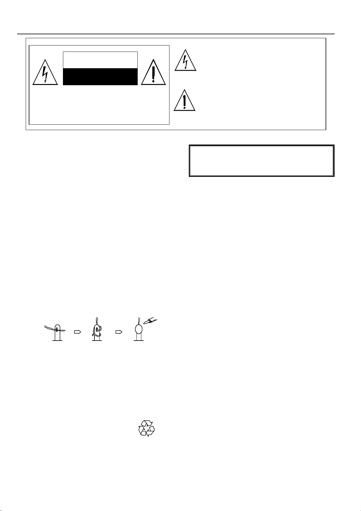
CAUTION
RISK OF ELECTRIC SHOCK
DO NOT OPEN
The lightning flash with arrowhead symbol,
within an equilateral triangle, is intended to alert
the user to the presence of uninsulated “ dangerous
voltage” within the product’ s enclosure that may
be of sufficient magnitude to constitute a risk of
electric shock to persons.
CAUTION: TO REDUCE THE RISK OF ELECTRIC
SHOCK, DO NOT REMOVE COVER (OR BACK). NO
USER-SERVICEABLE PARTS INSIDE. REFER
SERVICING TO QUALIFIED SERVICE PERSONNEL
ONLY.
PRECAUTIONS DURING SERVICING
1. In addition to safety, other parts and assemblies are
specified for conformance with such regulations as
those applying to spurious radiation. These must
also be replaced only with specified replacements.
Examples: RF converters, tuner units, antenna
selection switches, RF cables, noise-blocking
capacitors, noise-blocking filters, etc.
2. Use specified internal Wiring. Note especially:
1) Wires covered with PVC tubing
2) Double insulated wires
3) High voltage leads
3. Use specified insulating materials for hazardous
live parts. Note especially:
1) Insulating Tape
2) PVC tubing
3) Spacers (insulating barriers)
4) Insulating sheets for transistors
5) Plastic screws for fixing micro switches
4. When replacing AC primary side components
(transformers, power cords, noise blocking
capacitors, etc.), wrap ends of wires securely about
the terminals before soldering.
5. Make sure that wires do not contact heat generating
parts (heat sinks, oxide metal film resistors, fusible
resistors, etc.)
6. Check if replaced wires do not contact sharply edged
or pointed parts.
7. Make sure that foreign objects (screws, solder
droplets, etc.) do not remain inside the set.
MAKE YOUR CONTRIBUTION TO PROTECT THE
ENVIRONMENT
Used batteries with the ISO symbol
for recycling as well as small
accumulators (rechargeable batteries), mini-batteries
(cells) and starter batteries should not be thrown
into the garbage can.
Please leave them at an appropriate depot.
The exclamation point within an equilateral
triangle is intended to alert the user to the
presence of important operating and maintenance
(s erv ici ng) in str uct io ns in the li ter atu re
accompanying the appliance.
WARNING:
Before servicing this TV receiver, read the X-RAY
RADIATION PRECAUTION, SAFETY INSTRUCTION
and PRODUCT SAFETY NOTICE.
X-RAY RADIATION PRECAUTION
1. Excessively high can produce potentially hazardous
X-RAY RADIATION. To avoid such hazards, the high
voltage must not exceed the specified limit. The
normal value of the high voltage of this TV receiver
is 27 KV at zero bean current (minimum brightness).
The high voltage must not exceed 30 KV under any
circumstances. Each time when a receiver requires
servicing, the high voltage should be checked. The
reading of the high voltage is recommended to be
recorded as a part of the service record, It is
important to use an accurate and reliable high
voltage meter.
2. The only source of X-RAY RADIATION in this TV
receiver is the picture tube. For continued X-RAY
RADIATION protection, the replacement tube must be
exactly the same type as specified in the parts list.
3. Some parts in this TV receiver have special safety
related characteristics for X-RADIATION protection.
For continued safety, the parts replacement should
be under taken only after referring the PRODUCT
SAFETY NOTICE.
SAFETY INSTRUCTION
The service should not be attempted by anyone
unfamiliar with the necessary instructions on this TV
receiver. The following are the necessary instructions
to be observed before servicing.
1. An isolation transformer should be connected in the
power line between the receiver and the AC line
when a service is performed on the primary of the
converter transformer of the set.
2. Comply with all caution and safety related provided
on the back of the cabinet, inside the cabinet, on the
chassis or picture tube.
3. To avoid a shock hazard, always discharge the
picture tube's anode to the chassis ground before
removing the anode cap.
- 2 -
Page 3
4. Completely discharge the high potential voltage of the
2/100
picture tube before handling. The picture tube is a
vacuum and if broken, the glass will explode.
5. When replacing a MAIN PCB in the cabinet, always
be certain that all protective are installed properly
such as control knobs, adjustment covers or shields,
barriers, isolation resistor networks etc.
6. When servicing is required, observe the original lead
dressing. Extra precaution should be given to assure
correct lead dressing in the high voltage area.
7. Keep wires away from high voltage or high tempera
ture components.
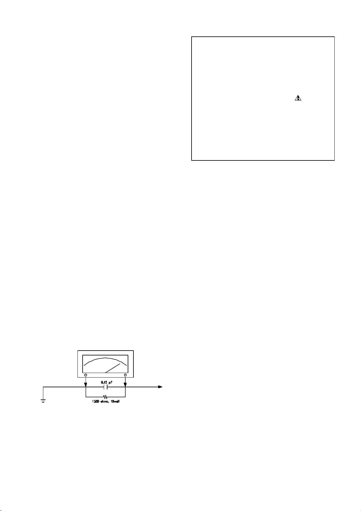
8. Before returning the set to the customer, always
perform an AC leakage current check on the exposed
metallic parts of the cabinet, such as antennas,
terminals, screwheads, metal overlay, control shafts,
etc., to be sure the set is safe to operate without
danger of electrical shock. Plug the AC line cord
directly to the AC outlet (do not use a line isolation
transformer during this check). Use an AC voltmeter
having 5K ohms volt sensitivity or more in the
following manner.
Connect a 1.5K ohm 10 watt resistor paralleled by a
0.15µF AC type capacitor, between a good earth
ground (water pipe, conductor etc.,) and the exposed
metallic parts, one at a time.
Measure the AC voltage across the combination of
the 1.5K ohm resistor and 0.15 uF capacitor. Reverse
the AC plug at the AC outlet and repeat the AC
voltage measurements for each exposed metallic
part.
The measured voltage must not exceed 0.3V RMS.
This corresponds to 0.5mA AC. Any value exceeding
this limit constitutes a potential shock hazard and
must be corrected immediately.
The resistance measurement should be done
between accessible exposed metal parts and power
cord plug prongs with the power switch "ON". The
resistance should be more than 6M ohms.
PRODUCT SAFETY NOTICE
Many electrical and mechanical parts in this TV
receiver have special safety-related characteristics.
These characteristics are offer passed unnoticed by
visual spection and the protection afforded by them
cannot necessarily be obtained by using replacement
components rates for a higher voltage, wattage, etc.
The replacement parts which have these special
safety characteristics are identified by marks on
the schematic diagram and on the parts list.
Before replacing any of these components, read the
parts list in this manual carefully. The use of
substitute replacement parts which do not have the
same safety characteristics as specified in the parts
list may create shock, fire, X-RAY RADIATION or
other hazards.
Good earth ground
such as the water
pipe, conductor,
etc.
AC Leakage Current Check
AC VOLTMETER
Place this probe
on e a c h e xposed met al li c
part
- 3 -
Page 4
KAWA ELECTRONIC RESEARCH & DEVELOPMENT CENTRE
Reference No : LCT2701TD
Product Specification
1.1 VIDEO SECTION
Display size 27”/16:9
Display Resolution 1366 X 768
Pixel Pitch
Peak Brightness 550(nits)
Contract Ratio 1000:1, Typical (1/100 White Window, Dark Room)
View Angle Hor. And Vert. 170 degree
Color Deeps 16.7M Color (R / G/ B each 256 Scales)
PC Resolution Supporting VGA, SVGA, XGA,WXGA
HDTV Compatible 480i / 480p / 720p / 1080i
Progressive Scanning Yes
Film Mode Pull Down Yes
“GAMMA” Correction Yes
Color Temperature Control Yes
Comb Filter Yes
Second De-interlace for Sub picture No
Wide Mode
TV System NTSC M
Dual Tuner System No
AV Input Color System PAL /NTSC
PIP Basic mode (video on graphic mode,resolution 1024×768)
1.2 AUDIO SECTION
CHIMEI V270B1-L01
MK8205
USA
0.1460mm×0.4365mm
Normal, Full, Wide 1, Wide 2, Wide 3, 4:3, No scale and
Panoramic.
Audio Output Power 6W×2 Max.(8 ohm)
Sound Effect Spatial Effect and Surround
Tone Control Yes
1.3 Input Terminals
(3.5mm Phone Type) x 1
1.4 Output Terminals Audio Output (RCA ; L&R Type) ×1
1.5 Others
Closed Caption / V-Chip Yes
Teletext No
OSD Language English, FranÇais, Español
D-Sub 15 Pin Type(
D-Sub 9 Pin (RS-232)
RF (F-type Input) ×1
Component Video-YPbPr ×1 RCA Terminals
S-Video Input (Mini Din 4Pin) ×1
Video Input RCA Terminals
Stereo Audio Input for YPbPr x 1
Analog-RGB Input ) ×1
3/100
Page 5
KAWA ELECTRONIC RESEARCH & DEVELOPMENT CENTRE
Reference No : LCT2701TD
Stereo Decode
Power Rating AC 120 V, 60Hz
Power Consumption 200W
1.6 Support the Signal Mode
This machine can support the different from VGA signal mode in 7 kinds
No Resolution
1) 640×480 31.50 60.00 25.18
2) 640×480 37.86 72.81 31.50
3) 800×600 35.16 36.00
4) 800×600 37.90 60.32 40.00
5) 800×600 46.90 75.00 49.50
6) 800×600 48.08 72.19 50.00
7) 1024×768 48.40 60.00 65.00
MTS with SAP
Horizontal
Frequency(Hz)
Vertical
Frequency(KHz)
Dot Clock
Frequency(MHz)
56.25
1.7 HDTV Mode (YPbPr)
No Resolution
1) 15.734 59.94 13.50
2)
3)
4)
480i
480p(720×480)
720p(1280×720)
1080i(1920×1080)
Horizontal
Frequency(KHz)
31.468 27.00
45.00 74.25
33.75 74.25
Vertical
Frequency(Hz)
59.94
60.00
60.00
Dot Clock
Frequency(MHz)
4/100
Page 6
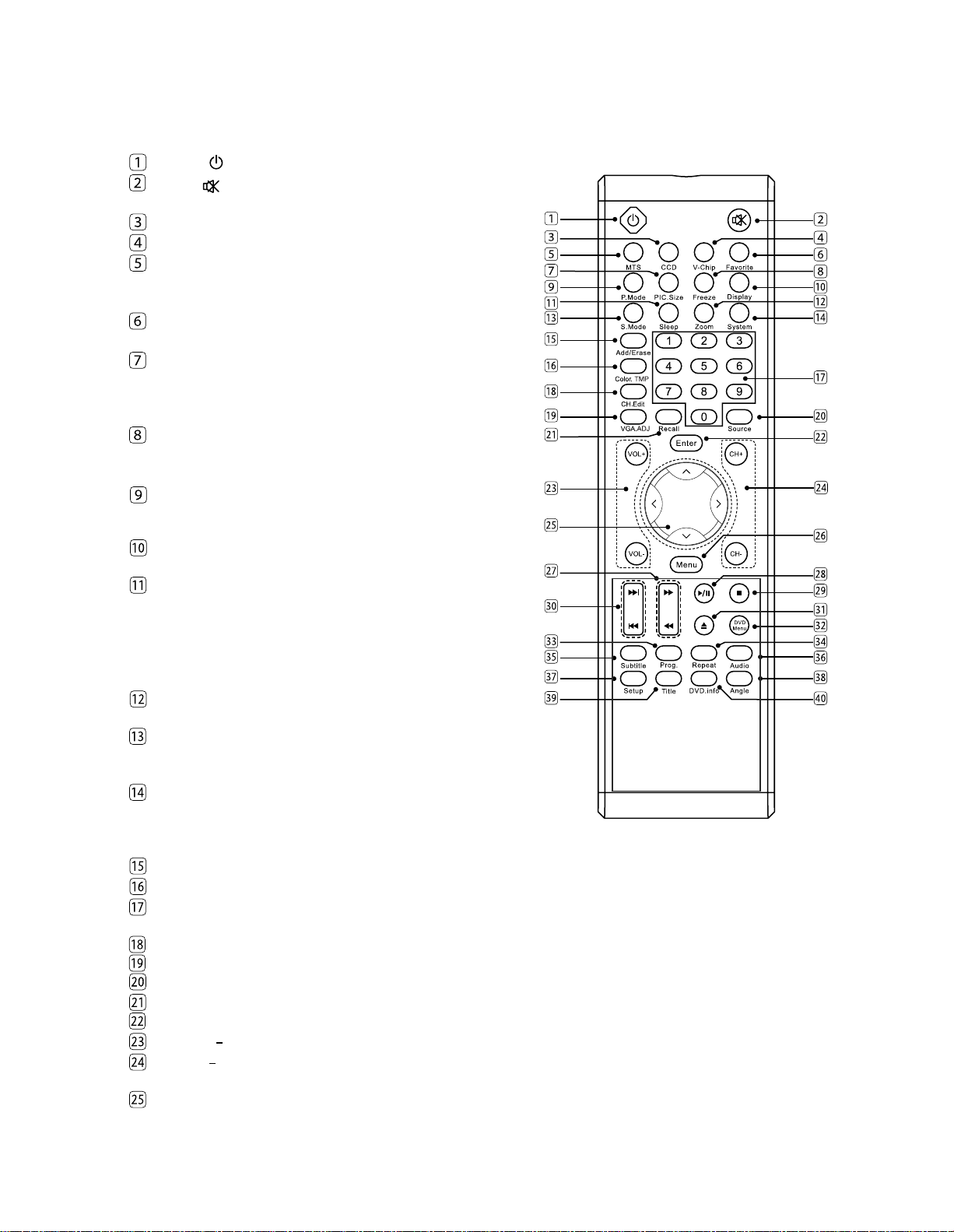
1.8 Remote Control
Power ( ): Press to turn on and off.
Mute ( ): Press to mute the sound. Press
again or press VOL+/- to restore the sound.
CCD: Press to select the Closed Caption mode.
V-Chip: Press to select the child protect mode.
MTS: Press repeatedly to cycle through
channel TV sound (MTS) options: Mono, Stereo
and SAP (Second Audio Program).
Favorite: Press repeatedly to cycle through the
favorite channel list.
PIC.Size: Press repeatedly to cycle through the
picture size that best corresponds your viewing
requirements: Normal, Full, Wide1, Wide2,
Wide3, 4:3, No scale, Panoramic and Normal.
Freeze: Press to freeze the picture, press again
to restore the picture. (This button is not available
for VGA mode.).
P.Mode: Press repeatedly to cycle through the
picture mode: Hi-Bright, User, Dark, Normal
and Vivid.
Display: Press to display the channel information
and it disappear after 3 seconds.
Sleep: Press repeatedly until it displays the time
in minutes (5 Min, 10 Min, 15 Min, 30 Min, 60
Min, 90 Min, 120 Min and, OFF) that you want
the TV to remain on before shutting off. To
cancel sleep time, press Sleep button repeatedly
until sleep OFF appears.
Zoom: Press to zoom the image. (This button is not
avialable for VGA mode.)
S.Mode: Press repeatedly to cycle through the
sound mode: Normal, News, Cinema, Flat and
User.
System: Press repeatedly to cycle through the
system options: AUTO and NTSC3.58.
(This button is activate for AV, S-Video input
source.)
Add/Erase: Press to add or delete favorite channel.
Color TMP: Press to select the color temperature.
0~9 Number Buttons: In TV mode, press 0~9 to
seconds. In DVD mode, press 0~9 to input the items.
CH Edit: Press to edit channel name.
VGA ADJ: Press to auto adjust VGA position.
Source: Press to select the signal source, such as TV, AV, S-Video, Component, DVD, or VGA.
Recall: Press to return previous channel.
Enter:
VOL+/: Press to adjust the volume.
CH+/ : Press to scan through channels. To scan quickly through channels, press and hold
To select an item, press Enter to confirm.
down either channels.
<,∧,∨,>
: Press<,∧,∨,>to move the on-screen cursor.
the Multi-
select a channel; the channel changes
after 2
5/100
Page 7

Menu: Press to enter on-screen
press again to exit.
DVD Menu: Press to return DVD disc menu.
Repeat: Press repeatedly to cycle
Subtitle: Press to select desired DVD subtitle.
, : Press
forward.
: Press to play or pause the DVD disc.
: Press to stop playing the disc.
, : Press to skip the backward or
forward.
: Press to open or close the disc tray.
Prog: Press to display the program menu. Press
it again to exit.
options: CHAPTER, TITLE, ALL and nothing.
to search the backward
setup menu,
through the
Audio: Press to select desired audio track.
Setup: Press to display a menu. Press it again
to exit menu.
Angle: Press to select desired viewing angle of
the Video (disc feature).
Title: Press to display to DVD disc title.
DVD Info: Press to display DVD information.
Note: Press CH+/-on the remote control can turn on
TV set from last preview mode.
6/100
Page 8
KAWA ELECTRONIC RESEARCH & DEVELOPMENT CENTRE
Reference No : LCT2701TD
Technical Data
TV AC 120V , 60Hz 1. Power supply
Remote control Battery 3V (UM-3/R6P/AA×2)
RF input NTSC M 2. TV system
Video input PAL/NTSC 3.58/NTSC 4.43
3. Receiving channels
TV
VHF-L : 2~6CH
VHF-H : 7~13CH
UHF : 14~69CH
CATV
4. Intermediate
frequencies
5. Sca nni ng ori z on t al (Hz ) 15625/15750
6. AC plug UL Plug
7. Panel V270B1-L01
8. Speaker Internal 8 ohm 6W (max) ×2
9. Operating
temperature
Accept picture/sound
10. Operating relative
humidity
Accept picture/sound
11. Electrical &
optical
specification
12. Circuit diagram
drawing No.
13. Cabinet
14. Cabinet color
15. Packing 1 set per
16. Container stuffing
method
17. Dimension (mm) LCD-TV
(No packing)
Remote control unit
18. Net weight LCD-TV 13.9Kg (with Stand) approx
Remote control 70g (approx)
Picture
H
Ver tic al ( Hz) 50/60
Fulfill all specifications
reproduction
Fulfill all specifications 45% ~ 75%
reproduction
See the attachment 1.
RD/05/P/LC26HAB/CSI/02 REV: 01
1~125CH
45.75MHz
15 C ~ 30 C
5 C ~ 33 C
20% ~ 80%
LCT2701TD
698(W) x 513(H) x 99(D)mm (w/o Stand)
698(W) x 554(H) x 250(D)mm (with Stand)
183(L) x 53(W) x 28(T)mm
19. Cell Defect Subject to Panel supplier specification
7/100
Page 9
KAWA ELECTRONIC RESEARCH & DEVELOPMENT CENTRE
8/100
Reference No : LCT3201TD
Attachment 1:Electrical & Optical Specification
No. Items Instruction Typical Limit Unit
1 Video sensitivity For 30dB S/N 44 ≤51 dBuV
2 FM sound sensitivity For 30dB S/N 21 ≤35 dBuV
3 Color sensitivity For RF transmission 37 ≤40 dBuV
4 CCD sensitivity
5 Minimum NICAM threshold Without crackline noise N/A N/A dBuV
6 Stereo Channel Separation BTSC. 18 ≥15 dB
TV screen refreshes 40 times
number of mistakes≤8
43 ≤50 dBuV
AGC static characteristic
7
8 Selectivity Adjacent sound carrier 30 ≥28
Below adjacent sound carrier 30 ≥30 dB
Adjacent picture carrier 45 ≥40
Up adjacent picture carrier 40 ≥30
9 IF rejection 55 ≥45 dB
10 Image rejection VHF 57 ≥45 dB
UHF 55 ≥40
11 AFT pull-in range ±1.0 ≥⏐±1.0⏐ MHz
12 Chroma sync pull-in range ±500 ≥⏐±200⏐ Hz
13 Color killer function -11 ≤-10 dB
14 Resolution
Video
Accept. Picture/Sound repr. 90
RF
Vertical
Horizontal
Vertical 400 ≥400 Lines
PAL 300 ≥300 Lines Horizontal
NTSC 260 ≥240 Lines
PAL 410 ≥400 Lines
NTSC 320 ≥300 Lines
450 ≥450 Lines
≥90
dBuV
White
Coordination
16 View
Angle(Lo/3)
17 Overscan Cross hatch signal 96 94~98 %
Horizontal
Vertical
XW 0.295 0.295±0.02 15 Color
Y
W
Full Pattern
0.300 0.300±0.02
170
≥170
Degree
18 Picture position In all direction ±2 ≤⏐±3⏐ mm
19 H sync pull-in range ±400 ≥⏐±200⏐ Hz
20 V sync pull-in range 6 ≥6 Hz
21 Audio frequency response ±3dB ref. to 1KHz 0.15~12 0.2~12 KHz
Page 10
KAWA ELECTRONIC RESEARCH & DEVELOPMENT CENTRE
9/100
Reference No : LCT3201TD
22
Max Audio Output Power 7×2 ≥5.0×2 W
23 Audio output power
10% THD
24 THD Po=0.5W 0.5 ≤3 %
25 Signal to buzz ratio coeighting 50 ≥30 dB
26 Minimum volume hum coeighting 6 ≤10 mVrms
27 Maximum woofer output power N/A N/A W
28 Woofer audio frequency
response
29 Tone low frequency 100Hz ref. to 1KHz
30 Tone high frequency 10KHz ref. to 1KHz
31 Balance Center 0 ≤⏐±2⏐
Max. 3 >2 dB
Min. -35 ≤-30
32 Video input level 1.0 1±0.3 Vpp
1KHz 10% THD 6×2
±3dB ref. to 15Hz AV
mode
AV mode
AV mode
N/A N/A Hz
±8 ≥⏐±3⏐ dB
±8 ≥⏐±3⏐ dB
≥4.0×2 W
33 Audio input level*(1) 1.0 * 0.5±0.3 Vrms
34 Video output level N/A N/A Vrms
35 Audio output level*(2) 0.3 * 0.5±0.3 Vrms
36 AV Audio input max. level 2 ≤2 Vrms
37 AV Audio output L/R
Separation
39 IR receiving distance 0 Degree 7 ≥6 m
IR receiving
angle
41 Dielectric strength DC 3KV 1min. 5 ≤10 mArms
42 The vibration noise from
electromagnetic devices in LCD-
TV set
left/right 60 ≥45 Degree40
Up/down
35 ≥30 dB
Operating 200 ≤200 W 38 Power consumpution
Stand by 3 ≤5 W
5m
The distance between
the tester and the
LCD-TV set is four
times as many as the
screen height
20 ≥15 Degree
No obvious vibration noise can be
heard
Page 11
KAWA ELECTRONIC RESEARCH & DEVELOPMENT CENTRE
10/100
Reference No : LCT3201TD
Test Condition
All tests shall be performed under the following conditions unless otherwise specified
1 Picture Modulation 87.5%
2 Sound Modulation
3 Picture to Sound Ratio 10dB
4 Sound Artificial Load
Resistor
Video signal
5
6 Audio signal 1KHz sine wave 0.5Vrms
7 Other conditions:
A. Switch LCD-TV on and let it warm up for more than 30 minutes.
Viewing distance: 3H (H: Panel High) in front of LCD, about 2M.
Ambient light: ≤0.1 cd/ m
B. Brightness, Contrast, Saturation, Tint, sharpness set at normal.
C. Connect RMS volt meter to speaker terminals and adjust the LCD volume to get 500mW RMS
power at each terminals.
D. With image sticking protection of LCD module. The luminance will descend by time on a same
still screen and rapidly go down in 5 minutes, when measuring the color tracking and luminance
of a same still screen, be sure to accomplish the measurement in one minute to ensure its
accuracy.
E. Due to the structure of LCD module. The extra-high-bright same screen should not hold over 5
minutes for fear of branding on the panel.
F. RF test point: Video output.
27KHz Dev. For DK/I/BG
15KHz Dev. For M/N
8 ohm
Stair and Special
2
8 Note:
*(1) Now this project cannot fit the limited spec. the typical audio input level is 1.0 Vrms,
*(2) The audio out level is controlled by the volume level, the range is from 0 to 0.5Vrms.
Page 12
DVD player's spec. For LCD-TV Combo
e
t
Division Section Remarks
name AKAI
Marketing Area( setup default language)
General
DVD Module
Playback Playable Media Type Playable Disc Type: DVD, CD,
Disc Type Playable Disc Type DVD(Single/ Dual layer, Double sided), CD
Video Video output signal NTSC
Audio Audio DAC
Playback Fast forward/backward x2,x4,x8,x16,x32
Features Slow motion forward x1/2,x1/4,x1/8,x1/16
Display Graphical user interfac
user OSD Language 3 (ENG is base ,SPA and French)
operation Subtitle Present
Front Panel VFD/ LED x
Rear Panel Composite Video output x
Power supply +5v,+3.3v
Power Consumption 15W
Manufactruer of Loader mechanism Foryou DL06-LS
Opitical Pick UP
Chipset used MTK 1389FE
Disc Size 8cm/12cm
Regional code
NTSC/ PAL Disc playback O/O
Video DAC 27MHz/ 10bit
Dynamic range Present
Dolby digital decoder Present
DTS decoder optional
SRS + TruSurround for 2 channel Not present
3D Virtual surround for 2 channel Not present
Slow motion backward optional
Still picture Present
Frame by frame forward/reverse Forward only (Step function)
Skip forward/reverse Present
Repeat function Present
DVD closed caption Present
Transition Effect for picture CD Not present
Rotation of picture for picture CDs Present
Last Memory Present
Screen saver Present
Resume play Present
Program function Present
PBC ON/OFF Default on PCB
Parental lock Passward : 0000
Picture mode selector 16:9, 4:3 LB, 4:3 PS(4:3 PS as default)
Intro scan Not present
Digest in VCD Present, only for PIC CD
Time search Present
Multi angle Present
Selectable audio language streams Present
kalaoke function x
No. of keys 3(Open/Close, Play, Stop)
Component Video output x
Progressive scan output (480P) Present
2 channel audio output Present
Coaxial audio output Present
USA
Sanyo HD-62/65
Regional 1
48Khz/ 96KHz/24-bit:selectable
Not presen
11/100
Page 13
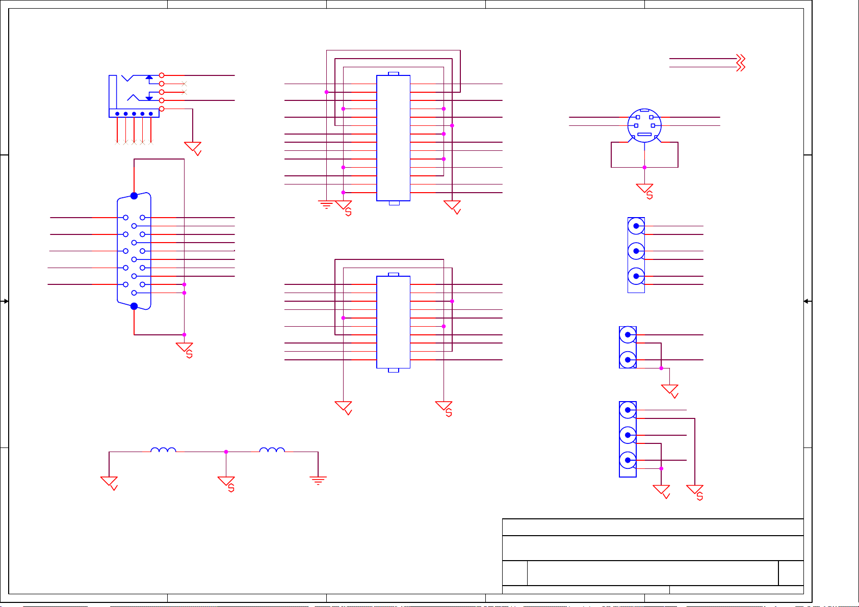
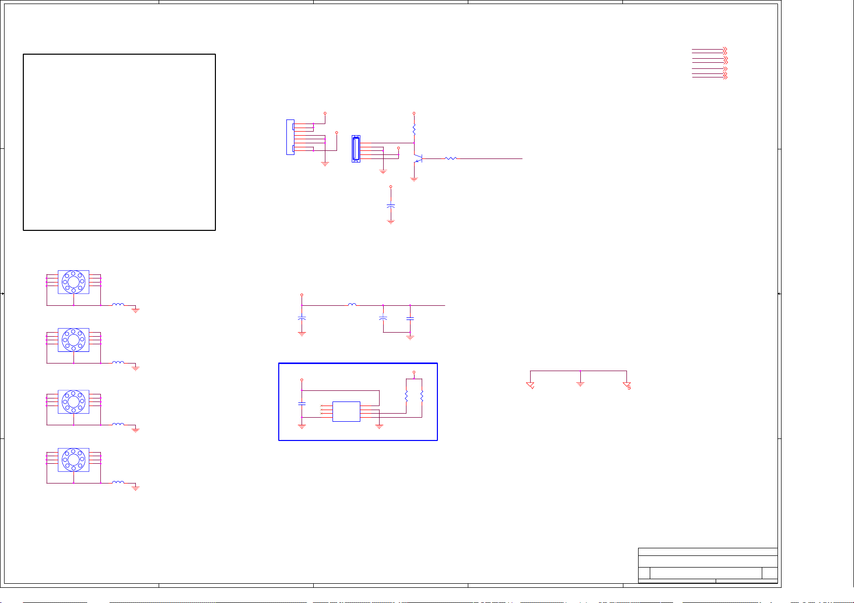
LCD COMBO Connection
L
R
PWM
On/Off
PWM
+24V
+24V
+5V +5V STB
+5V IR2 +12V
Y/Pb/Pr (480p)
L/R
Turner+Amp
IR1
Key Board
Key Board
Main board
DVD
LVDS×1
Panel
Backlight
Power board
12/100
Page 14
5
4
3
2
1
Dimming
BL_ON/OFF
D D
9
9
8
8
7
7
6
6
H1
Dimming
BL_ON/OFF
HOLE/GND
2
3
4
5
Inverter_PWR
2
3
4
5
CE1
+
470uF/50v
PANEL INVERTER POWER
CE2
+
470uF/50v
C1
0.1uF
C2
0.1uF
Inverter_PWR
PWR_GND
1
1
FB5
120R
Inverter_PWR
J1
1
2
3
4
HOLE/GND
H2
C C
9
9
8
8
7
7
6
6
1
1
2
2
3
3
4
4
5
5
Dimming
BL_ON/OFF
FB6
120R
5
6
7
8
R. ANGLE
9
10
11
12
1
12x1 W/HOUSING R.A
J2
8x1 W/HOUSING
SIP6\2.54
1
INVERTER_PWR
2
3
4
PWR_GND
5
6
SIP12\2
J3
C3
HOLE/GND
H3
9
9
B B
8
8
7
7
6
6
2
2
3
3
4
4
5
5
0.1uF
1
1
FB7
120R
PWR_GND
FB1
120R
FB2
120R
1206
HOLE/GND
H4
9
9
8
8
7
7
6
A A
6
1
1
2
2
3
3
4
4
5
5
FB8
120R
1206
1
2
3
4
5
6
7
R. ANGLE
8
9
10
10x1 W/HOUSING R.A.
SIP10\2
Title
<Title>
HOLE/GND
H5
9
9
8
8
7
7
6
6
2
2
3
3
4
4
5
5
1
1
FB9
120R
Size Document Number Re v
<Doc> <RevCode>
A
5
4
3
13/100
Date: Sheet
2
of
12Wednesday, August 24, 2005
1
Page 15
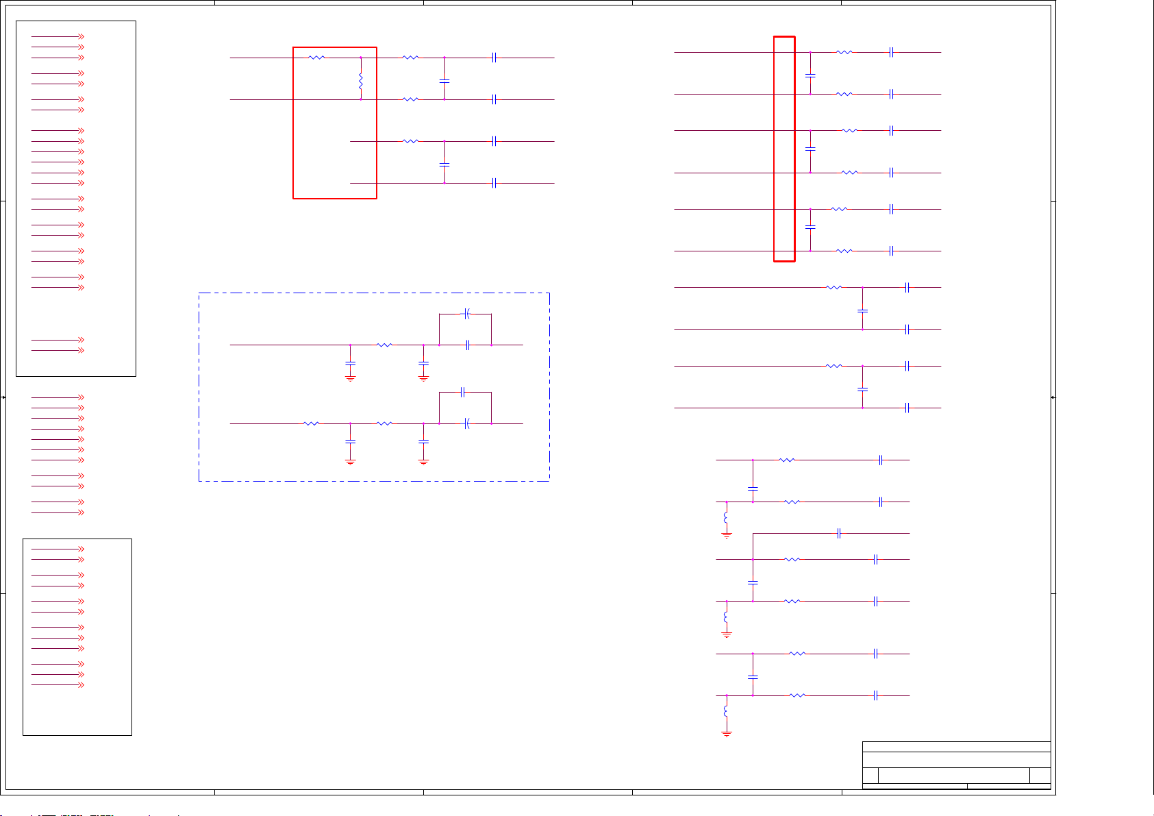
5
4
3
2
1
J5
R
1
D D
J4
VGA AUDIO
PHONEJACK/DIP
2
3
L
4
G
K1K2K3K4K5
J7
1617
DSUB15/DIP/F
VGA_R
VGA_L
Dimming BL_ON/OFF
RSTXD
VGA_R
RED
RED_GND
BLUE
BLU_GND
VGA_SDA
10
12
14
16
18
20
22
24
2
4
6
8
1
3
5
7
9
RSRXD
VGA_L
11
13
15
17
19
21
23
2526
2728
GREEN
GRN_GND
VGA_PWR
HSYNC#VSYNC#
VGA_SCL
SC_IN
SC_GND1
J6
CON\SVHS
2
1
7
6
Dimming
BL_ON/OFF
SY_IN
3
SY_GND1
4
5
Dimming
BL_ON/OFF
DB15
RSRXD
C C
VGA_SDA
11
12
1
6
2
7
3
8
4
9
5
VSYNC#
VGA_SCL
13
14
15
10
RED
RED_GND
GREEN
GRN_GND
BLUEHSYNC#
BLU_GND
RSTXD
VGA_PWR
Y1_INB
CR1_INB
CR1_GNDB
AV1_IN
SC_IN
SC_GND1
SY_IN
B B
PC CONNECTOR
DIP14X2/P2.54/R2
J9
2
4
6
8
10
12
14
16
18
20
1
3
5
7
9
11
13
15
17
19
VIDEO CONNECTOR
CB1_INB
CB1_GNDBY1_GNDB
YPBPR1/L
YPBPR1/R
AV_L
AV_R
SY_GND1
J8
RCA1X3
RCA3/6P/DIP
J10
1
2
3
RCA1X2
4
RCA2/4P/DIP
Y1_INB
1
Y1_GNDB
2
CB1_INB
3
CB1_GNDB
4
CR1_INB
5
CR1_GNDB
6
YPBPR1/L
YPBPR1/R
DIP10X2/P2.54/R2
J11
AV1_IN
1
2
FB3
120R
FB4
120R
AV_L
3
4
AV_R
5
6
RCA1X3
RCA3/6P/DIP
DIGITAL GNDAUIO IN/OUT GND ANALOG INPUT GND
A A
Title
<Title>
Size Document Number Re v
<Doc> <RevCode>
A
of
5
4
3
14/100
Date: Sheet
2
22Wednesday, August 24, 2005
1
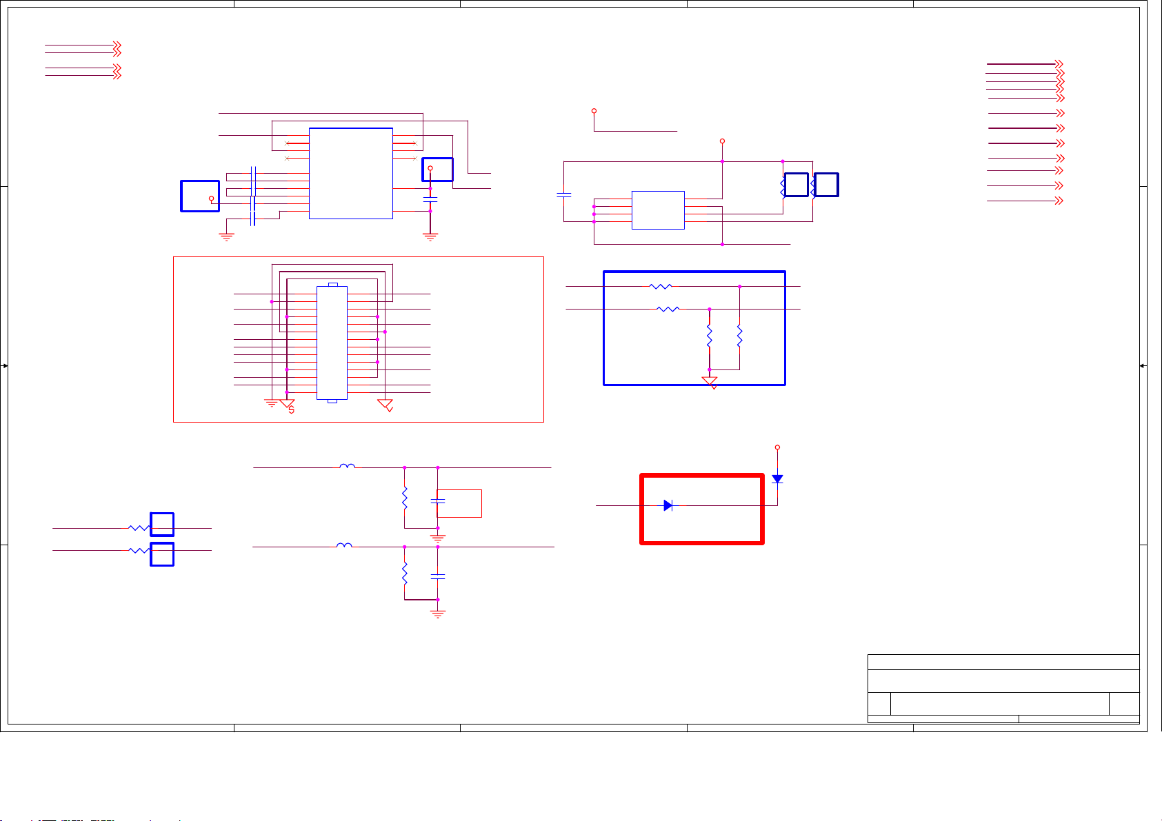
Page 16
A
B
C
D
E
AN0
AP0
AN1
C1
0.1uF
AP1
AN2
AP2
CLK1CLK1+
AN3
AP3
AN4
AP4
AN5
AP5
AN6
AP6
CLK2CLK2+
AN7
AP7
C2
0.1uF
4 4
3 3
VSYNC
HSYNC
R
G
B
CLK1+
CLK1CLK2+
CLK2-
ORO1
AP[0..7]
AN[0..7]
+12V
VSYNC 3
HSYNC 3
R3
G3
B3
CLK1+ 3
CLK1- 3
CLK2+ 3
CLK2- 3
ORO1 3
AP[0..7] 3
AN[0..7] 3
+12V 1
+12V
VCC
Optinal for 12V pannel.Added by bin_wang 16/7/05
FB2
FB1
75R/NC
75R
0805
ORO1 High :LVDSVDD POWER OFF
ORO1 LOW :LVDSVDD POWER ON
0805
Add LVDS VCC control by Zheng_guo 15/9/05.
ORO1
R211
2k
F1
CE1
4A/32v
1206
+
330uF/25v
C330UF25V/D8H14
+12V
R210
R209
22k
22k
Q10
1
2N3904
2 3
Q9
1
S1
D1
2
G1
D1
3
S2
D2
4 5
G2 D2
IR7314
SOP8
LVDSVDD
8
7
6
+
CE2
220uF/16v
CE3
220uF/16v
+
J1
1
2
3
4
5
6
7
8
9
10
11
12
13
14
15
16
17
18
19
20
21
22
23
24
25
26
27
28
29
30
FI-SE30P-HF
LVDS/30P/P1.25/S
R
75 1%
G
75 1%
B
75 1%
CRT OUT
R1
GND
R2
GND
R3
GND
R
G
B
HSYNC
VSYNC
RGB OUTPUT FOR DEBUGGING
VS
HS
ORO3
PWM0
Dimming
2 2
1 1
A
BL_ON/OFF
ORO3 3
PWM0 3
Dimming 6
BL_ON/OFF 6
VCC
R4 0
R7
PWM0
4.7k
ORO3 High :PANEL BACKLIGHT POWER OFF
ORO3 LOW :PANEL BACKLIGHT POWER ON
R5
10k
R6
Q1
1
2N3904
SOT23
2 3
100k
Back Light circuit
ORO3
B
C3
0.1uF
FOR CHI-MEI INVERTER
CONNECTOR
Dimming
VCC
R8
10k
R9
4.7k
BL_ON/OFF
Q2
1
2N3904
SOT23
2 3
Title
MiCO LCD TV - MediaTek MT8203 Solution
Size Doc Number Rev
C
C
D
Date: Sheet of
LVDS/CRT/BACKLIGHT CONTROL
E
MiCO Confidential
110Wednesday, September 28, 2005
V0.1
15/100
Page 17
A
B
C
D
E
VGASOG
RED+
RED-
GREEN+
GREEN-
BLUE+
4 4
BLUE-
CB+
CB-
CR+
CR-
Y+
Y-
SY+
SY-
SC+
SC-
CVBS0+
CVBS0-
CVBS1+
CVBS1-
3 3
MPX1
MPX2
Y
Y_GND
CB
CB_GND
CR
CR_GND
SOY
SY
SY_GND
2 2
SC
SC_GND
CVBS0
CVBS0_GND
CVBS1
CVBS1_GND
SIF1_OUT
AF1_OUT
RED
GREEN
BLUE
RED_GND
GRN_GND
BLU_GND
1 1
VGASOG 3
RED+ 3
RED- 3
GREEN+ 3
GREEN- 3
BLUE+ 3
BLUE- 3
CB+ 3
CB- 3
CR+ 3
CR- 3
Y+ 3
Y- 3
SY+ 3
SY- 3
SC+ 3
SC- 3
CVBS0+ 3
CVBS0- 3
CVBS1+ 3
CVBS1- 3
MPX1 3
MPX2 3
OUTPUT
Y7
Y_GND 7
CB 7
CB_GND 7
CR 7
CR_GND 7
SOY 3,7
SY 7
SY_GND 7
SC 7
SC_GND 7
CVBS0 7
CVBS0_GND 7
CVBS1 7
CVBS1_GND 7
SIF1_OUT 7
AF1_OUT 7
RED 6
GREEN 6
BLUE 6
RED_GND 6
GRN_GND 6
BLU_GND 6
INPUT
R12 18
CVBS0_GND
Change.
FROM Tuner
SIF1_OUT
AF Path
R40 39k
AF1_OUT
R15
56
CVBS1
CVBS1_GND
R35 8.2K
C23
15pF/NC
R41 39k
C29
15pF
R13
22
R17
0
R21
22
C24
15pF/NC
C30
15pF
C7
330pF
C13
330pF
CE4
+
47uF/16v /NC
C22
47nF
C26
47nF/NC
CE5
+
47uF/16v
C5
C9
C11
C15
CVBS0+CVBS0
47nF
CVBS0-
47nF
CVBS1+
47nF
CVBS1-
47nF
MPX1
MPX2
Y
Y_GND
CB
CB_GND
CR
CR_GND
SY
SY_GND
SC
SC_GND
Change.
ATTENTION:WHEN PCB LAYOUT,MUST NEAR VGA INPUT PORT! BIN_WANG. 16/7/05
RED
RED_GND
GREEN
GRN_GND
BLUE
BLU_GND
R42 68
C32
5pF
R44 100
FB4
70R
R46 68
C36
5pF
R48 100
FB6
70R
R49 68
C39
5pF
R51 100
FB8
70R
R11
100
C6
15pF
R16
100
C12
15pF
R27
100
C17
15pF
R29
100
R31
22
R37
22
C34
4.7nF
MODIFIED BY BIN_WANG 16/7/05.
A
B
C
D
C4
47nF
C8
47nF
C10
R19
100
R24
100
47nF
C14
47nF
C16
47nF
C18
47nF
C20
330pF
C27
330pF
C31
47nF
C33
47nF
VGASOG
C35
GREEN+
47nF
C37
GREEN-
47nF
C38
47nF
C40
47nF
Title
MiCO LCD TV - MediaTek MT8203 Solution
Size Doc Number Rev
C
Date: Sheet of
RED+
RED-
BLUE+
BLUE-
Y+
Y-
CB+
CB-
CR+
CR-
C19
SY+
47nF
C21
SY-
47nF
C25
SC+
47nF
C28
SC-
47nF
MiCO Confidential
AV IN
E
210Thursday, September 15, 2005
V0.1
16/100
Page 18
A
B
C
D
E
TXD
RXD
Dimming
BL_ON/OFF
4 4
3 3
2 2
VGASDA
VGASCL
TXD 3
RXD 3
Dimming 9
BL_ON/OFF 9
R59 33
R60 33
VGA_SDA
VGA_SCL
RSRXD
RSTXD
C41 0.1uF
C42 0.1uF
+5V
C44 0.1uF
C46 0.1uF
Dimming BL_ON/OFF
RSTXD
VGA_R
RED
RED_GND
BLUE
BLU_GND
VGA_SDA
U1
13
R1IN
8
R2IN
11
T1IN
10
T2IN
1
C+
3
C1-
4
C2+
5
C2-
2
V+
6
V-
MAX232A
2728
24
22
20
18
16
14
12
10
8
6
4
J2
2
HSYNC# HSYNC_VGA
2526
23
21
19
17
15
13
11
9
7
5
3
1
PC CONNECTOR
DIP14X2/P2.54/R1
FB9
70R
0603
FB10
70R
0603
R1OUT
R2OUT
T1OUT
T2OUT
VCC
GND
12
9
14
7
16
15
RSRXD
VGA_L
GREEN
GRN_GND
VGA_PWR
HSYNC#VSYNC#
VGA_SCL
R58
2.2k
R61
2.2k
+5V
C45
0.1uF
TXD
RXD
Modified by MICO.
VGAVSYNC#VSYNC#
C47
100pF
C48
5pF
VGA_PLUGPWR
VGA_PLUGPWR
C43
0.1uF
U2
1
NC
2
NC
3
NC
4 5
GND SDA
EEPROM 24C02
R54
VGA_R
R55 15K
VGA_L VGA_IN_L
VCC
WP
SCL
15K
D2
DIODE SMD
1N4148/SMD
VGA_PLUGPWR
8
7
6
VGA_PLUGPWRVGA_PWR
R56
75K
VGASCL
VGASDA
GND
R57
75K
VGA_IN_R
VCC
R52
4.7k
D1
DIODE SMD
1N4148/SMD
R53
4.7k
VGA_IN_L
VGA_IN_R
VGASDA
VGASCL
HSYNC_VGA
VGAVSYNC#
RED_GND
GRN_GND
BLU_GND
RED
GREEN
BLUE
VGA_IN_L 10
VGA_IN_R 10
VGASDA 3
VGASCL 3
HSYNC_VGA 3
VGAVSYNC# 3
RED_GND 8
GRN_GND 8
BLU_GND 8
RED 8
GREEN 8
BLUE 8
1 1
Title
MiCO LCD TV - MediaTek MT8203 Solution
Size Doc Number Rev
B
A
B
C
D
Date: Sheet of
VGA IN & PC AUDIO IN
MiCO Confidential
310Thursday, September 15, 2005
E
V0.1
17/100
Page 19
A
B
C
D
E
RN4
F_D[0..7]
F_A[0..21]
A_DQS[0..3]
A_RA[0..11]
A_BA[0..1]
A_DQM[0..1]
A_DQ[0..31]
A_CLK
A_CLK#
4 4
A_CKE
A_CS#
A_RAS#
A_CAS#
A_WE#
SDV25
VREF
IOWR#
IOCE#
F_OE#
F_D[0..7]
F_OE#
F_A[0..21]
3 3
2 2
1 1
F_D[0..7] 3
F_A[0..21] 3
A_DQS[0..3] 3
A_RA[0..11] 3
A_BA[0..1] 3
A_DQM[0..1] 3
A_DQ[0..31] 3
A_CLK 3
A_CLK# 3
A_CKE 3
A_CS# 3
A_RAS# 3
A_CAS# 3
A_WE# 3
SDV25 3
VREF 3
IOWR# 3
IOCE# 3
F_OE# 3
F_D[0..7] 3
F_OE# 3
F_A[0..21] 3
A_RA3
7 8
A_RA2
5 6
A_RA1
3 4
A_RA0
1 2
RN5
A_RA4
7 8
A_RA5
5 6
A_RA6
3 4
A_RA7
1 2
RN7
A_RA8
7 8
A_RA9
5 6
A_RA11
3 4
A_RA10
1 2
RN9
A_DQ0
7 8
A_DQ1
5 6
A_DQ2
3 4
A_DQ3
1 2
RN11
A_DQ4
7 8
A_DQ5
5 6
A_DQ6
3 4
A_DQ7
1 2
RN13
A_DQ8
7 8
A_DQ9
5 6
A_DQ10
3 4
A_DQ11
1 2
RN14
A_DQ12
7 8
A_DQ13
5 6
A_DQ14
3 4
A_DQ15
1 2
RN24
A_DQ16
7 8
A_DQ17
5 6
A_DQ18
3 4
A_DQ19
1 2
RN26
A_DQ20
7 8
A_DQ21
5 6
A_DQ22
3 4
A_DQ23
1 2
RN27
A_DQ24
7 8
A_DQ25
5 6
A_DQ26
3 4
A_DQ27
1 2
RN29
A_DQ28
7 8
A_DQ29
5 6
A_DQ30
3 4
A_DQ31
1 2
A_DQS0
A_DQS1
A_DQS2
A_DQS3
A_CS# D_CS#
A_RAS#
A_CAS#
A_WE#
R67 22
A_BA1
R68 22
A_BA0
A_DQM0
A_DQM1
A_CKE
A_CLK
A
R65 47
R66 47
R201 47
R202 47
R71 22
R206 22
R73 22 C77
R75 22
R77 22
22x4
22x4
22x4
47x4
47x4
47x4
47x4
47x4
47x4
47x4
47x4
RN16
7 8
5 6
3 4
1 2
22x4
D_RA3
D_RA2
D_RA1
D_RA0
D_RA4
D_RA5
D_RA6
D_RA7
D_RA8
D_RA9
D_RA11
D_RA10
D_DQ0
D_DQ1
D_DQ2
D_DQ3
D_DQ4
D_DQ5
D_DQ6
D_DQ7
D_DQ8
D_DQ9
D_DQ10
D_DQ11
D_DQ12
D_DQ13
D_DQ14
D_DQ15
D_DQ16
D_DQ17
D_DQ18
D_DQ19
D_DQ20
D_DQ21
D_DQ22
D_DQ23
D_DQ24
D_DQ25
D_DQ26
D_DQ27
D_DQ28
D_DQ29
D_DQ30
D_DQ31
D_DQS0
D_DQS1
D_DQS2
D_DQS3
D_RAS#
D_CAS#
D_WE#
D_BA1
D_BA0
D_DQM0
D_DQM1
D_CKE
D_CLK
D_CLK#A_CLK#
SDV25 SDV25
D_DQ0
D_DQ1
D_DQ2
D_DQ3
D_DQ4
D_DQ5
D_DQ6
D_DQ7
D_DQS0
D_DQM0
D_WE#
D_CAS#
D_RAS#
D_CS#
D_BA0
D_BA1
D_RA10
D_RA0
D_RA1
D_RA2
D_RA3
SDV25 SDV25
D_DQ16
D_DQ17
D_DQ18
D_DQ19
D_DQ20
D_DQ21
D_DQ22
D_DQ23
D_DQS2
D_DQM1
D_WE#
D_CAS#
D_RAS#
D_CS#
D_BA0
D_BA1
D_RA10
D_RA0
D_RA1
D_RA2
D_RA3
D1V25
D1V25
VREF
VREF
VREF
VREF
C84
C83
0.1uF
0.1uF
C93
0.1uF
VREF
VREF DECOUPLING
VREF
C98
0.1uF
B
U4
1
VDD
2
DQ0
3
VDDQ
4
DQ1
5
DQ2
6
VSSQ
7
DQ3
8
DQ4
9
VDDQ
10
DQ5
11
DQ6
12
VSSQ
13
DQ7
14
NC
15
VDDQ
16
LDQS
17
NC
18
VDD
19
DNU
20
LDM
21
WE
22
CAS
23
RAS
24
CS
25
NC
26
BA0
27
BA1
28
A10/AP
29
A0
30
A1
31
A2
32
A3
33
VDD
M13S128168 8Mx16-6
U16
1
VDD
2
DQ0
3
VDDQ
4
DQ1
5
DQ2
6
VSSQ
7
DQ3
8
DQ4
9
VDDQ
10
DQ5
11
DQ6
12
VSSQ
13
DQ7
14
NC
15
VDDQ
16
LDQS
17
NC
18
VDD
19
DNU
20
LDM
21
WE
22
CAS
23
RAS
24
CS
25
NC
26
BA0
27
BA1
28
A10/AP
29
A0
30
A1
31
A2
32
A3
33
VDD
M13S128168 8Mx16-6
R69 4.7k
U5
1
GND
2
SD
3
VSENSE
4 5
VREF VDDQ
IC LP2996 DDR Termination SOP8
+
CE9
220uF/16v
C95
C94
0.1uF
0.1uF
C99
C100
3300pF
3300pF
8M x 16
DDR
8M x 16
DDR
C96
0.1uF
C217
0.1uF
VSS
DQ15
VSSQ
DQ14
DQ13
VDDQ
DQ12
DQ11
VSSQ
DQ10
DQ9
VDDQ
DQ8
NC
VSSQ
UDQS
NC
VREF
VSS
UDM
CK
CK
CKE
NC
A12
A11
A9
A8
A7
A6
A5
A4
VSS
VSS
DQ15
VSSQ
DQ14
DQ13
VDDQ
DQ12
DQ11
VSSQ
DQ10
DQ9
VDDQ
DQ8
NC
VSSQ
UDQS
NC
VREF
VSS
UDM
CK
CK
CKE
NC
A12
A11
A9
A8
A7
A6
A5
A4
VSS
8
VTT
7
PVIN
6
AVIN
C97
0.1uF
C218
0.1uF
66
65
64
63
62
61
60
59
58
57
56
55
54
53
52
51
50
49
48
47
46
45
44
43
42
41
40
39
38
37
36
35
34
66
65
64
63
62
61
60
59
58
57
56
55
54
53
52
51
50
49
48
47
46
45
44
43
42
41
40
39
38
37
36
35
34
SDV25
SDV25
D_DQ15
D_DQ14
D_DQ13
D_DQ12
D_DQ11
D_DQ10
D_DQ9
D_DQ8
D_DQS1
VREF
D_DQM0
D_CLK#
D_CLK
D_CKE
D_RA11
D_RA9
D_RA8
D_RA7
D_RA6
D_RA5
D_RA4
D_DQ31
D_DQ30
D_DQ29
D_DQ28
D_DQ27
D_DQ26
D_DQ25
D_DQ24
D_DQS3
VREF
D_DQM1
D_CLK#
D_CLK
D_CKE
D_RA11
D_RA9
D_RA8
D_RA7
D_RA6
D_RA5
D_RA4
SDV25
+
CE8
47uF/16v
Modified by BIN_WANG.
VCC
CE12
+
220uF/16v
C66
0.1uF
C208
0.1uF
3
IN
C
U6 CM1117-2.5V
2
OUT
4
OUT
ADJ/GND
1
SOT223
D_RA0
D_RA1
D_RA2
D_RA3
D_RA4
D_RA5
D_RA6
D_RA7
D_RA11
D_RA9
D_RA8
D_RA10
D_DQ0
D_DQ1
D_DQ2
D_DQ3
D_DQ4
D_DQ5
D_DQ6
D_DQ7
D_DQ8
D_DQ9
D_DQ10
D_DQ11
D_DQ12
D_DQ13
D_DQ14
D_DQ15
D_DQ16
D_DQ17
D_DQ18
D_DQ19
D_DQ20
D_DQ21
D_DQ22
D_DQ23
D_DQ27
D_DQ26
D_DQ25
D_DQ24
D_DQ31
D_DQ30
D_DQ29
D_DQ28
D_RAS#
D_CS#
D_BA0
D_BA1
D_DQS2
D_DQS3
D_CAS#
D_WE#
D_DQM1
D_DQS1
D_DQS0
D_DQM0
RN12
RN25
RN28
RN30
RN31
RN1
7 8
5 6
3 4
1 2
75x4
RN2
75x4
RN3
75x4
18818
R64 75
RN6
7 8
5 6
3 4
1 2
75x4
RN8
7 8
5 6
3 4
1 2
75x4
RN10
7 8
5 6
3 4
1 2
75x4
7 8
5 6
3 4
1 2
75x4
75x4
75x4
1 2
3 4
5 6
7 8
75x4
1 2
3 4
5 6
7 8
75x4
RN15
7 8
5 6
3 4
1 2
75x4
R203 75
R204 75
R70 75
R72 75
R205 75
R74 75
R76 75
R78 75
CE11
+
220uF/16v
D1V25
78
56
34
12
12
34
56
78
12
34
56
78
12
34
56
78
SDV25
+
CE10
220uF/16v
SDV25
SDV25
D1V25
SDV25
DV33A
R63
10k
D1V25
C50
0.1uF
C192
0.1uF
C58
3300pF
C200
3300pF
+
C270UF16V/D10H12
SDV25
C85
3300pF
D
D1V25
CE7
C67
0.1uF
IOWR#
SDV25
C75
0.1uF
C209
0.1uF
C51
0.1uF
C193
0.1uF
C59
3300pF
C201
3300pF
C86
3300pF
DV33A
C68
0.1uF
IOCE#
F_OE#
C76
0.1uF
C210
0.1uF
+
F_A1
F_A2
F_A3
F_A4
F_A5
F_A6
F_A7
F_A8
F_A9
F_A10
F_A11
F_A12
F_A13
F_A14
F_A15
F_A16
F_A17
F_A18
F_A20
F_A21
C52
0.1uF
C194
0.1uF
C60
3300pF
C202
3300pF
CE6
220uF/16v
C87
3300pF
C69
0.1uF
U3
25
A0
24
A1
23
A2
22
A3
21
A4
20
A5
19
A6
18
A7
8
A8
7
A9
6
A10
5
A11
4
A12
3
A13
2
A14
1
A15
48
A16
17 13
A17 NC
15
RY/BY
WP/ACC
9
A19
10
A20
26
CE
28
OE
12
RESET
MX29LV800BT
TSOP 48 pin
C53
0.1uF
C195
0.1uF
C61
3300pF
C203
3300pF
C70
0.1uF
C78
0.1uF
0.1uF
C88
3300pF
C212
C211
0.1uF
0.1uF
F_D0
29
D0
F_D1
31
D1
F_D2
33
D2
F_D3
35
D3
F_D4
38
D4
F_D5
40
D5
F_D6
42
D6
F_D7
44
D7
30
D8
32
D9
34
D10
36
D11
39
D12
41
D13
43
D14
45
D15
16
A18
14
47
BYTE
37
VCC
2711
GND1WE
46
GND2
C54
0.1uF
C196
0.1uF
C62
3300pF
C204
3300pF
C71
0.1uF
C79
0.1uF
C89
3300pF
C213
0.1uF
Title
MiCO LCD TV - MediaTek MT8203 Solution
Size Doc Number Rev
C
Date: Sheet of
DV33A
F_A0
F_A19
FLASHVCC
C56
C55
0.1uF
0.1uF
C197
C198
0.1uF
0.1uF
C63
C64
3300pF
3300pF
C205
C206
3300pF
3300pF
C72
C73
0.1uF
0.1uF
C80
0.1uF
C91
C90
3300pF
3300pF
C214
0.1uF
DDR MEMORY & FLASH
R62
10k
C81
0.1uF
C215
0.1uF
E
C92
3300pF
C57
0.1uF
C199
0.1uF
C65
3300pF
C207
3300pF
DV33A
C74
0.1uF
C82
0.1uF
C216
0.1uF
C49
0.1uF
410Thursday, September 15, 2005
MiCO Confidential
V0.1
18/100
Page 20
A
0
MT8203 ANALOG&DIGITAL DECOUPLING
DACVREF
DACFS
ADCPLLVDD1
ADCPLLVDD
APLLVDD
ANALOGVDD
VPLLVDD
LVDDA
4 4
ADCVDD
DACVDD
AVCM
VOCM
VICM
VREFP4
VREFN4
ADCVDD0
PWM2VREF
AUXTOP
AUXBOTTOM
REXTA
APLL_CAP
XTALI
XTALO
ADCVDD4
ADDED BASE ON P1V5 COMMON BOARD BY BIN_WANG 16/7/05.
3 3
2 2
1 1
DACVREF 3
DACFS 3
ADCPLLVDD1 3
ADCPLLVDD 3
APLLVDD 3
ANALOGVDD 3
VPLLVDD 3
LVDDA 3
ADCVDD 3
DACVDD 3
AVCM 3
VOCM 3
VICM 3
VREFP4 3
VREFN4 3
ADCVDD0 3
PWM2VREF 3
AUXTOP 3
AUXBOTTOM 3
REXTA 3
APLL_CAP 3
XTALI 3
XTALO 3
ADCVDD4 3
AV33
AV33 DACVDD
CE13
C109
+
10uF/50v
0.1uF
Note for Fix or Adj Regulator
U7
FB17
75R
FB20
70R
C126
0.1uF
Rdown
0 ohm
180 1%
CM1117-3.3V
OUTIN
OUT
ADJ/GND
1
SOT223
Rup
OFF
110 1%
23
4
VCC
+
CE19
100uF/16v
AZ1117
Fix regulator
Adj regulator
ADC_VDD
ADC_VDD ADCVDD0
0805
0603
P1-V5
FOR ADCVDD
CE18
+
10uF/25v
1.25x(1+Rdown/Rup)
1.25x(1+180/110)=3.3V
C139
0.1uF
C0603
GND
ADCVDD0
C145
0.1uF
C0603
GND
ADCVDD0
C151
0.1uF
C0603
GND
ADCVDD0
C152
0.1uF
C0603
GND
ADCVDD4
C156
4.7uF
C0603
GND
ADCVDD4
C162
0.1uF
C0603
GND
ADCVDD0
C163
0.1uF
C0603
GND
FB12
70R
0603
FB14
75R
0805
ADCVDD4
VFEVDD1
B
DACVREF
C103
0.1uF/NC
C0603
GND
+
Vout
CE20
220uF/16v
DV33A
FOR DACVDD
CE14
+
10uF/50v
C125
+
CE21
10uF/50v
0.1uF
C140
0.1uF
C0603
C0603
C0603
C106
4.7uF
C111
4.7uF
C116
4.7uF
C127
0.1uF
C141
0.1uF
C107
0.1uF
C0603
C112
0.1uF
C0603
C117
0.1uF
C0603
GND
0603 PUT ON NEARLY BGA
C148
C149
0.1uF
0.01uF
C0603
C0603
DV18A
DV18A
0603 PUT ON NEARLY BGA
C158
0.1uF
C0603
GND
GND
GND
DACVDD
DACVDD
ADC_VDD
C150
3300pF
C0603
C159
0.1uF
C0603
C
DACFS
C160
0.1uF
C0603
R80
560
GND
C104
33pF
GND
AVCM
C113
4.7uF
C0603
GND
VOCM
C121
0.1uF
C0603
GND
AV33
FB15
AV33 LVDDA
70R
0603
C131
0.1uF
ADCVDD0
C161
0.1uF
C0603
CE22
+
47uF/16v
C153
0.1uF
GND
APLL_CAP
FB18
70R
PWM2VREF
VREFP4
C146
4.7uF
C0603
VREFN4
R79
100k
Y1
27MHz
C124
0.1uF
C0603
D
DV18A
XTALOXTALI
C105
33pF
DV33A
FB13
70R
0603
C110
0.1uF
C120
1500pF
C0603
GND
VICM
GND
C130
0.1uF
C0603
C0603
+
C154
4.7uF
CE24
47uF/16v
C132
0.1uF
C0603
C136
0.1uF
C0603
C144
4.7uF
C0603
C147
4.7uF
C0603
GND
LVDDA
GND
LVDDA
GND
GND
C155
0.1uF
C0603
C157
0.1uF
C0603
ADCVDD
GND
GND
AV33
AV33
C135
0.1uF
LVDDA
FB16
70R
0603
0603
R81
0
+
CE16
47uF/16v
R82
0
+
CE23
47uF/16v
REXTA
FB19 70R
FB11
70R
+
CE15
22uF/25v
+
CE17
22uF/25v
E
ADCPLLVDD1DV18A
C102
C101
0.1uF
4.7uF
C0603
C0603
C108
4.7uF
C0603
C114
4.7uF
C0603
C118
4.7uF
C0603
C122
4.7uF
C0603
C128
4.7uF
C0603
C133
4.7uF
C0603
C137
4.7uF
C0603
C142
4.7uF
C0603
R83
3.3k
R84
50
R85
50
ANALOGVDD
GND
ADCPLLVDD
C115
0.1uF
C0603
GND
ANALOGVDD
C119
0.1uF
C0603
GND
C123
0.1uF
C0603
GND
C129
0.1uF
C0603
GND
C134
0.1uF
C0603
C138
0.1uF
C0603
C143
0.1uF
C0603
GND
AUXTOP
AUXBOTTOM
GND
APLLVDD
ANALOGVDD
VPLLVDD
GND
VPLLVDD
GND
VPLLVDD
GND
TP1
TP2
0603 PUT ON NEARLY BGA
C164
C165
C166
3300pF
C0603
3300pF
C0603
3300pF
C0603
C167
3300pF
C0603
Title
MiCO LCD TV - MediaTek MT8203 Solution
Size Doc Number Rev
C
A
B
C
D
19/100
Date: Sheet of
MT8203 ANALOG&DIGIT DECOUPLE
E
MiCO Confidential
510Thursday, September 15, 2005
V0.1
Page 21
A
20/100
B
C
D
DV33A
E
GND
C20
AC22
GND
VI10
VI11
VI12
VI13
VI14
VI15
M16
A21
D21
C21
B20
L16
A20
D20
VI9
VI15
VI14
VI13
VI12
VI11
VI10
DVSS3
DVSS18
UP35
AF22
RXDIRPWM1
PWM0
FCICMD
FCICLK
FCIDAT
GPIO0
AE24
AF24
AC23
AD23
AE22
AF23
AE23
IR
PWM0
PWM1
RxD
R93
1k
VI16
B21
AD24
TxD
DVIODCK
VI17
VI18
VI19
VI20
VI21
VI22
VI23
B23
A23
D23
C23
B22
A22
D22
C22
VI23
VI22
VI21
VI20
VI19
VI18
VI17
VI16
TXD
R13
GND
DVSS3
AC24
VCLK_DVI
DE_DVI
VSYNC_DVI
HSYNC_DVI
DVDD18
AOSDATA0
AOSDATA1
AOSDATA2
DVDD3I
AOSDATA3
LIN
AOBCK
AOLRCK
AOMCLK
DVSS3
DQ24
DQ25
DQ26
DVDD2
DQ27
DQ28
DVSS2
DQ29
DVDD2
DQ30
DQ31
DQS3
DQM1
DVSS18
DQS2
DQ23
DQ22
DVSS2
DQ21
DQ20
DVDD18
DQ19
DVDD2
DQ18
DQ17
DQ16
RA4
DVSS2
RA5
RA6
RA7
RA8
DVSS18
RA9
RA11
CKE
DVDD2
RCLK
RCLKB
DVSS2
RA3
RA2
RA1
RA0
RA10
BA1
DVDD2I
DVDD18
BA0
RCS#
RAS#
DVSS2
CAS#
RWE#
DQ8
DQ9
DQ10
DVDD2
DQ11
DVSS18
DQ12
DQ13
DVSS2
DQ14
DQ15
DQS1
AVSS18
AVDD18
RVREF
DVSS18
DQM0
DQS0
DQ7
DVDD2
DQ6
DQ5
DVSS2
DQ4
DQ3
DVDD2
DQ2
DQ1
DQ0
SCL0
SDA0
SDA1
SCL1
SCL
SDA
ICE
AF26
AE26
AB24
AB23
AF25
AE25
VGASDA
HWSCL
VGASCL
HWSDA
C24
VSYNC_DVI
D24
HSYNC_DVI
A24
Y24
A25
AOSDATA1
A26
B26
F23
B25
DOUT
B24
DACBCLK
C26
DACLRC
C25
DACMCLK
E24
N15
A_DQ24
G26
A_DQ25
G25
A_DQ26
F26
F24
A_DQ27
F25
A_DQ28
E26
N16
A_DQ29
E25
G24
A_DQ30
D26
A_DQ31
D25
A_DQS3
H25
A_DQM1
H26
P14
A_DQS2
J25
A_DQ23
J26
A_DQ22
K25
P16
A_DQ21
K26
A_DQ20
L25
AA24
A_DQ19
L26
H24
A_DQ18
M25
A_DQ17
M26
A_DQ16
N25
A_RA4
J23
R16
A_RA5
J24
A_RA6
K23
A_RA7
K24
A_RA8
L23
R14
A_RA9
L24
A_RA11
M23
A_CKE
N26
H23
A_CLK
P26
A_CLK#
P25
P15
A_RA3
M24
A_RA2
N23
A_RA1
N24
A_RA0
R26
A_RA10
P24
A_BA1
P23
U23
AA23
A_BA0
R24
A_CS#
R23
A_RAS#
T24
R15
A_CAS#
T23
A_WE#
U24
A_DQ8
W26
A_DQ9
V25
A_DQ10
V26
V23
A_DQ11
U25
T13
A_DQ12
U26
A_DQ13
T25
T15
A_DQ14
T26
A_DQ15
R25
A_DQS1
W25
W23
Y23
VREF
G23
T16
A_DQM0
Y26
A_DQS0
Y25
A_DQ7
AA26
V24
A_DQ6
AA25
A_DQ5
AB26
T14
A_DQ4
AB25
A_DQ3
AC26
W24
A_DQ2
AC25
A_DQ1
AD26
A_DQ0
AD25
BGA388/
MT8203
UP3_4 FOR S/W SCL
UP3_5 FOR S/W SDA
HWSDA
R94 R/NC
R95 R/NC
HWSCL
R96 0
UP3_5
UP3_4
R97 0
D
DE_DVI
DV18A
DV33A
SDV25
SDV25
DV18A
SDV25
SDV25
SDV25
DV18A
SDV25
DV18A
SDV25
SDV25
GND
GND
GND
GND
GND
GND
GND
GND
GND
GND
GND
GND
GND
GND
BLUE-
B13
BN
IOA0
AD17
F_A0
BLUE+
A13
BP
IOA1
AD14
F_A1
GND
D12
C10
ADCVSS3
IOA2
AF14
AE14
F_A3
F_A2
VGAVSYNC#
C13
C12
REFP3
REFN3
IOA3
IOA4
AF13
AE13
F_A5
F_A4
HSYNC_VGA
C14
VSYNC
IOA5
AD13
F_A6
N14
DVSS
HSYNC
IOA6
IOA7
AC13
F_A7
DV18A
GND
L14
D14
DVDD
ADCPLLVSS1
DVDD3I
A16
AC10
AE8
F_A16
DV33A
ADCPLLVDD1
D15
ADCPLLVDD1
A17
AC17
F_A17
ADCPLLVDD
GND
M14
C15
ADCPLLVSS
ADCPLLVDD
IOA18
IOA19
AE12
AD12
F_A19
F_A18
ANALOGVDD
GND
B14
D16
L15
SYSPLLVSS
SYSPLLVDD
IOA20
DVSS18
AE11
T12
AF11
F_A20
F_A21
GND
ANALOGVDD
A14
C16
TESTP
TESTN
IOA21
IOALE
AE17
AF15
F_OE#
XTALI
XTALO
A15
B15
XTALO
XTALVDD
IOOE#
IOWR#
AC14
AC12
IOCE#
IOWR#
C
GND
M15
XTALI
XTALVSS
IOCS#
WR#
AF18
DV33A
APLL_CAP
A16
APLL_CAP
RD#
AE18
ANALOGVDD
APLLVDD
GND
C17
D17
D18
APLLVSS
APLLVDD
DMPLLVDD
UP12
INT0#
DVDD3
AE19
AF19
AD10
DV33A
TP5
DV33A DV18A
GREEN-
AE15
F_D0
GREEN+
VGASOG
ADCVDD0
RED+
RED-
D13
A12
B12
A11
B11D8C11
D11C9D9
RP
GP
RN
GN
SOG
MON1
MON0
REFP2
REFN2
ADCVDD3
AD0
AD1
DVDD18
AD2
AD3
AD4
DVSS3
AD7
AD5
AD6
AD15
AC19
AC15
AF16
AE16
R12
AF17
AD16
AC16
F_D5
F_D3
F_D1
F_D6
F_D7
F_D4
F_D2
DV18A
GND
SC-
SC+
VOCM
CB+
CB-
VICM
SCP
SCN
ADCVDD1
OGO1
DVDD3
OGO0
AD9
AD6
OGO0
DV33A
SY-
AE6
ORO7
SY+
SYN
ORO7
AF6
ORO6
GND
M13A6B6A5B5C5A4B4L13A3B3A2B2A1B1C4D5
SYP
ORO6
AC7
ORO5
REFP1
REFN1
ADCVSS1
DVDD18
ORO4
ORO5
AD18
AD7
ORO4
DV18A
ADCVDD0
GND
VOCM
VFEVDD0
ORO3
ORO2
AE7
AF7
AC8
ORO3
ORO2
ORO1
B
ADCVDD0
C7A7N13B7D7C6D6
VICM
VFEVSS0
ORO1
ORO0
AD8
AF8
F_A15
ORO0
GND
ADCVDD0
AVCM
CVBS2+
CVBS1+
CVBS1-
CVBS2-
CVBS0+
GND
CVBS0-
CVBS2P
OBO0
AF3
AE4
OBO0
MUTE
CVBS1P
CVBS1N
OGO7
OGO6
CVBS0N
OGO5
T11
AC5
GND
CVBS0P
ADCVSS0
DVSS18
OGO4
AD5
AE5
REFP0
OGO3
AF5
ADCVDD0
REFN0
OGO2
AC6
OGO1
U8
4 4
XTALI
XTALO
ANALOGVDD
ADCVDD
APLLVDD
VPLLVDD
ADCPLLVDD1
ADCPLLVDD
AUXTOP
AUXBOTTOM
REXTA
APLL_CAP
PWM2VREF
ADCVDD0
AVCM
VOCM
VICM
VREFP4
VREFN4
DACFS
DACVREF
DACVDD
LVDDA
IR
3 3
ADCVDD4
2 2
1 1
ADIN0
XTALI 4
XTALO 4
ANALOGVDD 4
ADCVDD 4
APLLVDD 4
VPLLVDD 4
ADCPLLVDD1 4
ADCPLLVDD 4
AUXTOP 4
AUXBOTTOM 4
REXTA 4
APLL_CAP 4
PWM2VREF 4
ADCVDD0 4
AVCM 4
VOCM 4
VICM 4
VREFP4 4
VREFN4 4
DACFS 4
DACVREF 4
DACVDD 4
LVDDA 4
IR 7,10
ADCVDD4 4
ADIN1
ADIN2
ADIN3
R90
R88
R89
10k
10k
10k
ADCVDD4
ADCVDD4
MPX1
MPX2
GND
VREFP4
VREFN4
GND
ADIN4
ADIN3
ADIN2
ADIN1
ADIN0
ADCVDD
PWM2VREF
AUXTOP
AUXBOTTOM
GND
VPLLVDD
VPLLVDD
GND
GND
REXTA
VPLLVDD
LVDDA
AP7
AN7
CLK2+
CLK2GND
AP6
AN6
AP5
AN5
LVDDA
AP4
AN4
AP3
AN3
GND
CLK1+
CLK1AP2
AN2
LVDDA
AP1
AN1
AP0
AN0
GND
DACVDD
DACVREF
DACFS
GND
DACVDD
GND
DACVDD
G
GND
B
R
VSYNC
HSYNC
DV33A
GND
DV18A
GND
OBO7
OBO6
OBO5
ADIN4
R91
R92
10k
10k
A
AC18
L11
M12
M11
N12
N11
AC9
P11
AA1
AA2
AA3
AA4
AB1
AB2
AB3
AB4
AC1
AC2
AC3
AC4
R11
AD1
AD2
AD3
AD4
AE1
C3
D3
C1
C2
D1
D2
F2
D4
E1
E2
E3
E4
F1
F4
F3
G3
J3
G4
H3
K3
K4
J4
H4
L3
G2
G1
H2
H1
J2
J1
K2
K1
L4
L2
L1
M2
M1
N2
N1
P2
P1
M3
R2
R1
T2
T1
N3
M4
N4
T4
P3
R3
P4
U4
R4
U3
V4
T3
U1
U2
V1
V2
V3
W1
W2
W3
W4
Y1
Y3
Y4
VFEVDD1
ADCVDD4
SIF
AF
ADCVSS4
REFP4
REFN4
ADCVSS
ADIN4
ADIN3
ADIN2
ADIN1
ADIN0
ADCVDD
PWM2VREF
AUXVTOP
AUXVBOTTOM
VPLLVSS
VPLLVDD
DLLVDD
DLLVSS
BGVSS
REXTA
BGVDD
LVDDA
A7P
A7N
CLK2P
CLK2N
LVSSA
A6P
A6N
A5P
A5N
LVDDB
A4P
A4N
A3P
A3N
LVSSB
CLK1P
CLK1N
A2P
A2N
LVDDC
A1P
A1N
A0P
A0N
LVSSC
DACVDDC
VREF
FS
DACVSSC
SVM
DACVDDB
DACVSSB
DACVDDA
G
DACVSSA
B
R
DE
VSYNCO
HSYNCO
VCLK
EBO7
EBO6
EBO5
EBO4
DVDD3I
EBO3
EBO2
EBO1
EBO0
EGO7
DVSS18
EGO6
EGO5
EGO4
EGO3
EGO2
EGO1
EGO0
ERO7
ERO6
ERO5
DVDD18
ERO4
ERO3
ERO2
DVSS3
ERO1
ERO0
OBO7
OBO6
OBO5
CVBS2-
C168
0.1uF
L12
AVCM
VFEVSS1
OBO4
OBO3
AE2
AF1
OBO4
OBO3
CVBS2+
CVBS2N
ADCVDD0
OBO1
OBO2
AE3
AF2Y2AF4
OBO2
OBO1
C169
0.1uF
GND
Y+
Y-
SOY
CR-
CR+
D10
A8B8A9B9C8
A10
B10
YP
YN
CBP
CRP
CBN
SOY
CRN
ADCVDD2
ADCVSS2
MT8205
HIGHA6
HIGHA5
HIGHA4
HIGHA3
HIGHA7
HIGHA1
HIGHA0
DVSS18
HIGHA2
AE9
AF9
AE10
AF10
AD11
AF12
P12
AC11
F_A8
F_A9
F_A14
F_A10
F_A12
F_A13
F_A11
GND
GND
C18
DMPLLVSS
UP13
AF20
TP3
VI0
B16
AE20
DV18A
VI1
VI2
VI3
VI4
VI5
VI6
VI7
VI8
VI9
B19
A19
E23
D19
C19
B18
A18
B17
A17
VI0
UP14
AD19
DV18A
VI8
VI7
VI6
VI5
VI4
VI3
VI2
VI1
DVDD18
DVDD18
UP30
PRST#
UP34
UP17
UP15
UP31
DVSS18
UP16
AE21
AC21
AD22
AF21
AD20
AD21
P13
AC20
UP3_4
UP3_5
URST#
GND
TP4
DV18A
1N4148/SMD
123
SW4P/DIP/FLAT
DVIODCK
HSYNC_DVI
DE_DVI
VSYNC_DVI
VI0
VI2
VI5
VI6
VI9
VI10
VI13
VI14
VI17
VI18
VI21
VI22
VI7
VI4
VI3
VI1
VI15
VI12
VI11
VI8
VI23
VI20
VI19
VI16
URST#
SW1
GND
DACBCLK
SDA
SCL
D3
4
1=3 2=4
RN17 10Kx4
7 8
5 6
3 4
1 2
RN18 10Kx4
7 8
5 6
3 4
1 2
RN19 10Kx4
7 8
5 6
3 4
1 2
RN20 10Kx4
7 8
5 6
3 4
1 2
RN21 10Kx4
7 8
5 6
3 4
1 2
RN22 10Kx4
7 8
5 6
3 4
1 2
RN23 10Kx4
7 8
5 6
3 4
1 2
R86
10k
+
DV33A
R87
47k
Title
MiCO LCD TV - MediaTek MT8203 Solution
Size Doc Number Rev
C
Date: Sheet of
CE25
10uF/50v
MT8205 PBGA 388
URST#
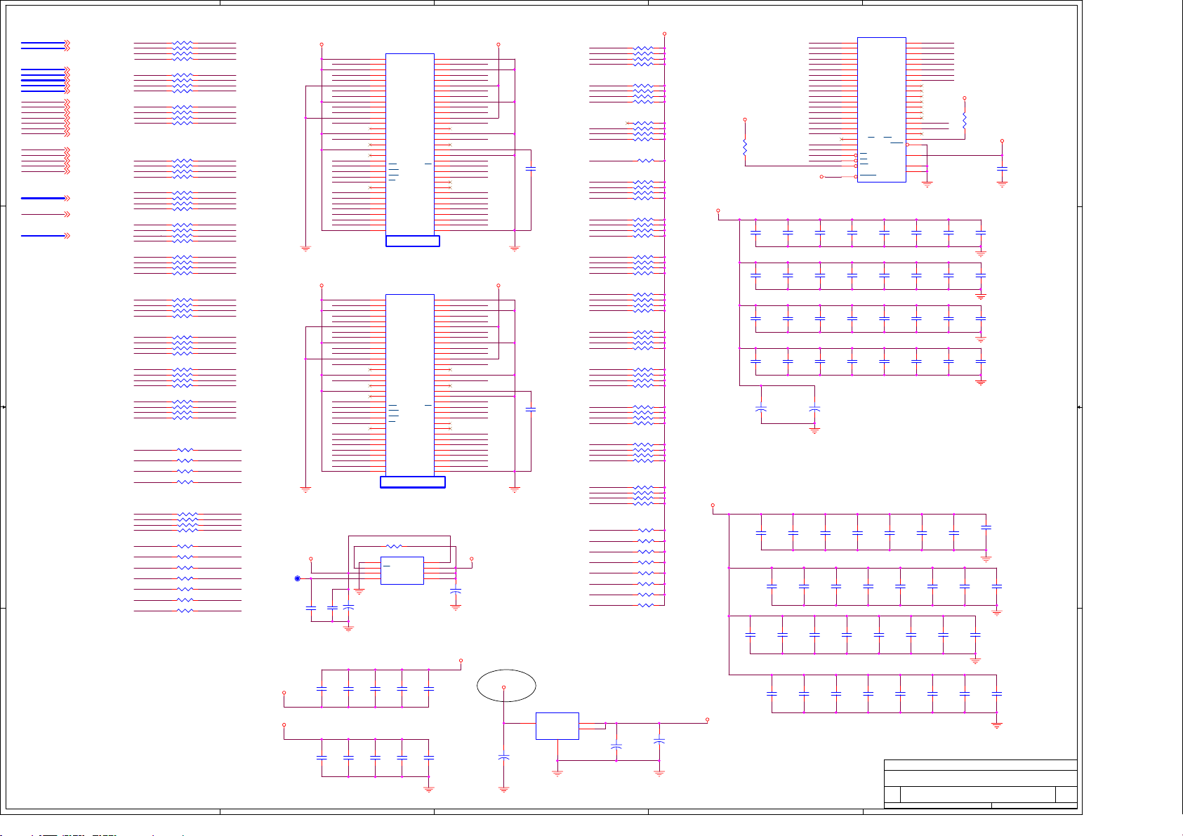
A_DQS[0..3]
A_RA[0..11]
A_BA[0..1]
A_DQM[0..1]
A_DQ[0..31]
A_CLK
A_CLK#
A_CKE
A_CS#
A_RAS#
A_CAS#
A_WE#
SDV25
VREF
IOWR#
IOCE#
F_A[0..21]
F_D[0..7]
F_OE#
ORO6
ORO7
ORO5
ORO4
ORO3
ORO2
ORO1
ORO0
MPX1
MPX2
VSYNC
HSYNC
VGASDA
VGASCL
RED+
REDGREEN+
GREENBLUE+
BLUE-
VGASOG
HSYNC_VGA
VGAVSYNC#
CVBS0+
CVBS0SY+
SYSC+
SCY+
YCB+
CBCR+
CR-
AP[0..7]
AN[0..7]
CLK1+
CLK1CLK2+
CLK2-
SCL
SDA
DACBCLK
DACMCLK
DACLRC
DOUT
SOY
CVBS1+
CVBS1-
R
G
B
PWM0
PWM1
AOSDATA1
OGO[0..1]
OBO[0..7]
TXD
RXD
MUTE
E
URST#
A_DQS[0..3] 5
A_RA[0..11] 5
A_BA[0..1] 5
A_DQM[0..1] 5
A_DQ[0..31] 5
A_CLK 5
A_CLK# 5
A_CKE 5
A_CS# 5
A_RAS# 5
A_CAS# 5
A_WE# 5
SDV25 5
VREF 5
IOWR# 5
IOCE# 5
F_A[0..21] 5
F_D[0..7] 5
F_OE# 5
ORO6 7
ORO7 1
ORO5 7
ORO4 7
ORO3 9
ORO2 7
ORO1 9
ORO0 10
MPX1 8
MPX2 8
OGO[0..1] 7
OBO[0..7] 10
VSYNC 9
HSYNC 9
VGASDA 6
VGASCL 6
RED+ 8
RED- 8
GREEN+ 8
GREEN- 8
BLUE+ 8
BLUE- 8
VGASOG 8
HSYNC_VGA 6
VGAVSYNC# 6
CVBS0+ 8
CVBS0- 8
SY+ 8
SY- 8
SC+ 8
SC- 8
Y+ 8
Y- 8
CB+ 8
CB- 8
CR+ 8
CR- 8
AP[0..7] 9
AN[0..7] 9
CLK1+ 9
CLK1- 9
CLK2+ 9
CLK2- 9
SCL 10
SDA 10
DACBCLK 10
DACMCLK 10
DACLRC 10
DOUT 10
SOY 7
CVBS1+ 8
CVBS1- 8
R9
G9
B9
PWM0 9
PWM1 10
AOSDATA1 10
TXD 6
RXD 6
MUTE 10
MiCO Confidential
610Thursday, September 15, 2005
V0.1
Page 22
A
21/100
B
C
D
E
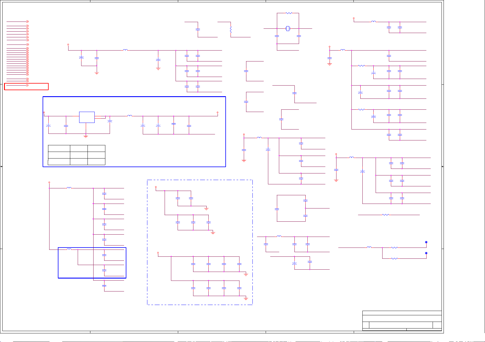
Power ON alive source
4 4
VCC
+
CE27
220uF/16v
3 3
C171
0.1uF
U9
1
ADJ/GND
SOT223
OUTIN
OUT
CM1117-3.3V
23
4
FB21
75R
0805
Vout
+
CE28
220uF/16v
DV33
C172
0.1uF
DV33
+5V
FB22
75R
0805
CE26
220uF/16v
+
C170
0.1uF
U10
M1117-3.3V
OUTIN
OUT
ADJ/GND
1
SOT223
23
4
+
CE29
220uF/16v
C173
0.1uF
DV33A
DV33A
C175
0.1uF
Vout
DV18A
U11
1
ADJ/GND
SOT223
OUTIN
OUT
CM1117-1.8V
23
4
CE31
+
220uF/16v
1.25x(1+300/680)=1.8V
U12
1
ADJ/GND
SOT223
OUTIN
OUT
CM1117-3.3V
23
4
+
CE32
220uF/16v
C176
10uF/10v
FB24
75R
0805
AV33
C177
0.1uF
AV33
FB23
75R
0805
+
CE30
100uF/16v
C174
0.1uF
1.25x(1+180/110)=3.3V
2 2
1 1
Title
MiCO LCD TV - MediaTek MT8203 Solution
Size Doc Number Rev
C
A
B
C
D
Date: Sheet of
LDO
E
MiCO Confidential
710Thursday, September 15, 2005
V0.1
Page 23
A
22/100
B
C
D
E
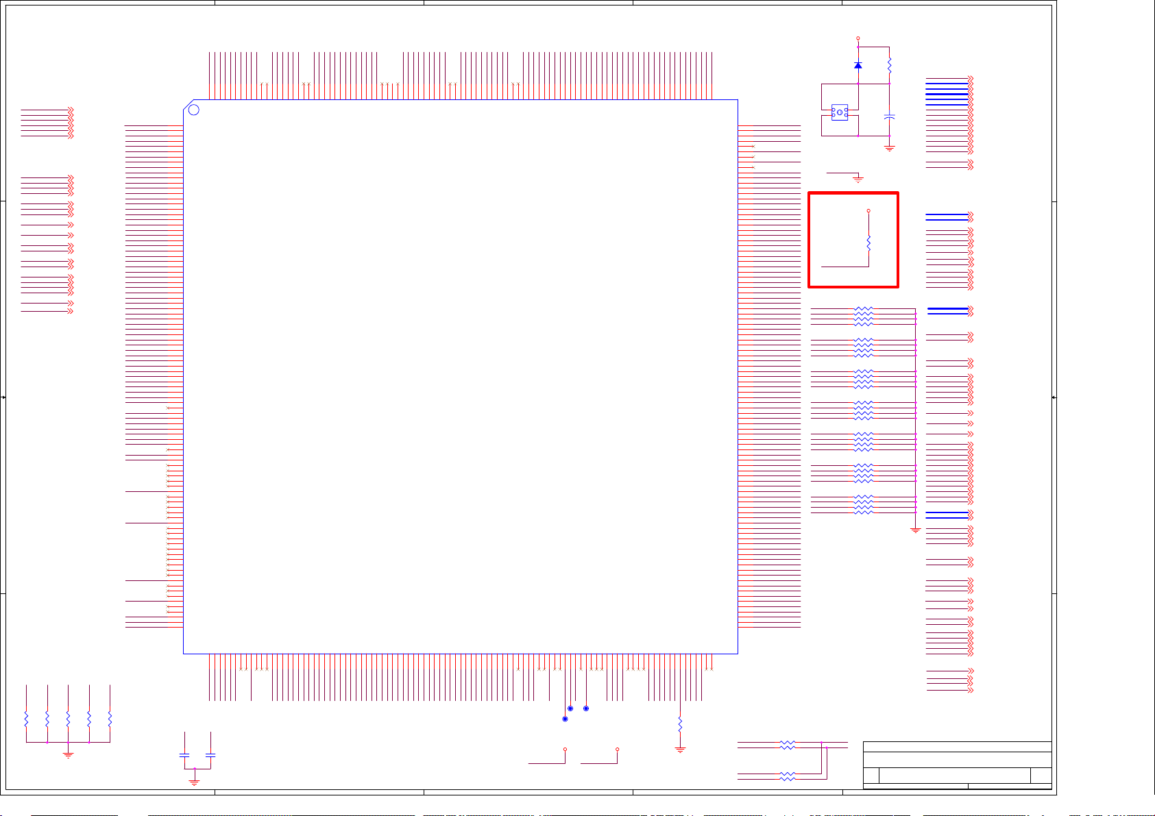
MT8203E (PBGA388) LCDTV BOARD 4 LAYERS
TXD
TXD 3,6
RXD
RXD 3,6
SCL_5V
SCL_5V 7,10
SDA_5V
01.INDEX & POWER CONNECTOR
4 4
02. LDO
03.MT8203 PBGA 388
04.MT8203 ANALOG&DIGIT DECOUPLE
1
2
3
4
5
6
7
8
+12V
+
+5V
C179
0.1uF
VCC
CE34
220uF/16v
C220UF16V/D6H11
SYSTEM EEPROM
1
2
3
4 5
EEPROM 24C16
SOP8
+12V
U13
NC
NC
NC
GND SDA
J4
5
4
3
2
1
5x1 W/HOUSING
SIP5\2
FB26
75R
0805
8
VCC
7
WP
6
SCL
SYS_PWR
For Tuner
05.DDR MEMORY & FLASH
J3
06.VGA IN & PC AUDIO IN
07.VIDEO IN & TUNER IO
08. AV IN
09.LVDS/CRT/BACK LIGHT CONTROL
10.AUDIO WM8776/ KEYPAD
3 3
HOLE/GND
H1
9
9
8
8
7
7
6
6
9
9
8
8
7
7
6
6
2 2
9
9
8
8
7
7
6
6
9
9
8
8
7
7
6
6
2
2
3
3
4
4
5
5
1
1
HOLE/GND
H2
1
1
HOLE/GND
H3
1
1
HOLE/GND
H4
1
1
FB25
120R
2
2
3
3
4
4
5
5
FB27
120R
2
2
3
3
4
4
5
5
FB30
120R
2
2
3
3
4
4
5
5
FB31
120R
DIP8/P2.0
TO Power BD
+
+5V
+
CE35
47uF/16v
SCL_5V
SDA_5V
+5V
+5V
2 3
CE33
220uF/16v
C220UF16V/D6H11
+5V
R100
4.7k
R98
10k
Q3
1
SOT23
2N3904
TUNER_12V
C178
0.1uF
R101
4.7k
ORO7 High :POWER OFF
ORO7 LOW :POWER ON
R99
ORO7
4.7k
FOR Tuner
DIGITAL GNDAUIO IN/OUT GND ANALOG INPUT GND
+12V
TUNER_12V
ORO7
SDA_5V 7,10
+12V 9
TUNER_12V 7
ORO7 3
1 1
Title
MiCO LCD TV - MediaTek MT8203 Solution
Size Doc Number Rev
C
A
B
C
D
Date: Sheet of
INDEX & POWER CONNECTOR
E
MiCO Confidential
810Thursday, September 15, 2005
V0.1
Page 24
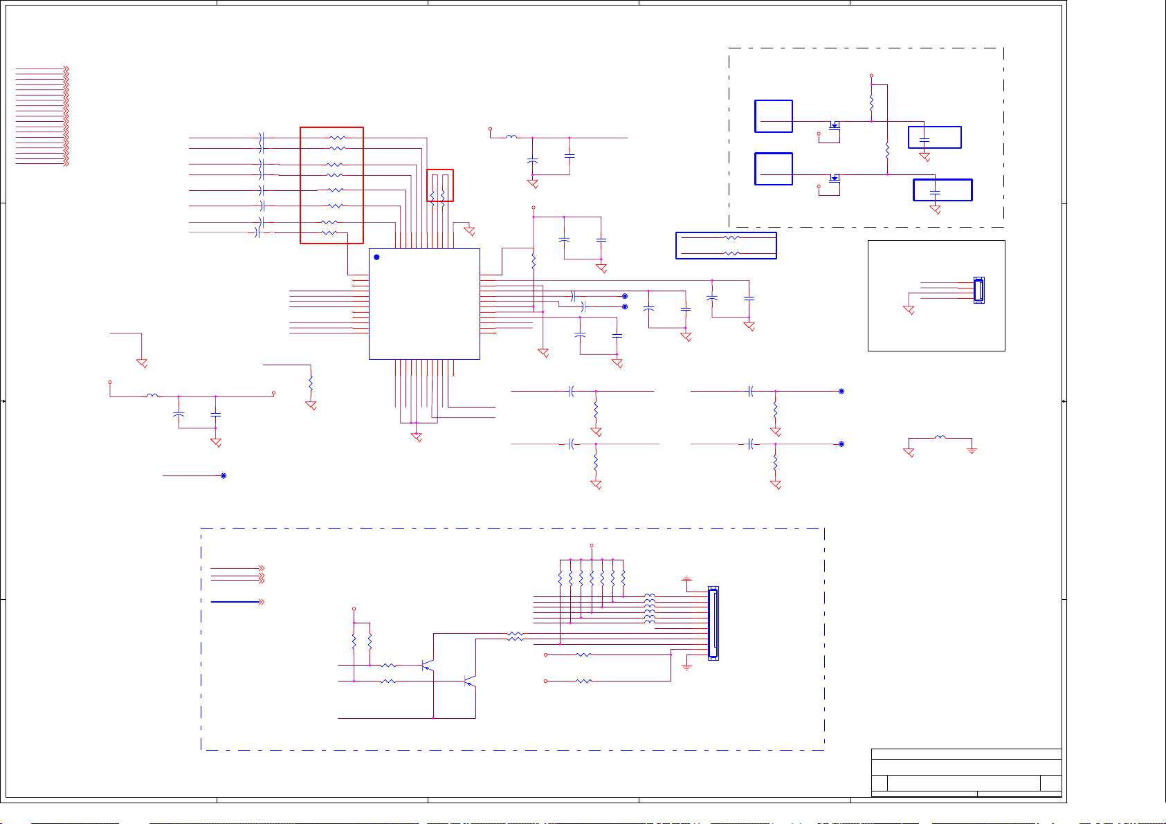
A
23/100
B
C
D
E
S1_AV1_L
S1_AV1_R
VGA_IN_L
VGA_IN_R
YPBPR1_L
YPBPR1_R
YPBPR2_L
YPBPR2_R
4 4
SCL
SDA
DACBCLK
DACMCLK
DACLRC
DOUT
AOSDATA1
PWM1
MUTE
SCL_5V
SDA_5V
3 3
S1_AV1_L 7
S1_AV1_R 7
VGA_IN_L 6
VGA_IN_R 6
YPBPR1_L 7
YPBPR1_R 7
YPBPR2_L 7
YPBPR2_R 7
SCL 3
SDA 3
DACBCLK 3
DACMCLK 3
DACLRC 3
DOUT 3
AOSDATA1 3
PWM1 3
MUTE 3
SCL_5V 1,7
SDA_5V 1,7
DV33
YPBPR2_R
YPBPR2_L
VGA_IN_R
VGA_IN_L
S1_AV1_R
S1_AV1_L
YPBPR1_R
YPBPR1_L
GND
FB33
DV33
0603 120R
+
CE53
47uF/16v
PWM1
Del Parts
CE36 10uF/25v
CE37 10uF/25v
CE39
CE40
CE41 10uF/25v
CE42 10uF/25v
CE43 10uF/25v
CE44 10uF/25v
DVDD
C187
0.1uF
TP10
+
MODIFIED FROM 10K-->100K BY BIN_WANG .16/7/05.AVOID AUDIO BOMB WHEN OPEN THE POWER
+
+
+
+
+
+
+
DVDD
10uF/25v
10uF/25v
DACLRC
R102 100k
R104 100k
R106
R107
R108 100k
R111 100k
R112 100k
R113 100k
DACMCLK
AOSDATA1
DACLRC
DACBCLK
DACMCLK
DOUT
R114
1k
100k
100k
U14
1
AIN2L
2
AIN1R
3
AIN1L
4
DACBCLK
5
DACMCLK
6
DIN
7
DACLRC
8
ZFLAGR
9
ZFLAGL
10
ADCBCLK
11
ADCMCLK
12
DOUT
TWO WIRE SERIAL CONTROL DEVICE ADDRESS 0x34h
MODIFIED FROM 10K-->100K BY BIN_WANG .16/7/05.AVOID AUDIO BOMB WHEN OPEN THE POWER
R110 50k
R109 50k
48
AIN5L
AIN4L
AIN3L
AIN5R
AIN4R
AIN3R
AIN2R
ADCLRC
1314151617181920212223
DACLRC
DGND
DVDD
DVDD
MODECEDICLHPOUTL
SDA14
SCL14
AINVGL
AINOPL
HPGND
AINOPR
HPVDD
HPVDD
3738394041424344454647
AGND
AINVGR
AVDD
ADCREFP
ADCREFGND
VMIDADC
AUXL
AUXR
DACREFP
DACREFN
VMIDDAC
VOUTR
VOUTL
HPOUTR
NC
WM8776
24
CODHPOUTR
CODHPOUTL
NC
36
35
34
33
32
31
30
29
28
27
26
25
VCC
FB32
0603 120R
HPVDD
VMIDADC
AUXL
AUXR
HPVDD_A
COD_VOUTR
COD_VOUTL
COD_VOUTR
COD_VOUTL
HPVDD
CE38
+
10uF/25v
+
R193
33R
ADCREFP
CE46 10uF/25v
CE48 10uF/25v
VMIDDAC
CE51
+
10uF/25V
CE54
+
10uF/25v
C180
0.1uF
CE45
10uF/25v
+
+
HPVDD
+
CE50
10uF/25v
R115
R117
ADCREFP
CE49
10uF/25v
SCL
SDA
C185
0.1uF
CODHPOUTL HPOUTL
C183
0.1uF
VMIDADCDACBCLK
TP6
+
TP7
C186
0.1uF
AUSPR
10k
AUSPL
10k
Modify I2C by Zheng.Guo. 16/8
R207 33
R/SMD/0603
R208 33
R/SMD/0603
+
CE47
10uF/25v
CE52
+
220uF/16v
CE55
+
220uF/16v
SCL14
SDA14
C184
0.1uF
SCL_5V
SDA_5V
R116
R118
DV33A
R190
4.7k
SCL
C181
10pF
R192
4.7k
SDA
C182
10pF
J5
1
2
3
4
4x1 W/HOUSING
SIP4\2
MUST USE SHIELD CABLE
MUTE
AUSPR
AUSPL
DV33A
DV33A
QF1
2N7002
312
QF2
2N7002
312
TO AUDIO BD
TP8
HPOUTRCODHPOUTR
47k
TP9
47k
FB28
0603 120R
2 2
ORO0
URST#
IR
OBO[0..7]
1 1
A
ORO0 3
URST# 3
IR 3,7
OBO[0..7] 3
ORO0 High :SYSTEM POWER OFF
ORO0 LOW :SYSTEM POWER ON
DV33A
R120
R121
10K
10K
DV33A
OBO6
OBO7
R0603
R124 4.7K
R125 4.7K
R0603
B
OBO0
OBO1
OBO2
OBO3
OBO4
OBO5
R119 510
LED_RED
R122 510
LED_GRN
ORO0
Q4
1
2N3906
2 3
Q5
1
2N3906
2 3
DV33A
+5V
C
KEYPAD - MAX 8-KEYS
+5V
R197
R196
R195
R194
10k
10k
R123 NC/0
R126 0
10k
10k
POWER ON/OFF
R199
R198
10k
10k
IR & POWER ON LED
R200
10k
FB34 FB
FB35 FB
FB36 FB
FB37 FB
FB38 FB
FB39 FB
TV/AV
MENU
VOLVOL+
CHCH+
IR
J6
1
2
3
4
5
6
7
8
9
10
11
12
13
13x1 W/HOUSING
SIP13\2
Title
MiCO LCD TV - MediaTek MT8203 Solution
Size Doc Number Rev
C
D
Date: Sheet of
AUDIO WM8776/ KEYPAD
E
MiCO Confidential
910Wednesday, September 28, 2005
V0.1
Page 25
A
24/100
TU_VCC
AV , TUNER I/O
4 4
Y
Y_GND
CB
CB_GND
CR
CR_GND
SOY
SY
SY_GND
SC
SC_GND
CVBS0
TV_GND
CVBS1
CVBS1_GND
SIF1_OUT
AF1_OUT
SCL_5V
SDA_5V
TUNER_12V
OGO[0..1]
ORO6
ORO4
ORO5
ORO2
S1_AV1_L
S1_AV1_R
3 3
YPBPR1_L
YPBPR1_R
YPBPR2_L
YPBPR2_R
+12V
2 2
ORO6
Y8
Y_GND 8
CB 8
CB_GND 8
CR 8
CR_GND 8
SOY 3
SY 8
SY_GND 8
SC 8
SC_GND 8
CVBS0 8
CVBS0_GND 8
CVBS1 8
CVBS1_GND 8
SIF1_OUT 8
AF1_OUT 8
SCL_5V 1,10
SDA_5V 1,10
TUNER_12V 1
OGO[0..1] 3
ORO6 3
ORO4 3
ORO5 3
ORO2 3
S1_AV1_L 10
S1_AV1_R 10
YPBPR1_L 10
YPBPR1_R 10
YPBPR2_L 10
YPBPR2_R 10
+12V 1,9
IR 3,10
OGO0
OGO1
ORO5
VCC
TUNER_12V
ORO4IR
R157
4.7k
R162
4.7k
VCC
TU_12V
SDA_5V
SCL_5V
SIF1_OUT
AF1_OUT
TV_GND
CVBS0
FB41
70R
CE56
+
1000uF/16v
FB43
70R
+
DVD Connector
VCC
8/18 modify by steven
R149
10k
IR
VCC
10k
R156
SOT23
2N3904
1
Q8
2 3
CE57
1000uF/16v
1
VCC
CVBS0---TUNER1
CVBS1---FRONT BD AV_IN
J7
1
2
3
4
5
6
7
8
9
10
11
12
CON12
SIP12\2
TU_VCC
C188
0.1uF
TU_12V
C189
0.1uF
VCC
R146
10k
IR_DVD
SOT23
2N3904
Q6
2 3
Q7
1
S1
D1
2
G1
D1
3
S2
D2
4 5
G2 D2
IR7314
SOP8
470uF/16v
C470UF16V/D8H14
NEARLY YPBPR1-CON.
ORO6
OGO0
0
HP_SENSE
OGO1
TP11
A
R169
1 1
Y1_GNDB
CB1_GNDB
CR1_GNDB
NEARLY YPBPR2-CON.
Y2_GNDB
CB2_GNDB
CR2_GNDB
R179
15K
YPBPR1/L
YPBPR1/R
YPBPR2/L
YPBPR2/R
MODIFIED FROM 15k-->0 BY BIN_WANG 16/7/05.
YPBPR1_L
R180
15K
15K
15K
R187
R188
YPBPR1_R
YPBPR2_L
YPBPR2_R
B
DIP11X2/P2.54/R2
VIDEO CONNECTOR
VCC
Y1_INB
Y1_GNDB CB1_GNDB
CR1_INB
CR1_GNDB
CVBS1
CVBS1_GND
SC
SC_GND
SY SY_GND
J9
YPBPR2/R
1
YPBPR2/L
2
3
IR_DVD
4
CB2_GNDB
5
CB2_INDVD
6
Y2_GNDB
7
Y2_INDVD
8
CR2_GNDB
9
CR2_INDVD
10
CON10
C190
0.1uF
J10
1
2
3
4
5
CON5
VDVD
8
7
6
CE63
+
2122
20
18
16
14
12
10
8
6
4
2
J9
CB1_INB
19
17
15
YPBPR1/L
13
YPBPR1/R
11
9
AV_L
7
AV_R
5
3
1
Y2_INDVD
Y2_GNDB
CB2_INDVD
CB2_GNDB CB2_GNDB
CR2_INDVD
1
3
1
3
1
C
VCC
R158 0
3
D7
BAV99
2
VCC
R165 0
D8
BAV99
2
VCC
R168 0
D9
BAV99
2
VCC
R160
75
R167
75
R170
75
Y2_GNDB
CR2_GNDBCR2_GNDB
Y2B
CR2B
Added by Zheng_guo 21/7/05
Y1_INB
CE58 22uF/10V
+
Y1_GNDB
CB1_GNDB
CB2B
CR1_INB
CR1_GNDB
CE61 22uF/10V
Y2_GNDB
CB2B
CB2_GNDB
CR2B CR2SWB
CR2_GNDB
R139
CE59 22uF/10V
+
CE60 22uF/10V
+
+
CE62 22uF/10V
+
CE64 22uF/10V
+
10K
R143
10K
R148
10K
R154
10K
R161
10K
R166
10K
D
VCC
R137
10K
VCC
R140
10K
VCC
R144
10K
VCC
R151
10K
VCC
R155
10K
VCC
R163
10K
Optional for one component.Added by Bin_wang 14/7/05
Y1SWB
CB1SWBCB1_INB
CR1SWB
Y2SWB
CB2SWB
R138
0/NC
R141
0/NC
R147
0/NC
R153
0/NC
R159
0/NC
R164
0/NC
CB
CR
CB
CR
Y
YY2B
E
COMPONENTS SWITCH.
DV33
R171
10K
ORO2
CB1SWB
CB2SWB
CB
Y1SWB
Y2SWB
Y
GNDS
AV_L S1_AV1_L
R176 15K
AV_R S1_AV1_R
R177 15K
YPBPR2_R
YPBPR2_L
S1_AV1_R
S1_AV1_L
YPBPR1_R
YPBPR1_L
R181
R182
75K
75K
B
R183
75K
R184
75K
R185
75K
R186
75K
C
MODIFIED BY BIN_WANG.16/7/05
CR_GND
CB_GND
Y_GND
D
U15
1
2
3
4
5
6
7
8
R178
Y
0
S
VCC
I0A
I1A
YA
I0B
I1B
YB
GND
IDTQS3VH257
TSSOP16/SMD
16
GNDS
15
E#
14
I0D
13
I1D
12
YD
CR1SWB
11
I0C
CR2SWB
10
I1C
CR
9
YC
C191
SOY
4.7nF
DV33
FB46
70R
Title
MiCO LCD TV - MediaTek MT8203 Solution
Size Doc Number Rev
C
Date: Sheet of
VIDEO IN & TUNER IO
E
MiCO Confidential
10 10Thursday, September 15, 2005
V0.1
Page 26
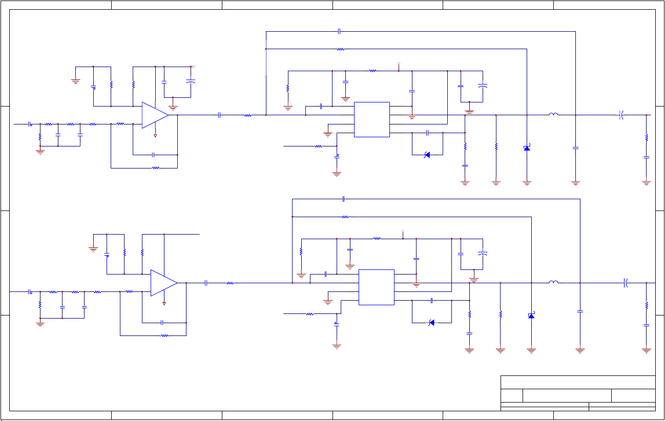
54321
C1
12
22pF NPO
12
5%
1 2
R7
5%
10K
5%
NPO
4.7nF
C8
NPO
4.7nF
C30
1 2
12
12
82K
R1
C15
2.2UF
C21
22pF NPO
5%
R14
82K
C34
NS
12
1
2
3
4
A
C5
4.7uF
X5R
PIN
NIN
AGND
EN
12
12
12
C27
4.7uF
X5R
1
2
3
1 2
U1
ATA-120
R2
5%
100K
PGND
SW
VPP
BS
R16
1 2
5%
100K
U3
PIN
PGND
NIN
AGND
EN4BS
ATA-120
+24V
12
12
+
C4
C6
100NF
1 2
X7R
8
7
6
C9
1 2
5
1UF
X5R
D2
6.2V
C7
100UF/25V
1UF
X7R
L5 10uH
1 2
12
12
R8
10
5%
5%
12
C17
390PF
NPO
D1
R9
MBRS130LTR
10K
12
+24V
12
12
+
C25
C28
100NF
1 2
X7R
8
7
SW
6
VPP
C32
1 2
5
1UF
X5R
D4
6.2V
C29
100UF/25V
1UF
X7R
L6 10uH
1 2
12
12
5%
12
C36
390PF
NPO
R23
R22
10
10K
5%
D3
MBRS130LTR
D
+24V
12
12
R11
R10
10K
10K
5%
C14
22UF/16V
AUSPL
C20
10UF
5%
R66
R47
12
4K7
1K8
5%
5%
C541nC55
R4
100K
1 2
C
B
AUSPR
C40
10UF
R45
R33
12
4K7
1K8
5%
5%
R19
C521nC53
100K
5%
1 2
5%
R67
1 2
12
12
4K7
5%
1n
C19
22UF/16V
R46
12
12
4K7
5%
1n
3
R12
2
10K 5%
12
R37
10K
5%
R39
1 2
10K 5%
U2A
+
-
AGND
C24
22pF
R15 47K
1 2
12
R36
10K
5%
U2B
5
+
6
-
OUT
AGND
1 2
12
+
C10
C12
100UF/25V
100NF
C3
1
RC4558
5%
1 2
+24V
R3
12
5%
1UF
10K
X5R
MUTEC
R5
5%
100K
1 2
R17
100K
1 2
R18
C31
5%
1 2
7
OUT
RC4558
C41
22pF
47K
R38
5%
1UF
X5R
12
10K
R21
MUTEC
5%
10K
6
D
FILM
C38
1 2
+
1000UF/25V
12
R6
10
C11
470NF
5%
C16
C
100NF
1 2
X7R
B
C39
1 2
+
1000UF/25V
12
C33
470NF
FILM
12
R20
10
5%
C35
100NF
1 2
X7R
A
A
Title
Number RevisionSize
B
1 2 3 4 56
25/100
Date: 2-Sep-2005 Sheet of
File: D:\
正在进行的项目\LCD TV\LCD TV.Dd bDrawn By:
Page 27
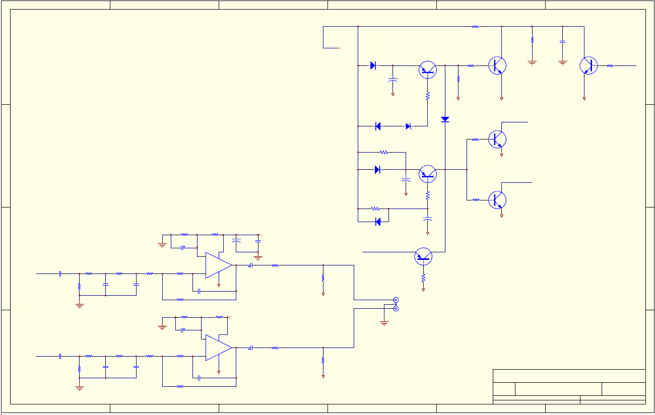
54321
R24
3K
12
5%
D
+24V
D6
1N4148
AGND
D8
1N4148
R43
C
0R
D5
NC
R30
22k
D9
R54 10K
1 2
C22
5%
5%
22U/16V
R51 10K
1 2
R52 22K
1 2
R62 10K
1 2
R59 10K
1 2
R64 22K
1 2
B
AUSPL
R48 1k8
C60
1 2
12
10UF
X5R
R49 4K7
1 2
12
5%
5%
R53
1n
100K
R50 4K7
1 2
12
5%
C45
C46
1n
1 2
C59
A
AUSPR
12
10UF
X5R
1 2
5%
R60
100K
5%
1 2
12
1n
R57 4K7
R56 1k8
R58 4K7
1 2
12
5%
C47
C48
1n
1 2
1 2 3 4 56
5%
5%
1 2
5%
5%
C44
22U/16V
5%
1 2
5%
R55 10K
1 2
U5A
3
+
2
-
RC4558
C49
22P
1 2
U5B
5
+
6
-
RC4558
C50
22P
5%
AGND
R63 10K
AGND
12
+24V
C2
C13
100U/35V
100N
C26
R13
1
OUT
10U/16V
12
5%
1K
R65
47K
5%
1 2
AGND
1N4148
MUTE
LOUT
ROUT
+24V
5%
C43
R26
7
OUT
10U/16V
12
5%
1K
R61
47K
5%
1 2
AGND
26/100
Q1
2N3906
12
+
C42
100UF/25V
4.7V
AGND
J10
R42
1k
D7
Q4
2N3906
12
+
C18
NC
R28
1k
12
+
C51
220UF/25V
AGND
Q7
NC
R27
NC
AGND
R40
10K
12
12
5%
R41
5%
10K
AGND AGND
D10
NC
R34
12
5%
1K
MUTEB
R35
1 2
5%
1K
AGND
AGND
rca2
Title
B
Date: 2-Sep-2005 Sheet of
File: D:\
12
R25
5%
10K
1 2
Q2
2N3904
LOUT
Q5
2N3904
ROUT
Q6
2N3904
Number RevisionSize
正在进行的项目\LCD TV\LCD TV.Dd bDrawn By:
6
MUTEC
C37
1UF
X5R
Q3
2N3904
R29
1K
5%
D
12
MUTE
AGND
C
B
A
Page 28
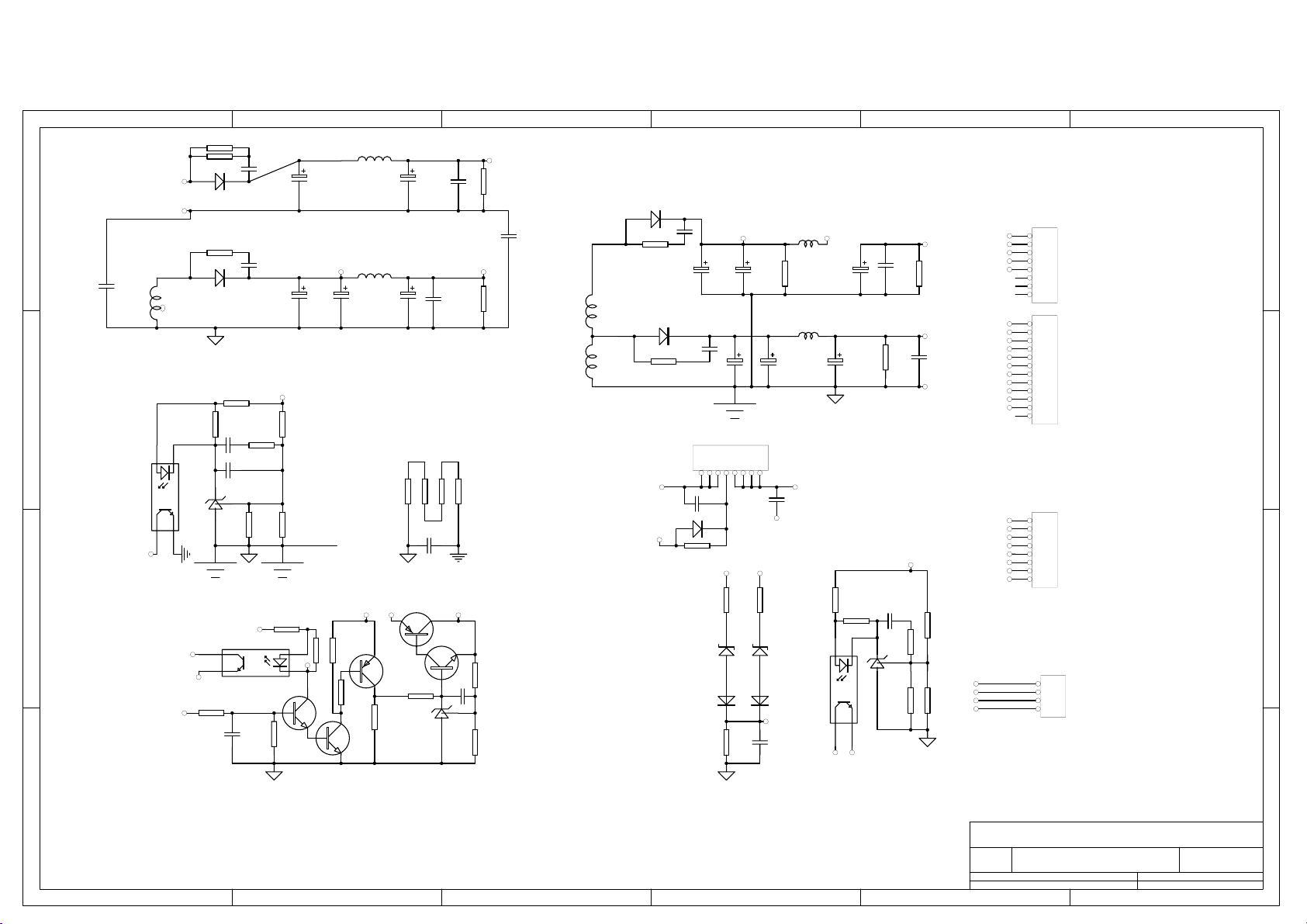
54321
C7
NC
EC22
470U/35V 105 KM 10*16
C6
NC
EC14
470U/35V 105 KM 10*16
R100
R101
4.7M
4.7M
CY3
102/400V Y1
Q205
TIP32
12V
Q209
4401
R116
470R
TL431
C47
104
IC30
24V
R102
4.7M
R117
13K1%
R118
3.3K1%
A24V
R132
2K/2W
R103
2K/2W
C54
NC
T2C
T2D
9 7
8 9
D19
C38
Y2010D
102/1KV
100R
R104
EC11
1000U/25V KM10*20
Y2045
D20
C39
100R
R106
5.7V
C50
224/25V
D30 LBD914
28A
R130
68K
D17B
LBAV70
1000U/25V KM10*20
8A
EC18
102/1KV
1000U/16V KF10*16
FG2
IC7
8 HEADER
1234567
R94
200R
Z6
6.2V
R62
1K
EC12
EC19
1000U/16V KF10*16
8
C51
224/25V
SGND
24V5.7V
R26
300R
Z8
27V
D17A
LBAV70
30A
C42
224/25V
L7
3UH 4*20
36A
R84
3.3K
L5
1.5UH 4*20
1000U/16V KF10*16
+5V
R27
470R
IC5
TL431A
P3
PC817B
EC15
470U/16V KM8*11
EC20
R86
3.3K
16A 17A
NC
R110
1K/1W
C44
224/25V
R87
3.3K
R119
3.3K1%
C8
5.0V
12V
R111
1K/1W
5.0V
C40
224/25V
SGND
R120
150K1%
3.3K1%
R52
A24V
A24V
1
STB
12V
12V
12V
+5V
+5V
+5V
+5V
+5V
24V
24V
24V
24V
2
CON2
3
4
PH5
5
6
7
8
1
2
CON1
3
4
PH11PIN
5
6
7
8
9
10
11
12
1
2
3
CON3
4
5
6
XH8PIN
7
8
1
CON4
2
3
PH4PIN
4
SGND
SGND
5.0V
5.0V
SGND
SGND
SGND
SGND
SGND
SGND
SGND
B2
B2
A2
B2
R60
1K
P1
PC817B
IC6
TL431A
200R
200R
HER303
D21
470U/35V 105 KF10*20
L4
3.5*1.5*5
D18
FCH20A150
1000U/35V 105 KF13*20
R96
2.2K
C30
104/25V
C23
103/50V
C52
471/1KV
EC21
C37
471/1KV
EC9
R89
68K
1000U/35V 105 KF13*20
24V
R98
27K+-1%
R61
1K
R112
3.3K1%
R131B
R131A
D
T3E
MLT066-T2
C53
471/1KV
10 9
C
18A
EC10
6A
L11
3.3UH 3*20
L6
1.5UH 4*20
R99
4.7M
FG3 FG4
R25
B
PC817B
18V
SWB
R85
STB
3.3K
PS-ON
C41
224/25V
P4
5.7V
R20
10K
R24
300R
300R
R113
36A
8A
1K/1W
3
28A
Q20
4401
1
B
E
R114
3.3K
Q200
4401
Q202
B
4403
C
2
R115
10K
1
2
C
E
3
6
D
C
B
A
Title
Number RevisionSize
B
1 2 3 4 56
27/100
Date: 23-Jan-2006 Sheet of
File: F:\ \MLT166A.DDB
MLT166A-SCH3
软环境 Drawn By:
A
Page 29
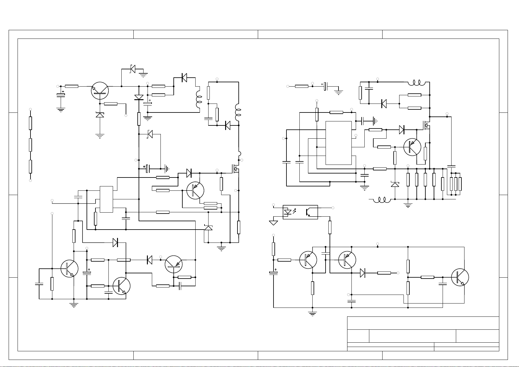
321
4
D
C
B
A
启动
13A
11A
C25
104/25V
R53
240K
R54
240K
R55
240K
VCC
EC3
100U/35V
16A
17A
R74
20K
R29
10R
C13
331/50V
R76
33K
Q9
4401
26A
R77
Q12
4401
Z2
15V
33K
EC7
4.7UF/50V
R75
R56
IC2
1
2
3 4
LD7550A IL
R79
82K1%
D15
20K
C26
104/25V
1K
6
5
331/50V
3.3K
Z3
27V/1W
D7
LBD914
SWB
R63
100R
C14
LBD914
R80
T2A
D12
D8
R19
C27
104/25V
MLT066-T3
1
1
2
2
C17
222/1KV B
LBD914
470R
Q3
4403
R71
13A
Q10
5N80
35A
R31
Z5
9.1V/1W
R11
47R
R67
68K/2W
D13
HER207
R125
10K
9A
10R
10K
R81
0.62R/2W
T2B
4 3
L10
3.5*1.5*5
10A
103/50V
OVP
EC8
22UF/50V
30A
18A
VCC
18A
C22
1
2
R49
20K
P2
A
K
PC817B
R50
20K
R123
47R
C34
222/16V NPO
33K
32A
VREF
C
E
Q6
R78
EC6
10U/50V
R48
20K
4403
R69
12K 1%
IC3
1
2
3
4 5
3843
4
3
R17
5.1K
C28
104/25V
C35
224/25V
HER103
R65B
18V
10R
R65A
Z7
27V
10R
EC4
100U/35V
EC5
22UF/50V
11A
R73
47R
R23
470R
R57
1K
D10
LBD914 Q15
Q13
4401
4A
R82
3.3K
Q5
4403
18V
C15
331/50V
4A
R68
68K/2W
VREF
8
7
6
Title
32A
C24
104/25V
4403
25A
D9
LBD914
13A
C18
HER207
R72
47R
R22
470R
R70
470R
Z4
9.1V/1W
T3B
MLT066-T2
VREF
R58
1K
222/1KV B
D3
LBD914
R18
10K
R88
D14
43
68K
R12
R13
R45
25A
T3A
MLT066-T2
7NK80
1A
R46
2.2R
RTC1
2K
2.2R
47R
47R
R41
R124
3.3K
Q4
4403
1R
C29
104/25V
R30
10R
R90
2.2R
R42
D
31A
Q11
C33
101/1KV
R93
R92
R91
1R
200R
200R
4401
200R
Q14
C
B
A
Number RevisionSize
A4
Date: 23-Jan-2006 Sheet of
1 2 34
File: F:\ \MLT166A.DDB
MLT166A-SCH2
软环境 Drawn By:
28/100
Page 30
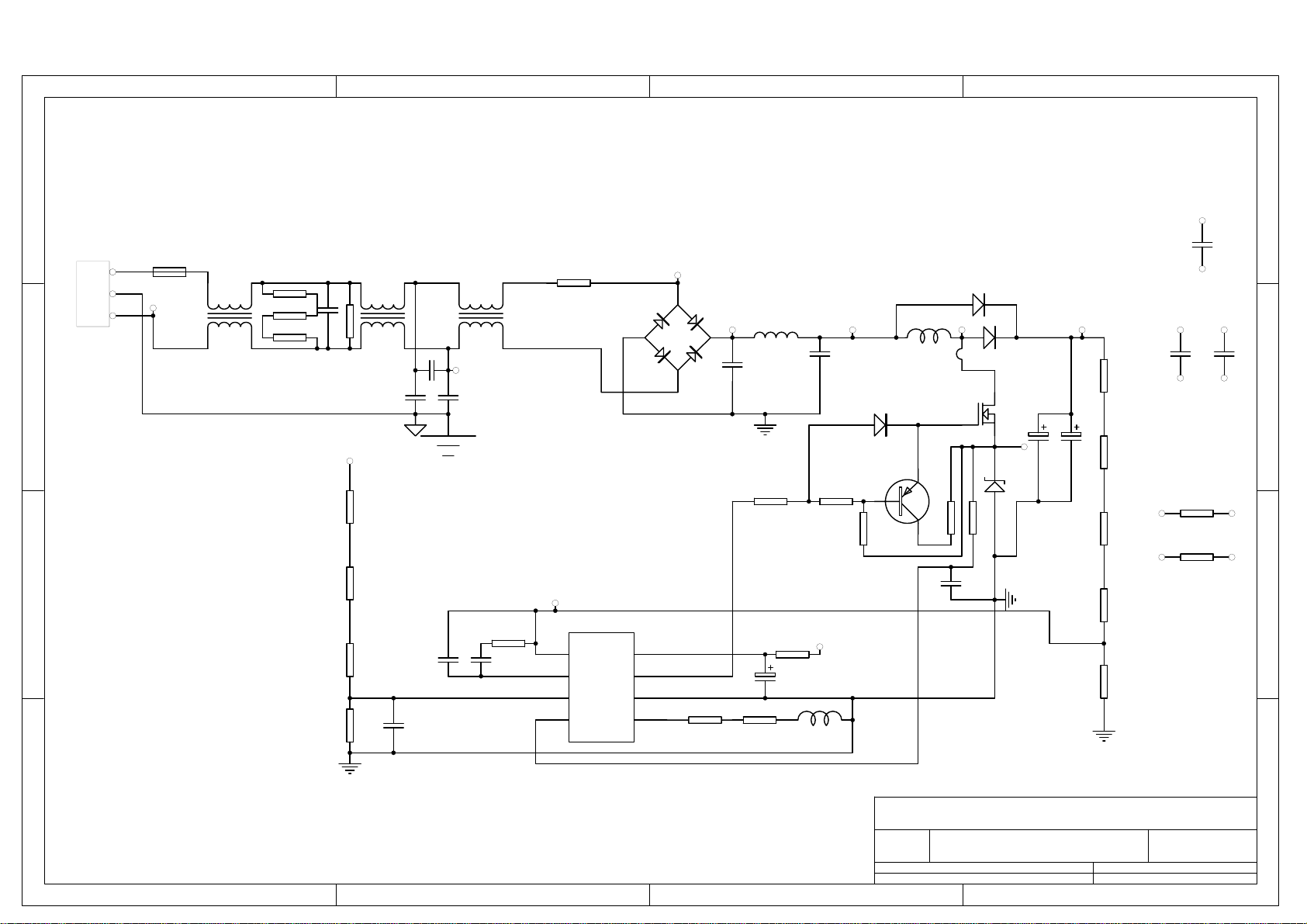
321
4
D
82.8效率 % 1W2.7W
2A
102/500V
D
C2
CON0
1
2
3
VH3.69-5-3
C
F1
T5AH/250V 5*20
5A
MLT070A-L101
HL1
R4
R3
R2
510K
510K
510K
CX1
0.47U/275V
L1
R1
14D681
471/400V Y1
MLT066A-L1
CX2
0.1U/275V
CY2
L2
MLT066A-L1
7A
CY1
471/400V Y1
NTC1
5D-13
34A
1
BG1
D3SBA60
2A
4
2
C10
1U/450V
3
L3
MLT042-L3
C11
1U/450V
21A
PL1A
MLT066-T1
442
Q8
18N50
D4
1N5406
22A
L8
3.5*5
D5
FUS05B60
2
13A
R36
470K+-1%
C16
13A
19A
GND
223/630V
13A
GND
102/500V
C1
C
EC2B
R35
2A
FG1
R5
510K
R9
47R
R6
B
510K
C5
NC
R7
510K
R47
20K
C3
474/25V
C21
103/50V
IC1
R8
NC
20A
1
2
3
4 5
R122
10R
VCC
8
7
6
R15
10K
R16
10K
EC1
10U/50V
PL1B
665
R21
470R
R14
10K
D2
LBD914
5
C12
331/50V
Q2
4403
R28
10R
R32
300R
19A
Z1
9.1V/1W
22U/450V KM 13*25
R33
470K+-1%
R34
100K+-1%
R51
10K1%
EC2
470K+-1%
19A
19A
68U/450V KM 18*30
1R
R37
R43
0.39R/2W
GND
GND
B
L6562D
A
1 2 34
Title
Number RevisionSize
A4
Date: 23-Jan-2006 Sheet of
File: F:\ \MLT166A.DDB
软环境 Drawn By:
A
29/100
Page 31

Basic Operations & Circuit Description
30/100
Main Electric Components
(1). MODULE:
There are 1 pc. panel and 2 pcs. PCB including 1 pc. INVERTER
board(L), 1 pc. T-CONTROL board,
(2).SIGNAL PROCESS
There are 5 pcs. PCBs including
1 pc. Audio&Tuner board,
1 pc. Main digital board,
1 pc. Keypad board,
1 pc. Remote Control Receiver board,
1 pc. DVD decoder board
(3).POWER
There are 1 pc. PCB for power.
Page 32

PCB function
31/100
1. Power:
(1). Input voltage: AC 100V~240V, 47Hz~63Hz.
Input range: AC 90V(Min)~264V(Max) auto regulation.
(2). To provide power for PCBs.
a). +24V for Inverter.
b). +5Vsb for standby,
c). +5V for signal power,
d). +24V for Audio Amp power and converter to
e). +12V for Tuner power.
2. Main (Video InterFace) board:
(1).Decoder the video signal (TV,CVBS,S-VIDEO) from analog to digital
signal.
(2).Converter the Video signals( TV,CVBS,S-VIDEO ) and graphics signal
(VGA,YPbPr) from interface to progressive,
(3). Converter the Digital to fit the panel display mode and output the LVDS
signal to Panel.
3. Tuner & Audio Board:
(1)
(2 ). Decoder the TV SIF signal to audio signal,
(3 ). Converter the audio to audio Amplifier and output to the speaker.
4. KEYBOARD
To get the main button control on LCD_TV as SOURCE,MENU,
CHANEL +,CHANEL -, VOL +,VOL-, STANDBY functions.
5. Remote control board
Receive the remote signal and active for the control.
6. T-CONTROL board
7. INVERTER board
Convert TV RF signal to video and audio signal to Main board.
Converter the LVDS signal to the digital signal for fitting the PANEL.
Converter the low DC voltage +24V to high AC voltage to drive the backlight.
Page 33

PCB failure analysis
32/100
1. CONTROL:
a. Abnormal noise on screen.
b. No picture.
2. MAIN (VIDEO):
a. Lacking color, Bad color scale.
b. No voice.
c. No picture but with signals output, OSD and back light.
d. Abnormal noise on screen.
3. POWER:
No picture, no power output.
Basic operation of LCD-TV
1. After turning on power switch, power board sends 5Vst-by Volt to Micro
Processor IC waiting for ON signals from Key Switch or Remote Receiver.
2. When the ON signal from Key Switch or Remote Receiver is detected, Micro
Processor will send ON Control signals to Power. Then Power sends (5Vsc,
12Vsc, 24V and RLY ON, Vs ON) to PCBs working. This time VIF will send
signals to display back light, OSD on the panel and start to search available
signal sources. If the audio signals input, them will be amplified by Audio AMP
and transmitted to Speakers.
3. If some abnormal signals are detected (for example: over volts, over current,
over temperature and under volts), the system will be shut down by Power off.
Page 34

LCD basic display theory.
33/100
When an electrical field is applied to the LC planes, the LC molecules re-align
themselves so that they are parallel to the electrical field. This electrical process
is known as twisted nematic field effect or TNFE. In this alignment, polarized
light is not twisted as it passes through the LC material (see Diagram 3A and
3B). If the front polarizer is oriented perpendicular to the rear polarizer, light will
pass through the energized display but will be blocked by the rear polarizer. An
LCD in this form is acting as a light shutter.
Displays with variable characters are created by selectively etching away the
conductive surface that was originally deposited on the glass. Etched areas
become the display’s background; unetched areas become the display’s
characters.
Diagram 3A. The “off” state of a TN LCD-the LC molecules form a twist and therefore
cause polarized light to twist as it passes through.
Diagram 3B. The “on” state-the electrical field re-aligns the LC molecules so they do
not twist the polarized light.
Page 35

34/100
Power
Speaker
Tuner Board
Main Board
Terminal
Connect Board
DVD
Loader
Remote Receiver
LCD Panel
Page 36

35/100
IC DESCRIPTION
-MT8205G
-AT24C02
-MX29LV160BBTC
-LP2996
-AZ1117/H
-WM8776
-MX232A
-ISAV330
Page 37

Pinout information
36/100
AC18
C3
D3
C1
C2
L11
D1
D2
F2
D4
E1
E2
E3
E4
F1
F4
F3
G3
G4
H3
K3
K4
H4
G2
G1
H2
H1
M12
K2
K1
M2
M1
M11
N2
N1
P2
P1
M3
R2
R1
N12
N3
M4
N4
N11
P3
R3
P4
U4
R4
U3
V4
U1
U2
V1
V2
V3
W1
W2
AC9
W3
W4
Y1
Y2
Y3
P11
Y4
AA1
AA2
AA3
AA4
AB1
AB2
AB3
AB4
AC1
AC2
AC3
AC4
R11
AD1
AD2
AD3
AD4
AE1
J3
J4
L3
J2
J1
L4
L2
L1
T2
T1
T4
T3
VFEVDD1
ADCVDD4
SIF
AF
ADCVSS4
REFP4
REFN4
ADCVSS
ADIN4
ADIN3
ADIN2
ADIN1
ADIN0
ADCVDD
PWM2VREF
AUXVTOP
AUXVBOTTO M
VPLLVSS
VPLLVDD
DLLVDD
DLLVSS
BGVSS
REXTA
BGVDD
LVDDA
A7P
A7N
CLK2P
U?
CLK2N
LVSSA
A6P
A6N
A5P
A5N
LVDDB
A4P
A4N
A3P
A3N
LVSSB
CLK1P
CLK1N
A2P
A2N
LVDDC
A1P
A1N
A0P
A0N
LVSSC
DACVDDC
VREF
FS
DACVSSC
SVM
DACVDDB
DACVSSB
DACVDDA
G
DACVSSA
B
R
DE
VSYNC O
HSYNCO
VCLK
EBO7
EBO6
EBO5
EBO4
DVDD3I
EBO3
EBO2
EBO1
EBO0
EGO7
DVSS18
EGO6
EGO5
EGO4
EGO3
EGO2
EGO1
EGO0
ERO7
ERO6
ERO5
DVDD18
ERO4
ERO3
ERO2
DVSS3
ERO1
ERO0
OBO7
OBO6
OBO5
D5
C4
L12
AVCM
VFEVSS1
ADCVDD0
OBO3
OBO4
OBO2
AF1
AE2
AF2
C5
A4
L13
A2
A3
A1
B1
CVBS2N
OBO1
AE3
B5
B2
B3
B4
SCN
REFP0
REFN0
CVBS1P
CVBS0P
CVBS2P
CVBS1N
CVBS0N
ADCVSS0
ADCVDD1
OGO6
OGO2
OGO1
OGO4
OGO5
OGO7
OGO3
DVDD3
DVSS18
OBO0
T11
AF3
AF4
AF5
AC6
AD5
AC5
AE4
AE5
AD9
D7
D6
C6
N13
A6
M13
B7
B6
A5
SYP
SYN
SCP
VOCM
REFP1
REFN1
VFEVDD0
ADCVSS1
C8
A10
C7
D9
B10
B8
A7
VICM
VFEVSS0
ADCVDD2
C9
D10
A9
A8
B9
YP
YN
SOY
CBP
CRP
CBN
CRN
REFP2
REFN2
ADCVSS2
A13
D8
A11
A12
B13
B11
B12
C13
C12
C14
N14
L14
C10
C11
D11
RP
GP
RN
GN
MON1
MON0
ADCVDD3
D14
D13
BN
SOG
D15
D12
BP
DVSS
DVDD
REFP3
VSYNC
REFN3
HSYNC
ADCVSS3
ADCPLLVSS1
MT8205
AD5
AD6
ORO7
ORO4
ORO0
OGO0
ORO6
ORO1
ORO3
ORO2
ORO5
DVDD18
AF8
AE6
AD7
AD8
AD6
AF6
AC8
AE7
AF7
AC7
AD18
AD0
HIGHA2
HIGHA6
HIGHA0
HIGHA3
HIGHA1
HIGHA5
HIGHA4
HIGHA7
DVSS18
P12
AE9
AF9
AE15
AF12
AF10
AE10
AC11
AD11
AD7
AD1
AD4
DVSS3
AD2
AD3
DVDD18
R12
AF17
AE16
AF16
AC19
AD16
AC16
AD15
AC15
A16
DVDD3I
IOA3
IOA7
IOA1
IOA4
IOA0
IOA6
IOA2
IOA5
AE8
AF14
AF13
AE14
AE13
AC10
AC13
AD14
AD17
AD13
AC17
A15
A16
B14
B15
B16
B17
A14
C15
L15
C16
M14
D16
TESTP
TESTN
XTALVDD
SYSPLLVSS
ADCPLLVSS
SYSPLLVDD
ADCPLLVDD
ADCPLLVDD 1
A17
IOA19
IOA21
IOA18
IOA20
IOOE#
IOALE
DVSS18
T12
AF11
AE12
AE11
AF15
AE17
AC12
AD12
A17
D18
C18
D17
M15
C17
VI0
VI2
VI1
XTALI
XTALO
APLLVSS
APLLVDD
XTALVSS
APLL_CAP
DMPLLVSS
DMPLLVDD
IOCS#
DVDD3
DVDD18
UP15
WR#
INT0#
RD#
UP14
UP12
UP13
IOWR#
AF18
AF19
AE18
AE20
AE19
AF20
AD19
AD20
AC14
AD10
A20
E23
A18
B19
B18
A19
C20
C19
D19
D20
L16
VI9
VI3
VI5
VI8
VI4
VI6
VI7
VI11
VI10
DVDD18
FCICLK
UP17
UP34
UP30
UP31
DVSS18
UP35
PRST#
UP16
AC20
FCICMD
P13
AF22
AF21
AF23
AE21
AE22
AD22
AD21
AC22
AC21
A22
A21
B20
C21
D21
VI13
VI12
VI14
DVSS3
GPIO0
PWM1
PWM0
FCIDAT
AE23
AF24
AC23
AD23
A23
B21
B22
M16
VI15
IR
AE24
B23
C22
C23
D22
D23
VI17
VI19
VI21
VI23
VI16
VI18
VI20
VI22
DVSS18
DVSS3
ICE
SCL
RXD
TXD
R13
AF25
AE25
AD24
AC24
SDA
AF26
SCL0
AE26
VCLK_DVI
VSYNC_DVI
HSYNC_DVI
AOSDATA0
AOSDATA1
AOSDATA2
AOSDATA3
AOLRCK
AOMCLK
SDA0
SDA1
SCL1
AB24
AB23
DE_DVI
DVDD18
DVDD3I
AOBCK
DVSS3
DQ24
DQ25
DQ26
DVDD2
DQ27
DQ28
DVSS2
DQ29
DVDD2
DQ30
DQ31
DQS3
DQM1
DVSS18
DQS2
DQ23
DQ22
DVSS2
DQ21
DQ20
DVDD18
DQ19
DVDD2
DQ18
DQ17
DQ16
DVSS2
DVSS18
RA11
DVDD2
RCLK
RCLKB
DVSS2
RA10
DVDD2I
DVDD18
RCS#
RAS#
DVSS2
CAS#
RWE#
DQ10
DVDD2
DQ11
DVSS18
DQ12
DQ13
DVSS2
DQ14
DQ15
DQS1
AVSS18
AVDD18
RVREF
DVSS18
DQM0
DQS0
DVDD2
DVSS2
DVDD2
LIN
RA4
RA5
RA6
RA7
RA8
RA9
CKE
RA3
RA2
RA1
RA0
BA1
BA0
DQ8
DQ9
DQ7
DQ6
DQ5
DQ4
DQ3
DQ2
DQ1
DQ0
C24
D24
A24
Y24
A25
A26
B26
F23
B25
B24
C26
C25
E24
N15
G26
G25
F26
F24
F25
E26
N16
E25
G24
D26
D25
H25
H26
P14
J25
J26
K25
P16
K26
L25
AA24
L26
H24
M25
M26
N25
J23
R16
J24
K23
K24
L23
R14
L24
M23
N26
H23
P26
P25
P15
M24
N23
N24
R26
P24
P23
U23
AA23
R24
R23
T24
R15
T23
U24
W26
V25
V26
V23
U25
T13
U26
T25
T15
T26
R25
W25
W23
Y23
G23
T16
Y26
Y25
AA26
V24
AA25
AB26
T14
AB25
AC26
W24
AC25
AD26
AD25
BGA388/SOCKET
MT8205
Page 38

Pin Descriptions
37/100
2.3 Pin Descriptions
Table 2-1 provides detail video/audio port pin descriptions.
Table 2-1 video/audio port pin descriptions.
Pin Symbol Type Description
E24
C25
C26
A25
A26
B26
B25
B24
A3
A2
A1
C1
C2
AOMCLK
AOLRCK
AOBCK
AOSDATA0
AOSDATA1
AOSDATA2
AOSDATA3
LIN
CVBS0P
CVBS1P
CVBS2P
SIF
AF
O Audio out master clock
O Audio out left-right clock
O Audio out bit clock
O Audio out data line 0
O Audio out data line 1
O Audio out data line 2
O Audio out data line 3
I Audio line in
I Composite Video input 0
I Composite Video input 1
I Composite Video input 2
I Tuner Sound SIF
I Tuner Sound AF
Page 39

AT24C01A/02/04/08/16
32/75
38/100
Features
Low Voltage and Standard Voltage Operation
•
5.0 (VCC = 4.5V to 5.5V)
2.7 (VCC = 2.7V to 5.5V)
2.5 (VCC = 2.5V to 5.5V)
1.8 (VCC = 1.8V to 5.5V)
Internally Organized 128 x 8 (1K), 256 x 8 (2K), 512 x 8 (4K),
•
1024 x 8 (8K) or 2048 x 8 (16K)
2-Wire Serial Interface
•
Bidirectional Data Tra ns fer Protocol
•
100 kHz (1.8V, 2.5V, 2.7 V) and 400 kHz (5V) Com patibility
•
Write Protect Pin for Hardware Data Pro tec tio n
•
8-Byte Page (1K, 2K), 16-Byte Page (4K, 8K, 16K) Write Modes
•
Partial Page Writes Are Allowe d
•
Self-Timed Write Cycle (1 0 ms max )
•
High Reliabili ty
•
Endurance: 1 Mill io n Cycles
Data Retention: 100 Years
Automotive Grade and Extended Temperature Dev ices Available
•
8-Pin and 14-Pin JEDEC SOIC and 8-Pin PDI P Packages
•
Description
The AT24C01A/02/04/08/16 provides 1024/2048/4096/8192/16384 bits of serial electrically erasable and programmable read only memory (EEPROM) organized as
128/256/512/1024/2048 words of 8 bits each. The device is optimized for use in many
industrial and commercial applications where low power and low voltage operation are
essential. The AT24C01A/02/04/08/16 is available in space saving 8-pin PDIP, 8-pin
and 14-pin SOIC packages and is accessed via a 2-wire serial interface. In addition,
the entire family is available in 5.0V (4.5V to 5.5V), 2.7V (2.7V to 5.5V), 2.5V (2.5V to
5.5V) and 1.8V (1.8V to 5.5V) versions.
2-Wire
Serial CMOS
E2PROM
1K (128 x 8)
2K (256 x 8)
4K (512 x 8)
8K (1024 x 8)
16K (2048 x 8)
Pin Configurations
Pin Name Function
A
to A
0
2
SDA Serial Data
SCL Serial Clock Input
WP Write Protect
NC No Connect
Address Inputs
14-Pin SOIC
AT24C01A/2/4/8/16
8-Pin PDIP
8-Pin SOIC
0180C
Page 40

Absolute Maximum Rat ings*
33/75
39/100
Operating Temperature................... -55°C to +125°C
Storage Temperature...................... -65°C to +150°C
Voltage on Any Pin
with Respect to Ground ..................... -0.1V to +7.0V
Maximum Operating Voltage ...........................6.25V
DC Output Current......................................... 5.0 mA
Block Diagram
*NOTICE: Stresses beyond those listed under “Absolute Maxi-
mum Ratings” may cause permanent damage to the device.
This is a stress rating only and functional operation of the
device at these or any other conditions beyond those indicated in the operational sections of this specification is not
implied. Exposure to absolute maximum rating conditions
for extended periods may affect device reliability.
Pin Description
SERIAL CLOCK (SCL): The SCL input is used to positive
edge clock data into each E
edge clock data out of each device.
SERIAL DATA (SDA): The SDA pin is bidirectional for serial data transfer. This pin is open-drain driven and may be
wire-ORed with any number of other open-drain or open
collector devices.
DEVICE/PAGE ADDRESSES (A2, A1, A0): The A2, A1
and A0 pins are device address inputs that are hard wired
for the AT24C01A and the AT24C02. As many as eight
1K/2K devices may be addressed on a single bus system
(device addressing is discussed in detail under the Device
Addressing section).
AT24C01A/02/04/08/16
2
PROM device and negative
The AT24C04 uses the A2 and A1 inputs for hard wire
addressing and a total of four 4K devices may be addressed on a single bus system. The A0 pin is a no connect.
The AT24C08 only uses the A2 input for hardwire addressing and a total of two 8K devices may be addressed
on a single bus system. The A0 and A1 pins are no connects.
The AT24C16 does not use the device address pins which
limits the number of devices on a single bus to one. The
A0, A1 and A2 pins are no connects.
(continued)
Page 41

FEATURES
40/100
R
MX29LV160BT/BB
16M-BIT [2Mx8/1Mx16] CMOS SINGLE VOLTAGE
3V ONLY FLASH MEMORY
• Extended single - supply voltage range 2.7V to 3.6V
• 2,097,152 x 8/1,048,576 x 16 switchable
• Single power supply operation
- 3.0V only operation for read, erase and program
operation
• Fully compatible with MX29LV160A device
• Fast access time: 70/90ns
• Low power consumption
- 30mA maximum active current
- 0.2uA typical standby current
• Command register architecture
- Byte/word Programming (9us/11us typical)
- Sector Erase (Sector structure 16K-Bytex1,
8K-Bytex2, 32K-Bytex1, and 64K-Byte x31)
• Auto Erase (chip & sector) and Auto Program
- Automatically erase any combination of sectors with
Erase Suspend capability.
- Automatically program and verify data at specified
address
• Erase Suspend/Erase Resume
- Suspends sector erase operation to read data from,
or program data to, any sector that is not being erased,
then resumes the erase.
• Status Reply
- Data polling & Toggle bit for detection of program and
erase operation completion.
• Ready/Busy pin (RY/BY)
- Provides a hardware method of detecting program or
erase operation completion.
• Sector protection
- Hardware method to disable any combination of
sectors from program or erase operations
- Temporary sector unprotect allows code changes in
previously locked sectors.
• CFI (Common Flash Interface) compliant
- Flash device parameters stored on the device and
provide the host system to access
• 100,000 minimum erase/program cycles
• Latch-up protected to 100mA from -1V to VCC+1V
• Boot Sector Architecture
- T = Top Boot Sector
- B = Bottom Boot Sector
• Low VCC write inhibit is equal to or less than 1.4V
• Package type:
- 44-pin SOP
- 48-pin TSOP
- 48-ball CSP
• Compatibility with JEDEC standard
- Pinout and software compatible with single-power
supply Flash
• 10 years data retention
GENERAL DESCRIPTION
The MX29LV160BT/BB is a 16-mega bit Flash memory
organized as 2M bytes of 8 bits or 1M words of 16 bits.
MXIC's Flash memories offer the most cost-effective
and reliable read/write non-volatile random access
memory. The MX29LV160BT/BB is packaged in 44-pin
SOP, 48-pin TSOP and 48-ball CSP. It is designed to be
reprogrammed and erased in system or in standard
EPROM programmers.
The standard MX29LV160BT/BB offers access time as
fast as 70ns, allowing operation of high-speed microprocessors without wait states. To eliminate bus contention, the MX29LV160BT/BB has separate chip enable
(CE) and output enable (OE) controls.
MXIC's Flash memories augment EPROM functionality
with in-circuit electrical erasure and programming. The
MX29LV160BT/BB uses a command register to manage this functionality. The command register allows for
100% TTL level control inputs and fixed power supply
levels during erase and programming, while maintaining
maximum EPROM compatibility.
MXIC Flash technology reliably stores memory contents
even after 100,000 erase and program cycles. The MXIC
cell is designed to optimize the erase and programming
mechanisms. In addition, the combination of advanced
tunnel oxide processing and low internal electric fields
for erase and program operations produces reliable cycling. The MX29LV160BT/BB uses a 2.7V~3.6V VCC
supply to perform the High Reliability Erase and auto
Program/Erase algorithms.
The highest degree of latch-up protection is achieved
with MXIC's proprietary non-epi process. Latch-up protection is proved for stresses up to 100 milliamps on
address and data pin from -1V to VCC + 1V.
Page 42

LP2996
41/100
DDR Termination Regulator
LP2996 DDR Termination Regulator
November 2003
General Description
The LP2996 linear regulator is designed to meet the JEDEC
SSTL-2 specifications for termination of DDR-SDRAM. The
device contains a high-speed operational amplifier to provide
excellent response to load transients. The output stage prevents shoot through while delivering 1.5A continuous current
and transient peaks up to 3A in the application as required
for DDR-SDRAM termination. The LP2996 also incorporates
aV
output as a reference for the chipset and DIMMs.
An additional feature found on the LP2996 is an active low
shutdown (SD) pin that provides Suspend To RAM (STR)
functionality. When SD is pulled low the VTToutput will
tri-state providing a high impedance output, but, V
remain active. A power savings advantage can be obtained
in this mode through lower quiescent current.
pin to provide superior load regulation and a V
SENSE
REF
REF
will
Typical Application Circuit
Features
n Source and sink current
n Low output voltage offset
n No external resistors required
n Linear topology
n Suspend to Ram (STR) functionality
n Low external component count
n Thermal Shutdown
n Available in SO-8, PSOP-8 or LLP-16 packages
Applications
n DDR-I and DDR-II Termination Voltage
n SSTL-2 and SSTL-3 Termination
n HSTL Termination
20057518
Page 43

TSSOP − PW
TE330
36/75
42/100
SCDS164A – MAY 2004 − REVISED MAY 2004
D Low Differential Gain and Phase
(D
= 0.64%, DP = 0.1 Degrees Typ)
G
D Wide Bandwidth (BW = 300 MHz Min)
D Low Crosstalk (X
= −63 dB Typ)
TALK
D Low Power Consumption
(I
= 3 µA Max)
CC
D Bidirectional Data Flow, With Near-Zero
Propagation Delay
D Low ON-State Resistance (r
D V
D I
Operating Range From 4.5 V to 5.5 V
CC
Supports Partial-Power-Down Mode
off
= 3 Ω Typ)
on
Operation
D Data and Control Inputs Provide
Undershoot Clamp Diode
D Control Inputs Can Be Driven by TTL or
5-V/3.3-V CMOS Outputs
D Latch-Up Performance Exceeds 100 mA Per
JESD 78, Class II
D ESD Performance Tested Per JESD 22
− 2000-V Human-Body Model
(A114-B, Class II)
− 1000-V Charged-Device Model (C101)
D Suitable for Both RGB and
Composite-Video Switching
D, DBQ, OR PW PACKAGE
(TOP VIEW)
1
16
2
15
3
14
4
13
5
12
6
11
7
10
8
9
(TOP VIEW)
IN
116
89
V
S1
S2
S1
S2
D
D
IN
S1
S2
D
S1
S2
D
GND
2
A
3
A
4
A
5
B
6
B
7
B
A
A
A
B
B
B
RGY PACKAGE
GND
CC
C
D
V
EN
S1
S2
D
S1
S2
D
CC
D
C
15
14
13
12
11
10
D
D
C
C
EN
S2
D
S2
D
D
D
S1
C
S2
C
description/ordering information
The TI TS5V330 video switch is a 4-bit 1-of-2 multiplexer/demultiplexer with a single switch-enable (EN) input.
When EN
is disabled and the high-impedance state exists between the D and S ports. The select (IN) input controls the
data path of the multiplexer/demultiplexer.
is low, the switch is enabled and the D port is connected to the S port. When EN is high, the switch
ORDERING INFORMATION
T
A
QFN − RGY Tape and reel TS5V330RGYR TE330
SOIC − D
−40°C to 85°C
†
Package drawings, standard packing quantities, thermal data, symbolization, and PCB design guidelines
are available at www.ti.com/sc/package.
Please be aware that an important notice concerning availability, standard warranty, and use in critical applications of
Texas Instruments semiconductor products and disclaimers thereto appears at the end of this data sheet.
SSOP (QSOP) − DBQ Tape and reel TS5V330DBQR TE330
PACKAGE
†
Tube TS5V330D
Tape and reel TS5V330DR
Tube TS5V330PW
Tape and reel TS5V330PWR
ORDERABLE
PART NUMBER
TOP-SIDE
MARKING
TS5V330
!"# $"%&! '#(
'"! ! $#!! $# )# # #* "#
'' +,( '"! $!#- '# #!#&, !&"'#
#- && $##(
Copyright 2004, Texas Instruments Incorporated
POST OFFICE BOX 655303 • DALLAS, TEXAS 75265
Page 44

43/100
Page 45

19-0175; Rev 3; 5/96
44/100
±15kV ESD-Protected, +5V RS-232 Transceivers
_______________General Description
The MAX202E–MAX213E, MAX232E/MAX241E line
drivers/receivers are designed for RS-232 and V.28
communications in harsh environments. Each
transmitter output and receiver input is protected
against ±15kV electrostatic discharge (ESD) shocks,
without latchup. The various combinations of features
are outlined in the
receivers for all ten devices meet all EIA/TIA-232E and
CCITT V.28 specifications at data rates up to 120kbps,
when loaded in accordance with the EIA/TIA-232E
specification.
The MAX211E/MAX213E/MAX241E are available in 28pin SO packages, as well as a 28-pin SSOP that uses
60% less board space. The MAX202E/MAX232E come
Selection Guide.
The drivers and
____________________________Features
♦ ESD Protection for RS-232 I/O Pins:
±15kV—Human Body Model
±8kV—IEC1000-4-2, Contact Discharge
±15kV—IEC1000-4-2, Air-Gap Discharge
♦ Latchup Free (unlike bipolar equivalents)
♦ Guaranteed 120kbps Data Rate—LapLink™
Compatible
♦ Guaranteed 3V/µs Min Slew Rate
♦ Operate from a Single +5V Power Supply
_________________Pin Configurations
in 16-pin narrow SO, wide SO, and DIP packages. The
MAX203E comes in a 20-pin DIP/SO package, and
needs no external charge-pump capacitors. The
MAX205E comes in a 24-pin wide DIP package, and
also eliminates external charge-pump capacitors. The
MAX206E/MAX207E/MAX208E come in 24-pin SO,
SSOP, and narrow DIP packages. The MAX232E/
MAX241E operate with four 1µF capacitors, while the
MAX202E/MAX206E/MAX207E/MAX208E/MAX211E/
MAX213E operate with four 0.1µF capacitors, further
reducing cost and board space.
________________________Applications
Notebook, Subnotebook, and Palmtop Computers
Battery-Powered Equipment
Hand-Held Equipment
Ordering Information appears at end of data sheet.
TOP VIEW
C1+
1
V+
2
C1-
3
C2+
C2-
T2OUT
R2IN
Pin Configurations and Typical Operating Circuits continued at
end of data sheet.
MAX202E
4
MAX232E
5
V-
6
7
8
DIP/SO
V
CC
16
GND
15
T1OUT
14
R1IN
13
R1OUT
12
T1IN
11
T2IN
10
R2OUT
9
_____________________________________________________________Selection Guide
MAX202E–MAX213E, MAX232E/MAX241E
PART
MAX202E
MAX203E
MAX205E
MAX206E
MAX207E
MAX208E
MAX211E
MAX213E
MAX232E
MAX241E
LapLink is a registered trademark of Traveling Software, Inc.
No. of RS-232
DRIVERS
2 2 0 4 (0.1µF) No No
2 2 0 None No No
5 5 0 None Yes Yes
4 3 0 4 (0.1µF) Yes Yes
5 3 0 4 (0.1µF) No No
4 4 0 4 (0.1µF) No No
4 5 0 4 (0.1µF) Yes Yes
4 5 2 4 (0.1µF) Yes Yes
2 2 0 4 (1µF) No No
4 5 0 4 (1µF) Yes
________________________________________________________________
No. of RS-232
RECEIVERS
RECEIVERS
ACTIVE IN
SHUTDOWN
No. of
EXTERNAL
CAPACITORS
LOW-POWER
SHUTDOWN
Maxim Integrated Products
TTL THREE-
STATE
Yes
1
For free samples & the latest literature: http://www.maxim-ic.com, or phone 1-800-998-8800
Page 46

±15kV ESD-Protected, +5V RS-232 Transceivers
45/100
Table 3. DB9 Cable Connections
Commonly Used for EIA/TIAE-232E and
V.24 Asynchronous Interfaces
PIN CONNECTION
Received Line Signal
Detector (sometimes
1
called Carrier Detect,
DCD)
2 Receive Data (RD) Data from DCE
3 Transmit Data (TD) Data from DTE
4 Data Terminal Ready Handshake from DTE
5 Signal Ground
6 Data Set Ready (DSR) Handshake from DCE
7 Request to Send (RTS) Handshake from DTE
8 Clear to Send (CTS) Handshake from DCE
9 Ring Indicator Handshake from DCE
____________Pin Configurations and Typical Operating Circuits (continued)
Handshake from DCE
Reference point for
signals
TOP VIEW
C1+
1
V+
2
C1-
MAX202E–MAX213E, MAX232E/MAX241E
C2+
T2OUT
R2IN
3
MAX202E
4
C2-
MAX232E
5
V-
6
7
8
V
CC
16
GND
15
T1OUT
14
R1IN
13
R1OUT
12
T1IN
11
T2IN
10
R2OUT
9
DIP/SO
PIN NUMBERS ON TYPICAL OPERATING CIRCUIT REFER TO DIP/SO PACKAGE, NOT LCC.
* 1.0µF CAPACITORS, MAX232E ONLY.
+5V INPUT
0.1µF*
6.3V
0.1µF*
TTL/CMOS
INPUTS
TTL/CMOS
OUTPUTS
16V
0.1µF
1
3
4
5
11
10
12
9
C1+
+5V TO +10V
VOLTAGE DOUBLER
C1C2+
+10V TO -10V
C2-
VOLTAGE INVERTER
T1IN
T2IN
R1OUT
R2OUT
V
T1
T2
GND
16
CC
R1
5k
R2
5k
15
______________________________________________________________________________________
0.1µF*
6.3V
T1OUT
T2OUT
R1IN
R2IN
2
V+
V-
+10V
-10V
6
0.1µF*
16V
14
RS-232
OUTPUTS
7
13
RS-232
INPUTS
8
Page 47

Meet with mega satisfaction
SPECIFICATION FOR APPROVAL
Part No. MLT166A
Description: LCD Power Supply Specification
Revision: 1.0
Customer.
Customer Approval No. :
Please return to us one original of “SPECIFICATION FOR APPROVAL” with your approved signatures.
APPROVED SIGNATURES
APPROVED BY: DATE:
CHOP & SIGNATURES:
SHENZHEN MEGMEET ELECTRICAL TECHNOLOGY CO.,LTD
Add: 6F Tower 2, Zhongjian Industrial Building
18 Yanshan Road , Shekou, Shenzhen, P.R.China
ZIP CODE:518067
TEL: (0755)26693042 26693442
FAX: (0755)26693047
E-mail: YDP@megmeet.com
MEGMEET ELECTRICAL TECHNOLOGY CO., LTD.
THESE SPECIFICATION ARE THE PROPERTY OF MEGMEET ELECTRICAL TECHNOLOGY CO., LTD
AND SHALL NOT BE REPRODUCED OR USED AS THE BASIS FOR THE MANUFACTURE OR SELL
OF APPARATUSES OR DEVICES WITHOUT PERMISSION.
DATE PREPARED CHECKED APPROVED
11-15-2005
RHJ GUI TONY TANG
46/100
DESCRIPTION:
SPECIFICATION
Model No.:
MLT166A
Document No.:
MLT166A-1.0
REV:
1.0
Page 48

Spec.
Rev.
Sample
Rev.
Date Description Safety
by
Mechanical
by
Electrical
by
1.0 1.0 15/11/2005 Zhangzhi Gui Gui
MEGMEET ELECTRICAL TECHNOLOGY CO., LTD.
THESE SPECIFICATION ARE THE PROPERTY OF MEGMEET ELECTRICAL TECHNOLOGY CO., LTD
AND SHALL NOT BE REPRODUCED OR USED AS THE BASIS FOR THE MANUFACTURE OR SELL
OF APPARATUSES OR DEVICES WITHOUT PERMISSION.
DATE PREPARED CHECKED APPROVED
11-15-2005
RHJ GUI TONY TANG
47/100
DESCRIPTION:
SPECIFICATION
Model No.:
MLT166A
Document No.:
MLT166A-1.0
REV:
1.0
Page 49

Section
1. Power supply overview
1.1 Input Electrical Characteristics Overview
1.2 Output Electrical Characteristics Overview
1.2.1 Output Voltage ,Current & Regulation.
1.2.2 DC Output Ripple & Noise.
1.2.3 Output Transient Response.
1.2.4 DC Output Hold-Up Time.
1.2.4 DC Output Overshoot At Turn On & Turn Off.
1.2.6 DC output voltage rise time
1.3 Remote On/Off Control:
1.4 Protection:
1.4.1 DC output Over Voltage Protection.
1.4.2 DC Output Over current Protection.
1.4.3 DC Output Short Circuit Protection.
1.4.4 Over Temperature Protection.
1.4.5 Reset After Shutdown.
2. Isolation
3. Safety
4. EMC
4.1 EMI
4.2 EMS
5. Environmental Requirement
5.1 Temperature
5.2 Humidity
5.3 Altitude
5.4 Cooling Method
5.5 Vibration
5.6 Impact
6. Dimension
7. Weight
8. Pin Connection
MEGMEET ELECTRICAL TECHNOLOGY CO., LTD.
THESE SPECIFICATION ARE THE PROPERTY OF MEGMEET ELECTRICAL TECHNOLOGY CO., LTD
AND SHALL NOT BE REPRODUCED OR USED AS THE BASIS FOR THE MANUFACTURE OR SELL
OF APPARATUSES OR DEVICES WITHOUT PERMISSION.
DATE PREPARED CHECKED APPROVED
11-15-2005
RHJ GUI TONY TANG
48/100
DESCRIPTION:
SPECIFICATION
Model No.:
MLT166A
Document No.:
MLT166A-1.0
REV:
1.0
Page 50

1. Power Supply Overview
1.1 Table 1 Input Electrical Characteristics Overview
Input voltage range 90Vac to 264Vac
Normal voltage range 100Vac to 240Vac
Frequency range 50Hz/60Hz±5%
Max input ac current 2.6Amax at full load condition
Inrush current (cold start) 40Atyp peak, 120Vac; 60Atyp peak, 220Vac
Efficiency(full load) 80%min at 90Vac; 82%min at 220Vac
Harmonic current Meet GB17625.1-1998/IEC61000-3-2 class D
Leakage Current Less Than 0.75mA, 230Vac input
Standby Power Loss ≦1W, 240Vac input
Input Fuse T5AH/250Vac
1.2 Output Electrical Characteristics Overview
1.2.1 Table 2 Output Voltage ,Current & Regulation.
Output Voltage
+A24V ±10% 0.2A 1A 2A*
+24V ±5% 0.2A 4A 5A*
+12V ±10% 0.2A 2A 3A*
+5.0V ±5% 0.1A 3A 4A*
5. Vsb ±5% 0.01A 0.5A 1A*
Note:* pulse width within 100ms
Regulation
Min. current
Rated current Peak current
1.2.2 Table 3 DC Output Ripple & Noise.
Output Voltage Ripple & Noise (Max.)
+A24V
+24V
+12V
+5.0V
5Vsb
Note: 1) Measurements shall be made with an oscilloscope with 20MHz bandwidth.
2) Outputs shall be bypassed at the connector with a 0.1uF ceramic capacitor and a
10uF electrolytic capacitor to simulate system loading.
200mVp-p@25℃350mVp-p@-10℃
150mVp-p@25℃;250mVp-p@-10℃
100mVp-p@25℃; 150mVp-p@-10℃
50mVp-p@25℃; 100mVp-p@-10℃
50mVp-p@25℃; 100mVp-p@-10℃
MEGMEET ELECTRICAL TECHNOLOGY CO., LTD.
THESE SPECIFICATION ARE THE PROPERTY OF MEGMEET ELECTRICAL TECHNOLOGY CO., LTD
AND SHALL NOT BE REPRODUCED OR USED AS THE BASIS FOR THE MANUFACTURE OR SELL
OF APPARATUSES OR DEVICES WITHOUT PERMISSION.
DATE PREPARED CHECKED APPROVED
11-15-2005
RHJ GUI TONY TANG
49/100
DESCRIPTION:
SPECIFICATION
Model No.:
MLT166A
Document No.:
MLT166A-1.0
REV:
1.0
Page 51

1.2.3 Output Transient Response.
Table 4. Test condition.
Voltage Tolerance Limit Slew
Load Change
Rate
24V、5.0V、5Vsb±5%, A24V、
12V±10%
0.2A/uS Min. to 50% load and 50% to Max
load
all outputs ±10% 0.2A/uS Min. load to Max load
Note: Transient response measurements shall be made with a load changing repetition
rate of 50Hz to 10kHz.
1.2.4 Table 5 DC Output Hold-Up Time.
Output Voltage 120Vac input 220Vac input
+A24V、+24V ≥10 mS ≥10 mS
+12V ≥10 mS ≥10 mS
+5.0V、5Vsb ≥10 mS ≥10 mS
Note: All of dc output at full load.
1.2.5 Table 6 DC Output Overshoot At Turn On & Turn Off.
Over shoot voltage(V) Output Channel Output(V)
Turn on Turn off
+24V +24V 5% 5%
+A24V +A24V 10% 10%
+ 12V + 12V
10% 10%
+5.0V +5.0V 5% 5%
5Vsb 5Vsb 10% 10%
Note: All of dc output current from Min. to Max.
1.2.6 Table 7 DC output voltage rise time
Output Voltage 120Vac input &Full Load 220Vac input &Full Load
+24V ≤30 mS ≤30mS
+A24V ≤30 mS ≤30 mS
+12V ≤20 mS ≤20 mS
+5.0V ≤20 mS ≤20 mS
5Vsb ≤20 mS ≤20 mS
Note: The output voltages shall rise from10% to 90% of their output voltage. 50
MEGMEET ELECTRICAL TECHNOLOGY CO., LTD.
THESE SPECIFICATION ARE THE PROPERTY OF MEGMEET ELECTRICAL TECHNOLOGY CO., LTD
AND SHALL NOT BE REPRODUCED OR USED AS THE BASIS FOR THE MANUFACTURE OR SELL
OF APPARATUSES OR DEVICES WITHOUT PERMISSION.
DATE PREPARED CHECKED APPROVED
11-15-2005
RHJ GUI TONY TANG
50/100
DESCRIPTION:
SPECIFICATION
Model No.:
MLT166A
Document No.:
MLT166A-1.0
REV:
1.0
Page 52

1.3 Remote On/Off Control:
The power supply DC outputs (without +5.0Vsb) shall be enable with an active-high
TTL(
≥2.5V/2.0mA)-compatible signal(Ps-on). The +5.0Vsb is on whenever the AC
power is present.
* When Ps-on is pulled to TTL high, the DC outputs are to be enabled.
* When Ps-on is pulled to TTL low or open circuit, the DC outputs are to be disabled.
Table 8.
Ps-on Signal
Comments
Outputs
Ps-on- high ≥2.5V&2.0mA ( source) Enable
Ps-on- low ≤1.0V X
Ps-on-open -- X
1.4 Protection:
1.4.1 Table 9 DC output Over Voltage Protection.
Output Voltage Max. Over Voltage
Comments
+24V 30V Hiccup
+5.0 V 7.5Vtyp Hiccup
Note: The power supply shall be test at max AC voltage (270Vac) and min load or no load.
1.4.2 Table 10 DC Output Over current Protection.)
Output Voltage Over Current
+24V ≥5Atyp Hiccup
+A24V ≥2Atyp Hiccup
+12V ≥3Atyp Hiccup
+5.0V ≥4A Hiccup
5Vsb ≥1A Hiccup
Comments
1.4.3 Table 11 DC Output Short Circuit Protection.)
Output Voltage
+24V/+A24V Hiccup
+12V Hiccup
MEGMEET ELECTRICAL TECHNOLOGY CO., LTD.
THESE SPECIFICATION ARE THE PROPERTY OF MEGMEET ELECTRICAL TECHNOLOGY CO., LTD
AND SHALL NOT BE REPRODUCED OR USED AS THE BASIS FOR THE MANUFACTURE OR SELL
OF APPARATUSES OR DEVICES WITHOUT PERMISSION.
DATE PREPARED CHECKED APPROVED
11-15-2005
RHJ GUI TONY TANG
51/100
Comments
DESCRIPTION:
SPECIFICATION
Model No.:
MLT166A
Document No.:
MLT166A-1.0
REV:
1.0
Page 53

Note:
1.4.4 Reset After Shutdown.
Recycle the ps-on signal, the power supply will restart after the fault removed.
2. Isolation
+5.0V Hiccup
5VSB Hiccup
2.1 Table 12
)
Input To Output DC500V 15MΩmin (at room temperature)
Input To FG DC500V 15MΩmin (at room temperature)
Output To FG Non Isolated
Note:
2.2 Table 13)
Input To Output 3000Vac 50Hz 1minute ≤10mA
Input To FG 1500Vac 50Hz 1minute ≤10mA
Output To FG Non Isolated
Note: Open FG and Output return.。
3. Safety
The power supply shall compliance with the following Criterion:
1) UL60950
2) EN60950
3) GB4943-1995/GB8898-2001
4. EMC
4.1 EMI
The power supply shall compliance with the following Criterion:
1) Conduction Emission :
*EN55013, CLASS B
*GB13837-2003, CLASS B
*CISPR13:2001
2) Radiated Emission :
*EN55013, CLASS B
*GB13837-2003, CLASS B
*CISPR13:2001
MEGMEET ELECTRICAL TECHNOLOGY CO., LTD.
THESE SPECIFICATION ARE THE PROPERTY OF MEGMEET ELECTRICAL TECHNOLOGY CO., LTD
AND SHALL NOT BE REPRODUCED OR USED AS THE BASIS FOR THE MANUFACTURE OR SELL
OF APPARATUSES OR DEVICES WITHOUT PERMISSION.
DATE PREPARED CHECKED APPROVED
11-15-2005
RHJ GUI TONY TANG
52/100
DESCRIPTION:
SPECIFICATION
Model No.:
MLT166A
Document No.:
MLT166A-1.0
REV:
1.0
Page 54

The power board should be assembled in customer product to test for passing
the regulations。
4.2 EMS
The power supply shall compliance with the following Criterion:
1) ESD
*GB17626.2-1998/IEC61000-4-2 Lever 3
2) EFT
*GB17626.4-1998/IEC61000-4-4 Lever 3
3) SURGE
*GB17626.5-1998/IEC61000-4-5 Lever 3
4)
*
DIP
GB17626.11-1998/IEC61000-4-11 Class B/C
5. Environmental Requirement
5.1 Temperature
* Operating
* Store: -20
5.2 Humidity
* Operating: From 10%to90% relative humidity (non-condensing).
* Store: From 5 to 95% relative humidity (non-condensing).
5.3 Altitude
* Operating: to10,000 ft.
* Store: to 20,000ft.
5.4 Cooling Method
* Ventilation cooling .
5.5 Vibration
* 10-55Hz, 19.6m/s²(2G), 3minutes period, 20minutes each along X, Y and Z axis.
5.6 Impact
* 49m/s²(5G),11ms, once each X, Y and Z axis.
: -10℃ to +50℃.
℃ to +80℃.
6. Dimension
* 200mm X 130mm X 26mm (L *W * H ).
7. W eight
* 550g
8. Pin Connection
MEGMEET ELECTRICAL TECHNOLOGY CO., LTD.
THESE SPECIFICATION ARE THE PROPERTY OF MEGMEET ELECTRICAL TECHNOLOGY CO., LTD
AND SHALL NOT BE REPRODUCED OR USED AS THE BASIS FOR THE MANUFACTURE OR SELL
OF APPARATUSES OR DEVICES WITHOUT PERMISSION.
DATE PREPARED CHECKED APPROVED
11-15-2005
RHJ GUI TONY TANG
53/100
DESCRIPTION:
SPECIFICATION
Model No.:
MLT166A
Document No.:
MLT166A-1.0
REV:
1.0
Page 55

Table 15 CON1 VENTER:
NO. Pin Connection Function
1.2.3 +12V +12VDC OUTPUT
4.5.6 GND RETURN
7.8.9.10.11 +5.0V +5.0VDC OUTPUT
Note: C0N1 -- JST VA CONNEETION, TYPE : pitch:2.0mm
Table 16 CON2 VENTER:
NO. Pin Connection Function
1 STB(PS-ON) SMPS ON CONTROL(on-high)
2.3 GND +5.0Vsb RETURN
4.5 +5.0Vsb +5.0Vsb OUTPUT
Note: CON2 -- JST VA CONNEETION, TYPE : pitch:2.0mm
Table 17 CON3 VENTER:
NO. Pin Connection Function
5.6.7.8 +24VDC +24DC OUTPUT
1.2.3.4 GND +24VDC RETURN
Note: CON3 -- JST VA CONNEETION, TYPE : pitch:2.50mm
Table 17 CON4 VENTER:
NO. Pin Connection Function
3.4 +A24VDC +A24DC OUTPUT
1.2 GND +A24VDC RETURN
Note: CNO4 -- JST VA CONNEETION, TYPE : pitch:2.0mm
Table 18 CON0 VENTER:
NO. Pin Connection Function
1 AC-N AC INPUT NATURE
2 NC NC
3 AC-L AC INPUT LINE
Note: CN3 -- JST VA CONNEETION, TYPE : pitch:3.96mm
Fig.8.1 Pin Connection (Top View)
MEGMEET ELECTRICAL TECHNOLOGY CO., LTD.
THESE SPECIFICATION ARE THE PROPERTY OF MEGMEET ELECTRICAL TECHNOLOGY CO., LTD
AND SHALL NOT BE REPRODUCED OR USED AS THE BASIS FOR THE MANUFACTURE OR SELL
OF APPARATUSES OR DEVICES WITHOUT PERMISSION.
DATE PREPARED CHECKED APPROVED
11-15-2005
RHJ GUI TONY TANG
54/100
DESCRIPTION:
SPECIFICATION
Model No.:
MLT166A
Document No.:
MLT166A-1.0
REV:
1.0
Page 56

9. Power Supply Mounting
MEGMEET ELECTRICAL TECHNOLOGY CO., LTD.
THESE SPECIFICATION ARE THE PROPERTY OF MEGMEET ELECTRICAL TECHNOLOGY CO., LTD
AND SHALL NOT BE REPRODUCED OR USED AS THE BASIS FOR THE MANUFACTURE OR SELL
OF APPARATUSES OR DEVICES WITHOUT PERMISSION.
DATE PREPARED CHECKED APPROVED
11-15-2005
RHJ GUI TONY TANG
55/100
DESCRIPTION:
SPECIFICATION
Model No.:
MLT166A
Document No.:
MLT166A-1.0
REV:
1.0
Page 57

Ver05 DL-06
SPECIFICATION
CUSTOMER:
DESCRIPTION:
MODEL: DL-06 series(DL-06**)
Slot-in DVD LOADER
ISSUE DATE:
CUSTOMER APPROVED
Approved
Checked by
Sales Dept.
Checked by
Technical Dept.
2005.11.02
Prepared
56/100
Page 58

1. Scope
1.1
1.2
This specification applies to
mechanism ). Foryou model : DL-06**.
Any query over the specification shall be expressed by R&D dept. of Foryou Multimedia
Electronics Co.,Ltd.
Ver05 DL-06
Slot-in DVD mechanism for DVD player (thereafter called DVD
1.3
1.4
2.
2.1
3. General specification
3.1 Mechanism
3.1.1
For improving performance purpose, this specification is subject to change according to
pre-agreement established between us.
Hardware and software or manufacturing process may subject to change for improvements
within the rang of the specifications.
Dimension of shell and installation
See attachment for details of dimension of shell and installation.
Disc loading: Motorized loading.
3.1.2
3.1.3
3.1.4
3.1.5
3.1.6
Disc ejecting: Motorized ejection.
Play: Loading → auto play
Skew adjusting: adjust two points on the base of spindle motor.
Pick-up feed mode: gear and rack drive.
Range of pick-up movement: 22.5mm ~ 59mm, from the center of spindle motor.
57/100
Page 59

Ver05 DL-06
3.1.7
Anti vibration: two steps of dampers to reduce the vibration.
3.2 Power supply
DC12 ±1V(600 mA)& DC5±0.2V (660 mA) .
3.3 Pick-up
3.3.1 PVR-520T、PVR-502W(MITSUMI),HOP-1200S(W)(HITACHI)、
OPU-3153(SANKYO)、SF-HD62(SANYO)、SF-HD65(SANYO)
PVR-520T、PVR-502W(MITSUMI)、HOP-1200S(W)(HITACHI)、
OPU-3153(SANKYO)、SF-HD62(SANYO)、SF-HD65(SANYO)two laser diode and
single object lens pickup.
3.4 Motor
3.4.1
Spindle motor: DC brush motor: CCM03-030R1-26O ( (Moretech).
3.4.2
Sled motor: WRF-300CA-09600.
3.4.3
Loading motor: WFF-050SB-10200.
3.5 Detect switch
3.5.1
Pick-up inner position detecting SW: (WI-A278)、(DS3-A-0001)
3.5.2
Disc chucking detecting SW: ESE22 (Type B)×1pcs
3.5.3
Disc detecting SW: ESE22 (Type B)×2pcs (Panasonic).
3.6
Weight: approximate 476 g.
4. General performance
4.1 Disc specification
Diameter of disc:Φ120±0.3,Φ
Thickness of Disc:1.2(+0.3,-0.1)
Type of disc:
80±0.3
58/100
Page 60

Ver05 DL-06
DVD Video;
CD-DA;
Video CD;
CD-R, CD-RW;
4.2
Prevention from the 2
nd
disc insertion: the second disc can’t be loaded when there is a disc in
mechanism.
4.3
Noise Spec. ≤65 dB(A)
Noise level tests shall be carried out in an anechoic room with background noise 20 dB(A) or
less.Noise shall be measured at a position 10cm from the front of the mechanical section.
5. Conditions of operation and storage
5.1
Operation temperature range: 0 ~ +℃ 45 .℃
5.2
Range of storage: -20 ~ +℃ 60℃
5.3
Operation moisture range: 10% ~ 80% RH.
5.4
Storage moisture range: 0% ~ 90% RH.
5.5
Atmospheric pressure: 860mBar ~ 1060 mBar.
6. Condition of performance evaluation
6.1
Installation: see attachment. Tightened on work table; Installation angle:
forth and back: ±10 º, left and right: ±10 º.
6.2 Environment of evaluation
Temperature
Humidity
25±2℃
60±5%(RH)
59/100
Page 61

Ver05 DL-06
If there is no problem about the environment of evaluation, may according to
the condition as below:
Temperature: +15 ~ +30℃℃
Humidity: 45% ~ 75%RH
Noise: in an anechoic room with background noise 20dB (A) or less.
6.3 Test circuit and equipment
6.3.1
7. Reliability test
7.1 Environment test
Refer FORYOU’s standard circuit and equivalent.
Item Specification
7.1.1
Test of high temperature
storage
7.1.2
Test of low temperature
storage
7.1.3
Test of high temperature
and high moisture storage
After 24hours kept at +60 , and then 16 hours at room temperature, ℃
the mechanism shall be able to load/eject and playback within this
process.(Test disc:TCD-792 and TDV-520A)
After 24hours kept at -20 , and then 16 hours at room temperature, ℃
the mechanism shall be able to load/eject and playback within this
process.(Test disc:TCD-792 and TDV-520A)
After 48hours kept at +40 , 90%RH, and then 16 hours at ro℃ om
temperature, the mechanism shall be able to load/eject and
playback within this process.(Test disc:TCD-792 and TDV-520A)
60/100
Page 62

Ver05 DL-06
7.1.4
High and low temperature
cycling test
7.1.5
Applied -20℃(1H)←→60℃(1H)(temperature slope 80℃/H),
5cycles,then place at normal temperature for 16 hours, the mechanism
shall be able to load/eject and playback within this process.(Test
disc:TCD-792 and TDV-520A)
Test of high temperature
operation
7.1.6
Test of low temperature
operation
7.2
7.2.1
Continue playback ability
7.2.2
Feed motion
7.2.3
Life test
Item Specification
DVD mechanism shall be kept in 45℃ for 4 hours, and then operate,
the mechanism shall be able to load/eject and playback within this
process.(Test disc:TCD-792 and TDV-520A)
DVD mechanism shall be kept in 0℃ for 4 hours, and then operate,
the mechanism shall be able to load/eject and playback within this
process.(Test disc:TCD-792 and TDV-520A)
When a mechanism is executed for continuous playing at room
temperature for 1,000H, the mechanism shall be able to playback
standard disc TDV-520A and TCD-792.
After conduct 200,000 times of pick-up feeding motion at room
temperature, mechanism shall be able to playback standard disc
TDV-520A and TCD-792. (One cycle: inner →outer→ inner).
Loading and ejection
At normal room temperature, after 10,000 times of disc loading and
ejection circulation, mechanism shall be able to playback standard disc
TDV-520A and TCD-792. (One cycle :Disc in →playback → disc out)
7.3
Item Specification
Drop and impact test:
61/100
Page 63

7.3.1
Ver05 DL-06
Shock test
7.3.2
Drop test
7.4
Durability test of vibration
Item Specification
(1 time ,6ms), 70G crash impact on each of 6 sides of mechanism. Mechanism
shall be able to playback standard disc TDV-520A and TCD-792.
After one time of drop test with surface, edge and corner (packing with 10sets
per carton), the mechanism shall be able to playback standard disc
TDV-520A and TCD-792.
Drop with surface: drop height 600mm, Drop sequence: bottom, front, left,
back, right. Each surface drop one time.
Drop with corner: drop height 450mm, Drop one of corners of carton bottom
one time.
Drop with edge: drop height 450mm, Each edge of drop corner (three edges)
drop one time.
7.4.1
Durability test
of vibration
7.5
8.
9.
9.1
9.2
The test environment is the same as item 6.2 except for special note.
Ref appearance drawing
Caution:
It is not allowed to disassembly and re-tune the mechanism without special training
because the mechanism is assembled and tuned using special method.
Storage: avoid storing the mechanism in high temperature, heavy wet and dusty place.
Acceleration 2.5G, Frequency 10~50Hz, sweep time 5minutes, test time is
20minutes with each of 3 directions. After that test, mechanism shall be able
to playback standard disc TDV-520A and TCD-792.
9.3
Handling: avoid extra force to the mechanism when handling.
62/100
Page 64

9.4
9.5
9.6
10. Attachment
10.1
10.2
Static-proof action should be taken when touch the mechanism since LD and OEIC can
be easily damaged by static.
Hand touch pickup is forbidden.
Must avoid laser beam shooting at eyes directly since the laser beam can hurt eyes.
《Model Description in detail》
《Appearance drawing of DL-06》
Ver05 DL-06
10.3
10.4
10.5
10.6
10.7
《Mechanism schematic diagram of DL-06,set in PCB of customer》
《customer Servo PCB of DL-06》
《Package specification of DL-06》
《Guide of Mechanism installation and cantions on assembly》
《installation screw》
63/100
Page 65

Ver05 DL-06
10.1 Model of list
Series
No.
1 DL-06L PVR-520T
2 DL-06LH HOP-1200
3 DL-06H HOP-1200
4 DL-06LS SF-HD62(65)
5 DL-06LS-M SF-HD62 (65)
6 DL-06LW PVR-502W
Model
No.
Pick-Up SPINDLE MOTOR Loading motor: Sled motor:
(MITSUMI)
(HITACHI)
(HITACHI)
(SANYO)
(SANYO)
(MITSUMI)
CCM03-030R1-26
O (Moretech)
Same as above
Same as above
Same as above
Same as above
Same as above
WFF-050SB-102
00
Same as above
Same as above
Same as above
Same as above
Same as above
WRF-300CA-09
600
Same as above
Same as above
Same as above
Same as above
Same as above
64/100
Page 66

Issued Date: Jun. 15, 2005
Model No.: V270B1 - L01
Preliminary
TFT LCD Preliminary Specification
MODEL NO.: V270B1 - L01
AVP
QRA Dept.
Approval Approval Approval Approval
陳永一 李汪洋 藍文錦 林文聰
LCD TV Head Division
郭振隆
TVHD / PDD
DDIII DDII DDI
Product Manager
LCD TV Marketing and Product Management Division
陳立宜 謝芳宜
65/100
Version 1.0
Page 67

Issued Date: Jun. 15, 2005
Model No.: V270B1 - L01
Preliminary
- CONTENTS -
REVISION HISTORY
1. GENERAL DESCRIPTION
1.1 OVERVIEW
1.2 FEATURES
1.3 APPLICATION
1.4 GENERAL SPECIFICATIONS
1.5 MECHANICAL SPECIFICATIONS
2. ABSOLUTE MAXIMUM RATINGS
2.1 ABSOLUTE RATINGS OF ENVIRONMENT
2.2 ELECTRICAL ABSOLUTE RATINGS
2.2.1 TFT LCD MODULE
2.2.2 BACKLIGHT UNIT
3. ELECTRICAL CHARACTERISTICS ------------------------------------------------------- 7
3.1 TFT LCD MODULE
3.2 BACKLIGHT INVERTER UNIT
3.2.1 CCFL(Cold Cathode Fluorescent Lamp) CHARACTERISTICS
3.2.2 INVERTER CHARACTERISTICS
3.2.3 INVERTER INTERTFACE CHARACTERISTICS
4. BLOCK DIAGRAM
4.1 TFT LCD MODULE
5. INTERFACE PIN CONNECTION
5.1 TFT LCD MODULE
5.2 BACKLIGHT UNIT
5.3 INVERTER UNIT
5.4 BLOCK DIAGRAM OF INTERFACE
5.5 LVDS INTERFACE
5.6 COLOR DATA INPUT ASSIGNMENT
6. INTERFACE TIMING
6.1 INPUT SIGNAL TIMING SPECIFICATIONS
6.2 POWER ON/OFF SEQUENCE
7. OPTICAL CHARACTERISTICS
7.1 TEST CONDITIONS
7.2 OPTICAL SPECIFICATIONS
8. DEFINITION OF LABELS ------------------------------------------------------- 26
8.1 CMO MODULE LABEL
9. PACKAGING
9.1 PACKING SPECIFICATIONS
9.2 PACKING METHOD
10. PRECAUTIONS
10.1 ASSEMBLY AND HANDLING PRECAUTIONS
10.2 SAFETY PRECAUTIONS
11. MECHANICAL CHARACTERISTICS ------------------------------------------------------- 30
------------------------------------------------------- 3
------------------------------------------------------- 4
------------------------------------------------------- 5
------------------------------------------------------- 12
------------------------------------------------------- 13
------------------------------------------------------- 19
------------------------------------------------------- 22
------------------------------------------------------- 27
------------------------------------------------------- 29
66/100
Version 1.0
Page 68

Issued Date: Jun. 15, 2005
Model No.: V270B1 - L01
Preliminary
REVISION HISTORY
Version Date
Ver 1.0 Jun. 15,’05 All All Preliminary Specification was first issued.
Page
Section Description
(New)
67/100
Version 1.0
Page 69

Issued Date: Jun. 15, 2005
Model No.: V270B1 - L01
Preliminary
1. GENERAL DESCRIPTION
1.1 OVERVIEW
V270B1- L01 is a TFT Liquid Crystal Display module with 14-CCFL Backlight unit and 1ch-LVDS
interface. The display diagonal is 27”. This module supports 1366 x 768 WXGA format and can display true
16.7M colors(8-bits colors). The inverter module for backlight is built-in.
1.2 FEATURES
- Excellent brightness (550 nits)
- Ultra high contrast ratio (1000:1)
- Fast response time (8ms)
- High color saturation NTSC 75%
- WXGA (1366 x 768 pixels) resolution
- DE (Data Enable) only mode
- LVDS (Low Voltage Differential Signaling) interface
- Optimized response time for both 50/60 Hz frame rate
- Ultra wide viewing angle: 176(H)/176(V) (CR>20) Super MVA technology
- 180 degree rotation display option
- Low color shift function option
- Color reproduction (Nature color)
1.3 APPLICATION
- TFT LCD TVs
- High brightness, multi-media displays
-
1.4 GENERAL SPECIFICATI0NS
Item Specification Unit Note
Active Area 596.259 (H) x 335.232 (V) (27” diagonal) mm
Bezel Opening Area 603.22 (H) x 341.98 (V) mm
Driver Element a-si TFT active matrix -
Pixel Number 1366 x R.G.B. x 768 pixel
Pixel Pitch (Sub Pixel) 0.1460 (H) x 0.4365 (V) mm
Pixel Arrangement RGB vertical stripe -
Display Colors 16.7M color
Display Operation Mode Transmissive mode / Normally black -
Surface Treatment
Hardness : 3H, Haze : 40%
Anti-reflective coating < 2% reflection
(1)
-
1.5 MECHANICAL SPECIFICATIONS
Item Min. Typ. Max. Unit Note
Horizontal(H) 636.85 637.55 638.25 mm
Module Size
Note (1) Please refer to the attached drawings for more information of front and back outline dimensions.
Vertical(V) 379.1 379.8 380.5 mm
Depth(D) 33.9 35.4 36.9 mm To PCB cover
Depth(D) 39.2 40.7 42.2 mm To inverter cover
Weight 3700 4000 4300 g
68/100
Version 1.0
Page 70

Issued Date: Jun. 15, 2005
Model No.: V270B1 - L01
Preliminary
2. ABSOLUTE MAXIMUM RATINGS
2.1 ABSOLUTE RATINGS OF ENVIRONMENT
Item Symbol
Storage Temperature TST -20 +60 ºC (1)
Operating Ambient Temperature TOP 0 +50 ºC (1), (2)
Shock (Non-Operating) S
Vibration (Non-Operating) V
Note (1) Temperature and relative humidity range is shown in the figure below.
(a) 90 %RH Max. (Ta ≦ 40 ºC).
(b) Wet-bulb temperature should be 39 ºC Max. (Ta > 40 ºC).
(c) No condensation.
Note (2) The maximum operating temperature is based on the test condition that the surface temperature of
display area is less than or equal to 60 ºC with LCD module alone in a temperature controlled chamber.
- 50 G (3), (5)
NOP
- 1.0 G (4), (5)
NOP
Min. Max.
Value
Unit Note
Thermal management should be considered in final product design to prevent the surface temperature of
display area from being over 60 ºC. The range of operating temperature may degrade in case of improper
thermal management in final product design.
Note (3) 11 ms, half sine wave, 1 time for ± X, ± Y, ± Z.
Note (4) 10 ~ 500 Hz, 10 min, 1 time each X, Y, Z.
Note (5) At testing Vibration and Shock, the fixture in holding the module has to be hard and rigid enough
so that the module would not be twisted or bent by the fixture.
Relative Humidity (%RH)
100
90
80
60
Operating Range
40
-40 -20 0 20 40 60 80
20
10
Storage Range
Temperature (ºC)
69/100
Version 1.0
Page 71

Issued Date: Jun. 15, 2005
Model No.: V270B1 - L01
Preliminary
2.2 ELECTRICAL ABSOLUTE RATINGS
2.2.1 TFT LCD MODULE
Te st
-
Value
Min. Type Max. Unit Note
0
-0.3
-
-
Unit Note
(1)
3000 V
30 V
7 V
RMS
(1), (3)
Item Symbol
Power Supply Voltage Vcc -0.3 6.0 V
Input Signal Voltage VIN -0.3 3.6 V
Min. Max.
2.2.2 BACKLIGHT UNIT
Item Symbol
Lamp Voltage VW
Power Supply Voltage VBL
Control Signal Level
Note (1) Permanent damage to the device may occur if maximum values are exceeded. Functional
Condition
Ta = 25 ℃ - -
- -
(1)
operation should be restricted to the conditions described under normal operating conditions.
Note (2) No moisture condensation or freezing.
Note (3) The control signals includes Backlight On/Off Control, Internal PWM Control, External PWM
Control and Internal/External PWM Selection.
70/100
Version 1.0
Page 72

Issued Date: Jun. 15, 2005
Model No.: V270B1 - L01
Preliminary
3. ELECTRICAL CHARACTERISTICS
3.1 TFT LCD MODULE Ta = 25 ± 2 ºC
Parameter Symbol
Min. Typ. Max.
Power Supply Voltage VCC 4.5 5.0 5.5 V (1)
Power Supply Ripple Voltage VRP - - 150 mV
Rush Current I
- - 3.0 A (2)
RUSH
White - 1.8 - A
Power Supply Current
Differential Input High
LVDS
Interface
Threshold Voltage
Differential Input Low
Threshold Voltage
Common Input Voltage V
Terminating Resistor R
Black - 1.2 - A
Vertical Stripe
ICC
- 1.65 - A
V
- - +100 mV
LVT H
V
-100 - - mV
LVT L
1.125 1.25 1.375 V
LVC
100 ohm
T
Input High Threshold Voltage VIH 2.7 - 3.3 V CMOS
interface
Input Low Threshold Voltage VIL 0 - 0.7 V
Note (1) The module should be always operated within above ranges.
Value
Unit Note
(3)
Note (2) Measurement Conditions:
+5.0V
(High to Low)
(Control Signal)
SW
+12V
C1
VR1
R1
47K
R2
47K
1uF
Vcc rising time is 470us
1K
Q1 2SK1475
C2
0.01uF
Q2
2SK1470
+5V
FUSE
C3
1uF
Vcc
(LCD Module Input)
0.9Vcc
0.1Vcc
GND
470us
71/000
Version 1.0
Page 73

Issued Date: Jun. 15, 2005
Model No.: V270B1 - L01
Preliminary
Note (3) The specified power supply current is under the conditions at Vcc = 5 V, Ta = 25 ± 2 ºC, fv = 60 Hz,
whereas a power dissipation check pattern below is displayed.
a. White Pattern
Active Area
c. Vertical Stripe Pattern
b. Black Pattern
Active Area
R
G
G
B
R
B
B
R
R
G
G
B
B
R
Active Area
3.2 BACKLIGHT INVERTER UNIT
3.2.1 CCFL (Cold Cathode Fluorescent Lamp) CHARACTERISTICS (
Parameter Symbol
Lamp Voltage VW
Lamp Current IL
Lamp Starting Voltage VS
Operating Frequency FO 50 - 70 KHz (3)
Lamp Life Time LBL
Min. Typ. Max.
- 1120 -
4.2 4.7 5.2
- -
- -
50,000 60,000
Value
B
R
G
1650
1500
- Hrs (4)
R
B
R R
Ta = 25 ± 2 ºC)
Unit Note
V
RMS
mA
RMS
V
RMS
V
RMS
B
G
R
B
G
B
G
I
(1)
(2), Ta = 0 ºC
(2), Ta = 25 ºC
= 4.7mA
L
72/100
Version 1.0
Page 74

Issued Date: Jun. 15, 2005
A
A
A
A
A
A A
A
A A A A
A A
Model No.: V270B1 - L01
Preliminary
3.2.2 INVERTER CHARACTERISTICS (
Parameter Symbol
Ta = 25 ± 2 ºC)
Value
Min. Typ. Max.
Power Consumption PBL - 92 - W (5), IL = 4.7mA
Power Supply Voltage VBL
Power Supply Current IBL
22.8 24 25.2
-
3.8
-
Input Ripple Noise - - - 500 mV
Backlight Turn on
Voltage
1790 - -
V
BS
1200 - - V
V
Oscillating Frequency FW 53 56 59 kHz
Dimming Frequency FB 150 160 170 Hz
Minimum Duty Ratio D
- 10 - %
MIN
Note (1) Lamp current is measured by utilizing high frequency current meters as shown below:
LCD
Module
HV (Pink)
HV (White)
HV (Pink)
HV (White)
HV (Pink)
HV (White)
HV (Pink)
HV (White)
HV (Pink)
HV (White)
HV (Pink)
HV (White)
HV (Pink)
HV (White)
1
2
1
2
1
2
Inverter
1
2
1
2
1
2
1
2
LV (Gray)
Unit Note
VDC
A Non Dimming
VBL =22.8V
P-P
Ta = 0 ºC
RMS
Ta = 25 ºC
RMS
Note (2) The lamp starting voltage V
should be applied to the lamp for more than 1 second under starting
S
up duration. Otherwise the lamp could not be lighted on completed.
Note (3) The lamp frequency may produce interference with horizontal synchronous frequency from the
display, and this may cause line flow on the display. In order to avoid interference, the lamp
frequency should be detached from the horizontal synchronous frequency and its harmonics as far
as possible.
73/100
Version 1.0
Page 75

Issued Date: Jun. 15, 2005
Model No.: V270B1 - L01
Preliminary
Note (4) The life time of a lamp is defined as when the brightness is larger than 50% of its original value
and the effective discharge length is longer than 80% of its original length (Effective discharge
length is defined as an area that has equal to or more than 70% brightness compared to the
brightness at the center point.) as the time in which it continues to operate under the condition Ta
= 25 ±2℃ and I
= 4.2 ~ 5.2 mA
L
RMS
.
Note (5) The power supply capacity should be higher than the total inverter power consumption P
the pulse width modulation (PWM) mode was applied for backlight dimming, the driving current
changed as PWM duty on and off. The transient response of power supply should be considered
for the changing loading when inverter dimming.
3.2.3 INVERTER INTERTFACE CHARACTERISTICS
Item Symbol
On/Off Control
Voltage
Internal/External
PWM Select Voltage
Internal PWM
Control Voltage
External PWM
Control Voltage
ON
V
BLON
OFF
HI
V
SEL
LO
MAX
V
V
IPWM
MIN
HI 2.0
V
V
EPWM
LO
Te st
Condition
-
-
-
-
= L
SEL
= H
SEL
Min. Typ. Max. Unit Note
2.0
-
5.0 V
0
2.0
-
-
0.8 V
5.0 V
0
- -
-
0
-
0
-
-
0.8 V
3.0 V minimum duty ratio
-
V maximum duty ratio
5.0 V duty on
0.8 V duty off
. Since
BL
Control Signal Rising Time Tr - - - 100 ms
Control Signal Falling Time Tf - - - 100 ms
PWM Signal Rising Time T
PWM Signal Falling Time T
- - - 50 us
PWMR
- - - 50 us
PWMF
Input impedance RIN - 1 - - MΩ
BLON Delay Time Ton - 1 - - ms
BLON Off Time T
- 1 - - ms
off
Note (1) The SEL signal should be valid before backlight turns on by BLON signal. It is inhibited to change
the internal/external PWM selection (SEL) during backlight turn on period.
74/100
Version 1.0
Page 76

Issued Date: Jun. 15, 2005
Note (2) The power sequence and control signal timing are shown as the following figure.
BL
V
Model No.: V270B1 - L01
Preliminary
V
V
V
BLON
V
SEL
EPWM
IPWM
V
Toff
100%
2.0V
0.8V
2.0V
0.8V
2.0V
0.8V
3.0V
PWM
Period
Ton
Backlight on duration
Tr Tf
Ext. Dimming Function
T
T
PWMR
PWMF
Int. Dimming Function
External
PWM Duty
Minimun
Duty
0
0
0
0
0
W
External
75/100
Version 1.0
Page 77

4. BLOCK DIAGRAM
4.1 TFT LCD MODULE
Issued Date: Jun. 15, 2005
Model No.: V270B1 - L01
Preliminary
RX0(+/-)
RX1(+/-)
RX2(+/-)
RX3(+/-)
RXCLK(+/-)
Vcc
GND
VBL
GND
VBL
GND
SEL
E_PWM
I_PWM
BLON
CN1
CN2
INPUT CONNECTOR
(JAE,FI-X 0SSL-HF) 3
INVERTER CONNECTOR
CN1:S10B-PH-SM3-TB(D)(LF)(JST)
CN2: S12B-PH-SM3-TB(D)(LF)(JST)
FRAME BUFFER
TIMING
CONTROLLER
DC/DC CONVERTER &
REFERENCE VOLTAGE
CN10: S2B-ZR-SM3A-TF (D)(LF)(JST)
SCAN DRIVER IC
TFT LCD PANEL
(1366x3x768)
DATA DRIVER IC
CN3-CN9:SM02 (8.0)B-BHS-1-TB(LF)(JST)
BACKLIGHT
UNIT
76/100
Version 1.0
Page 78

y
(3)
t
(5)
(4)
(6)
5. INTERFACE PIN CONNECTION
5.1 TFT LCD MODULE
CNF1 Connector Pin Assignment
Pin No. S
1 GND Ground
2 RPF Display Rotation
3 SELLVDS Select LVDS data forma
4 NC No Connection
5 NC No Connection
6 ODSEL Overdrive Lookup Table Selection
7 EN LCS Low Color Shift
8 GND Ground
9 RX0- Negative transmission data of pixel 0
10 RX0+ Positive transmission data of pixel 0
11 RX1- Negative transmission data of pixel 1
12 RX1+ Positive transmission data of pixel 1
13 RX2- Negative transmission data of pixel 2
14 RX2+ Positive transmission data of pixel 2
15 RXCLK- Negative of clock
16 RXCLK+ Positive of clock
17 RX3- Negative transmission data of pixel 3
18 RX3+ Positive transmission data of pixel 3
19 GND Ground
20 GND Ground
21 GND Ground
22 GND Ground
23 GND Ground
24 GND Ground
25 GND Ground
26 VCC Power supply: +5V
27 VCC Power supply: +5V
28 VCC Power supply: +5V
29 VCC Power supply: +5V
30 VCC Power supply: +5V
Note (1) Connector Part No.: FI-X30SSL-HF(JAE) or compatible
mbol Description Note
Issued Date: Jun. 15, 2005
Model No.: V270B1 - L01
Preliminary
(2)
Note (2) Reserved for internal use. Left it open.
Note (3) Low : normal display (default), High : display with 180 degree rotation
Note (4) Overdrive lookup table selection. The Overdrive lookup table should be selected in accordance to the
frame rate to optimize image quality.
ODSEL Note
L Lookup table was optimized for 60 Hz frame rate.
H Lookup table was optimized for 50 Hz frame rate.
Note (5) Please refer to 5.5 LVDS INTERFACE (Page 17)
Note (6) Enable Low color shift function.
EN LCS Note
L Low color shift off
H Low color shift on
77/100
Version 1.0
Page 79

Issued Date: Jun. 15, 2005
Model No.: V270B1 - L01
Preliminary
5.2 BACKLIGHT UNIT
The pin configuration for the housing and leader wire is shown in the table below.
CN3-CN9 (Housing): BHR-03VS-1 (JST)
Pin No. Symbol Description
1 HV High Voltage Pink
2 HV High Voltage White
Note (1) The backlight interface housing for high voltage side is a model BHR-03VS-1, manufactured by JST.
The mating header on inverter part number is SM02(8.0)B-BHS-1-TB(LF) or equivalent.
CN10 (Housing): ZHR-2 (JST) or equivalent
Pin No. Symbol Description
1 LV Low Voltage (+) Gray
2 NC No Connection -
Note (2) The backlight interface housing and return cable for low voltage side is a model ZHR-2 , manufactured
Wire Color
Wire Color
by JST or equivalent. The mating header on inverter part number is S2B-ZR-SM3A-TF(D)(LF) or
equivalent.
70/100
Version 1.0
Page 80

5.3 INVERTER UNIT
CN1(Header):S10B-PH-SM3-TB(D)(LF)(JST) or equivalent.
Pin Name Description
1
2
3
4
5
6
7
8
9
10
CN2(Header): S12B-PH-SM3-TB(D)(LF)(JST) or equivalent.
Pin Name Description
1
2
3
4
5
6
7
8
9
VBL +24V Power input
GND Ground
VBL +24V Power input
GND Ground
Internal/external PWM selection
SEL
High : external dimming
Low : internal dimming
Issued Date: Jun. 15, 2005
Model No.: V270B1 - L01
Preliminary
External PWM control signal
10
11
12
CN3-CN9(Header): SM02(8.0)B-BHS-1-TB(LF)(JST) or equivalent
Pin Name Description
1
2
CN10(Header): S2B-ZR-SM3A-TF(D)(LF)(JST) or equivalent
Pin Name Description
1
2
E_PWM
I_PWM
BLON Backlight on/off control
CCFL HOT
CCFL HOT
CCFL COLD
NC
E_PWM should be connected to low when internal
PWM was selected (SEL = low).
Internal PWM control signal
I_PWM should be connected to ground when
external PWM was selected (SEL = high).
CCFL high voltage
CCFL high voltage
CCFL low voltage
-
Note (1) Floating of any control signal is not allowed.
79/100
Version 1.0
Page 81

0
0
G0-G
0
G0-G
5.4 BLOCK DIAGRAM OF INTERFACE
Issued Date: Jun. 15, 2005
Model No.: V270B1 - L01
Preliminary
CNF1
Rx0+
-
R0-R7
TxIN
7
B
-B7
DE
Rx
Rx1+
Rx1-
Rx2+
Rx2-
Rx3+
-
Host
Graphics
Controller
PLL
CLK+
-
LVDS Transmitter
THC63LVDM83A
(LVDF83A)
51Ω
100pF
51Ω
51Ω
100pF
51Ω
51Ω
100pF
51Ω
51Ω
100pF
51Ω
51Ω
100pF
51Ω
LVDS Receiver
THC63LVDF84A
PLL
RxOUT
R0-R7
7
B
-B7
DE
DCLK
Timing
Controller
R0~R7 : Pixel R Data ,
G0~G7 : Pixel G Data ,
B0~B7 : Pixel B Data ,
DE : Data enable signal
Note (1) The system must have the transmitter to drive the module.
Note (2) LVDS cable impedance shall be 50 ohms per signal line or about 100 ohms per twist-pair line when it is
used differentially.
80/100
Version 1.0
Page 82

5.5 LVDS INTERFACE
SIGNAL
TRANSMITTER
THC63LVDM83A
INTERFACE
CONNECTOR
Issued Date: Jun. 15, 2005
Model No.: V270B1 - L01
RECEIVER
THC63LVDF84A
Preliminary
TFT CONTROL
INPUT
SELLVDS
=L
R0
R1
R2
R3
R4
R5
G0
G1
G2
G3
G4
G5
B0
B1
24
bit
B2
B3
B4
B5
DE
R6
R7
G6
G7
B6
B7
RSVD 1
RSVD 2
RSVD 3
R0~R7: Pixel R Data (7; MSB, 0; LSB)
SELLVDS
=H
R2
R3
R4
R5
R6
R7
G2
G3
G4
G5
G6
G7
B2
B3
B4
B5
B6
B7
DE
R0
R1
G0
G1
B0
B1
RSVD 1
RSVD 2
RSVD 3
DCLK 31 TxCLK IN TxCLK OUT+
PIN INPUT Host TFT-LCD PIN OUTPUT
51
52
54
55
56
3
4
6
7
11
12
14
15
19
20
22
23
24
30
50
2
8
10
16
18
25
27
28
TxIN0
TxIN1
TxIN2
TxIN3
TxIN4
TxIN6
TxIN7
TxIN8
TxIN9
TxIN12
TxIN13
TxIN14
TxIN15
TxIN18
TxIN19
TxIN20
TxIN21
TxIN22
TxIN26
TxIN27
TxIN5
TxIN10
TxIN11
TxIN16
TxIN17
TxIN23
TxIN24
TxIN25
TA OUT0+
TA OUT0-
TA OUT1+
TA OUT1-
TA OUT2+
TA OUT2-
TA OUT3+
TA OUT3-
TxCLK OUT-
Rx 0+
Rx 0-
Rx 1+
Rx 1-
Rx 2+
Rx 2-
Rx 3+
Rx 3-
RxCLK IN+
RxCLK IN-
SELLVDS
=L
R0
R1
R2
R3
R4
R5
G0
G1
G2
G3
G4
G5
B0
B1
B2
B3
B4
B5
DE
R6
R7
G6
G7
B6
B7
NC
NC
NC
1
6
7
2
3
5
Rx OUT0
Rx OUT1
Rx OUT2
Rx OUT3
Rx OUT4
Rx OUT6
Rx OUT7
Rx OUT8
Rx OUT9
Rx OUT12
Rx OUT13
Rx OUT14
Rx OUT15
Rx OUT18
Rx OUT19
Rx OUT20
Rx OUT21
Rx OUT22
Rx OUT26
Rx OUT27
Rx OUT5
Rx OUT10
Rx OUT11
Rx OUT16
Rx OUT17
Rx OUT23
Rx OUT24
Rx OUT25
27
29
30
32
33
35
37
38
39
43
45
46
47
51
53
54
55
34
41
42
49
50
26 RxCLK OUT DCLK
SELLVDS
=H
R2
R3
R4
R5
R6
R7
G2
G3
G4
G5
G6
G7
B2
B3
B4
B5
B6
B7
DE
R0
R1
G0
G1
B0
B1
NC
NC
NC
G0~G7: Pixel G Data (7; MSB, 0; LSB)
B0~B7: Pixel B Data (7; MSB, 0; LSB)
DE : Data enable signal
Notes(1) RSVD(reserved)pins on the transmitter shall be “H” or “L”.
81/100
Version 1.0
Page 83

Issued Date: Jun. 15, 2005
Model No.: V270B1 - L01
Preliminary
5.6 COLOR DATA INPUT ASSIGNMENT
The brightness of each primary color (red, green and blue) is based on the 8-bit gray scale data input for
the color. The higher the binary input, the brighter the color. The table below provides the assignment of
color versus data input.
Data Signal
Color
R7 R6 R5 R4 R3 R2 R1 R0 G7 G6 G5 G4 G3 G2 G1 G0 B7 B6 B5 B4 B3 B2 B1 B0
0
Black
Red
Green
Basic
Colors
Gray
Scale
Of
Red
Gray
Scale
Of
Green
Gray
Scale
Of
Blue
Note (1) 0: Low Level Voltage, 1: High Level Voltage
Blue
Cyan
Magenta
Yellow
White
Red(0) / Dark
Red(1)
Red(2)
:
:
Red(253)
Red(254)
Red(255)
Green(0) / Dark
Green(1)
Green(2)
:
:
Green(253)
Green(254)
Green(255)
Blue(0) / Dark
Blue(1)
Blue(2)
:
:
Blue(253)
Blue(254)
Blue(255)
0
1
1
0
0
0
0
0
0
1
1
1
1
1
1
0
0
0
0
0
0
:
:
:
:
1
1
1
1
1
1
0
0
0
0
0
0
:
:
:
:
0
0
0
0
0
0
0
0
0
0
0
0
:
:
:
:
0
0
0
0
0
0
Red Green Blue
0
0
0
0
0
0
0
0
0
0
0
0
0
0
0
0
0
0
0
0
0
0
0
0
0
0
0
0
0
0
1
1
1
1
1
1
0
0
0
0
1
1
1
1
1
1
1
1
0
0
0
0
0
0
1
1
1
1
0
0
0
0
0
0
0
0
0
0
0
0
0
0
1
1
1
1
1
1
1
1
1
1
1
1
0
0
0
0
0
0
1
1
1
1
0
0
0
0
0
0
0
0
1
1
1
1
1
1
0
0
0
0
1
1
1
1
1
1
1
1
1
1
1
1
1
1
1
1
1
1
1
1
1
1
1
1
1
1
1
1
1
1
1
1
0
0
0
0
0
0
0
0
0
0
0
0
0
0
0
0
0
0
0
0
0
0
0
1
0
0
0
0
0
0
0
0
0
0
0
0
0
0
0
0
1
0
0
0
0
0
0
0
0
0
0
0
0
0
:
:
:
:
:
:
:
:
:
:
:
:
:
:
:
:
:
:
:
:
:
:
:
:
:
:
:
:
:
:
:
:
:
:
1
1
1
1
0
1
0
0
0
0
0
0
0
0
0
0
0
0
1
1
1
1
1
0
0
0
0
0
0
0
0
0
0
0
0
0
1
1
1
1
1
1
0
0
0
0
0
0
0
0
0
0
0
0
0
0
0
0
0
0
0
0
0
0
0
0
0
0
0
0
0
0
0
0
0
0
0
0
0
0
0
0
0
0
0
1
0
0
0
0
0
0
0
0
0
0
0
0
0
0
0
0
1
0
0
0
0
0
:
:
:
:
:
:
:
:
:
:
:
:
:
:
:
:
:
:
:
:
:
:
:
:
:
:
:
:
:
:
:
:
:
:
0
0
0
0
0
0
1
1
1
1
1
1
0
1
0
0
0
0
0
0
0
0
0
0
1
1
1
1
1
1
1
0
0
0
0
0
0
0
0
0
0
0
1
1
1
1
1
1
1
1
0
0
0
0
0
0
0
0
0
0
0
0
0
0
0
0
0
0
0
0
0
0
0
0
0
0
0
0
0
0
0
0
0
0
0
0
0
0
0
0
0
0
0
0
0
0
0
0
0
0
0
0
0
0
0
0
0
0
:
:
:
:
:
:
:
:
:
:
:
:
:
:
:
:
:
:
:
:
:
:
:
:
:
:
:
:
:
:
:
:
:
:
1
1
1
1
0
0
0
0
0
0
0
0
0
0
0
0
0
0
1
1
1
1
0
0
0
0
0
0
0
0
0
0
0
0
0
0
1
1
1
1
0
0
0
0
0
0
0
0
0
0
0
0
0
0
0
0
0
0
0
0
0
0
0
0
0
0
1
1
1
1
1
1
1
1
1
1
1
1
0
0
0
0
1
1
1
1
0
0
0
0
0
0
0
0
0
0
0
0
:
:
:
:
:
:
:
:
:
:
0
0
0
0
0
0
0
0
0
0
0
0
0
0
0
0
0
0
0
0
0
0
0
0
:
:
:
:
:
:
:
:
:
:
0
0
0
0
0
0
0
0
0
0
0
0
0
0
0
0
1
0
0
0
0
1
0
0
:
:
:
:
:
:
:
:
:
:
1
0
1
1
0
1
1
1
1
1
1
1
82/100
Version 1.0
Page 84

Issued Date: Jun. 15, 2005
g
y
Model No.: V270B1 - L01
Preliminary
6. INTERFACE TIMING
6.1 INPUT SIGNAL TIMING SPECIFICATIONS
The input signal timing specifications are shown as the following table and timing diagram.
Si
nal Item Symbol Min. Typ. Max. Unit Note
Frequenc
LVDS Receiver Clock
LVDS Receiver Data
Vertical Active Display Term
Horizontal Active Display Term
Note (1) Since this module is operated in DE only mode, Hsync and Vsync input signals should be set to
Input cycle to
cycle jitter
Setup Time Tlvsu 600 - - ps
Hold Time Tlvhd 600 - - ps
Frame Rate
Total Tv 770 795 888 Th Tv=Tvd+Tvb
Display Tvd 768 768 768 Th Blank Tvb 2 27 120 Th Total Th 1436 1798 1936 Tc Th=Thd+Thb
Display Thd 1366 1366 1366 Tc Blank Thb 70 432 570 Tc -
1/Tc 60 86 88 MHZ
Trcl - - 200 ps
Fr5 47 50 53 Hz
6 57 60 63 Hz
Fr
(2)
low logic level. Otherwise, this module would operate abnormally.
(2) Please refer to 5.1 for detail information.
INPUT SIGNAL TIMING DIAGRAM
DE
Th
DCLK
Tc
DE
Tvd
Thb
Tv
Tvb
Thd
DATA
83/100
Valid display data (1366 clocks)
Version 1.0
Page 85

Issued Date: Jun. 15, 2005
Model No.: V270B1 - L01
Preliminary
RXCLK+/-
RXn+/-
Tlvsu
Tlvhd
1T
14
LVDS RECEIVER INTERFACE TIMING DIAGRAM
Tc
3T
14
5T
14
7T
14
9T
14
11T
14
13T
14
84/100
Version 1.0
Page 86

Issued Date: Jun. 15, 2005
Model No.: V270B1 - L01
Preliminary
6.2 POWER ON/OFF SEQUENCE
To prevent a latch-up or DC operation of LCD module, the power on/off sequence should be as the
diagram below.
Power Supply
V
0≦T1≦10ms
0≦T
0≦T
500ms ≦T
CC
0V
2≦50ms
3≦50ms
4
Signals
0V
Backlight (Recommended)
500ms≦T
100ms≦T6
5
0.9 VCC
CC
0.1V
Power On
CC
0.9 V
0.1Vcc
3 T1
T
T
2
T4
VALID
Power Off
50%
T5
50%
6
T
Power ON/OFF Sequence
Note (1) The supply voltage of the external system for the module input should follow the definition of Vcc.
Note (2) Apply the lamp voltage within the LCD operation range. When the backlight turns on before the LCD
operation or the LCD turns off before the backlight turns off, the display may momentarily become
abnormal screen.
Note (3) In case of Vcc is in off level, please keep the level of input signals on the low or high impedance.
Note (4) T4 should be measured after the module has been fully discharged between power off and on period.
Note (5) Interface signal shall not be kept at high impedance when the power is on.
85/100
Version 1.0
Page 87

Issued Date: Jun. 15, 2005
y
(
)
C
(
)
(4)
(
)
(4)
)
(
y (
(
y (
(
y (
(
y (
(75)
(88)
(88)
(88)
(88)
Model No.: V270B1 - L01
Preliminary
7. OPTICAL CHARACTERISTICS
7.1 TEST CONDITIONS
Item Symbol Value Unit
Ambient Temperature Ta
Ambient Humidity Ha
Supply Voltage VCC 5.0 V
Input Signal According to typical value in "3. ELECTRICAL CHARACTERISTICS"
Lamp Current IL
Oscillating Frequency (Inverter) FW
25±2
50±10
4.7 ± 0.5
56 ± 3
7.2 OPTICAL SPECIFICATIONS
The relative measurement methods of optical characteristics are shown in 7.2. The following items should
be measured under the test conditions described in 7.1 and stable environment shown in Note (6).
Item S
Contrast Ratio CR
Response Time
Center Luminance of White L
White Variation
Cross Talk CT
Red
Green
Color
Chromaticity
Viewing
Angle
Blue
White
Color Gamut CG
Horizontal
Vertical
mbol Condition Min. Typ. Max. Unit Note
1000) - (2
Gray to gray
average
δW
Rx
R
Gx
G
Bx
B
Wx
W
θ
+
θ
-
θ
+
θ
-
θ
=0°, θY =0°
x
Viewing Normal
Angle
CR≥20
(8) ms (3)
550
0.652) -
0.331) -
0.275) -
0.597) -
0.143) -
0.063) -
0.285)
0.293)
cd/m2
1.3) - (7
% NTSC
o
C
%RH
mA
KHz
% (5
(6)
Target
Deg. (1)
86/100
Version 1.0
Page 88

Note (1) Definition of Viewing Angle (θx, θy):
Viewing angles are measured by EZ-Contrast 160R (Eldim)
Issued Date: Jun. 15, 2005
Model No.: V270B1 - L01
Preliminary
θX- = 90º
x-
6 o’clock
θ
y- = 90º
y-
Note (2) Definition of Contrast Ratio (CR):
The contrast ratio can be calculated by the following expression.
Contrast Ratio (CR) = L255 / L0
Normal
θx = θy = 0º
θy+ θy-
θx−
θx+
y+
12 o’clock direction
θ
y+ = 90º
x+
θX+ = 90º
L255: Luminance of gray level 255
L 0: Luminance of gray level 0
CR = CR (5)
CR (X) is corresponding to the Contrast Ratio of the point X at the figure in Note (7).
Note (3) Definition of Gray to Gray Switching Time :
Optical
Response
100%
90%
10%
0%
Gray to gray
switching time
Gray to gray
switching time
The driving signal means the signal of gray level 0, 63, 127, 191, 255.
Time
Gray to gray average time means the average switching time of gray level 0 ,63,127,191,255 to each
other .
87/100
Version 1.0
Page 89

Issued Date: Jun. 15, 2005
A
A
Model No.: V270B1 - L01
Preliminary
Note (4) Definition of Luminance of White (LC, L
Measure the luminance of gray level 255 at center point and 5 points
LC = L (5)
L
= [L (1)+ L (2)+ L (3)+ L (4)+ L (5)] / 5
AVE
L (x) is corresponding to the luminance of the point X at the figure in Note (7).
Note (5) Definition of Cross Talk (CT):
CT = | Y
– YA | / YA × 100 (%)
B
Where:
= Luminance of measured location without gray level 0 pattern (cd/m2)
Y
A
YB = Luminance of measured location with gray level 0 pattern (cd/m2)
(0, 0)
ctive Area
Y
(D/8,W/2)
A, L
Gray 128
Y
(D/2,7W/8)
A, D
Y
A, U
Y
A, R
(D,W)
):
AVE
(D/2,W/8)
(7D/8,W/2)
(D/4,W/4)
Y
(D/8,W/2)
B, L
Y
(D/2,7W/8)
B, D
(0, 0)
ctive Area
Gray 0
Gray 0
Gray 128
Y
B, U
Y
B, R
(3D/4,3W/4)
(D,W)
(D/2,W/8)
(7D/8,W/2)
Note (6) Measurement Setup:
The LCD module should be stabilized at given temperature for 1 hour to avoid abrupt temperature
change during measuring. In order to stabilize the luminance, the measurement should be
executed after lighting Backlight for 1 hour in a windless room.
LCD Module
LCD Panel
Center of the Screen
Display Color Analyzer
(Minolta CA210)
Light Shield Room
(Ambient Luminance < 2 lux)
88/100
Version 1.0
Page 90

Note (7) Definition of White Variation (δW):
Measure the luminance of gray level 255 at 5 points
δW = Maximum [L (1), L (2), L (3), L (4), L (5)] / Minimum [L (1), L (2), L (3), L (4), L (5)]
Issued Date: Jun. 15, 2005
Model No.: V270B1 - L01
Preliminary
W
W/4
W/2
3W/4
Vertical Line
Horizontal Line
D
5
Active Area
3D/4D/2D/4
21
X
: Test Point
X=1 to 5
43
89/100
Version 1.0
Page 91

Issued Date: Jun. 15, 2005
Model No.: V270B1 - L01
Preliminary
8. DEFINITION OF LABELS
8.1 CMO MODULE LABEL
The barcode nameplate is pasted on each module as illustration, and its definitions are as following explanation.
CHI MEI
OPTOELECTRONICS
V270B1 -L01 Rev. XX
E207943
MADE IN TAIWAN
X X X X X X X Y M D L N N N N
(a) Model Name: V270B1-L01
(b) Revision: Rev. XX, for example: A0, A1… B1, B2… or C1, C2…etc.
(c) Serial ID: X X
Serial ID includes the information as below:
X X X X X Y M D L N N N N
Serial No.
Product Line
Year, Month, Date
CMO Internal Use
CMO Internal Use
Revision
CMO Internal Use
(a) Manufactured Date: Year: 1~9, for 2001~2009
Month: 1~9, A~C, for Jan. ~ Dec.
Day: 1~9, A~Y, for 1
(b) Revision Code: Cover all the change
(c) Serial No.: Manufacturing sequence of product
(d) Product Line: 1 -> Line1, 2 -> Line 2, …etc.
st
to 31st, exclude I ,O, and U.
90/100
Version 1.0
Page 92

9. PACKAGING
9.1 PACKING SPECIFICATIONS
(1) 4 LCD TV modules / 1 Box
(2) Box dimensions : 742(L) X 327 (W) X 510 (H)
(3) Weight : approximately 19Kg ( 4 modules per box)
9.2 PACKING METHOD
Figures 9-1 and 9-2 are the packing method
LCD TV Module
Issued Date: Jun. 15, 2005
Model No.: V270B1 - L01
Preliminary
Anti-Static Bag
PE Foam(Bottom)
Drier
Carton
Figure.9-1 packing method
Carton dimensions: 742(L)x327(W)x510(H)mm
Weight
: Approx 19Kg(4modules per carton)
Carton Label
91/100
Version 1.0
Page 93

Issued Date: Jun. 15, 2005
Model No.: V270B1 - L01
Preliminary
Corner Protector:L1020*50mm*50mm
Pallet:L1100*W1100*H135mm
Corrugated Fiberboard:L1100*W1100mm
Pallet Stack:L1100*W1100*H1160mm
Gross:168kg
PE Sheet
Carton Label
Film
PP Belt
Figure. 9-2 packing method
92/100
Version 1.0
Page 94

Issued Date: Jun. 15, 2005
Model No.: V270B1 - L01
Preliminary
10. PRECAUTIONS
10.1 ASSEMBLY AND HANDLING PRECAUTIONS
(1) Do not apply rough force such as bending or twisting to the module during assembly.
(2) It is recommended to assemble or to install a module into the user’s system in clean working areas.
The dust and oil may cause electrical short or worsen the polarizer.
(3) Do not apply pressure or impulse to the module to prevent the damage of LCD panel and backlight.
(4) Always follow the correct power-on sequence when the LCD module is turned on. This can prevent the
damage and latch-up of the CMOS LSI chips.
(5) Do not plug in or pull out the I/F connector while the module is in operation.
(6) Do not disassemble the module.
(7) Use a soft dry cloth without chemicals for cleaning, because the surface of polarizer is very soft and
easily scratched.
(8) Moisture can easily penetrate into LCD module and may cause the damage during operation.
(9) High temperature or humidity may deteriorate the performance of LCD module. Please store LCD
modules in the specified storage conditions.
(10) When ambient temperature is lower than 10ºC, the display quality might be reduced. For example, the
response time will become slow, and the starting voltage of CCFL will be higher than that of room
temperature.
10.2 SAFETY PRECAUTIONS
(1) The startup voltage of a backlight is over 1000 Volts. It may cause an electrical shock while assembling
with the inverter. Do not disassemble the module or insert anything into the backlight unit.
(2) If the liquid crystal material leaks from the panel, it should be kept away from the eyes or mouth. In
case of contact with hands, skin or clothes, it has to be washed away thoroughly with soap.
(3) After the module’s end of life, it is not harmful in case of normal operation and storage.
93/100
Version 1.0
Page 95

11. MECHANICAL CHARACTERISTICS
Issued Date: Jun. 15, 2005
Model No.: V270B1 - L01
Preliminary
奇美電子股份有限公司
CHI MEI
94/101
Version 1.0
Page 96

Issued Date: Jun. 15, 2005
Model No.: V270B1 - L01
Preliminary
奇美電子股份有限公司
CHI MEI
95/100
Version 1.0
Page 97

96/100
Page 98

Spare Part List for LCT2701TD
Item
1 E6203-27CD02 DISPLAY LCD 1 piece
2 771EL27AD02-01 MAIN BOARD 1 set
3 771-L27AD02-01 TERMINAL PCBA 1 set
4 E7802-005006 DVD BOARD 1 piece
5 771LL27AD02-01 TUNER & AUDIO PCBA 1 set
6 E7802-004009 POWER BOARD PBA 1 set
7 771-L27AD01-01 KEY PCB ASSY 1 set
8 771-L32AD01-03 KEY PCB ASSY MICO DVD 1 set
9 771-L32AD01-01 REMOTE RECEIVE PCBA 1 set
10 E4101-027001 POWER SWITCH 1 piece
11 E4801-124001 SPEAKER 2 piece
12 E3471-000048 KEY WIRE FOR DVD 1 piece
13 E3471-000049 DVD SILGNAL WIRE 1 piece
14 E3461-064017 DVD POWER WIRE 1 piece
15 E3461-064019 TV+COMBO FOR DVD POWER WIRE 1 piece
Part Number Part Description Usage
/ unit
Unit
16 E3421-925038 WIRE ASSY TJC3-2Y L=850MM SPK-L 3 piece
17 E3421-925053 WIRE ASSY FOR TV&DVD AUDIO L/R/MUTE
18 E3421-925054 WIRE ASSY FOR TV&DVD TUNER 1 piece
19 E3471-002001 WIRE WS SHIELD WIRE FOR 27LCD
TV+COMBO DVD SIGNAL WIRE
20 E3421-925032 WIRE ASSY L=450MM 1 piece
21 E3421-229007 WIRE 3P 1 piece
22 E3471-000044 SHIELD WIRE FOR 32LCD COMBO MICO
KEY 13P/8P+5P
23 E3471-000046 SHIELD WIRE FOR MICO CMO(1366X768) 1 piece
24 E3461-064021 FLAT WIRE FOR 32LCD COMBO DVD
BOARD +SV POWER
25 E3461-064018 FLAF WIRE FOR TV+COMBO DVD
STANDBY POWER WIRE
26 E3471-000050 SHIELD WIRE FOR TV+COMBO DVD
COAXIAL WIRE
1 piece
1 piece
1 piece
1 piece
1 piece
1 piece
27 E3461-064016 FLAF WIRE FOR TV+COMBO INVERTER
WIRE
28 E3404-157005 AC CORD 1 piece
29 230-26LA11-01RV STAND COVER 1 piece
30 200-L27AD11-STD01AV CABINET FRONT SIL/BLK 1 piece
31 202-L27AD11-01AV BACK CABINET BLACK 1 piece
97/100
1 piece
Page 99

Spare Part List for LCT2701TD
Item
32 206-L27AD11-01RV SPEAKER CABINET 1 piece
33 370-42D101-01 RUBBER FOOT 4 piece
34 E7301-010002 BATTERY AAA 2 piece
35 E7501-060001 REMOTE CONTROL 1 set
36 236-L27AD11-01RV DVD COVER 1 piece
37 258-L27AD11-01RV DVD FUNCTION KNOB COVER 1 piece
38 277-L32AD11-03S FUNCTION KEY 1 piece
39 426-L27AD02-01S POWER CABLE CLIP 1 piece
40 483-L27AD01-01S SHIELD COVER-MAIN PCB 1 piece
41 436-L27AD01-01S TERMINAL SHEET 1 piece
42 269-42SD01-01L REMOTE LENS 1 piece
43 277-L27AD11-01S DVD FUNCTION KNOB 1 piece
44 510-L27AD03-STU01K CARTON BOX LCT2701TD 1 piece
45 300-L27AD06-02C POLFOAM TOP 1 piece
46 300-L27AD05-02C POLFOAM BOTTOM 1 piece
Part Number Part Description Usage
/ unit
Unit
47 310-383550-07V POLYBAG 38"X35"X0.5MM 1 piece
48 310-111404-07V POLYBAG FOR INSTRUCTION MANUAL
11"X14"X0.04
49 310-041104-01V POLYBAG 4"X11"X0.04 1 piece
50 580-L27ADHS-TU01L INSTRUCTION MANUAL 1 piece
51 579-L27AD09-01 CAUTION LABLE 1 piece
52 387-L32AB01-STU01H MODEL PLATE 1 piece
53 590-L27AD01-03 WARRANTY CARD 1 piece
54 593-L27AD01-02 INSERTION CARD 1 piece
55 579-L27AD02-02 UPC LABEL OF G/B 2 piece
56 568-P46T02-02 WARNING LABEL 1 piece
57 579-L32AD04-01 LASER WARNING LABEL 1 piece
58 579-42D103-02 ON/OFF LB ENG 1 piece
59 579-42D102-09 SERIAL NO/BAR CODE LABEL 1 piece
60 579-L32AD03-02 CLASS I LASER PRODUCT LOGO 1 piece
61 579-42D105-01 PROTECTIVE EARTH LABE 1 piece
1 piece
98/100
Page 100

If you forget your V-Chip Password
74/75
99/100
- Omnipotence V-Chip Password: 8205.
- Press MENU button.
- Press LEFT RIGHT buttons to highlight "MISC" Menu.
- Press Up, Down buttons to highlight "Parentald".
- Press ENTER button to pop up "Input your Password Please".
- Use the Number buttons (0~9) to enter an omnipotence Password.
- Press ENTER button to confirm and your can select "CHANGE PASSWORD".
- Suggest: Change to your familiar Password again.
Software upgrade
- Connect the RS-232C input jack to an external control device (such as a computer) and software upgrade.
Type of connector; D-Sub 9-pin male
No. Pin name
1 No connection
2 RXD (Receive data)
3 TXD (Transmit data)
4 DTR (DTE side ready)
5 GND
6 DSR (DCE side ready)
7 RTS (Ready to send)
8 CTS (Clear to send)
9 No Connection
RS-232C configurations
7-wire configuration
(Standard RS-232C cable)
PC PDP PC PDP
RXD
TXD
GND
DTR
DSR
RTS
CTS
2
3
5
4
6
7
8
1
5
9
6
3-wire configuration
(Not standard)
TXD
2
RXD
3
GND
5
DSR
6
DTR
4
CTS
8
RTS
7
RXD
TXD
GND
DTR
DSR
RTS
CTS
2
3
5
4
6
7
8
TXD
2
RXD
3
GND
5
DTR
4
DSR
6
RTS
7
CTS
8
D-Sub 9
D-Sub 9
D-Sub 9
D-Sub 9
 Loading...