

Page 1
Page 2

AKAI
SERVICE MANUAL
Model: LCT26Z4AD
1. Safety Precaution ……………..……………………………………………………..1~2
2. Trouble Shooting manual of PDP……………………………………………………3
3. Product Specification.………………………………………………………………..4~6
4. Circuit Diagram………………………………………………………………………7~22
5. Basic Operations & Circuit Description……………………………………………..23
6. Main IC Information…………………………………………………………………24~95
7. Panel Information……………………………………………………………………96~125
8. Exploded V iew………………………………………………………………………126
9. Spare Part List………………………………………………………………………127~130
10. If you forget your V-Chip Password………………………………………………..131
11. Software Upgrade…………………………………………………………………..132~140
This manual is the latest at the time of printing, and does not
Include the modification which may be made after the printing,
By the constant improvement of product.
Page 3
Safety Precaution
1/140
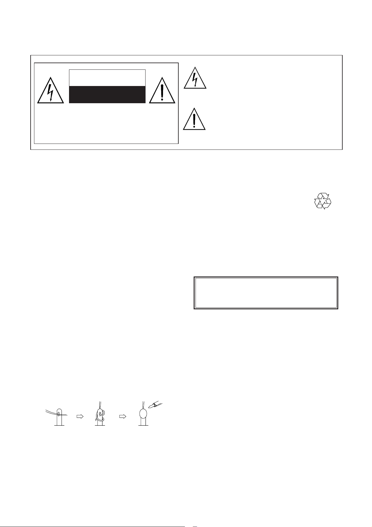
CAUTION
RISK OF ELECTRIC SHOCK
DO NOT OPEN
The lightning flash with arrowhead symbol,
within an equilateral triangle, is intended to
alert the user to the presence of uninsulated
“dangerous voltage” within the product’s enclo
sure that may be of sufficient magnitude to
constitute a risk of electric shock to persons.
CAUTION: TO REDUCE THE RISK OF
ELECTRIC SHOCK, DO NOT REMOVE COVER
(OR BACK). NO USER-SERVICEABLE PARTS
INSIDE. REFER SERVICING TO QUALIFIED
SERVICE PERSONNEL ONLY.
PRECAUTIONS DURING
SERVICING
1. In addition to safety, other parts and
assemblies are specified for conformance with
such regulations as those applying to spurious
radiation. These must also be replaced only
with specified replacements.
Examples: RF converters, tuner units, antenna
selection switches, RF cables, noise-blocking
capacitors, noise-blocking filters, etc.
2. Use specified internal Wiring. Note especially:
1) Wires covered with PVC tubing
2) Double insulated wires
3) High voltage leads
3. Use specified insulating materials for hazardous
live parts. Note especially:
1) Insulating Tape
2) PVC tubing
3) Spacers (insulating barriers)
4) Insulating sheets for transistors
5) Plastic screws for fixing micro switches
4. When replacing AC primary side components
(transformers, power cords, noise blocking
capacitors, etc.), wrap ends of wires securely
about the terminals before soldering.
5. Make sure that wires do not contact heat
generating parts (heat sinks, oxide metal film
resistors, fusible resistors, etc.)
6. Check if replaced wires do not contact sharply
edged or pointed parts.
7. Make sure that foreign objects (screws, solder
droplets, etc.) do not remain inside the set.
The exclamation point within an equilateral
triangle is intended to alert the user to the
presence of important operating and
maintenance (servicing) instructions in the
literature accompanying the appliance.
MAKE YOUR CONTRIBUTION
TO PROTECT THE
ENVIRONMENT
Used batteries with the ISO symbol
for recycling as well as small accumulators
(rechargeable batteries), mini-batteries (cells) and
starter batteries should not be thrown into the
garbage can.
Please leave them at an appropriate depot.
WARNING:
Before servicing this TV receiver, read the
SAFETY INSTRUCTION and PRODUCT
SAFETY NOTICE.
SAFETY INSTRUCTION
The service should not be attempted by anyone
unfamiliar with the necessary instructions on this
apparatus. The following are the necessary
instructions to be observed before servicing.
1. An isolation transformer should be connected in
the power line between the receiver and the
AC line when a service is performed on the
primary of the converter transformer of the set.
2. Comply with all caution and safety related
provided on the back of the cabinet, inside the
cabinet, on the chassis or picture tube.
3. To avoid a shock hazard, always discharge the
picture tube's anode to the chassis ground
before removing the anode cap.
4. Completely discharge the high potential voltage
of the picture tube before handling. The picture
tube is a vacuum and if broken, the glass will
explode.
Page 4
5. When replacing a MAIN PCB in the cabinet,
2/140
always be certain that all protective are
installed properly such as control knobs,
adjustment covers or shields, barriers, isolation
resistor networks etc.
6. When servicing is required, observe the original
lead dressing. Extra precaution should be given
to assure correct lead dressing in the high
voltage area.
7. Keep wires away from high voltage or high
tempera ture components.
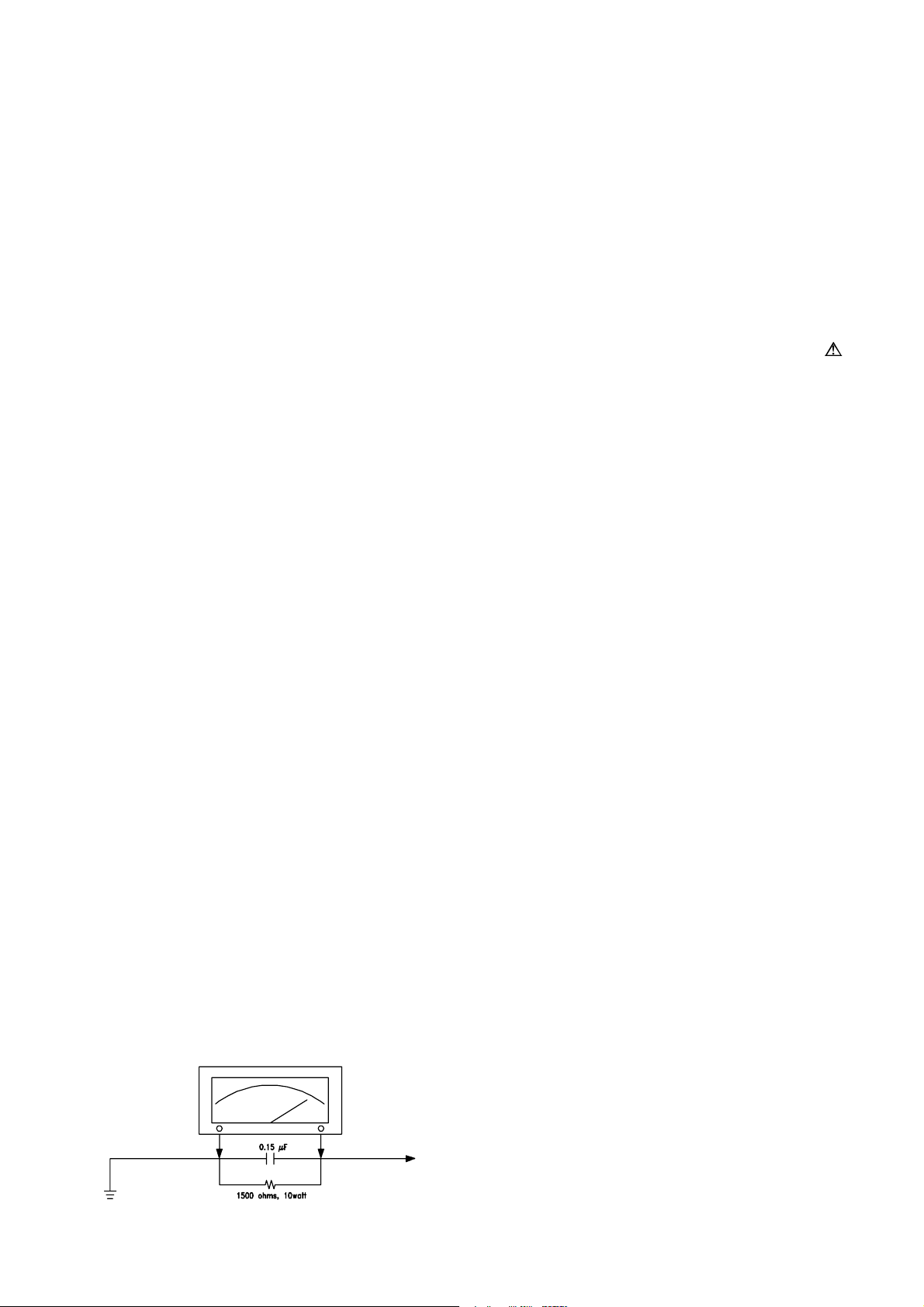
8. Before returning the set to the customer,
always perform an AC leakage current check
on the exposed metallic parts of the cabinet,
such as antennas, terminals, screwheads,metal
overlay, control shafts, etc., to be sure the set
is safe to operate without danger of electrical
shock. Plug the AC line cord directly to the
AC outlet (do not use a line isolation
transformer during this check). Use an AC
voltmeter having 5K ohms volt sensitivity or
more in the following manner.
Connect a 1.5K ohm 10 watt resistor paralleled
by a 0.15µF AC type capacitor, between a
good earth ground (water pipe, conductor etc.,)
and the exposed metallic parts, one at a time.
Measure the AC voltage across the combination
of the 1.5K ohm resistor and 0.15 uF
capacitor. Reverse the AC plug at the AC
outlet and repeat the AC voltage measurements
for each exposed metallic part.
The measured voltage must not exceed 0.3V
RMS.
This corresponds to 0.5mA AC. Any value
exceeding this limit constitutes a potential
shock hazard and must be corrected
immediately.
The resistance measurement should be done
between accessible exposed metal parts and
power cord plug prongs with the power switch
"ON". The resistance should be more than
6M ohms.
AC VOLTMETER
PRODUCT SAFETY NOTICE
Many electrical and mechanical parts in this
apparatus have special safety-related
characteristics.
These characteristics are offer passed
unnoticed by visual spection and the protection
afforded by them cannot necessarily be obtained
by using replacement components rates for a
higher voltage, wattage, etc.
The replacement parts which have these
special safety characteristics are identified by
marks on the schematic diagram and on the parts
list.
Before replacing any of these components,
read the parts list in this manual carefully. The
use of substitute replacement parts which do not
have the same safety characteristics as specified
in the parts list may create shock, fire, or other
hazards.
9. Must be sure that the ground wire of the AC
inlet is connected with the ground of the
apparatus properly.
Good earth ground
such as the water
pipe, conductor,
etc.
AC Leakage Current Check
Place this probe
on each exposed
metallic part
Page 5
Technical Specification
3/140
Product Model LCT26Z4AD
TV System NTSC M, ATSC
VIDEO System NTSC
Screen Size 26” diagonal
Active Area 575.8mm(H) x 323.7mm(V)
Aspect Ratio 16:9
External Size (with stand) 715.43 mm (W) x 554.62 mm (H) x 115.07 mm (D)
Gross Weight (with stand) 17.3 kg
Display Resolution
Pixel Pitch (Sub Pixel) 0.1405 (H) x 0.4215 (V) mm
Display Color 16.2 millions of colors (R/G/B each 256 scales)
Gray Scale 256 (R/G/B each 8-bit)
Brightness (Peak Value) 500cd/m
Contrast (Dark Room) 800:1
Sound Effect Acoustic Cinema Enhancement
Power Supply AC 120V, 60 Hz
Power Consumption 160W
Input Terminal
Output Terminal
1366 (H) x 768 (V) pixels (Each pixel has R/G/B 3 color
cells)
2
Antenna Input (F Type) x 1 (NTSC + ATSC/Clear QAM)
HDMI (Ver1.2) connector x2
VGA (D-Sub 15 Pin Type) x 1
Component Video - YPbPr x 1 RCA Terminals
Video Input RCA Terminals x 1
S-Video Input Mini Din 4 Pin Terminal x 1
Stereo, Audio x 4
1 set of Audio Output terminals (RCA, L&R)
SPDIF (Coaxial for all) x 1
SPDIF (Coaxial only for DVD) x 1
Note: The specifications shown above may be changed without notice for quality improvement.
Page 6
Support the Signal Mode
4/140
A. VGA Mode
Resolution
640 x 480 31.50 60.00
800 x 600
1024 x 768 48.40 60.00
B. YPbPr Mode
Resolution
480p(720x480) 31.468 59.94
720p(1280x720) 45.00 60.00
1080i(1920x1080) 33.75 60.00
C. HDMI Mode
Horizontal
Frequency
Vertical
Frequency
(KHz)
35.16 56.25
37.90 60.32
48.08 72.19
Horizontal
Frequency
Vertical
Frequency
(KHz)
(Hz)
(Hz)
Resolution
Horizontal
Frequency
(KHz)
Vertical
Frequency
(Hz)
480p 31.468 59.94
720p 45.00 60.00
1080i 33.75 60.00
- When the signal received by the Display exceeds the allowed range, a warning
shall appear on the screen.
- You can confirm the input signal format from the on-screen.
message
Page 7
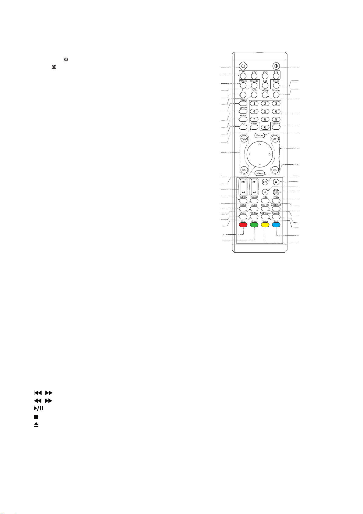
Remote Control
5/140
(Note: Details refer to AKAI TV Universal Remote Control Programming & Codes Guide.)
Standby( ): Press to turn on and off.
Mute( ): Press this button to quiet the sound.
Press again to reactivate the sound.
Press these buttons to select control of the
TV, DVD, VCR or Set-top Box device.
P. Mode: Press to cycle through the picture
modes: Cinema, Normal, Vivid, Hi-Bright and
User.
S. Mode: Press to cycle through
the sound
modes: Normal, News, Cinema, Concert and
User.
Sleep: Press repeatedly until it displays
the time in minutes (10, 20, 30,
90, 120 and Off) that you want the TV to
remain
on before shutting off. To cancel sleep
time, press Sleep button repeatedly
40, 50, 60,
until
sleep Off appears.
F1: Press to cycle through
the Stereo and
Multi-channel TV sound options: Mono,
Stereo and Bilingual.
CCD: Press to select the Closed Caption
mode.
Display: Press to display the channel
information;this information disappears after
9 seconds.
V-Chip: Select the child protect mode you want.
0~9 Number Buttons: Press 0~9 to select a channel, and input the password
Freeze: This button does not function on your TV LCT26Z4AD since it does not have
“freeze” feature.
DTV/TV: Press to choose DTV/TV (high definition channels) directly.
Guide (Digital TV Timetable): Press to display the (Digital TV Timetable) mode. Press
again to exit.
DOT: Press number buttons with it to
select the channels directly in DTV.(i.e. channel 108-1
would need the dot button after the 8)
Recall: Press to return to previous channel. (Only for TV)
Source: Press to select the signal source, such as TV, AV, S-Video, YPbPr, DVD, VGA,
HDMI 1 or HDMI 2.
Enter: Press to enter or confirm.
VOL +/-: Press to adjust the aduio levels.
CH +/- : Press to select the channel forward or backward.
∧, ∨, <, >: Press ∧, ∨, <, > to move the on-screen cursor.
Menu: Press to enter into the on-screen setup menu, press again to exit.
, : Press to skip the backward or forward.
, : Press to search the backward or forward.
: Press to play or pause the DVD disc.
: Press to stop playing the disc.
: Press to stop playing the disc.
DVD Menu: Press to return DVD disc menu.
Prog.: Press to display the program menu. Press it again to exit.
Title: Press to display to DVD disc title.
Page 8
Repeat: When in DVD mode, press to cycle
through the options: CHAPTER, TITLE, ALL
and nothing.While in CD mode, the options
are: TRACK, ALL.
Subtitle: Press to select desired DVD subtitle.
Setup: Press to display a setup page. Press
it again to exit menu.
Audio: Press to select desired audio track.
DVD Info: Press to display DVD information.
Angle/Exit: Press this button to select desired
viewing angle of the Video (disc feature).
Favorite: Press to select the favorite channel
from list.
Add/Erase: Press to add or delete favorite
channels.
Pic Size: Press to change the screen size, such
as Full, 4:3.(Note: When in VGA mode, it can
only select “Full”.)
Zoom: This button is not in use.
Red: This is a special control function for the
Digital tuner.
Green: This is a special control function for the
Digital tuner.
Yellow: This is a special control function for the
Digital tuner.
Blue: This is a special control function for the
Digital tuner.
6/140
Page 9
POWER BOARD
7/140
DTVS205CH201A
Digital/Analog
Tuner
HDMI1
HDMI2
CVBS/SIF
Two to one
HDMI Switch
TMDS
MT5112BD
DTV Demodulator
10Bit LVDS
k
TS Doc
LCD panel
MAIN BOARD
Coaxial
Output
COAXIAL
5V
Standby 5V
12V
9V
24VA (For Class D)
COMB DVD
Am5888
SL/F
Motor
Driver
Loader
&Optical
Pick up
Comp
DVD
VGA
AV
S-Video
Audio
X4
MT5370
ADC
Scaler
ATSC
LVDS Transfer
IIS
CE2836
Audio
ADC&DAC
R2S15102
Class D
24C16
EEPROM
Flash
32M
NJRC4558
Audio Buffer
DDR
256M
Max232
Level Shift
Audio
Output
RS232
Socket
To HET-4052
To QS3VH257
4334KSZ
Audio DAC
MT1389
MPEG decoder
&Servo System
EEPROM
SDRAM
64M
Flash
16M
Amplifier
Relay
Speaker
Page 10
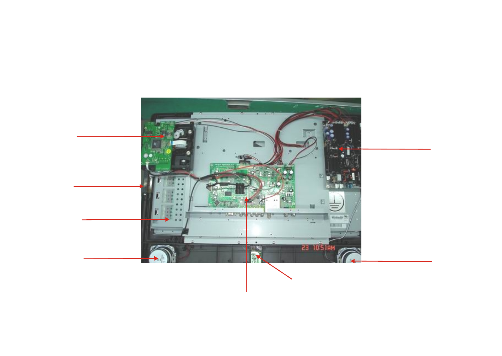
DVD
8/140
Key Board
Inverter Board
Parts Position
Power Board
Skeaper
Skeaper
IR Board
Main Board
Page 11
A
9/140
B
C
D
E
MT5372RAV6
MT5372 (PBGA) REFERENCE DESIGN - 4 LAYERS
DV33
AMP_GND
+24V
+9V
+12V
+5V
+5VSB
DV33SB
GND
AGND_PLL
AGND_AFE
AGND_HDMI
AGND_LVDS
OPWRSB
OPCTRL0
OPCTRL1
OPCTRL2
OPCTRL3
OPCTRL4
OIRI
GPIO_58
GPIO_59
GPIO_70
GPIO_[71..84]
GPIO_130
GPIO_131
GPIO_132
GPIO_133
ADD2
ADD1
IR
OPCTRL0
OPCTRL2
H3
HOLE/GND/NC
H/H4.0-D8.0
1
1
H4
HOLE/GND/NC
HOLE
1
1
Drawn:
Checked:
D54
MARK
D59
MARK
2
3
4
5
2
3
4
5
2
3
4
5
2
3
4
5
<Designer>
<Checker>
114Thursday, March 01, 2007
D55
MARK
Rev
1
of
9
9
8
8
7
7
6
6
9
9
8
8
7
7
6
6
D53
MARK
D58
MARK
H2
HOLE/GND/NC
H/H4.0-D8.0
9
8
7
6
1
1
DV332,4,5,6,7,11,12,13,14
AMP_GND12
+24V12
+9V2,11
+12V13
+5V2,7,8,9,11,13
+5VSB2,7,10,11,12,13,14
DV33SB2,5,6,7,10,11,12,13
GND2,3,4,5,6,7,8,9,10,11,12,13,14
AGND_PLL2,3,4,5,6,7,8,9,10,11,12,13,14
AGND_AFE2,3,4,5,6,7,8,9,10,11,12,13,14
AGND_HDMI2,3,4,5, 6,7,8,9,10,11,12,13,14
AGND_LVDS2,3,4,5,6,7,8,9,10,11,12,13,14
AGND_LVDS2,3,4,5,6,7,8,9,10,11,12,13,14
GLOBAL POWER
OPWRSB5
OPCTRL05
OPCTRL15
OPCTRL25
OPCTRL35,12
OPCTRL45,13
OIRI5
GPIO_585
GPIO_595
GPIO_705
GPIO_[71..84]5
GPIO_1305
GPIO_1315
GPIO_1325
GPIO_1335
ADD213
ADD113
IR7
OPCTRL05
OPCTRL25
2
2
3
3
4
4
5
5
Rev DATEHistory
RA-V0 INITIAL VERSION 2006/07/14
4 4
RA-V1 2006/07/31
RA-V2
3 3
01.INDEX
OPCTRL4
RA-V1
02.POWER
03.TUNER
ASIC04.MT5112
05.MT5372 ASIC
GPIO DEPEND-ON YO UR APPLICATION
WORKABLE IN STANDBY AND NORMAL MODE
06.MT5372 BYPASS CAP.
07.MT5372 PERIPHERAL
08.DDR1
09.YPBPR
10.HDMI
2 2
11.AUDIO
12.AUDIO
MEMORY
INPUT
/VGA INPUT
CODEC
AMP
GPIO_70
TP1
GPIO_70
GPIO_130
TP2
GPIO_130
GPIO_131
TP3
GPIO_131
GPIO_132
TP4
GPIO_132
GPIO_133
TP5
GPIO_133
GPIO DEPEND-ON YO UR APPLICATION
WORKABLE IN NORMAL MODE ONLY
RA-V1
J1
1
2
3
4
5
6
7
R. ANGLE
8
9
10
11
12
12P2.54mm
DIP12/W/H/P2.54
VS_ON
SYS_PWRSYS_PWRSYS_PWRSYS_PWRSYS_PWRSYS_PWRSYS_PWRSYS_PWRSYS_PWRSYS_PWRSYS_PWRSYS_PWRSYS_PWRSYS_PWRSYS_PWRSYS_PWRSYS_PWRSYS_PWRSYS_PWRSYS_PWRSYS_PWRSYS_PWRSYS_PWRSYS_PWRSYS_PWRSYS_PWRSYS_PWRSYS_PWRSYS_PWRSYS_PWRSYS_PWRSYS_PWR
+5V
CB1
1000pF/NC
C0603/SMD
+9V
+5V
+5VSB
RA-V1
+9V
220uF/16V
100UF/220UF/SMD
VS_ON
Only for PDP
SYS_PWR
R11
0R/NC
R0603/SMD
J2
DIP8/W/H/P2.54
8P2.54mm
1
2
3
4
5
6
7
8
POWER INPUT
+9V
+
CE2
R0603/SMD
+9V
+12V
ADD1
R0603/SMD
R4
0R/NC
R0603/SMD
AMP_GND
4.7K/NC
+5VSB
3 2
+24V
CB2
0.1uF
C0603/SMD
DV33SB
R1
R6
0R/NC
R8
1K
R0603/SMD
1
Q2
2N3904
SOT23/SMD
100UF/220UF/SMD
Q1
2N3904/NC
SOT23/SMD
ADD2
DV33SB
+5V
+
CE1
220uF/16V
+5VSB
R2
1K/NC
R0603/SMD
1
3 2
R9
4.7K/NC
R0603/SMD
R12
4.7K
R0603/SMD
CE3
470uF/16V
C470UF16V/D8H9G
CB3
0.1uF
C0603/SMD
DV33SB
R5
1K/NC
OPCTRL4
R0603/SMD
R7
10k/NC
R0603/SMD
DV33SB
OPWRSB HIGH :POWER OFF
OPWRSB LOW :POWER ON
R10
NC
R0603/SMD
OPWRSB
R13
10K
R0603/SMD
+12V
+
CB4
0.1uF
C0603/SMD
R3
10K
R0603/SMD
HOLE/GND/NC
H/H4.0-D8.0
9
9
8
8
7
7
6
6
H1
9
2
2
3
4
5
1
1
8
3
7
4
6
5
DEVICETYPENAME
+24V
+12V
+5V
+5VSB
DV33SB
+5V_TUENR
DV33_DM
DV18_DM
DV33
AV33
DV18_DDR
AV15
DV12
1 1
AV12
GND
AGND_PLL
AGND_AFE
AGND_HDMI
AGND_LVDS
POWER +24V
POWER +12V
POWER +5V
POWER +5V
POWER +3.3V
POWER +5V
POWER +3.3V
POWER +1.6V
POWER +3.3V
POWER +3.3V
POWER +1.8V
POWER +1.5V
POWER +1.2V
POWER +1.2V
GROUND
GROUND
GROUND
GROUND
GROUND
A
POWER SUPPLY
POWER SUPPLY
POWER SUPPLY
POWER SUPPLY
STANDBY POWER
TUNER POWER
MT5112 POWER AND ITS PERIPHERAL
MT5112 POWER
MT5372 POWER AND ITS PERIPHERAL
MT5372 ANALOG POWER
MT5372 DDR POWER
MT5372 VIDEO FRONT-END POWER
MT5372 POWER
MT5372 ANALOG POWER
DIGITAL GROUND
ANALOG GROUND
ANALOG GROUND
ANALOG GROUND
ANALOG GROUND
DV33SB
RA-V3
+5VSB
R15
10K
R21
32
R22
+5V
4.7K
R25
510
R0603/SMD
LED_GRE
R20
NC
R0603/SMD
Q3
1
2N3906
LED_RED
R24
510
R375
10K
20K/NC
OIRI
ADC KEY & GPIO KEY KEYPAD
B
C
DV33
KEYPAD
R1610K
R1910K
R1810K
R1710K
10K R14
R23 0
+5VSB
RA-V3
GPIO_71 SOURCE
L1 FB/70R500mA/0603
GPIO_72
GPIO_74
GPIO_73
OPCTRL0
MENU
L2 FB/70R500mA/0603
VOL-
L3 FB/70R500mA/0603 CB8 1000pF
VOL+
L4 FB/70R500mA/0603
CH+
L5 FB/70R500mA/0603
CH-OPCTRL2
L6 FB/70R500mA/0603
IR
STANDBYOPCTRL1
L7 FB/70R500mA/0603
+5VSB_IR
R26
0
CB5 1000pF
CB6 1000pF
CB7 1000pF
CB9 1000pF
CB10 1000pF
CB11 100pF
CB12 1000pF
CB13 1000pF
CB14 1000pF
CB15 1000pF
D
SOURCE
MENU
VOLVOL+
CHCH+
IR
LED_RED
LED_GRE
STANDBY
+5VSB_IR
J3
1
2
3
4
5
6
7
8
9
10
11
12
13
13P2.0mm
DIP13/w/h/p2.0
H6
HOLE/GND/NC
H/H4.0-D8.0
1
D51
MARK
D56
MARK
INDEX
MT5371_V07
2
2
3
3
4
4
5
5
1
D52
MARK
D57
MARK
E
9
9
8
8
7
7
6
6
ZhongShan KAWA Electronic Inc.
Title
Document Number
Size
Custom
Date: Sheet
Page 12

A
10/140
B
C
D
E
+9V
+
CE4
220uF/16V
100UF/220UF/SMD
4 4
+5V_TUNER
CE10
+
220uF/16V
100UF/220UF/SMD
U1
3
IN
CB16
0.1uF
C0603/SMD
H5
RADIATOR
SANRE
CB24
0.1uF
C0603/SMD
Regulator AP1522 SOT23-5/SMD
OUT
ADJ/GND
L7805
1
TO220/DIP/SU
L12
10uH
L/IND/SMD/0805
5
V_IN
GND
4
AP1522
2
U3
SW
FB3SHDN
+5V_TUNER
CE5
+
220uF/16V
100UF/220UF/SMD
CB17
0.1uF
C0603/SMD
POWER SUPPLY +5V FOR TUNER
D2
2
3
1
DIODE SMD FHBAS40
FHBAS40
1
2
R33
5.6K
R0603/SMD
Ra
CB26
0.1uF/50V
C0603/SMD
+30V_TUNER
R31
47K
R0603/SMD
R32
82K
R0603/SMD
Rb
12
CE9
+
22uF/50V
100UF/220UF/SMD
RA-V1
CB23
0.1uF/50V
C0603/SMD
U2
CB18
0.1uF/NC
C0603/SMD
4
Vcc
3
OCSET
AP1513/SOP-8
AP1513
EN
2
+5V DV12
L9
FB/75R/1A/0805
BEAD/SMD/0805
CE6
220uF/16V
100UF/220UF/SMD
CB20
+
0.1uF
C0603/SMD
R29
100K
R0603/SMD
R27
3K
R0603/SMD
O/P
O/P
Vss7Vss
8
CB22
0.1uF
C0603/SMD
FB
1000mA
6
5
1
RA-V3
L10
LTRH104R-270
S-LF125M
D1
B340A/3A/SMA
B320A
CB19
0.1uF/NC
C0603/SMD
R28
1.2K
R0603/SMD
R30
2K
R0603/SMD
CE7
+
220uF/16V
100UF/220UF/SMD
L8
FB/75R/1A / 0805
BEAD/SMD/0805
L11
FB/75R/1A / 0805
BEAD/SMD/0805
0.8 x (1+1.2 K/2K) = 1.28V
POWER +1V2 FO R M T5 372 (DIGITAL)
L13
FB/75R/1A/ 0805
BEAD/SMD/0805
AV12
POWER +1V2 FOR MT5372 (ANALOG)
720mA
CB21
0.1uF
C0603/SMD
41mA
CB25
0.1uF
C0603/SMD
CE8
+
220uF/16V
100UF/220UF/SMD
CE11
+
100uF/16V
100UF/220UF/SMD
Vout = 1.25 x ( 1 + Rb / Ra )
POWER SUPPLY +30V FOR SAMSU NG T UNER
+5V
3 3
CE12
+
220uF/16V
100UF/220UF/SMD
3
CB27
0.1uF
C0603/SMD
U4
OUT
ADJ/GND
AMS1084/ADJ
1
TO-252-3/SMD
CB433
4.7uF/6.3V
C0603/SMD
2
R34
110
R0603/SMD
R35
180
R0603/SMD
CE13
+
100uF/16V
100UF/220UF/SMD
RA-V3
CB28
0.1uF
C0603/SMD
IN
L14
FB/70R/500mA/0603
BEAD/SMD/0603
POWER SUPPL Y +3 V3 (DIGITAL) FOR M T5372
L17
FB/75R/1A/ 0805
BEAD/SMD/0805
L18
FB/75R/1A/0805/NC
BEAD/SMD/0805
DV33
AV33
CB29
0.1uF
C0603/SMD
CB35
0.1uF
C0603/SMD
28mA
390mA
CB30
4.7uF/6.3V
C0603/SMD
CE15
+
100uF/16V
100UF/220UF/SMD
POWER +3V3 FOR MT5372 (ANALOG)
U5
AP1513/SOP-8
AP1513
4
2 2
1 1
CE17
220uF/16V
100UF/220UF/SMD
+5VSB
CE22
+
220uF/16V
100UF/220UF/SMD
+
CB41
0.1uF
C0603/SMD
CB45
0.1uF
C0603/SMD
3
L20
FB/75R/1A/ 0805
BEAD/SMD/0805
R37
3K
R0603/SMD
R39
100K
R0603/SMD
U7
2
OUT
IN
ADJ/GND
AMS1117-3.3V
1
SOT223/SMD
CB38
0.1uF/NC
C0603/SMD
Vcc
3
OCSET
2
CE23
+
100uF/16V
100UF/220UF/SMD
EN
O/P
O/P
Vss7Vss
8
CB42
0.1uF
C0603/SMD
CB46
0.1uF
C0603/SMD
900mA
6
5
1
FB
L23
FB/75R/1A/0805
BEAD/SMD/0805
RA-V3
L21
LTRH104R-220
S-LF125M
D3
B340A/3A/SMA
B320A
CB39
0.1uF/NC
C0603/SMD
R38
1.2K
R0603/SMD
R40
1K
R0603/SMD
0.8 x (1+1K/1K) = 1.6V
POWER SUPPLY +1V6 FOR MT5112
DV33SB
25mA
CE24
+
100uF/16V
100UF/220UF/SMD
CE16
+
220uF/16V
100UF/220UF/SMD
1.25 x (1+1 80/110) = 3.3V
STANDBY POWER +3V3 FOR MT5372
A
B
710mA
DV18_DM+5V
CB40
0.1uF
C0603/SMD
POWER SUPPLY +3V3 FOR MT5112
CE18
+
220uF/16V
100UF/220UF/SMD
CB43
0.1uF
C0603/SMD
RA-V2
U6
3
IN
OUT
ADJ/GND
AMS1084
1
TO-252-3/SMD
CB434
4.7uF/6.3V
C0603/SMD
2
R41
CE19
+
100uF/16V
110
R0603/SMD
100UF/220UF/SMD
RA-V2
R42
120
R0603/SMD
1.25 x (1+1 20/110) = 2.6V
L22
FB/75R/1A/ 0805
BEAD/SMD/0805
CB44
0.1uF
C0603/SMD
POWER +1V8 FOR MT5372 / DDRII
AV33 AV15
CE25
+
220uF/16V
100UF/220UF/SMD
RA-V2
C
CB47
0.1uF
C0603/SMD
4.7uF/6.3V
C0603/SMD
CB435
U8
3
2
OUT
IN
ADJ/GND
1
AMS1117/adj
SOT223/SMD
R0603/SMD
CE26
R43
+
100uF/16V
110
R0603/SMD
100UF/220UF/SMD
R44
22
1.25 x (1+22/110) = 1.5V
CB48
0.1uF
C0603/SMD
POWER +1V5 FOR VIDE O FRONT-END1
D
DV26_DDR+5V
RA-V1
CE20
+
100uF/16V
100UF/220UF/SMD
RA-V2
88mA
L19
FB/70R/500mA/0603
BEAD/SMD/0603
80mA
DV33_DM
CB37
CB36
4.7uF/6.3V
0.1uF
C0603/SMD
C0603/SMD
+5V_TUNER3
DV125,6
+9V1,11
+12V1,13
+5V1,7,8,9,11,13
+5VSB1,7,10,11,12,13,14
+30V_TUNER3
DV33_DM3,4
DV18_DM4
DV331,4,5,6,7,11,12,13,14
AV336,10,11
DV26_DDR5,6,8
AV156
AV125,6
DV33SB1,5,6,7,10,11,12,13
GLOBAL POWER
GND1,3,4,5,6,7,8,9,10,11,12,13,14
AGND_AFE1,3,4,5,6,7,8,9,10,11,12,13,14
AGND_LVDS1,3,4,5,6,7,8,9,10,11,12,13,14
AGND_PLL1,3,4, 5,6,7,8,9, 10,11,12,13,14
ZhongShan KAWA Electronic Inc.
Title
POWER
Document Number
Size
Custom
MT5371_V07
Date: Sheet
+5V_TUNER
DV12
+9V
+12V
+5V
+5VSB
+30V_TUNER
DV33_DM
DV18_DM
DV33
AV33
DV26_DDR
AV15
AV12
DV33SB
GND
AGND_AFE
AGND_LVDS
AGND_PLL
Drawn:
Checked:
E
<Designer>
<Checker>
214Thursday, Ma rch 01, 2007
Rev
2
of
Page 13
A
11/140
B
C
D
E
+30V_TUNER2
DV33_DM2,4
GND1,2,4,5,6,7,8,9,10,11,12,13,14
IF_AGC4
4 4
FAT_IN+4
FAT_IN-4
TUNER_SCL14
TUNER_SDA14
TUNER INTERFACE
CVBS05
MPX15
MPX25
AGND_AFE1,2,4,5,6,7,8,9,10,11,12,13,14
+30V_TUNER
DV33_DM
GND
IF_AGC
FAT_IN+
FAT_INTUNER_SCL1
TUNER_SDA1
CVBS0
MPX1
MPX2
AGND_AFE
AGND_AFE1,2,4,5,6,7,8,9,10,11,12,13,14
+5V_TUNER2
CVBS25,9
CVBS35,9
SY05,9
SC05,9
SY15,9
SC15,9
SY25,9
SC25,9
AV / SV VIDEO INPUT
AGND_AFE
+5V_TUNER
CVBS2
CVBS3
SY0
SC0
SY1
SC1
SY2
SC2
TUNER - ANALOG OUTPUT
+5V_TUNER
R48
10K/NC
R0603/SMD
ADIN3
R49
10K/NC
R0603/SMD
32
QF1
2N7002/NC
SOT23/SMD
1
32
QF2
2N7002/NC
SOT23/SMD
1
Only for Philips Tuner
DV33_DM
TUNER_SDA1
TUNER_SCL1
RA-V3
R400
CB49
0.1uF/NC
C0603/SMD
R46 N C
R47 N C
R50
4.7K/NC
R0603/SMD
0/NC
R0603/SMD
R0603/SMD
R0603/SMD
CB51
0.1uF/NC
C0603/SMD
5V_TU
PHILIPS COMBO-TUNER
CB50
10nF/NC
C0603/SMD
R51
0R/NC
R0603/SMD
R52
0R/NC
R0603/SMD
ROUTE SYMMETRICALLY
R45
4.7K/NC
R0603/SMD
FAT_IN+
FAT_IN-
TUNER_SCLO
TUNER_SDAO
IF_AGC
No Install
CB52
1000pF
C0603/SMD
RA-V1
MPX2
MONO
U9
15
GND
16
GND
IF AGC
AS TUNER
2ND IF SOUND
CVBS
+5V IF
AF/MPX
1
2
NC
3
+5V
L24 2.2uH/NC BEAD/SMD/0603
4
SCL
L25 2.2uH/NC BEAD/SMD/0603
5
SDA
6
7
DIF
8
DIF
AS
9
10
AS IF
SIF
11
NTSC_CVBS
12
5V_TU
13
MONO
14
17
GND
18
GND
5V_PH
AGC MONITOR (NC)
3 3
PORT TUNER FQD1236/F H-5/NC
MK5
ADIN35
TUNER_SDAO
TUNER_SCLO
SIF LEVEL SHIFTER
U10
2 2
PORT TUNER DTVS205CH201A
1 1
RG_AGC_TP
VT(+30V)
IF_AGC
TUNER_IF_TP
BP(+5V)
CVBS
TH1
GND
TH2
GND
1
NC
2
NC
3
NC
4
NC
5
NC
6
NC
7
8
NC
9
10
IF+
11
IF-
12
13
C0603/SMD
14
SCL
15
SDA
16
GND
17
18
NC
19
AFT
20
SIF
21
TH3
GND
TH4
GND
TH5
GND
TH6
GND
TH7
GND
TH8
GND
R404
R0603/SMD
5V_TU
AFT
SIF
NTSC_CVBS
AS
0
A
CB56
NC
5V_PH
RA-V2
R399
0
R0603/SMD
CB54
100p
C0603/SMD
RA-V3
CB63
470P
C0603/SMD
RA-V3
CB55
0.1uF
C0603/SMD
CB61
NC
C0603/SMD
RA-V1
L26
FB/70R/500mA/0603
BEAD/SMD/0603
CB64
0.1uF
C0603/SMD
SAMSUNG COMBO-TUNER
+30V_TUNER
RA-V3
CB62
NC
C0603/SMD
L27
FB/75R/1A/0805
+
CE29
BEAD/SMD/0805
470uF/16V
C470UF16V/D8H9G
+5V_TUNER
FAT_IN+
R55
0
R0603/SMD
FAT_IN-
R57
0
R0603/SMD
ROUTE SYMMETRICALLY
CB58
100p
C0603/SMD
R63
100
R64
100
R0603/SMD
R0603/SMD
CB59
10nF
C0603/SMD
B
IF_AGC
R59
4.7K
R0603/SMD
Close to Tuner
TUNER_SCL1
TUNER_SDA1
RA-V2
NTSC_CVBS
R58
100
R0603/SMD
1
SIF
RA-V3
+5V_TUNER
NEARLY TUNER NEARLY MT5372
R54
10
R0603/SMD
+
CE28
47uF/16V
100UF/220UF/SMD
Q5
2N3904
SOT23/SMD
3 2
R60
RA-V3
R0603/SMD
R401
0/NC
R0603/SMD
C
R0603/SMD
R396
4.7K
CB60
47pF
10
C0603/SMD
R62
75R/1206
R1206/SMD
NTSC_SIF
CB436
10nF
C0603/SMD
R61
100
R0603/SMD
R67
0
R0603/SMD
CB57
47nF
C0603/SMD
CB65
5.6pF
C0603/SMD
CB66
15pF
C0603/SMD
SIF (4.5MHz)
CVBS0
NTSC CVBS
MPX1
AFT ADIN3
R53
100K
R0603/SMD
R56
220K
R0603/SMD
TUNER_SDA1
TUNER_SCL1
D
NEARLY MT5372NEARLY TUNER
CB53
0.1uF
C0603/SMD
DV33_DM
R65
R66
4.7K
4.7K
R0603/SMD
R0603/SMD
ZhongShan KAWA Electronic Inc.
Title
TUNER
Document Number
Size
Custom
MT5371_V07
Date: Sheet of
Drawn:
E
Checked:
<Designer>
<Checker>
314Thursday, March 01, 2007
Rev
1
Page 14
A
12/140
B
C
D
E
DVDD33
DVDD33
61
60
DGND33
ANT_TX(POUT3.1)
ADVDD33_2
59
58
DVDD33
ANT_RX(PIN3.0)
DVDD33
DVDD18
DVDD18
DVDD33
RESERVE HEAT-SINK SPACE
GPIO_0
DV33
R71
4.7K
R0603/SMD
RN1
1 2
3 4
5 6
7 8
33x4
RN0603/SMD
RN2
1 2
3 4
5 6
7 8
33x4
RN0603/SMD
DV33
R376
NC
R0603/SMD
GPIO_18
TS0VALID
TS0CLK
TS0SYNC
TS0DATA0
TS0DATA1
TS0DATA2
TS0DATA3
RA-V3
TUNER_SDA TUNER_SDA1
TUNER_SCL TUNER_SCL1
MODIFY IN RAV2
51
DVDD33
DGND33
GPIO1(P1.1)
RESET_
HOST_CLK
DGND18
DVDD18
DGND33
DVDD33
DGND18
DVDD18
TS_ERR
TS_VAL
TS_CLK
DGND33
DVDD33
TS_SYNC
TS_DATA0
TS_DATA1
DGND18
DVDD18
TS_DATA2
TS_DATA3
DGND33
DVDD33
25
RN3
33x4
RN0603/SMD
7 8
U11
MT5112AD_BD/TQFP100
50
NC
49
48
47
46
45
44
43
42
41
40
39
38
37
36
35
34
33
32
31
30
29
28
27
26
SIF_SCL
SIF_SDA
DVDD33
DVDD18
DVDD33
DVDD18
DVDD33
DVDD18
53
57
54
56
55
52
NC
DVDD18
DGND18
GPIO3(P1.3)
GPIO2(P1.2)
ANT_DET(PIN3.1)
HOST_DATA
1 2
3 4
5 6
DVDD18
DVDD33
DVDD18
4 4
FAT_IN-
FAT_IN+
3 3
CB68
10nF
C0603/SMD
CB70
10nF
C0603/SMD
MT5112_IF_AGC
CB71 0.1uF
CB72 0.1uF
CB74 0.1uF
Y1
25MHz
CRYS/DIP/SMD
R70
1K
R0603/SMD
L28
220nH/NC
L/IND/SMD/0805
C0603/SMD
C0603/SMD
C0603/SMD
DVDD18
R72
1M
R0603/SMD
IF_AGC
CB67
47nF
C0603/SMD
CLOSE TO MT5112
CB69
47pF/NC
C0603/SMD
CB73
10uF/16v
C0805/SMD
L29
FB/70R/500mA/0603
BEAD/SMD/0603
CB76
18pF
C0603/SMD
CB77
18pF
C0603/SMD
CB75
0.1uF
C0603/SMD
ADVDD33_1
AVDD33
AVDD33
REFBOT
VCMEXT
REFTOP
AVDD33
AVDD3
AVDD33
XTAL2
XTAL1
AVDD33
TUNER_SDA
TUNER_SCL
MT5112_IF_AGC
R68 4.7K
R69 4.7K
72
69
73
71
75
70
IF_AGC
DVDD18
DVDD33
DGND1874RF_AGC
76
ADVDD33
77
NC
78
NC
79
AVSS8
80
AVDD8
81
IN-
82
IN+
83
AVDD1
84
NC
85
AVSS1
86
REFBOT
87
VCMEXT
88
REFTOP
89
AVSS7
90
AVDD18
91
AVDD7
92
AVDD3
93
AVDD6
94
AVSS3
95
AVSS6
96
XTAL2
97
XTAL1
98
AVSS4
99
AVDD4
100
AVSS2
101
GND
DGND33
TUNER_CLK
NC1NC2AVDD23NC4NC5NC6AVSS97NC8NC9AVDD910AVSS511AVDD512NC13NC14ADVDD3315DGND3316DVDD3317DVDD1818DGND1819NC20GPIO0(P1.0)21TS_DATA722TS_DATA623TS_DATA524TS_DATA4
AVDD33
62
65
63
64
68
66
SA167SA0
DVDD18
DGND18
DGND18
TUNER_DATA
MT5112AD/BD
TQFP-100
AVDD33
AVDD5
DV33_DM2,3
DV18_DM2
GND1,2,3,5,6,7,8,9,10,11,12,13,14
GLOBAL SIGNAL
IF_AGC3
FAT_IN+3
FAT_IN-3
TUNER_SCL13
TUNER_SDA13
TUNER INTERFACE
TS0DATA[0..7]5
TS0SYNC5
TS0VALID5
TSCLK5
GPIO_185
TS INPUT
SIF_SDA7,11
SIF_SCL7,11
GPIO_05
DV331,2,5,6,7,11,12,13,14
DV33_DM
DV18_DM
GND
IF_AGC
FAT_IN+
FAT_IN-
TUNER_SCL1
TUNER_SDA1
TS0DATA[0..7]
TS0SYNC
TS0VALID
TS0CLK
GPIO_18
SIF_SDA
SIF_SCL
GPIO_0
DV33
TS0DATA7
TS0DATA6
TS0DATA5
2 2
L30
FB/75R/1A/0805
BEAD/SMD/0805
DV18_DM
DV33_DM
1 1
L31
FB/75R/1A/0805
BEAD/SMD/0805
L34
FB/75R/1A/0805
BEAD/SMD/0805
L36
FB/75R/1A/0805
BEAD/SMD/0805
A
CB85
4.7uF/6.3V
C0603/SMD
CB96
4.7uF/6.3V
C0603/SMD
CB105
4.7uF/6.3V
C0603/SMD
DVDD18
CB86
4.7uF/6.3V
C0603/SMD
DVDD33
CB97
4.7uF/6.3V
C0603/SMD
CB106
4.7uF/6.3V
C0603/SMD
DVDD18
DVDD33
AVDD33DV33_DM AVDD33
CB79
CB78
0.1uF
0.1uF
C0603/SMD
C0603/SMD
CB91
CB92
0.1uF
0.1uF
C0603/SMD
C0603/SMD
CB100
CB101
0.1uF
0.1uF
C0603/SMD
C0603/SMD
Analog 3.3V Bypass Caps
CB81
CB80
0.1uF
0.1uF
C0603/SMD
C0603/SMD
Digital 1.8V Bypass Caps
CB94
CB93
0.1uF
0.1uF
C0603/SMD
C0603/SMD
Digital 3.3V Bypass Caps
CB102
CB103
0.1uF
0.1uF
C0603/SMD
C0603/SMD
B
CB82
0.1uF
C0603/SMD
CB95
0.1uF
C0603/SMD
CB104
0.1uF
C0603/SMD
CB83
0.1uF
C0603/SMD
AVDD33 AVDD3
CB84
0.1uF
C0603/SMD
AVDD33 AVDD5
AVDD33 ADVDD33_1
AVDD33 ADVDD33_2
TS0DATA4
L32
FB/70R/500mA/0603
BEAD/SMD/0603
L33
FB/70R/500mA/0603
BEAD/SMD/0603
L35
FB/70R/500mA/0603
BEAD/SMD/0603
L37
FB/70R/500mA/0603
BEAD/SMD/0603
C
CB87
0.1uF
C0603/SMD
CB89
0.1uF
C0603/SMD
CB98
0.1uF
C0603/SMD
CB107
0.1uF
C0603/SMD
CB88
4.7uF/6.3V
C0603/SMD
CB90
4.7uF/6.3V
C0603/SMD
CB99
4.7uF/6.3V
C0603/SMD
CB108
4.7uF/6.3V
C0603/SMD
ZhongShan KAWA Electronic Inc.
Title
MT5112 ASIC
Document Number
Size
Custom
MT5371_V07
D
Date: Sheet
Drawn:
<Designer>
Checked:
<Checker>
E
Rev
1
of
414Thursday, March 01, 2007
Page 15
5
13/140
TP17
GPIO_14
GPIO_9
GPIO_13
GPIO_10
GPIO_8
GPIO_7
GPIO_5
GPIO_4
GPIO_6
GPIO_12
GPIO_3
GPIO_1
GPIO_2
GPIO_0
B12
U12
D D
RA0
D1
RA0
RA1
A2
RA1
RA2
D2
RA2
RA3
B4
RA3
RA4
C1
RA4
RA5
A3
RA5
RA6
C2
RA6
RA7
B5
RA7
RA8
B1
RA8
RA9
A4
RA9
RA10
B3
RA10
RA11
B2
RA11
RA12
A5
RA12
RA13
A1
RA13
RWE#
D3
RWE_
RCAS#
C5
RCAS_
RRAS#
C4
RRAS_
RCS#
D5
RCS_
RCKE
E1
RCKE
RCLK0
L1
RCLK0
RCLK0#
L2
RCLK0_
RCLK1
A11
RCLK1
RCLK1#
B11
RCLK1_
RBA0
D4
RBA0
RBA1
C3
RBA1
E2
RODT
RVREF
D8
RVREF
RVREF
F4
RVREF
RESTUP
L4
REXTUP
RESTDN
M1
REXTDN
RDQS0
G1
RDQS0
G2
RDQS0_
RDQM0
F3
RDQM0
RDQ0
G4
RDQ0
RDQ1
F1
RDQ1
RDQ2
H1
RDQ2
RDQ3
E4
RDQ3
RDQ4
E3
RDQ4
RDQ5
H2
RDQ5
RDQ6
C C
B B
TP39
TP40
TP41
TP43
A A
RDQ7
RDQS1
RDQM1
RDQ8
RDQ9
RDQ10
RDQ11
RDQ12
RDQ13
RDQ14
RDQ15
RDQS2
RDQM2
RDQ16
RDQ17
RDQ18
RDQ19
RDQ20
RDQ21
RDQ22
RDQ23
RDQS3
RDQM3
RDQ24
RDQ25
RDQ26
RDQ27
RDQ28
RDQ29
RDQ30
RDQ31
POCE0#
POOE0#
POWE#
PDD0
PDD1
PDD2
PDD3
PDD4
PDD5
PDD6
PDD7
PDA0
PDA1
PDA2
PDA3
PDA4
PDA5
PDA6
PDA7
PDA8
PDA9
PDA10
PDA11
PDA12
PDA13
PDA14
PDA15
PDA16
PDA17
PDA18
PDA19
PDA20
PDA21
PDA22
EXT_MCLK
EXT_BCLK
EXT_LRCK
EXT_DATA
F2
RDQ6
G3
RDQ7
J4
RDQS1
J3
RDQS1_
K1
RDQM1
K3
RDQ8
J1
RDQ9
K4
RDQ10
H4
RDQ11
H3
RDQ12
L3
RDQ13
J2
RDQ14
K2
RDQ15
B10
RDQS2
A10
RDQS2_
C10
RDQM2
C9
RDQ16
C11
RDQ17
B9
RDQ18
D11
RDQ19
A12
RDQ20
A9
RDQ21
D10
RDQ22
D9
RDQ23
B7
RDQS3
A7
RDQS3_
C7
RDQM3
C6
RDQ24
A8
RDQ25
B6
RDQ26
B8
RDQ27
C8
RDQ28
A6
RDQ29
D7
RDQ30
D6
RDQ31
U3
POCE0_
U1
POCE1_
T4
POCE2_
U2
POOE0_
AC1
POWE_
V1
PDD0
V2
PDD1
V3
PDD2
V4
PDD3
W1
PDD4
W2
PDD5
W3
PDD6
W4
PDD7
Y1
PDA0
U4
PDA1
AE3
PDA2
AE2
PDA3
AE1
PDA4
AD4
PDA5
AD3
PDA6
AD2
PDA7
AD1
PDA8
AB2
PDA9
AB1
PDA10
AA4
PDA11
AA3
PDA12
AA2
PDA13
AA1
PDA14
Y4
PDA15
Y3
PDA16
Y2
PDA17
AC4
PDA18
AC3
PDA19
AB3
PDA20
AB4
PDA21
AC2
PDA22
P3
PDCTRLVPP
N1
PDVS1
P4
PDVS2
T3
PDENPOD
M3
PDCE1_
M4
PDCE2_
N2
PDOE_
P1
PDWE_
P2
PDIREQ_
T1
PDIOIS16_
M2
PDCD1_
T2
PDCD2_
N3
PDIORD_
N4
PDIOWR_
R1
PDREST
R2
PDWAIT_
R3
PDINPACK_
R4
PDREG_
GPIO_11
D14
A15
B15
C12
D12
GPIO_0
GPIO_1
N27
A13
B13
C13
D13
A14
B14
C14
GPIO_2
GPIO_3
GPIO_4
GPIO_5
GPIO_6
GPIO_7
GPIO_8
GPIO_9
GPIO_10
GPIO_11
GPIO_12
GPIO JTAG LVDS
DDR DRAM NAND FLASH/NOR FLASH POD
ATA/CF/MS/SD/XD SDIO SIF
IDD8
IIORDY
IDD9
IDD10
IDD11
IINTRQ
IDD12
IDD13
IDD14
IDD15
ICS0_
AJ2
AF1
AF2
AF3
AF4
AE4
AK3
AK2
AG1
AG2
AG3
AG4
5
JTAG_TMS
JTAG_RTCK
GPIO_17
GPIO_16
GPIO_15
GPIO_20
GPIO_19
GPIO_18GPIO_18
M27
M28
M29
U27
T27
R27
P27
C16
B16
JRTCK
GPIO_13
GPIO_14
GPIO_15
GPIO_16
GPIO_17
GPIO_18
GPIO_19
GPIO_20
IDIOW_
IDA1
IDIOR_
IDA2
IDA0
ICS1_
IRESET_
SMCE_
DCLK
MCLK
AJ1
AJ3
AJ5
AK1
AK5
AH2
AH1
AH3
AH5
AG5
DCLK
SMCE#
MCLK
A2N
A1N
JTAG_TCK
JTAG_TDI
JTAG_TDO
JTAG_RST#
D16
D15
A16
C15
JTDI
JTCK
JTDO
JTMS
JTRST_
SDIOCMD
SDIOD0
SDIOCLK
MDATA1
MDATA0
AJ4
AK4
AK6
AH4
A4N
A1P
A3N
A0P
A3P
CK1P
A0N
A2P
CK1N
A17
A18
A19
A21
A20
B17
D17
B18
B19
B21
B20
A0P
A1P
A2P
A3P
A0N
A1N
A2N
A3N
CK1P
CK1N
SDIOD1
SDIOD2
SDIOD3
OSCL1
OSDA1
OSDA0
OSCL0
OSDA2
AJ8
AJ9
AK7
AK9
AH6
AH8
AH9
AG6
AG8
OSDA2
OSCL0
OSCL1
OSDA1
OSDA0
OSCL2
TN3
A5P
CK2P
A7N
AVCC_VPLL
TP3
A5N
A7P
A6P
CK2N
A6N
A4P
C17
C18
C19
C21
B24
D24
C20
A23
D18
D19
D21
D20
B23
TP3
TN3
A4P
A5P
A6P
A7P
A4N
A5N
A6N
A7N
CK2P
CK2N
AVSS_VPLL
AVCC_VPLL
PWM
IR
OIRO
OPWM2
OPWM1
OPWM0
OWRP2
OSCL2
AG9
PWR5V
EXT_RES
OIRI
AJ6
AJ7
AK8
AH7
AG7
AJ17
AK10
PWR5V
OPWM0
EXT_RES
OIRI
OPWM1
GPIO_70
OPWM2
TP6
4
TP20
TP23
TP21
TP22
LVDDC
LVDDA
LVDDB
A22
C23
D23
C22
B22
LVSSA
LVSSB
LVDDB
LVDDA
D22
LVSSC
LVDDC
DACFS
B
G
R
DACVREF
A25
A27
B25
A24
A26
B
R
FS
DACVREF
VIDEO DAC
OUT
DACVDD
DACVDD
DACVDD
SVM
A28
G
GPIO_58
U2RX
U0RX
U0TX
GPIO_59
U2TX
B27
B28
D25
C25
B26
D27
AG18
C24
C27
AG17
C26
SVM
D26
U0TX
U2RX
U0RX
U2CTS
U2RTS
DACVSSB
DACVSSA
DACVSSC
DACVDDB
DACVDDA
DACVDDC
UART AUDIO OUTPUT TS INPUT IEEE 1394 PHY I/O
TP25
TP26
TP24
AO1LRCK
ASPDIF
AO1SDATA4
GPIO_131
AO1MCLK
AO1BCK
GPIO_130
AO1SDATA0
AO1SDATA3
AO1SDATA1
I2SIN_DATA
L29
L28
ALIN
U2TX
ASPDIF
K29
J28
J30
J29
H27
K30
J27
L30
K27
M30
AOBCK
AOLRCK
AOMCLK
AO2MCLK
AOSDATA0
AOSDATA1
AOSDATA2
AOSDATA3
AOSDATA4
AO2LRCK
TS0DATA4
TS0DATA3
GPIO_132
TS0VALID
TS0DATA1
TS0DATA0
TS0CLK
TS0DATA2
TS0DATA5
GPIO_133
L27
K28
AO2BCK
AO2SDATA0
TS0DATA6
H29
H28
F30
G30
F27
F28
F29
H30
G27
T0CLK
T0VALID
T0DATA0
T0DATA1
T0DATA2
T0DATA3
T0DATA4
T0DATA5
T0DATA6
MT5372
OPCTRL4
OPCTRL5
SERVO ADC
INPUT
OPCTRL5
OPCTRL6
OPCTRL7
ORESET_
PWM2VREF
C_XREG
XREGVSS
XREGVDD
AJ15
AJ18
AF18
AK15
AH15
OPCTRL6
AK19
AH17
AH19
AH18
OPCTRL7
C_XREG
ADIN0
XREGVDD
PWM2VREF
ORESET#
TP45
HDMI RX
PGND
PVCC
AVSS_HC
RXCB
RXC
AJ11
AJ12
AK11
RXCB
RXC
RX0B
AVCC_HC
RX0B
RX0
RX1B
RX1
RX2B
RX2
AJ13
AJ14
AK12
AK13
AK14
AH10
AH11
AH12
AG10
AG11
RX0
RX1
AVCC_H
AVCC_H
PVCC
RX2
RX1B
RX2B
4
AVCC_H0
PWR
CVCC12
AVSS_H0
AVSS_H1
AVCC_H1
AVSS_H2
AVCC_H2
OPCTRL0
OPCTRL1
OPCTRL2
OPCTRL3
OPWRSB
AJ10
AJ16
AK16
AK17
AH13
AH14
AH16
AG12
AG13
AG14
AG15
AG16
CVCC12
OPCTRL3
OPCTRL2
OPWRSB
AVCC_H
AVCC_H
OPCTRL0
OPCTRL1
OPCTRL4
DIGITAL VIDEO
INPUT
AVCC_SRV
ADIN2
ADIN1
ADIN0
ADIN4
ADIN3
XTALI
XTALO
AVSS_SRV
AVSS_XTAL
AVCC_XTAL
VID3
VID0
VID1
VID2
AJ19
AG19
ADIN3
ADIN1
TP46
VIVCLK
AJ20
AJ21
AJ23
AK18
AK20
AK21
AH20
AG20
AVCC_SRV
AK23
AH21
AH23
AG22
AG23
OXTALO
OXTALI
AVCC_XTAL
TP44
3
TP28
TP35
TP32
TP29
TP36
TP33
TP30
TP27
TP34
TP31
RESERVE HEAT-SINK SPACE
TS0SYNC
TS0DATA7
G29
G28
T0SYNC
T0DATA7
VID4
VID5
AJ22
AH22
GPIO_79
GPIO_75
GPIO_76
GPIO_84
GPIO_82
GPIO_73
GPIO_78
GPIO_77
GPIO_71
B29
B30
EDATA0
EDATA1
VID7
VID6
AK22
AG21
GPIO_83
C29
C30
D29
D30
E29
E30
E27
A29
A30
D28
E28
C28
ELPS
ECLK
ELREQ
ECNTL0
ECNTL1
EDATA2
EDATA3
EDATA4
EDATA5
EDATA6
EDATA7
ELINKON
AVCC_HDMIPLL
AVCC_PSCANPLL
AVCC_DMPLL
AVCC_CPUPLL
AVSS_HDMIPLL
AVSS_PSCANPLL
AVSS_DMPLL
AVSS_SYSPLL
TN0
TP0
AVSS_CPUPLL
AVSS_ADCPLL
AVSS_B2RPLL
AJ25
AJ24
AF27
AK25
AE27
AK24
AD27
AH24
AH25
AG24
AVCC_HDMIPLL
AG27
AG25
AG26
AVCC_CPUPLL
TN0
AVCC_DMPLL
TP0
AVCC_PSCANPLL
3
E10
E11
VCC2IOE7VCC2IOE8VCC2IOE9VCC2IO
VCC2IOE5VCC2IOE6VCC2IOF7VCC2IO
AVCC_ADCPLL
VSYNC
HSYNC
FB_IN
AVSS_APLL
AVCC_APLL
AVCC_B2RPLL
AVCC_SYSPLL
AJ26
AF28
AK26
AH26
AD28
AH28
AH27
AG28
HSYNC
FB_IN
BP
VSYNC
AVCC_ADCPLL
BN
AVCC_SYSPLL
AVCC_APLL
AVCC_B2RPLL
AVSS_APLL
E12
VCC2IO
VCC2IO
VCC2IOF5VCC2IOF6VCC2IOF8VCC2IOF9VCC2IO
SOG
AJ29
AJ28BNAJ27
SOG
GPGNY0N
F10
SOY0
RN
GN
RP
AJ30
AK29
AK30GPAK28BPAK27
AH30
RN
Y0P
SOY0
RP
F11
F12
VCC2IO
VCC2IO
VCC2IOG5VCC2IOH5VCC2IOH6VCC2IOJ5VCC2IOJ6VCC2IOK5VCC2IOK6VCC2IOL5VCC2IOL6VCC2IOM5VCC2IO
Y0N
Y0P
PB0N
PB0P
AH29
AG29
AG30
PB0P
PB0N
GPIO_80
GPIO_74
GPIO_81
GPIO_72
DV26_DDR
M6
G6
ANALOG VIDEO INPUT
SC0
SC1
SY1
SC2
SY2
PR1N
PR1P
PB1N
PB1P
SOY1
Y1N
Y1P
PR0N
PR0P
AF29
AF30
AE28
PR0N
PR0P
SOY1
Y29
Y30
AA29
AA30
AB29
AB30
AE29
AE30
AC29
AC30
AD29
AD30
Y1P
SY0
SY2
SY1
SC1
PR1P
Y1N
SC0
PB1P
PR1N
PB1N
SC2
VCC3ION5VCC3ION6VCC3IOP5VCC3IOP6VCC3IOR5VCC3IOR6VCC3IO
CVBS3
CVBS2
SY0
W29
W30
CVBS2
CVBS3
2
DV331,2,4,6,7,11,12,13,14
AV332,6,10,11
DV26_DDR2,6,8
AV122,6
DV33
E16
E17
E18
F16
F17
F18
L26
M26
N26
P26
AF6
AF7
AF8
AF9
VCC3IO
VCC3IO
VCC3IO
VCC3IO
VCC3IO
VCC3IO
VCC3IO
VCC3IO
VCC3IO
VCC3IO
VCC3IO
VCC3IO
VCC3IO
DAC
ADAC_VCM
AUDIO
AVCC_DV33
ADC
AUDIO
AVCC_VFE0
AVCC_VAD0
AVCC_VAD1
AVCC_VFE1
AVCC_AV33
AVSS_VFE0
AVSS_VAD0
AVSS_VAD1
AVSS_VFE1
TN2
TP2
CVBS1
CVBS0
TN1
TP1
V29
V30
U29
U30
AC27
AC28
TP1
CVBS1
TN1
CVBS0
TN2
AVSS_AV33
V27
Y27
V28
Y28
W27
W28
AB27
AA27
AA28
AB28
AVCC_AV33
AVCC_VAD1
AVCC_VAD1
AVCC_VAD0
AVCC_VAD0
2
DV12
E13
VCCK
E14
VCCK
E15
VCCK
F13
VCCK
F14
VCCK
F15
VCCK
T5
VCCK
T6
VCCK
U5
VCCK
U6
VCCK
V5
VCCK
V6
VCCK
F26
VCCK
G26
VCCK
H26
VCCK
J26
VCCK
K26
VCCK
AF15
VCCK
AF16
VCCK
AF17
VCCK
AF19
VCCK
AF20
VCCK
L11
GND
L12
GND
L13
GND
L14
GND
L15
GND
L16
GND
L17
GND
L18
GND
L19
GND
L20
GND
M11
GND
M12
GND
M13
GND
M14
GND
M15
GND
M16
GND
M17
GND
M18
GND
M19
GND
M20
GND
N11
GND
N12
GND
N13
GND
N14
GND
N15
GND
N16
GND
N17
GND
N18
GND
N19
GND
N20
GND
P11
GND
P12
GND
P13
GND
P14
GND
P15
GND
P16
GND
P17
GND
P18
GND
P19
GND
P20
GND
R11
GND
R12
GND
R13
GND
R14
GND
R15
GND
R16
GND
R17
GND
R18
GND
R19
GND
R20
GND
T11
GND
T12
GND
T13
GND
T14
GND
T15
GND
T16
GND
T17
GND
T18
GND
T19
GND
T20
GND
U11
GND
U12
GND
U13
GND
U14
GND
U15
GND
U16
GND
U17
GND
U18
GND
U19
GND
U20
GND
V11
GND
V12
GND
V13
GND
V14
GND
V15
GND
V16
GND
V17
GND
V18
GND
V19
GND
V20
GND
W11
GND
W12
GND
W13
GND
W14
GND
W15
GND
W16
GND
W17
GND
W18
GND
W19
GND
W20
GND
Y11
GND
Y12
GND
Y13
GND
Y14
GND
Y15
GND
Y16
GND
Y17
GND
Y18
GND
Y19
GND
Y20
GND
AL1
R30
AL1
AR1
R29
AR1
AL2
P30
AL2
AR2
P29
AR2
AVCC_ADAC
R28
AVCC0_ADAC
N28
AVSS0_ADAC
AVCC_ADAC
N30
AVCC1_ADAC
N29
AVSS1_ADAC
ADAC_VCM
P28
MPX1
T30
MPX1
MPX2
T29
MPX2
AVCC_AADC
U28
AVCC_AADC
T28
AVSS_AADC
BGA588
DV33
R26
MT5372
AO1SDATA311
GPIO_1012
DV33SB1,2,6,7,10,11,12,13
GND1,2,3,4,6,7,8,9,10,11,12,13,14
GLOBAL POWER
TS0DATA[0..7]4
TS0SYNC4
TS0VALID4
TSCLK4
AVCC_HDMIPLL2,6
AVCC_PSCANPLL2,6
AVCC_DMPLL2,6
AVCC_CPUPLL2,6
AVCC_ADCPLL2,6
AVCC_SYSPLL2,6
AVCC_B2RPLL2,6
AVCC_APLL2,6
TP06
TN06
AGND_PLL1,2,3,4,6,7,8,9,10,11,12,13,14
PLL POWER
AVCC_VAD06
AVCC_VAD16
AVCC_AV336
AVCC_AADC6
AVCC_ADAC6,13
ADAC_VCM6
TP16
TN16
TN26
AGND_AFE1,2,3,4,6,7,8,9,10,11,12,13,14
ANALOG FRONT-END POWER
AVCC_H6
PVCC6
CVCC126
EXT_RES6
AGND_HDMI1,2,3,4,6,7,8,9,10,11,12,13,14
HDMI POWER
LVDDA6
LVDDB6
LVDDC6
AVCC_VPLL6
TP36
TN36
AGND_LVDS1,2,3,4,6,7,8,9,10,11,12,13,14
LVDS POWER
DACVDD6
DACFS6
DACVREF6
AGND_LVDS1,2,3,4,6,7,8,9,10,11,12,13,14
VIDEO DAC POWER
AVCC_SRV1,2,6,7,10,11,12,13
XREGVDD1,2,6,7,10,11,12,13
AVCC_XTAL1,2,6,7,10,11,12,13
C_XREG6
PWM2VREF6
POOE0#7
POCE0#7
POWE#7
PDD[0..7]7
PDA[0..22]7
NOR FLASH
JTAG_RST#7
JTAG_TDI7
JTAG_TMS7
JTAG_TCK7
JTAG_RTCK7
JTAG_TDO7
JTAG
A0P13
A0N13
A1P13
A1N13
A2P13
A2N13
CK1P13
CK1N13
A3P13
A3N13
A4P13
A4N13
A5P13
A5N13
A6P13
A6N13
CK2P13
CK2N13
A7P13
A7N13
LVDS SIGNAL
TP37
R13
TP38
G13
B13
SVM13
CRT OUTPUT
ADIN33
AO1SDATA3
GPIO_10
TS INPUT
DV33SB1,2,6,7,10,11,12,13
GPIO_36,14
GPIO_46,14
GPIO_56,14
GPIO_66
GPIO_76
GPIO_810,14
GPIO_96
GPIO_116,7
GPIO_126,7
GPIO_156,7
GPIO_167,13
GPIO_206
1
MT5372 ASIC
Document Number
MT5371_V07
1
OPWRSB1
ORESET#7
OPCTRL01
OPCTRL11
OPCTRL21
OPCTRL312
OPCTRL41,13
OPCTRL513
OPCTRL67
OPCTRL77
OXTALI7
OPWM07
OPWM113
OPWM2
OIRI1
U0RX10
U0TX10
SMCE#7
DCLK7
MCLK7
OSDA07,13
OSCL07,13
OSDA114
OSCL114
OSDA210
OSCL210
ASPDIF9
GPIO_04
GPIO_17
GPIO_214
GPIO_1012
GPIO_116,7
GPIO_126,7
GPIO_1313
GPIO_1413
GPIO_156,7
GPIO_167,13
GPIO_177
GPIO_184
GPIO_1911
GPIO_58
GPIO_59
GPIO_701
GPIO_[71..84]1
GPIO_1301
GPIO_1311
GPIO_1321
GPIO_1331
AO1SDATA411
RA[0..13]8
RBA[0..1]8
RCS#8
RRAS#8
RCAS#8
RWE#8
RCKE8
RCLK08
RCLK0#8
RCLK18
RCLK1#8
RDQS[0..3]8
RDQ[0..31]8
RDQM[0..3]8
RVREF8
RESTUP6
RESTDN6
DDR SIGNAL
MPX13
MPX23
CVBS03
CVBS19
CVBS29
CVBS39
SY09
SC09
SY19
SC19
SY29
SC29
AV / SV VIDEO INPUT
SOY09
Y0P9
Y0N9
PB0P9
PB0N9
PR0P9
PR0N9
SOY19
Y1P9
Y1N9
PB1P9
PB1N9
PR1P9
PR1N9
YPBPR VIDEO INPUT
SOG10
GP10
GN10
BP10
BN10
RP10
RN10
HSYNC10
VSYNC10
FB_IN10
VGA VIDEO INPUT
RXC14
RXCB14
RX014
RX0B14
RX114
RX1B14
RX214
RX2B14
PWR5V14
OWRP2
HDMI VIDEO INPUT
I2SIN_DATA11
AO1SDATA411
AO1MCLK11
AO1BCK11
AO1LRCK11
AUDIO I2S INTERFACE
AL111
AR111
INTERNAL AUD I O D A C OUTPUT
DV33
AV33
DV26_DDR
AV12
DV33SB
GND
TS0DATA[0..7]
TS0SYNC
TS0VALID
TS0CLK
AVCC_HDMIPLL
AVCC_PSCANPLL
AVCC_DMPLL
AVCC_CPUPLL
AVCC_ADCPLL
AVCC_SYSPLL
AVCC_B2RPLL
AVCC_APLL
TP0
TN0
AGND_PLL
AVCC_VAD0
AVCC_VAD1
AVCC_AV33
AVCC_AADC
AVCC_ADAC
ADAC_VCM
TP1
TN1
TN2
AGND_AFE
AVCC_H
PVCC
CVCC12
EXT_RES
AGND_HDMI
LVDDA
LVDDB
LVDDC
AVCC_VPLL
TP3
TN3
AGND_LVDS
DACVDD
DACFS
DACVREF
AGND_LVDS
AVCC_SRV
XREGVDD
AVCC_XTAL
C_XREG
PWM2VREF
POOE0#
POCE0#
POWE#
PDD[0..7]
PDA[0..22]
JTAG_RST#
JTAG_TDI
JTAG_TMS
JTAG_TCK
JTAG_RTCK
JTAG_TDO
A0P
A0N
A1P
A1N
A2P
A2N
CK1P
CK1N
A3P
A3N
A4P
A4N
A5P
A5N
A6P
A6N
CK2P
CK2N
A7P
A7N
R
G
B
SVM
ADIN3
DV33SB
GPIO_3
GPIO_4
GPIO_5
GPIO_6
GPIO_7
GPIO_8
GPIO_9
GPIO_11
GPIO_12
GPIO_15
GPIO_16
GPIO_20
ZhongShan KAWA Electronic Inc.
Title
Size
Custom
Date: Sheet
OPWRSB
ORESET#
OPCTRL0
OPCTRL1
OPCTRL2
OPCTRL3
OPCTRL4
OPCTRL5
OPCTRL6
OPCTRL7
OXTALI
OPWM0
OPWM1
OPWM2
OIRI
U0RX
U0TX
SMCE#
DCLK
MCLK
OSDA0
OSCL0
OSDA1
OSCL1
OSDA2
OSCL2
ASPDIF
GPIO_0
GPIO_1
GPIO_2
GPIO_10
GPIO_11
GPIO_12
GPIO_13
GPIO_14
GPIO_15
GPIO_16
GPIO_17
GPIO_18
GPIO_19
GPIO_58
GPIO_59
GPIO_70
GPIO_[71..84]
GPIO_130
GPIO_131
GPIO_132
GPIO_133
AO1SDATA4
DV12
DV122,6
RA[0..13]
RBA[0..1]
RCS#
RRAS#
RCAS#
RWE#
RCKE
RCLK0
RCLK0#
RCLK1
RCLK1#
RDQS[0..3]
RDQ[0..31]
RDQM[0..3]
RVREF
RESTUP
RESTDN
MPX1
MPX2
CVBS0
CVBS1
CVBS2
CVBS3
SY0
SC0
SY1
SC1
SY2
SC2
SOY0
Y0P
Y0N
PB0P
PB0N
PR0P
PR0N
SOY1
Y1P
Y1N
PB1P
PB1N
PR1P
PR1N
SOG
GP
GN
BP
BN
RP
RN
HSYNC
VSYNC
FB_IN
RXC
RXCB
RX0
RX0B
RX1
RX1B
RX2
RX2B
PWR5V
OWRP2
I2SIN_DATA
AO1SDATA4
AO1MCLK
AO1BCK
AO1LRCK
AL1
AR1
Drawn:
Checked:
<Designer>
<Checker>
514Thursday, March 01, 2007
Rev
2
of
Page 16
5
14/140
DV33SB
AVCC_SRV
CB109
0.1uF
C0603/SMD
DV33SB
D D
C C
XREGVDD
DV33SB
AVCC_XTAL
+
CE31
100uF/16V
100UF/220UF/SMD
PWM2VREF
CE33
+
47uF/16V
100UF/220UF/SMD
C_XREG
CB119
0.1uF
C0603/SMD
CB128
0.1uF
C0603/SMD
CB134
10uF/16v
C0805/SMD
CB137
0.1uF
C0603/SMD
AV12
AVCC_HDMIPLL
AVCC_PSCANPLL
AVCC_DMPLL
AVCC_CPUPLL
TP0 AVCC_SYSPLL TN0 AVCC_SYSPLL
R73
50R/NC
R0603/SMD
AV12
CB110
0.1uF
C0603/SMD
CB117
0.1uF
C0603/SMD
CB126
0.1uF
C0603/SMD
CB132
0.1uF
C0603/SMD
PLL POWER
STANDBY POWER
AV33
D4
LVDDA
LVDDA
LVDDB
LVDDC
AVCC_VPLL
R76
50R/NC
R0603/SMD
R77
50R/NC
R0603/SMD
CB138
0.1uF
C0603/SMD
CB153
0.1uF
C0603/SMD
CB168
0.1uF
C0603/SMD
0.1uF
C0603/SMD
1N4148
1N4148/SMD
B B
AV12
L46
FB/70R/500mA/0603
BEAD/SMD/0603
TP3 AVCC_VPLL
TN3 AVCC_VPLL
AV15
L43
FB/70R/500mA/0603
BEAD/SMD/0603
DACVDD
DACVDD
DACVDD
DACFS
R75
560
R0603/SMD
DACVREF
CB179
0.1uF
C0603/SMD
CB139
0.1uF
C0603/SMD
CB152
0.1uF
C0603/SMD
CB167
0.1uF
C0603/SMD
LVDS POWER VIDEO DAC POWER
DV33 DV33 DV33DV33 DV33 DV33 DV33 DV33 AVCC_ADACDV33
A A
R377
10K/NC
R0603/SMD
R378
10K/NC
R0603/SMD
GPIO_4GPIO_3
5
GPIO_5
R379
10K/NC
R0603/SMD
R380
10K/NC
R0603/SMD
GPIO_7
AVCC_ADCPLL
AVCC_SYSPLL
AVCC_B2RPLL
AVCC_APLL
+
CE32
100uF/16V
100UF/220UF/SMD
R74
50R/NC
R0603/SMD
AV33
FB/70R/50 0 mA /0603
BEAD/SMD/0603
R381
10K/NC
R0603/SMD
4
CB111
0.1uF
C0603/SMD
CB118
0.1uF
C0603/SMD
CB127
0.1uF
C0603/SMD
CB133
0.1uF
C0603/SMD
L44
AV33
AV12
CB140
4.7uF/6.3V
C0603/SMD
CB154
0.1uF
C0603/SMD
L45
FB/70R/500mA/0603
BEAD/SMD/0603
L47
FB/70R/500mA/0603
BEAD/SMD/0603CB177
EXT_RES
AVCC_H
PVCC
CVCC12
HDMI POWER
R383
10K/NC
R0603/SMD
GPIO_9GPIO_6
4
AV33
L38
FB/70R/500mA/0603
BEAD/SMD/0603
FB/70R/500mA/0603
BEAD/SMD/0603
AVCC_VAD0
CB112
4.7uF/6.3V
C0603/SMD
L40
AVCC_VAD1
CB120
4.7uF/6.3V
C0603/SMD
ANALOG FRONT-END POWER
DV33SB
L42
FB/70R/500mA/0603
BEAD/SMD/0603
C0603/SMD
4.7uF/6.3V
CB141
CB155
CB156
0.1uF
0.1uF
C0603/SMD
C0603/SMD
CB169
0.1uF
C0603/SMD
CB178
0.1uF
C0603/SMD
CB180
0.1uF/NC
C0603/SMD
RESTUP
R385
10K/NC
R0603/SMD
GPIO_11 GPIO_12 GPIO_15
R386
10K/NC
R0603/SMD
CB113
0.1uF
C0603/SMD
CB121
0.1uF
C0603/SMD
AVCC_AV33
CB135
4.7uF/6.3V
C0603/SMD
CB142
4.7uF/6.3V
C0603/SMD
CB157
4.7uF/6.3V
C0603/SMD
DV26_DDR
R78
33R/NC
R0603/SMD
CB114
0.1uF
C0603/SMD
CB122
0.1uF
C0603/SMD
CB136
0.1uF
C0603/SMD
DV33
CB143
4.7uF/6.3V
C0603/SMD
DV12
CB158
4.7uF/6.3V
C0603/SMD
DV26_DDR
RA-V1
+
CE34
100uF/16V
100UF/220UF/SMD
R387
10K/NC
R0603/SMD
3
RESTDN
3
AV33
AV33AV15
CB144
0.1uF
C0603/SMD
CB159
0.1uF
C0603/SMD
CB170
0.1uF
C0603/SMD
GPIO_20
L39
150uH/1A/DIP15
L/IND/DIP/P10.0
L41
150uH/1A/DIP15
L/IND/DIP/P10.0
RA-V2
CB129
4.7uF/6.3V
C0603/SMD
CB145
0.1uF
C0603/SMD
CB160
0.1uF
C0603/SMD
CB171
0.1uF
C0603/SMD
R79
33R/NC
R0603/SMD
R389
10K/NC
R0603/SMD
AVCC_AADC
CB115
4.7uF/6.3V
C0603/SMD
AVCC_ADAC
+
CE30
220uF/16V
100UF/220UF/SMD
ADAC_VCM
CB130
CB131
4.7uF/6.3V
0.1uF
C0603/SMD
C0603/SMD
CB146
CB147
0.1uF
0.1uF
C0603/SMD
C0603/SMD
CB162
CB161
0.1uF
0.1uF
C0603/SMD
C0603/SMD
CB172
CB173
0.1uF
0.1uF
C0603/SMD
C0603/SMD
DIGITAL POWER
CB116
0.1uF
C0603/SMD
CB123
4.7uF/6.3V
C0603/SMD
CB174
0.1uF
C0603/SMD
CB124
0.1uF
C0603/SMD
CB148
0.1uF
C0603/SMD
TOP SIDE BOTTOM SI DELEFT SIDE RIGHT SIDE
CB163
0.1uF
C0603/SMD
TOP SIDE BOTTOM SI DELEFT SIDE RIGHT SIDE
CB149
0.1uF
C0603/SMD
CB164
0.1uF
C0603/SMD
CB175
0.1uF
C0603/SMD
2
CB125
0.1uF
C0603/SMD
CB150
0.1uF
C0603/SMD
CB165
0.1uF
C0603/SMD
CB176
0.1uF
C0603/SMD
2
CB151
0.1uF
C0603/SMD
CB166
0.1uF
C0603/SMD
1
DV331,2,4,5,7,11,12,13,14
AV332,10,11
DV26_DDR2,5,8
AV152
AV122,5
DV33SB1,2,5,7,10 , 11, 12,13
GND1,2,3,4,5,7,8,9,10,11,12,13,14
GLOBAL POWER
AVCC_HDMIPLL2,5
AVCC_PSCANPLL2,5
AVCC_DMPLL2,5
AVCC_CPUPLL2,5
AVCC_ADCPLL2,5
AVCC_SYSPLL2,5
AVCC_B2RPLL2,5
AVCC_APLL2,5
TP05
TN05
AGND_PLL1,2,3,4,5,7,8,9,10,11,12,13,14
PLL POWER
AVCC_VAD05
AVCC_VAD15
AVCC_AV335
AVCC_AADC5
AVCC_ADAC5,13
ADAC_VCM5
TP15
TN15
TN25
AGND_AFE1,2,3,4,5,7,8,9,10,11,12,13,14
DV33
AV33
DV26_DDR
AV15
AV12
DV33SB
GND
AVCC_HDMIPLL
AVCC_PSCANPLL
AVCC_DMPLL
AVCC_CPUPLL
AVCC_ADCPLL
AVCC_SYSPLL
AVCC_B2RPLL
AVCC_APLL
TP0
TN0
AGND_PLL
AVCC_VAD0
AVCC_VAD1
AVCC_AV33
AVCC_AADC
AVCC_ADAC
ADAC_VCM
TP1
TN1
TN2
AGND_AFE
TP47
TP48
TP49
ANALOG FRONT-END POWER
AVCC_H5
PVCC5
CVCC125
EXT_RES5
AGND_HDMI1,2,3,4,5,7,8,9,10,11,12,13,14
HDMI POWER
LVDDA5
LVDDB5
LVDDC5
AVCC_VPLL5
TP35
TN35
AGND_LVDS1,2,3,4,5,7,8,9,10,11,12,13,14
LVDS POWER
DACVDD5
DACFS5
DACVREF5
AGND_LVDS1,2,3,4,5,7,8,9,10,11,12,13,14
VIDEO DAC POWER
AVCC_SRV1 , 2 , 5 , 7 , 1 0 , 11,12,13
XREGVDD1,2,5,7,10, 11,12, 13
AVCC_XTAL1,2,5 , 7 , 1 0 , 11,12, 13
C_XREG5
PWM2VREF5
RESTUP5
RESTDN5
DV122, 5
MT5371_V07
DV33SB1,2,5,7,10 , 11, 12,13
GPIO_35,14
GPIO_45,14
GPIO_55,14
GPIO_65
GPIO_75
GPIO_85,10,14
GPIO_95
GPIO_115,7
GPIO_125,7
GPIO_155,7
GPIO_165,7,13
GPIO_205
1
GPIO_105,12
AVCC_ADAC5,13
GPIO_10
AVCC_ADAC
ZhongShan KAWA Electronic Inc.
Title
MT5372 BYPASS CAP.
Document Number
Size
Custom
Date: Sheet
AVCC_H
PVCC
CVCC12
EXT_RES
AGND_HDMI
LVDDA
LVDDB
LVDDC
AVCC_VPLL
TP3
TN3
AGND_LVDS
DACVDD
DACFS
DACVREF
AGND_LVDS
AVCC_SRV
XREGVDD
AVCC_XTAL
C_XREG
PWM2VREF
RESTUP
RESTDN
DV12
DV33SB
GPIO_3
GPIO_4
GPIO_5
GPIO_6
GPIO_7
GPIO_8
GPIO_9
GPIO_11
GPIO_12
GPIO_15
GPIO_16
GPIO_20
Drawn:
Checked:
<Designer>
<Checker>
614Thursday, Ma rch 01, 2007
Rev
2
of
Page 17
5
15/140
4
3
2
1
POWER ON RESET# CIRCUIT
CE35
+
220uF/16V
100UF/220UF/SMD
D D
D5
1N4148
1N4148/SMD
R87
47K
R0603/SMD
R86
1K
R0603/SMD
DV33SB
R80
1K
R0603/SMD
Q6
1
2N3904
SOT23/SMD
3 2
ORESET#
RA-V1
+5VSB
DV33
POWER DOWN RESET# CIRCUIT
CE36
R84
47uF/16v
10
100UF/220UF/SMD
R88
10R/NC
+
D6
1N4148
CB181
0.1uF
2N3904
3 2
1
Q7
R89
470
ORESET#
0
R85
JTAG_RTCK
R90 33
JTAG_TDO
R91 33
R0603/SMD
JTAG_RST#
JTAG_TDI
JTAG_TMS
JTAG_TCK
R0603/SMD
R0603/SMD
R81
10K
RN4
10Kx4
RN0603/SMD
1 2
3 4
5 6
7 8
JTAG INTERFACE
OXTALI
R406
0R
R0603/SMD
DV33
AZ1117-3.3V/NC
SOT223/SMD
U15
3
IN
ADJ/GND
1
OUT
DV33SB
CB183
0.1uF
C0603/SMD
CB188
22pF
C0603/SMD
2
+3.3V
+
CE41
220uF/16v/NC
100UF/220UF/SMD
DV33SB DV33
R97
R98
0R/NC
0
R0603/SMD
R0603/SMD
CB189
0.1uF
C0603/SMD
MT5372 SYSTEM EEPROM
MCLK
R109
4.7K/NC
R0603/SMD
TRAP-MODE CIRCUIT
GPIO_16
R114 0R/NC
GPIO_15
R115 0R/NC
GPIO_12
R116 0R/NC
R117 0R/NC
GPIO_11
CB191
1000pF/NC
CB196
0.1uF/NC
DVD POWER CONTROL
U14
1
NC
2
NC
3
NC
GND4SDA
EEPROM 24C16
SOP8/SMD
R110
4.7K/NC
R0603/SMD
DCLK
CB192
1000pF/NC
VCC
SCL
+5V
WP
DV33SBDV33SB
8
7
6
5
R111
4.7K/NC
R0603/SMD
SMCE#
R120
0R/1206/NC
R/SMD/1206
RA-V1
SIF_SCL
SIF_SDA
CB193
1000pF/NC
CB194
1000pF/NC
RA-V2
DV33
R99
10K
R0603/SMD
R102
GPIO_1
33
R0603/SMD
R104
4.7K/NC
R0603/SMD
CE39
+
220uF/16v/NC
100UF/220UF/SMD
29
31
33
35
38
40
42
44
30
32
34
36
39
41
43
45
14
15
47
37
27
46
X1
1
CVIN
2
TRI-STATE
GND3OUT
VCXO M3V 6 P - 27MHz
OSC/6P/SMD/7X5
PDD0
PDD1
PDD2
PDD3
PDD4
PDD5
PDD6
PDD7
PDA0
NOR_ORESET#
CB190
0.1uF
C0603/SMD
+5V
L50 0 R/ 1206/NC
VDD
NC
R106
0R/NC
R0603/SMD
CE40
+
220uF/16V/NC
100UF/220UF/SMD
6
5
4
+
100UF/220UF/SMD
OPWM0
R94
8.2K
R0603/SMD
CB184
10nF
C0603/SMD
C C
R108
220
R405
4.7K
R0603/SMD
ORESET#
R0603/SMD
+
CE38
10uF/16V
10UF/SMD
R112
D7
47K
R0603/SMD
1N4148
1N4148/SMD
B B
DV33SB
A A
CB185
1nF
C0603/SMD
1
DV33SB
147
U28A
1
2
74HC00
74HC00
DV33SB
147
U28B
4
5
74HC00
SOP14/SMD
Q8
2N3904
SOT23/SMD
3 2
CB186
47pF
C0603/SMD
3
6
PDA1
PDA2
PDA3
PDA4
PDA5
PDA6
PDA7
PDA8
PDA9
PDA10
PDA11
PDA12
PDA13
PDA14
PDA15
PDA16
PDA17
PDA18
PDA19
PDA20
PDA21
PDA22
POCE0#
POOE0#
POWE#
NOR_ORESET#
R107
10K
R0603/SMD
OPCTRL7
OPCTRL6
R95
CB187
0
(8.2K)
NC
(10nF)
R0603/SMD
C0603/SMD
U13
25
A0
24
23
22
21
20
19
18
8
7
6
5
4
3
2
1
48
17
16
9
10
13
26
28
11
12
D0
A1
D1
A2
D2
A3
D3
A4
D4
A5
D5
A6
D6
A7
D7
A8
D8
A9
D9
D10
A10
D11
A11
D12
A12
D13
A13
D14
A14
D15/A-1
A15
A16
WP/ACC
A17
A18
RY/BY
BYTE
A19
A20
VCC
A21
CE
OE
GND1
WE
GND2
RESET
IC FLASH MX29LV320 32Mb TSOP-48
TSOP48/SMD
NOR FLASH
CB182
0.1uF
C0603/SMD
L49
FB/70R/50 0 mA / 0603
BEAD/SMD/0603
CE37
100uF/16V
R407
0R/NC
R0603/SMD
DV33SB
CB195
0.1uF/NC
L48
FB/70R/50 0 mA / 0603
BEAD/SMD/0603
R96
51
R0603/SMD
DV33
R397
R398
4.7K/NC
4.7K
R0603/SMD
R0603/SMD
DV33
DV33 DV33
R100
4.7K
R0603/SMD
OSDA0 SIF_SDA
OSCL0
GENERAL PURPOSE SIF
J5
10x1 W/HOUSING R.A./10P2.0MM/NC
1
2
3
4
5
6
7
R. ANGLE
8
+3.3V
9
10
DIP10/W/H/P2.0
GPIO_17
R101
4.7K
R0603/SMD
DV33
J6
1
2
3
4
5
6
7
8
9
9P2.0mm
DIP9/W/H/P2.0
R103
100
R0603/SMD
R105
100
R0603/SMD
R118
10K/NC
R0603/SMD
R119
4.7K/NC
R0603/SMD
IR
1
SIF_SCL
+5V
R113
51K
R0603/SMD
Q9
2N3904/NC
SOT23/SMD
3 2
DVD_IR
+5V1,2,8,9,11,13
+5VSB1,2,10,11,12,13,14
DV331,2,4,5,6,11,12,13,14
DV33SB1,2,5,6,10 , 11, 12,13
GND1,2,3,4,5,6,8,9,10,11,12,13,14
AGND_PLL1,2,3,4,5,6,8,9,10,11,12,13,14
AGND_AFE1,2,3,4,5,6,8,9,10,11,12,13,14
ORESET#5
OXTALI5
OPWM05
POOE0#5
POCE0#5
POWE#5
PDD[0..7]5
PDA[0..22]5
NOR FLASH
JTAG_RST#5
JTAG_TDI5
JTAG_TMS5
JTAG_TCK5
JTAG_RTCK5
JTAG_TDO5
JTAG
OPCTRL65
OPCTRL75
SMCE#5
DCLK5
MCLK5
OSDA05,13
OSCL05,13
SIF_SDA4,11
SIF_SCL4,11
GPIO_04,5
GPIO_15
GPIO_115,6
GPIO_125,6
GPIO_155,6
GPIO_165,13
GPIO_175
DVD_IR9
IR1
+5V
+5VSB
DV33
DV33SB
GND
AGND_PLL
AGND_AFE
ORESET#
OXTALI
OPWM0
POOE0#
POCE0#
POWE#
PDD[0..7]
PDA[0..22]
JTAG_RST#
JTAG_TDI
JTAG_TMS
JTAG_TCK
JTAG_RTCK
JTAG_TDO
OPCTRL6
OPCTRL7
SMCE#
DCLK
MCLK
OSDA0
OSCL0
SIF_SDA
SIF_SCL
GPIO_0
GPIO_1
GPIO_11
GPIO_12
GPIO_15
GPIO_16
GPIO_17
DVD_IR
IR
POWER-ON STATUS CI RCUIT
ZhongShan KAWA Electronic Inc.
RA-V3
5
4
3
2
Title
MT5372 PERIPHERAL
Document Number
Size
Custom
MT5371_V07
Date: Sheet
<Designer>
<Checker>
714Thursday, Ma rch 01, 2007
Rev
2
of
Drawn:
Checked:
1
Page 18
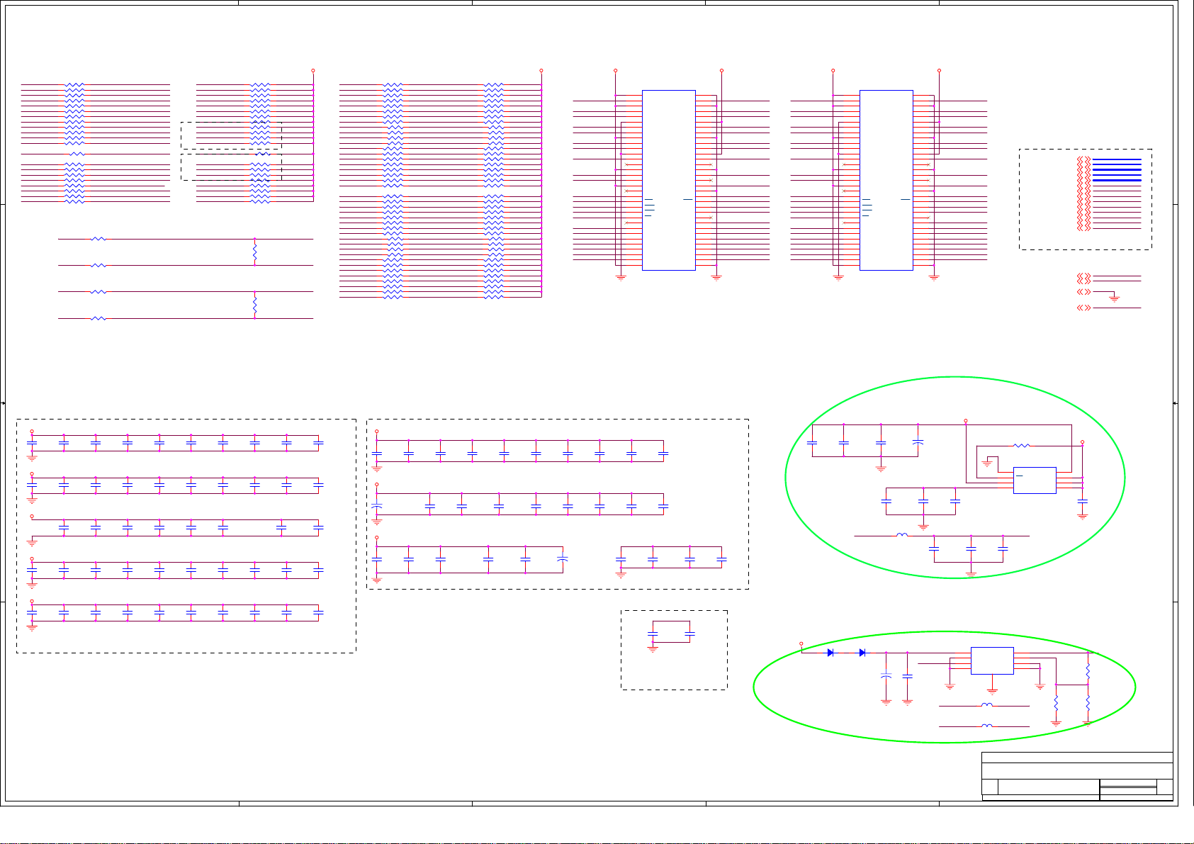
5
16/140
4
3
2
1
DV13_DDRDV13_DDR
RN0603/SMD
RN0603/SMD
R0603/SMD
R0603/SMD
R0603/SMD
R0603/SMD
RN0603/SMD
RN0603/SMD
RN0603/SMD
RN0603/SMD
R0603/SMD
R0603/SMD
R0603/SMD
R0603/SMD
RN0603/SMD
RN0603/SMD
MEM_DQ0
MEM_DQ1
MEM_DQ2
MEM_DQ3
MEM_DQ4
MEM_DQ5
MEM_DQ6
MEM_DQ7
MEM_DQS0
MEM_DQM0
MEM_DQM1
MEM_DQS1
MEM_DQ8
MEM_DQ9
MEM_DQ10
MEM_DQ11
MEM_DQ12
MEM_DQ13
MEM_DQ14
MEM_DQ15
MEM_DQ16
MEM_DQ17
MEM_DQ18
MEM_DQ19
MEM_DQ20
MEM_DQ21
MEM_DQ22
MEM_DQ23
MEM_DQS2
MEM_DQM2
MEM_DQM3
MEM_DQS3
MEM_DQ24
MEM_DQ25
MEM_DQ26
MEM_DQ27
MEM_DQ28
MEM_DQ29
MEM_DQ30
MEM_DQ31
RN8 75 x4
7 8
5 6
3 4
1 2
RN12 75x4
7 8
5 6
3 4
1 2
R122 75
R124 75
R126 75
R128 75
RN16 75x4
7 8
5 6
3 4
1 2
RN20 75x4
7 8
5 6
3 4
1 2
RN24 75x4
7 8
5 6
3 4
1 2
RN26 75x4
7 8
5 6
3 4
1 2
R133 75
R135 75
R138 75
R140 75
RN28 75x4
7 8
5 6
3 4
1 2
RN30 75x4
7 8
5 6
3 4
1 2
CLOSED TO DDRCLOSED TO MT5372
RN0603/SMD
RN0603/SMD
R0603/SMD
R0603/SMD
R0603/SMD
R0603/SMD
RN0603/SMD
RN0603/SMD
RN0603/SMD
RN0603/SMD
R0603/SMD
R0603/SMD
R0603/SMD
R0603/SMD
RN0603/SMD
RN0603/SMD
RDQ0
RDQ1
RDQ2
RDQ3
RDQ4
RDQ5
RDQ6
RDQ7
RDQS0
RDQM0
RDQM1
RDQS1
RDQ8
RDQ9
RDQ10
RDQ11
RDQ12
RDQ13
RDQ14
RDQ15
RDQ16
RDQ17
RDQ18
RDQ19
RDQ20
RDQ21
RDQ22
RDQ23
RDQS2
RDQM2
RDQM3
RDQS3
RDQ24
RDQ25
RDQ26
RDQ27
RDQ28
RDQ29
RDQ30
RDQ31
RN7 47 x4
7 8
5 6
3 4
1 2
RN11 47x4
7 8
5 6
3 4
1 2
R121 47
R123 47
R125 47
R127 47
RN15 47x4
7 8
5 6
3 4
1 2
RN19 47x4
7 8
5 6
3 4
1 2
RN23 47x4
7 8
5 6
3 4
1 2
RN25 47x4
7 8
5 6
3 4
1 2
R132 47
R134 47
R137 47
R139 47
RN27 47x4
7 8
5 6
3 4
1 2
RN29 47x4
7 8
5 6
3 4
1 2
RN0603/SMD
RN0603/SMD
RN0603/SMD
R0603/SMD
RN0603/SMD
RN0603/SMD
MEM_WE#
MEM_CAS#
MEM_RAS#
MEM_CS#
MEM_ADDR3
MEM_ADDR2
MEM_ADDR1
MEM_ADDR4
MEM_ADDR5
MEM_ADDR6
MEM_ADDR7
MEM_CLKEN
MEM_ADDR12
MEM_ADDR11
MEM_ADDR9RA9
MEM_BA0
MEM_BA1
MEM_ADDR10
23/12
23/12
MEM_WE#
MEM_CAS#
MEM_RAS#
MEM_CS#
MEM_ADDR10
MEM_BA1
MEM_BA0
MEM_ADDR13
MEM_ADDR7
MEM_ADDR6
MEM_ADDR5
MEM_ADDR4
MEM_CLKEN
MEM_ADDR8
MEM_ADDR9
MEM_ADDR11
MEM_ADDR12
MEM_ADDR0
MEM_ADDR1
MEM_ADDR2
MEM_ADDR3
RN6 75 x4
7 8
5 6
3 4
1 2
RN10 75x4
7 8
5 6
3 4
1 2
RN14 75x4
7 8
5 6
3 4
1 2
R130 NS/75
RN18 75x4
1 2
3 4
5 6
7 8
RN22 75x4
1 2
3 4
5 6
7 8
RN0603/SMD
RN0603/SMD
RN0603/SMD
R0603/SMD
RN0603/SMD
RN0603/SMD
RWE#
RN5 22 x4
7 8
RCAS#
5 6
RRAS#
3 4
RCS#
1 2
RA3
RN9 22 x4
D D
7 8
RA2
5 6
RA1
3 4
RA0 M EM_ADDR0
1 2
RA4
RN13 22x4
7 8
RA5
5 6
RA6
3 4
RA7
1 2
RCKE
R129 22
RA12
RN17 22x4
1 2
RA11
3 4
5 6
RA8 M EM_ADDR8
7 8
RA13 MEM_ADDR13
RN21 22x4
1 2
RBA0
3 4
RBA1
5 6
RA10
7 8
CLOSED TO MT5372 CLOSED TO DDR
RCLK0
R131
22
R0603/SMD
RCLK0#
R141
22
R0603/SMD
RCLK1
R142
22
C C
RCLK1#
R0603/SMD
R144
22
R0603/SMD
MEM_CLKA
R136
100
R0603/SMD
MEM_CLKA#
MEM_CLKB
R143
100
R0603/SMD
MEM_CLKB#
DV26_DDR DV 26_DDR DV26_DDR DV26_DDR
U16
1
MEM_DQ0
MEM_DQ1 MEM_DQ14
MEM_DQ2
MEM_DQ3
MEM_DQ4
MEM_DQ5
MEM_DQ6
MEM_DQ7
MEM_DQS0
MEM_ADDR13 MEM_ADDR13
MEM_DQM0
MEM_WE#
MEM_CAS#
MEM_RAS#
MEM_CS#
MEM_BA0
MEM_BA1
MEM_ADDR10
MEM_ADDR0
MEM_ADDR1
MEM_ADDR2
MEM_ADDR3
VDD
2
DQ0
3
VDDQ
4
DQ1
5
DQ2
6
VSSQ
7
DQ3
8
DQ4
9
VDDQ
10
DQ5
11
DQ6
12
VSSQ
13
DQ7
14
NC
15
VDDQ
16
LDQS
17
NC
18
VDD
19
NC
20
LDM
21
WE
22
CAS
23
RAS
24
CS
25
NC
26
BS0
27
BS1
28
A10/AP
29
A0
30
A1
31
A2
32
A3
VDD33VSS
16M x 16 DDR TSOP-66
TSOP_0D65_22D6LX9D7W_66SP
DDR#1
DQ15
VSSQ
DQ14
DQ13
VDDQ
DQ12
DQ11
VSSQ
DQ10
VDDQ
VSSQ
UDQS
VREF
UDM
66
VSS
DQ9
DQ8
NC
NC
VSS
CLK
CLK
CKE
NC
A12
A11
A9
A8
A7
A6
A5
A4
MEM_DQ15
65
64
63
MEM_DQ13
62
61
MEM_DQ12
60
MEM_DQ11
59
58
MEM_DQ10
57
MEM_DQ9
56
55
MEM_DQ8
54
53
52
MEM_DQS1
51
50
49
48
MEM_DQM1
47
MEM_CLKA#
46
MEM_CLKA
45
MEM_CLKEN
44
43
MEM_ADDR12
42
MEM_ADDR11
41
MEM_ADDR9
40
MEM_ADDR8
39
MEM_ADDR7
38
MEM_ADDR6
37
MEM_ADDR5
36
MEM_ADDR4
35
34
MEM_DQ16 MEM_DQ31
MEM_DQ17 MEM_DQ30
MEM_DQ18
MEM_DQ19
MEM_DQ20
MEM_DQ21
MEM_DQ22
MEM_DQ23
MEM_DQS2
MEM_DQM2
MEM_WE#
MEM_CAS#
MEM_RAS#
MEM_CS#
MEM_BA0
MEM_BA1
MEM_ADDR10
MEM_ADDR0
MEM_ADDR1
MEM_ADDR2
MEM_ADDR3
U17
1
VDD
2
DQ0
3
VDDQ
4
DQ1
5
DQ2
6
VSSQ
7
DQ3
8
DQ4
9
VDDQ
10
DQ5
11
DQ6
12
VSSQ
13
DQ7
14
NC
15
VDDQ
16
LDQS
17
NC
18
VDD
19
NC
20
LDM
21
WE
22
CAS
23
RAS
24
CS
25
NC
26
BS0
27
BS1
28
A10/AP
29
A0
30
A1
31
A2
32
A3
VDD33VSS
16M x 16 DDR TSOP-66
TSOP_0D65_22D6LX9D7W_66SP
DQ15
VSSQ
DQ14
DQ13
VDDQ
DQ12
DQ11
VSSQ
DQ10
VDDQ
VSSQ
UDQS
VREF
66
VSS
65
64
63
MEM_DQ29
62
61
MEM_DQ28
60
MEM_DQ27
59
58
MEM_DQ26
57
MEM_DQ25
56
DQ9
55
MEM_DQ24
54
DQ8
53
NC
52
MEM_DQS3
51
50
NC
VSS
UDM
CLK
CLK
CKE
NC
A12
A11
A9
A8
A7
A6
A5
A4
MEM_VREFMEM_VREF
49
48
MEM_DQM3
47
MEM_CLKB#
46
MEM_CLKB
45
MEM_CLKEN
44
43
MEM_ADDR12
42
MEM_ADDR11
41
MEM_ADDR9
40
MEM_ADDR8
39
MEM_ADDR7
38
MEM_ADDR6
37
MEM_ADDR5
36
MEM_ADDR4
35
34
RDQ[0..31]5
RDQS[0..3]5
RDQM[0..3]5
RA[0..13]5
RBA[0..1]5
RCLK05
RCLK0#5
RCS#5
RRAS#5
RCAS#5
RWE#5
RCKE5
RCLK15
RCLK1#5
RVREF5
DV26_DDR2,5,6
GND1,2,3,4,5,6,7,9,10,11,12,13,14
+5V1,2,7,9,11,13
DDR MEMORY
RDQ[0..31]
RDQS[0..3]
RDQM[0..3]
RA[0..13]
RBA[0..1]
RCLK0
RCLK0#
RCS#
RRAS#
RCAS#
RWE#
RCKE
RCLK1
RCLK1#
RVREF
DV26_DDR
+5V
CLOSED TO MT5372 CLOSED TO DDR
DV13_DDR
CB200
CB201
0.1uF
C0603/SMD
DV13_DDR
CB225
0.1uF
C0603/SMD
B B
DV13_DDR
DV13_DDR
CB263
0.1uF
C0603/SMD
DV13_DDR
CB275
0.1uF
C0603/SMD
A A
CB202
0.1uF
0.1uF
C0603/SMD
C0603/SMD
CB227
CB226
0.1uF
0.1uF
C0603/SMD
C0603/SMD
CB247
CB246
0.1uF
0.1uF
C0603/SMD
C0603/SMD
CB264
CB265
0.1uF
0.1uF
C0603/SMD
C0603/SMD
CB276
CB277
0.1uF
0.1uF
C0603/SMD
C0603/SMD
BYPASS CAP. FOR TERMINATOR
(EVERY 2 RESISTOR PUT 1 BYPASS CAP.)
CB203
0.1uF
C0603/SMD
CB228
0.1uF
C0603/SMD
CB248
0.1uF
C0603/SMD
CB266
0.1uF
C0603/SMD
CB278
0.1uF
C0603/SMD
CB204
0.1uF
C0603/SMD
CB229
0.1uF
C0603/SMD
CB249
0.1uF
C0603/SMD
CB267
0.1uF
C0603/SMD
CB279
0.1uF
C0603/SMD
CB205
0.1uF
C0603/SMD
CB230
0.1uF
C0603/SMD
CB250
0.1uF
C0603/SMD
CB268
0.1uF
C0603/SMD
CB280
0.1uF
C0603/SMD
CB206
0.1uF
C0603/SMD
CB231
0.1uF
C0603/SMD
CB251
0.1uF
C0603/SMD
CB269
0.1uF
C0603/SMD
CB281
0.1uF
C0603/SMD
CB207
0.1uF
C0603/SMD
CB232
0.1uF
C0603/SMD
CB270
0.1uF
C0603/SMD
CB282
0.1uF
C0603/SMD
CB208
0.1uF
C0603/SMD
CB233
0.1uF
C0603/SMD
CB252
0.1uF
C0603/SMD
CB271
0.1uF
C0603/SMD
CB283
0.1uF
C0603/SMD
CB209
0.1uF
C0603/SMD
CB234
0.1uF
C0603/SMD
CB253
0.1uF
C0603/SMD
CB272
0.1uF
C0603/SMD
CB284
0.1uF
C0603/SMD
DV26_DDR
CB215
0.1uF
C0603/SMD
DV26_DDR
+
CE43
220uF/16v
100UF/220UF/SMD
DV26_DDR
CB254
4.7uF/6.3V
C0603/SMD
CB216
0.1uF
C0603/SMD
CB255
4.7uF/6.3V
C0603/SMD
CB217
0.1uF
C0603/SMD
CB238
0.1uF
C0603/SMD
CB256
0.1uF
C0603/SMD
CB218
0.1uF
C0603/SMD
CB239
0.1uF
C0603/SMD
CB240
0.1uF
C0603/SMD
CB257
4.7uF/6.3V
C0603/SMD
CB219
0.1uF
C0603/SMD
CB220
0.1uF
C0603/SMD
CB241
0.1uF
C0603/SMD
CB258
4.7uF/6.3V
C0603/SMD
CB221
0.1uF
C0603/SMD
CB242
0.1uF
C0603/SMD
+
CE44
220uF/16V
100UF/220UF/SMD
CB222
CB223
0.1uF
0.1uF
C0603/SMD
C0603/SMD
CB244
CB243
0.1uF
0.1uF
C0603/SMD
C0603/SMD
MEM_VREF
CB259
0.1uF
C0603/SMD
PUT ON NEARLY BGA
CB224
4.7uF/6.3V
C0603/SMD
CB245
0.1uF
C0603/SMD
CB260
4.7uF/6.3V
C0603/SMD
RVREF
CB273
0.1uF
C0603/SMD
CB261
0.1uF
C0603/SMD
CB274
0.1uF
C0603/SMD
CB262
4.7uF/6.3V
C0603/SMD
CB197
4.7uF/6.3V
C0603/SMD
MEM_VREF
D49
DIODE SMD/NC
ZD/DIP/P10.0
CE65
220uF/16V/NC
CB198
4.7uF/6.3V
C0603/SMD
CB210
4.7uF/6.3V
C0603/SMD
L53
FB/70R/500mA/0603
BEAD/SMD/0603
+
CB199
0.1uF
C0603/SMD
BYPASS CAP. FOR DIMM
DV13_DDR FOR DDR TERMINATOR
MEM_VREF FOR DDR VREF
RVREF FOR MT5372 VREF
+5V
D48
DIODE SMD/NC
ZD/DIP/P10.0
100UF/220UF/SMD
CB437
4.7uF/6.3V/NC
C0603/SMD
RA-V3
5
4
3
2
DV13_DDR
+
CE42
220uF/16V
100UF/220UF/SMD
MEM_VREF
CB211
4.7uF/6.3V
C0603/SMD
CB235
4.7uF/6.3V
C0603/SMD
DV13_DDR
DV13_DDR RVREF
DV26_DDR
8
VTT
7
PVIN
6
AVIN
5
CB213
4.7uF/6.3V
C0603/SMD
CB212
0.1uF
C0603/SMD
U26
1
GND
2
SD
3
VSENSE
VREF4VDDQ
IC LP2996 DDR Termination SOP-8
SOP8/SMD
RVREF
CB237
CB236
0.1uF
4.7uF/6.3V
C0603/SMD
C0603/SMD
R145
4.7K
R0603/SMD
RA-V3
U27
1
VIN
VDDQ
2
NC
ADJSD
3
VTT
NC4GND
GND
CM3202/NC
9
CM3202-1
L51
FB/70R/500mA/0603/NC
BEAD/SMD/0603
L52
FB/70R/500mA/0603/NC
BEAD/SMD/0603
ZhongShan KAWA Electronic Inc.
Title
Size
Custom
Date: Sheet
DV26_DDR
8
7
6
GND
5
MEM_VREFDV13_DDR
DDR1 MEMORY
Document Number
MT5371_V07
R403
120K/NC
R0603/SMD
1
R146
10K/NC
R0603/SMD
R402
10K/NC
R0603/SMD
Drawn:
Checked:
<Designer>
<Checker>
814Thursday, March 01, 2007
Rev
1
of
Page 19
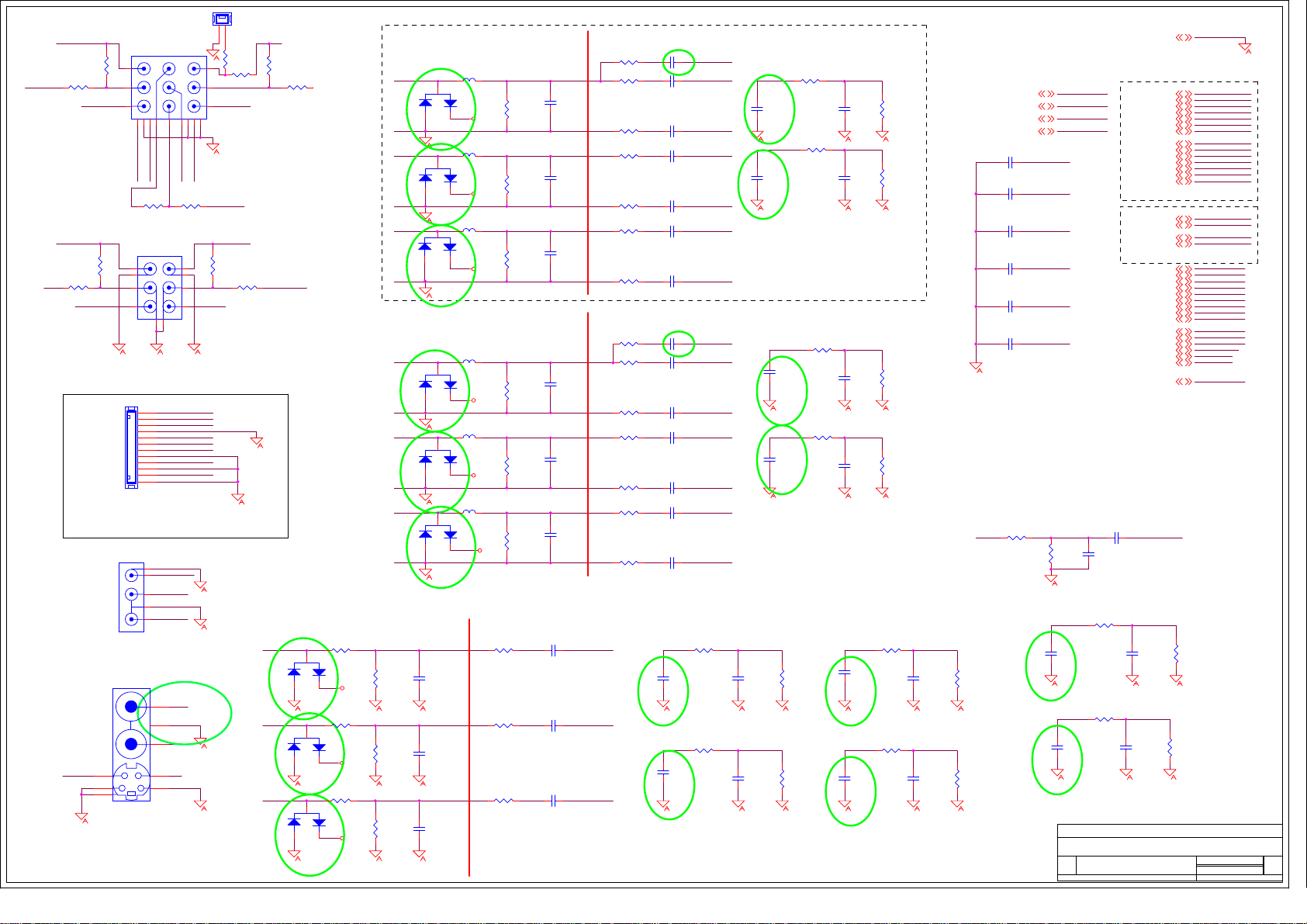
R147
17/140
68
R0603/SMD
R148
68
R0603/SMD
R152
100
R0603/SMD
R155
68
R0603/SMD
R160
100
R0603/SMD
R161
68
R0603/SMD
R163
100
R0603/SMD
R168
68
R0603/SMD
R170
68
R0603/SMD
R173
100
R0603/SMD
R174
68
R0603/SMD
R178
100
R0603/SMD
R179
68
R0603/SMD
R181
100
R0603/SMD
RA-V1
RA-V1
A
R187
47K
R0603/SMD
R194
47K
R0603/SMD
AGND_AFE
SOY0
Y0P
Y0N
PB0P
PB0N
PR0P
PR0N
SOY1
Y1P
Y1N
PB1P
PB1N
PR1P
PR1N
YPBPR0R_IN1
YPBPR0L_IN1
YPBPR1R_IN1
YPBPR1L_IN1
SC0
SY0
CVBS1
SC1
SY2
CVBS3
SC2
SY1
CVBS2
DVD_IR
VGAR_IN1
VGAL_IN1
ASPDIFASPDIF
AUD_LOUT
AUD_ROUT
+5V
Drawn:
Checked:
<Designer>
<Checker>
914Thursday, Ma rch 01, 2007
Rev
2
of
AGND_AFE1,2,3,4,5,6,7,8,10,11,12,13,14
SOY0
CB286
1nF
C0603/SMD
Y0P
CB287
10nF
C0603/SMD
Y0N
CB293
10nF
C0603/SMD
PB0P
CB294
10nF
C0603/SMD
PB0N
CB300
10nF
C0603/SMD
PR0P
CB301
10nF
C0603/SMD
PR0N
CB304
10nF
C0603/SMD
SOY1
CB306
1nF
C0603/SMD
Y1P
CB308
10nF
C0603/SMD
Y1N
CB312
10nF
C0603/SMD
PB1P
CB313
10nF
C0603/SMD
PB1N
CB317
10nF
C0603/SMD
PR1P
CB318
10nF
C0603/SMD
PR1N
CB320
10nF
C0603/SMD
R185
AVR_IN
1.5K
R0603/SMD
CB326
NC
C0603/SMD
R196
1.5K
R0603/SMD
CB333
NC
C0603/SMD
A
RA-V1
RA-V1
CB327
220P
C0603/SMD
CB334
220P
C0603/SMD
YPBPR0R_IN
CB290
NC
C0603/SMD
YPBPR0L_IN
CB297
NC
C0603/SMD
YPBPR1R_IN
CB309
NC
C0603/SMD
AGND_AFE
YPBPR1L_IN
CB315
NC
C0603/SMD
RA-V1
RA-V1
R189
47K
R0603/SMD
R198
47K
R0603/SMD
R149
1.5K
R0603/SMD
R154
1.5K
R0603/SMD
R169
1.5K
R0603/SMD
AGND_AFE
R175
1.5K
R0603/SMD
RA-V1
RA-V1
YPBPR0R_IN1
CB291
220P
C0603/SMD
YPBPR0L_IN1
CB298
220P
C0603/SMD
YPBPR1R_IN1
CB310
220P
C0603/SMD
YPBPR1L_IN1
CB316
220P
C0603/SMD
AVL_IN
CB324
NC
C0603/SMD
SYL_INSYR_IN
CB335
NC
C0603/SMD
R151
47K
R0603/SMD
R157
47K
R0603/SMD
R171
47K
R0603/SMD
AGND_AFE
R177
47K
R0603/SMD
R186
1.5K
R0603/SMD
R197
1.5K
R0603/SMD
AVL_IN1AVR_IN1
CB328
220P
C0603/SMD
SYL_IN1SYR_IN1
CB336
220P
C0603/SMD
SYL_IN111
SYR_IN111
AVL_IN111
AVR_IN111
CB285
47nF
C0603/SMD
CB288
47nF
C0603/SMD
CB292
47nF
C0603/SMD
CB295
47nF
C0603/SMD
CB299
47nF
C0603/SMD
CB302
47nF
C0603/SMD
ASPDIFASPDIF COAXIAL_OUT
R190
47K
R0603/SMD
R199
47K
R0603/SMD
SYL_IN1
SYR_IN1
AVL_IN1
AVR_IN1
CVBS2
SY1
SC1
CVBS3
SY2
SC2
R165
100
R0603/SMD
R167
100
R0603/SMD
VGAR_INVG AR_INVGAR_IN
RA-V1
CB322
NC
C0603/SMD
VGAL_IN VGAL_IN1
RA-V1
CB330
NC
C0603/SMD
ZhongShan KAWA Electronic Inc.
Title
Document Number
Size
Custom
Date: Sheet
SOY05
Y0P5
Y0N5
PB0P5
PB0N5
PR0P5
PR0N5
SOY15
Y1P5
Y1N5
PB1P5
PB1N5
PR1P5
PR1N5
YPBPR VIDEO INPUT
YPBPR0R_IN111
YPBPR0L_IN111
YPBPR1R_IN111
YPBPR1L_IN111
YPBPR AUDIO INPUT
CB305
0.1uF
C0603/SMD
CB307
330pF
C0603/SMD
R182
1.5K
R0603/SMD
R191
1.5K
R0603/SMD
YPBPR INPUT
MT5371_V07
SC05
SY05
CVBS15
SC15
SY25
CVBS35
SC25
SY15
CVBS25
DVD_IR7
VGAR_IN111
VGAL_IN111
ASPDIF5
AUD_LOUT11
AUD_ROUT11
+5V1,2,7,8,11,13
VGAR_IN1
CB323
220pF
C0603/SMD
CB331
220pF
C0603/SMD
J12
DIP2/W/H/P2.54
2x1 W/HOUSING
1
9
11
Y_GND
PB0_IN
R391
0R
R0603/SMD
4
3
2
AGND_AFE
SYL_IN
2
15
13
12
14
AGND_AFE
PB1_IN
R0603/SMD
YPBPR0R_IN
AGND_AFE
R93
0.1uf
0603/SMD
R0603/SMD
Y0_IN
VGAR_INVGAL_IN
R166
0R/NC
R0603/SMD
R393
0R
R92
0R
RA-V1
RA-V1
AV1_IN
R153
0R/NC
R0603/SMD
R395
0R
R0603/SMD
YPBPR1R_IN
NEARLY YPBPR CONNECTOR NEARLY MT5372
Y0_IN
D8
BAV99
SOT23/SMD
Y_GND
PB0_IN
D9
BAV99
SOT23/SMD
PB_GND
PR0_IN
D10
BAV99
SOT23/SMD
PR_GND
RA-V1
2
1
2
1
2
1
L54
FB/70R/500mA/0603
BEAD/SMD/0603
3
+5V
L55
FB/70R/500mA/0603
BEAD/SMD/0603
3
+5V
RA-V1
L56
FB/70R/500mA/0603
BEAD/SMD/0603
3
+5V
RA-V1
NEARLY YPBPR CONNECTOR NEARLY MT5372
D11
BAV99
SOT23/SMD
D12
BAV99
SOT23/SMD
D13
BAV99
SOT23/SMD
RA-V1
Y1_IN
Y_GNDY_GND
PB1_IN
PB_GNDPB_GND
PR1_IN
PR_GNDPR_GND
2
1
2
1
2
1
L57
FB/70R/500mA/0603
BEAD/SMD/0603
3
+5V
L58
FB/70R/500mA/0603
BEAD/SMD/0603
3
+5V
RA-V1
L59
FB/70R/500mA/0603
BEAD/SMD/0603
3
+5V
RA-V1
NEARLY YPBPR CONNECTOR
NEARLY AV CONNECTOR NEARLY MT5372
AV1_IN
D14
BAV99
SOT23/SMD
SY0_IN
D15
BAV99
SOT23/SMD
SC0_IN
D16
BAV99
SOT23/SMD
R183
0
2
R0603/SMD
1
3
+5V
R192
0
2
R0603/SMD
1
3
+5V
R200
0
2
R0603/SMD
1
3
+5V
R188
75
R0603/SMD
R195
75
R0603/SMD
R202
75
R0603/SMD
CB325
47pF
C0603/SMD
CB332
47pF
C0603/SMD
CB338
47pF
C0603/SMD
R150
75
R0603/SMD
R158
75
R0603/SMD
R162
75
R0603/SMD
R172
75
R0603/SMD
R176
75
R0603/SMD
R180
75
R0603/SMD
R184
100
R0603/SMD
R193
100
R0603/SMD
R201
100
R0603/SMD
CB289
15pF
C0603/SMD
CB296
15pF
C0603/SMD
CB303
15pF
C0603/SMD
CB311
15pF
C0603/SMD
CB314
15pF
C0603/SMD
CB319
15pF
C0603/SMD
CB321
47nF
C0603/SMD
CB329
47nF
C0603/SMD
CB337
47nF
C0603/SMD
CVBS1
SY0
SC0
AVR_IN
R159
0R/NC
R0603/SMD
R394
PR1_IN Y1_IN
0R
R0603/SMD
PR0_IN
R164
0R/NC
R0603/SMD
R392
YPBPR1L_IN
0R
R0603/SMD
YPBPR0L_IN
AGND_AFE
A A
RCA3X3
AV9-8.4-13BA
3
2
1
45678
PR_GND
PB_GND
R156
0R/NC
R0603/SMD
P3
RCA3X2
AV6-8.4-13B
10
9
8
7
J4
1
2
3
4
5
6
7
R. ANGLE
8
9
10
11
12
12P2.0mm/NC
DIP12/W/H/P2.0
P1
10
AVL_IN
156
AGND_AFE
PR1_IN
PR_GND
Y1_IN
PB1_IN
PB_GND
DVD_IR
YPBPR1L_IN
YPBPR1R_IN
YPBPR 2 INPUT.
1
COAXIAL_OUT
2
AUD_LOUT
3
4
AUD_ROUT
5
av3-8.3-09P
RCA3X2
P2
AV-S-3
RA-V3
6
8
SYR_IN
7
SC0_IN
43
CY
21
GG
P4
SY0_IN
5
S-VIDEO FIRST + RCA
RA-V1
Page 20
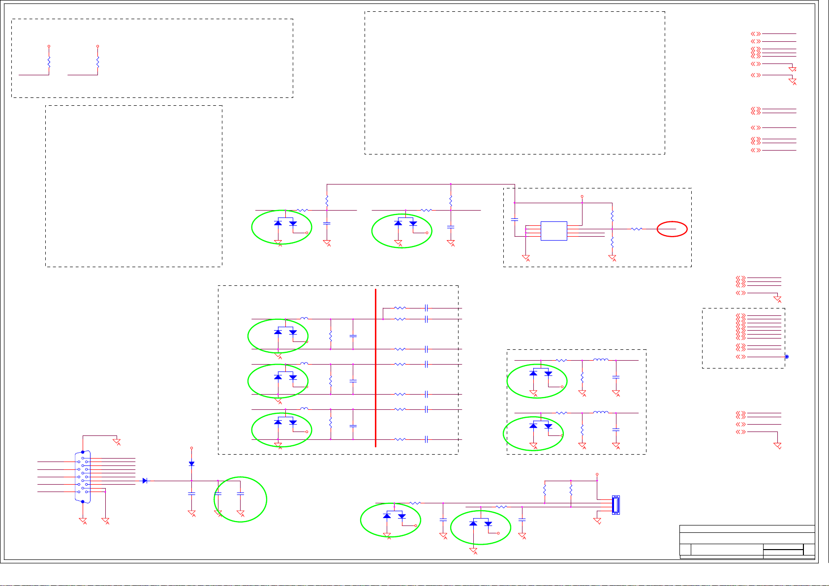
A
18/140
DEL: D17~D27_D60_P5_U20_Q10_Q19_CB340
DEL: R36_RR82_R83_R208_R209_R210_R211_R212_R216_R217_R218_R390_R408
VGASDA_INVGASDA_IN
D29
BAV99
SOT23/SMD
R221
20K
R0603/SMD
R223
100
2
R0603/SMD
1
3
VGASDAVGASDAVGASCLVGASCL
CB343
NC/47PF
C0603/SMD
CB341
0.1uF
C0603/SMD
VGA_PLUGPWR
U22
1
2
3
EEPROM 24C04
SOP8/SMD
NC
NC
NC
GND4SDA
VCC
WP
SCL
VGA_PLUGPWR
8
VGAROMWP
7
VGASCL
6
VGASDA
5
R224
20K
R0603/SMD
R228
10K/NC
R0603/SMD
2006.12.16
H : WP ENABLE
L : WP DISABLE
R227
33
R0603/SMD
GPIO_8
RA-V3
DV331,2,4,5,6,7,11,12,13,14
+5V1,2,7,8,9,11,13
DV33SB1,2 ,5,6,7,11,12,13
AV332,6,11
AV152,6
AGND_HDMI1,2,3,4,5,6,7,8,9,11,12,13,14
AGND_AFE1,2,3,4,5,6,7,8,9,11,12,13,14
OSDA25
OSCL25
SIF INTERFACE
OWRP2
GPIO_85,14
GPIO_25,14
GPIO_165,7,13
DV33
+5V
DV33SB
AV33
AV15
AGND_HDMI
AGND_AFE
OSDA2
OSCL2
OWRP2
GPIO_8
GPIO_2
GPIO_16
OSCL2
PULL HIGH AV33
AV33 AV33
R204
10K
R0603/SMD
OSDA2
R205
10K
R0603/SMD
DEL: R214_R2 1 9 _ R 2 1 5 _R213_U21_R225_R226
DEL; CB339_R203_R206_R207_U19
HDMI HDCP EEPROM
2006.12.16
R220
20K
VGASCL_INVGASCL_IN
2
D28
BAV99
RA-V1 RA-V1
SOT23/SMD
1
3
VGA_PLUGPWR VGA_PLUGPWR
R222
100
R0603/SMD
R0603/SMD
CB342
NC/47PF
C0603/SMD
2006.12.16
+5VSB1,2,7,11,12,13,14
A A
NEARLY VGA CONNECTOR NEARLY MT5372
CB344
1nF
C0603/SMD
CB345
10nF
C0603/SMD
CB347
10nF
C0603/SMD
CB348
10nF
C0603/SMD
CB351
10nF
C0603/SMD
CB352
10nF
C0603/SMD
CB355
10nF
C0603/SMD
U0RX
SOG
GP
GN
BP
BN
RP
RN
CB359
22pF
C0603/SMD
D38
BAV99
SOT23/SMD
R244
4.7K
R0603/SMD
L61
2.2uH
BEAD/SMD/0603
R235
2K
R0603/SMD
L64
2.2uH
BEAD/SMD/0603
R241
2K
R0603/SMD
DV33SB
CB349
5pF
C0603/SMD
CB354
5pF
C0603/SMD
J8
1
2
3
4
4P2.0mm
DIP4/W/H/P2.0
VSYNC
HSYNC# HSYNC
D31
BAV99
SOT23/SMD
RA-V1
VSYNC#
D34
BAV99
SOT23/SMD
RA-V1
3
R246
0
R0603/SMD
+5VSB
U0TXTXDTXD
CB360
22pF
C0603/SMD
TXDTXDTXDTXDTXDTXD
2
1
R233
510
2
R0603/SMD
1
3
VGA_PLUGPWR
R239
510
2
R0603/SMD
1
3
VGA_PLUGPWR
R243
4.7K
R0603/SMD
FOR CODE DOWN LOAD AND DEBUGGING
RA-V1
RXDRXDRXDRXD
VGASDA_IN
HSYNC#
VSYNC#
VGASCL_IN
D-SUB15 FEMALE
DSUB15/DIP/F
R229
68
2
1
2
1
2
1
L60
FB/70R/500mA/0603
BEAD/SMD/0603
3
VGA_PLUGPWR
L62
FB/70R/500mA/0603
BEAD/SMD/0603
3
VGA_PLUGPWR
L63
FB/70R/500mA/0603
BEAD/SMD/0603
3
VGA_PLUGPWR
R231
75
R0603/SMD
R236
75
R0603/SMD
R240
75
R0603/SMD
RA-V1
CB346
5pF
C0603/SMD
CB350
5pF
C0603/SMD
CB353
5pF
C0603/SMD
SOT23/SMD
D37
BAV99
GRN
D30
BAV99
RA-V1
SOT23/SMD
GRN_GNDGRN _GND
BLU
D32
BAV99
SOT23/SMD
RA-V1
BLU_GNDBLU_GND
RED
D33
BAV99
RA-V1
SOT23/SMD
CB358
1uF/16v
C0603/SMD
RED_GNDRED_GND
RA-V1
1617
RED_GND
6
RED
1
11
12
13
14
15
P6
GRN_GND
7
GRN
2
BLU_GND
8
BLU
3
9
TXD
4
10
5
D36
VGA_PLUGPWRVGA_PLUGPWR
1N4148
1N4148/SMD
+5VSB
D35
1N4148
1N4148/SMD
CB356
1uF/16v
C0603/SMD
CB357
1uF/16v
C0603/SMD
R0603/SMD
R230
68
R0603/SMD
R232
100
R0603/SMD
R234
68
R0603/SMD
R237
100
R0603/SMD
R238
68
R0603/SMD
R242
100
R0603/SMD
R245
0
RXD
R0603/SMD
2
1
3
+5VSB
A
DV33SB1,2,5,6,7,11,12,13
AV332,6,11
AGND_AFE1,2,3,4,5,6,7,8,9,11,12,13,14
SOG5
GP5
GN5
BP5
BN5
RP5
RN5
HSYNC5
VSYNC5
FB_IN5
VGA VIDEO INPUT
U0TX5
U0RX5
GPIO_15,7
AGND_PLL1,2,3 , 4,5,6,7,8,9,11,12,13,14
ZhongShan KAWA Electronic Inc.
Title
HDMI /VGA INPUT
Document Number
Size
Custom
MT5371_V07
Date: Sheet
+5VSB
DV33SB
AV33
AGND_AFE
SOG
GP
GN
BP
BN
RP
RN
HSYNC
VSYNC
FB_IN
U0TX
U0RX
GPIO_1
AGND_PLL
Drawn:
Checked:
TP50
<Designer>
<Checker>
10 14Thursday, March 01, 2007
Rev
1
of
Page 21
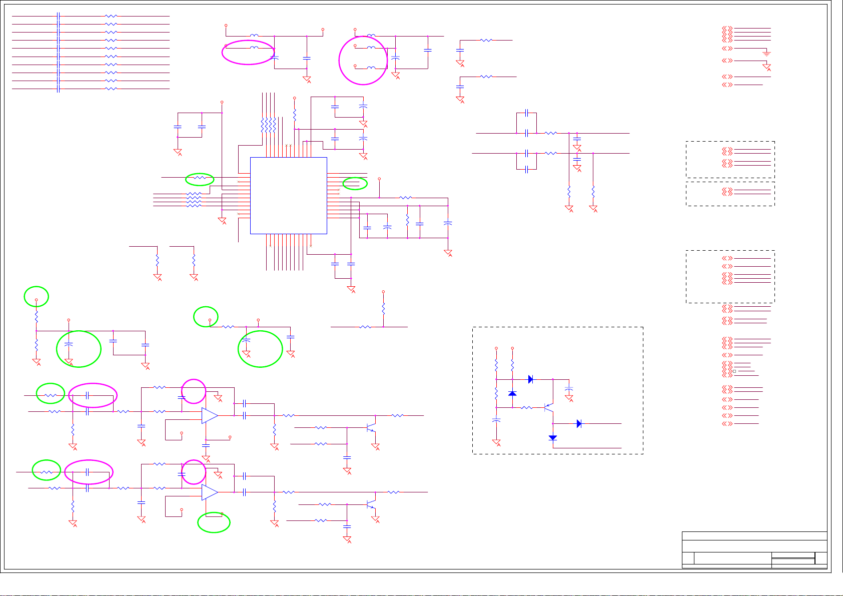
CE46
19/140
+
100uF/16V
100UF/220UF/SMD
R264 R266 Only For
CE2816
R264 1K/NC
R0603/SMD
R266
CE50
+
1K/NC
47uF/16V
100UF/220UF/SMD
R0603/SMD
R272
1K
R0603/SMD
R282
AUD_LOUT
100
R0603/SMD
R292
AUD_ROUT
100
R0603/SMD
A
+9V1,2
+12V1,13
+5V1,2,7,8,9,13
DV331,2,4,5,6,7,12,13,14
GND1,2,3,4,5,6,7,8,9,10,12,13,14
AGND_AFE1,2,3,4,5,6,7,8,9,10,12,13,14
+5V_TUNER2,3
AO1SDATA35
YPBPR0R_IN19
YPBPR0L_IN19
YPBPR1R_IN19
YPBPR1L_IN19
YPBPR AUDIO INPUT
VGAR_IN19
VGAL_IN19
VGA AUDIO INPUT
I2SIN_DATA5
AO1SDATA45
AO1MCLK5
AO1BCK5
AO1LRCK5
VCCWM
CB385
0.1uF
5V_A
CB368
0.1uF
SCL14
CB374
47pF
C0603/SMD
CB373
47pF
C0603/SMD
+
CE49
47uF/16V
100UF/220UF/SMD
R258
0
SIF_SCL
R0603/SMD
R257
0
SIF_SDASDA14
R0603/SMD
CB375
4.7uF/6.3V
C0603/SMD
CB378
R260
AVOUT_R AO1AUXRAO1AUXR
AVOUT_L
4.7uF/6.3V
C0603/SMD
CB384
4.7uF/6.3V
C0603/SMD
0
R0603/SMD
CB382
R261
4.7uF/6.3VC0603/SMD
0
R0603/SMD
R262
47K
R0603/SMD
CB380
100pF
C0603/SMD
CB383
100pF
C0603/SMD
AO1AUXL
R263
47K
R0603/SMD
AO1AUXR
AUDIO I2S INTERFACE
AO1AUXR12
AO1AUXL12
ON/OFF_MUTE112
GPIO_195
SIF_SDA4,7
SIF_SCL4,7
AUD_LOUT9
AUD_ROUT9
AVL_IN19
AVR_IN19
SYL_IN19
SYR_IN19
AL15
AR15
DV33SB1,2,5,6,7,10,12,13
+5VSB1,2,7,10,12,13,14
+9V1,2
AV332,6,10
ZhongShan KAWA Electronic Inc.
Title
AUDIO CODEC
Document Number
Size
Custom
MT5371_V07
Date: Sheet
R274
R273
0
NC
D39 1N4148
1 2
D40
1N4148
1 2
R277 470
CE54
100uF/16V
100UF/220UF/SMD
MUTE CIRCUIT
32
Q11
1
2N3906
12
D42
1N4148
CE53
470uF/16V
+
D41 1N4148
1 2
ON/OFF_MUTE1
ON/OFF_MUTE2
+5V +9V
R276
22k
*
+
A
+9V
+12V
+5V
DV33
GND
AGND_AFE
+5V_TUNER
AO1SDATA3
YPBPR0R_IN1
YPBPR0L_IN1
YPBPR1R_IN1
YPBPR1L_IN1
VGAR_IN1
VGAL_IN1
I2SIN_DATA
AO1SDATA4
AO1MCLK
AO1BCK
AO1LRCK
AO1AUXR
AO1AUXL
ON/OFF_MUTE1
GPIO_19
SIF_SDA
SIF_SCL
AUD_LOUT
AUD_ROUT
AVL_IN1
AVR_IN1
SYL_IN1
SYR_IN1
AL1
AR1
DV33SB
+5VSB
+9V
AV33
Drawn:
Checked:
<Designer>
<Checker>
11 14Thu r s da y, M arc h 01, 2007
Rev
2
of
CB361
+9V
R268
47K
R0603/SMD
R271
47K
R0603/SMD
29/01/2007
R83
0
R0603/SMD
AL1
R0603/SMD
R82
0
R0603/SMD
AR1
4.7uF/6.3V C0603/SMD
CB362
4.7uF/6.3V C0603/SMD
CB363
3.3uF/10V C0603/SMD
CB364
4.7uF/6.3V C0603/SMD
CB365
4.7uF/6.3V C0603/SMD
CB366
4.7uF/6.3V C0603/SMD
CB369
4.7uF/6.3V C0603/SMD
CB370
4.7uF/6.3V C0603/SMD
CB371
4.7uF/6.3V C0603/SMD
CB372
4.7uF/6.3V C0603/SMD
OPAVREF OP9V
+
CE52
100uF/16V
100UF/220UF/SMD
RA-V1
R278
0
R283
10K/NC
R0603/SMD
21/12/2006 21/12 /2006
R288
0
R0603/SMD
R293
10K/NC
R0603/SMD
VGAR_IN1
VGAL_IN1
YPBPR0R_IN1
YPBPR0L_IN1
YPBPR1R_IN1
YPBPR1L_IN1
SYR_IN1 SYR
AVL_IN1
RA-V3
A A
AL3
29/01/2007
AR3
R247
20K
R248
20K
R249
20K
R250
20K
R251
20K
R252
20K
R253
20K
R254
20K
R255
20K
R256
20K
R0603/SMD
R0603/SMD
R0603/SMD
R0603/SMD
R0603/SMD
R0603/SMD
R0603/SMD
R0603/SMD
R0603/SMD
R0603/SMD
I2SIN_DATA
VGAR
VGAL
YPBPR0R
YPBPR0L
YPBPR1R
YPBPR1L
SYLSYL_I N1
AVRAVR_IN1
AVL
I2SIN_DATA
AO1LRCK
AO1BCK
AO1MCLK
AO1SDATA3
R265
10K/NC
R0603/SMD
CB376
0.1uF
C0603/SMD
R0603/SMD
RN0603/SMD
AO1LRCK
DVDD
29/01/2007
R36
RN32
33x4
R267
10K/NC
R0603/SMD
CB377
4.7uF/6.3V
C0603/SMD
0
12
34
56
78
RA-V3
+9V
R279
10K
R0603/SMD
R289
10K
R0603/SMD
CB391
0.1uF
CB396
820pF
C0603/SMD
CB403
820pF
C0603/SMD
R275
20K
R0603/SMD
R280
5.1K
R0603/SMD
R287
20K
R0603/SMD
R290
5.1K
R0603/SMD
CB392
100pF
C0603/SMD
OPAVREF
CB399
100pF
C0603/SMD
OPAVREF
-
2
+
3
8 4
-
6
+
5
8 4
CB390
4.7uF/6.3V
C0603/SMD
21/12/2006 21/12/2006
CB465
4.7uF/6.3V
C0603/SMD
CB394
4.7uF/6.3V
C0603/SMD
CB466
4.7uF/6.3V
C0603/SMD
CB401
4.7uF/6.3V
C0603/SMD
RA-V1
DV33SB
L65 FB /NC
DV33SB
DV33 +5V
L73
FB/70R/50 0 mA / 0603
BEAD/SMD/0603
+
CE45
47uF/16V
100UF/220UF/SMD
DVDD
DVDD
CB367
0.1uF
AUDIO CODEC
DVDD
RA-V1
U24A
1
BA4558 OPA
SOP8/SMD
CB397
0.1uF
C0603/SMD
U24B
7
BA4558 OPA
SOP8/SMD
OP9V
RN31
U23
1
DIN1
2
DIN2
3
DIN3
4
DOUT
5
DVDD
6
DGND
7
LRCK_AD
8
BCLK_AD
9
MCLK_AD
10
DGND
11
NC
12
AIN5R
VGAR
I2S UP TO 24-BIT DATA
R269
10R/0805
R0805/SMD
CE51
+
220uF/16V
100UF/220UF/SMD
CB393
4.7uF/6.3V
C0603/SMD
CB395
4.7uF/6.3V
C0603/SMD
OP9V
CB400
4.7uF/6.3V
C0603/SMD
CB402
4.7uF/6.3V
C0603/SMD
5V_A
AO1BCK
AO1MCLK
AO1LRCK
AO1SDATA4
33x4
SDA14
SCL14
1 2
3 4
5 6
7 8
44
43
46
41
45
47
48
NC42NC
SCL
SDA
BCLK_DA
LRCK_DA
MCLK_DA
AIN5L13NC14AIN4R15AIN4L16AIN3R17AIN3L18AIN2R19AIN2L20AIN1R21AIN1L22AVDDAD23NC
SYL
SYR
VGAL
YPBPR0R
YPBPR0L
YPBPR1L
YPBPR1R
CB389
0.1uF
C0603/SMD
R281
100
R0603/SMD
ON/OFF_MUTE2
R284
10K/NC
R0603/SMD
OUT_MUTE
R291
100
R0603/SMD
R294
10K/NC
R0603/SMD
OUT_MUTE
R259
180R
RN0603/SMD
39
37
DAVMC
VOUT1R
DACREFP40DACREFP
DACREFN38DACREFN
VOUT1L
VOUT2R
VOUT2L
VOUT3R
VOUT3L
AVDD_DA
AGND_DA
ADCVMID
ADCVREFN
ADCVREFP
AGNDAD
24
AVL
AVR
C0603/SMD
2X GAIN
2X GAIN
ON/OFF_MUTE2
CE2816/CE2836
CB387
0.1uF
R285
2K
R0603/SMD
R286
2K
R0603/SMD
R296
2K
R0603/SMD
+5VSB
L66
FB/NC
L74
FB/NC
BEAD/SMD/0603
DV33
L72
FB/70R/50 0 mA / 0603
BEAD/SMD/0603
2006.12.18
CB381
+
CE48
0.1uF
47uF/16V
C0603/SMD
100UF/220UF/SMD
+
CE47
CB379
100uF/16V
0.1uF
AVOUT_R
AVOUT_L
AR3
AL3
29/01/2007
CB388
0.1uF
C0603/SMD
R270 0
CB398
NC
C0603/SMD
CB404
NC
C0603/SMD
100UF/220UF/SMD
5V_A
CB386
0.1uF
C0603/SMD
AV33
Q12
1
2N3904
SOT23/SMD
3 2
Q13
1
2N3904
SOT23/SMD
3 2
C0603/SMD
36
35
34
33
32
31
30
29
28
27
26
25
GPIO_19 OUT_MUTE
R295
2K
R0603/SMD
INTERNAL AUDIO DAC OUTPUT
Page 22
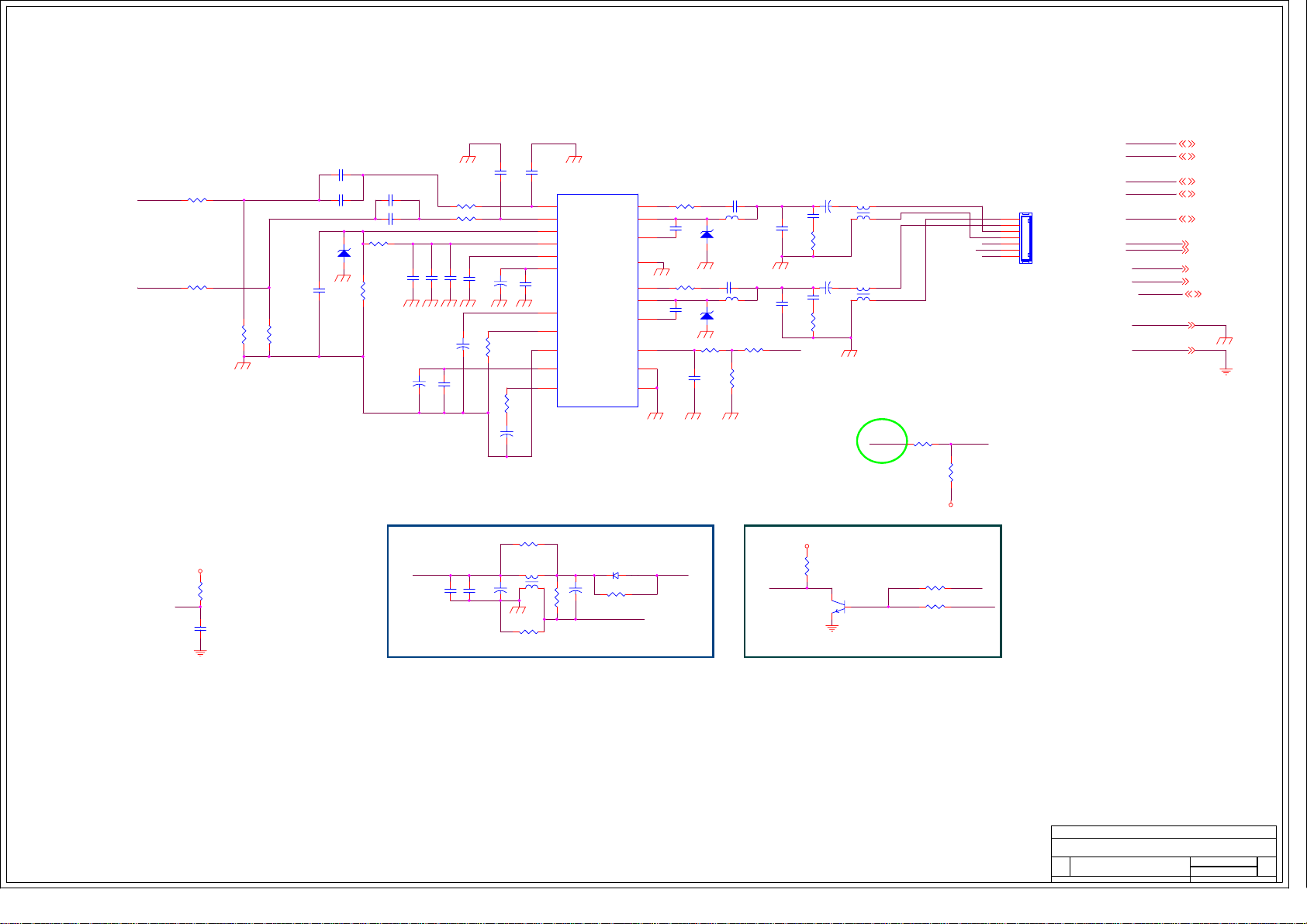
A
20/140
DV33
AGND_AFE1,2,3,4,5,6,7,8,9,10,11,13,14
AMP_GND
+5VSB
+24V
DV33SB
OPCTRL3
GPIO_10
AO1AUXL
AO1AUXR
ON/OFF_MUTE1
CB405
4.7uF/6.3V
C0603/SMD
R297
AO1AUXL
0
R0603/SMD
change 2/16
AO1AUXR
R303
0
R0603/SMD CB423
47K
R307
A A
DV33
R318
10K
R0603/SMD
GPIO_10
CB429
0.1uF
C0603/SMD
CB421
0.1uF
C0603/SMD
R308
47K
R0603/SMD
R0603/SMD
CB408
4.7uF/6.3V
C0603/SMD
D44
SMD 4.7V
R304
100K
R0603/SMD
D300
R/SMD/1206
R302
3.3K
CB409
4.7uF/6.3V
C0603/SMD
CB411
4.7uF/6.3V
C0603/SMD
CE59
10uF/35V
10UF/SMD
CB415
VD
R0603/SMD
1uF/50V
CB416
C1210/SMD
CE58
10uF/35v
10UF/SMD
+
CB427
0.1uF/50V
C0603/SMD
R298 10K
R0603/SMD
R300 10K
C0603/SMD
0.1uF/50V
C0603/SMD
CB417
0.1uF/50V
+
CB426
0.1uF/50V
CB428
0.1uF/50V
C0603/SMD
CB418
0.1uF/50V
10UF/SMD
C0603/SMD
1000uF/35v
CAP7X13\5
CE61
C0603/SMD
R309
33K
R0603/SMD
CB406
+
CE56
10uF/35v
R313
+
+
1500P
C0603/SMD
VD
VD
CB419
47nF
C0603/SMD
1K
R0603/SMD
CE60
3.3uF/50v
R316 NC
R1206/SMD
L71
#C3B-A0619
L04A/dip
4
312
R323
NC
R1206/SMD
CB407
33UF/47UF/SMD
1500P
C0603/SMD
5
11
3
2
14
18
6
7
8
9
10
R320
R2S15102NP
IN1
IN2
STBY
VD1
VD2
DVDD
CBIAS
ROSC
GND
AVDD
PROT
CE62
1000uF/35V/NC
CAP7X13\5
+
RCF/4
1K/NC 2W
U25
QFp20
MUTEL
D46
SR260/NC
ZD/DIP/P10.0
R321 0R/1206
R1206/SMD
AMP_GND
PWM1
OUT1
PWM2
OUT2
CB413
CB424
R310
R0603/SMD
CB425
0.1uF
C0603/SMD
CB410
3pF
C0603/SMD
L68
BEAD/15UH/DIP
L\DIP\P5.0\D10.5
D43
D300
DIODE SMD ZENER 33V
CB420
3pF
C0603/SMD
L70
BEAD/15UH/DIP
D45
L\DIP\P5.0\D10.5
D300
DIODE SMD ZENER 33V
R311
1K
47K
R0603/SMD
R312
150K
R0603/SMD
R299
150K
R0603/SMD
4
1
0.1uF/50V
19
HB1
C0603/SMD
21
GND
HB2
VS1
VS2
R305
150K
12
R0603/SMD
15
0.1uF/50V
17
C0603/SMD
13
20
16
+24V
CB414
0.33uF/63V
J2\5\7.5
MUTE_RES
R317
4.7K
R0603/SMD
0.33uF/63V
J2\5\7.5
+5VSB
Q14
2N3904
CE55
1000uF/35v
CAP7X16\5
+
CB412
474/50V/1210
C1210/SMD
R301
8.2R/0.5W /1210
2010/SMD
CE57
1000uF/35v
CAP7X16\5
+
CB422
474/50V/1210
C1210/SMD
R306
8.2R/0.5W /1210
2010/SMD
3 2
L67
LOUT
134
2
#C3H-A0028
L-A/5
ROUT
L69
143
2
#C3H-A0028
L-A/4
OPCTRL3 AMP_MUTE
RA-V3
1
R314 0
R0603/SMD
R0603/SMD
R319
4.7K
R322
1K
R315
1K
R0603/SMD
DV33SB
MUTE
AMP_MUTEMUTE_RES
ON/OFF_MUTE1
+24V
AMP_GND
GPIO_10
1
2
3
4
5
6
7
J7
7P2.54mm
DIP7/W/H/P2.54
GND1,2,3,4,5,6,7,8,9,10,11,13,14
DV33 1,2,4,5,6,7,11,13,14
AMP_GND 1
+5VSB 1,2,7,10,11,13,14
+24V 1
DV33SB 1,2,5,6,7,10,11,13
OPCTRL3 5
GPIO_10 5
AO1AUXL 11
AO1AUXR 11
ON/OFF_MUTE1 11
AGND_AFEAG ND_AFE
GND
GPIO8: SPEAKER SWITCH(INTERNAL OR EXTERNAL
ZhongShan KAWA Electronic Inc.
Title
AUDIO AMP
Document Number
Size
Custom
MT5371_V07
A
Date: Sheet
<Designer>
<Checker>
12 14Thur s d ay, Ma r ch 01, 2007
Rev
1
of
Drawn:
Checked:
Page 23
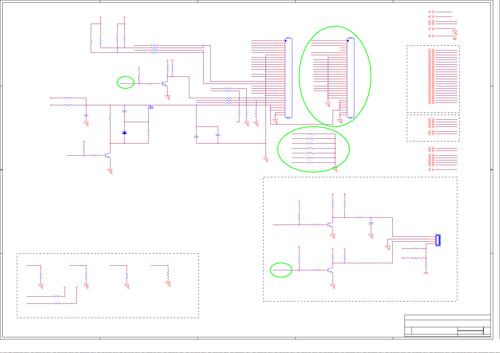
A
21/140
+5VSB
R326
10K/NC
4 4
R338
0R/1206/NC
R/SMD/1206
+5V
R342
+12V
0R/1206/NC
R/SMD/1206
3 3
LO = > LVDS POWER OFF
HI = > LVDS POWER ON
OPCTRL5
CE63
+
220uF/16V
100UF/220UF/SMD
DV33SB
R351
10K
R354
1K
R327
10K/NC
1
R324
10K
R346
1K
Q16
2N3904
SOT23/SMD
3 2
DV33SB
R325
1K
GPIO_16
RA-V3
CB430
1uF/16v
1N4148
1N4148/SMD
1 2
B
LVDS OUT(Include PDP and 32' LCD LVDS interface)
CPUGO /PDPGO :INPUT TO PDP
IRQ /READY :P DP IN PU T T O MT8202
R328 0R/NC
A6N
ADD1
R329 0R
A6P
R330 0R/NC
ADD2 PDPGO
R331 0R/NC
+5VSB
10K
R334
D47
DV33
R335
4.7K
AP2305AN
1
R347
100K
R332
4.7k/NC
1
23
QF3
SOT23/SMD
LVDSVDD
CPUGO
DV33SB
Q15
2N3904
SOT23/SMD
3 2
R333
4.7k
Dim#
Dimming
DISPEN_PDWN_READY
OSCL0
OSDA0
CE64
+
470uF/16v
C470UF16V/D8H9G
R336 0R/NC
R337 0R/NC
R339 0
R340 100/NC
R341 100/NC
R343
0R/NC
+5V
CB431
0.1uF
C
R344
D
+5VSB1,2,7,10,11,12,14
DV33SB1,2,5,6,7,10,11,12
RA-V2
A0N
A0P
A1N
A1P
A2N
A2P
CK1N
CK1P
A3N
A3P
A4N
A4P
A5N
A5P
CK2N
CK2P
A7N
A7P
R345
0
0
J9
1
2
3
4
5
6
7
8
9
10
11
12
13
14
15
16
17
18
19
20
21
22
23
24
25
26
27
28
29
30
31
32
FI-SE30P-HF
LVDS/30P/P1.25
Option1
Option2
Option3
Option4
Option5
Option6
Option7
R348 0R/NC
R0603/SMD
R349 0R/NC
R0603/SMD
R350 0R/NC
R0603/SMD
R352 0R/NC
R0603/SMD
R353 0R/NC
R0603/SMD
R355 0R/NC
R0603/SMD
R356 0R/NC
R0603/SMD
Option1
CPUGO
Option2
Option3
Option4
A0N
A0P
A1N
A1P
A2N
A2P
CK1N
CK1P
A3N
A3P
Option5
Option6
Option7
J10
1
2
3
4
5
6
7
8
9
10
11
12
13
14
15
16
17
18
19
20
21
22
23
24
25
26
27
28
29
30
31
32
FI-SE30P-HF/NC
LVDS/30P/P1.0
RA-V2
+12V1
+5V1,2,7,8,9,11
AGND_LVDS1,2,3,4,5,6,7,8,9,10,11,12,14
GND1,2,3,4,5,6,7,8,9,10,11,12,14
A0P5
A0N5
A1P5
A1N5
A2P5
A2N5
CK1P5
CK1N5
A3P5
A3N5
A4P5
A4N5
A5P5
A5N5
A6P5
A6N5
CK2P5
CK2N5
A7P5
A7N5
OPCTRL55
OPCTRL41,5
GPIO_165,7
LVDS SIGNAL
R5
G5
B5
SVM5
GPIO_135
GPIO_145
OPWM15
OPWM25
OSDA05,7
OSCL05,7
ADD21
ADD11
DV331,2,4,5,6,7,11,12,14
AVCC_ADAC5,6
E
+5VSB
DV33SB
+12V
+5V
AGND_LVDS
GND
A0P
A0N
A1P
A1N
A2P
A2N
CK1P
CK1N
A3P
A3N
A4P
A4N
A5P
A5N
A6P
A6N
CK2P
CK2N
A7P
A7N
OPCTRL5
OPCTRL4
GPIO_16
R
G
B
SVM
GPIO_13
GPIO_14
CRT OUTPUT
OPWM1
OPWM2
OSDA0
OSCL0
ADD2
ADD1
DV33
AVCC_ADAC
+5V
DV33
DV33SB
2 2
OPWM1
G BR SVMSVMSVMSVMSVMSVMSVMSVMSVMSVMSVMSVM
R369
R370
75
R0603/SMD
AVCC_ADAC AVCC_ADAC
R373
10K
R0603/SMD
1 1
GPIO_13
GPIO_14
R374
10K
R0603/SMD
R371
75
R0603/SMD
R372 ONLY FOR HSYNCO
R373 ONLY FOR VSYNCO
R372
75
R0603/SMD
R0603/SMD
75
OPCTRL4
RA-V3
DV33SB
R359
10K
R365
10K
R361
4.7k
4.7k
R368
1
1
FOR DEBUG PURPOSE
A
B
C
R358
R357
1K/NC
1K
R360
Dim#
DV33
0
R364
1K/NC
D
Q17
2N3904
3 2
+5V
R363
1K
Q18
2N3904
3 2
DIMMING CONTROL
CB432
1uF/NC
Dimming
BL_ON/OFF
+5V
R362
10k/NC
DV33
R366
10k/NC
BACK LIGHT CIRCUIT
ZhongShan KAWA Electronic Inc.
Title
LVDS OUTPUT
Document Number
Size
Custom
Date: Sheet
R367
0R/NC
MT5371_V07
J11
1
2
3
4
4P2.0mm
DIP4/W/H/P2.0
E
Drawn:
Checked:
<Designer>
<Checker>
13 14Thu r s da y, M arc h 01, 2007
Rev
2
of
Page 24
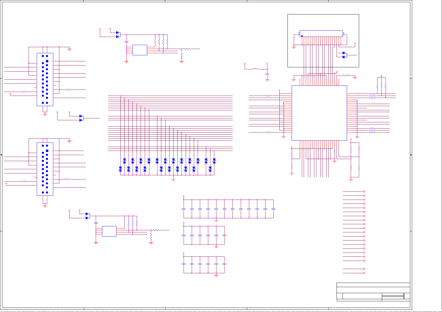
5
22/140
4
3
2
1
Option: Only for HDMI 3
HDMI+5V_A+5VSB
2
3
1
D D
20
P7
RX_A_1+
RX_A_1-
RX_A_C+
RX_A_C-
DDC_SDA_A
HDMI+5V_A
C C
RX_B_1+
RX_B_1-
RX_B_C+
RX_B_C-
DDC_SDA_B
HDMI+5V_B
B B
R4090R
P8
R4110R
21
GND
GND
1
RX2+
2
GND
4
RX1+
6
RX1-
8
GND
10
RXC+
12
RXC-
14
NC
16
SDA
18
+5V
HDMI
2
GND
4
RX1+
6
RX1-
8
GND
10
RXC+
12
RXC-
14
NC
16
SDA
18
+5V
HDMI
3
RX2-
5
GND
7
RX0+
9
RX0-
11
GND
13
CEC
15
SCL
17
GND
19
DET
GND
GND
22
23
20
21
GND
GND
1
RX2+
3
RX2-
5
GND
7
RX0+
9
RX0-
11
GND
13
CEC
15
SCL
17
GND
19
DET
GND
GND
22
23
R410
DDC_SCL_A
0R
HDMI_DET_A
HDMI+5V_AHDMI+5V_B
D85
FHBAT54C
R412
DDC_SCL_B
0R
HDMI_DET_B
+5VSB HDMI+5V_B
RX_A_2+
RX_A_2-
RX_A_0+
RX_A_0-
2
3
1
To MT5371 PIN AJ7
RX_B_2+
RX_B_2-
RX_B_0+
RX_B_0-
2
1
D62
FHBAT54C
PWR5V
3
CB440
0.1uF
1
2
3
FHBAT54C
DDC5V_A
U30
NS/EEPROM 24C04
NC
VCC
NC
WP
NC
SCL
GND4SDA
D61
D63
EDID EEPROM for HDMI 2
A A
DDC5V_A
CB439
0.1uF
U29
NS/EEPROM 24C04
1
NC
VCC
2
NC
WP
3
NC
SCL
GND4SDA
EDID EEPROM for HDMI 1
D64 D66
8
7
6
5
D68
D70
D65
D69
D67
R41847K
R42020K
R41947K
WP_B
DDC_SCL_B
DDC_SDA_B
8
R41447K
R41347K
D71
33
R422
0R/NC
R421
R41520K
DDC_SCL_A
DDC_SDA_A
D73
D75
D72
D74
GPIO_8
7
6
5
R416
WP_A GPIO_8
33
R417
0R/NC
D81
D79
D77
D78
DV33H
DV33H
DV33H
CB441 0.1uF
CB453 10nF
CB459 1nF
D80
CB442 0.1uF
CB454 10nF
CB460 1nF
D76
CB443 0.1uF
CB455 10nF
CB461 1nF
L75
FB/70R/500m A/ 0603
HDMI_DET_B
DDC_SDA_B
DDC_SCL_B
RX_B_CRX_B_C+
RX_B_0RX_B_0+
RX_B_1RX_B_1+
RX_B_2RX_B_2+
HDMI_DET_A
CB449 0.1uF
CB450 0.1uF
DV33H
+
CE14
100uF/16V
100UF/220UF/SMD
R423
1K
R424
1K
CB452 0.1uF
CB451 0.1uF
DV33H
R425
10K/NC
R426
10K/NC
DV33
RX_A_C+
RX_A_CRX_A_0+
RX_A_0RX_A_1+
RX_A_1RX_A_2+
RX_A_2-
DDC_SCL_A
DDC_SDA_A
HDMI_DET_A
RX_B_C+
RX_B_CRX_B_0+
RX_B_0RX_B_1+
RX_B_1RX_B_2+
RX_B_2-
DDC_SCL_B
DDC_SDA_B
HDMI_DET_B
D82
D84
D83
CB444 0.1uF
CB456 10nF
CB462 1nF
CB445 0.1uF
CB457 10nF
CB463 1nF
CB446 0.1uF
CB458 10nF
CB464 1nF
CB447 0.1uF
CB448 0.1uF
P9
NC/FPC/20P/0.5mm/H
21 22
123456789
RX_C_2+
58
59
60
NC
61
GND_10
VCC_9
62
HPD2
63
SDA2
64
SCL2
65
GND_11
66
GND_12
67
B21
68
A21
69
VCC_10
70
B22
71
A22
72
GND_13
73
B23
74
A23
75
VCC_11
76
B24
77
A24
78
GND_14
79
VCC_12
80
HPD1
PC01SDA12SCL13GND_14B115A116VCC_17B128A129GND_210B1311A1312VCC_213B1414A1415GND_316VCC_317VSADJ18PRE19PC1
DV33H
PC0
DDC_SDA_A
DDC_SCL_A
1011121314151617181920
DDC_SDA_C
RX_C_1-
RX_C_2-
RX_C_1+
55
56
B3457A34
VCC_8
DDC_SCL_C
RX_C_C+
RX_C_0-
RX_C_C-
RX_C_0+
47
53
49
52
46
50
B3148A31
B3251A32
B3354A33
GND_9
VCC_7
GND_8
SCL3
U31
PS201/PS301
RX_A_0-
RX_A_2+
RX_A_1-
RX_A_1+
RX_A_0+
RX_A_C+
RX_A_C-
RX_A_2-
45
HDMI_DET_C
SDA3
R427
DV33H
44
HPD3
42
43
VCC_6
SDA_SINK
4.12K
OE*
SCL_SINK
2
1
D86
NC/FHBAT54
R441
30K/NC
41
NC
HPDSINK
GND_7
GND_6
Z1
Y1
VCC_5
Z2
Y2
GND_5
Z3
Y3
VCC_4
Z4
Y4
GND_4
NC
S2
S1
20
R428
10K/NC
PC1
R429
10K
RXCB
RXC
RX0B
RX0
RX1B
RX1
RX2B
RX2
OSDA1
OSCL1
GPIO_2
GPIO_3
GPIO_4
GPIO_5
GPIO_8
AV33
PWR5V
+5VSB
GND
DV33
3
40
39
38
37
36
35
34
33
32
31
30
29
28
27
26
25
24
23
22
21
DV33H
+5VSB
PWR5V
HDMI_DET
R437 33R
DDC_SDA
R436 0R
DDC_SCL
R435 0R
RXC- RXCB
RXC+ RXC
DV33H
RX0- RX0B
RX0+ RX0
RX1- RX1B
RX1+ RX1
DV33H
RX2- RX2B
RX2+ RX2
R434 0R/NC
R433 0R
R432 0R
R430
10K/NC
R431
10K/NC
RXCB 5
RXC 5
RX0B 5
RX0 5
RX1B 5
RX1 5
RX2B 5
RX2 5
OSDA1 5
OSCL1 5
GPIO_2 5
GPIO_3 5,6
GPIO_4 5,6
GPIO_5 5,6
GPIO_8 5, 10
AV33 2,6,10,11
PWR5V 5
+5VSB 1,2,7,10,11,12,13
GND 1,2,3,4,5 , 6,7, 8,9, 10,11, 12,13
DV33 1,2,4,5,6, 7,11, 12,13
DV33
R438 4.7K
R439 47K
R440 47K
GPIO_2
OSDA1
OSCL1
CLOCKCLOCK+
DATA0DATA0+
DATA1DATA1+
DATA2DATA2+
GPIO_5
GPIO_4
GPIO_3
KAWA Confidential
<Designer>
<Checker>
14 14Thur s day, M arch 01, 2007
Rev
2
of
Drawn:
Checked:
1
ZhongShan KAWA Electronic Inc.
Title
HDMI SWITCH
Document Number
Size
MT5371_V08
C
Date: Sheet
5
4
3
2
Page 25

Basic operation of TFT-LCD
23/140
1. After turning on power switch, PSU board sends 5Vst-by Volt to Main
IC MT5371 waiting for ON signals from Key Switch or Remote Receiver.
2. When the ON signal from Key Switch or Remote Receiver is detected, MT5371 will send
ON Control signals to Power. Then Sub PSU sends 5Vsc, 9Vsc, 24V to PCBs working.
3. If some abnormal signals are detected (for example: over volts, over current, over
temperature and under volts), the system will be shut down by Power off.
Page 26

Main IC Specifications
24/140
- MT537x Application Note
- MT5112BD
- CE2836
24-bit, 192KHz. CODEC: 6 ch DAC, 5 Input Mux Stereo ADC
- R2S15102NP
Digital Power Amplifier R2S15102NP
Page 27
25/140
Page 28
26/140
Page 29
27/140
Page 30
28/140
Page 31

29/140
Page 32

30/140
Page 33

31/140
Page 34

32/140
Page 35

33/140
Page 36

34/140
Page 37

35/140
Page 38

36/140
Page 39

37/140
Page 40

38/140
Page 41

39/140
Page 42

40/140
Page 43

41/140
Page 44

42/140
Page 45

43/140
Page 46

44/140
Page 47

45/140
Page 48

46/140
Page 49

47/140
Page 50

48/140
Page 51

49/140
Page 52

50/140
Page 53

51/140
Page 54

52/140
Page 55

53/140
Page 56

54/140
Page 57

55/140
Page 58

56/140
Page 59

57/140
Page 60

58/140
Page 61

59/140
Page 62

60/140
Page 63

61/140
Page 64

Microelectronics
62/140
CE2836
24-bit, 192 KHz. CODEC: 6 Ch DAC, 5 Input Mux Stereo ADC
DESCRIPTION
The CE2836 is a mixed signal CMOS monolithic audio
Codec. It contains six multi-bit sigma delta DAC and a
stereo ADC with 5 input multiplexer, Ideal for audio
playback and recording applications.
The DAC consists of 128-time interpolation filters, 3
order multi-bit Σ∆ modulators, switch capacitors and
analog reconstruction filters. The Σ∆ converter offers
superior differential linearity, with minimum distortion due
to component mis-match. high tolerance to clock jitter.
Additionally it includes separated digital volume control
for each channel.
The ADC utilizes cascaded Σ∆ architecture. The internal
digital filter has a 20K bandwidth. It support sampling
frequency up to 96K Hz. The ADC also includes a analog
Automatic Level Control and Noise Gate function to ease
the recording applications.
ADFS ADXCK
DOUT
ADBCK
SDA
FEATURES
• Six Channel Audio DAC.
- 104 dB SNR (A
Weighted).
- -82 dB THD + N Ratio (A Weighted).
- 32K - 192 KHz. Sampling Rates.
- On -chip Reconstruction Filters.
rd
- Independent Digital Volume Control.
• Stereo Audio ADC.
- 5 Channel ADC inputs.
- Up to 96K Sampling Rate.
- With Automatic Level Control and Noise Gate.
- Includes ALC and Noise Gate Functions.
2
• I
S, Left and Right Justified Digital I/F Formats.
• 2-wire Serial Control Interface.
• 3.3 Volt Power Supply.
Applications
• Digital Surround Sound For Home Theatre
• DVD or DVD Recordable.
SCL
DIN1 DABCK DIN3 DIN2 DAFS DAXCK
ADC CK
CE2836
777
1
R
N
I
A
ADC SIF
OFP
S
L
R
O
777
5
R
N
I
A
E
R
T
T
S
I
N
G
O
E
C
R
C
A
D
7
5
L
N
I
A
777
3
L
O
A
C
D
A
ALC
7
1
L
N
I
A
7
7
7
2
R
N
I
A
7
7
7
3
2
L
R
N
N
I
I
A
A
7
7
7
3
L
N
I
A
7
7
7
4
4
L
R
N
N
I
I
A
A
DAC SIFC I F
DAC 6 CHANNEL
GAIN CONTROL
INTERPOLATION
FILTER
C
A
D
7
3
R
O
A
777
2
L
O
A
DAC CK
C
A
D
7
2
R
O
A
777
1
L
O
A
7
1
R
O
A
Page 65

CE2836 Performance
63/140
CE2836
Item
1 Audio Output Level 1 Vrms
2 Audio Bandwidth 20Hz - 20 KHz +/- 0.1 dB
3 SNR (A-weight) >104 dB
4 THD + NOISE (A-weight, 0 dB input) < -82 dB
5 Dynamic Range 94 dB
6 Channel Separation < -92 dB
7 Nonlinear Distortion < 0.25 dB
8 Channel Gain Error < 0.1 dB
DAC PERFORMANCE SPECIFICATIONS
ADC PERFORMANCE SPECIFICATIONS
1 Maximum Input Level 4 Vpp
2 0 dB Audio Input Level 1 Vrms
3 Audio Bandwidth 20Hz - 20 KHz +/- 0.5 dB
4 SNR (A-weight) >98 dB
5 THD + NOISE (A-weight, 0 dB input) < -88 dB
Spec.
6 Dynamic Range 94 dB
7 Channel Separation < -96 dB
8 Nonlinear Distortion < 0.25 dB
9 Channel Gain Error < 0.5 dB
All Measurement were taken with only one channel active.
Page 66

CE2836
64/140
Description (continue)
The DAC support conversion rate from 32K to 192KHz while the ADC from 32K to 96K. The CE2836 support 32, 24, 20 and
16-bit input data. It also support multiple sampling frequency data. Each DAC has its own individual volume control.
XCK REQUIREMENT
The CE2836 supports 32K, 44.1K, 48K, 96K and 192K sampled audio in DAC operations and32K, 44.1K, 48K and 96K
sampled audio in ADC operations. The oversampled clock, XCK, requirements are listed in Table 1 and 2.
The DAC and ADC PCM serial port can be configured as ‘Master’ or ‘Slave’ independently and each has separated over
sampling clock input. In the ‘Slave Mode’ PCM serial port operation if the AUTODEC, CR1[7]==1,there is an clock
frequency detection circuit to set up the system clock, the users don’t need to set the SRC registers. However in the ‘master
mode’ operation the users need to set the SCR registers for the serial audio clock generations
Table 1.
Sampling
Rate
XCK Freq 12.288 MHz 8.192 Mhz. 24.576 Mhz 16.384 Mhz
32 K
44.1K
48 K
96 K
192 K
All the XCK clock rate listed are supported in the ‘Slave Mode’
SRC Registers are used in the ‘Master Mode’. (#) are not supported in the in the ‘Master Mode’ .
DAC AUTODET is CREG1[7], DAC SRC[1:0]are CREG1[6:5] and DACDIV is CREG1[4].
SRC[1:0] [11], 384 fs (#), 256 fs [11], 768fs (#), 512 fs
XCK Freq 16.934 Mhz 11.29 Mhz. 33.869 Mhz 22.579 Mhz
SRC[1:0] [11], 384fs [10], 256 fs [11], 768 fs [10], 512fs
XCK Freq 18.432 MHz 12.288 Mhz 36.864 MHz 24.576 Mhz.
SRC[1:0] [11], 384 fs [10], 256 fs [11], 768fs [10], 512 fs
XCK Freq 18.432 MHz 12.288 Mhz. 36.864 MHz 24.576 Mhz.
SRC[1:0] [01], 192 fs [00], 128 fs [01], 384 fs [00], 256 fs
XCK Freq 18.432 Mhz 12.288 Mhz. 36.864 MHz 24.576 Mhz.
SRC (#), 96 fs (#), 64 fs (#), 192 fs (#), 128 fs
DAC XCK Requirement
DACDIV==0 DACDIV==1
Page 67

Table 2.
65/140
CE2836
Sampling
Rate
XCK Freq 12.288 MHz 8.192 Mhz. 24.576 Mhz 16.384 Mhz
32 K
44.1K
48 K
96 K
All the XCK clock rate listed are supported in the ‘Slave Mode’ .
SRC Registers are used in the ‘Master Mode’. (#) are not supported in the ‘Master Mode’ .
ADC AUTODETis CREG9[7], DAC SRC[1:0]are CREG9[6:5] and DACDIV is CREG9[4].
SRC[1:0] [10], 384 fs (#), 256 fs [10], 768fs (#), 512 fs
XCK Freq 16.934 Mhz 11.29 Mhz. 33.869 Mhz 22.579 Mhz
SRC[1:0] [10], 384fs [00], 256 fs [10], 768 fs [00], 512fs
XCK Freq 18.432 MHz 12.288 Mhz 36.864 MHz 24.576 Mhz.
SRC[1:0] [10], 384 fs [00], 256 fs [10], 768fs [00], 512 fs
XCK Freq 18.432 MHz 12.288 Mhz. 36.864 MHz 24.576 Mhz.
SRC[1:0] [11], 192 fs [01], 128 fs [11], 384 fs [01], 256 fs
ADC XCK Requirement
DACDIV==0 DACDIV==1
Page 68

PIN ASSIGNMENT
66/140
CE2836
DIN1
DIN2
DIN3
DOUT
VDD
GND
ADFS
ADBCK
ADXCK
GND
N/C
AINR5
10
11
12
K
K
C
S
F
A
D
8
4
1
2
3
4
5
6
7
8
9
3
1
5
L
N
I
A
C
X
B
A
D
7
4
A
L
A
D
D
S
6
5
4
4
C
/
C
N
S
4
3
4
4
CE2836
4
5
6
7
1
1
1
C
/
N
4
4
L
R
N
N
I
I
A
A
8
1
1
3
3
L
R
N
N
I
I
A
A
H
H
V
C
A
/
D
N
2
1
4
4
9
0
1
2
2
2
L
R
N
N
I
I
A
A
L
V
V
A
A
D
D
0
9
4
3
1
2
2
2
1
1
L
R
N
N
I
I
A
A
M
L
C
V
V
A
A
D
D
8
7
3
3
AOR1
36
AOL1
35
AOR2
34
AOL2
33
AOR3
32
AOL3
31
AVDD
30
AGND
29
ADVCM
28
AGND
27
ADVRF
26
AGND
25
3
4
2
2
C
A
/
D
N
D
V
PIN DESCRIPTION
Pin Name Pin # Type Description
DIGITAL
N/C 43 No connection. It can be tied to GND.
SDA 44 I/O Serial command port data line.
SCL 45 I Serial command port clock line.
DAXCK 46 I External master clock input for DAC.
DABCK 47 I DAC audio serial data clock
Input pin (default) if DAC I/F is configured to be ‘slave’ else it is an Output.
DAFS 48 I DAC left/right channel clock pin. Please refer to Figure 1 PCM data format for its
definition
Input (default) if DAC I/F is configured to be ‘slave’ else it is an output
DIN1 1 I DAC Channel 1 or TDM serial audio data input.
DIN2 2 I DAC Channel 2 serial audio data input.
Page 69

CE2836
67/140
PIN DESCRIPTION (Continued)
Pin Name Pin # Type Description
DIN3 3 I DAC Channel 3 serial audio data input.
DOUT 4 O Serial ADC output
VDD 5 +3.3V Digital power supply, 3.3 Volt.
GND 6 GND Digital ground
ADFS 7 I/O ADC left/right channel clock pin. Please refer to Figure 1 PCM data format for its
definition.
Input (default) if ADC I/F is configured to be ‘slave’ else it is an output
ADBCK 8 I/O External master clock input for ADC.
Input (default) if ADC I/F is configured to be ‘slave’ else it is an output
ADXCK 9 I ADC audio serial data clock input.
GND 10 I Digital ground
Analog
N/C 11 No connection. It can be tied to AGND.
AINR5 12 I ADC channel 5 right input. Input resistance is 20K Ohm
AINL5 13 I ADC channel 5 left input. Input resistance is 20K Ohm
N/C 14 No connection. It can be tied to AGND.
AINR4 15 I ADC channel 4 right input. Input resistance is 20K Ohm
AINL4 16 I ADC channel 4 left input. Input resistance is 20K Ohm
AINR3 17 I ADC channel 3 right input. Input resistance is 20K Ohm
AINL3 18 I ADC channel 3 left input. Input resistance is 20K Ohm
AINR2 19 I ADC channel 2 right input. Input resistance is 20K Ohm
AINL2 20 I ADC channel 2 left input. Input resistance is 20K Ohm
AINR1 21 I ADC channel 1 right input. Input resistance is 20K Ohm
AINL1 22 I ADC channel 1 left input. Input resistance is 20K Ohm
AVDD 23 +3.3V ADC power supply.
N/C 24 No connection. It can be tied to AGND.
AGND 25 GND Analog ground pin.
ADVRF 26 O ADC reference voltage. It should be decoupled to AGND with a 22 uF capacitor in
parallel with a 0.1 uF. Its value should be AVDD/2 volt.
AGND 27 GND Analog ground pin.
Page 70

CE2836
68/140
PIN DESCRIPTION (Continued)
Pin Name Pin # Type Description
ADVCM 28 O ADC comment mode voltage. It should be decoupled to AGND with a 22 uF in parallel
with a 0.1 uF. Signal level is AVDD/2.
AGND 29 GND Analog ground pin.
AVDD 30 +3.3V DAC power supply.
AOL3 31 O Analog left channel 3 output
AOR3 32 O Analog right channel 3 output
AOL2 33 O Analog left channel 2 output
AOR3 34 O Analog right channel 2 output
AOL1 35 O Analog left channel 1 output
AOR1 36 O Analog right channel 1 output
DAVCM 37 O DAC comment mode voltage. It should be connected to a 22 uF in parallel with a 0.1 uF
decoupling capacitors to ground. Signal level is AVDD/2.
DAVL 38, 39 GND DAC negative reference voltage. It should be tied to AGND.
DAVH 40,41 I DAC positive reference voltage. It should be connected to AVDD via a 180 ohm serial
resistor, and a 22 uF in parallel with a 0.1 uF decoupling capacitors to ground.
N/C 42 No connection. It can be tied to AGND.
Page 71

CE2836
69/140
DIGITAL AUDIO SERIAL INTERFACE
There are two independent PCM serial ports, one for DAC and one for ADC. The DAC digital serial interface consists of 3
serial input pins, DIN1, DIN2, DIN3, one serial clock input/output pin, DABCK, and one left/right indicator input/output pin,
DAFS. The ADC consists of a data output pin, DOUT and one serial clock input/output pin, ADBCK, and one left/right
indicator input/output pin, ADFS. The BCK and FS are output pins when the respective port is configured as ‘Master’, and
input pin when it is configured as ‘Slave’ port. The Master/Slave operations are setup via CREGA[7] and CREGA[3]. The
data are 2’s complement MSB first numbers. The CE2836 supports four resolution, which are selected programming the
control register CREG0 and CRFEGA via the I
Table (3): Audio Serial Data Input Resolution,
The DIN and DOUT can be either 24-bit or 32-bit per frame as well as left justified, right justified or I2S. .
2
C serial control port. Table 3 describes these four resolution.
Format NBIT[1:0] DIN, DOUT
0 00 16-bit
1 01 20-bit
2 10 24-bit (default)
3 11 32-bit
Table (4): Audio Serial Data Input Modes
Mode FMT[1:0] DIN, DOUT
0 00 Right Justified
1 01 Left Justified
2 10 I2S (default)
311TDM
TDM Input Format
The CE2836 support Time Division Multiplex data input. In this format only one data input pin is required. The six channel
data are sent in serial order, channel 1 first, followed by channel 2 and so forth. The number of bits per channel is defined by
CREG0[5:4].
Page 72

FS
70/140
BCK
CE2836
Figure 1. Audio Serial Input Data Format
1/fs
left Channel right channel
DIN,DOUT
FS
BCK
DIN,DOUT
FS
BCK
DIN,DOUT
LSBMSB
012
nn
LSBMSB
012
Right Justified Input Format
left Channel right channel
LSBMSB
nn
123
LSBMSB
123
Left Justified Input Format
left Channel right channel
LSBMSB
123
nn
LSBMSB
123
FS
BCK
DIN,DOUT
2
I S Input Format
LSBMSB
12
LSBMSB
123
nnn
LSBMSB
Channel 0 Channel 1 Last Channel
TDM Input Format
12
data = 03
Page 73

CE2836
71/140
DAC INFINITE ZERO DETECTION
The CE2836 DAC has an Infinite Zero Detection circuit which detects zero in the Audio Serial Port that lasts for
approximately 0.2 sec. By default, the zero detection circuit is on.
DAC Digital Attenuation
Each DAC contains an Digital Attenuation block. The attenuation values are hold in the Volume Control Registers. The Value
80H corresponds to Full Scale, 0dB. and each decrement correspond to -0.5 dB additional attenuation.
ADC Gain and ALC
Each channel of ADC input includes a Analog Gain. The Gain is controlled by CREGC, ADC Gain Selection, The gain range
is from +6 dB to -9 dB. with 1 dB step. The GAIN = 9 corresponds to 0dB gain. The AUTOMATIC LEVEL CONTROL set
the ADC maximum digital output to a prescribed value by automatic manipulating the analog gain. The ALC is controlled by
CREG8, ADC PROC. REGISTER..
Table (5): ALC Target Level
ALC[2:0] Maximum Digital Output
000 -1 dB FS
001 -2 dB FS
010 -3 dB FS
011 -4 dB FS
100 -5 dB FS
101 -6 dB FS
110 -7 dB FS
111 -8 dB FS
Table (6): ALC Hold Time
ALCHTM Hold Time Comment
0 340 msec. For music program
1 5.3 msec For speech program
Page 74

CE2836
72/140
ADC Noise Gate
Noise Gate remove hissing noise during silence period. It is useful for recording noisy program. While Noise Gate is enabled
the ADC digital output will be zeroed if the signal level below a predetermined value for about 0.5 seconds. The noise Gate is
controlled by the same ADC PROC. REGISTER.
Table (7): Noise Gate Threshold
NGTH[1:0] Threshold
00 -66 dB
01 -72 dB
10 -78 dB
11 -84 dB
Serial Command Port
The user can select the chip operation mode by programming the internal control registers through serial I2C port. The Chip
Address for the CE2836 is 35H. The protocol for write operation consists of sending 3 byte data to CE2836, following each
byte is the acknowledges generated by CE2836. The first byte is the 7-bit Chip Address followed by the read/write bit (read is
high, write is low). The second byte is the control register address. The third byte is the control register data.
Upon power up, all programmable registers are set to default values. Figure 2 describes the serial command port timing
relationship.
Figure 2. Serial Command Port Timing
I2C Bus Control Register Write Example:
first byte second byte third byte
SDA
SCL
Start StopCA6
11 1
Example
Set channel 1L volume to 30H:
1
first byte: [CA R/W] = 6AH
second byte: register address: A<7:0> = 02H
third byte: data D<7:0> = 30H
CA0
R/W
ACK
A7 A0
( Note: Chip adrress: CA<6:0> = 35H, R/W =0.)
ACK
D7
ACK
D0
Page 75

CE2836
73/140
SERIAL PORT CONTROL REGISTER ASSIGNMENT
There are 8 registers dedicated to the CE2836 for chip functional programming, The register addresses assignments are
Address
(decimal)
0 CREG0[7:0] A0 DAC Control REG0: Data input format, de-emphasis filter
1 CREG1[7:0] 80 DAC Control REG1: Input format and PLL output fre-
2 CREG2[7:0] 80 Volume Control Register for DAC channel 1, left
3 CREG3[7:0] 80 Volume Control Register for DAC channel 1, right
4 CREG4[7:0] 80 Volume Control Registerl for DAC channel 2, left
5 CREG5[7:0] 80 Volume Control Register for DAC channel 2, right
6 CREG6[7:0] 80 Volume Control Register for DAC channel 3, left
7 CREG7[7:0] 80 Volume Control Registerl for DAC channel 3, right
8 CREG8[7:0] 82 ADC Proc REG: ALC and Noise Gate Control Registers
9 CREG9[7:0] A0 ADC Control Register.
10 CREGA[7:0] 00 CHIP Control Register.
11 CREGB[7:0] 01 ADC MUX Select.
Register
Default
Value
Register Function
selection
quency selection
12 CREGC[7:0] 99 ADC Input Gain Select
13 CREGD[7:0] 92 Chip Soft Reset.
Page 76

CONTROL REGISTERS DESCRIPTION
74/140
CREG0, DAC Control Register 0 (ADRS=hex00, default=hexA0)
CREG0[7:0]
ADDR[3:0]
BIT 7 BIT 6BIT 5BIT 4BIT 3BIT 2BIT 1BIT 0
Hex 00 FMT[1:0] NBIT[1:0] AMUTE DEEMP FSMPL[1:0]
Default Value 1 0 1 0 0 0 0 0
FMT[1:0] Digital Serial Bus Format Select
00: - Normal or Right Justified Format.
01: -Left Justified Format.
10: - I2S Format.(default)
11: - TDM, Multi-channel Time Division Multiplex Format
NBIT[1:0]: - These two bits define the serial audio input resolution for right justified and TDM mode
00: - 16-bit resolution.
01: - 20-bit resolution.
10: - 24-bit resolution (default).
11: - 32-bit resolution.
CE2836
AMUTE: - Auto-mute detection enable.
0: - Auto-mute enabled. (default)
1: - No auto-mute.
DEEMP: - Enable de-emphasis
0: - Normal. (default)
1: - enable de-emphasis.
FSMPL: - Interpolation filter selection.
These two bits are recognized only when “AUTODET” bit of the CREG1 is set to ‘0’.
0X: - 44.1 or 48K sampling.(default)
10: - 96K sampling.
11: - 192K sampling.
Page 77

CREG1, DAC Control Register 1(ADRS=hex01, default=hex80)
75/140
CREG1[7:0]
ADDR[3:0]
BIT 7 BIT 6 BIT 5 BIT 4 BIT 3 BIT 2 BIT 1 BIT 0
CE2836
Hex 01
Default Value 1 0 0 0 0 0 0 0
AUTODET
SRC[1:0] CKDIV2 X MUTE56 MUTE34 MUTE12
AUTODET Automatically detects the serial audio input data sampling rate clock frequency.
0: - do not use auto-detect
1: - automatically detects the serial audio input data sampling rate and clock frequency.
SRC[1:0]: - DAC Sampling Rate Selection. It is used in the DAC Master Mode, CRA[7]==1, to generate DAFS and
DABCK.
00: - Sampling Rate = XCK/128.
01: - Sampling Rate = XCK/192.
10: - Sampling Rate = XCK/256.
11: - Sampling Rate = XCK/384.
CKDIV2: - Enable the ADXCK Clock divided by 2.
0: - DAC system clock is DAXCK (default)
1: - DAC system clock is DAXCK/2
MUTE56:
Mute control for channels 5 and 6
0: do not mute channels 5 and 6
1: simultaneously mute channels 5 and 6
MUTE34: Mute control for channels 3 and 4
0: do not mute channels 3 and 4
1: simultaneously mute channels 3 and 4
MUTE12: Mute control for channels 1 and 2
0: do not mute channels 1 and 2
1: simultaneously mute channels1 and2
Page 78

CE2836
76/140
CREG2 - 7, DAC Volume Registers for channel 1 to 6, (ADRS=hex02 - hex07, default=hex80)
Volume Registers
ADDR[3:0]
BIT 7BIT 6BIT 5BIT 4BIT 3BIT 2BIT 1BIT 0
Hex 02 Channel 1 left volume register, VOLREGL1[7:0]
Hex 03 Channel 1 right volume register, VOLREGR1[7:0]
Hex 04 Channel 2 left volume register, VOLREGL2[7:0]
Hex 05 Channel 2 right volume register, VOLREGR2[7:0]
Hex 06 Channel 3 left volume register, VOLREGL3[7:0]
Hex 07 Channel 3 right volume register, VOLREGR3[7:0]
Default Value 10000000
VOLREG:- Control the volume of the 6 DAC’s
80h corresponds to 0 dB and 02h to -64 dB. in -0.5 db step. Value should not be programmed greater than 80h.
Page 79

CREG 8, ADC Proc Register (ADRS=hex08, default=hex82)
77/140
CREG0[7:0]
ADDR[3:0]
BIT 7 BIT 6 BIT 5 BIT 4 BIT 3 BIT 2 BIT 1 BIT 0
CE2836
Hex 08 NGATE NGTH[1:0]
Default Value 1 0 0 0 0 0 1 0
ALCHTM
ALCEN ALC[2:0]
NGATE: Noise Gate
0: - Noise Gate Disabled.
1: -Noise Gate Enable. When the signal level is lower than the level specified by the NGTH the ADC output
will be zeroed.
NGTH[1:0]: - Specified the Noise Gate Threshold.
00: - -66dB
01: - -72 dB.
10: - -78dB.
11: - -84 dB.
ALCHTM: - Automatic Level Control Hold time.
0: - 340 ms. (default). For music program.
1: - 5.3 ms. This should be used for speech conversion.
ALCEN: - Enable Automatic Level Control Function
0: - Disable ALC. (default)
1: - Enable ALC.
ALC[2:0]: - ALC Target Level.
000: - -1 dB.
001: - -2 dB.
010: - -3 dB. (default)
011: - -4 dB.
100: - -5 dB.
101: - -6 dB.
110: - -7 dB.
111: - -8 dB.
Page 80

CREG9, ADC Control Register (ADRS=hex09, default=hexA0)
78/140
CREG0[7:0]
ADDR[3:0]
BIT 7 BIT 6BIT 5BIT 4BIT 3BIT 2BIT 1BIT 0
Hex 09 FMT[1:0] NBIT[1:0] X SRC[1:0] CKDIV2
Default Value 1 0 1 0 0 0 0 0
MT[1:0] Digital Serial Bus Format Select for ADC.
00: - Normal or Right Justified Format.
01: -Left Justified Format.
10: - I2S Format.(default)
11: - TDM, Multi-channel Time Division Multiplex Format
NBIT[1:0]: - These two bits define the ADC serial audio input resolution for right justified and TDM mode
00: - 16-bit resolution.
01: - 20-bit resolution.
10: - 24-bit resolution (default).
11: - 32-bit resolution.
CE2836
SRC[1:0]: - ADC Sampling Rate Selection. It is used in the ADC Master Mode, CRA[1]==1, to generate ADFS and
ADBCK.
00: - Sampling Rate = XCK/256.
01: - Sampling Rate = XCK/128.
10: - Sampling Rate = XCK/384.
11: - Sampling Rate = XCK/192.
CKDIV2: - Enable the ADXCK Clock divided by 2.
0: - ADC system clock is ADXCK (default)
1: - ADC system clock is ADXCK/2
Page 81

CREGA, Chip Control Register (ADRS=hex0A, default=hex00)
79/140
CREG1[7:0]
ADDR[3:0]
BIT 7 BIT 6 BIT 5 BIT 4 BIT 3 BIT 2 BIT 1 BIT 0
CE2836
Hex 0A
Default Value 0 0 0 0 0 0 0 0
DAMSTR
DAPWD X X ADMSTR ADPWD ZCBYP HPFBYP
DAMSTR: Configure the DAC PCM Serial Port.
0: - Slave Mode
1: - Master Mode.
DAPWD: DAC Power Down
0: DAC enabled
1: DAC Power Down.
ADMSTR: Configure the ADC PCM Serial Port.
0: - Slave Mode
1: - Master Mode.
ADPWD: ADC Power Down
0: ADC enabled
1: ADC Power Down.
ZCBYP: Disable ADC Zero Crossing Detection
0: Zero crossing is enabled.
1: Zero crossing is bypassed.
HPFBYP: Bypass ADC data path High Pass Filter
0: Enable high pass filter.
1: Disable high pass filter.
Page 82

CREGB, ADC Input Enable (ADRS=hex0B, default=hex01)
80/140
CREG1[7:0]
ADDR[3:0]
BIT 7 BIT 6 BIT 5 BIT 4 BIT 3 BIT 2 BIT 1 BIT 0
Hex 0B X X X AMUX[4:0]
Default Value 1 0 0 0 0 0 0 1
AMUX[4:0]: ADC Input Channel Enable.
00001: - AIN1
00010: - AIN2
00100: - AIN3
01000: - AIN4
10000: - AIN5
CREGC, ADC Input Gain Selection (ADRS=hex0C, default=hex99)
CREG1[7:0]
ADDR[3:0]
BIT 7 BIT 6 BIT 5 BIT 4 BIT 3 BIT 2 BIT 1 BIT 0
CE2836
Hex 0C LGAIN[3:0] RGAIN[3:0]
Default Value 1 0 0 1 1 0 0 1
LGAIN[3:0] is for ADC Left Channel Gain Select While RGAIN[3:0] is for Right Channel Gain Select
1111 corresponds to +6 dB and 0000 to -9 dB with -1dB step
CREGD, Chip Soft Reset (ADRS=hex0D, default=hex92)
CREG1[7:0]
ADDR[3:0]
BIT 7 BIT 6 BIT 5 BIT 4 BIT 3 BIT 2 BIT 1 BIT 0
Hex 0D RESET[7:0]
Default Value 1 0 0 1 0 0 1 0
Chip Soft Reset; A write of all zeros to this register will reset the chip except the Command Registers.
Another write of hex92 is required to enable to chip again.
Page 83

APPLICATION CONNECTION EXAMPLE:
81/140
Analog
3.3 Volt
100 uF
CE2836
180 Ohm
Digital
3.3 Volt
+3.3 Volt
680 ohm
2
I C Serial
Interface
Over Sample Clock
Digital Audio
Interface
Over Sample Clock
All Unmarked
Capacitors have
values of 0.1 uF
22 uF
44
45
46
47
48
AVDD
23
DAVH
30
5
DVDD
6
DGND
CE2836
SCL
SDA
DAXCK
DABCK
DAFS
1
DIN1
2
DIN2
3
DIN3
4
DOUT
7
ADFS
8
ADBCK
9
ADXCK
14
24
N/C
42
25
27
AGND
4041
DAVL
AOR1
AOL1
AOR2
AOL2
AOR3
AOL3
AINL1
AINR1
AINL2
AINR2
AINL3
AINR3
AINL4
AINR4
AINL5
AINR5
39
38
36
35
34
33
32
31
22
21
20
19
18
17
16
15
13
12
220 uF
10 uF
10 uF
10 uF
10 uF
10 uF
10 uF
10 uF
10 uF
10 uF
10 uF
10 uF
10 uF
10 uF
10 uF
10 uF
10 uF
29
22 uF
DAVCM
ADVRF
37
22 uF
26
ADVCM
28
22 uF
Page 84

CE2836
82/140
SUGGESTED ANALOG RECONSTRUCTION FILTER
A second Sallen Key low pass reconstruction filter is recommend to remove the high frequency sigma delta modulator noise.
The filter’s component values and characteristic are shown in the following figures.
Sallen Key 2nd order LP filter
1000 pF
4.7 uF
100 K
5
0
-5
-10
-15
Amplitude (dB)
-20
2.7 K
10 K
680 pF
LPF Frequency Res ponse
+
-
10 K
10 K
All resistors and capicitors are
5% precision.
-25
-30
10
3
10
4
Freq (Hz.)
10
5
Page 85

CE2836
83/140
ADC
The ADC converters have a input buffer. The buffers have a equivalent input resistance of 20K ohm. To ensure the
performance it is recommended that the applications should have a simple low pass filter to remove the high frequency noise.
Recommended ADC
input circuits
20 K
5.1 K
100 pf
1 uf
5.1 K
20 K
VCM
ADC
Internal Buffer
Page 86

TIMING DIAGRAM
84/140
BCK
DIN,
DOUT
FS
Figure 3. Audio Serial Interface Timing Requirement
tbck
tbck
L
tkd
su
tkr
su
tkr
tbck
hd
H
CE2836
tkd
hd
SDA
SCL
Figure 4. Serial Command Port Write Timing Requirement
tSCL
tLOW
SDA, SCL
tF tR
tBF tHD,sta
stop start stopstart
tHD,dat tSU,dat tSU,sta tSU,stp
tHIGH
Page 87

CE2836
85/140
ABSOLUTE MAXIMUM RATINGS
Symbol Characteristics Min Max Units
V
DD
V
i
A
i
V
o
A
o
TDsc
TA
SC
T
a
T
j
Tsol Lead Soldering Temperature (10 sec., 1/4” from pin) 280
Tvsol Vapor Phase Soldering (1 minute) 220
Tstor Storage Temperature -65 +150
Power Supply Voltage (Measured to GND) -0.5 +7.0 V
3,4
2
3,4
GND-0.5 V
-100 100 mA
2
GND-0.5 VDD+0.5 V
-100 100 mA
1Sec
Digital Input Applied Voltage
Digital Input Forced Current
Digital Output Applied Voltage
Digital Output Forced Current
Digital Short Circuit Duration (single output high state to Vss)
Analog Short Circuit Duration (single output to VSS1) infinite Sec
Ambient Operating Temperature Range -25 +125
Junction Temperature (Plastic Package) -65 +150
o
C
o
C
o
C
o
C
o
C
Notes:
1. Absolute maximum ratings are limiting values applied individually, while all other parameters are within specified
operating conditions.
2. Applied voltage must be current limited to specified range, and measured with respect to VSS.
3. Forcing voltage must be limited to specified range.
4. Current is specified as conventional current, flowing into the device.
Page 88

CE2836
86/140
ELECTRICAL CHARACTERISTICS
Parameter Characteristics Min Typ Max Units
Power Supply
AVDD Analog power supply voltage 2.8 3.3 4.0 V
DVDD Digital power supply voltage 2.8 3.3 4.0 V
I
I
DA
DD
Analog Current 60 mA
Digital Current 20 18 mA
Audio DAC Characteristics
Full Scale Output Voltage to a 10K load .98 1 1.02 Vrms
V
VCM
Reference voltage VDD/2 V
Digital Characteristics
V
IH
Digital Input Voltage, Logic HIGH,
TTL Compatible Inputs.
I
OZH
I
OZL
C
C
I
O
Hi-Z Leakage Current, HIGH,
=Max, VIN=3.3 Volt
V
DD
Hi-Z Leakage Current, LOW,
=Max, VIN=V
V
DD
Digital Input Capacitance (TA=25oC, f=1Mhz) 8 pF
Digital Output Capacitance (TA=25oC, f=1Mhz) 10 pF
SS)
2.0 V
DD
33 A
-10 A
V
µ
µ
Audio Serial Interface Timing
tbck
tbck
tbck
tkd
H
L
su
BCK Cycle Time 80 ns
BCK Pulse Width, HIGH 30 ns
BCK Pulse Width, LOW 30 ns
Audio Data Setup Time With Respect To Rising
Edge of BCK
tkd
hd
Audio Data Hold Time With Respect to Rising
Edge of BCK
tkr
su
Audio FS Setup Time With Respect To Rising
Edge of BCK
10 ns
15 ns
10 ns
Page 89

CE2836
87/140
Parameter Characteristics Min Typ Max Units
tkr
hd
Serial Command Port
Audio FS Hold Time With Respect To Rising
Edge of BCK
15 ns
fSCL SCL Clock Frequency 100 kHz
tSU,sta Start condition set up time 4.7 us
tHD,sta Start condition hold time 4.0 us
tSU,stp Stop condition set up time 4.0 us
tLOW SCL Low time 4.7 us
tHIGH SCL High time 4.0 us
tR SCL & SDA rise time 1.0 us
tF SCL & SDA fall time 0.3 us
tSU,DAT Data set-up time 250 ns
tHD,DAT Data hold time 0 ns
tBF Bus Free time 4.7 us
Page 90

PACKAGING INFORMATION (LQFP 48 PIN)
88/140
CE2836
Dimensions
SYMBOLS
mm.
SYMBOLS
mm.
min norm max min norm max
A
A1
0.05 0.15
1.68
A2 1.35 1.4 1.45
b 0.17 0.22 0.27
C 0.09 0.20
D
D1
48
1
e
b
37
2939
28
9.0 BSC
7.0 BSC
LQFP 48 (7 X 7 mm)
36
E
E1
e
L
L1
9.0 BSC
7.0 BSC
0.45 0.65 0.75
0.63 0.6 1.03
1.00 REF
12
7
13
E1
D1 D
24
18
17
E
c
L
L1
A2
A1
A
Page 91

89/140
Page 92

90/140
Page 93

91/140
Page 94

92/140
Page 95

93/140
Page 96

94/140
Page 97

95/140
Page 98

Issued Date: Nov. 17, 2006
96/140
Model No.: V260B1 - L01
TFT LCD Approval Specification
MODEL NO.: V260B1 - L01
Approval
Page 99

Issued Date: Nov. 17, 2006
97/140
Model No.: V260B1 - L01
1. GENERAL DESCRIPTION
1.1 OVERVIEW
V260B1- L01 is a TFT Liquid Crystal Display module with 12-CCFL Backlight unit and 1ch-LVDS
interface. The displ ay diagonal is 26”. This module supports 1366 x 768 W XGA format and can display
16.2M colors(6-bits+FRC colors). The inverter module for backlight is built-in.
Approval
1.2 FEATURES
- Excellent brightness 500n its
- Contrast ratio 800:1
- Fast response time (8ms)
- Color saturation NTSC 72%
- WXGA (1366 x 768 pixels) resolution
- DE (Data Enable) only mode
- LVDS (Lo w Voltage Differential Signaling) int erface
- Viewing angle: 160(H)/150(V) (CR>10) TN technology
-Color reproduction (Nature color)
- RoHS compliance
1.3 AP PL ICATION
- TFT LCD TVs
- High brightness, multi-media displays
1.4 GENERAL SPECIFICA T I0NS
Item Specification Unit Note
Active Area 575.769 (H) x 323.712 (V) (26” diagonal) mm
Bezel Opening Area 580.8 (H) x 328.8 (V) mm
Driver Element a-si TFT active matrix -
Pixel Number 1366 x R.G.B. x 768 pixel
Pixel Pitch (Sub Pixel) 0.1405 (H) x 0.4215 (V) mm
Pixel Arrangement RGB vertical stripe -
Display Colors 16.2M color
Display Operation Mode Transmissive mode / Normally White -
Surface Treatment
Anti-Glare coating (Haze 25%)
Hard coating (3H)
-
(1)
1.5 MECHA N ICAL SPECIFICATIONS
Item Min. Typ. Max. Unit Note
Horizontal(H) 625 626 627 mm
Module Size
Note (1) Please refer to the attached drawings for more information of front and back outline dimensions.
Vertical(V) 372 373 374 mm
Depth(D) 35.6 36.6 37.6 mm To PCB cover
Depth(D) 41.2 42.2 43.2 mm To inverter cover
Weight -- 4500 -- g
Version 2.1
Page 100

Issued Date: Nov. 17, 2006
98/140
Model No.: V260B1 - L01
Approval
2. ABSOLUTE MAXIMUM RATINGS
2.1 ABSOLUTE RATINGS OF ENVIRONMENT
Item Symbol
Storage Temperature TST -20 +60 ºC (1)
Operating Ambient T emperature TOP 0 +50 ºC (1), (2)
Shock (Non-Operating) S
Vibration (Non-Operating) V
Note (1) Temperature and relative humidity range is shown in the figure below.
(a) 90 %RH Max. (Ta ≦ 40 ºC).
(b) Wet-bulb temperature should be 39 ºC Max. (Ta > 40 ºC).
(c) No condensation.
Note (2) The maximum operating temperature is based on the test condition that the surface temperature of
display area is less than or equal to 60 ºC with LCD module alone in a temperature controlled chamber.
Thermal management should be considered in final product design to prevent the surface temperature of
- 50 G (3), (5)
NOP
- 1.0 G (4), (5)
NOP
Min. Max.
Value
Unit Note
display area from being over 60 ºC. The range of operating temperature may degrade in case of improper
thermal management in final product design.
Note (3) 11 ms, half sine wave, 1 time for ± X, ± Y, ± Z.
Note (4) 10 ~ 500 Hz, 10 min, 1 time each X, Y, Z.
Note (5) At testing Vibra tion a nd Shoc k, the f ixture in hold ing the m odule has to be har d and rigi d enough
so that the module would not be twisted or bent by the fixture.
Relative Humidity (%RH)
100
90
80
60
Operating Range
40
20
10
Storage Range
-40 40-20 0 20 60 80
Temperature (ºC)
Version 2.1
 Loading...