

Page 1

DVD PLAYER
Model:
A5181
SERVICE MANUAL
www.akai.ru
Page 2

Terminology & Abbreviations
Terminology & Abbreviations
AC-3 The former name of the Dolby Digital audio-coding system . AC-3 followed AC-1 and
AC-2. Still used in some standards documents.
Angle In DVD-video, a specific view of a scene, usually recorded from a certain camera
angle. Different angles can be chosen while viewing the scene.
CD Short for compact disc, an optical disc storage format developed by Philips and Sony.
CD-DA Compact disc digital audio. The original music CD format, storing audio
information as digital PCM data. Defined by the Red Book standard.
CD+G Compact disc plus graphics. A variation of CD which embeds graphical data in with
the audio data, allowing video pictures to be displayed periodically as music is
played. Primarily used for karaoke.
CD-R An extension of the CD format allowing data to be recorded once on a disc by using
dye-sublimation technology. Defined by the Orange Book standard.
Channel A part of an audio track. Typically there is one channel allocated for each
loudspeaker.
Chapter In DVD-Video, a division of a title. Technically called a part of title (PTT).
Closed Caption Text captions for video which are not normally visible, as opposed to open
captions, which are a permanent part of the picture. In the United States, the official
NTSC Closed Caption standard requires that all TVs larger than 13 inches include
circuitry to decode and display caption information stored on line 21 of the video
signal. DVD-Video can provide closed caption data, but the subpicture format is
preferred for its versatility.
Component Video A video system containing three separate color component signals, either
red/green/blue (RGB) or chroma/color difference (YGbCr, YPbPr, YUV), in analog
or digital form. The MPEG-2 encoding system used by DVD is based on
color-difference component digital video. Very few televisions have component
video inputs.
Composite Video An analog video signal in which the luma and chroma components are
combined (by frequency multiplexing), along with sync and burst. Also called CVBS.
Most televisions and VCRs have composite video connectors, which are usually
colored yellow.
CD-i Compact disc interactive. An extension of the CD format designed around a set-top
computer that connects to a TV to provide interactive home entertainment, including digital
audio and video, video games, and software applications. Defined by the Green Book
standard. CD-i Assn.
1-1
Page 3

Terminology & Abbreviations
Dolby Digital A perceptual coding system for audio, developed by Dolby Laboratories and
accepted as an international standard. Dolby Digital is the most common means of
encoding audio for DVD-Video and is the mandatory audio compression system for
525/60 (NTSC) discs.
Dolby Surround The standard for matrix encoding surround-sound channels in a stereo
signal by applying a set of defined mathematical functions when combining center
and surround channels with left and right channels. The center and surround channels
can then be extracted by a decoder such as a Dolby Pro Logic circuit which applies
the inverse of the mathematical functions. A Dolby Surround decoder extracts
surround channels, while a Dolby Pro Logic decoder uses tially independent of the
recording or transmission format. Both Dolby Digital and MPEG audio compression
1-1
systems are compatible with Dolby Surround audio.
DTS Digital Theater Sound. A perceptual audio-coding system developed for theaters. A
competitor to Dolby Digital and an optional audio track format for DVD-Video.
DVCD Stands for Double Video CD -- pretty popular format in mainland China.
Format itself is nothing new really, its just a regular VideoCD overburned to include 90 to
99mins per CD, compared to regular 74mins per CD in standard VideoCD format.
DVD An acronym that officially stands for nothing, but is often expanded as Digital Video
Disc or Digital Versatile Disc. The audio/video/data storage system based on 12-and
1-1
8-cm optical discs.
DVD+R DVD+Recordable defines a standard for recordable DVD drives and media defined
by the DVDRW Alliance. Often called "plus R", the format is write once (compared to
DVD+RW wich can be erased and rewritten). The single sided discs can hold 4,700,000,000
bytes (4.38 Gigabytes at 1024 bytes to the kilobyte) with double sided discs holding twice as
much. There are no dual layer single sided recordable discs. This format competes with the
DVD Forum DVD-R specification. DVDRhelp DVDR information
JPEG Joint Photographic Experts Group. The international committee which created its
namesake standard for compressing still images.
Karaoke Literally empty orchestra. The social sensation from Japan where sufficiently
inebriated people embarrass themselves in public by singing along to a music track.
Karaoke was largely responsible for the success of laserdisc in Japan, thus supporting
it elsewhere.
Kodak Picture CD Kodak Picture CD is a CD that contains your pictures in JPEG
format(.jpg) along with software that lets you view, enhance, share, and print your pictures
from your computer. Some standalone DVD Players supports this format also, but then only
for viewing. This format will also work on DVD Players that supports "JPEG file viewing"
but you may lose some Kodak Picture CD specific features. Kodak Picture CD.
Macrovision An antitaping process that modifies a signal so that it appears unchanged on
most televisions but is distorted and unwatchable when played back from a videotape
recording. Macrovision takes advantage of characteristics of AGC circuits and burst
decoder circuits in VCRs to interfere with the recording process.
1-2
Page 4

Terminology & Abbreviations
MP3 MP3 is an acronym for MPEG-1 (or MPEG-2) Layer 3 audio encoding (it is not an
acronym for MPEG3). MP3 is a popular compression format used for audio files on
computers and portable devices.
The compression in MP3 works on the basis of a "psychoacoustic model" which means that
parts of the audio that human ears cannot detect are discarded by the encoder. Although this is
a LOSSY process, it can yield very high quality audio files are relatively high compression
rates.
A typical MP3 file encoded at 128 kbit/s (12:1 compression) is near CD quality.
MP3 audio is increasingly being used in video production coupled with various MPEG-4
video codecs like divx. The audio may be encoded with a constant or variable bitrate.
Multiangle A DVD-Video program containing multiple angles allowing different views of a
scene to selected during playback.
Multilanguage A DVD-Video program containing sound tracks and subtitle tracks for more
than one language.
RGB Video information in the form of red, green, and blue tristimulus values. The
combination of three values representing the intensity of each of the three colors can
represent the entire range of visible light.
S/N Signal-to-noise ratio. Also called SNR.
SACD Super Audio CD is the next generation of audio disc, offering full-range,
uncompressed digital multi-channel surround sound. SACD can also be backward compatible
using so called hybrid discs with an extra layer that allows them to be played on conventional
CD players but then only with ordinary CD quality. SACD can be played on SACD Players,
DVD Players with SACD support and if using hybrid discs also CD Players. SACD is
currently competing with DVD-Audio as the new audio defacto standard. Philips SACD
information.
Subtitle A textual representation of the spoken audio in a video program. Subtitles are often
used with foreign languages and do not serve the same purpose as captions for the
hearing impaired.
SVCD SVCD stands for 'Super VideoCD'. A SVCD is very similiar to a VCD, it has the
capacity to hold about 35-60 minutes on 74/80 min CDs of very good quality full-motion
MPEG-2 video along with up to 2 stereo audio tracks and also 4 selectable subtitles. A SVCD
can be played on many standalone DVD Players and of course on all computers with a
DVD-ROM or CD-ROM drive with the help of a software based decoder / player.
SVCDHelp.com.
S-video A video interface standard that carries separate luma and chroma signals, usually on
a four-pin mini-DIN connector. Also called Y/C. The quality of s-video is
significantly better than composite video since it does not require a comb filter to
separate the signals, but it’s not quite as good as component video. Most high-end
televisions have s-video inputs. S-video is often erroneously called S-VHS.
System menu The main menu of a DVD-Video disc, from which titles are selected. Also
called the title selection menu or disc menu.
1-3
Page 5

Terminology & Abbreviations
Title The largest unit of a DVD-Video disc (other than the entire volume or side). Usually
a movie, TV program, music album, or so on. A disc can hold up to 99 titles, which
can be selected from the disc menu.
VCD VCD stands for 'Video Compact Disc' and basically it is a CD that contains moving
pictures and sound. If you're familiar with regular audio/music CDs, then you will know what
a VCD looks like. A VCD has the capacity to hold up to 74/80 minutes on 650MB/700MB
CDs respectively of full-motion video along with quality stereo sound. VCDs use an encoding
standard called MPEG-1 to store the video and audio. A VCD can be played on almost all
standalone DVD Players and of course on all computers with a DVD-ROM or CD-ROM
drive with the help of a software based decoder / player. VCDHelp.com.
YUV In the general sense, any form of color-difference video signal containing one luma
and two chroma components. Technically, YUV is applicable only to the process of
encoding component video into composite video.
WMF Windows Media Format files are audio/video files encoded with the Windows Media
Encoder, providing high quality and media security for streaming and download-and-play
applications on PCs, set-top boxes, and portable devices. Windows Media Format comprises
Windows Media Audio and Video codecs, an optional integrated digital rights management
(DRM) system, and a file container. Microsoft WMF Information
CVD China Video Disk - a precursor to SVCD marketed since 1998. Resolutions are
352x480 NTSC, 352x576 PAL, 44.1khz audio (unlike 1/2 D1 DVD that is the same
resolution at 48khz audio). Not all players will play CVD (compatible players). CVD Guide
DivX DivX™ is a new format for digital video, much like MP3 is a format for digital music.
DivX™ is the brand name of a patent-pending video compression technology created by
DivXNetworks, Inc., (also known as Project Mayo). The DivX™ codec is based on the
MPEG-4 compression standard. This codec is so advanced that it can reduce an MPEG-2
video (the same format used for DVD or Pay-Per-View) to ten percent of its original size.
DivX.com.
DVD+RW DVD+RW is a ReWriteable media format of the DVD+R standard.
DVD-Audio DVD-Audio or sometimes called DVD-A is a separate format from DVD-Video.
It is a format specifically designed to provide the highest possible audio fidelity capable on
1-3
DVD. DVD-Audio provides for audio in stereo and in multi-channel surround in a wide range
of specifications. In addition to audio, a DVD-Audio disk can contain a limited amount of
video, which can be used to display text, such as lyrics or notes. DVD-Audio can only be
played on DVD Players with DVD-Audio support (most DVD Players do not support this
format). DVD-Audio is currently competing with SACD as the new audio defacto standard.
DigitalAudioGuide DVD Audio FAQ
DVD-R DVD-Recordable defines a standard for recordable DVD drives and media defined
by the DVD Forum. Often called "minus R", the format is write once (compared to DVD-RW
wich can be erased and rewritten). The single sided discs can hold 4,700,000,000 bytes (4.38
Gigabytes at 1024 bytes to the kilobyte) with double sided discs holding twice as much. There
are no dual layer single sided recordable discs. This format competes with the DVD+R format.
DVDRhelp DVDR information
1-4
Page 6

Terminology & Abbreviations
DVD-RAM A recordable format supported by the DVD Forum. It has superior recording
features but it is not compatible with most DVD-ROM drives or DVD Video players. It works
well when set up like a removable hard disk.
DVD-RW DVD-RW is a ReWriteable media format of the DVD-R standard.
DVD-Video DVD-Video is the video element of the DVD format. DVD Demystified
DVD-Video Features.
DVD±R A term used to cover both the DVD-R and DVD+R standards in one word.
HDCD High Definition Compatible Digital® (HDCD®) is a patented encode/decode
process for delivering the full richness and detail of the original microphone feed on Compact
Discs and DVD-Audio. HDCD has been used in the recording of more than 5,000 CD titles,
which include more than 250 Billboard Top 200 recordings and more than 175 GRAMMY®
nominations, and account for more than 300 million CDs sold.
HDCD-encoded CDs sound better because they are encoded with 20 bits of real musical
information, as compared with 16 bits for all other CDs. HDCD overcomes the limitation of
the 16-bit CD format by using a sophisticated system to encode the additional 4 bits onto the
CD while remaining completely compatible with the existing CD format. HDCD provides
more dynamic range, a more focused 3-D soundstage, and extremely natural vocal and
musical timbre. With HDCD, you get the body, depth, and emotion of the original
performance not a flat, digital imitation.
1-5
Page 7

SAFETY PRECAUTIONS
IMPORTANT SAFETY PRECAUTIONS
Prior to shipment from the factory, the products are strictly inspected to conform with the recognized
product safety and electrical codes of the countries in which they are to be sold. However, in order to
maintain such compliance, it is equally important to implement the following precautions when a set is being serviced .
·Precautions during Servicing
1. Locations requiring special caution are denoted by labels and inscriptions on the rear panel and certain
parts of the product. When performing service, be sure to read and comply with these and other
cautionary notices appearing in the operation and service manuals .
2. Parts identified by the symbol in schematic diagram parts are critical for safety.
Replace only with specified part numbers.
Note : Parts in this category also include those specified to comply with laser emission standards for
Products using cathode ray tubes and those specified for compliance with various regulations
regarding spurious radiation.
3. Use Specified internal wiring. Note especially:
1) Double insulated wires
2)High voltage leads
4. Use specified insulating materials for hazardous live parts. Note especially:
1)Insulation Tape
2)PVC tubing
3)Spacers
4)Insulation sheets for transistor
5. Observe that wires do not contact heat producing
PARTS (heatsinks, oxide metal film resistors ,fusible resistors ,etc .)
!
6.Check that replaced wires do not contact sharp edged or pointed parts .
2-1
Page 8
SAFETY PRECAUTIONS
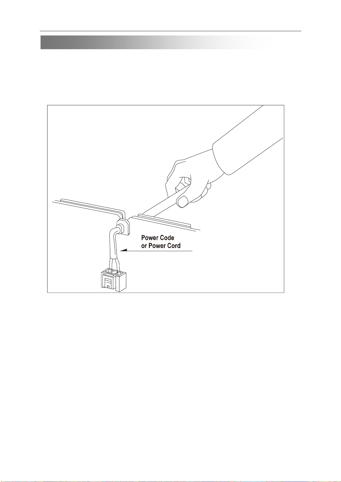
7. 1)When a power cord has been replaced ,check that A mark is made on the cord ,under strain ,near the
aperture ,and the flexible cord is subjected 100times to a pull of 40N for a duration of 1 second each .
2)During the test ,the cord shall not be displaced by more than 2mm
8.Also check areas surrounding repaired locations .
9. The internal wiring is secured so as not to approach the heating parts and high voltage parts by its shape.
So, these wires must be restored to its former state.
10. After updated the hazardous live part or accessible part, if the clearance or creepage distance cann’t
accord with the safe request, then need adopt reinforced insulation method for ensure safety.
SAFETY CHECK AFTER SERVICING
Examine the area surrounding the repaired location for damage or deterioration. Observe that screws ,parts
and wires have been reterned to original positions .
Afterwards ,perform the following tests and confirm the specified values in order to verify compliance wit
atfety standards .
2-2
Page 9
SAFETY PRECAUTIONS
·Insulation resistance test
confirm the specified insulation resistance or greater between power cord plug prongs and externally
exposed parts of the set (RF terminals ,antenna terminals ,video and audio input and output
terminals ,microphone jacks ,earphone jacks ,etc .)See table below.
·Dielectric strength test
Confirm specified dielectric strength or greater between power cord prongs and exposed accessible parts of
the set (RF terminals ,antenna terminals ,video and audio input and output terminals ,microphone
jacks ,earphone jacks ,etc.)See table below .
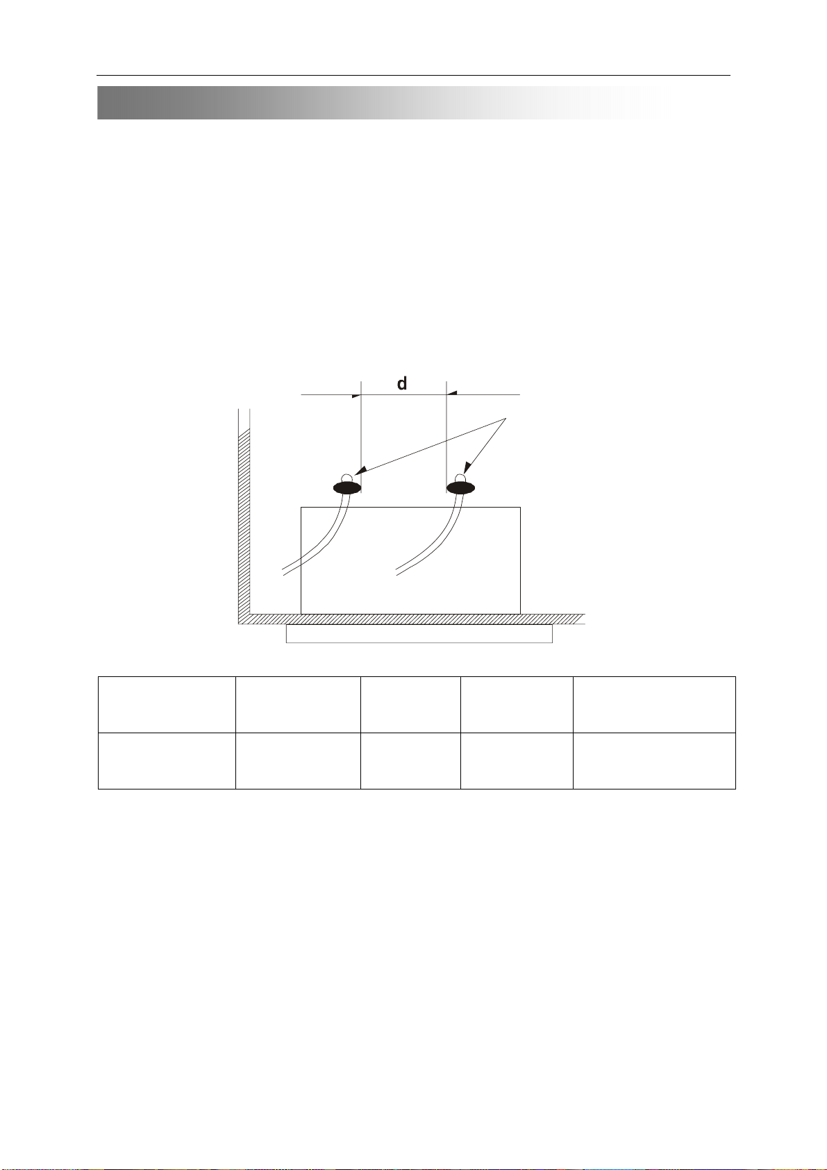
·Clearance distance
When replacing primary circuit components ,confirm specified clearance distance (d),between soldered
terminals ,and between terminals and surrounding metallic parts .See table below.
Table 1: Ratings for selected areas
Insulation
AC Line Voltage Region
*110 to 240 v
110 to 230 v
*Class ll model only .
Note . This table is unofficial and for reference only . Be sure to confirm the precise values for your
particular country and locality.
USA,Australia
Europe
Resistance
F
4M/500VDC
Dielectric
Steength
4kv/minute F 6mm(d)
Clearance
Distance(d),(d)
· Leakage Current test
Confirm specified or lower leakage current between B(earth ground ,power cord plug prongs ) and
externally exposed accessible (RF terminals ,antenna terminals ,video and audio input and output
terminals ,microphone jacks ,earphone jacks ,etc .)
2-3
Page 10
m
SAFETY PRECAUTIONS
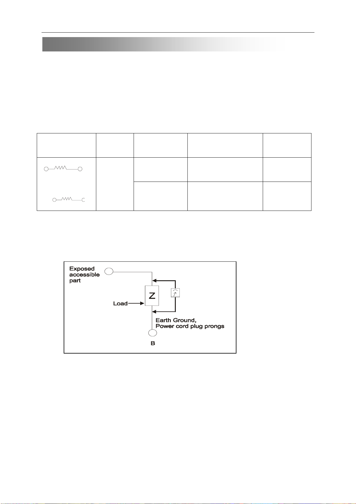
Measuring Method: (Power ON)
Insert load Z between B (earth ground ,power cord plug prongs )and exposed accessible parts .Use an AC
voltmeter to measure across both terminals of load Z . See figure and following table .
Table 2: Leakage current ratings for selected areas .
AC Line Voltage
2k ohm
100 to 130 v
200 to 240 v
50k oh
Note . This table is for IEC member only . Be sure to confirm the precise values for your particular country
and locality.
Region Load Z Leakage Current(i)
<or= 0.7mA peak
Europe
Australia
<or= 2mA DC
<or=0.7mA peak
<or= 2mA DC
Earth Ground
(B) to :
Antenna earth
Terminals
Other terminals
2-4
Page 11

Software Upgrade
MTK disc Upgrade Notice
1. The upgrading software must be recorded (burned) on a CD-R or CD-RW disc, and
a) Volume ID of the disc must be “MEDIATEK”, in capital letters. All Recording (burning)
software supports volume edit.
b) The upgrading software must be renamed as “MTK.BIN”, also in capital letters. You can rename
it on PC before recording.
c) The upgrading software MTK.BIN must be in root directory. Recording mode must be ISO9660
(MODE1, LEVEL1), DO NOT SELECT JOLIET, LOOSEN ISOSTRICT.
2. Load the disc
3. DVD will read disc, and prompt upgrading. Press “PLAY” on remote to confirm upgrading.
Note: Do not turn off the player while under upgrading; do not let electricity cut off. Otherwise the player
will halt and never be operate again.
If the DVD player cannot read the disc, please record some data file (trash files that the player cannot
support) before recording upgrading software.
3-1
Page 12
A
A
A
0
Electrical Performance Standards
No. Test item Requirement
1
2 Audio amplitude/frequency response (dB)
3
4
5
6 Cross-Sound base wave (dB) ≥80
7 1KHz Channel Balance (dB)
8 Intermodulation Distortion (dB)
9 Frequency error (dB) ±0.02
10
11
12
13
14 Output Intensity (iput 1KHz 20mVp-p)
15 Distortion and Noise (%)
16 Frequency Response (dB)
nalog output level(V) (Virtual value) 1.0~2.0v
20Hz ±1
125Hz ±1
1KHz ±1
10KHz ±1
18KHz ±1
20KHz ±1
udio SNR (dB) (A) ≥90
udio distortion and noise (dB) (1KHz) ≤-65
Dynamic Range (dB) (1KHz)
0
AUDIO FEATURE
Level non-linear (dB)
Digital out level (V) (Vp-p)
De-bass function (dB)
disc 784
DTS Test DOLBY Test
MIC
-10
-20
-40
-60
12 12 -4.53±1
13 13 -9.04±1
DTS
DOLBY
FL
FR
C
SL
SR
SW
120Hz ±3
5KHz ±3
dB 1KHz
output Level
Reference Level
≥80
≤1
≤-50
±1
0.5±0.05
Amplitude Response
under 0dB output
level (dB)
(20Hz-20KHz)
Reference Level
Amplitude Response
+0.5/-1.0(dB)
(20Hz-20KHz)
2.5±0.5V
≤0.5
17
18
19
20
Frequency error (dB)
Short Read Time (Sec)
other
Long Read Time (Sec)
Max Power Consumption (W)
≥45
≤5
≤10
15
4-1
Page 13
Electrical Performance Standards
No.
21
22
23
24
25
26
27
28
29
30
31
32
33
34
35
36
37
38
39
40
VIDEO FEATURE
Test item Requirement
Video Output Level
Vp-p(V)
Horizontal Definition (TV)
S video output
CVBS
FEAT
URE
Y, U , V
FEAT
URE
Luminance channel bandwidth
and Amplitude Response
(MHz)
Chroma channel bandwidth
and amplitude response (MHz)
Luminance non-linear distortion (%) ≤5
Luminance Wave distortion (%) ≤10
Luminance SNR (dB) ≥50
Chroma SNR (dB) AM≥60 PM≥50
Luminance/Chroma signal delay (ns) ≤100
Differential plus DG (%) ≤5
Differential Phase DP (°) ≤5
S-video signal amplitude Vp-p
load (mV)
S-video signal bandwidth and
amplitude response (MHz)
S-video signal SNR (Db)
YUV output signal amplitude
Vp-p load(mV)
YUV output signal bandwidth
and amplitude response (MHz)
YUV output signal SNR
(Db)
RGB output signal amplitude
Vp-p load(mV)
RGB output signal bandwidth
and amplitude response (MHz)
RGBoutput signal SNR
(Db)
CVBS output
Line Sync amplitude
VCD
AV output
VCD
SVCD
DVD
VCD
SVCD
DVD
Y channel 700±140
C channel
Y channel
C channel
Y channel
C channel
Y channel
U channel
V channel
Y channel
U channel
V channel
Y channel
U channel
V channel
R channel
G channel
B channel
R channel
G channel
B channel
R channel
G channel
B channel
Y channel
SVCD
DVD
VCD
SVCD
DVD
Chorma
Chroma
Sync
≥3.5-20dB
≥3.5-20dB
≥3.5-23dB
≥3.5-24dB
≥50
≥50
1.0±0.2
0.3±0.05
≥250
≥350
≥450
≥250
≥350
≥500
≥5.5-6dB
≥1.5-6dB
880±176
300±60
≥5.5-6dB
≥1.5-6dB
≥50
≥50
700±140
700±140
700±140
≥5.5-6dB
≥2-6dB
≥2-6dB
≥50
700±140
700±140
700±140
≥5.5-6dB
≥5.5-6dB
≥5.5-6dB
≥50
≥50
≥50
4-2
Page 14
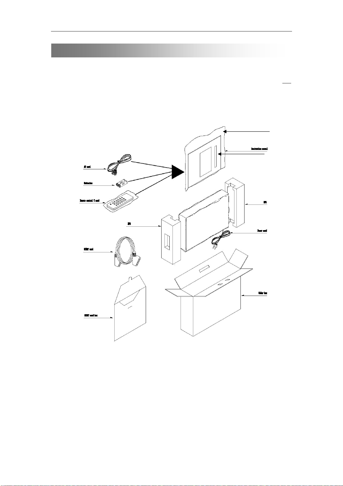
Package (Inbox)and Block Diagrams
1
2
6
7
3
4
5
8
9
10
1. AV Cable 6. Owner’s Manual bag
2. Batteries 7. Owner’s Manual
3. Remote control 8. EPS
4. scart Cable 9. Power cord
5. Scart cable box 10. Color box
5-1
Page 15
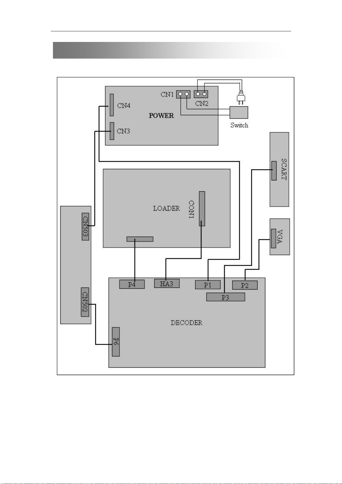
DVD Box Block Diagram
6-1
Page 16

General Classification of Symptoms
Common phenomenon classification
1.
Check Power line connect to
POWER?Check switch ?
Check signal wire connect to
decoder board correct?
2.
Check audio wire between
DVD player and TV
Check Scart wire
connection to TV
DVD audio setup correct?
To decoder board service D2\D3-1\D3-3
VFD no display
Y
Y
KB board OK?
N
To KB board service K1
TV no voice
Y
Y
Y
Y
N
Connect again. Normal?
N
Connect again, Normal?
T o decoder board service D1
N
N
N
Connect DVD left/right
channel to TV correctly
Connect again
Setup audio by referring to manual
7-1
Page 17

General Classification of Symptoms
3.
4.
Video wire connection correct? Connect to TV correctly
SCART wire connection correct?
Press “v.mode” key of the
REMOTE..
To decoder board service D3\D3-2\D3-3
Check Loader signal wire
connects to board correct?
Check flat ribbon connect to
decoder/servo board
TV no display
Y
Y
Y
Cannot open tray
Loader too low/high? Adjust loader
N
Y N
Y
N
N
N
Y
Connect again, TV display
normal?
N
Press times, normal?
N
N
Connect again, normal?
Connect again, normal?
N
7-2
Page 18

General Classification of Symptoms
5.
Check Loader wire connect to
decoder board correct
Check flat ribbon connect to
decoder board correct
Press “Open/Close” on front panel, the
data line of KB board has wave out?
Press “Open/Close” on remote control,
the IR line of KB board has wave out?
Do not read disc
Disc scratched/dirty? Replace disc
N
Y
Y
To decoder board service
Y
Y
To board service
Y
N
Connect again, normal?
N
N
Connect again, normal?
N
N
To KB board service K3
N
To KB board service K2
7-3
Page 19

General Classification of Symptoms
6.
7.
8.
Check optical/coaxial connection to
decoder device OK?
Image/voice distortion
Disc scratched/dirty? Replace
N
T o decoder board service D4, D5
Optical/Coaxial output abnormal
Audio setup correct? Adjust according to
Y
Y
T o decoder board service D6
Read disc and halt
Disc scratched/dirty? Replace/clean disc
N
To servo board service
Y
N
manual instruction
N
Adjust according to
manual instruction
Y
7-4
Page 20

General Classification of Symptoms
9.
10.
11.
12.
Reading drag To servo board service
control
MIC no voice To MIC service M1
To KB board service K3 Cannot operate by remote
To MIC service M2 MIC self activated
Judgment standard for loader damage
When below phenomenon exist, the loader may be damaged.
1. no spin
2. no laser
3. cannot open/close tray normally
4. main axis turning, but no pickup focus or gliding
5. cannot read discs
When above phenomenon exists, please try replacing loader to solve the
problem.
7-5
Page 21

8-1 Power Board Block Diagram
8-1
Page 22

8-1 Power Board Block Diagram
A
REV:
2005/09/06
Viper22+EE25
AKAI A-5181
DATE:
Title:
-12V
100UF/25V
E206
10UH
L201
E205
100UF/25V
D201
FR154
T101
103/1KV
C101
R101
D103
22U/400V
1N4007
D105
56K/2W
E101
D104
1N4007
+12V
E204
220UF/16V
10UH
L202
E203
220UF/16V
FR154
D202
FR107
磁珠
L102
65
IC101
5V
E202
1000UF/10V
10UH/2A
L203
E201
1000UF/10V
D204
IN5822
3
4
8
1
7
2
DH321 DIP
470/1/4W
R103
D106 FR104
R102
10R/1/4W
R201
4.7K/1/4W
R203
R203
C103
104/50V
2.2K/1/4W
C202
1K/1/4W
1
2
IC102
3
4
R202
4.7K/1/4w
104/50V
1
2 3
IC201
TL431
PC817
2200pF-250V
CY103
4.3V
ZD1
D101
1N4007
NF1
12mH
F101
T1AL 250V
1
2
CN101
D102
1N4007
L101
CX101
0.1uF-275V
1
2
8MM-2P
8MM -2P
CN102
E102
47UF/50V
8-2
Page 23

8
Main point waveforms and schematic diagrams of electronic components
8-1 Reference waveform of key test point of power board
TP1+12V (no disc) 3-mVpp TP1 (reading disc) 250mVpp
TP2+5V (no disc) 3-mVpp TP2+5V (reading disc) 40mVpp
TP3 (idle) 20Vpp TP3 (no disc)20Vpp
TP3 (reading disc)20Vpp
8-3
Page 24

8
Repair of Power Board
I. Power switch working principles
TinySwitch-II(TNY267) maintains the simplicity of the TinySwitchtopology, while
providing a number of new enhancements tofurther reduce system cost and component count,
and topractically eliminate audible noise. Like TinySwitch, a 700 Vpower MOSFET,
oscillator, high voltage switched current source,current limit and thermal shutdown circuitry
are integrated onto amonolithic device. The start-up and operating power are derived directly
from the voltage on the DRAIN pin, eliminating the need for a bias winding and associated
circuitry. In addition, the TinySwitch-II devices incorporate auto-restart, line undervoltage
sense, and frequency jittering. An innovative design minimizes audio frequency components
in the simple ON/OFF control scheme to practically eliminate audible noise with standard
taped/varnished transformer construction. The fully integrated auto-restart circuit safely lim its
output power during fault conditions such as output short circuit or open loop, reducing
component count and secondary feedback circuitry cost. An optional line sense resistor
externally programs a line under-voltage threshold, which eliminates power down glitches
caused by the slow discharge of input storage capacitors present in applications such as
standby supplies. The operating frequency of 132 kHz is jittered to significantly reduce both
the quasi-peak and average EMI, minimizing filtering cost.
1. Conversion from a.c. to d.c. circuit
220V a.c. current flows restrictively through F1 fuse, and through D301~D304 to
combine as bridge rectification. After C1L2C2 undergoes electrolytic filter, we can
obtain a 320V d.c. voltage (Uhv).
2. Process to start up the software
The TinySwitch-II does not require a bias winding to providepower to the chip, because
it draws the power directly from the DRAIN pin (see Functional Description above). This has
twomain benefits. First, for a nominal application, this eliminatesthe cost of a bias winding
and associated components.Secondly, for battery charger applications, the current-voltage
characteristic often allows the output voltage to fall close tozero volts while still delivering
power. This type of application normally requires a forward-bias winding which has many
more associated components. With TinySwitch-II, neither are necessary. For applications that
require a very low no-load power consumption (50 mW), a resistor from a bias winding to the
BYPASS pin can provide the power to the chip. The minimum recommended current supplied
is 750 µA. The BYPASS pin in this case will be clamped at 6.3 V. This method will eliminate
the power draw from the DRAIN pin, thereby reducing the no-load power consumption and
improving fullload efficiency. And check c5,it is very importance of starp up.
3. Bias winding
After starting the power, T P1~P2 bias winding supplies bias current and error current to
the internal of IC2 , through D7 and C4 rectifier filter and through R2 light-electric coupler.Check
IC2 BP pin (IC2 PIN1),it’s voltage is 6.3v.
8
8-4
Page 25

4. Regulation process of output voltage
When the input current of control pin (5) IC2 decreases (or increases), oscillation
waveform will be regulated automatically so that T ratio will increase (or decrease) and
the output voltage will increase (or decrease).
Output voltage feedback circuit is completed by Z1R8D13
5IC2 TNY267 introduction
8
8-5
Page 26

1No voltage output
Measure each output terminal to see
whether it is short circuit
NO
Measure the voltage ofC1L2C2
About 320V
YES
Far less than 320V
Eliminate short-circuit point
Check a.c. and d.c. conversion
elements such as FUSE, power
switch, D1D2D3D4 etc.
Measure the voltage of 5pin (VCC)
of IC2
About 320V
Measure whether the voltage of 1
pin IC (VFF) is equal to 2.8V
NO
0V
YES
Open circuit of 1~3 pins of T
PIC 817Z1 are damaged
Measure whether the voltage of 5
pin IC2 (5) is equal to 6.3V
NO
YES
Check whether C5R2D7C4R4
C6 are damaged
Test whether the windings of T are
short circuit, open circuit
NO
YES
Replace T
Measure other elements
8
8-6
Page 27

1. 2Unstable voltage output, decrease of carrier capability
Take out the output cord, connect
false loading
Abnormal
Normal output voltage
Measure the working temperature of
elements by infrared thermometer
Normal
Abnormal
Is the voltage of light-emitting tubes in
optical coupling at about 1V?
Yes
No
Is the reference voltage of R8 at
2.5V?
Yes No
No
Is the voltage of IC2 control pin
normal?
Yes
No
`
Is the voltage of C2at 320V?
No
+5V+12V-12V-24V is lower
Yes
Yes
Check other compents
No
Other power boards overloaded
Analyse heating elements
Replace optical coupling
Is it normal after replacing Z1?
Check D7R2
There is damage in D1D2D3D4,
forming half-wave rectification
Check D13R8Z1D12
8-7
Page 28

5
4
3
2
1
COMMON89D_KHM310_V5
MT1389D (LQFP216) DVD Demo Board for KHM310
1 INDEX & POWER, RESET
2 RF, SERVO & MPEG - MT1389E
D D
3 MEMORY - SDRAM, FLASH/EEPROM
4 VIDEO OUT
5 AUDIO DAC WMA8766
NAME
VCC
DV33
RFV33
LDO_AV33 Laser Diode 3.3V
AVCC
V18
SD33
+12V
-12V
+P5V
+P5V
AVDD
DVDD
VCC
VCC
L12
FB
C C
B B
A A
L7
FB
L9
FB
L5
FB
CB6
0.1uF
CB9
0.1uF
TYPE
Digital 5V
Digital 3.3V
Servo 3.3V
RF 5V
Digital 1.8V
Digital 3.3V
Audio +12V
Audio -12V
Audio 5V
Audio 3V3
CE3
CB4
+
220uF/16V
0.1uF
VCC_AUDIO
+
CE5
220uF/16V
AVCC
VCC
+
CE9
220uF/16V
+P5V
+P5V
+P12V
-P12V
A_MUTE
DEVICE
SUPPLY
MT1389E
MT1389E
PICKUP HEADER
MT1389E
SDRAM
OP AMP.
OP AMP.
Audio DAC
Audio DAC
+P5V
D20
1 2
1N4148
+P12V-P12V
V33
V33
6x1 W/HOUSING
L6
FB
L10
FB
L11
FB
J9
1
2
3
4
5
6
7
8
RFV33
LDO_AV33
CB5
0.1uF
+12V-12V
+
CE4
220uF/16V
CB7
0.1uF
CB8
0.1uF
+
+
CE7
220uF/16V
LDO_AV33
CE8
220uF/16V
RFV33
V33
V33
L2
FB
VCC
L4
NO_USER
Regulator
Fix regulator
Adj regulator
CB1
RT9164CG/AZ1117H-A DJ
U1
3
IN
GND
1
2
OUT
R1
300 1%
R2
680 1%
0.1uF
C1
+
CB2
0.1uF
CE2
220uF/16V
C
Power ON alive source
R1 R2
0 ohm
OFF
300 1% 680 1%
U2
RT9164 33/AZ1117 33
VCC V33
3
2
VI
VO
4
VO
GND
1
+
CE1
220uF/16V
L1
FB
L3
FB
DV33
DV33
V18
V18
CB3
0.1uF
A_MUTE
URST#
V18
DV33
VCC
AVCC
VCC_AUDIO
+12V
-12V
GND
DV33
A_MUTE [5]
URST# [ 2 ]
V18 [ 2 ]
DV33 [ 2,3,4,5 ]
VCC [ 2,3,4,5 ]
AVCC [ 2 ]
VCC_AUDIO [ 5 ]
+12V [ 4,5 ]
-12V [ 4,5 ]
GND [ 2,3,4,5 ]
D1
1N4148
R3
10k
CE6
+
10uF/16V
URST#
TP1
URST#
MediaTek Incorporation
Title
COMMON89D_KHM310_V5
Size Doc um e n t N u mb er Re v
C
5
4
3
2
Date: Sheet
INDEX
1
15Thursday, June 24, 2004
4
of
Page 29

5
L14
RFV33
R11
C14
680k
2200pF
R32 10k
R33 10k
R34 100k
AVCC
FB
+
Very Important to
reduce Noise
L20
10uH
Q4
2SB1132
1
3 2
R40 4.7
R41 4.7
Q5
32
2SB1132
1
VOTK+
VOTKVOLD+
VOLDPGND
VNFTK
PVCC2
G2
PREGND
VINLD
CTK2
CTK1
VINTK
BIAS
STBY
RFV33
ADIN
OP-
OP+
V1P4
AVCC
CE17
100uF/16v
1
R173
TP51
VOFC+
VOFC-
VOSL+
VOSL-
PGND
PVCC1
VCC
VNFFC
VOSL
VINSLVINSL+
CF2
CF1
VINFC
B
G1
CB13
0.1uF
TP12
TP13
TP14
TP15
TP16
IOA
2
C
C
E
2SB1132
10K
+
+
FF+
14
13
12
11
10
9
8
29
7
6
5
4
3
2
1
TP4
TP5
TP6
V2P8
+
3
CE18
47uF/16v
CE19
47uF/16v
LOAD+
LOAD-
L17
330uH
+
CE46
1000uF/16v
CE13
47uF/16v
C
B
A
D
RFO
C
B
A
D
RFVDD3
C37
C
CD
FB
ADACVDD3
CB14
0.1uF
C29 1uF
C31 1uF
C32 1uF
C34 C
TP18
TP19
TP20
TP21
TP22
TP23
TP24
TP25
TP26
TP27
TP28
TP29
TP37
R37
R
V18
R174
LDO2
LDO_AV33
LDO1
R45
1
SPSP+
TRCLOSE
TROPEN
FOSO
+
CE21
47uF/16v
CB17
0.1uF
100K
C19
6800PF
V20
+
CE14
47uF/16v
C30 1uF
R38
V18
C3 2200pF
R6 680k
R9
150k
SPSP+
LIMIT
SLSL+
DV33
R23 10k
V18
D
3
G
2
1
2SK3018
HA1
24
23
22
21
20
19
18
17
16
15
14
13
TOP
12
11
10
9
8
7
6
5
4
3
2
1
R43
1
TP52
TP54
MO_VCC
R15 R
R19 1
V18
S
LD-DVD
LD-CD
SL+
SL-
CB33
0.1uF
L18
FB
GND
AVCC1
MDI1
E
AVCC1
V20
GND
F
B
A
RFO
IOA
D
C
R44
1
R31 100k
2
Q2
R35
100
R59
10k
D D
C C
B B
HEADER 24 SMD0.5 TOP
A A
TP38
TP39
FMSO
TRSO
V1P4
STBY
OPO
CB16
0.1uF
13
R36
100
T-
R10
150k
1
2
3
4
5
6
6x1 W/HOUSING
RFV18
3
C
1
B
E
2N3904
2 3
13
2
Q3
CB18
0.1uF
L21
10uH
CB35
0.1uF
5
C4
0.1uF/N.C
R7 0
J1
2
1
Q1
L19
C38
0.1uF
TP50
U5
15
16
17
18
19
20
21
30
22
23
24
25
26
27
28
AM5668
R13
6.8
ADACVDD3
C33 1uF
SUBA
SUBB
SUBC
SUBD
E
F
MDI1
MDI2
LDO2
LDO1
TP32
TP33
TP34
C36
0.1uF
R
STBY
R46
1
TP53
TP55
MO_VCC
R54
20k
CB15
0.1uF
TP17
TP30
TP31
TP35
TP36
4
C5
0.1uF
+
CE12
100uF/16v
V1P4
+
CE15
47uF/16v
RFOP
RFON
V2P8
V20
V1P4
TEZISLV
OPO
OPOP+
DMO
FMO
TROPEN
TRO
FOO
ADIN
II_SDA
II_SCL
R39 0
A2
A3
A4
A5
A6
A8
A18
A19
DV33
FOSO
TRSO
FMSO
DMSO
DMSO
4
FEO
TEO
C6
0.01uF
C39
330pF
PLLVDD3
CB12
0.1uF
C40
330pF
RFVDD3
C7
2200pF
1
AGND
2
DVDA
3
DVDB
4
DVDC
5
DVDD
6
DVDRFIP
7
DVDRFIN
8
MA
9
MB
10
MC
11
MD
12
SA
13
SB
14
SC
15
SD
16
CDFON
17
CDFOP
18
TNI
19
TPI
20
MDI1
21
MDI2
22
LDO2
23
LDO1
24
SVDD3
25
CSO/RFOP
26
RFLVL/RFON
27
SGND
28
V2REFO
29
V20
30
VREFO
31
FEO
32
TEO
33
TEZISLV
34
OP_OUT
35
OP_INN
36
OP_INP
37
DMO
38
FMO
39
TROPENPWM
40
PWMOUT1/ADIN0
41
TRO
42
FOO
43
FG/ADIN1
44
GPIO0
45
GPIO1
46
GPIO2
47
IOA2
48
DVDD18
49
IOA3
50
IOA4
51
IOA5
52
IOA6
53
IOA7
54
HIGHA0
C41
0.1uF
VCC
C24
0.1uF
C42
L22
FB
R12 15k
C17 0 .1uF
RFVDD3
C20 0 .1uF
214
213
211
216
215
212
OSP
OSN
IREF
RFGC
AVDD3
IOA18
IOA19
DVSS
58
55
57
56
A16
PWR#
R47 20k
R48 18k
R49 15k
R50 10k
0.015uF
V1P4
MO_VCC
3
C12
1500pF
Y6
Y5
APLLVDD3
181
182
183
B
R
APLLVDD3
URD#
A0
RGB_SWITCH
UWR#
TP40
TP49
J4
1
2
3
4
5
5x1 W/HOUSING
JITFN
TP3
DACVDD3
CB11
0.1uF
TP9
TP8
ASDAT0
ASDAT1
ASDAT2
ASPDIF
ALRCK
174
CVBS
UP1_696DVSS
97
DACVSSC
SDA
173
172
FS
UP1_798UP3_099UP3_1
RESET#
TP47
DACVDD3
171
VREF
100
MUTE_DAC
TP43
FS0
169
164
167
166
165
163
168
170
SPDIF
ALRCK
DVDD3
ASDATA0
ASDATA3
ASDATA2
ASDATA1
MC_DATA
DACVDDC
UP3_4
101
102
RXD
TXD
ACLK
ABCK
DVSS
GPIO5
GPIO4
GPIO3
DVDD18
DVDD3
RA11
RCLK
DVSS
DVSS
RA10
DVDD3
RCS#
RAS#
DVDD18
CAS#
RWE#
DVSS
DQM1
RD10
RD11
RD12
DVDD3
RD13
RD14
DVSS
RD15
DVSS
DQM0
IR
UP3_5
GPIO7
ICE
PRST#
INT0#
DVDD3
U4
106
103
104
105
107
108
MT1389D
IR
INT0#
URST#
ICE
TRCLOSE
TP44
TP48
Y4
Y3
DACVDD3
DACVDD3
179
180
177
178
176
175
G
DACVSSA
DACVSSB
DACVDDA
DACVDDB
95
SCL
IOA
VSTB
VSDA
VSCK
R42
TP42
10k
DV33
JITFO
C2 39 0pF
TP2
10uF/10v
RFV18
192
XTALO
RFVDD18
C11
191
RFGND18
AL
190
189
ADACGND
AR
ADACVDD3
186
188
187
AL
AR
VCM
R5 750k
184
185
APLLVSS
APLLCAP
ADACVDD3
V1P4
C8 0.1uF
20pF
C9
R8 100k
1000pF
C16
RFVDD3
0.1uF
RFVDD3
C21 0. 03 3uF
C25
204
208
207
205
210
206
209
HRFZC
RFGND
CRTPLP
RFVDD3
ADCVSS
RFRPAC
RFRPDC
10uF/25v
C10
+
XI
XO
C13 0.47uF/N.C
C22 0.047uF
203
LPFOP
ADCVDD3
R17 0
C23 0.047uF
PLLVDD3
JITFO
JITFN
XTALI
201
194
195
202
198
193
200
199
196
197
JITFN
LPFIP
XTALI
JITFO
LPFIN
LPFON
PLLVSS
PLLVDD3
IDACEXLP
MT1389D
V1.7
HIGHA465HIGHA564HIGHA762DVDD361A1660IOWR#59DVDD3
HIGHA6
IOCS#
HIGHA366HIGHA1
IOA20
HIGHA2
A12
A13
DV33
68
69
67
A9
A20
A11
A10
FOO
TRO
FMO
DMO
R51 10k
R55 10k
71
70
A1
PRD#
PCE#
63
A14
A15
DVSS74IOOE#73IOA172DVSS
AD0
AD378AD4
76
75
79
AD2
AD4
AD1
AD3
AD0A7AD6
C45
0.1uF
3
AD681AD277AD1
ALE
IOA21
AD5
DVDD1884AD785A1786DVDD387IOA088UWR#89URD#90UP1_291UP1_392GPIO693UP1_494UP1_5
83
82
80
AD7
AD5
A21
ALE
A17
V18
TP41
TP45
LOADLOAD+
TROUT
TRIN
TP46
2
DV33
L15
FB
+
CE11
10uF/25v
DV33
FS
VREF
TP11
R24
4.7k
V18
162
161
160
159
158
157
156
155
RA4
154
RA5
153
RA6
152
RA7
151
150
RA8
149
RA9
148
147
CKE
146
145
144
RA3
143
142
RA2
141
RA1
140
RA0
139
138
137
BA1
136
BA0
135
134
133
132
131
130
129
128
RD8
127
RD9
126
125
124
123
122
121
120
119
118
RD0
117
RD1
116
RD2
115
114
RD3
113
RD4
112
RD5
111
RD6
110
RD7
109
DV33
1
RxD
2
TxD
3
4
4x1 W/HOUSING
ACLK
ABCK
MA4
MA5
MA6
MA7
MA8
MA9
MA11
DCKE
DCLK
MA3
MA2
MA1
MA0
MA10
BA1
BA0
CS#
RAS#
CAS#
WE#
DQM1
DQ8
DQ9
DQ10
DQ11
DQ12
DQ13
DQ14
DQ15
DQ0
DQ1
DQ2
DQ3
DQ4
DQ5
DQ6
DQ7
DQM0
J3
C28
0.1uF
C15
1000pF
L16 2.7u, DIP
XI
TP10
R22
2K
R25 0
R26 0
R27 0
CB24
0.1uF
ALRCK
R20
CB19
0.1uF
CB25
0.1uF
NC
TROUT
TRIN
LIMIT
C26
27pF
R29
1k
CB20
0.1uF
CB26
0.1uF
CB30
0.1uF
IR
147
U3A
1 2
74HC04
R16 100k
Y1 C27MHz
1 2
C35
100pF
CB21
CB22
0.1uF
0.1uF
CB28
CB27
0.1uF
0.1uF
CB31
0.1uF
R30 10
V18
DV33
DV33
DV33
CB23
0.1uF
CB29
0.1uF
CB32
0.1uF
C27
27pF
1
APLLVDD3
147
3 4
R21
NC
MUTE_DAC
MUTE_DACV1P4
URST#
A[0..21]
AD[0..7]
PRD#
PWR#
PCE#
MA[0..11]
DQ[0..15]
BA[0..1]
DQM[0..1]
DCLK
DCKE
CAS#
RAS#
WE#
CS#
ASDAT[0..2]
AL
AR
CB10
0.1uF
U3B
74HC04
XO
CE16
100uF/16V
CD
VSDA
II_SDA
VSCK
VSTB
II_SCL
RESET#
RGB_SWITCH
AVCC
PCE#
PWR#
Y[3..6]
FS0
VIDEO INTERFACE
FLASH
MEMORY
SCL
SDA
VSCK
VSDA
ALRCK
ACLK
ABCK
ASPDIF
AUDIO INTERFACE
R4
0
+
CE10
10uF/25v
R14 0
VCC
R28
10
+
R167
R168
R170
4.7K
4.7K
RESET# [5]
RGB_SWITCH [5]
AVC C [1 ]
PCE# [3]
PWR# [3]
MUTE_DAC [5]
MUTE_DAC [5]
URST# [1]
Y[3..6] [ 5 ]
FS0 [4]
A[0..21] [3]
AD[0..7] [3]
PRD # [3]
PWR# [3]
PCE# [3]
MA[0..11] [3]
DQ[0..15] [3]
BA[0..1] [3]
DQM[0..1] [3]
DCLK [3]
DCKE [3]
CAS# [3]
RAS# [3]
WE# [3]
CS# [3]
SCL [3]
SDA [3]
IIC
ASDAT[0..2] [5]
AL [5]
AR [5]
VSCK
VSDA
ALRCK [5]
ACLK [5]
ABCK [5]
ASPDIF [4]
L13
FB
XTALI
C18
C
J2
1
2
3
4
5
6
7
8
6x1 W/HOUSING
4.7K
DV33
RS-232
MediaTek Incorporation
Title
COMMON89D_KHM310_V5
Size Doc um e n t N u mb er Re v
C
2
Date: Sheet
RF&MEPG
1
25Thursday, June 24, 2004
4
of
Page 30

5
U7
MA0
21
MA1
MA3
MA4
MA5
MA6
MA7
MA0
MA1
MA2
MA3
MA4
MA5
MA6
MA7
MA8
MA9
MA10
MA11
DBA0
DBA1
SDCLK
SDCKE
DCS#
DRAS#
DCAS#
DWE#
DQM0
DQM1
MA8
MA9
MA10
DBA0
SDCLK
SDCKE
DCS#
DRAS#
DCAS#
DWE#
DQM0
DQM1
D D
C C
B B
A A
A0
22
A1
23
A2
24
A3
27
A4
28
A5
29
A6
30
A7
31
A8
32
A9
20
A10
19
BA/A11
35
CLK
34
CKE
18
CS
17
RAS
16
CAS
15
WE
14
DQML
36
DQMH
33
NC
37
NC
26
VSS
50
VSS
ESMT M12L16161A-7
TSOP50
U9
23
A0
24
A1
25
A2
26
A3
29
A4
30
A5
31
A6
32
A7
33
A8
34
A9
22
A10/AP
35
A11
20
BA0/A13
21
BA1/A12
38
CLK
37
CKE
19
CS
18
RAS
17
CAS
16
WE
15
DQML
39
DQMH
36
NC
40
NC
54
VSS
41
VSS
28
VSS
ESMT M12L64164A/N.C
TSOP54
5
DQ0
DQ1
DQ2
DQ3
DQ4
DQ5
DQ6
DQ7
DQ8
DQ9
DQ10
DQ11
DQ12
DQ13
DQ14
DQ15
VCC
VCC
VCCQ
VCCQ
VCCQ
VCCQ
VSSQ
VSSQ
VSSQ
VSSQ
DQ0
DQ1
DQ2
DQ3
DQ4
DQ5
DQ6
DQ7
DQ8
DQ9
DQ10
DQ11
DQ12
DQ13
DQ14
DQ15
VCC
VCC
VCC
VCCQ
VCCQ
VCCQ
VCCQ
VSSQ
VSSQ
VSSQ
VSSQ
DQ7
2
DQ6
3
DQ5MA2
5
DQ4
6
DQ3
8
DQ2
9
DQ1
11
DQ0
12
DQ8
39
DQ9
40
DQ10
42
DQ11
43
DQ12
45
DQ13
46
DQ14
48
DQ15
49
SD33
1
25
SD33
7
13
38
44
4
10
41
47
DQ7
2
DQ6
4
DQ5
5
DQ4
7
DQ3
8
DQ2
10
DQ1
11
DQ0
13
DQ8
42
DQ9
44
DQ10
45
DQ11
47
DQ12
48
DQ13
50
DQ14
51
DQ15
53
SD33
1
14
27
SD33
3
9
43
49
6
12
46
52
FLASH_VCC
R70
10k
R0603
FLASH_VCC
4
MA0
MA1
MA2 DQ2
MA3
MA4
MA5
MA6
MA7
MA8
MA9
MA10
DBA0
SDCKE
DBA1
DRAS#
DCAS#
DWE#
DQM0
DQM1
A1
A2
A3
A4
A5
A6
A7
A8
A9
A10
A11
A12
A13
A14
A15
A16
A17
A18
A19
AA20
AA21
PCE#
PRD#
PWR#
TSOP48
U8
21
A0
22
A1
23
A2
24
A3
27
A4
28
A5
29
A6
30
A7
31
A8
32
A9
20
A10
19
BA/A11
35
CLK
34
CKE
18
CS
17
RAS
16
CAS
15
WE
14
DQML
36
DQMH
33
NC
37
NC
26
VSS
50
VSS
ESMT M12L16161A-7
TSOP50
A20 AA20
25
24
23
22
21
20
19
18
48
17
16
10
26
28
11
12
16Mb
R61 R
R62 R
32Mb
U11
A0
A1
A2
A3
A4
A5
A6
A7
8
A8
7
A9
6
A10
5
A11
4
A12
3
A13
2
A14
1
A15
A16
WP/ACC
A17
A18
9
A19
A20
CE
OE
WE
RESET
STM29W160/MX29LV800(160)
TSOP 48 pin
8M 16M 32M FLASH
4
D10
D11
D12
D13
D14
D15
BYTE
VCC
GND1
GND2
R0603
R0603
D0
D1
D2
D3
D4
D5
D6
D7
D8
D9
2
DQ0
3
DQ1
5
DQ2
6
DQ3
8
DQ4
9
DQ5
11
DQ6
12
DQ7
39
DQ8
40
DQ9
42
DQ10
43
DQ11
45
DQ12
46
DQ13
48
DQ14
49
DQ15
1
VCC
25
VCC
7
VCCQ
13
VCCQ
38
VCCQ
44
VCCQ
4
VSSQ
10
VSSQ
41
VSSQ
47
VSSQ
AA21A21
29
31
33
35
38
40
42
44
30
32
34
36
39
41
43
45
R67 10k
14
47
37
27
46
AD0
AD1
AD2
AD3
AD4
AD5
AD6
AD7
A0
DQ0
DQ1
DQ3
DQ4
DQ5
DQ6
DQ7
DQ8
DQ9
DQ10
DQ11
DQ12
DQ13SDCLK
DQ14
DQ15
SD33
SD33
CB53
0.1uF
C0603
R0603
FLASH_VCC
CB54
0.1uF
C0603
3
CB38
CB37
FB3MM
NO_USE
NC
FB3MM
RESET
Vcc
IO0
IO1
IO2
IO3
IO4
IO5
IO6
IO7
IO8
IO9
IO10
IO11
IO12
IO13
IO14
IO15
BYTE
GND
GND
CB50
0.1uF
C0603
CB36
CB44
0.1uF
C0603
SD33
CB51
0.1uF
C0603
0.1uF
C0603
23
15
17
19
21
24
26
28
30
16
18
20
22
25
27
29
31
44
33
13
32
0.1uF
C0603
CB49
0.1uF
C0603
SD33
CE24
+
47uF/16V
DC10A
FLASH_VCC
CE25
+
47uF/16V
DC10A
FLASH_VCC
AD0
AD1
AD2
AD3
AD4
AD5
AD6
AD7
A0
FLASH_VCC
0.1uF
C0603
CB45
0.1uF
C0603
CE22
+
220uF/16V
DC100A
CE23
+
220uF/16V
DC100A
DV33
L23 FB
VCC
L24
DV33
L25 FB
TS48
11
10
9
8
7
6
5
4
42
41
40
39
38
37
36
35
34
3
2
43
14
12
U10
A0
A1
A2
A3
A4
A5
A6
A7
A8
A9
A10
A11
A12
A13
A14
A15
A16
A17
A18
WE
OE
CE
AT49F8192A, SOP
8M Flash
A1
A2
A3
A4
A5
A6
A7
A8
A9
A10
A11
A12
A13
A14
A15
A16
A17
A18
A19
PWR#
PRD#
PCE#
3
2
SD33
CB39
CB40
0.1uF
0.1uF
C0603
C0603
SD33
CB46
CB47
0.1uF
0.1uF
C0603
C0603
DCS#
DRAS#
DCAS#
DWE# WE#
DBA0
DBA1
SDCKE
SDCLK
2
CB42
CB41
0.1uF
0.1uF
C0603
C0603
CB48
0.1uF
C0603
RN1
1 2
3 4
5 6
7 8
R63 33
R64 33
R65 33
R66 33
Title
Size Document Number Rev
Date: Sheet
CB43
0.1uF
C0603
[ 2 ]
[ 2 ]
[ 2 ]
[ 2 ]
[ 2 ]
[ 2 ]
CS#
33x4
RN-8
R0603
R0603
R0603
R0603
RAS#
CAS#
BA0
BA1
DCKE
DCLK
DV33
CB52
0.1uF
C0603
[ 2 ]
GND
DV33
VCC
U12
1
NC
2
NC
3
NC
GND4SDA
EEPROM 24C16
SOP8
MediaTek Incorporation
COMMON89D_KHM310_V5
B
SDRAM&FLASH
DQ[0..15][ 2 ]
MA[0..11][ 2 ]
BA[0..1]
DQM[0..1][ 2 ]
DCLK
DCKE
CAS#
RAS#
WE#
CS#[ 2 ]
PCE#
PRD#[ 2 ]
PWR#[ 2 ]
A[0..21][ 2 ]
AD[0..7][ 2 ]
SCL[ 2 ]
SDA[ 2 ]
VCC
SCL
1
WP
1
DQ[0..15]
MA[0..11]
BA[0..1]
DQM[0..1]
DCLK
DCKE
CAS#
RAS#
WE#
CS#
DRAM
PCE#
PRD#
PWR#
A[0..21]
AD[0..7]
FLASH
SCL
SDA
IIC
GND [ 1,2,3,4,5 ]
DV33
[ 1 ]
VCC
[ 1 ]
R68
680
R0603
8
7
6
5
of
35Thursday, June 24, 2004
R69
680
R0603
DV33
SCL
SDA
4
Page 31

5
R172
75,1%
NC
D D
Y3
R73
C C
3906
C
B
B B
A A
39,1%
E
Y3
R78
150,1%
Y4
R81
150,1%
Y5
R91
150,1%
5
L33 1.8uH, DIP
C72
47P
1.8uH,DIP
L26
C46
47P
L27 1.8uH,DIP
C48
47P
L28 1.8uH ,DIP
C50
47P
L31 1.8uH,DIP
C52
47P
R171
C73
47P
R71
75,1%
NC
R72
C47
47P
R76
75,1%
NC
R77
C49
47P
R79
75,1%
NC
R80
C51
47P
R83
75,1%
NC
R87
C53
47P
Q25
3906
+5VV
Q6
3906
+5VV +5VV
Q7
3906
+5VV
Q8
3906
+5VV +5VV
Q10
3906
+5VV+5VV
+5VV
1 2
1 2
+5VV
1 2
1 2
D2
1N4148
1 2
D3
1N4148
1 2
D4
1N4148
D5
1N4148
D6
1N4148
1 2
D7
1N4148
1 2
D8
1N4148
1 2
D9
1N4148
1 2
D18
1N4148
D19
1N4148
4
4
CVBS1
CVBS
CVBS_ST
G/Y
B/U SC
SCART CONNECTOR
SCART CONTROL
+12V
R84
680
R85
10k
VCC
R89
2.2k
RGB_SWITCH[ 2 ]
Y6
G/Y
ML
MR
CVBS_ST
ASPECT
RGB/CVBS#
R/V
B/U
Q27
2N3904
2 3
1
VCC
R100
150,1%
FS0[ 2 ]
FS1[ 2 ]
3
R53
300
R97
4.7K
3
L32 1.8uH,D IP
C54
47P
J5
1
2
3
4
5
6
7
8
9
10
SCART, 11P, PITCH=2.0M/M
FS1
Q26
8550
2 3
R52
1
10k
R57
1
2.2k
R93 0
R95
2 3
33
R99 2.2k
1
Pitch=2.0 m/m
R82 0
R85
1k
Q11
2N3904
2 3
Q14
8550
1
R96
75,1%
NC
R98
C55
47P
|
V
A21
C
B
E
3904 / 3906
R90
2.2k
CB56
0.1uf
+5VV
Q15
3906
1
RGB/CVBS#
2 3
ASPECT
R86
75
Q12
2N3904
+5VV
1 2
1 2
D10
1N4148
D11
1N4148
2
R/V SY
2
G/Y
B/U
R/V
YCbCr, 4P, PITCH=2.54M/M
J7
1
2
3
4
1
Y
Cr
Cb
CVBS
CVBS1
RESET#
MUTE_DAC
RGB_SWITCH
SC
VCC
Y[3..6]
AL
AR
ML
MR
G/Y
B/U
R/V
FS0
A21
ASDAT0
GND
VCC
+12V
-12V
1 2
3 4
VCC
L30
TO-92
R88
10k
R92 4.7k
RESET#
CVBS [5]
CVBS1 [5]
RESET# [2]
MUTE_DAC [5]
Y[3..6] [ 2 ]
AL [ 2 ]
AR [ 2 ]
ML [ 5 ]
MR [ 5 ]
G/Y
B/U
R/V
FS0 [ 2 ]
A21 [ 2 ]
ASDAT0 [ 2 ]
RGB_SWITCH [2]
GND
VCC [ 1 ]
+12V [ 1 ]
-12V
CY
GG
5
L29
NO_USER
Q9
FB
8550
2 3
1
Q13
1
2N3904
2 3
[ 5 ]
[ 5 ]
[ 5 ]
[ 1 ]
[ 1 ]
P1
S-VIDEO + RCA
+5VV
CB55
0.1uF
SY
CE26
+
47uF/16V
A2
MediaTek Incorporation
Title
COMMON89D_KHM310_V5
Size Docum ent Num ber Re v
Custom
Date: Sheet
VIDEO OUT PORT
1
45Thursday, June 24, 2004
of
4
Page 32

5
4
3
2
1
MIC_R
MIC_L
R138
180k
R153
180k
R164
180k
10uF/16V
CE32
10uF/16V
R123
180k
CE35
10uF/16V
R147
180k
CE41
10uF/16V
CE43
10uF/16V
10uF/16V
10uF/16V
R110
180k
CE48
+
+
+
CE38
+
10uF/16V
+
+
CE20
CE28
R74
+
68k
+
R111
100k
R75
68k
R119
10k
R124
100k
R135
10k
R139
100k
R143
10k
R148
100k
R150
10k
R154
100k
R160
10k
R165
100k
R105
10k
C59
2200pF
C61
2200pF
C65
2200pF
C69
2200pF
C57
2200pF
R136
5.1k
C63
2200pF
R151
5.1k
R149
20k
R114
20k
R120
5.1k
R130
R144
5.1k
R157
R161
5.1k
3
R101
20k
C56 220pF
-12V
R106
5.1k
U13A
-
2
1
+
3
NJM4558 OPA
8 4
+12V
Notice
When use internal Adac must change follow value
CE29
+
10uF/16V
R108
100
A_MUTE
ML
Q16
1
2N3904
2 3
R101&R114=31K;C57&C59=1000PF;C56&C58=100PF
C57
2200PF
C58
220PF
C59
2200PF
C56
R101
2 3
2 3
2 3
2 3
Q20
2N3904
Q21
2N3904
Q22
2N3904
2 3
Q23
2N3904
Q24
2N3904
31K
20K
MR
SL
SR
CENT
SUB
2
R114
31K 100PF 1000PF 100PFInternal DAC 1000PF
20K
220PF
C58 220pF
-12V
U13B
-
6
+
5
NJM4558 OPA
8 4
+12V
C60 220pF
20k
R141
20k
20k
-12V
-
2
+
3
8 4
+12V
C62 220pF
-
6
+
5
8 4
C64 220pF
-12V
-
2
+
3
8 4
+12V
C68 220pF
-12V
-
6
+
5
8 4
+12V
U14A
1
NJM4558 OPA
-12V
U14B
+12V
U16A
1
NJM4558 OPA
U16B
NJM4558 OPA
7
7
NJM4558 OPA
7
CE33
+
10uF/16V
CE36
+
10uF/16V
CE39
10uF/16V
CE42
+
10uF/16V
CE44
+
10uF/16V
+
CB65
0.1uF
+12V
CB61
0.1uF
External DAC
R121
100
A_MUTE
1
R137
100
A_MUTE
1
R146
100
A_MUTE
1
-12V
CB67
CB66
0.1uF
0.1uF
R152
100
A_MUTE
1
CB62
CB63
0.1uF
0.1uF
R162
100
A_MUTE
1
G/Y
B/U
R/V
[1] A_MUTE
[ 1 ]
[ 1 ]
[ 1 ]
[ 1,2,3,5 ]
[ 2 ]
[ 2 ]
[ 2 ]
[ 2 ]
ACLK
ALRCK
ABCK SBCLK
ASDAT0
ASDAT1
ASDAT2
CVBS1
1
CVBS
2
MR
4
ML
5
7
8
10
11
SR
SL
SUB
CENT
MR
ML
R58
10 0805
+12V
R60
10 0805
-12V
[ 4 ]
G/Y
B/U [ 4 ]
R/V
[ 4 ]
A_MUTE
[4] CVBS
[4] CVBS1
VCC_AUDIO[ 1 ]
ASPDIF
ASDAT[0..2][ 2 ]
ACLK
ABCK
ALRCK[ 2 ]
MUTE_DAC
ML[ 4 ]
MR[ 4 ]
P2
RCA-AV8
Title
Size Doc um e n t N u mb er Re v
C
Date: Sheet
CVBS
CVBS1
AL[2]
AR[2]
ASPDIF
ASDAT[0..2]
ACLK
ABCK
ALRCK
MUTE_DAC
ML
MR
J6
1
2
3
4
5
6
6PIN 2.0
J8
1
2
3
4
5
6
7
8
9
J10
1
2
3
4
5
6
6PIN 2.0
-12V
+12V
DV33
VCC
VCC_AUDIO
GND
SACLK
SLRCK
SDAT0
SDAT1
SDAT2
9PIN 2.0
3
6
9
12
-12V
+12V
DV33[ 1 ]
VCC
GND
AL
AR
R125 33
R126 33
R127 33
R131 33
R132 33
R133 33
MIC_L
MIC_R
MediaTek Incorporation
COMMON89D_KHM310_V5
AUDIO OUT PORT
1
of
55Thursday, June 24, 2004
4
+12V
VCC
R102
R103
R
0
D12 1N4148
1 2
D14
R107
22k
1N4148
R129
0
11
12
14
13
19
20
R116
100k
A_DVDD
5
6
1
2
3
4
7
8
9
1 2
R112 470
+
CE31
100uF/16V
23
Q19
1
8550
R166
560
VREFP Modify For WM87xx Series
U15
DVDD
AVDD
VFEFP
DGND
AGND
VREFN
MODE
ML/I2S
MC/IWL
VOUT1L
MUTE
VOUT1R
MD/DM
VOUT2L
VOUT2R
VOUT3L
MCLK
VOUT3R
BCLK
LRC
DIN1
DIN2
DIN3
NC
NC
WMA8766
VMID
TESTREF1
DNC
D D
VCC
R115
4.7k
MUTE_DAC
R118 10K
DV33
R128
R134
10,0805
R145 0
R
A_DVDD
CB57
A_AVDD
A_AVDD
CB58
0.1uF
R142 R
SACLK
SBCLK
SLRCK
SDAT0
SDAT1
SDAT2
0.1uF
+
CE34
100uF/16V
+
CE37
100uF/16V
A_DVDD
A_DVDD
VCC_AUDIO
C C
B B
HARDWARE:IIS 24BIT
CB68
ASPDIF
0.1uF
A A
5
R155
100
R163 22
C66
100pF
R156
75
OPTICAL
C70
27pF
C67
100pF
CB69
0.1uF
VCC
1
28
17
27
16
21
22
23
24
25
26
18
15
10
R159
22
23
Q17
8550
D15 1N4148
D17
+
A_AVDD
CB64
0.1uF
R158
110
CE45
+
10uF/16V
+
CE27
470uF/16V
1 2
1N4148
1 2
CE47
220uF/16v
CB59
DAC_ML
DAC_MR
DAC_SL
DAC_SR
DAC_CENT
DAC_LFE
+
10uF/16V
RCA
123
1
2
3
0.1uF
CE40
P4
P3
SPDIF
R122 100k
DAC_VREFP
C71
0.1uF
R140
CB60
0.1uF
4
R113 1k
330
A_MUTE
-12V
A_AVDD
DAC_ML
DAC_MR
-12V
DAC_SL
DAC_SR
DAC_CENT
DAC_LFE
Page 33

8
8-13
Page 34

8-14
Page 35

8-15
Page 36

MTK DECODER
MTK1389D decoder board service manual
Please check the power supply to decoder board is normal before checking
the decoder board.
Check the power supply voltage has the normal wave.
+5V+12V-12V3.3V(U2), 1.8V(U1)
Check reset circuit (reset at high electrical level)
Check crystal circuit (27MHz) and SDRAM frequency (108MHz)
Decoder board repair flow chart: (Diagram not included)
1.
VFD no output
Check P6 socket and plug connection bad Connect
good
Check CLK, DATA, STB wave out with check KB board
without
Check MT1389D PIN94,95,96 short circuit
short
Replace MT1389D
8-16
Page 37

MTK DECODER
2.
CVBS no output(audio/tray door normal)
Check the video cord connection bad connect correctly
good
Check video setup (software menu) bad Set to CVBS
yes good
Check Q7 emitter voltage between 1.0±0.2VPP
(use standard color band signal disc to test)
yes no
Check Q7 basal pole between 0.4±0.2VPP
no
remove Q7, check PCB Q7 base pole between
0.4±0.2VPP no replace Q7
no
Check MT1389D PIN175 output short circuit
yes
replace IC MT1389D
8-17
Page 38

t
MTK DECODER
3. YUV no output (Audio normal)
Check YUV port connected to TV correct bad
Correctly
Connect YUV
yes
Check video setup to YUV no set to YUV
yes
yes Check Q8, Q10, Q15 emitter voltage
between 0.7±0.14VPP
no
yes Check Q8Q10Q15 base pole voltage
between 0.1±0.14VPP
no
removeQ8, Q10, Q15, check Q8, Q10, Q15
base pole voltage between 0.1±0.14VPP
no
no
Check MT1389D PIN179181
182short circui
yes
Replace MT1389D IC
8-18
ReplaceQ8,Q10
Q15
Page 39

MTK DECODER
4.
VGA video no output (VGA contains R, G, B
signal and line/field sync signal. R, G, B signal
testing method is the same as YUV
Check VGA connect bad Connect correct
Good
Check DVD system (PAL/NTSC) is the same as TV setting. (In
VGA-PAL, line sync frequency is 31250Hz, field sync frequency is 50Hz.
In VGA-NTSC, line sync frequency is 31500Hz, field sync frequency is
60Hz
no yes
Set DVD PAL/NTSC Check MT1389D PIN 4445 short
circuit under normal frequency
no
Replace MT1389D
8-19
Page 40

MTK DECODER
5. SCART video no output
Refer to manual
no
In Scart-CVBS, “RGB-SWITCH” is
3.3V high, in RGB, it is 0V.
Check MT1389DPIN169
Check Scart port connect correct
Check DVD player is set to
SCART(CVBS/RGB
yes
bad
Check RGB signal, SCART sockets
PIN15, 11, 7. Method refer to YUV
In Scart-CVBS, PIN167 voltage should be
0-0.4V, in Scart-RGB, it should be 1-3VCheck
good
PIN167 voltage
SCART no audio output
Checking method refer to Left/Right
Channel, Check SCART sockets PIN2
PIN6
8-20
Page 41

MTK DECODER
p
s
wav
e 5 .6
V V
g
ght) with s
wave
5.6V V
s
wave
.6
V V
s
wave signa
s
wave signa
C
6.
No 5.1 channel
ut
out
No Left/Right
A B C
load 1K signal disc, check L37 (left
channel),L38 (right channel) with
in-
Replac
e U14
MUTE
Check “DAC-ML”,
yes
“DAC-MR” with
Check
in-
PP
l
No Surround
No Center,
No output
Check connection
ood
bad
Connection refer
to manual
load 1K signal disc, check L39
(surround left),L40 (surround
ri
in-
load 1K signal disc, check L41
(center), L42 (subwoofer) with
PP
no
Check “A-MUTE” signal is minus voltage
Replace
U14
yes
yes
Check “DAC-SL”,
“DAC-SR” with
in-
l
“DA
in-
“DAC-CETL”,
5
Check
-LFE” with
PP
yes
Replac
e U14
Check audio DAC, U12, WM8766 output
No KARAOKE output
Check Mic
board
Use signal generator to input 1KHz, 0.1VPP sin-wave, check
no
whether P1 port “MIL-L”, “MIC-R” has sin-wave signal
Check U14 circuit normal (Refer
to Left/Right channel Checking)
8-21
no
yes
Page 42

MTK DECODER
7.
Servo initial work process
Power On
System initiated, MT1389D reset and
initiated, wait for task
yes
Tray door close?
no
Close tray door
Pickup in inner circle?
no
Pickup move outward
yes
Machine initiatedMT1389D
Check disc
Without disc
With disc
Auto adjust
Wait for order
8-22
Page 43

MTK DECODER
Check disc
Activate pickup
Focus loop move up
Focus loop move down
no
Disc check error
yes
Focus loop move up
Focus loop move down
Pickup LD off
Initiate auto adjust
Action repeat
8-23
Page 44

MTK DECODER
8.
Check MT1389D
PIN39(TROPEN),
PIN103(TRCLOSE)
Check IC U3
Eject tray abnormal
(CVBS normal)
Check “TROPEN”, “TRCLOSE” signal level
normal (When open tray, “TROPEN” should be
high level, “TRCLOSE” should be low level
yes
Check “LOAD+”, “LOAD-“ voltage
no
larger than3.0V (connect multimeter black
pen to “LOAD-”, red pen to “LOAD+”
yes
Check “P4” or “P5” connection with loader
Close tray abnormal (CVBS normal)
Check MT1389D
PIN39(TROPEN),
PIN103(TRCLOSE)
Check IC U3
Check “TROPEN”, “TRCLOSE” signal level
no
normal (When open tray, “TROPEN” should be
low level, “TRCLOSE” should be high level
yes
Check “LOAD+”, “LOAD-“voltage larger
no
than3.0V (connect multimeter red pen to
“LOAD-”, black pen to “LOAD+”
Check “P4” or “P5” connection
8-24
Page 45

8 Repair of key board
8-25
Page 46

8 Repair of key board
8-26
Page 47

b
board connectio
SM169
Repair of key board
KB BOARD SERVICE PROCEDURE
Check other components
Power on
LED HAS
DISPLAY?
Check Power
oard and KB
Check KB board
input power
normal
Check IC
4
LED work
properly?
YES
NO
YES
n
good
YES
OK
bad
Connect
correctly
NO
Make Power board
under normal supply
YES
Replace IC
NO
Replace LED
8-27
Page 48

Repair of MIC board
6PIN/2.5
-12V
6
+12V
5
4
MIC1
3
GND
2
MIC2
1
PHO401
CN401
C401
3300pF
L401
3.3uH
C407 0.1uF
E403 100uF/16V
R401
1k
C402
3300pF
C403
0.1uF
R403
22k
12
+12V
84
3
+
2
-
-12V
R407 51k
C404 680pF
R405
2k
5
6
C405 100pF
R406
2k
U401A
4558
+12V
84
+
-
-12V
R408 10k
1
U401B
4558
7
C406 0.1uF
12
E402 100uF/16V
R409
10
R410
10k
R-VAR1
3
vr401
3
6
6
2
5
2
5
4
4
1
1
R417
10
E401
1 2
10uF/16V
E404
10uF/16V
12
8-28
Page 49

b
Repair of MIC board
MIC BOARD SERVICE PROCEDURE
NO MIC
Microphone
normal?
MIC signal wire
connects to
Volu me
potentiometer
MIC board power
When MIC has
input, IC 4558 Pin
Check decoder
oard
NO
NO
NO
NO
NO
NO
NO
NO
NO
NO
NO
NO
Replace microphone,
return normal?
Connect correct, return
normal?
Replace potentiometer,
return normal?
Check Power board and
Mic board connecting
wires
Replace IC4558, return
normal?
8-29
Page 50

9-1
 Loading...