

Page 1

DVD PLAYER
Model:
A1211
SERVICE MANUAL
www.akai.ru
Page 2

1. CONTENTS
DVD Service Manual
Title
1. CONTERTS
2. BLOCK DIAGRAM (CABLE CONNECTIONS)
3. POWER SUPPLY
4. FUNCTIONAL DESCRITPIONS
4.1 DVD MPEG board
4.2 Front Panel
4.3 SMPS
4.4 DVD Driver
5. DESCRIPTION OF THE INTEGRATED
CIRCUITS
5.1 SWPS TRANSFORMER
5.2 SWPS CONTROLLER IC (TEA1523P)
Page
1
2
3
4
4
14
15
16
18
18
19
5.3 SWPS PROGAMMABLE SHUNT RE
GULATOR (FAIRCHILD TL 431)
5.4 LINE FILTER(2 x 25mH)
6. FAULT TRACING FLOW CHART
6.1 POWER SUPPLY
6.2 FRONT PANEL
6.3 MPEG BOARD
7. COMPONENT LIST
21
22
23
23
24
25
26
1
Page 3
DVD Service Manual
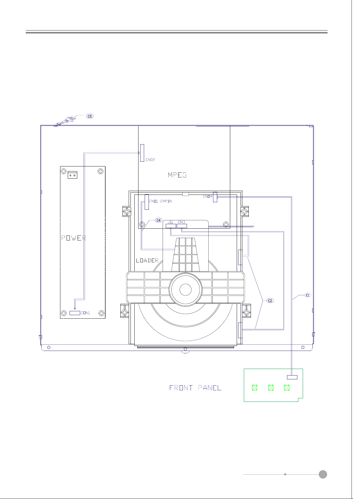
2. BLOCK DIAGRAM (CABLE CONNECTIONS)
2
Page 4
DVD Service Manual
3. POWER SUPPLY
D
12345
JP2
F2F1-21V
4321
3.8V/0.2A
F2
R11
2.2k
R9
470
R10
470
D5V
0.1A
F1
-21V
D9
9.1V
C13
0.1u/50V
C
12345
Jp4
-12V
+12V
D5V
1.8A
1.2A
-12V
100mA
C15
0.1u/50V
R14
1K
+12V
C18
0.1u/50V
CE11
220u/25V
R16
B
6
D5V
D5V
270
C21
C20
A
1/1
V1.1
Number RevisionSize
A4
Title
0.1u/50V
0.1u/50V
Date: Sheet of
File: Drawn By:
CE9
10u/50V
CE7
10u/50V
L4
CE3
470u/10V
D4
FR102
T1
NC
C7
C6
20uH
L3
C10
470p/1KV
FR102
D5
11
12
10
1
47K
R2
2.2n/AC400V
IN4007
4
IN4007
RT1
NTC10D-11
D
20uH
D6
FR102
CE6
100u/50V
13
14
5
D1
HER157
10n/630V
C5
CE2
22u/50V
47u/400V
CE
IN4007
IN4007
C4
C3
34
L1
C2
0.22/275VAC
L5
20uH
CE10
1000u/25V
CE8
100u/25V
D7
HER207
C17
471/1KV
C14
470p/1KV
15
18
15
16
14
8
9
FB1
ER102
D2
HGND
471/275VAC
IC1
R1233
471/275VAC
12
C24
104
0.22/275v
C1
VR1
S07K275
FUSE
C
L6
20uH
D8
SB360
R5
75K
6NC7
8
DRAN
SOURCE
VCC1GND2RC3REG
6.8K
R7
T630mA220VAC
CE14
CE13
2200u/10V
470u/10V
R17
2.2K
R15
22
C19
102/1KV
R4
5
AUX
4
R8
C16 680P
SW1
HGND
0.47
TEA1523
104P
2.2K
C23
HGND
1
2
CN1
220VAC
B
330
R33
CE15
10u/25V
IC2
4.7K
R6
C22
R18
R20
680
R19
1K
PC817
R21
2.2K
104/50V
1K
IC3
TL431C
1 2 3 4
A
3
Page 5
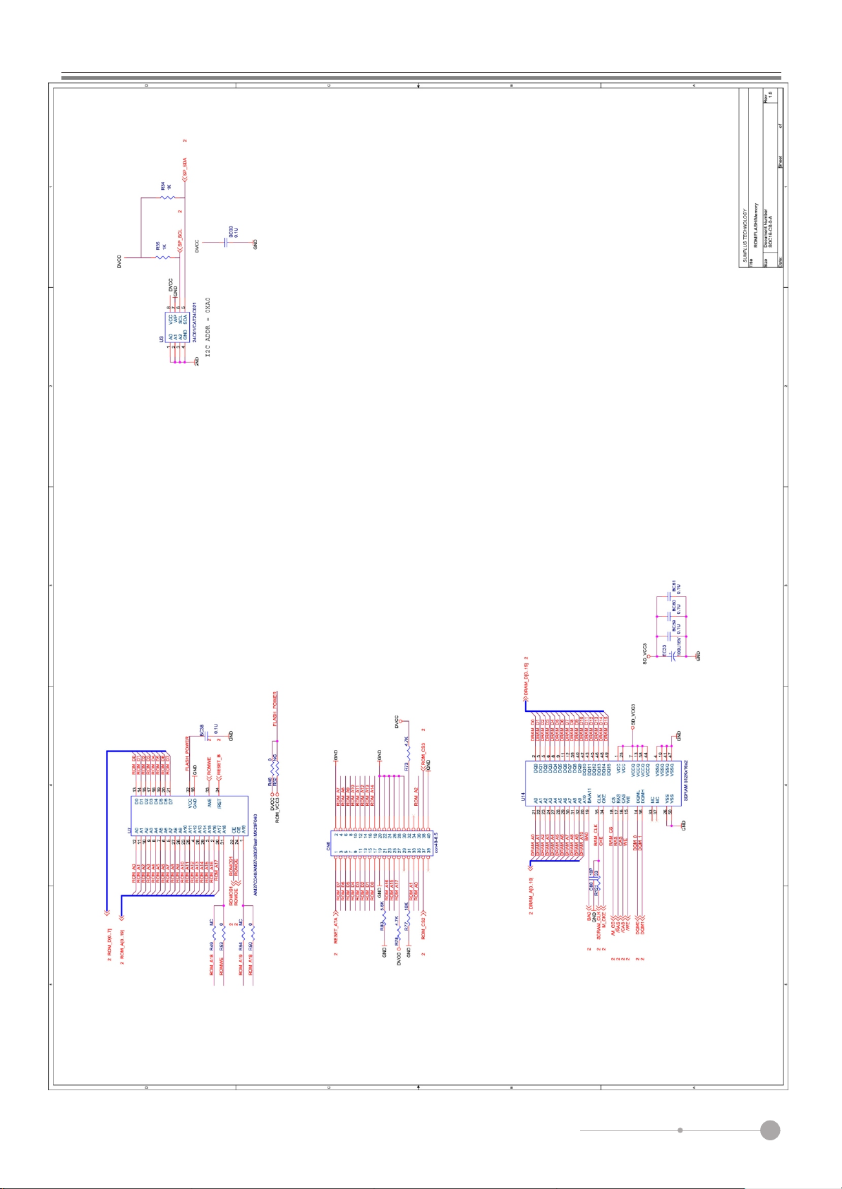
4. FUNCTIONAL DESCRIPTIONS
4.1 DVD MPEG board
DVD Service Manual
4M FLASH
SERIAL
EPROM
CVBS
R
G
B
16M
SDRAM
SPCA8200A
AUD2
AUD1
AUD0
2CHANNEL
AUDIO
Cntr/LFE
Rear L/R
Rear L/R
CODEC
DVD-DSP
I/F
CD-DSP
I/F
SPDIF
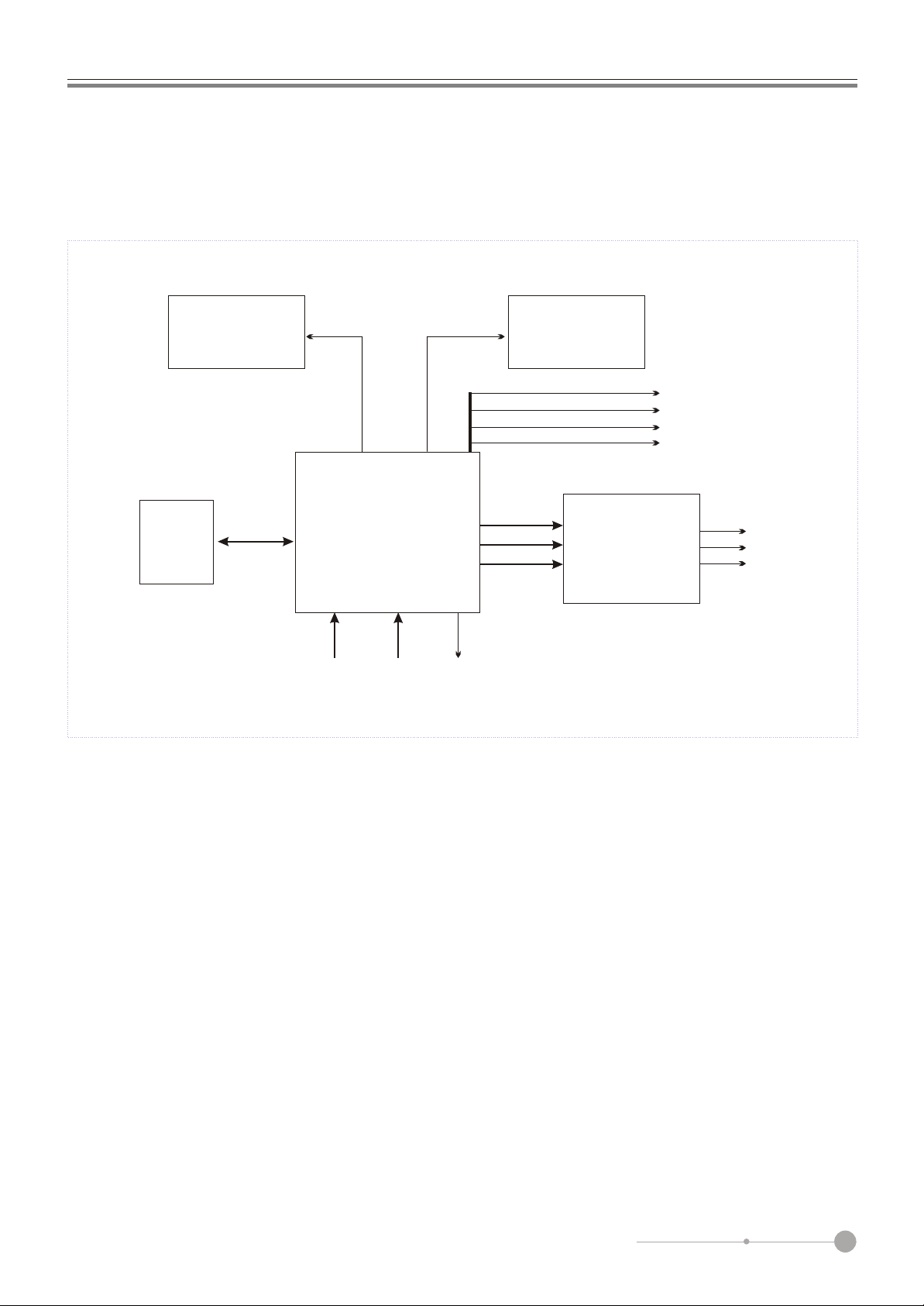
This board implements the back-end circuitry of a DVD player. It is composed of the following
subsystems:
* Microcontroller which does main control to all other sub-blocks of the system including user
interface, driver interface, audio/video output.
* Vaddis A/V Decoder IC decodes the bitstream coming from the DVD front-end drive, and
Optionally performs audio and video effects.
* Audio Codec
4
Page 6

DVD Service Manual
5
Page 7
DVD Service Manual
6
Page 8
DVD Service Manual
7
Page 9

DVD Service Manual
8
Page 10

DVD Service Manual
9
Page 11

DVD Service Manual
10
Page 12

DVD Service Manual
11
Page 13

DVD Service Manual
12
Page 14

DVD Service Manual
13
Page 15

4.2 Front Panel
The front panel I/O.
DVD Service Manual
A.
B
R3
STB
CLK
DATA
5V
GND
R
REM
10K
R2
10K
R1
10K
5V
E1
220U/10V
CLK
STB
DATA
1
C
S3
1 2S11 2S21 2
REMOTE
D
654321
5V
REM
65432
A
Number RevisionSize
B
Title
Date: 26-Jun-2004 Sheetof
File: DrawnBy:
1 2 3 4 5 6
D
C
B
A
14
Page 16

4.2.1 Front Panel Interface
6 Pin, Data Connector Pin Assignments
DVD Service Manual
PIN
1
2
3
4
5
6
NAME
DATA
STB
CLK
REM
GND
VCC
I/O
I
O
O
I
O
DESCRIPTION
Front Panel Data input
IR sensor interrupt
Front Panel chip select
Front Panel clock
Front Panel Data output
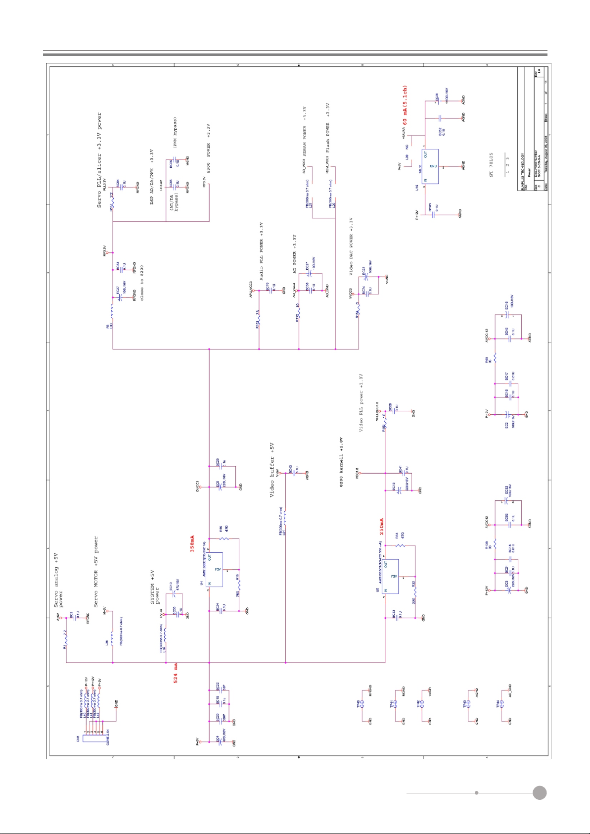
4.3 SMPS
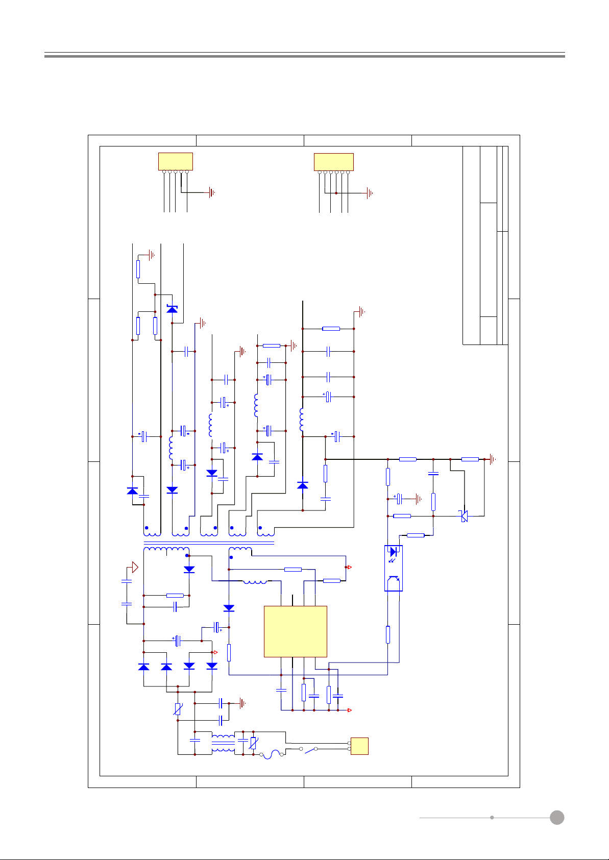
The mains power(220VAC) fed from N1 is filtered through C1, L1, C2 and L2 then rectified by D1, D2, D3 and D4
and generates an output at 300VDC. This 300VDC fed to T1 (pin2, pin4) which connects to TEA1523P(pin2), then
TEA1523P will automatically generate a 50KHz square waveform, this 50KHz square waveform controls the
ON/OFF between TEA1523P pin2 and the ground. In normal condition, T1 primary (between pin2 and pin4) will
create a 50KHz square waveform which is controlled by TEA1523P, this signal then fed to T1 and generates 2
different potential voltages of 12V and 5V between pin17, pin14 and pin16, pin14 respectively. The 12VDC and
5VDC then rectified by D7, D8, D9 and then filtered by L3, L4, L5, C9, C10 and C11. The feedback voltage is
controlled by Ic3 TL431 and IC2 PC817. When the output voltage is higher than 5V, the voltage at TL431(2.5V) is
compared with R10 and send out a signal to 5L0380R, the output square waveform then will change to adjust the
output voltage, this acts as a voltage stabilizer.
15
Page 17

DVD Service Manual
4.3.1 Adopt small lens: £ºcan adopt
4.4
4.4.1 Drive cell:adopt RF-300CA-11450 electricity machine
Electric specification
SONY310 .
act lens
4.2 Electricity machine work voltage is 3V-5.9V
4.3 General work voltage is 3.3V-5V
4.4 Unilateralism(com or go) move time:<1.5S(add 5V voltage)
4.5 In 5 C-10 C work current is <120mA
4.5 Testing condition
5.1 Position: level placed
5.2 environment: temperature 22+2 C
Humidity 50+5%
5.3 Turnover storehouse voltage:5V+0.5V
5.4 Standard DVD lens testing frock
5.5 Standard DVD testing dish
16
Page 18

DVD Service Manual
5. DESCRIPTION OF THE INTEGRATED CIRCUITS
5.1 SMPS TRANSFORMER
1. GENERAL INFORMATION
Main Voltage Operations:
Main Drop-out Voltage:
Mains STart-up Voltage:
Operating Frequency:
2. ELECTRICAL CHARACTERISTICS
2.1 STATIC CHARACTERISTICS
WINDING
Primary Inductance
1. Primary Leakage inductance (Pin 2-4) L1.5mH
2.2 WITHSTANDING VOLTAGE
The transformer shall sithstanding a voltage of 4 Kvms for 1 minute and 1 mA between
primary and seconday winding and also 2 Kvms for 1 minute and 1 mA between primary
winding with core and secondary winding with core.
PIN. NO
2-4
90Vac - 265 Vac
Max. 90 Vac
Max. 90 Vac
60 KHz
INDUCTANCE
1.5mH 10%
DESCRIPTION
<0.50W
2.3 INSULATION RESISTANCE
The insulation resistance shall be ore than 500M between primary and seconday
windings when the applied voltage 300 Vdc for 1 minute
2.4 ELECTRICAL CHARACTERISTICS
1. Before taking measurement Pp01 will be to give 5.0Vdc on 5.0Vdc line at Minimum
setting of controls and a mains voltage 220 Vac.
2. Before taking a measurement, DVD set should be working at least 5 minutes on
Normal condition
18
Page 19

5.3 SWPS CONTROLLER IC (TEP1523A)
DVD Service Manual
19
Page 20

5.3 SWPS CONTROLLER IC (TEP1523A)
DVD Service Manual
20
Page 21

DVD Service Manual
5.4 SMPS PROGRAMMABLE SHUNT REGULATOR
(FAIRCHILD TL 431)
Features
* Programmable output voltage to 36volts
* Low dynamic output impedance 0.20 typical
* Sink current capability of 1.0 to 100mA
* Equivalent full-range temperature
coefficient
of 50 ppm ℃ typical
* Temperature compensated for operation
over full rated operating temperature range
* Low output noise voltage
* Fast turn-on response
TO-92
1
1. Ref 2. Arode 3. Cathode
REFERENCE
Description
The TL 431/TL 431A are three-terminal
adjustable regulator series with a guaranteed
thermal stability over applicable temperature
ranges. The output voltage may be set to any
value between VREF (approximately 2.5
volts) and 36 volts with two external resistors.
These devices have a gypical dynamic
output impedanceof 2.0W Active oupput
circuity provides a very sharp turn-on
characteristic making these devices excel
lent replacement for zener diodes in many
applications
CATHODE
REFERENCE(R)
Absolute maximum ratings
Parameter
Cathode voltage
Cathode current Range (Continuous)
Reference Input Current Range
Power dissipation
D,Z Sffix Package
N Suffix Package
Operating Temperature Range
Storage Temperature Range
Recommended Operating conditions
Parameter
Cathode voltage
Cathode Current
2.5 Vref
Symbol
VKA
IKA
IREF
PD
TOPR
TSTG
Symbol
VKA
IKA
ANODE
CATHODE(K)
ANODE(A)
Value
37
-100 ~ +150
0.05 ~ +10
770
1000
-25 ~ +85
-65 ~ +150
Value ValueValue
- 36VREF
- 1001.0
Unit
V
MAI
MA
MW
MW
℃
℃
Unit
V
MA
21
Page 22

5.5 LINE FILTER (2 X 25mH)
ELECTRICAL DATA
Inductance: L1-2=L3-4-30mH - 15% - +20%
Resistance: R 1-2 = R 3-4 = 1.0 ohm (max)
Rated current: Irms = 0.50 A
(F= 1 Khz V= 1 Vms)
DVD Service Manual
CIRCUIT DIAGRAM
1 4
LEAKAGE INDUCTANCE
L 1-2 = L 3-4 100+/- 20%uH NOTES
2 3
22
Page 23

6. FAULT TRACING FLOW CHART
6.1 POWER SUPPLY
DVD Service Manual
NO PICTURE
CHECK
MPEG BOARD
Voltages Present?
YES
CHECK
MPEG BOARD
YES
REPLACE
CONNECT
CABLE
CHECK JP4
Connector
Voltages Present?
NO
NO
CHECK
FUSE
OK
Dp02
REPLACE Ip02,
OK
REPLACE
POWER PCB
NO
REPLACE
FUSE
23
Page 24

6.2 FRONT PANEL
NO PICTURE
NO FRONT
PANEL DISP
DVD Service Manual
CHECK
CN VOLTAGE
YES
MAINBOARD
Cn4 PIN2: RC
DATA
PRESS ANY KEY
ON RC AND
OBSERVE
SIGNAL
PRESS
"OPEN/CLOSE"
ON RC
(5V)
NO
NO SIGNAL
POWER
BOARD
CHECK
REPLACE
IR
RECEIVER
REPLACE
MPEG2
MAINBOARD
24
Page 25

6.3 MPEG BOARD
NO PICTURE NO AUDIO
DVD Service Manual
CHECK
JP4
VOLTAGE(5V,12V)?
YES
LOADER
RUNING?
YES
J3(RGB&CVBS
RUNING?)
NO
NO
NO
POWER
BOARD
CHECK
REPLACE
MPEG
BOARD
NO
INSERT A CD FOR
AUDIO TEST AND
PRESS PLAY
CHECK CN6
AUDIO OUTPUT
25
Page 26

7. COMPONENT LIST
CABLE
POS NO TELRA CODE DESCRIPTION
SWPS
POS NO TELRA CODE DESCRIPTION
C1 104K M 275V~X2 335 5 MKP
C2 104K M 275V~X2 335 5 MKP
C3
C4
C5
C6
C7 Cap.,50V 473,10%
C8
C9 Ceramic Cap.,63v 104,10%
CA1
CE4 Elec. Cap.,400V-47UF,M,18X27mm
CE2 Elec. Cap.,50V-22UF,M,5X11.5mm
CE6 Elec. Cap.,35V-220UF,M,8X11.5mm
CE11 Elec. Cap.,35V-220UF,M,8X11.5mm
CE10
CE13 Elec. Cap.,10V-2200UF,M,10X20mm
CE14 Elec. Cap.,16V-220UF,M,6.3X11mm
CE15 Elec. Cap.,10V-100UF,M,5X11mm
BR1 Rectifier Diode,1N4007,DO-41
BR2 Rectifier Diode,1N4007,DO-41
BR3 Rectifier Diode,1N4007,DO-41
BR4 Rectifier Diode,1N4007,DO-41
D1 Rectifier Diode,HER105,DO-41
D2 Switch Fr102
D3 Rectifier Diode,FR102,DO-27
D4 Rectifier Diode,FR104,DO-27
D5 Rectifier Diode,FR104,DO-27
D6 Rectifier Diode,FR157,DO-41
D7 Rectifier Diode,SR360,DO-41
D8 Zener Diode,9.1V
FHB FB, 3.5mm*4.7mm*0.8mm
FUSE Fuse,T1AL250V,5*20mm,Glass
IC-1 IC,TEA1523P DIP8
IC-2 IC,PC817B
IC-3 IC,TL431C,TO-92
J-1 Jumper,Diameter=0.6mm,L=10mm
J-2 Jumper,Diameter=0.6mm,L=5mm
J-3 Jumper,Diameter=0.6mm,L=7.5mm
DVD Service Manual
6Pin,2.0mmPitch to 6Pin,2.0mmPitch VH,180mm,UL2468
26AWG
5Pin,2.0mmPitch to 5Pin,2.0mmPitch PH,150mm,UL2468
26AWG
6Pin,2.54mmPitch to 6Pin,2.54mmPitch VH,250mm,UL2468
26AWG
5Pin,2.54mmPitch,VH to MPEG Power Socket,280mm,UL1007
20AWG
Power Cable,180m,VDE
AV Cable,1.5m
Ceramic Cap.,
Ceramic Cap.,
Ceramic Cap.,1KV 103M 10%
Ceramic Cap.,1KV-101,K
Ceramic
Ceramic Cap.,63V 104,10%
Ceramic Cap.,
Elec. Cap.,25V-1000UF,M,10X20mm
471K M 275V~X1,Y1 335
471K M 275V~X1,Y1 335
222 M 400V~X1,Y1 335
,DO-41
26
Page 27

POS NO TELRA CODE DESCRIPTION
L-1 Filter,ET20
L-2 Filter,SG01183
L-3
L-4
L-5
Cn1 Conn.,2Pin,VH,3.96mm,S
Cn2 Conn.,2Pin,VH,3.96mm,S
C0N1 Conn.,5Pin,2.54mm,S
CON2 Conn.,6Pin,2.54mm,S
N4 Conn.,4Pin,2.54mm,S
PCB PCB,POW389L
R1 Carbon Film Res.,2W-56K,J
R2 Carbon Film Res.,1/4W-22E,J
R3 Carbon Film Res.,1/4W-330E,J
R4 Carbon Film Res.,1/4W-1K,J
R5 Carbon Film Res.,1/4W-1M,J
R6 Carbon Film Res.,1/4W-10K,J
R7 Carbon Film Res.,1/4W-10K,J
R8 Carbon Film Res.,1/4W-10K,J
R9 Carbon Film Res.,1/4W-1E,J
R10
TR-1 NTC 10D-11
T1 Transformer,KB-464-3089
Radial Choke Inductor,15uH 10%
Radial Choke Inductor,15uH 10%
Radial Choke Inductor,15uH 10%
Carbon Film Res.,1/4W-680E,J
DVD Service Manual
FRONTPANEL
POS NO TELRA CODE DESCRIPTION
CD1
RD1
RD2
RD3
REM01 Remote Receiver,GPIUM271RK
SW1
SW2
SW3
Elec. Cap.,220uF-10V,5*7mm,CD11,M
Carbon Film Res.,1/8W,10K,J
Carbon Film Res.,1/8W,10K,J
Carbon Film Res.,1/8W,10K,J
Tact Switch,6*6*5mm
Tact Switch,6*6*5mm
Tact Switch,6*6*5mm
27
 Loading...