

Page 1
CRT COLOR TV SET
21CTU93BC
Page 2
SERVICE MANUAL
AKAI 21CTU93BC
This manual is the latest at the time of printing, and does not
include the modification which may be made after the printing, by
the constant improvement of product
Page 3

- Content ......................................................................................................................... 2
- Bill of Materials ............................................................................................................. 3
- Safety Precautions ....................................................................................................... 7
- TV Block Diagram ......................................................................................................... 8
- Replacement Of Memory IC ......................................................................................... 10
- Service Adjustment ...................................................................................................... 10
- ICs Functional Description .......................................................................................... 18
- Test point Waveforms .................................................................................................. 22
- Purity / Convergence Adjustment ............................................................................... 23
- Explore View Diagram .................................................................................................. 25
Page 4
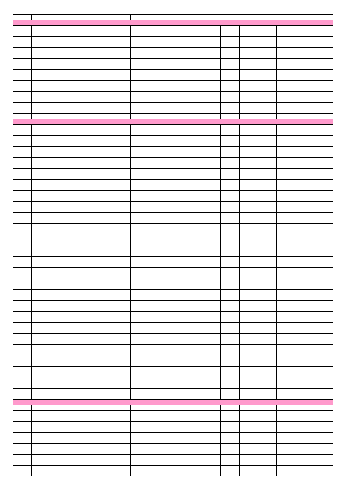
SER DESCRIPTION QTY
PCB NO.
CABLE & SOCKET
1 AV6-14 1 XS801
2 CH5B-2.5-2DY 3 XS601 XS602 XS702
3 CH5B-2.5-4DY 4 XS403 XS703 XS704 XS804
4 CH5B-2.5-5DY 1 XS201
5 CH7-10-1DY 1 K9N
6 CH7-10-2DY 2 XS501 XS502
7 CH7-8-10-4DY 1 XS402
8
CH9-2.5-2DY-400-CH5B-W (卧式)
9
CH9-2.5-4DY-400-CH5B-4W(卧式)(带屏蔽)
1 XS701
1 XS702
10 CH9-2.5-4DY-450-CH5B 1 XP902
11 CH9-2.5-4DY-550-CH5B 1 PA102
12 CH9-2.5-5DY-500-CH5B 1 XP901
13 H03VVH2-F0.75mmX2C (250MM) short power cord 1
14 Power cord (2200mm ) 1
15 RCA-106A (red) 1 AV3
16 RCA-106A (white) 1 AV2
17 RCA-106A (yellow) 1 AV1
CARBON RESISTOR
18
RT-1/2W-1KΩ-J
19
RT-1/2W-220KΩ-J
20
RT-1/2W-220Ω-J
21
RT-1/2W-22KΩ-J
22
RT-1/4W-1.8KΩ-J
23
RT-1/4W-150Ω-J
24
RT-1/4W-1KΩ-J
25
RT-1/4W-1Ω-J
26
RT-1/4W-2.2Ω-J
27
RT-1/4W-2.7KΩ-J
28
RT-1/4W-220KΩ-J
29
RT-1/4W-27Ω-J
30
RT-1/4W-33Ω-J
31
RT-1/4W-8.2Ω-J
32
RT-1/4W-82Ω-J
33
RT-1/6W-1.2K
34
RT-1/6W-1.5KΩ-J
35
RT-1/6W-1.8KΩ-J
36
RT-1/6W-100KΩ-J
RT-1/6W-100Ω-J
38
RT-1/6W-10KΩ-J
39
RT-1/6W-12KΩ-J
40
RT-1/6W-150KΩ-J
41
RT-1/6W-15KΩ-J
42
RT-1/6W-1KΩ-J
43
RT-1/6W-2.7KΩ-J
44
RT-1/6W-220KΩ-J
45
RT-1/6W-220Ω-J
46
RT-1/6W-22KΩ-J
47
RT-1/6W-27KΩ-J
48
RT-1/6W-3.3KΩ-J
49
RT-1/6W-3.9KΩ-J
50
RT-1/6W-330Ω-J
51
RT-1/6W-33KΩ-J
52
RT-1/6W-390Ω-J
53
RT-1/6W-39KΩ-J
54
RT-1/6W-39Ω-J
55
RT-1/6W-3KΩ-J
56
RT-1/6W-4.7KΩ-J
57
RT-1/6W-4.7Ω-J
58
RT-1/6W-470Ω-J
59
RT-1/6W-47KΩ-J
60
RT-1/6W-47Ω-J
61
RT-1/6W-5.1KΩ-J
62
RT-1/6W-680Ω-J
63
RT-1/6W-8.2KΩ-J
Ω-J
1 R403
1 R501
1 R564
1 R487
1 R507
1 R575
2 R406 R457
1 R302
1 R304A
1 R508
1 R401
1 R720
2 L201 R940
1 R511
1 R562
1 R105
1 R706
2 R301 R303
5 R313 R554 R716 R802 R837
R110 R111 R208 R209 R210 R212 R306 R307 R710 R711
1837
R712 R714 R715 R823 R824 R825 R826 R838
R109 R211 R576 R602 R611 R612 R614 R702 R723 R811
18
R812 R815 R817 R821 R836 R912 R922 R932A
1 R207
2 R605 R700
3 R725 R609 R610
R553 R558 R565 R566 R573 R713 R730 R803 R805 R816
13
R818 R820 R822
1 R705
2 R407 R226
6 R101 R309 R806 R913 R923 R933
2 R706 R221
2 R402 R701
3 R613 R703 R704
1 R704
3 R916A R926 R936
2 R205 R705
1 R201
4 R204 R222 R604 R603
1 R103
1 R559
R104 R108 R213 R311 R707 R709 R718 R719 R721 R727
13
R728 R703 R719A
1 R217
6 R102 R218 R219 R220 R312 R807
3 R106 R726 R606
6 R911 R914 R916 R924 R932 R934
1 R414
3 R202 R707 R719B
1 R702
CERAMIC CAPACITOR
64
CT-1KV-1000pF-K(湿封装)
2 C504 C505
65 CT-2KV-1000pF-K 1 C943
66 CT-2KV-471pF-K 1 C553
67 CT-2KV-680pF-K 2 C513 C511
68 CT-500V-1000pF-K 1 C452
69 CT-500V-3900pF-K 2 C451 C510
70 CT-63V-0.01uF-Z 9 C104 C105 C106 C216 C569 C612 C613 C701 C711
71 CT-63V-0.1uF-K 5 C220 C222 C223 C707 C713
72 CT-63V-1000pF-J 6 C202 C203 C205 C206 C213 C214
73 CT-63V-220pF-J 3 C313 C702 C703
74 CT-63V-390pF-J 3 C921 C931 C911
75 CT-63V-560pF-J 1 C225
76 CT7-2E4-400VAC-3300pF-M 1 C517
Page 5

SER DESCRIPTION QTY
PCB NO.
COIL, IN,LF,TFM
77 130-208-0011 1 L405
78 3.0mH 1 L404
79 BCK-42-09936 1 T501
80 JBC-184-EI19/YDD-EI19 1 T451
81 JLC/YDD-600µH 1 L311
82 JLC-128-23µH 1 L441
83 LG0307-1.2UH-K 1 L101
84 LG0307-10UH-K 6 L202 L203 L701 L702 L703 L704
85 YDD-UF16/JLF-98-UF16 1 L501
DIODE
86 BAV21 3 D912 D922 D932
87 FR107 3 D301 D302 D401
88 FR154 2 D510 D513
89 FR157 1 D462
90 FR305/RU4C 2 D452 D559
91 FR309/RU4DS 1 D451
92 HER154/HER204 1 D553
93 HER204 3 D552 D554 D555
94 IN4148 8 D404 D461 D516 D558 D565 D566 D601 D701
95 IN5399/RL207 4 D501 D502 D503 D504
96 RU4A /RU4AM 1 D551
ELECTROLYTE CAPACITOR
97 CD110-160V-100UF-M 2 C403 C551
98 CD110-16V-100UF-M 5 C208 C219 C221 C224 C568
C101 C108 C102 C103 C204 C217 C708 C603 C710 C801
2199 CD110-16V-10UF-M
C802 C804 C805 C806 C807 C808 C809 C813 C814 C815
C816
100 CD110-16V-220UF-M 1 C211
101 CD110-16V-470UF-M 4 C566 C567 C609 C803
102 CD110-16V-47UF-M 6 C563 C564 C565 C709 C712 C701
103 CD110-250V-10UF-M 1 C459
104 CD110-25V-470UF-M 5 C314 C315 C555 C556 C601
105 CD110-35V-100UF-M 1 C304
106 CD110-35V-470UF-M 1 C305
107 CD110-35V-47UF-M 2 C401 C508
108 CD110-50V-0.22UF-M 2 C607 C608
109 CD110-50V-1UF-M 5 C218 C611 C605 C810 C811
110 CD110-50V-4.7UF-M 1 C561
111 CD288H-250V-10UF-M 1 C402
112 CD293-400V-150UF-M 1 C507
113 CD71-50V-10µF-M 1 C312
FBT
114 BSC25-0226Q 1 T401
GLASS ENAMEL RESISTOR
115
RI-1/2W-12MΩ-K
1 R514
HEATSINK
116 HS-EW04-60 1 V303
117 HS-PH01-50 1 V451
118 HS-PW01-50 1 N502
119 HS-VS02-70 1 N301
120 HS-WS03-40 1 N601
INTEGRATE CIRCUIT
121 5Q0765RF 1 N502
122 AT24C08/ATMEL24C08 1 N701
123 PC817B/LTV-817/817B 1 N501
124 STV9325/STV8172A 1 N301
125 TC4052/HEF4052BP 1 N801
126 TDA11136 1 N201
127 TDA7266SA 1 N601
128 TL431 1 V551
129 UPC574/KA33V 1 N561
JUMPERS
W214 W216 W402 W504 W505 W509 W510 W563 W591 W602
21130 10MM
W701 W702 W704 W712 W801 W802 W803 W804 W805 W806
L901
131 12.5MM 10 W502 W205 W204 W561 W593 W606 W709 W714 L301 L403
132 15MM 3 W551 R513 R568
133 17.5MM 2 W406 W405
134 5MM 4 W104 W215 C453 W807
W101 W102 W103 W201 W202 W203 W206 W207 W208 W209
W210 W211 W212 W403 W503 W506 W512 W513 W552 W601
31135 7.5MM
W603 W604 W605 W708 W710 W713 D557 R319 D911 D921
D931
LED
136
LED(red)
1 LED4
OTHER
137 BXGJ-1 2 F501
138 GZS10-108C 1 XS902
139 KDVF38.9H/F38.9H/LBN38.9H 1 Z101
140 PG-238 (INFRARED RECEIVER) 1 RE
141 T3.15A250V-AC 1 F501
142 X24.576M/T24.576M 1 G701
Page 6
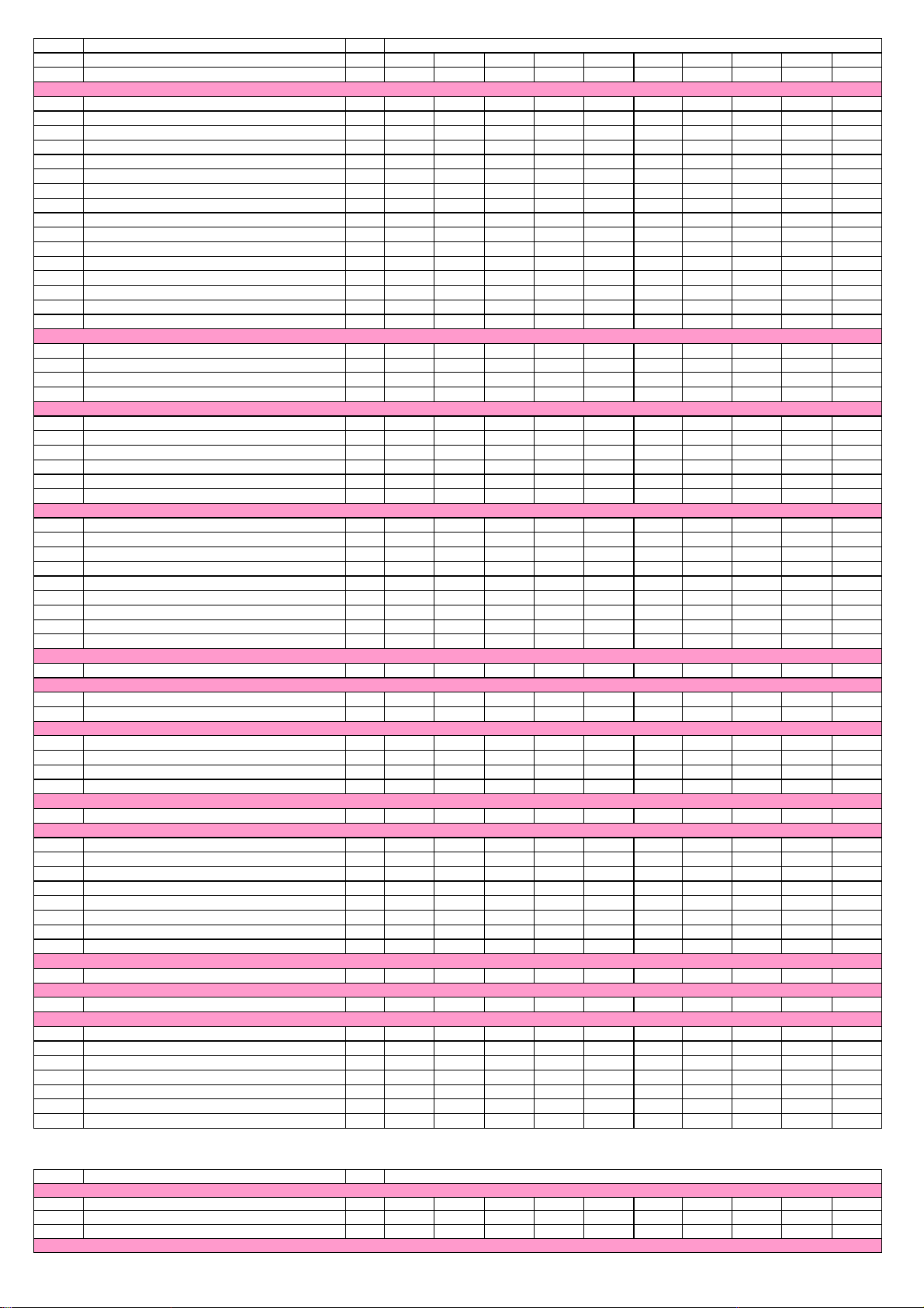
SER DESCRIPTION QTY
孔
143
贴于场IC
144
贴于电源管
PCB NO.
1
1
OXIDE FILM RESISTOR
145
RF-2W-1.5Ω-J
146
RY-1/2W-120KΩ-J
147
RY-1/2W-2.7KΩ-J
1 R451
3 R503 R504 R555
3 R918 R928 R938
148 RY-1/6W-39K-G 1 R206
149
150
151
152
153
154
155
156
157
158
159
160
RY-1W-180Ω-J
RY-1W-1KΩ-J
RY-1W-1Ω-J
RY-2W-0.47Ω-J
RY-2W-12KΩ-J
RY-2W-15KΩ-J
RY-2W-2.2Ω-J
RY-2W-270Ω-J
RY-2W-4.7Ω-J
RY-2W-47KΩ-J
RY-2W-5.6Ω-J
RY-2W-8.2Ω-J
1 R305
1 R404
1 R304
1 R601
3 R915 R925 R935
1 R569
1 R561
1 R454
1 R567
1 R512
1 R317
1 R571
PCB
161 IU-2103KY-001 1
162 IU-2103RE-001 1
163 IVPH-002/21 ver1.1 1
164 JS02-3AV-14 VER1.2 1
POLYESTER CAPACITOR
165 CL11-100V-0.0047uF-K 1 C522
166 CL11-100V-0.0068uF-K 1 C215
167 CL11-100V-0.015uF-K 1 C301
168 CL11-100V-0.033uF-K 3 C404 C519 C559
169 CL11-100V-0.047uF-K 2 C302 C310
170 CL11-100V-0.1uF-K 8 C201 C209 C303 C458 C704 C705 C706 C520
POLYPROPYLENE CAPACITOR
171 CBB21-250V-0.22uF-J 1 C461
172 CBB21-400V-0.3uF-K 1 C460
173 CBB21-630V-0.027uF-K 1 C457
174 CBB21-630V-0.068uF-J 1 C462
175 CBB23A-250VAC-0.1µF-M 1 C501
176 CBB81-1.6KV-2200PF-K 1 C454
177 CBB81-1.6KV-8200pF-K 1 C456
178 CBB81-1.6KV-9100PF-K 1 C455
179 CL21X-63V-0.15uF-K 1 C207
POWER SWITCH
180 KDC-A04-001S 1
PTC & NTC THERMISTOR
181 8D-11 1 R502
182
MZ73-9Ω(3脚)
1 RT501
SCREWS
183 2.0 X 3.5MM 9
L441(短
T501(4) T401(3)
184 2.3 X 3.5MM 2 C507(2)
185 TR 3×10 (with pad) 3 V303 N601(2)
186 TR 3×10 (without pad) 3 N301 N502 V451
TACT SWITCH
187 KFC-A06-P5 6 SW1 SW2 SW3 SW4 SW5 SW6
TRIODE
188 2SA1015-Y 3 V563 V601 V803
189 2SC1674 1 V101
190 2SC1815-Y 9 V201 V202 V203 V311 V562 V602 V702 V801 V802
191 2SC2383 4 V401 V561 V564 V565
192 2SC2482 3 V911 V921 V931
193 2SC5296 1 V451
194 A940 1 V303
195 BF421/BF423 3 V913 V923 V933
TUNER
196 EWE-5053-V8/ET-5K1E-EV100K 1 A101
VARIABLE RESISTOR
197
W206-2AL20KΩ-K
1 RP551
ZENER DIODE
198 MTZJ3V3/3C2 1 D703
199 MTZJ3V6/4A2 1 D509
200 MTZJ5V1/5C2 2 D801 D802
201 MTZJ5V6/6B1 2 D567 D564
202 MTZJ8V2 1 D941
203 MTZJ8V2/9A2 1 D402
204 MTZJ8V7/9B2 1 D561
CE STANDARD COMPONENT
SER DESCRIPTION QTY
CERAMIC CAPACITOR
1
CT-1KV-1000pF-K(湿封装)
2 CT7-2E4-400VAC-2200pF-M +2 C515 C516
3 CT7-2E4-400VAC-3300pF-M -1 C517
COIL, IN,LF,TFM
PCB NO.
+2 C503 C506
Page 7

SER DESCRIPTION QTY
4 F22-22R0-031000/JLF-148-ET24 +2 L501 L502
5 YDD-UF16/JLF-98-UF16 -1 L501
JUMPERS
6 10MM -2 W509 W510
POLYPROPYLENE CAPACITOR
7 CBB23A-250VAC-0.1µF-M -1 C501
8 CBB23A-250VAC-0.1µF-M +1 C512
9 CBB23A-250VAC-0.22µF-M +2 C501 C502
PCB NO.
Page 8
SAFETY PRECAUTIONS
1. The design of this product contains special hardware, many
circuits and components specially for safety purposes. For
continued protection, no changes should be made to the
original design unless authorized in writing by the
manufacturer. Replacement parts must be identical to those
used in the original circuits. Service should be performed by
qualified personnel only.
2. Alterations of the design or circuitry of the products should
not be made. Any design alterations or additions will void
the manufacturer’s warranty and will further relieve the
manufacturer of responsibility for personal injury or property
damage resulting therefrom.
3. Many electrical and mechanical parts in the products have
special safety-related characteristics. These characteristics
are often not evident from visual inspection nor can the
protection afforded by them necessarily be obtained by
using replacement components rated for higher voltage,
wattage, etc. Replacement parts which have these special
safety characteristics are identified in the parts list of
Service manual. Electrical components having such
features are identified by shading on the schematics
and by ( ! ) on the parts list in Service manual. The use
of a substitute replacement which does not have the same
safety characteristics as the recommended replacement
part shown in the parts list of Service manual may cause
shock, fire, or other hazards
4. Don’t short between the LIVE side ground and
ISOLATED (NEUTRAL) side ground or EARTH side
ground when repairing. Some model’s power circuit is
partly different in the GND. The difference of the GND is
shown by the LIVE: ( ) side GND, ISOLATED (NEUTRAL) :
( ) side GND and EARTH : ( ) side GND. Don’t short
between the LIVE side GND and ISOLATED (NEUTRAL)
side GND or EARTH side GND and never measure with a
measuring apparatus (oscilloscope etc.) the LIVE side GND
and ISOLATED (NEUTRAL) side GND or EARTH side GND
at the same time. If above note will not be kept, a fuse or
any parts will be broken.
5. If any repair has been made to the chassis, it is
recommended that the B1 setting should be checked or
adjusted (See ADJUSTMENT OF B1 POWER SUPPLY).
6. The high voltage applied to the picture tube must conform
with that specified in Service manual. Excessive high
voltage can cause an increase in X-Ray emission, arcing
and possible component damage, therefore operation under
excessive high voltage conditions should be kept to a
minimum, or should be prevented. If severe arcing occurs,
remove the AC power immediately and determine the cause
by visual inspection (incorrect installation, cracked or melted
high voltage harness, poor soldering, etc.). To maintain the
proper minimum level of soft X-Ray emission, components
in the high voltage circuitry including the picture tube must
be the exact replacements or alternatives approved by the
manufacturer of the complete product.
7. Do not check high voltage by drawing an arc. Use a high
voltage meter or a high voltage probe with a VTVM.
Discharge the picture tube before attempting meter
connection, by connecting a clip lead to the ground frame
and connecting the other end of the lead through a 10kΩ
2W resitor to the anode button.
8. When service is required, observe the original lead dress.
Extra precaution should be given to assure correct lead
dress in the high voltage circuit area. Where a short circuit
has occurred, those components that indicate evidence of
overheating should be replaced. Always use the
9. manufacturer’s replacement components.
.
10. Isolation Check
(Safety for Electrical Shock Hazard)
After re-assembling the product, always perform an isolation
check on the exposed metal parts of the cabinet (antenna
terminals, video/audio input and output terminals, Control
knobs, metal cabinet, screwheads, earphone jack, control
shafts, etc.) to be sure the product is safe to operate without
danger of electrical shock.
11. The surface of the TV screen is coated with a thin film which
can easily be damaged. Be very careful with it when handle
the TV. Should the TV screen become soiled, wipe it with a
soft dry cloth. Never rub it forcefully. Never use any cleaner
or detergent on it.
(1) Dielectric Strength Test
The isolation between the AC primary circuit and all metal
parts exposed to the user, particularly any exposed metal
part having a return path to the chassis should withstand a
voltage of 3000V AC (r.m.s.) for a period of one second.
(…Withstand a voltage of 1100V AC (r.m.s.) to an appliance
rated up to 120V, and 3000V AC (r.m.s.) to an appliance
rated 200V or more, for a periode of one second.)
This method of test requires a test equipment not generally
found in the service trade.
(2) Leakage Current Check
Plug the AC line cord directly into the AC outlet (do not use
a line isolation transformer during this check.). Using a
“Leakage Current Tester”, measure the leakage current
from each exposed metal part of the cabinet, particularly
any exposed metal part having a return path to the chassis,
to a known good earth ground (water pipe, etc.). Any
leakage current must not exceed 0.5mA AC (r.m.s.).
However, in tropical area, this must not exceed 0.2mA AC
(r.m.s.).
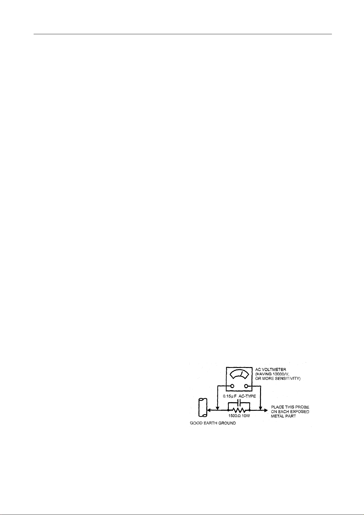
●Alternate Check Method
Plug the AC line cord directly into the AC outlet ( do not use
a line isolation transformer during this check.). Use an AC
voltmeter having 1000 ohms per volt or more sensitivity in
the following manner. Connect a 1500Ω 10W resistor
paralleled by a 0.15μ F AC-type capacitor between an
exposed metal part and a known good earth ground (water
pipe, etc.). Measure the AC voltage across the resistor with
the AC voltmeter. Move the resistor connection to each
exposed metal part, particularly any exposed metal part
having a return path to the chassis, and measure the AC
voltage across the resistor. Now, reverse the plug in the AC
outlet and repeat each measurement. Any voltage
measured must not exceed 0.75V AC (r.m.s.). This
corresponds to 0.5mA AC (r.m.s.).
However, in tropical area, this must not exceed 0.3V AC
(r.m.s.).
This corresponds to 0.2mA AC (r.m.s.)
7
Page 9
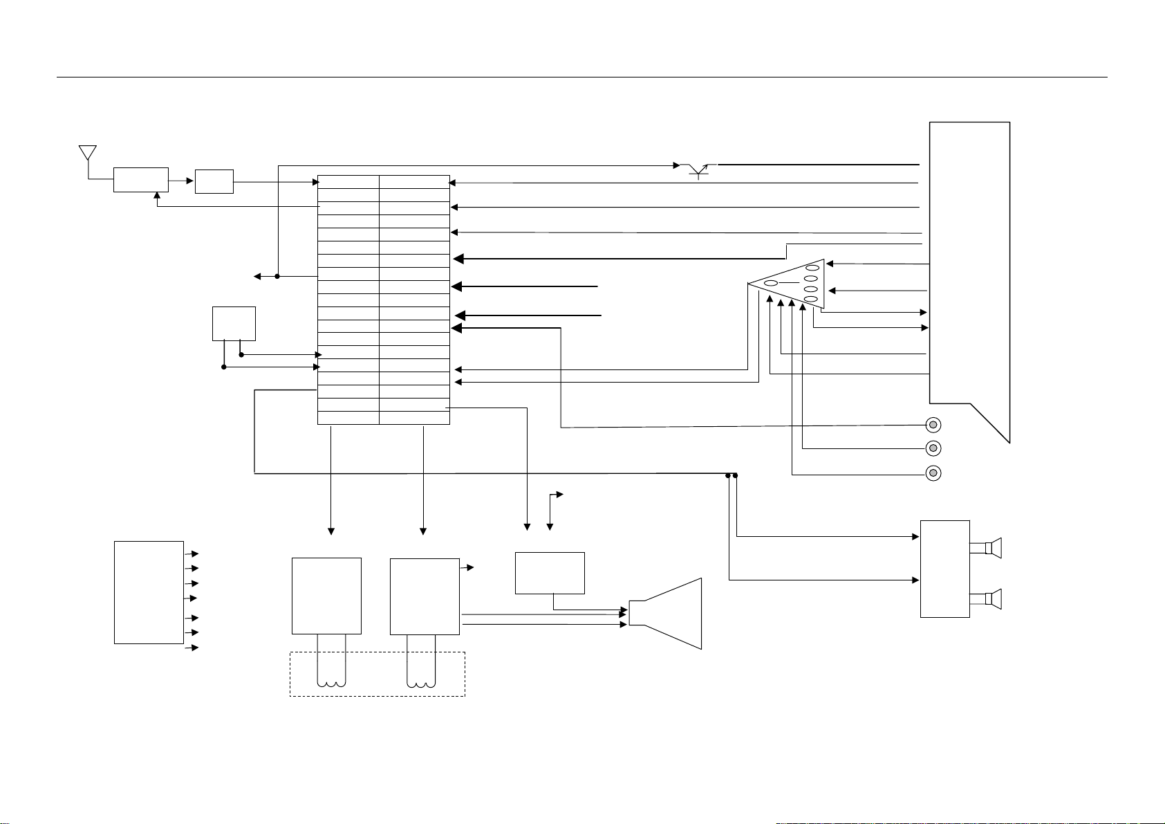
TV Block diagram
VoV
A
A
A
A
A
V24V
V8V5V
V
Y
V
N
S
A
ALoA
A
2
V
V
TUNER
POWER
UNIT
SAW
video
24C08
bus
130
+13
-13
3.3
TDA11105-XXXX
IF IN R IN
RF AGC GIN
B IN
CHROMA
VIDEO
CVBS/Y IN
CVBS1 IN
CVBS2 IN
SDA
SCL MA IN L
MAOUTR MA IN R
MAOUTL
RGB OUT
V OUT H OUT
V IN
TDA8177
V OUT
D
H IN
H OUT
H OUT
200
CRT PCB
SCREE
FOCU
audio
8
.
video
R
G
B
405
video
Video IN
audio
audio
CRT
C
R i1
Li 1
Ro
Ri 2
Li 2
video
2i
Li2
Li1
N17821
Vi1
OUT1-
OUT1+
Vi2
OUT2-
OUT2+
8
Page 10

.
9
Page 11

REPLACEMENT OF MEMORY IC
1. MEMORY IC.
This TV uses memory IC. In the memory IC are memorized data for correctly operating the video and
deflection circuits.
When replacing memory IC, be sure to use IC written with the initial value of data.
2. PROCEDURE FOR REPLACING MEMORY IC
(1) Power off
Switch the power off and unplug the power cord from AC outlet.
(2) Replace IC
Be sure to use memory IC written with the initial data values.
(3) Power On
Plug the power cord into the AC outlet and switch the power On.
(4) Check and set SYSTEM default value:
3. Note: enter a factory mode method
1) Factory remote control: Press the factory remote control up [PRESET], press again[TEST]key,
appear on the television screen 'M'.
2) Customer remote control
3) Press [menu] key, appear the picture menu, press few character keys 6483, the screen
appears M.
4) Press [standby] key, withdraw factory mode.
5) The “TEST” will be displayed on the screen.
6) Check the setting value of the SYSTEM default value of Table below. If the value is different,
select items by [CH+]/[CH-] keys and set value by [VOL+]/[VOL-] keys.
7) Press “STANDBY” key again and return to the normal screen.
SERVICE ADJUSTMENT
B1 POWER SUPPLY
1. Receive normal colour bar signal.
2. Connect DC voltmeter to VD541- and isolated ground.
3. Adjust potentiometer in power unit to get the voltage as 110V ±1.0V for 21 inch hereinafter,
130 ±1.0V for 25 inch upwards.
FOCUS ADJUSTMENT
1. Receive a crosshatch signal.
2. While watching the screen, adjust the FOCUS VR to make the vertical and horizontal lines as fine and
sharp as possible.
BUS CONTROL ADJUSTMENT
To enter BUS control mode, Press “TEST” key on the Remote control unit of factory. (Customer remote
control press "MENU" key behind in a row press"6""4""8""3")
Choose a "SETUP SELECT" options in"M2" menu, one by one in order press the numerical key"6, 4, 8 and 3",
press "MUTE" key again can depend on this get into "M3"~"M9" of design menu, general factory the
10
Page 12

production doesn't need to carry on M 3~ adjustments of M9.
In "M0"~under"M9" appearance press” CALL” the key can get into "M" appearance.
At “M”under the appearance press “-/-“ the key can get into “BUS OPEN” appearance, at “BUS OPEN under,
press “-/-“ the key recover factory appearance.
Remote Hand Unit keys
[M1] [M2] [M3]
[M1] menu
MENU0 Geometrical adjustment
Receive PAL standard Complete pattern signal.
Receive NTSC signal and repeat above [M0] and [M1] adjustment.
[M2] Menu
AGC Adjustment.
[M3] Menu
CRTcut off and white balance adjustment.
Receive white signal.
c d e
f g h
Horizontal line
i
j k
[M0]
b
Adjustment steps:
a) Adjust V. SLOPE, to the center horizontal line just appeare from half bottom shadow.
b) Adjust V. SIZE, to get 90% of vertical picture contents would be displayed on CRT.
c) Adjust V. SHIFT, the center horizontal line correspond to CRT vertical center.
d) Adjust H.SHIFT, to get the picture horizontal center correspond to CRT horizontal center.
Receive 60dBμ(1mV)V
reduce gradually and just disappeared point.
Select “shipping”, push [V+] [V-]key to be shipped.
a) CRT cut off adjustment.
1. Select “SC”, then automatically vertical scan will be stopped.
2. Adjust SCREEN control on Flyback transformer to get the darkest single horizontal line (red,
green, or blue, sometimes shows more yellow, more purple or more white).
b) White balance adjustment.
1. Select RD/BD menu.
2. Adjust RD/BD to get colour temperature as x=281, y=311
c) Sub-Brightness adjustment. (Use stair case signal)
1. Select SB menu.
2. Adjust SB to get the darkest step being cutoff.
colour bar pattern signal,adjust AGC value(voltage from high to low),to noise
H
11
Shado
a
Page 13

I2C standard UOC for export bus control adjustment item default setting 2007-12-05
MI Items Variable Preset recommendation
M0 50HZ 60HZ 50HZ 60HZ
V. LOPE 63 + / -32 Picture vertical center adjustment 35 -01
V. SIZE 63 + / -32 Vertical amplitude adjustment 20 +02
V. SC 63 + / -32 Vertical S Correction Adjustment 25 -01
V.LINE 63 + / -32 Vertical positions adjustment 18 +02
V.SCR 63 +/-32 Vertical S Correction R 32 -01
H.PSASE 15 +/-32 Horizontal position adjustment 40 0
EW.W 63 + / -32 Horizontal amplitude adjustment 55 0
EW.PW 63 +/-32 E/W amplitude adjustment 29 0
EW.TC 63 +/-32 Picture trapezoid adjustment 31 0
EW.UCP 63 +/-32 Picture top Cape adjustment 48 0
EW.LCP 63 +/-32 Picture bottom Cape adjustment 45 0
H.BOW 63 +/-32 Picture bow form adjustment 30 0
H.PAR 63 +/-32 Picture parallelogram adjustment 31 0
H.BLK.SW ON/OFF Horizontal blank switch ON
M1 TV /DVD
CL 0~15 Contrast level offset 13
BLOC 0~15 Black level offset course 6
R.BIA 0~63 R OUT Amplitude Adjustment 32
G.BIA 0~63 32 G OUT Amplitude Adjustment 32 -6
B.BIA 0~63 B OUT Amplitude Adjustment 32
R.DRV 0~63 R OUT Amplitude Adjustment 32
G.DRV 0~63 G OUT Amplitude Adjustment 32
B.DRV 0~63 B OUT Amplitude Adjustment 32
SUB BRT 0~63 Brightness of screen line 32
VSD 0~1 Vertical Ramp Out Stop Selection
TEST.S 0~5
M2 50HZ 60HZ
RF AGC 0~63 32 Tuner AGC Takeover Point Adjustment
OSD.V.POS 0~63 0~63 Vertical position of OSD 13 13
OSD.H.POS 0~63 Horizital position of OSD 13
OSD BRT 0~15 OSD brightness 15
SHIPPING
SETUP SELECT 0~1 Select 1, press the MUTE key to M 3~ M9
M3 SUB CONT 0~63 Sub contrast 63
SUB COLOR 0~63 Sub colour 63
SUB SHARP 0~63 Sub sharpness 63
SUB TINT 0~63 Sub tint 32
12
Page 14

BTC 0~63 32
COF 0~1 Cut-off control range
0:normal control range 1:extended control range
CHINESE ON/OFF OSD language selection ON
THAI ON/OFF OSD language selection ON
VIETNAM ON/OFF OSD language selection ON
INDONESIA ON/OFF OSD language selection ON
ARABIC ON/OFF OSD language selection ON
M4 VA 0~3 Vercital amplitude 0
VAI 0~1 System I output signal amplitude correction 0:no
correction 1:amplitude + 12%
CBS 0~1 Control sequence of beam current limiting 0:normal
operation(contrast—brightness) 1:control on
contrast and brightness in parallel
COR 0~1 Video depend en t co ring(peaking)
0:off 1:coring active between 0 and 20 IRE
RPA 0~3 Ratio pre-and aftershoot 2
RPO 0~3 Ratio of positive and negative peaks 2
TCI2X 0~1 Top sync clamp current of the CVBS/Y input clamp
0: clamp current about 80 uA 1: clamp current
about 160 uA
BKS ON/OFF Baack stretch ON
BSD 0~1 Black stretch Depth 0:15IRE 1:30 IRE 0
AAS 0~3 Black area to switch off the black stretch 0
PWL 0~1 Peak white limiting 0:peak w hite limiting circuit not
active 1:peak white limiting circuit active
SOC 0~1 Soft clip adjust 0
PWLDAC 0~15 Peak white adjust 2
CHSE 0~15 Color degree identifies an intelligent degree 2
TFR 0~1 Transfer ratio
0:no black level shift due to video content
1:black level shift 10 IRE for a white picture
DSK 0~1 Dynamic skin control on/off 0:off 1:on 0
DSA 0~1 Dynamic skin tone angle 0:123 1:117 0
WS 0~1 0
BLS 0~1 Blue stretch mode 0:off 1:on 0
S.IDENT ON/OFF S-VIDEO Identify switch ON
M5 IF Vision IF of RF (38/38.9/45.75/58.75) MHZ 38.9MHZ
OIF 0~15 IF compensate 8
FFI 0~1 Fast filter IF -PLL 0
AGCS 0~3 AGC speed 1
1
1
1
0
0
0
13
Page 15

DCXO 0~3 Crystal load electric capacity compensate 2
FSL 0~1 Forced slicing level for vertical sync 0
SSL 0~1 Slicing level for horizontal sync separator 0:50%
1:30%,direction top sync
GD 0~1 Group delay on CVBSI signal 0:no group delay
correction 1: group delay correction switched on
HP2 0~1 Sync hronization of OSD/TEXT display 0
AKB ON/OFF Black current stabilization OFF
DFL 0~1 Disable flash protection from deflection timer
0:restart horizontal output,after flash protection,via
slow start 1: restart horizontal output,after flash
protection,with typical duty-cycle
XDT 0~1 x-ray detection on/off 0
FBC 0~1 Fixed beam current switch off 0
ODT 0~1 0
FBC1 0~1 Fixed beam curuent during switch off
0:fixed beam current is 1 mA
1:fixed beam current is 2 mA
FSPS 0~1 Selection of left or right hand side in split-Screen
mode
FSPB 0~1 Blanking in split-screen mode 0
FSPE 0~1 Enable split-screen mode for demonstration of
features
HCO 0~1 EHT tracking mo de 0
OSVE 0~1 Black current measuring lines in overscan(for
vertical zoom setting<1)
EVB 0~1 Extended vertical blanking 0
IFS.RED 0~1 IF Intelligent degree 1
PWM.VOL ON/OFF OFF
M6 CLF 0~1 Selection internal clamp speed 0:clamp slow
1:clamp 6 times faster
BPB 0~1 Enable bypass of sound bandpass filter at mono
mode 0:sound bandpass active for mono
demodulator 1:sound bandpass filter bypassed
BPB2 0~1 Bypass sound bandpass filter section 2
0:bandpass filter active 1:bandpass filter bypassed
FMWS 0~3 Window select for FM demodulator 0
AGN 0~1 Gain FM demodulator 0:normal operation 1:gain +6
dB
AGNE 0~3 FM sound demodulator outopt signal amplitude 1
AVL ON/OFF Auto volume levelling OFF
AVLE 0~1 AVL function on East-West output pin 0
0
0
0
0
0
0
0
0
0
0
1
14
Page 16

DSGLS 0~1 Extra gain selection loudspeaker outputs 0:+0 Db
1:+6 Db
NRR 0~1 No red reduction during blue stretch 0
AMLOW 0~1 Audio output signal for AM sound 0
GSSIF 0~1 Extra gain-range SSIF for AM demodulation 0
V.P1 0~100 V.P1 volume of VALUE 10
V.P25 0~100 V.P25 volume of VALUE 45
V.P50 0~100 V.P50 volume of VALUE 70
V.P75 0~100 V.P75 volume of VALUE 85
ON DL 0~16 On delay time 3
OFF DL 0~7 Off delay time 1
ON/OFF MODE 0~1 0
M7 NAT N-USA/PAL N-JPN/PAL N-USA/PAL PAL MAT
ACL 0~1 Automatic color limiting 0:not active 1:active 0
CB 0~1 Chroma bandpass center frequency 0
SBO 0~1 SECAM B-Y blank level offset adjustment 0
BPS 0~1 Bypass of chroma base-band delay line 0:active
1:bypassed
FCO 0~1 Forced Color-on 0:on 1:off 0
DTR 0~1 Chroma trap mode
0:single chroma trap
1:dual chroma trap,more suppression but less
bandwidth
Y.P 0~15 Y-delay adjustment fo r PAL signal 8
Y.N 0~15 Y-delay adjustment for NTSC signal 8
Y.AV 0~15 Y-delay adjustment for PAL signal in AV mode 8
Y.SVHS 0~15 Y-delay adjustment for PAL signal in S-video mode 8
PF.P 0~3 PAL Center frequency with postpone adjust 0
PF.N 0~3 NTSC Center frequency with postpone adjust 0
PF.AV 0~3 AV Center frequency with postpone adjust 0
C.PHI.1
M8 S.BRT 0~100 Standard Brightness in pp mode 50
S.CONT 0~100 Stan d ard Contrast in pp mode 75
S.COLOR 0~100 Standard Color in pp mode 50
S.SHARP 0~100 StandardSharpness in pp mode 50
D.BRT 0~100 dynamic Brightness in p p mode 75
D.CONT 0~100 dynamic Contrast in pp mode 100
D.COLOR 0~100 dynamic Color in pp mode 75
D.SHARP 0~100 dynamicSharpness in pp mod e 75
M.BRT 0~100 mild Brightness in pp mode 40
M.CONT 0~100 mild Contrast in pp mode 40
0
0
0
15
Page 17

M.COLOR 0~100 mild Color in pp mode 40
M.SHARP 0~100 mildSharpness in pp mode 40
W.BRT 0~100 factory adjusts Brightness 50
W.CONT 0~100 factory adjusts Contrast 75
W.COLOR 0~100 factory adjusts Color 0
SC BRT 0~100 Subsidiary Bright Adjustment 50
COOL 0~63 Cool colo r ad justment 8
WARM 0~63 Warm color adjustment 8
M9 AV2 ON/OFF AV2 selection ON
SVHS ON/OFF S-VIDEO selection ON
DVD ON/OFF
AUTO SOUND ON/OFF Auto sound system as auto search ON
BG ON/OFF Sound system of 6.0M selecting ON
I ON/OFF Sound system of 5.5M selecting ON
M ON/OFF Sound system of 4.5M selecting ON
DK ON/OFF Sound system of 6.5M selecting ON
SIF PRI ON/OFF Force sound system as auto search ON
POWER REST 0~3 AC power on start selection
BANLANCE ON/OFF AV stereo selection (ON:AV STEREO OFF:MONO) OFF
HALFTONE ON/OFF Half tone select OFF
MENU BG ON/OFF Menu background selection OFF
IR OPT SANYO/NEC Remote control selection SANYO
KEY OPT SANYO/MEK KEY BOARD selection SANYO
CURTAIN 0~2 CURTAIN selection 2
LOGO ON/OFF Logo selection OFF
TILT ON/OFF TILT selection ON
ASM OPT 0~1 Search speed selection 1
V.MUTE P.OFF ON/0~7 Select whether cutoff RGB ouput from solution
DVD(Y U V) selection
whlie power off
ON
1
ON
KEY BOARD:
multiple-choice test(0/1)
0: Control keys input (Max. Limit voltage) ---(MEK KEY BOARD)
Function POWER MENU TV/AV V- V+ P- P+
Voltage 0 0.4125 0.825 1.2375 1.65 2.0625 2.475
1: Control keys input (Max. Limit voltage) –(SANYO KEY BOARD)
Function POWER MENU TV/AV V- V+ P- P+
Voltage 2.2 1.75 0.85 1.3 0.4 0.0
16
Page 18

4 , LOGO EDIT
This software LOGO is a pair of pleased words and customer to edit 2 kinds, at the M_MODE, long
press[P.P]the key can get into a pair of pleased words editor appearance.
( Operate
Press[1]/[2] keys: The LOGO perpendicular position adjust, [1] adjusts upward, [2] get down
adjustment;
Press[3]/[4] keys: The LOGO level position adjust, [3] is to the left adjustment, [4] rightwards adjusts;
Press[REVIEW]key: Withdraw LOGO editor appearance, the LOGO information remembers EEPROM and
return to M_MODE;
Press again[MENU]the key can get into and can edit LOGO appearance.
( Operate
Press[1]/[2] keys: The LOGO perpendicular position adjust, [1] adjusts upward, [2] get down
adjustment;
Press[3]/[4] keys: The LOGO level position adjust, [3] is to the left adjustment, [4] rightwards adjusts;
Press[5]/[6] keys: The color choice of the LOGO character list, [5] regulate the first color, [6] regulate the
second color;
Press[7]/[8] keys: The LOGO character list size adjust, [7] regulate the first size, [8] regulate the second size;
Press[0] keys:Delete the letter of alphabet of importation
Press[(]/[(]key: The LOGO character list choose(0~9;A~Z;a~z; ":.+-*/@", SPACE);
Press[(]/[(]key: Move cursor;
Press[REVIEW]key: Withdraw LOGO editor appearance, the LOGO information remembers EEPROM and
return to M_MODE;
5. The ZOOM adjust.
At the M_MODE, press[ZOOM]key: Press when screen showed "ZOOM" or"16:9"[VOL+]/[VOL-]the key
regulated ZOOM/16:9 of field.
17
Page 19

ICs functional description
UOC TDA11105-XXXX/TDA11106-XXXX
SYMBOL PIN DESCRIPTION
IF VO 1
VP2 2 2ND Supply voltage TV processor(+5v)
VCC AUDIO 3 8 volt supply for audio switches(+5V~8V)
PLL IF 4
GND2 5 Gaound 2 for TV processor
DECSDEM 6
FMDEMOUT 7
EHTO 8
AGC 9 Tuner AGC output
IREF 10 Reference current input
VSC 11 Vertical sawtooth capacitor
IF IN2 12 IF input 1
IF IN1 13 IF input 2
VDRA 14 Vertical drive A output
VDRB 15 Vertical drive B output
AVL/EW 16 Automatic volume leveling /EAST-WEST drive output
DECBG 17 Band gap decoupling
SECPLL 18 SECAM PLL decoupling
GND1 19 Ground 1 for TV-processor
PH1LF 20 Phase-1 filter
PH2LF 21 Phase-2 filter
VP1 22 1st supply voltage TV-processor(+5V)
DECDIG 23 decoupling digital supply of TV-processor
XTALOUT 24
XTALIN 25
IR 26
MUTE 27 Sound mute output
TILT/UHF 28
KEY 29 Control keys input *3
BAND2 30 Tuner Band selection output
BAND1 31 Tuner Band selection output
TUNING 32 tuning Voltage (Vt) PWM output
VDDP 33 Supply to periphery-3.3V)
SDA 34 I2C-bus data line
SCL 35 I2C-bus clock line
AV1 36
AV2 37
STANDBY 38 In STAND BY mode, high level (Power OFF).For Power ON this pin will
50/60 39
IF video output / selected CVBS output
IF-PLL loop filter
decoupling sound demodulator or SIF input 2
audio output /AM audio output (volume controlled)
EHT/overvoltage protection input
crystal oscillator output
crystal oscillator input
Remote control signal input.
TV/AV (AV1) / AV2 mode Control Output.
TV/AV (AV1) / AV2 mode Control Output.
be reduced to low.
18
Page 20

VDDC 40 Supply(3.3V)
GND5 41 Ground 5
VPE 42 OPT programming Voltage
VDDA 43 Supply voltage(3.3V)
BOUT 44
GOUT 45
ROUT 46
BLKIN 47
BCL IN 48
PB 49
Y3/CVBS3 50
PR/C3 51
Blue output
Green output
Red output
black current input / V-guard input
beam current limiter input
B input / U (B-Y) input / PB input
G input / Y input
R input / V (R-Y) input / PR input
YOUT 52 Y-output(for YUV interface)
Y SYNC 53 Y-input for sync separator
VP3 54 Supply voltage(5V)
GND3 55 Ground connection
HOUT 56
FBISO 57
Horizontal output
Flyback input/sandcastle output
LSR 58 Audio output R
LSL 59 Audio output L
C2/C3/C4/AIN5R 60 S-VIDEO C IN
AIN3/IN1R 61 R AUDIO IN
CVBS2/Y2 62 AV2 VIDEO IN
AIN2/1INL 63 L AUDIO IN
CVBS/Y4/AIN5L 64 AV1 VIDEO IN
TDA7266SA
WIDE SUPPLY VOLTAGE RANGE (3.5-18V)
MINIMUM EXTERNAL COMPONENTS
– NO SWR CAPACITOR
– NO BOOTSTRAP
– NO BOUCHEROT CELLS
– INTERNALLY FIXED GAIN
STAND-BY & MUTE FUNCTIONS
SHORT CIRCUIT PROTECTION
THERMAL OVERLOAD PROTECTION
DESCRIPTION
The TDA7266SA is a dual bridge amplifier specially
designed for LCD Monitor, PC Motherboard, TV and
Portable Radio applications.
7W+7W DUAL BRIDGE AMPLIFIER
TECHNOLOGY BI20II
CLIPWATT15
ORDERING NUMBER: TDA7266SA
Pin to pin compatible with: TDA7266S, TDA7266,
TDA7266M, TDA7266MA, TDA7266B, TDA7297SA
& TDA7297.
19
Page 21

BLOCK AND APPLICATION DIAGRAM TDA7266SA
V
CC
IN1
IN2
0.22µF
0.22µF
S-GND
PW-GND
4
7YB-TS
9
12
6ETUM
8
Vref
133
470µF 100nF
+
1
OUT1+
-
OUT1-
-
2
+
+
15
OUT2+
-
OUT2-
-
14
+
D94AU175B
ABSOLUTE MAXIMUM RATINGS
V
s
I
O
T
stg, Tj
P
tot
T
op
Total Power Dissipation (T
amb
THERMAL DATA
R
th j-case
R
th j-amb
ELECTRICAL CHARACTERISTCS
(V
= 11V, RL = 8Ω, f = 1KHz, T
CC
V
CC
I
q
V
OS
P
O
THD Total Harmonic Distortion P
SVR Supply Voltage Rejection f = 100Hz, VR =0.5V 40 56 dB
A
MUTE
T
w
G
V
∆G
V
= 25°C unless otherwise specified)
amb
O
= 0.1W to 2W
P
O
f = 100Hz to 15KHz
1 %
tinUeulaVretemaraPlobmyS
V02egatloV ylppuS
A2)detimil yllanretni( tnerruC kaeP tuptuO
W02)C°07 =
C°07 ot 0erutarepmeT gnitarepO
C°051 ot 04-erutarepmeT noitcnuJ dna egarotS
tinUeulaVretemaraPlobmyS
W/C°5.2 = .xaM ;8.1 = pyTesac-noitcnuJ ecnatsiseR lamrehT
W/C°84tneibma-noitcnuJ ecnatsiseR lamrehT
tinU.xaM.pyT .niMnoitidnoC tseTretemaraPlobmyS
V8111 3egnaR ylppuS
Am5605tnerruC tnecseiuQ latoT
Vm021egatloV tesffO tuptuO
W73.6%01 DHTrewoP tuptuO
%2.050.0W1 =
Bd0664klatssorCTC
Bd0806 noitaunettA etuM
C°051dlohserhT lamrehT
Bd726252niaG egatloV pooL desolC
Bd5.0gnihctaM niaG egatloV
20
Page 22

R
i
VT
Mute Threshold for VCC > 6.4V; Vo = -30dB 2.3 2.9 4.1 V
MUTE
< 6.4V; Vo = -30dB VCC/2-1VCC/2
for V
CC
-075
VT
ST-BY
I
ST-BY
e
Total Output Voltage A Curve; f = 20Hzto 20KHz 150 µV
N
Distortion vs Frequenc Gain vs Frequency
TH D (%)
0.1
0.0 10
10
Vc c = 11 V
1
Rl = 8 o h m
Po ut = 100 mW
Po ut = 2W
fr eque ncy (H z)
Le vel (dB r)
5.00 00
4.0 000
3.0 000
2.0 000
1.0 000
0.0
-1.0 00
-2.0 00
-3.0 00
-4.0 00
k02k01k1001
-5.0 00
10 100 1 k 10k 10 0k
Vcc = 11V
Rl = 8 oh m
Po ut = 1W
fr eq uenc y (H z)
VCC/2
-0.5
001DNG = 6V tnerruC yb-tS µA
tinU.xaM.pyT .niMnoitidnoC tseTretemaraPlobmyS
K0352ecnatsiseR tupnI Ω
V
V8.13.18.0dlohserhT yb-tS
Mute Attenuation vs Vpin.8
At tenua tion (dB )
10
0
-10
-20
-30
-40
-50
-60
-70
-80
-90
-100
1 1.5 2 2.5 3 3.5 4 4.5 5
Vpin .6(V)
Stand-By attenuation vs Vpin 9
Attenuation (dB)
10
0
-10
-20
-30
-40
-50
-60
-70
-80
-90
-100
-110
-120
0 0.2 0.4 0.6 0.8 1 1.2 1.4 1.6 1.8 2 2.2 2.4
Vpin.7 (V)
Quiescent Current vs Supply Voltage
Iq (mA)
70
65
60
55
50
45
40
35
30
345678 9 10 11 12 13 14 15 16 17 18
Vsupply(V)
21
Page 23

LA9302A/8177/LA78041/LA78040 Function : vertical output
Symbol PIN Function Symbol PIN Function
INV IN 1 Input V OUT 5 Vertical output
VCC1 2 Power VCC2 6 Output power supply
PUMP UP 3 Pump up power NON INV IN 7 Negative feedback
dnuorG 4 DNG
Test point Waveforms
2.6Vpp
TDA11105 PIN1
1Vpp
TDA11105 PIN14
1.2Vpp
TDA11105 PIN52
95Vpp 95Vpp
CRT KG CRT KR
0.8Vpp
TDA11105 PIN15
300Vpp 22Vpp
TDA11105 PIN45
95Vpp
CRT KB
1.3Vpp
TDA11105 PIN24
2.5Vpp 3.8Vpp
TDA11105 PIN44 TDA11105 PIN46
TDA11105 PIN56
2.7Vpp
V451 B
2.5Vpp
5Vpp 0.9Vpp
TDA11105 PIN57
1000Vpp
V451 C
T511 PIN7 HEATER
TDA8177 / ST9302/ LA78040 or LA78041
PIN 1 2 3 4 5 6 7
V 0.7 15 -12 -15 0.3 15.9 -0.07
22
Page 24

PURITY / CONVERGENCE ADJUSTMENT
PURITY ADJUSTMENT
1. Demagnetize CRT with the demagnetizer.
2. Loosen the retainer screw of the deflection yoke.
WEDGE
DEFLECTION YOKE
3.
Remove the wedges.
4.
Input a green raster signal from the signal generator,
and turn the screen to green raster.
5.
Move the deflection yoke backward.
6.
Bring the long lug of the purity magnets on the short
lug and position them horizontally. (Fig2)
7.
Adjust the gap between two lugs so that the GREEN
RASTER will come into the center of the screen.
(Fig. 3)
8.
Move the deflection yoke forward, and fix the position
of the deflection yoke so that the whole screen will
become green.
9.
Insert the wedge to the top side of the deflection
yoke so that it will not move.
10.
Imput a crosshatch signal.
11.
Verify that the screen is horizontal.
Long lug
P
CRT
4 6
P/C MAGNETS
P: PURITY MAGNET
4: 4-POLES
6: 6-POLES (convergence magnets)
Fig. 1
PURITY MAGNETS
(convergence magnets)
12.
Input red and blue raster signals, and make sure that
purity is properly adjusted.
Short lug
Bring the long lug over the short lug
and position them horizontally.
Fig. 2
(FRONT VIEW)
GREEN RASTER
CENTER
Fig. 3
23
Page 25

STATIC CONVERGENCE ADJUSTMENT
3
1. Input a crosshatch signal.
2. Using 4-pole convergence magnets, overlap the red
and blue lines in the center of the screen (Fig. 1) and
turn them to magenta (red/blue).
3. Using 6-pole convergence magnets, overlap the
magenta (red/blue) and green lines in the center of the
screen and turn them to white.
4. Repeat 2 and 3 above, and make the best
convergence.
(FRONT VIEW)
Fig. 1
DYNAMIC CONVERGENCE ADJUSTMENT
1. Move the deflection yoke up and down and overlap
lines in the periphery. (Fig. 2)
2. Move the deflection yoke left to right and overlap the
lines in the periphery. (Fig. 3)
3. Repeat 1 and 2 above, and make the best
convergence.
After adjustment, fix the wedge at the original position.
Fasten the retainer screw of the deflection yoke.
Fix the 6 magnets with glue.
(FRONT VIEW)
RED GREEN BLUE
BLUE
RED
GREEN GREEN
RED BLUE
BLUE GREEN RED
Fig.2
(FRONT VIEW)
RED GREEN BLUE BLUE GREEN RED
RED
GREEN
BLUE
BLUE
GREEN
RED
Fig.
24
Page 26

21CTU93BC
Page 27

AKAI 21CTU91BC
AKAI 21CTU93BC
AKAI 21CTU94BC
 Loading...