

Page 1

CRT COLOR TV SET
14CNT11BB
14CNT11BS
21CTU01BC
Page 2

CONTENTS
1. safety precautions………………………………………………………………………………………2
2. block diagram…………………………………………………………………………………………….3
3. Replacement of memory IC……………………………………………………………………………4
4. Service adjustment……………………………………………………………………………………...5
5. IC’s functional description……………………………………………………………..………………7
6. Test point waveform…………………………………………………………………………....…….…9
7. IC’s voltages………………………………………………………………………......................…….10
Page 3
1. SAFETY RECAUTIONS
2. The design of this product contains special hardware, many
circuits and components specially for safety purposes. For
continued protection, no changes should be made to the
original design unless authorized in writing by the
manufacturer. Replacement parts must be identical to those
used in the original circuits. Service should be performed by
qualified personnel only.
3. Alterations of the design or circuitry of the products should
not be made. Any design alterations or additions will void
the manufacturer’s warranty and will further relieve the
manufacturer of responsibility for personal injury or property
damage resulting therefrom.
4. Many electrical and mechanical parts in the products have
special safety-related characteristics. These characteristics
are often not evident from visual inspection nor can the
protection afforded by them necessarily be obtained by
using replacement components rated for higher voltage,
wattage, etc. Replacement parts which have these special
safety characteristics are identified in the parts list of
Service manual. Electrical components having such
features are identified by shading on the schematics
and by ( ! ) on the parts list in Service manual. The use
of a substitute replacement which does not have the same
safety characteristics as the recommended replacement
part shown in the parts list of Service manual may cause
shock, fire, or other hazards
5. Don’t short between the LIVE side ground and
ISOLATED (NEUTRAL) side ground or EARTH side
ground when repairing. Some model’s power circuit is
partly different in the GND. The difference of the GND is
shown by the LIVE: ( ) side GND, ISOLATED (NEUTRAL) :
( ) side GND and EARTH : ( ) side GND. Don’t short
between the LIVE side GND and ISOLATED (NEUTRAL)
side GND or EARTH side GND and never measure with a
measuring apparatus (oscilloscope etc.) the LIVE side GND
and ISOLATED (NEUTRAL) side GND or EARTH side GND
at the same time. If above note will not be kept, a fuse or
any parts will be broken.
6. If any repair has been made to the chassis, it is
recommended that the B1 setting should be checked or
adjusted (See ADJUSTMENT OF B1 POWER SUPPLY).
7. The high voltage applied to the picture tube must conform
with that specified in Service manual. Excessive high
voltage can cause an increase in X-Ray emission, arcing
and possible component damage, therefore operation under
excessive high voltage conditions should be kept to a
minimum, or should be prevented. If severe arcing occurs,
remove the AC power immediately and determine the cause
by visual inspection (incorrect installation, cracked or melted
high voltage harness, poor soldering, etc.). To maintain the
proper minimum level of soft X-Ray emission, components
in the high voltage circuitry including the picture tube must
be the exact replacements or alternatives approved by the
manufacturer of the complete product.
8. Do not check high voltage by drawing an arc. Use a high
voltage meter or a high voltage probe with a VTVM.
Discharge the picture tube before attempting meter
connection, by connecting a clip lead to the ground frame
and connecting the other end of the lead through a 10kΩ
2W resitor to the anode button.
9. When service is required, observe the original lead dress.
Extra precaution should be given to assure correct lead
dress in the high voltage circuit area. Where a short circuit
has occurred, those components that indicate evidence of
overheating should be replaced. Always use the
10. manufacturer’s replacement components.
.
11. Isolation Check
(Safety for Electrical Shock Hazard)
After re-assembling the product, always perform an isolation
check on the exposed metal parts of the cabinet (antenna
terminals, video/audio input and output terminals, Control
knobs, metal cabinet, screwheads, earphone jack, control
shafts, etc.) to be sure the product is safe to operate without
danger of electrical shock.
11. The surface of the TV screen is coated with a thin film which
can easily be damaged. Be very careful with it when handle
the TV. Should the TV screen become soiled, wipe it with a
soft dry cloth. Never rub it forcefully. Never use any cleaner
or detergent on it.
(1) Dielectric Strength Test
The isolation between the AC primary circuit and all metal
parts exposed to the user, particularly any exposed metal
part having a return path to the chassis should withstand a
voltage of 3000V AC (r.m.s.) for a period of one second.
(…Withstand a voltage of 1100V AC (r.m.s.) to an appliance
rated up to 120V, and 3000V AC (r.m.s.) to an appliance
rated 200V or more, for a periode of one second.)
This method of test requires a test equipment not generally
found in the service trade.
(2) Leakage Current Check
Plug the AC line cord directly into the AC outlet (do not use
a line isolation transformer during this check.). Using a
“Leakage Current Tester”, measure the leakage current
from each exposed metal part of the cabinet, particularly
any exposed metal part having a return path to the chassis,
to a known good earth ground (water pipe, etc.). Any
leakage current must not exceed 0.5mA AC (r.m.s.).
However, in tropical area, this must not exceed 0.2mA AC
(r.m.s.).
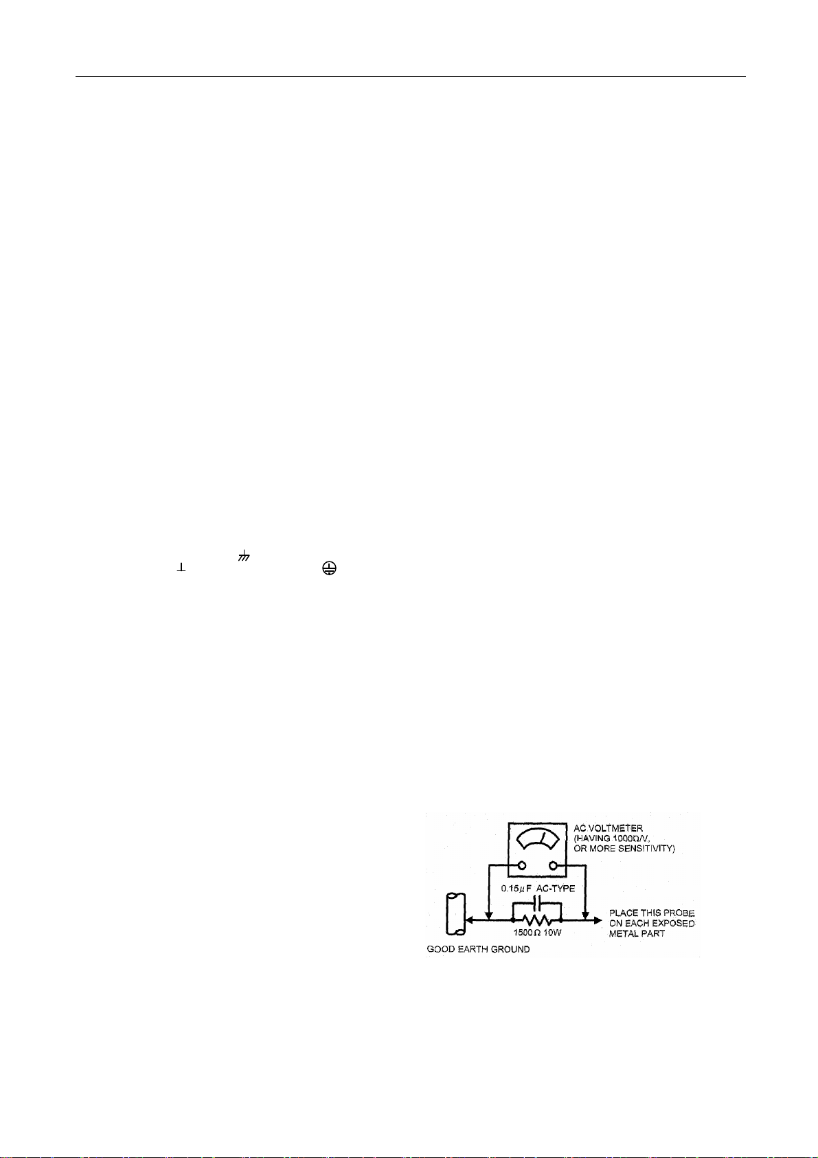
●Alternate Check Method
Plug the AC line cord directly into the AC outlet ( do not use
a line isolation transformer during this check.). Use an AC
voltmeter having 1000 ohms per volt or more sensitivity in
the following manner. Connect a 1500Ω 10W resistor
paralleled by a 0.15μ F AC-type capacitor between an
exposed metal part and a known good earth ground (water
pipe, etc.). Measure the AC voltage across the resistor with
the AC voltmeter. Move the resistor connection to each
exposed metal part, particularly any exposed metal part
having a return path to the chassis, and measure the AC
voltage across the resistor. Now, reverse the plug in the AC
outlet and repeat each measurement. Any voltage
measured must not exceed 0.75V AC (r.m.s.). This
corresponds to 0.5mA AC (r.m.s.).
However, in tropical area, this must not exceed 0.3V AC
(r.m.s.).
This corresponds to 0.2mA AC (r.m.s.)
2
Page 4
2 Block Diagram
TUNER
POWER
UNIT
SAW
+B
+27V
+12V
+8V
+5V
+3.3V
+13V
-13V
EEPROM
V. DRIVE
LA78040
IF1 IN
IF2 IN
RF AGC
SDA
SCL
V OUT
TDA111XX
TDA121XX
SELECT V OUT
AUDIO OUT
E/W
(OPTION)
AR IN
LSL OUT
LSR OUT
RGB OUT
H OUT
V1 IN
V2 IN
Y IN
U IN
V IN
AL IN
C IN
4052
SOUND AMP
AN17821
H. DRIVE
VIDEO AMP
EHT
CRT
V1 IN
AL1 IN
AR1 IN
Y IN
U IN
V IN
V OUT
AL OUT
AR OUT
S-VIDEO
V2 IN
AL2 IN
AR2 IN
SPEAKER L
SPEAKER R
DEFLECT
3
Page 5

3. REPLACEMENT OF MEMORY IC
1. MEMORY IC.
This TV uses memory IC. In the memory IC are memorized data for correctly operating the video and
deflection circuits.
When replacing memory IC, be sure to use IC written with the initial value of data.
2. PROCEDURE FOR REPLACING MEMORY IC
(1) Power off
Switch the power off and unplug the power cord from AC outlet.
(2) Replace IC
Be sure to use memory IC written with the initial data values.
(3) Power On
Plug the power cord into the AC outlet and switch the power On.
4
Page 6

4. SERVICE ADJUSTMENT
4.1 Enter the factory menu
PUSH 【MENU】KEY →DISPLAY PICTURE MANUAL
“B/W BANLANCE”
PRESS【TEST】KEY OR【POWER】WILL BE EXIT FACTORY MODE
IN【TEST】MODE .PRESS【-/--】KEY WILL BE ENTER【BUS OPEN】.
.
PUSH
STANDBY】KEY WILL BE EXIT FACTORY MODE
【
4.2 Enter the adjustment menu
IN “B/W BALANCE” MODE,PRESS【TEST】OR 【CALL】KEY WILL BE ENTER M0.THEN PRESS【MUTE】
KEY WILL ENTER “M1” AND “M2”.
IN “M2” SELECT “SETUP SELECT” TO 1,THEN PRESS【MENU】KEY WILL BE ENTER”M3”
TO ”M9
4.3
CHILD LOCK PASS WORD:[4100]
4.4 Factory MENU
MENU0
M0 PAL NTSC
DESCRIPTION
TEST.SW 0 Internal signal
V.SLOPE 25 +00 Picture vertical center (VARIABLE 0~63)
V.POSI 23 +00 The vertical positions (VARIABLE 0~63)
V.SIZE 32 +00 The vertical amplitude (VARIABLE 0~63)
V.SC 32 +00 The Vertical S-correction (VARIABLE 0~63)
H.PHASE 35 +00 The horizontal position (VARIABLE 0~63)
H.BLK.SW ON Switch of horizontal wide blanking
H.BLK.L 0 Time of horizontal wide blanking start of
blanking((VARIABLE 0~15)
H.BLK.R 0 Time of horizontal wide blanking end of
blanking((VARIABLE 0~15)
PROG 0 external signal
Receive standard Crosshatch pattern signal for PAL system .
Adjust v.slope value to the horizontal line just appear from half bottom shadow.
Adjust V.posi value to the center horizontal line correspond to CRT vertical center
Adjust V.size value to get 90% of vertical picture contents would be displayed on CRT
Adjust VSC value to vertical S-correction is ok
Adjust H.PHASE value to get the picture horizontal center correspond to CRT horizontal
center
PUSH DIGITAL KEY “6483”→ DISPLAY
→
5
Page 7

MENU1
M1 PRESE
DESCRIPTION
T
TEST.S 0 0=external signal,1=black signal , 2=white
signal , 3=red signal , 4=green signal,5=blue
signal
R.BIA 32 R bais adjusted (VARIABLE 0~63)
G.BIA 32 G bais adjusted (VARIABLE 0~63)
B.BIA 32 B bais adjusted (VARIABLE 0~63)
R.DRV 32 R drive adjusted (VARIABLE 0~63)
G.DRV 32 G drive adjusted (VARIABLE 0~63)
B.DRV 32 B drive adjusted (VARIABLE 0~63)
SUB BRT 32 Sub Brightness (VARIABLE 0~63)
VSD Vertical scan disable
CL 12 Cathode drive level(VARIABLE 0~15)
BLOC 6 Black level offset course(VARIABLE 0~15)
SELECT THE SIGNAL IN“TEST.S”MENU
SELECT“VSD” AND PRESS“V+” KEY .WILL BE ENTER SC LINE MODE
PRESS NO.“2”IS REDUCE“R.BIA”AND NO.“3”IS INCREASE“R.BIA”
PRESS NO.“4” IS REDUCE “G.BIA”AND NO.“5” IS INCREASE “G.BIA”
PRESS NO.“6” IS REDUCE “B.BIA” AND NO.“7” IS INCREASE “B.BIA”
WHEN THE WHITE BANLENCE IS OK , AJUST G2 VOLTAGE TO THE SCREEN JUST
DISPLAY THE LINE
PRESS V+ KEY WILL BE EXIT THE SC LINE MODE
MENU2
M2 PRESET
DESCRIPTION
RF.AGC 29 RF AGC (VARIABLE 0~63)
OSD.V.POS 21 16
OSD.H.POS 43 18
Vertical position of OSD(0~63)
Horizital position of OSD(0~15)
OSD BRT 15 Adjust brightness of OSD
SHIPPING Shipping mode
SETUP SELECT 0 The item setup to “1” and press mute
key will be enter next menu
Receive 60dBu (1mv)VH color bar signal,adjust AGC value(voltage from high to low)to
picture noise reduce gradually to be just disappeared. Select “shipping”, push [V+] [V-]key to
be shipped.
6
Page 8

5. IC’s functional description
TDA111XX & TDA121XX
SYMBOL PIN DESCRIPTION
IFVO 1 CVBS output(front-end or selected video)
VP2 2 Supply VSP(IF and sound) --(5V)
VCCAUDIO 3 Supply VSP(only sound output stage)--(8V)
PLLIF 4 IF-PLL time-constant
GND2 5 Ground VSP(IF and sound)
DECSDEM 6 Demodulator decoupling capacitor
FMDEMOUT 7 AVL capacitor,second sound IF output or
EHTO 8 EHT feedback input
AGC 9 Tuner AGC control output
IREF 10 Current reference component
VSC 11 Vertical sawtooth capacitor
IF IN2 12 Video SAW filter input 2
IF IN1 13 Video SAW filter input 2
VDRA 14 Vertical drive output A
VDRB 15 Vertical drive output B
AVL/EW 16 Capacitor for automatic volume leveling or E/W
DECBG 17 Bandgap decoupling
SECPLL 18 SECAM-PLL oscillator
GND1 19 Ground VSP(chroma processing and sync and
PH1LF 20 Acquisition PLL first phase loop
PH2LF 21 Second phase loop components
VP1 22 Supply VSP (5V)
DECDIG 23 Digital decoupling.
XTALOUT 24 24.576MHZ crystal output
XTALIN 25 24.576MHZ crystal input
IR 26 IR receiver
MUTE 27 MUTE output
S-INDENT/UFH 28 S-VIDEO indent
KEY 29 Key input
BAND2 30 BAND 2
BAND1 31 BAND 1
TUNING 32 14 BIT PWM VT output
VDDP 33 Supply TCG periphery(3.3V)
SDA 34
SCL 35
AV1 36 AV1 control
Function : Main IC
demodulated sound output
drive output
geometry)
SDA output
SCL output
7
Page 9

AV2 37 AV2 control
STANDBY 38 Standby output
50/60HZ 39 50/60HZ control
VDDC 40 Supply TCG core (3.3V)
GND5 41 Ground TCG and digital ground VSP
VPE 42 OTP programming voltage
VDDA 43 Analog supply TCG digital supply VSP (3.3V)
BOUT 44 Blue output
GOUT 45 green output
ROUT 46 Red output
BLKIN 47 Feedback input continuous cathode calibration
loop and vertical guard input
BCLIN 48 Average beamcurrent limiter input
PB 49 Pb input
Y3/CVBS3 50 Y CVBS or Y(C)input
PR/C3 51 Cr input
YOUT 52 Y output
YSYNC 53 Input sync separator
VP3 54 Supply VSP(5V)
GND3 55 Ground VSP
HOUT 56 Horizontal deflection line drive output
FBISO 57 Flyback in and sandcastle out
LSR 58 Audio output (loudspeaker right)
LSL 59 Audio output (loudspeaker left)
C2/C3/C4/AIN5R 60 Chroma or audio input
AIN3/IN1R 61 Audio1 input
CVBS2/Y2 62 CVBS2 input
AIN2/1INL 63 AUDIO2 input
CVBS/Y4/AIN5L 64 CVBS1 input
AN17821/17823 Function : audio output
Symbol PIN Function Symbol PIN Function
Vcc 1 Power supply GND 7 ground
Out 1 (+) 2 Ch 1 output (+) In 2 8 Ch 2 input
GND(out 1) 3 Ch 1Ground VOL 9 Volume Control
Out 1 (-) 4 Ch 1 output (-) Out 2 (-) 10 Ch 2 output (-)
Standby 5 Mute input GND(out 2) 11 Ch 2 Ground
In 1 6 Ch 1 input Out 2 (+) 12 Ch 2 output (+)
Note: AN17823 is pin 1 to 9, AN17821 is pin 1 to 12.
8
Page 10

STV9302A /LA78040 Function : vertical output
Symbol PIN Function Symbol PIN Function
INV IN 1 Input V OUT 5 Vertical output
VCC1 2 Power VCC2 6 Output power supply
PUMP UP 3 Pump up power NON INV IN 7 Neg ative feedback
GND 4 Ground
6. Test point Waveforms
2.0Vpp
TDA111XX PIN1
95Vpp 95Vpp
1Vpp
TDA111XX PIN15
TDA111XX PIN24
CRT KG CRT KR
0.8Vpp
T
DA111XX PIN14 HEA
1.2Vpp 1.2Vpp
111XX PIN44
95Vpp
CRT KB
22Vpp
TER
TDA111XX PIN45 TDA111XX PIN46 TDA
0.9Vpp 5Vpp
TDA
111XX PIN56
2.7Vpp
V451 B
1.2Vpp 1.3Vpp
TDA111XX PIN57
1000Vp
V451 C
p
9
Page 11

7. IC’s voltages
TDA111XX/TDA121XX
PIN 1 2 3 4 5 6 7 8 9 10 11 12 13 14 15 16
V 1.5 5 8 2.0 0 2.2 2.6 2.2 1.3 2.0 2.4 1.9 1.9 0.7 0.7 0.4
PIN 17 18 19 20 21 22 23 24 25 26 27 28 29 30 31 32
V 2.3 2.3 0 2.3 1.8 5 2.6 1.8 1.8 5 0 0 3.3 0 0 -
PIN 33 34 35 36 37 38 39 40 41 42 43 44 45 46 47 48
V 3.3 3.8 3.6 0 0 3.3 0 3.3 0 0 3.3 2.2 2.2 2.2 0 2.6
PIN 49 50 51 52 53 54 55 56 57 58 59 60 61 62 63 64
V 0.5 1.4 1.6 1.6 1.9 5 0 0.6 0.35 2.5 2.5 0.6 2.2 1.4 2.2 1.4
STV9302A/LA78040
PIN 1 2 3 4 5 6 7
V 0.7 15 -12 -15 0.3 15.9 -0.07
AN17821/AN17823
PIN 1 2 3 4 5 6 7 8 9 10 11 12
V 12 7 0 7 3.3 1.4 0 1.4 0 7 0 7
10
Page 12

 Loading...