

Page 1
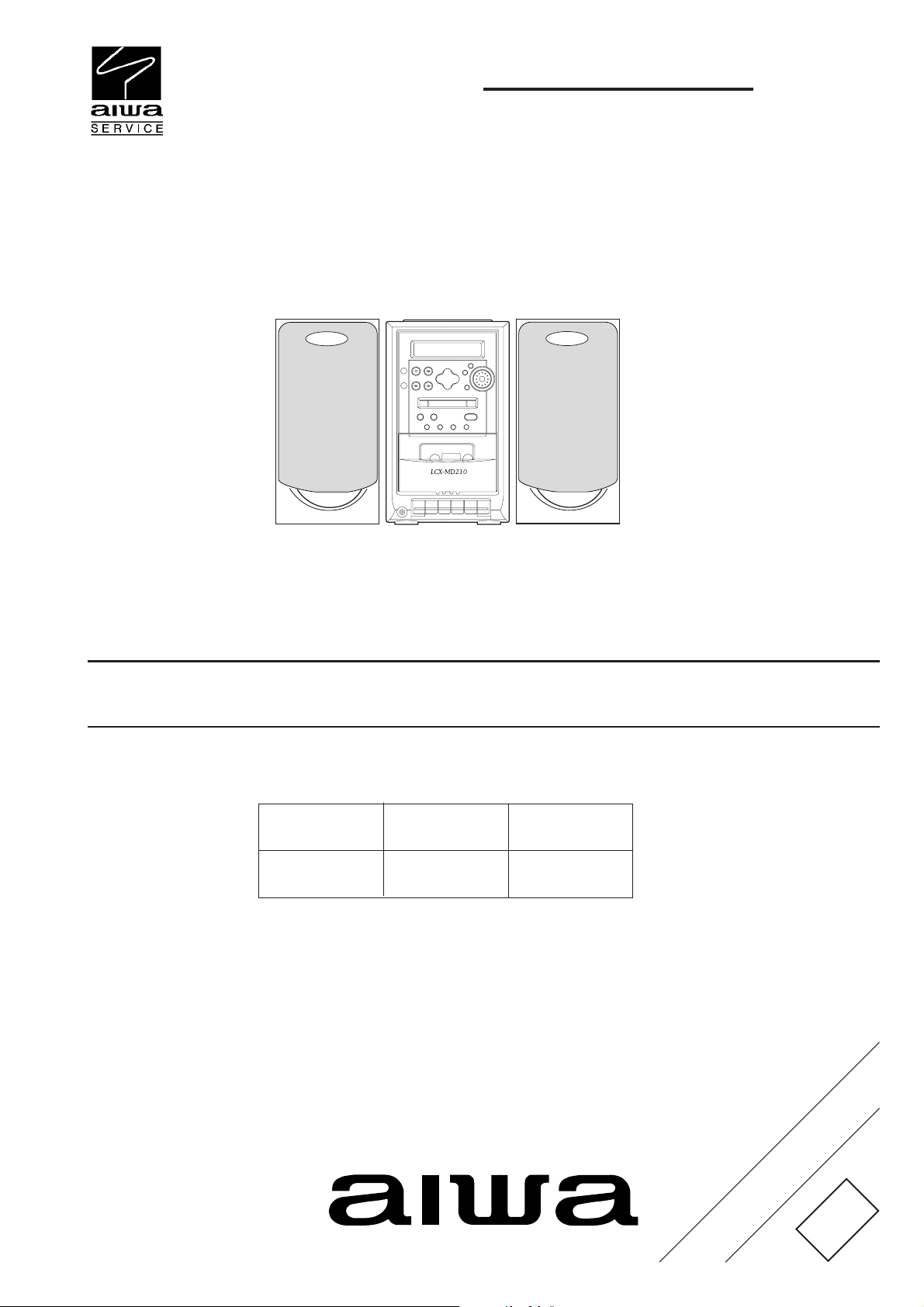
LCX-MD211
EZ
SERVICE MANUAL
MD / CD
STEREO SYSTEM
SYSTEM SPEAKER
LCX–MD211
• This Service Manual contains the additional information “TEST MODE”,
“ADJUSTMENT”, “IC BLOCK DIAGRAM”, “IC DESCRIPTION”,
“LCD DISPLAY” and “VOLTAGE” for the model LCX-MD211(EZ).
If requiring the other information, see Service Manual of LCX-MD211(EZ),
(S/M code No.09-007-429-4R2).
SX-MD210
BASIC TAPE MECHANISM : TN-21ZSC-2003
BASIC CD MECHANISM : DA11T3C
BASIC MD MECHANISM : AZG-4 A
REMOTE
CONTROLLER
RC-AAT11
S/M Code No. 09-00B-429-4S2
SUPPLEMENT
DATA
Page 2
TEST MODE
CD TEST MODE
1-1 How to activate CD Test Mode
Insert the AC plug while pressing the "CD function" button.
Test mode will be activated and [CD TEST] will be appeared in the LCD display.
Note: Test mode can not be activated when CD door switch is opened.
1-2 CD Test Mode Functions
Mode
Start Mode
Search Mode
Play Mode PLAY
Traverse Mode TRAVERS
Sled Mode
* Note 1: There are cases when CD cannot be operated owing to the protection circuit being operated when heat builds up in the driver IC if the
focus search is operated continually for more than 10 minutes. In this case, the power supply should be switched off for ten minutes
until heat has been reduced and then re-start.
1-3 How to cancel CD Test Mode
Either one of the following operations will cancel the CD test mode.
• Open the CD door switch.
• Press "POWER" button.
• Disconnect the AC plug.
Function
Activate CD
Test Mode
s
E
Tuner Function
Button
g
f
Display
CD TEST
SEARCH
SLED IN
SLED OUT
Operation Content
•
Continuous Focus Search (Pickup lens
repeat full swing)
* Note 1
• Normal Playback
When TOC READ is unavailable,
•
continuous Focus Search (Same as
Search Mode Operation)
Playback pause status Tracking servo OFF
Shift to the internal circumference of
•
pickup
• Shft to the external circumference of
pickup
APC circuit check
Laser current measurement
•
Focus error waveform check
•
•
Focus servo
Tracking servo
•
CLV servo
•
Sled servo
•
•
Sled servo
Mecha operation check
•
LCD TEST MODE
1-1 How to activate LCD Test Mode
Insert the AC plug while pressing the "DISPLAY" button.
LCD display is fully illuminated and then all segments are lit on and off every one second.
1-2 How to cancel LCD Test Mode
LCD test mode will cancel by press "POWER" button or disconnect the plug.
– 2 –
Page 3
MD TEST MODE
1-1 How to start up MD Test Mode
Insert the AC plug while pressing the "MD function" button.
After the MD test mode has started up, [MD TEST] message appears and the test mode becomes operatable.
Note: • Disconnect the AC plug immediately if any mechanism abnormalities.
• Playback and recording are not possible during the test mode.
1-2 How to cancel MD Test Mode
1) Press the "MD EJECT" button and remove the disc.
2) Disconnect the AC plug or press "POWER" button.
1-3 Operation Check Mode
1) Checks after the test mode has started up.
The following playback audio circuits can be checked.
• Enable circuit to check ------------ DAC, LINEAMP, HEADPHONE AMP
• Output level ------------------------- 1KHz, -24dB
2) Switch status check
ON/OFF statuses of main unit and mechanism switches can be checked on display.
Switch name Indication on Display Usalde disc
REC PROTECT
REFRECT
INNER
1-4 How to switch to Servo Standby Mode
When the test mode has been established, the mode changes to the servo standby mode by pressing "s" button (lndication on display : ALL
SVOFF).
The various check modes can be entered from this mode.
Pressing the "s" button during each operation returns to [ALL SVOFF].
1-5 Checking Sled Operation
1) When "g" button is pressed in the [ALL SVOFF] state, pickup moves in the outer direction. [T SLEDFWD] is displayed.
2) When "g" button is pressed in the [ALL SVOFF] state, pickup moves in the inner direction. [T SLEDRVS] is displayed.
1-6 Checking Laser Power
1) The laser power is switched each time the "EDIT" button is pressed in the "ALL SVOFF" state. Laser power output is changed as
OFF
bLASER READbLASER 1/2bLASER WRITEbOFF order and indication on the display is follows;
When the write-protection tab of disc is
stopped.
When the high reflection disc (CD) is
used.
When the pickup is the positioned at the
innermost track (when the LIMIT SW is
ON).
Switch state
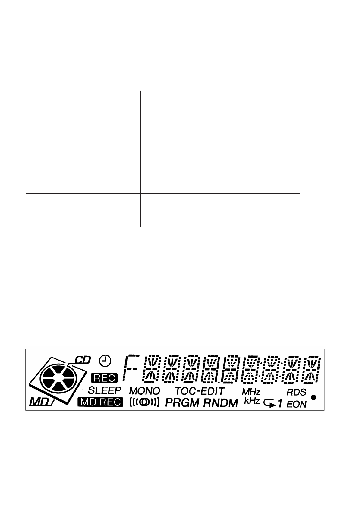
TOC – EDIT
MD REC
MONO
Record/playback disc
Playback only disc
Mode
OFF
LASER READ
LASER 1/2 WRITE
LASER WRITE
2) Press "s" button to return the display to [ALL SVOFF] after checking.
1-7 Checking OWH (Over Write Head) Operation
The operation of OWH can be checked by pressing following buttons in the loading status.
"MD EJECT" button-----------------------OWH UP
"SYNCHRO REC" button----------------OWH DOWN
* Note: Do not down OWH when using the high reflection disc (CD).
1-8 Checking Servo Operation
• Checking the focus search and spindle kick 1
1) When "E" button is pressed in the [ALL SVOFF] state without disc, focus search and spindle kick are executed continuously.
[ FOCUS SCH] is displayed.
Indication on display
ALL SVOFF
LA READ
LA 1/2
LA WRITE
– 3 –
Page 4

2) Press "s" button to display [ALL SVOFF] after checking
• Checking the focus search and spendle kick 2
1) When "TUNER function" button is pressed in the "ALL SVOFF" state regardless disc existence, focus search and spindle kick are executed
continuously. [FOCUS CHK] is displayed and S curve can be checked if disc is loaded.
2) Press "s" button to display [ALL SVOFF] after checking.
• Checking Focus Servo
1) Insert a test disc.
2) Move pickup to center track by pressing "g" or "f" buttons.
3) Press "JOG MODE" button to set the servo mode according to the inserted disc as follows;
• MO disc (MO)----------------Indication on display [SEL GRV].
• PIT disc (CD)-----------------Indication on display [SEL PIT].
4) Press "E" button.
If focus servo is operating normally, the messge [FOCUS ON] is displayed after [FOCUS SCH].
5) Press "s" button to display [ALL SVOFF] after checking.
• Checking all Servos are turned on.
1) Tracking and sled servos and turned on and all servos work when "ENTER" button is pressed in the [FOCUS ON!] state. [ALL SV ON] is
displayed if all servos are normal.
2) Press "s" button to display [ALL SVOFF] after checking.
– 4 –
Page 5
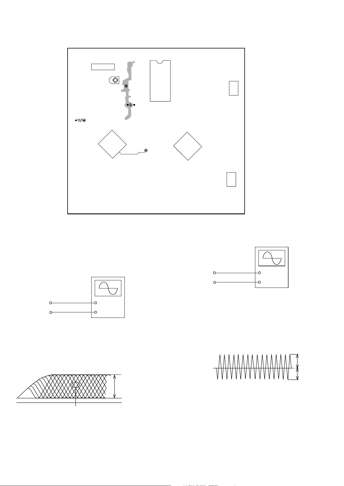
ADJUSTMENT <TUNER / DECK>
A
MAIN C.B
L771
IC771
TP5
J201
L772
2826
TP6
FFE801
L942
TC942
TP7(Rch)
C785
C786
TP8(Lch)
+
+
IC201
IC202
TP4 (VT)
1
4
L981
IC721
L941
< TUNER SECTION >
1. MW VT Check
Settings : • Test point : TP4 (VT)
Method : Set to MW 1602kHz and check that the test point is
less than 5.6V.
2. MW Tracking Adjustment
Settings : • Test point : TP7 (RCH), TP8 (LCH)
• Adjustment location : L981
Method : Set to MW 999kHz and adjust L981so that the test
point becomes maximum.
3. AM IF Adjustment
Settings : • Test point : TP7 (RCH), TP8 (LCH)
• Adjustment location:
L772 .................................................... 450kHz
4. LW VT Adjustment
Settings : • Test point : TP4 (VT)
• Adjustment location : L942
Method : Set to LW 153kHz and adjust L942 so that the test
point becomes 1.3V ± 0.05V.
5. LW Tracking Adjustment
Settings : • Test point : TP7 (RCH), TP8 (LCH)
• Adjustment location :
L941 .................................................... 153kHz
TC942 .................................................. 285kHz
Method : Set up TC942 to center before adjustment. The level at
153kHz is adjusted to maxinum by L941. Then the
level at 285kHz is adjusted to maxinum by TC942.
6. FM VT Check
Settings : • Test point : TP4 (VT)
Method : Set to FM 108MHz and check that the test point is less
than 8.2V .Then set to FM 87.5MHz and check that
the test poit is more than 1.5V.
7. FM Tracking Check
Settings : • Test point : TP7 (RCH), TP8 (LCH)
Method : Set to FM 98MHz and check that the test point is less
than 18dB.
8. DC Balance / Mono Distortion Adjustment
Settings : • Test point : TP5, TP6 (DC balance)
TP7 (RCH), TP8(LCH)(Distortion)
• Adjustment location : L771
• Input level : 54dB
Method : Set to FM 98MHz and adjust L771 so that the voltage
between TP3 and TP4 becomes 0V ± 0.04V.
Next, check that the distortion is less than 1.5%.
9. FM Separation Check
Settings : • Test point : PHONE JACK (J201)
• Input level : 54dB
Method : Set to FM 98MHz and check that the test point is more
than 20dB.
< DECK SECTION >
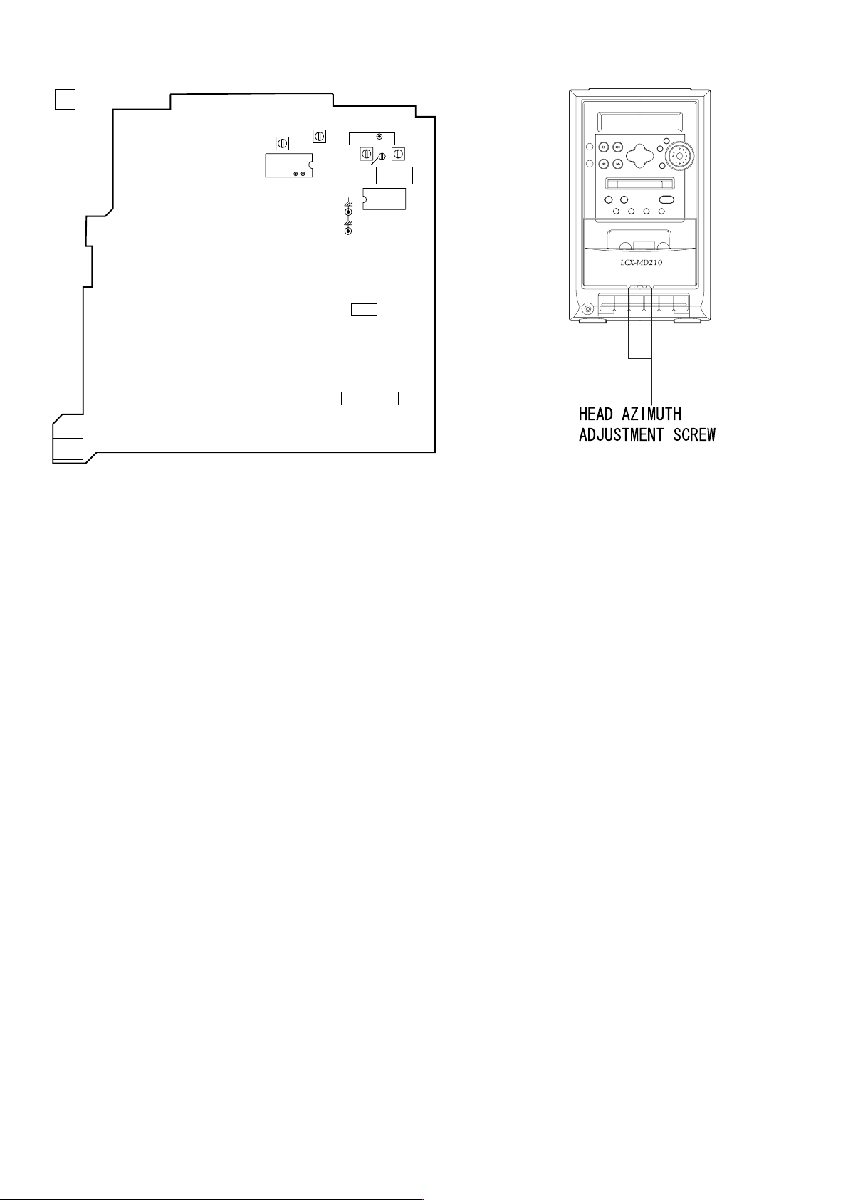
10. Head Azimuth Adjustment
Settings : • Test tape : TTA–330
• Test point : PHONE JACK (J201)
• Adjustment location : Head azimuth
adjustment screw
Method : 1) Connect the L positive terminal to CH1 probe
(positive side) of oscilloscope and L negative
terminal to CH1 probe (negative side).
Connect the R positive and negative terminals to
CH2 probe same condition as CH1 probe.
2) Play back the 10kHz signal of the test tape.
3) Adjust the head azimuth adjustment screw to
become maximum waveform in the oscilloscope
and same phase for CH1 and CH2.
– 5 –
Page 6
<CD>
CD C.B
CN401
SFR430
TP
(VREF)
C431
+
TP(TE)
R405
41
IC401
Note: • Connect a provbe (10 : 1) of the oscilloscope to adjust.
• Connect negative side of the oscilloscope to TP (VREF) for
each adjustment.
1. Focus Bias Adjustment
Adjust focus bias when replaing or repairing the optical block.
TP(RFSM)
IC404
CN405
IC402
CN403
2. Tracking Balance Adjustment
Oscilloscope
(DC range)
Oscilloscope
(DC range)
TP (RFSM)
TP (VREF)
1) Connect an oscilloscope to the test points TP (RFSM) and
TP(VREF).
2) Turn on the "POWER" button.
3) Insert the test disc TCD-782 (YEDS-18) and playack the 2nd
composition.
4) Adjust SFR430 so that RF signal of the test point is MAX and
CLEARREST.
EYE PATTERN
must be CLEAR and MAX
+
_
Max
VOLT/DIV: 0.5V
TIME/DIV: 0.5uS
TP (TE)
TP (VREF)
1) Connect an oscilloscope to the test point TP (TE) and
TP (VREF).
2) Active the CD test mode.
3) Insert the test disc TCD-782 (YEDS-18) and choose traverse
mode of CD test mode.
4) Check that the waveform of traverse is vertically symmetrical as
shown below.
5) Cancel CD test mode after checking.
VREF
+
_
A
B
A=B
VOLT/DIV: 20mV
TIME/DIV: 1mS
– 6 –
Page 7

<MD>
• Perform 1~3 adjustment when display showing [NO ADJUST].
1. Temperature Compensation Adjustment
• Test point: Check on the display.
• Tool : Thermometer
• Adjustment procedure
1) After MD test mode has started up, press "s" button to display
[ALL SVOFF].
2) Press "DISPLAY" button to display [TEMP = ].
3) Press "T-BASS" button to display [T + ** C ± ##].
4) Put the thermometer near the MD mechanism to measure the
room temperature.
5) Adjust the indication value ** using "l" and "j" buttons until
the value is the same as room temperature.
Press "ENTER" button after adjusting.
6) Ptess "s" button to display [ALL SVOFF] after adjusting.
7) After adjustment is completed, once again set the display to
[TMP + ** C ± ##] and check the value that has been
caluculated with the addition or subtraction of the numerical
values of ## in relation to the ** value. This value is to be the
same sa room temperature.
NOTE: Do not perform this adjustment if it is not possible to
measure the room temperature.
S
S
Then, confirm the values of [I ** E ] in the display are
within the following range.
[ ** ] ......................... 04~0A
[ ] ......................... 09~15
S
S
5) Press "DISPLAY" button again.
Confirm the values of [F ** T ## S II ] in the display are
within the following range.
[**] ........................... 1A~45
[##] ........................... 00~03
[II ] ........................ 00~03
6) Press "s" button to display [ALL SVOFF].
Adjustment for PIT disc
1) Insert the TGYS-1 test disc.
2) Press "s" button to display [ALL SVOFF].
3) Press "JOG MODE" button to display [SEL PIT].
4) When pressing "MD function" button, [AUTO ADJ] is
displayed and adjustment start.
After adjusting, [DONE] is displayed.
(If [failed] is displayed, the adjustment failed.)
5) Press "s" button to display [ALL SVOFF].
S
S
2. Laser Power Adjustment
• Test point: Pickup laser output
• Tool : Laser power meter
• Adjustment procedure
1) Starting in the [ALL SVOFF] status, press "EDIT" button three
times to change the display to [LA WRITE].
2) Press "T-BASS" button once and change the display to
[LASER = **].
3) Measure the laser output of pickup with the laser power meter
and adjust output by "g" or "f" buttons so that the
measurement value becomes 6.8mW ± 0.03mW.
Press "ENTER" button after adjusting.
4) Press "s" button to display [ALL SVOFF] after adjusting.
Caution: There is a possibility that pickup may be damaged if
laser output exceeds 7.0mW.
3.Auto Sequence Adjustment (EFB/IVR/FOCUS AGC/TRACKING
AGC adjustment)
• Test disc: MDW-60, TGYS-1
Adjustment MO disc
1) Insert the MDW-60 test disc.
2) Press "s" button to display [ALL SVOFF].
3) Press "JOG MODE" button to display [SEL GRV].
4) When pressing "MD function" button, [AUTO ADJ] is
displayed and adjustment start.
After adjusting, [DONE] is displayed.
(If [FAILED] is displayed, the adjustment failed.)
5) Press "s" button to display [ALL SVOFF].
NOTE: 1.As there is a posibility that adjustment may not be
able to adequately performed if the disc is dirty or
scratched, make sure to keep the disc clean.
2.When using a MO disc, one section will be erased in
order to change it to WRITE POWER, so a special
disc is to be used.
Checking for IVR, EFB and focus/tracking/sled gain of MO disc
1) Move the pickup to the center track using "g" or "f"
buttons.
2) Press "E" button to display [FOCUS ON].
3) Press "ENTER" button to switch the mode to [ALL SV ON].
4) Press "s" button and "DISPLAY" button twice.
Checking IVR, EFB and focus/tracking/sled gain of PIT disc
Perform the same procedures as for MO disc and check that the
display is within the range below;
[IVR]..............................14~19
[EFB]..............................09~15
[FOCUS GAIN].............1A~45
[Tracking gain]...............00~3F
[Sled gain]......................00~3F
4. Checking Error Rate (PIT disc)
1) Insert the TGYS-1 test disc.
2) Move the pickup to the center track using "g" or "f"
buttons.
3) Press "JOG MODE" button to display [SEL PIT].
4) Press "E" button to display [FOCUS ON].
5) Press "ENTER" button to switch the mode to [AL SV ON].
Then press "DISPLAY" button twice to display [00 ** 000].
6) Check the value of ** is below [30] at this time.
7) Press "s" button to display [ALL SVOFF].
5. Checking Record/Playback Error Rate (MO disc)
1) Insert the MDW-60 test disc.
2) Move the pickup to the center track using "g" or "f"
buttons.
3) Press "JOG MODE" button to display [SEL GRV].
4) Press "MD REC" button to display [R ANALOG].
5) Press "E" button to display [FOCUS ON].
6) After displaying [ALL SV ON] by pressing "ENTER" button,
press "SYNCRO REC" button.
7) Recording begins after OWH has moved when "MD REC"
button is pressed once again.
At this time, display will change from [ALL SV ON] to
[A0600C ## S].
8) Press "s" button after recording has progressed for about 15
seconds, changing the display to [ALL SVOFF].
9) Press "MD EJECT" button to raise the OWH.
10) Press "E" button to display [FOCUS ON].
11) Once [ALL SV ON] has been displayed by pressing "ENTER"
button, press "DISPLAY" button to display [A
After
to display [00 // 000].
Check that the value of // is below than [20] at this time.
reaching 600, press "DISPLAY" button once again
****
****
C ## S].
– 7 –
Page 8

12) Press "s" button to display [ALL SVOFF].
6. UTOC ERASE
To be performed only when erasure is needed with disc that have
already been recorded upon.
1) Insert the disc that is to be used to erase the UTOC.
2) Move the pickup to the center track using "g" or "f"
buttons.
3) Press "JOG MODE" button to display [SEL GRV].
4) Press "MD REC" button to display [R ANALOG].
5) Press "E" button to display [FOCUS ON].
6) Press "ENTER" button to display [ALL SV ON].
7) Press "MD REC" button for move than one second continuously,
[UTOC ERASE] will be displayed and UTOC erased.
8) Once the UTOC has been erased, [ALL SVOFF] will be
displayed.
– 8 –
Page 9

SERVICE JIG AND TOOLS
Service jigs and tools for repairing as follows;
CD
CD mecha stand
PU extention FFC
MD
LCD DISPLAY
GRID ASSIGNMENT
Usage
S.T.I. G-98-50
S.T.I. G-98-50
Parts Name Parts No
JIG, P-CD BY TORIKOSHI
FFC-CABLE, 16P 1.0 250mm
FFC, 8P-1.0
FFC, 14P-1.0
SV-J00-018-010
87-CE1-640-010
SV-J00-043-010
SV-J00-044-010
ANODE CONNECTION
oN 123456789 011121314151
1MOC------1MOCa1i1h1f1a2i2h21LOCa3i3h3
2MOC----2MOC--b1j1g1e1b2j2g2f2b3j3g3
3MOC--3MOC----c1k1n1d1c2k2n2e2c3k3n3
4MOC4MOC------1Pl1m1NOESDRl2m2d2"1"l3m3
oN617181910212223242526272829203
1MOCf3--a4i4h4f4a5i5h5f5a6i6h6f6a7
2MOCe32LOCb4j4g4e4b5j5g5e5b6j6g6e6b7
3MOCd3zHMc4k4n4d4c5k5n5d5c6k6n6d6c7
4MOCPRzHk--l4m4--3Pl5m5
MDNR
2Pl6m6MGRP
COT
TIDE
9
Page 10

oN13233343536373839304142434
1MOCi7h7f7a8i8h8f8a9i9h9f91DM
2MOCj7g7e7b8j8g8e8b9j9g9e91T
3MOCk7n7d7c8k8n8d8c9k9n9d91DC2DC
4MOCl7m7
DM
CER
ONOM
l8m8PEELSCERl9m9012DM
6D,3D
5D,2D
4D,1D
10
Page 11

IC DESCRIPTION
IC, LC877264A-EZ
Pin No. Pin Name I/O Description
1 O-ARDY O Output ready signal for MD micro controller communication. L: Enable.
2 O-SREQ O Request system micro controller output for MD micro controller communication. L: Enable.
3 O-SOUT O Output serial data for MD micro controller communication.
4 I-SIN I Input serial data for MD micro controller communication.
5 I-ACLK I Input serial clock for MD micro controller communication.
6 I-MREQ I Request system micro controller output for MD micro-computer communication. L: Enable.
7 NC (SELECT) - Not used.
8 O-PCONT O Output system power control. H: ON.
9 I-HOLD I Detect Hold status. L: HOLD.
10 O-CLKSFT O Control clock shift. L: Shift.
11 I-RESET I Input reset.
12 XT1 I Not used (pull up in VDD).
13 XT2 - Not connected.
14 VSS1 - Power supply (-) terminal.
15 CF1 I Input terminal for ceramic oscillator (5.76MHz).
16 CF2 O Output terminal for ceramic oscillator (5.76MHz).
17 VDD1 - Power supply (+) terminal.
18 I-JOGA I Detect jog dial A.
19 I-JOGB I Detect jog dial B.
20 I-KEY1
21 I-KEY2
22 I-RDSIG I Input RDS signal level and AD.
23 I-CTON I Detect CT deck power. H: OFF, L: ON.
24 I-RDDT I Input RDS data.
25 I-COLOR I Input LCD back light initial setting.
26 I-TMBASE I Input reference frequency for 8Hz clock.
27 I-INIT I Input diode matrix initial setting.
28 I-RDCL I Input RDS clock.
29 I-RMC I Input received singnal for remote controller.
30 I-CTPLAY I Detect CT deck play. H: PLAY.
31 I-CTREC I Detect CT deck record. H: REC.
32 O-TUCONT O Control tuner power. H: ON.
33 O-TUCE O Output chip enable for tuner PLL communication.
I Detect tact key AD input.
34 O-TUDI O Output serial data for tuner PLL communication.
35 O-TUCL O Output clock for tuner PLL communication.
36 I-TUDO I Input serial data for tuner PLL communication.
37 I-STEREO I Detect receiving tuner stereo. H: MONO, L: STEREO.
38 NC - Not connected.
39~53 S9~S23 O Output LCD segment.
54 VDD2 - Power supply (+) terminal.
55 VCC2 - Power supply (-) terminal.
56~79 S24~S47 O Output LCD segment.
– 11 –
Page 12

Pin No. Pin Name I/O Description
80 I-DOOR I Detect CD door. H: OPEN, L: CLOSE.
81 I-WRQ I Sub code Q read standby for CD LSI communication.
82 I-DRF I Input RF level detection.
83 COM0 O Output COM1.
84 COM1 O Output COM2.
85 COM2 O Output COM3.
86 COM3 O Output COM4.
87 O-CDCONT O Control CD power. H: ON.
88 I-SQOUT I Input sub code Q for CD LSI communication
89 VSS3 – Power supply (-) terminal.
90 VDD3 – Power supply (+) terminal.
91 O-RWC O Input/output switching control for CD LSI communication. H: Write, L: Read.
92 O-COIN O Output serial data for CD LSI communication.
93 O-CQCK O Output serial clock for CD LSI communication.
94 O-LIGHT1 O Output LCD back light control 1.
95 O-JOGLED O Indicate the JOG function status. L: Volume.
96 O-SCONTM O Control sound processor. H: H, M: H, L: L.
97 O-SCONTL O Control sound processor. H: H, M: L, L: L.
98 O-MUTE O Output audio signal mute. H: ON.
99 O-LIGHT2 O Output LCD back light cotrol 2.
100 O-SRST O Reset MD micro controller. L: Reset.
– 12 –
Page 13

IC, LA9241ML
Pin No. Pin Name I/O Description
1 FIN2 I
2 FIN1 I Connect to the pickup's photo diode.
3 E I Connect to the pickup's photo diode; subtracting this pin from pin F generates TE signal.
4 F I Connect to the pickup's photo diode.
5 TB I Input for DC component of TE signal.
6 TE– I Connect to the resistor between this pin and TE pin for setting the gain of TE signal.
7 TE O Output for TE signal.
8 TESI I Input for TES (Track Error Sense) comparator, TE signal is band-passed and inputted.
9 SCI I Input for shock detection.
10 TH I For setting tracking gain time constant.
11 TA O TA amplifier output pin.
12 TD– I For constructing tracking phase compensation constant between TD and VR pins.
13 TD O For setting tracking phase compensation.
14 JP I For setting the amplifier of tracking jump signal (kick pulse).
15 TO O Output for tracking control signal.
16 FD O Output for focusing control signal.
17 FD– I For constructing focusing phase compensation constant between FD and FA pins.
Connect to the pickup's photo diode; adding this pin to pin FIN1 generates RF signal,
and subtracting it generates FE signal.
18 FA O For constructing focusing phase compensation constant between FD– and FA– pins.
19 FA– I For constructing focusing phase compensation constant between FA and FE pins.
20 FE O Output for FE signal.
21 FE– I Connect to the gain-setting resistor of FE signal between this pin and FE pin.
22 AGND – GND for analog signals.
23 SP O Single end output of CV+ and CV– pin input signal.
24 SPI I Input spindle amplifier.
25 SPG I Connect to the gain-setting resistor during spindle 12cm mode. (Not connected)
26 SP– I Connect to spindle phase compensation constant together with SPD pin.
27 SPD O Output for spindle control signal.
28 SLEQ I Connect to sled phase compensation constant.
29 SLD O Output for sled control signal.
30 SL–
31 SL+
32 JP–
33 JP+
34 TGL I Input for tracking gain control signal from DSP; gain is low if TGL = "H".
35 TOFF I Input for tracking off control signal from DSP; off if TOFF = "H".
I Input for sled-sending signal from microcontroller.
I Input for tracking jump signal from DSP.
36 TES O Output TES signal to DSP.
37 HFL O
38 SLOF I Input for sled servo off control.
HIGH FREQUENCY LEVEL; used to determine whether the main beam is on a pit or
on a mirror.
– 13 –
Page 14

Pin No. Pin Name I/O Description
39 CV–
40 CV+
41 RFSM O Output for RF.
42 RFS– O For setting RF gain and 3T compensation constant together with RFSM.
I Input for CLV error signal from DSP.
43 SLC O
44 SLI I Input for controlling the data slice level of DSP.
45 DGND – GND for digital system.
46 FSC O Output pin for focus search smoothing capacitor.
47 TBC I (Tracking Balance Control) EF balance variable range setting pin.
48 NC – Not connected.
49 DEF O Output for disk defect detection.
50 CLK I Reference clock input; DSP's 4.23MHz is inputted.
51 CL I Clock input for micro controller command.
52 DAT I Data input for micro controller command.
53 CE I Chip-enable input for micro controller command.
54 DRF O Detect RF; output for RF level detection.
55 FSS I (Focus Search Mode) = search/+search against reference voltage switching pin. (Not connected)
56 VCC2 – VCC pin for servo and digital systems.
57 REFI – For connecting pass capacitor to reference voltage.
58 VR O Reference voltage output.
59 LF2 – For setting disk defect-detection time constant.
60 PHI – Connect to capacitor for RF signal peak hold.
SLICE LEVEL CONTROL; output for controlling the data slice level of DSP with
RF waveform.
61 BHI – Connect to capacitor for RF signal bottom hold.
62 LDD O Output for APC circuit.
63 LDS I Input for APC circuit.
64 VCC1 – VCC pin for RF system.
– 14 –
Page 15

IC, LC78622ED
Pin No. Pin Name I/O Description
1 DEFI I Defect detection signal (DEF) input.
2 TAI I Test input. A pull-down resistor is built in. (Must be connected to 0V)
3 PDO O External VCO control phase comparator output.
4 VVSS – Internal VCO ground. (Must be connected to 0V)
5 ISET I PDO output current adjustment resistor connection.
6 VVDD – Internal VCO power supply.
7 FR I VCO frequency range adjustment.
8 VSS – Digital system ground. (Must be connected to 0V)
9 EFMO O Slice level control; EFM signal output.
10 EFMIN I Slice level control; EFM signal input.
11 T2 I Test input. A pull-down resistor is built in. (Must be connected to 0V)
12 CLV+
O
13 CLV–
14 V/P O Rough servo/phase control automatic switching monitor output. H: Rough servo, L:phase servo.
15 HFL I Track detection signal input. This is a Schmitt input.
16 TES I Tracking error signal input. This is a Schmitt input.
Disc motor control output.
Three-value ouput is also possible when specified by microprocessor command.
17 TOFF O Tracking off output.
18 TGL O Tracking gain switching output. Increase the gain when low.
19 JP+ O Track jump output.
20 JP– Three-value output is also possible when specified by microprocessor command.
21 PCK O
22 FSEQ O detected from the EFM signal and the internally generated synchronization signal agree.
23 VDD – Digital system power supply.
24 SL+ O Sled advance + signal output.
25 SL– O Sled advance - signal output.
26 NC – Not connected.
27 PU IN I CD pickup inside limit switch. When inside limit input "L", when CD-RW output "H".
28 RW O Gain control.
29 EMPH O De-emphasis monitor pin. De-emphasis disc is being played back at H. (Not connected)
30 C2F O C2 flag output. (Not connected)
31 DOUT O Digital output (EIAJ format).
32 T3
I Test input. A pull-down resistor is built in. (Must be connected to 0V)
33 T4
EFM data playback clock monitor. Outputs 4.3218 MHz when the phase is locked.
(Not connected)
Synchronization signal detection ouput. Outputs a high level when the synchronization signal
(Not connected)
34 NC – Not connected.
35 MUTEL O Left channel one-bit DAC L channel mute output. (Not connected)
36 LVDD – Left channel one-bit DAC L channel power supply.
37 LCHO O Left channel one-bit DAC L channel output.
38 LVSS – Left channel one-bit DAC L channel ground. (Must be connected to 0V)
– 15 –
Page 16

Pin No. Pin Name I/O Description
39 RVSS – Right channel one-bit DAC R channel ground. (Must be connected to 0V)
40 RCHO O Right channel one-bit DAC R channel output.
41 RVDD – Right channel one-bit DAC R channel power supply.
42 MUTER O Right channel one-bit DAC R channel mute ouput. (Not connected)
43 XVDD – Crystal oscillator power supply.
44 XOUT O
45 XIN I
46 XVSS – Crystal oscillator ground. (Must be connected to 0V)
47 SBSY O Subcode block synchronization signal output. (Not connected)
48 EFLG O C1, C2 single and double error correction monitor pin. (Must be connected to 0V)
49 PW O Subcode P, Q, R, S, T, U, V and W output. (Not connected)
Connection for a 16.934MHz crystal oscillator element.
50 SFSY O
51 SBCK I Subcode readout clock input. This is a Schmitt input. (Must be connected to 0V)
52 FSX O
53 WRQ O Subcode Q output standby output.
54 RWC I Read/write control input. This is a Schmitt input.
55 SQOUT O Subcode Q output.
56 COIN I Command input from the control microprocessor.
57 CQCK I
58 RES I Reset pin. This pin must be set low briefly after power is first applied.
59 T11 O Test output. Leave open. (Normally outputs a low level). (Not connected)
60 16M O 16.9344 MHz output. (Not connected)
61 4.2M O 4.2336 MHz output.
62 T5 I Test input. A pull-down resistor is built in. (Must be connected to 0V)
63 CS I Chip select input. A pull-down resistor is built in. (Must be connected to 0V)
64 T1 I Test input. No pull-down resistor. (Must be connected to 0V)
Subcode frame synchronization signal output. This signal falls when the subcode are in the
standby state. (Not connected)
Output for the 7.35 kHz synchronization signal divided from the crystal oscillator.
(Not connected)
Command input read clock or subcode readout input clock from SQOUT pin.
This is a Schmit input
– 16 –
Page 17

IC, LC72131D
Pin No. Pin Name I/O Description
1 X IN I A crystal oscillator (4.5MHz) is connected to X OUT pin.
2 NC – Not connected.
3 CE I To enable the IC. Active "H".
4DII
5 CL I To clock in the data DI.
6 DO O Digital data output to CPU (LC877264A-EZ).
7 T-BASE O Output a reference clock signal (8Hz) for the clock.
8 MONO / BEAT O Output "L" when MONO / BEAT is switched.
9 FM / SW O
10 MW / SW O
11 IF-MUTE O To control internal counter.
12 IF-IN I General purpose counter input.
13 TUNE I Receives "L" when station is tuned.
14 NC – Not connected.
15 AMIN I Receives the AM local oscillator frequency signal.
Digital data input from CPU (LC877264A-EZ) when relevant key is operated.
Active "H".
Output "L" or "H" as follows:
2 BAND 3 BAND
AM FM LW MW FM
HLHHL
Output "L" or "H" as follows:
2 BAND 3 BAND
AM FM LW MW FM
LLHLL
16 FMIN I Receives the FM local oscillator frequency signal.
17 VDD – Supply power to IC (+5V).
18 PD O PLL charge pump output.
19 AIN I
20 AOUT O
21 VSS – Ground.
22 X OUT O A crystal oscillator (4.5MHz) is connected to X IN pin.
The MOS transistor used for PLL active low pass filter.
– 17 –
Page 18

IC BLOCK DIAGRAM
- 18 -
Page 19

- 19 -
Page 20

VOLTAGE CHART
< CD > Test condition : CD play
IC401(LA9241ML)
IC402(LC78622ED)
1 2.5
2 2.5
3 2.5
4 2.5
5 2.5
6 2.5
7 2.5
8 2.5
9 2.5
10 2.5
11 2.5
12 2.5
13 2.4
14 2.5
15 2.5
16 2.5
17 2.5
18 2.5
41 2.3
42 2.4
43 2.6
44 2.5
45 0
46 2.5
47 2.5
48 0
49 0
50 2.5
51 4.3
52 5.1
53 0
54 4.8
55 0
56 5.0
57 2.5
58 2.5
10
20
3 1.5
40
5 1.9
6 5.0
7 0.3
80
9 2.5
10 2.6
11 0
12 0.2
13 0
14 0
15 0
16 1.6
17 0
18 5.0
41 4.8
42 0
43 5.0
44 2.1
45 2.1
46 0
47 0.1
48 0
49 0.1
50 2.5
51 0
52 2.5
53 1.6
54 0
55 0.3
56 5.1
57 4.3
58 5.0
19 2.5
20 2.5
21 2.5
22 0
23 2.5
24 2.5
25 2.5
26 2.5
27 2.6
28 2.5
29 2.6
30 2.3
31 2.3
32 0
33 0
34 5.0
35 0
36 1.6
59 2.4
60 2.4
61 2.2
62 3.7
63 0.2
645.0
19 0
20 0
21 2.5
22 5.0
23 5.0
24 0
25 0
26 5.0
27 5.0
28 0
29 0
30 0
31 2.4
32 0
33 0
34 0
35 0
36 4.8
59 0
60 2.5
61 2.4
62 0
63 0
64 0
37 0
38 0
39 0
40 0.2
37 2.1
38 0
39 0
40 2.1
20
Page 21

< CD >
IC403(LA6541D)
< TUNER > Test condition : Tuner function
IC721(LC72131D)
IC771(LA1837N)
1 7.8
2 5.0
30
4 2.5
5 3.5
6 3.5
70
80
90
10 3.5
11 3.5
12 2.5
13 2.5
14 5.0
15 7.1
16 5.0
17 4.9
18 2.5
AM FM
1 2.6 2.5
200
300
400
500
6 5.2 2.4
7 2.5 2.5
8 0 8.0
9 8.0 0
10 0 0
11 0 0
12 0 0
13 7.9 2.5
14 0 0
15 2.6 0
16 0 2.6
17 5.3 5.2
AM FM
1 3.6 3.6
2 8.0 8.0
3 3.6 3.6
4 3.6 0
500
6 7.9 2.5
7 5.7 5.6
8 8.0 8.0
9 8.0 8.0
10 1.2 1.2
11 0 0.9
12 0 0
13 0.4 0.4
14 4.1 6.9
15 4.6 6.9
16 4.3 4.3
17 4.3 4.3
19 2.5
20 3.7
21 3.2
22 0
23 0
24 0
25 3.5
26 3.5
27 2.5
28 2.5
29 2.5
30 7.8
18 1.0 1.0
19 1.0 1.0
20 1.3 0.9
21 0 0
22 2.6 2.5
Q771(2SA952)
8.0 8.0 7.3
Q773(DTC114Y)
0 0 3.3
18 4.3 4.3
19 4.3 4.3
20 3.3 3.3
21 3.3 3.3
22 2.8 2.9
23 3.5 3.6
24 0.7 0.3
25 0.6 0
26 3.6 3.6
27 3.6 3.6
28 3.6 3.6
29 3.6 3.6
30 2.0 2.2
21
Page 22

< TAPE / AMP > Test condition : Tape function(tape stop)
IC103(BA4560N)
IC202(TA8223K)
Q101(2SB1370E)
1 3.3
2 3.3
3 3.3
40
5 3.3
6 3.3
7 3.3
8 6.7
IC201(M62495AFP)
1 2.5
2 2.5
3 2.5
4 2.5
5 2.5
6 2.5
7 2.5
10
2 20.4
3 10.8
4 20.7
5 10.8
6 20.4
70
8 20.7
9 10.7
10 0.6
11 0
12 0
13 0
14 0.6
15 0
IC101(BA17808)
12.8 12.8 12.1
Q102(DTC114Y)
0 0 4.2
Q103(2SB1370E)
20.7 10.8 20.1
Q104(KTC3198GR)
10.1 20.1 10.7
Q203(2SA952)
20.7 20.7 20.0
8 2.2
9 2.5
10 2.5
11 2.5
12 5.3
13 2.7
14 0
15 2.5
16 2.5
17 2.2
18 2.5
19 2.5
20 2.5
21 2.5
22 2.5
23 2.5
24 2.5
1 12.8
2 8.0
30
IC102(NJM7806FA)
1 12.8
2 5.9
30
IC103(NJM78L06)
1 12.8
2 5.9
30
Q204(KTC3198GR)
3.3 12.8 4.0
22
Page 23

2–11, IKENOHATA 1–CHOME, TAITO-KU, TOKYO 110, JAPAN TEL:03 (3827) 3111
Printed in Singapore912204
 Loading...