

Page 1
LCX-K170
HRJ(ST)
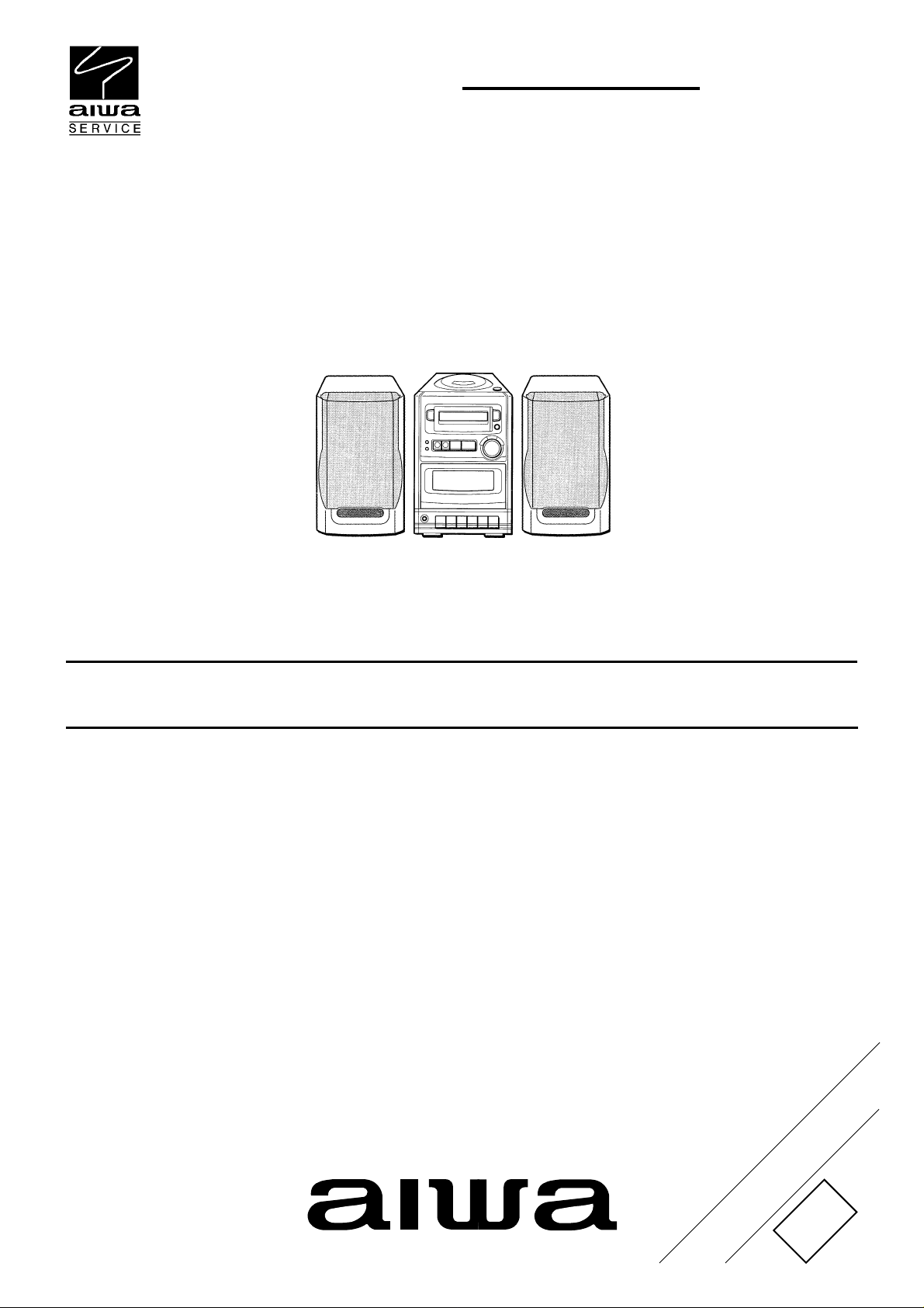
SERVICE MANUAL
COMPACT DISC
STEREO SYSTEM
This Service Manual is the “Revision Publishing” and replaces “Simple Manual”
LCX-K170(HRJST)(S/M Code No.09-993-324-7T1)
BASIC TAPE MECHANISM : TN21ZSC-1653
BASIC CD MECHANISM : KSM-2131 BDM
.
S/M Code No. 09-993-324-7R1
REVISION
DATA
Page 2

TABLE OF CONTENTS
SPECIFICATIONS .................................................................................................................................. 3
PROTECTION OF EYES FROM LASER BEAM DURING SERVICING/
Precaution to replace Optical block......................................................................................................... 4
ELECTRICAL MAIN PARTS LIST ....................................................................................................... 5-8
TRANSISTOR ILLUSTRATION .............................................................................................................. 8
WIRING-1 (MAIN) ............................................................................................................................. 9, 10
SCHEMATIC DIAGRAM-1 (MAIN).................................................................................................. 11, 12
WIRING-2 (VCD/FRONT) ................................................................................................................ 13-16
SCHEMATIC DIAGRAM-2 (VCD) ................................................................................................... 17, 18
SCHEMATIC DIAGRAM-3 (VCD) ................................................................................................... 19, 20
SCHEMATIC DIAGRAM-4 (FRONT) .............................................................................................. 21, 22
VOLTAGE CHART........................................................................................................................... 23-25
IC DESCRIPTION............................................................................................................................ 26-38
IC BLOCK DIAGRAM...................................................................................................................... 39, 40
ELECTRICAL ADJUSTMENT......................................................................................................... 41, 42
PRACTICAL SERVICE FIGURE........................................................................................................... 43
LCD DISPLAY....................................................................................................................................... 44
MECHANICAL EXPLODED VIEW 1/1............................................................................................ 45, 46
MECHANICAL PARTS LIST 1/1 ........................................................................................................... 47
TAPE MECHANISM EXPLODED VIEW 1/1 ......................................................................................... 48
TAPE MECHANISM PARTS LIST 1/1 .................................................................................................. 49
CD MECHANISM EXPLODED VIEW 1/1 ............................................................................................. 50
CD MECHANISM PARTS LIST 1/1 ...................................................................................................... 50
ACCESSORIES/PACKAGE LIST ......................................................................................................... 51
2
Page 3
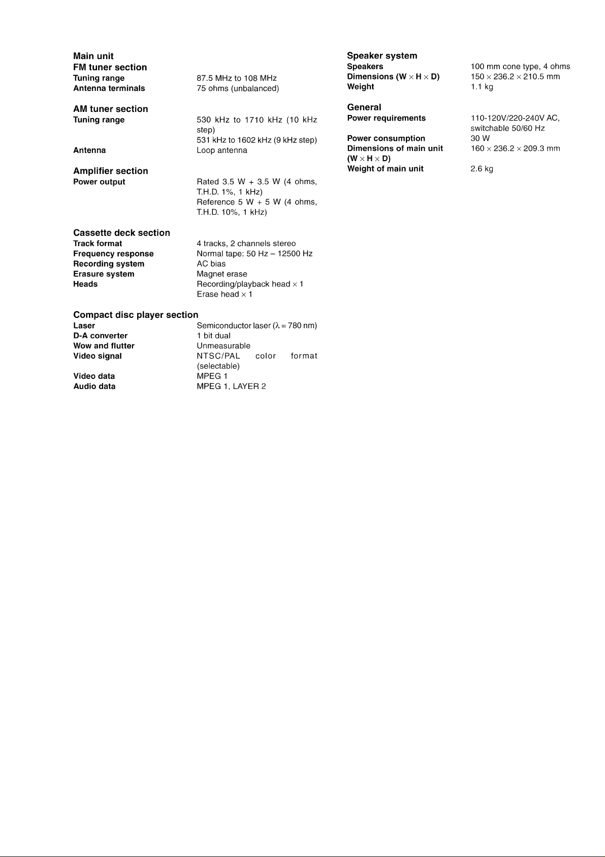
SPECIFICATIONS
Design and specifications are subject to change
•
without notice
.
3
Page 4
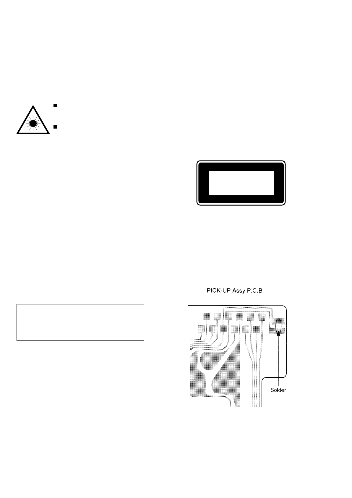
PROTECTION OF EYES FROM LASER BEAM DURING SERVICING
This set employs laser. Therefore, be sure to follow carefully the
instructions below when servicing.
WARNING!
WHEN SERVICING, DO NOT APPROACH THE LASER EXIT
WITH THE EYE TOO CLOSELY. IN CASE IT IS NECESSARY TO
CONFIRM LASER BEAM EMISSION. BE SURE TO OBSERVE
FROM A DISTANCE OF MORE THAN 30cm FROM THE
SURFACE OF THE OBJECTIVE LENS ON THE OPTICAL
PICK-UP BLOCK.
Caution: Invisible laser radiation when
open and interlocks defeated avoid exposure to beam.
Advarsel:Usynling laserståling ved åbning,
når sikkerhedsafbrydere er ude af funktion.
Undgå udsættelse for stråling.
VAROITUS!
Laiteen Käyttäminen muulla kuin tässä käyttöohjeessa mainitulla tavalla saattaa altistaa käyt-täjän turvallisuusluokan 1 ylittävälle näkymättömälle lasersäteilylle.
VARNING!
Om apparaten används på annat sätt än vad som specificeras i
denna bruksanvising, kan användaren utsättas för osynling
laserstrålning, som överskrider gränsen för laserklass 1.
CAUTION
Use of controls or adjustments or performance of procedures
other than those specified herein may result in hazardous
radiation exposure.
ATTENTION
L'utilisation de commandes, réglages ou procédures autres que
ceux spécifiés peut entraîner une dangereuse exposition aux
radiations.
ADVARSEL!
Usynlig laserståling ved åbning, når sikkerhedsafbrydereer ude
af funktion. Undgå udsættelse for stråling.
This Compact Disc player is classified as a CLASS 1 LASER
product.
The CLASS 1 LASER PRODUCT label is located on the rear
exterior.
CLASS 1
KLASSE 1
LUOKAN 1
KLASS 1
LASER PRODUCT
LASER PRODUKT
LASER LAITE
LASER APPARAT
Precaution to replace Optical block
(KSS-213B)
Body or clothes electrostatic potential could ruin
laser diode in the optical block. Be sure ground
body and workbench, and use care the clothes
do not touch the diode.
1) After the connection, remove solder shown in
the right figure.
4
Page 5

ELECTRICAL MAIN PARTS LIST
REF. NO PART NO. KANRI DESCRIPTION
IC
87-A20-591-010 IC,BA5417
87-A21-373-010 IC,BA328
87-A20-547-010 C-IC,CXA1992AR
87-A20-919-040 C-IC,BA5915FP
87-A20-917-010 C-IC,CXD2540Q-1/2
84-ZG1-698-010 C-IC,UPD78016FGC-553
87-A20-638-080 C-IC,PST9120
87-A20-918-040 C-IC,SM5878AN
87-A20-602-040 C-IC,M5291FP
87-A20-925-040 C-IC,BA05FP
87-A20-905-040 C-IC,BA033FP
87-A20-920-010 C-IC,CL680-D1
87-A20-921-040 C-IC,SN74LVU04APW
87-A20-962-040 C-IC,MSM54V16258B/BSL
84-ZG1-695-040 C-IC,LH5V2RN1
87-A20-975-040 C-IC,SN74LV74APW
87-A20-974-040 C-IC,LC74781M-9017
88-CG6-608-010 C-IC,LC867248A-XXX
87-A20-715-010 IC,M62439SP
87-A20-914-010 IC,SPS-442-1-F
87-070-127-110 IC,LC72131 D
87-A20-913-010 IC,LA1837NL
TRANSISTOR
87-026-231-080 CHIP-TRANSISTER,DTA124XK
89-111-625-080 TR,2SA1162 (0.15W)
87-026-290-080 TR,DTA124X
87-026-463-080 TR,2SA933S (0.3W)
87-026-237-080 CHIP-TR,DTC124XK
89-327-125-080 CHIP TR,2SC2712GR
87-026-228-080 C-TR,DTA124EK
87-026-580-080 C-TR,DTA123JK
87-026-470-080 TR,HN1C03F (0.3W)
87-A30-117-010 TR,2SA1357
87-CD7-603-080 TR,SS8050
87-026-291-080 TR,DTC124XS
87-A30-146-080 TR,2SD1468SR
89-113-184-080 TR,2SA1318T
87-026-462-080 TR,2SC1740 S(RS 0.3W)
87-A30-226-010 TR,2SB1655E
87-A30-227-080 TR,2SB1010Q
89-320-011-080 TR,2SC2001 (15W)
87-A30-196-080 TR,2SC4115SRS
89-327-143-080 TR,2SC2714 (0.1W)
87-026-230-080 CHIP-TR,DTA114YK
DIODE
87-020-465-080 DIODE,1SS133 (110MA)
87-070-136-080 ZENER,MTZJ5.1B
87-A40-246-080 DIODE,IN4148 T-72
87-020-027-080 CHIP-DIODE 1SS184
87-017-024-040 C-DIODE,DA204K
87-A40-180-040 C-DIODE,SB07-015C
87-A40-465-010 DIODE,FR202
87-070-345-080 DIODE,IN4148
87-070-022-010 DIODE,IN5402 (RECT)
87-A40-234-080 ZENER,MTZJ5.6A
87-070-334-080 ZENER,MTZJ10B
87-070-335-080 ZENER,MTZJ8.2B
87-017-931-080 ZENER,MTZJ5.6B
87-A40-347-080 ZENER,MTJ2.2B
MAIN C.B
!
87-033-213-080 CLAMP, FUSE
C1 87-010-404-080 CAP, ELECT 4.7-50V
NO.
REF. NO PART NO. KANRI DESCRIPTION
NO.
C2 87-010-405-080 CAP, ELECT 10-50V
C3 87-010-404-080 CAP, ELECT 4.7-50V
C4 87-010-405-080 CAP, ELECT 10-50V
C5 87-010-404-080 CAP, ELECT 4.7-50V
C6 87-010-405-080 CAP, ELECT 10-50V
C7 87-010-405-080 CAP, ELECT 10-50V
C8 87-010-404-080 CAP, ELECT 4.7-50V
C9 87-010-404-080 CAP, ELECT 4.7-50V
C10 87-018-131-080 CAP, CER 1000P-50V
C11 87-018-131-080 CAP, CER 1000P-50V
C301 87-018-128-080 CAP, CERA-SOL SS 560P
C302 87-010-378-080 CAP, ELECT 10-16V
C305 87-010-380-080 CAP, ELECT 47-16V
C307 87-010-405-080 CAP, ELECT 10-50V
C308 87-010-248-080 CAP, ELECT 220-10V
C309 87-010-405-080 CAP, ELECT 10-50V
C310 87-018-128-080 CAP, CERA-SOL SS 560P
C312 87-010-380-080 CAP, ELECT 47-16V
C313 87-010-378-080 CAP, ELECT 10-16V
C315 87-018-131-080 CAP, CER 1000P-50V
C318 87-018-131-080 CAP, CER 1000P-50V
C319 87-018-127-080 CAP, CER 470P-50V
C320 87-018-134-080 CAPACITOR,TC-U 0.01-16
C322 87-010-112-080 CAP, ELECT 100-16V
C325 87-010-401-080 CAP, ELECT 1-50V
C398 87-012-368-080 C-CAP,S 0.1-50 F
C401 87-010-401-080 CAP, ELECT 1-50V
C403 87-010-402-080 CAP, ELECT 2.2-50V
C404 87-010-401-080 CAP, ELECT 1-50V
C406 87-010-546-080 CAP, ELECT 0.33-50V
C407 87-010-546-080 CAP, ELECT 0.33-50V
C408 87-018-198-080 CAP,TC-U 2700P-16 X
C409 87-018-198-080 CAP,TC-U 2700P-16 X
C410 87-018-134-080 CAPACITOR,TC-U 0.01-16
C411 87-010-380-080 CAP, ELECT 47-16V
C412 87-010-380-080 CAP, ELECT 47-16V
C413 87-018-141-080 CAP, CERA-SOL SS 3.3P CH
C414 87-018-119-080 CAP, CER 100P-50V
C415 87-018-141-080 CAP, CERA-SOL SS 3.3P CH
C416 87-018-119-080 CAP, CER 100P-50V
C417 87-010-385-080 CAP, ELECT 220-25V
C418 87-018-134-080 CAPACITOR,TC-U 0.01-16
C419 87-010-380-080 CAP, ELECT 47-16V
C420 87-010-237-080 CAP, ELECT 1000-16V
C421 87-010-380-080 CAP, ELECT 47-16V
C422 87-010-237-080 CAP, ELECT 1000-16V
C425 87-016-658-090 CAP,E 4700-35 SMG
C426 87-010-197-080 CAP, CHIP 0.01 DM
C427 87-010-403-080 CAP, ELECT 3.3-50V
C428 87-018-205-080 CAP, CERA-SOL 0.022
C429 87-018-205-080 CAP, CERA-SOL 0.022
C430 87-018-205-080 CAP, CERA-SOL 0.022
C431 87-018-205-080 CAP, CERA-SOL 0.022
C432 87-018-134-080 CAPACITOR,TC-U 0.01-16
C433 87-018-134-080 CAPACITOR,TC-U 0.01-16
C434 87-018-134-080 CAPACITOR,TC-U 0.01-16
C435 87-010-248-080 CAP, ELECT 220-10V
C436 87-010-544-080 CAP, ELECT 0.1-50V
C437 87-010-380-080 CAP, ELECT 47-16V
C438 87-018-134-080 CAPACITOR,TC-U 0.01-16
C439 87-010-248-080 CAP, ELECT 220-10V
C440 87-010-404-080 CAP, ELECT 4.7-50V
C497 87-010-178-080 CHIP CAP 1000P
C498 87-010-178-080 CHIP CAP 1000P
C499 87-018-209-080 CAP, CER 0.1-50V
C501 87-010-401-080 CAP, ELECT 1-50V
C502 87-010-401-080 CAP, ELECT 1-50V
C504 87-010-545-080 CAP, ELECT 0.22-50V
C505 87-010-545-080 CAP, ELECT 0.22-50V
C506 87-018-119-080 CAP, CER 100P-50V
5
Page 6

REF. NO PART NO. KANRI DESCRIPTION
NO.
C508 87-010-545-080 CAP, ELECT 0.22-50V
C509 87-010-545-080 CAP, ELECT 0.22-50V
C510 87-010-263-080 CAP, ELECT 100-10V
C511 87-018-132-080 CAP, CER 2200P-16V
C512 87-010-263-080 CAP, ELECT 100-10V
C701 87-010-381-080 CAP, ELECT 330-16V
C702 87-010-404-080 CAP, ELECT 4.7-50V
C703 87-010-197-080 CAP, CHIP 0.01 DM
C704 87-010-197-080 CAP, CHIP 0.01 DM
C711 87-010-263-080 CAP, ELECT 100-10V
C712 87-010-196-080 CHIP CAPACITOR,0.1-25
C713 87-010-197-080 CAP, CHIP 0.01 DM
C714 87-010-197-080 CAP, CHIP 0.01 DM
C715 87-010-322-080 C-CAP,S 100P-50 CH
C721 87-010-312-080 C-CAP,S 15P-50 CH
C722 87-010-312-080 C-CAP,S 15P-50 CH
C723 87-010-178-080 CHIP CAP 1000P
C725 87-010-178-080 CHIP CAP 1000P
C727 87-010-196-080 CHIP CAPACITOR,0.1-25
C728 87-010-248-080 CAP, ELECT 220-10V
C756 87-010-197-080 CAP, CHIP 0.01 DM
C757 87-010-318-080 C-CAP,S 47P-50 CH
C758 87-010-149-080 C-CAP,S 5P-50 CH
C762 87-010-197-080 CAP, CHIP 0.01 DM
C763 87-010-194-080 CAP, CHIP 0.047
C764 87-010-319-080 C-CAP,S 56P-50 CH
C765 87-010-197-080 CAP, CHIP 0.01 DM
C766 87-010-197-080 CAP, CHIP 0.01 DM
C767 87-010-405-080 CAP, ELECT 10-50V
C768 87-010-197-080 CAP, CHIP 0.01 DM
C769 87-010-408-080 CAP, ELECT 47-50V
C770 87-010-194-080 CAP, CHIP 0.047
C771 87-010-407-080 CAP, ELECT 33-50V
C772 87-010-194-080 CAP, CHIP 0.047
C774 87-010-263-080 CAP, ELECT 100-10V
C775 87-010-404-080 CAP, ELECT 4.7-50V
C776 87-010-197-080 CAP, CHIP 0.01 DM
C777 87-010-400-080 CAP, ELECT 0.47-50V
C778 87-010-401-080 CAP, ELECT 1-50V
C779 87-010-401-080 CAP, ELECT 1-50V
C780 87-010-196-080 CHIP CAPACITOR,0.1-25
C781 87-010-405-080 CAP, ELECT 10-50V
C782 87-010-405-080 CAP, ELECT 10-50V
C783 87-010-197-080 CAP, CHIP 0.01 DM
C784 87-010-197-080 CAP, CHIP 0.01 DM
C785 87-010-403-080 CAP, ELECT 3.3-50V
C786 87-010-403-080 CAP, ELECT 3.3-50V
C789 87-010-179-080 CAP,CHIP S B1200P
C790 87-010-179-080 CAP,CHIP S B1200P
C791 87-010-405-080 CAP, ELECT 10-50V
C793 87-010-177-080 C-CAP,S 820P-50 SL
C794 87-010-406-080 CAP, ELECT 22-50
C795 87-010-194-080 CAP, CHIP 0.047
C796 87-010-403-080 CAP, ELECT 3.3-50V
C797 87-010-180-080 C-CER 1500P
C798 87-010-180-080 C-CER 1500P
C799 87-010-194-080 CAP, CHIP 0.047
C812 87-010-197-080 CAP, CHIP 0.01 DM
C814 87-010-197-080 CAP, CHIP 0.01 DM
C820 87-010-380-080 CAP, ELECT 47-16V
C821 87-010-197-080 CAP, CHIP 0.01 DM
C822 87-010-197-080 CAP, CHIP 0.01 DM
C823 87-010-197-080 CAP, CHIP 0.01 DM
C828 87-010-196-080 CHIP CAPACITOR,0.1-25
C829 87-010-196-080 CHIP CAPACITOR,0.1-25
C942 87-010-147-080 C-CAP,S 3P-50 CH
C959 87-010-196-080 CHIP CAPACITOR,0.1-25
C960 87-010-196-080 CHIP CAPACITOR,0.1-25
C961 87-010-152-080 C-CAP,S 8P-50 CH
CF801 87-018-209-080 CAP, CER 0.1-50V
REF. NO PART NO. KANRI DESCRIPTION
CF802 87-008-261-010 FILTER, SFE10.7MA5-A
CN401 87-099-043-010 CONN 2P EH
CN601 87-099-719-010 CONN,30P TYK-B(X)
CN701 87-033-239-010 TERMINAL,HSP-154V-2
!
F401 87-035-457-010 FUSE,3.15A 250V TW/C
FFE801 A8-8ZA-193-070 8ZA-1 YFEUNC
J401 88-CL5-609-010 TERMINAL,SP 4P
J403 88-CL5-608-010 JACK,3.6 S W/SW
J501 87-A60-354-010 JACK,PIN 2P MSP -242V-05
L401 87-005-192-080 COIL,4.7UH K EL0606
L770 87-005-847-080 COIL,2.2UH(CECS)
L771 87-A50-165-010 COIL,FM DET-N(TOK)
L773 87-A90-733-010 FLTR,PCFAZH-450 (TOK)
L832 87-005-847-080 COIL,2.2UH(CECS)
L982 87-NF4-650-010 COIL,AM PACK 4N(TOK)
R340 87-029-370-010 RES,FUSE 2.2-1/2W
R440 87-029-370-010 RES,FUSE 2.2-1/2W
SW301 88-CL6-608-010 SW,RP 8CL6
T301 88-CL6-609-010 COIL,BIAS 8CL6
X772 87-A70-061-010 VIB,XTAL 4.500MHZ CSA-309
VCD C.B
C101 87-010-182-080 C-CAP,S 2200P-50 B
C102 87-016-669-080 C-CAP,S 0.1-25 K B
C103 87-016-669-080 C-CAP,S 0.1-25 K B
C104 87-016-669-080 C-CAP,S 0.1-25 K B
C105 87-010-404-040 CAP,E 4.7-50 SME
C106 87-016-369-080 C-CAP,S 0.033-50 B K
C107 87-010-197-080 CAP, CHIP 0.01 DM
C108 87-010-401-040 CAP,E 1-50 SME
C109 87-010-382-040 CAP,E 22-25 SME
C110 87-010-213-080 C-CAP,S 0.015-50 B
C111 87-010-263-040 CAP,E 100-10
C112 87-010-197-080 CAP, CHIP 0.01 DM
C113 87-016-369-080 C-CAP,S 0.033-50 B K
C114 87-016-369-080 C-CAP,S 0.033-50 B K
C115 87-016-369-080 C-CAP,S 0.033-50 B K
C116 87-012-158-080 C-CAP,S 390P-50 CH
C117 87-012-154-080 C-CAP,S 150P-50 CH
C118 87-010-494-040 CAP,E 1-50 GAS
C119 87-010-313-080 CAP, CHIP 18P
C120 87-010-992-080 C-CAP,S 0.047-25 B
C121 87-010-992-080 C-CAP,S 0.047-25 B
C123 87-016-669-080 C-CAP,S 0.1-25 K B
C125 87-010-198-080 CAP, CHIP 0.022
C126 87-016-669-080 C-CAP,S 0.1-25 K B
C127 87-010-555-040 CAP,E 100-10 GAS
C130 87-010-555-040 CAP,E 100-10 GAS
C131 87-010-555-040 CAP,E 100-10 GAS
C132 87-010-178-080 CHIP CAP 1000P
C133 87-010-555-040 CAP,E 100-10 GAS
C136 87-010-196-080 CHIP CAPACITOR,0.1-25
C137 87-010-196-080 CHIP CAPACITOR,0.1-25
C138 87-010-184-080 CHIP CAPACITOR 3300P(K)
C139 87-010-197-080 CAP, CHIP 0.01 DM
C140 87-010-112-040 CAP,E 100-16
C141 87-010-196-080 CHIP CAPACITOR,0.1-25
C142 87-010-196-080 CHIP CAPACITOR,0.1-25
C143 87-010-213-080 C-CAP,S 0.015-50 B
C151 87-010-263-040 CAP,E 100-10
C152 87-010-197-080 CAP, CHIP 0.01 DM
C153 87-016-251-040 CAP,E 220-16 SMG
C154 87-010-190-080 S CHIP F 0.01
C155 87-010-184-080 CHIP CAPACITOR 3300P(K)
C156 87-010-992-080 C-CAP,S 0.047-25 B
C157 87-010-992-080 C-CAP,S 0.047-25 B
C158 87-012-156-080 C-CAP,S 220P-50 CH
C159 87-016-526-080 C-CAP,S 0.47-16 BK
C160 87-010-314-080 C-CAP,S 22P-50V
NO.
6
Page 7
E C B
C1
B2
E2
E1
B1
C2
E C B
E
B
C
2SA933
2SA1318
2SB1010
2SC2001
2SC4115
2SD1468
SS8050
2SC1740
DTA124XS
DTC124XS
RN1410
2SA1162
2SC2712
2SC2714
DTA114YK
DTA123JK
DTA124EK
DTA124XK
DTC124XK
B C E
E C B
2SB1655
2SA1357 HN1C03F
REF. NO PART NO. KANRI DESCRIPTION
C161 87-010-182-080 C-CAP,S 2200P-50 B
C162 87-010-178-080 CHIP CAP 1000P
C201 87-016-669-080 C-CAP,S 0.1-25 K B
C206 87-010-322-080 C-CAP,S 100P-50 CH
C207 87-010-322-080 C-CAP,S 100P-50 CH
C208 87-010-322-080 C-CAP,S 100P-50 CH
C209 87-010-322-080 C-CAP,S 100P-50 CH
C210 87-016-669-080 C-CAP,S 0.1-25 K B
C211 87-010-263-040 CAP,E 100-10
C212 87-010-197-080 CAP, CHIP 0.01 DM
C213 87-010-190-080 S CHIP F 0.01
C214 87-010-196-080 CHIP CAPACITOR,0.1-25
C234 87-010-196-080 CHIP CAPACITOR,0.1-25
C235 87-010-196-080 CHIP CAPACITOR,0.1-25
C238 87-010-184-080 CHIP CAPACITOR 3300P(K)
C252 87-010-197-080 CAP, CHIP 0.01 DM
C281 87-010-197-080 CAP, CHIP 0.01 DM
C282 87-010-197-080 CAP, CHIP 0.01 DM
C283 87-010-112-040 CAP,E 100-16
C284 87-010-196-080 CHIP CAPACITOR,0.1-25
C285 87-010-197-080 CAP, CHIP 0.01 DM
C286 87-010-197-080 CAP, CHIP 0.01 DM
C287 87-010-313-080 CAP, CHIP 18P
C288 87-010-313-080 CAP, CHIP 18P
C289 87-010-178-080 CHIP CAP 1000P
C290 87-010-178-080 CHIP CAP 1000P
C291 87-010-178-080 CHIP CAP 1000P
C292 87-010-178-080 CHIP CAP 1000P
C293 87-010-403-040 CAP,E 3.3-50 SME
C294 87-010-403-040 CAP,E 3.3-50 SME
C295 87-010-318-080 C-CAP,S 47P-50 CH
C296 87-010-318-080 C-CAP,S 47P-50 CH
C301 87-016-251-040 CAP,E 220-16 SMG
C302 87-012-140-080 CAP 470P
C302 87-010-178-080 CHIP CAP 1000P
C304 87-010-197-080 CAP, CHIP 0.01 DM
C304 87-010-384-040 CAP,E 100-25 SME
C305 87-010-982-040 CAP,E 33-25 GAS
C306 87-010-112-040 CAP,E 100-16
C307 87-010-179-080 CAP,CHIP S B1200P
C307 87-010-196-080 CHIP CAPACITOR,0.1-25
C308 87-010-263-040 CAP,E 100-10
C309 87-010-196-080 CHIP CAPACITOR,0.1-25
C310 87-010-263-040 CAP,E 100-10
C311 87-010-196-080 CHIP CAPACITOR,0.1-25
C312 87-010-178-080 CHIP CAP 1000P
C320 87-010-196-080 CHIP CAPACITOR,0.1-25
C331 87-010-197-080 CAP, CHIP 0.01 DM
C332 87-010-197-080 CAP, CHIP 0.01 DM
C333 87-010-197-080 CAP, CHIP 0.01 DM
C334 87-010-154-080 CAP CHIP 10P
C335 87-010-154-080 CAP CHIP 10P
C336 87-010-197-080 CAP, CHIP 0.01 DM
C338 87-010-263-040 CAP,E 100-10
C339 87-016-669-080 C-CAP,S 0.1-25 K B
C340 87-010-263-040 CAP,E 100-10
C341 87-010-196-080 CHIP CAPACITOR,0.1-25
C342 87-010-197-080 CAP, CHIP 0.01 DM
C343 87-010-197-080 CAP, CHIP 0.01 DM
C344 87-010-197-080 CAP, CHIP 0.01 DM
C348 87-010-322-080 C-CAP,S 100P-50 CH
C349 87-012-145-080 CAP, CHIP S 270P CH
C350 87-012-157-080 C-CAP,S 330P-50 CH
C351 87-012-154-080 C-CAP,S 150P-50 CH
C352 87-010-221-080 CAP,ELECT 470-10V
C353 87-010-197-080 CAP, CHIP 0.01 DM
C354 87-010-197-080 CAP, CHIP 0.01 DM
C355 87-010-197-080 CAP, CHIP 0.01 DM
C356 87-010-197-080 CAP, CHIP 0.01 DM
C357 87-010-197-080 CAP, CHIP 0.01 DM
NO.
REF. NO PART NO. KANRI DESCRIPTION
C358 87-010-197-080 CAP, CHIP 0.01 DM
C359 87-010-197-080 CAP, CHIP 0.01 DM
C360 87-010-197-080 CAP, CHIP 0.01 DM
C361 87-010-197-080 CAP, CHIP 0.01 DM
C362 87-010-374-080 CAP, ELECT 47-10V
C363 87-010-197-080 CAP, CHIP 0.01 DM
C364 87-010-555-040 CAP,E 100-10 GAS
C365 87-010-197-080 CAP, CHIP 0.01 DM
C366 87-010-374-080 CAP, ELECT 47-10V
C367 87-010-190-080 S CHIP F 0.01
C368 87-010-196-080 CHIP CAPACITOR,0.1-25
C369 87-010-196-080 CHIP CAPACITOR,0.1-25
C370 87-010-374-080 CAP, ELECT 47-10V
C371 87-010-197-080 CAP, CHIP 0.01 DM
C372 87-010-318-080 C-CAP,S 47P-50 CH
C374 87-010-197-080 CAP, CHIP 0.01 DM
C376 87-010-197-080 CAP, CHIP 0.01 DM
C379 87-010-494-040 CAP,E 1-50 GAS
C381 87-012-153-080 C-CAP,S 120P-50 CH
C382 87-016-526-080 C-CAP,S 0.47-16 BK
C386 87-010-197-080 CAP, CHIP 0.01 DM
C387 87-010-316-080 C-CAP,S 33P-50 CH
C388 87-A11-167-080 C-CAP,S 27P-50 F CH
C390 87-010-197-080 CAP, CHIP 0.01 DM
CN101 87-A60-424-010 CONN,16P V TOC-B
CN102 8Z-CL8-681-010 CONN ASSY,6P CD MOTOR
CN103 87-099-043-010 CONN 2P EH
J301 87-009-502-010 JACK,PIN 1P Y EARTH
L101 87-005-196-080 COIL,10UH
L301 87-A50-095-010 COIL,68UH RCR875D
L302 87-005-426-080 COIL,3.3UH K FLR50
L312 87-005-204-080 COIL,47UH
L313 87-005-189-080 COIL 2.7UH
L314 87-005-187-080 COIL,1.8UH
L315 87-005-204-080 COIL,47UH
L316 87-005-204-080 COIL,47UH
L317 87-005-204-080 COIL,47UH
L318 87-005-817-080 C-COIL, 33UH J FLC32
R130 87-022-364-080 C-RES,S 82K-1/10W F
R131 87-022-364-080 C-RES,S 82K-1/10W F
R132 87-022-364-080 C-RES,S 82K-1/10W F
R133 87-022-364-080 C-RES,S 82K-1/10W F
R134 87-022-364-080 C-RES,S 82K-1/10W F
R135 87-022-364-080 C-RES,S 82K-1/10W F
S201 88-CDV-607-010 SW,SL 2-2-3 SK23D02G9
X201 87-030-270-080 VIB,XTAL 16.9344MHZ
X202 87-A70-124-080 VIB,CER 8.0MHZ
X302 87-A70-125-080 VIB,XTAL 27MHZ 50PPM
FRONT C.B
C54 87-010-197-080 CAP, CHIP 0.01 DM
C55 87-010-401-080 CAP, ELECT 1-50V
C56 87-010-263-080 CAP, ELECT 100-10V
C501 87-010-248-080 CAP, ELECT 220-10V
C503 87-010-197-080 CAP, CHIP 0.01 DM
C508 87-010-197-080 CAP, CHIP 0.01 DM
C510 87-012-368-080 C-CAP,S 0.1-50 F
C511 87-010-400-080 CAP, ELECT 0.47-50V
C512 87-010-312-080 C-CAP,S 15P-50 CH
C513 87-010-320-080 CHIP CAP 68P
C514 87-010-316-080 C-CAP,S 33P-50 CH
C515 87-010-312-080 C-CAP,S 15P-50 CH
C516 87-010-314-080 C-CAP,S 22P-50 CH
C517 87-012-368-080 C-CAP,S 0.1-50 F
CN502 87-A60-390-010 CONN,3P H BGE TKX-P03P-A1
L500 87-003-226-080 MICRO INDUCTOR 100UH
LCD501 88-CL5-605-010 LCD,AIW4124-30PIN
S501 87-036-170-080 TACT SWITCH
S503 87-036-170-080 TACT SWITCH
NO.
REF. NO PART NO. KANRI DESCRIPTION
NO.
S504 87-036-170-080 TACT SWITCH
S505 87-036-170-080 TACT SWITCH
S506 87-036-170-080 TACT SWITCH
S507 87-036-170-080 TACT SWITCH
S508 87-036-170-080 TACT SWITCH
S509 87-036-170-080 TACT SWITCH
S511 87-036-170-080 TACT SWITCH
S512 87-036-170-080 TACT SWITCH
S513 87-036-170-080 TACT SWITCH
S514 87-036-170-080 TACT SWITCH
S515 87-036-170-080 TACT SWITCH
X501 87-030-273-010 VIB,XTAL 32.768K5PPM
X502 87-A70-070-080 VIB,CER 5.76MHZ CRHF
LED C.B
D545 87-CL5-602-010 LED,SLR342-MG3F
D546 87-CL5-602-010 LED,SLR342-MG3F
D547 87-CL5-602-010 LED,SLR342-MG3F
D548 87-CL5-602-010 LED,SLR342-MG3F
D549 87-CL5-602-010 LED,SLR342-MG3F
REF. NO PART NO. KANRI DESCRIPTION
D550 87-CL5-602-010 LED,SLR342-MG3F
D551 87-CL5-602-010 LED,SLR342-MG3F
D552 87-CL5-602-010 LED,SLR342-MG3F
D553 87-CL5-602-010 LED,SLR342-MG3F
AC C.B
SW C.B
!
87-033-213-080 CLAMP, FUSE
!
F2 87-035-219-010 FUSE,500MA 250V T218
!
SW451 87-A90-146-010 SW,SL 1-1-2
!
T1 87-A60-317-010 TERMINAL, 1P MSC
!
T2 87-A60-317-010 TERMINAL, 1P MSC
!
T3 87-A60-317-010 TERMINAL, 1P MSC
MOTOR C.B
M2 9X-262-513-210 SLED MOTOR ASSY
PIN3 91-564-722-110 CONNECTOR 6P
SW1 91-572-085-110 LEAF SW
NO.
• Regarding connectors, they are not stocked as they are not the initial order items.
The connectors are available after they are supplied from connector manufacturers upon the order is received.
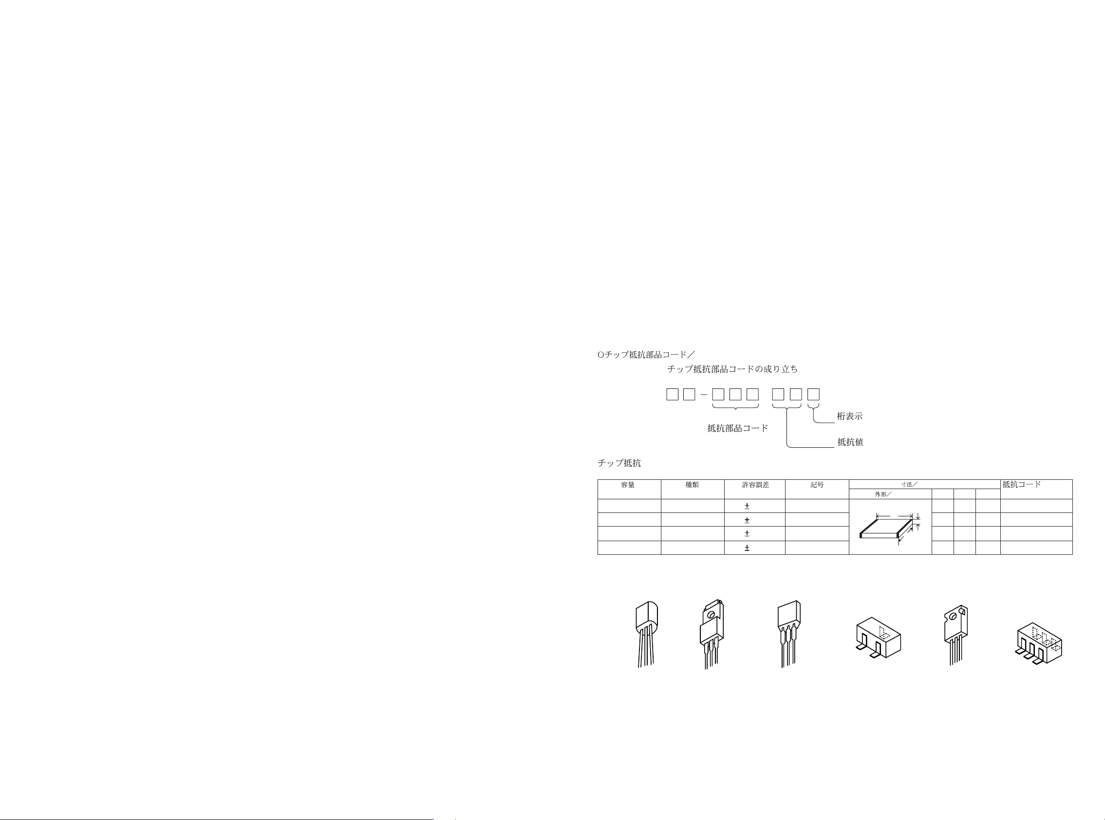
CHIP RESISTOR PART CODE
Chip Resistor Part Coding
88
A
Resistor Code
Chip resistor
Wattage Type Tolerance
1/16W 1005 5% CJ
1/16W
1/10W
1/8W
1608
2125
3216
5%
5%
5%
TRANSISTOR ILLUSTRATION
Symbol
Figure
Value of resistor
CJ
CJ
CJ
87
Form
L
W
Dimensions (mm)
LW t
1.0 0.5 0.35 104
t
1.6 0.8 0.45
2 1.25 0.45
1.6
0.55
3.2
Resistor Code
108
118
128
: A
: A
Page 8
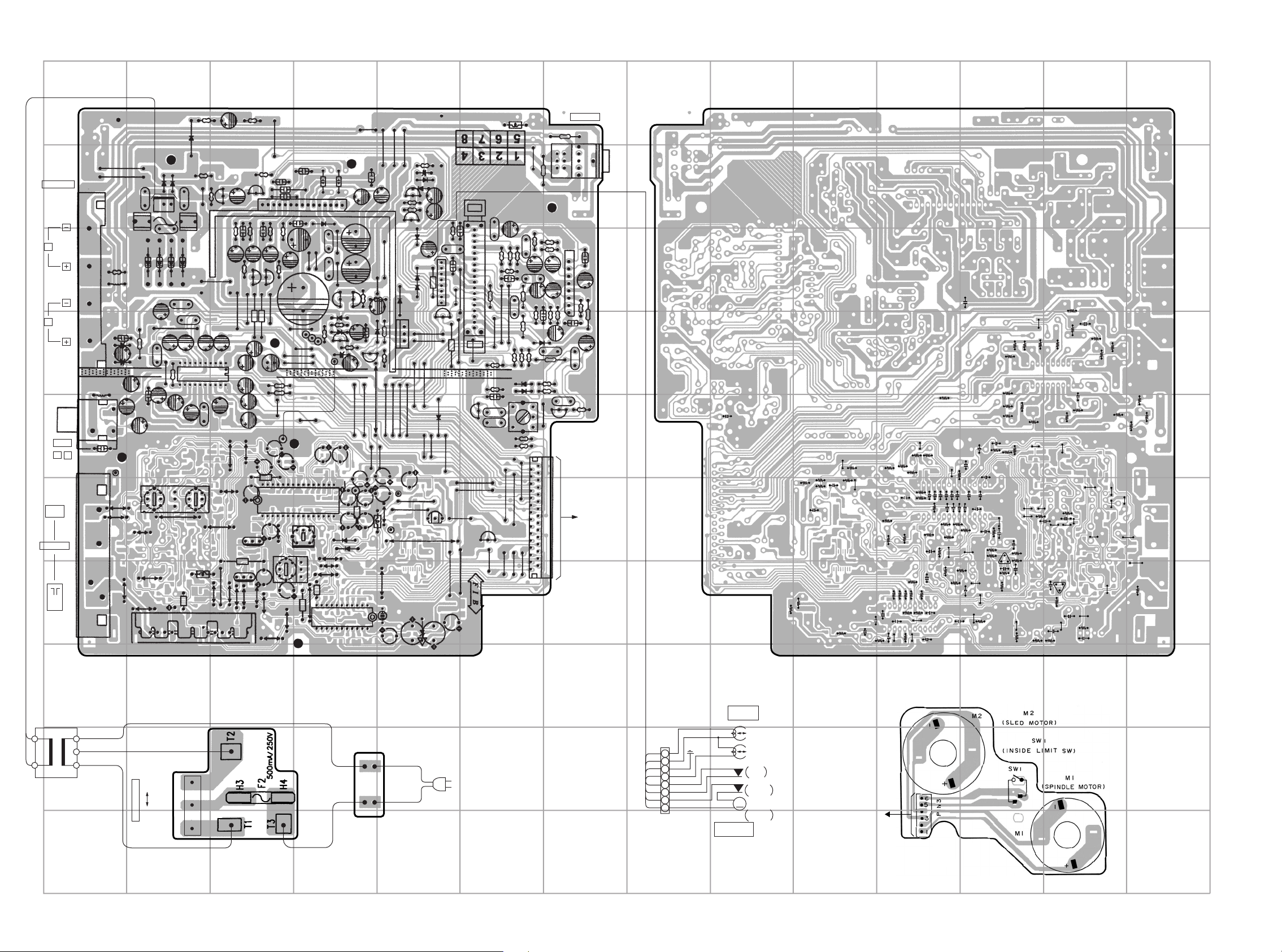
WIRING-1 (MAIN)
SPEAKER
R
L
AUX
L
AM
LOOP
ANTENNA
FM
75‰
7
J401
F401
R429
L402
C511
D501
C510
L501
J501
R
C499
CN701
H
654321
FH1
C404
R7
C512
D2
C501
C432
D420
D404
C429
C506
C502
C509
C402
C401
D401
CN401
C434
D406
C431
D403
C428
R521
C505
L982
MAIN C. B(INSERTED PARTS)
R4 R5
C1
D1
C416
C495
C418
VCC8V
F
R520
R519
L771
R718
[C]
C781
G
C417
D3022
H
11
12
C424
C423
R422
R420
D415
R719
C415
R421
D
C777
Q410
D412
D413
C774
16
15
D770
10
11
D402
FH2
D405
C430
C507
C508
C504
IC501
C950
R962
R415
C433
C405
C6
C503
L832
FFE801
Q404
R414
C411
12V
C2
C7
Q403
C427
15
C408 R405 R408
R409
C406 C407
R405
Q401
L_CH
1
C8
20
C771
C769
CF802
R830
C820
CF801
R402
R783
R413
C409
Q402
R403
C9
C5
C4
C795
30
1
SFR772
C496
C3
C403
C794
C414
R_CH
C425
C767
R410
C412
C791
L773
R407
TAPE-R
REC-R
D
IC741
C413
1
C419
R428
Q409
C437
Q408
C439
REC-L
C732
C785 C786
A
C779
R775
D771
IC720
L403
C410
C438
Q411
TAPE-L
1
22
C702
C420
C422
C440
D416
P-CONT
TU-L
C775
C421
R440
TU-R
L770
X772
Q406
R419
R418
R425
R424
C778
B
R423
D410
Q405
B
D302
C728
R417
D3021
D409
D301
Q407
C711
D721
C325
D414
8
R340
1
Q711
D411
C318
Q304
R61
D306
C701
C436
C435
R312
CN2
C963
C11
SW301
C10
C320
Q302
C304
R325
R318
R317
C319
C321
R325
R313
Q1
C302
D305
R328
R327
R324
C318
R323
C317
D304
R314
R329
R310
C306
C309
R315
R311
R309
CN601
R427
R303
C305
T301
C307
C312
R306
C315
C314
R322
PH1
D303
Q303
R428
R301
R302
R319
R320
J403
IC2
R307
C310
C313
C322
J403
PHONES
8
C301
C308
R305
1
C323
R321
C324
CON501
TO/FROM FRONT C.B
A
A
B
B
C
C
R308
D
D
E
E
F
F
G
G
1
MAIN C. B(CHIP PARTS)
C398
2
R714
R3
R713
C712
R711
R715
3
R798
C721
C703
C722
R707
R1
R773
R743
C727
C704
R781
R779
C756
R776 R774
R729
R726
R724
R728
R720
R708
R2
R712
C713
R705
456
C426
R404
C498
R518
R945
R821
C812
R523
C497
R525
R820
C829
R529
R401
R524
R15
R14
R540
R541
R822
R782
R780
R727
R722
C714
C776
C715
C798
R792
C723
R706
R797
R787
R761
R12
C797
R765
C790
C763
R772
C789
R791
C793
C766
R790
C725
C762
R771
C768
R793
C764
R788
C795
C780
C722
C799
C784
C756
R795
C757
R824
R806
C823
C738
R764
C770
R766
R832
R507
R594
R505
R763
C758
Q805
R827
R511
R508
R840
R509
R784
C822
C821
R506
R825
R823
R502
R510
R964
C955
R739
R503
C960
Q806
C814
C828
R830
7
PT 1
AC VOLTAGE
220 - 240V 110 - 120V
SW C. B
S451
H
H
AC
C. B
8
7
I
J
6
I
5
4
3
2
1
J
AZIMUTH
ADJ
M
M1
TAPE SPEED
ADJ
MA2
(L CH)
MA1
(R CH)
S1
PLAY
SW
S2
MOTOR
SW
M1
DECK
MOTOR
MOTOR C. B
TO / FROM
VCD C.B CN102
109
Page 9
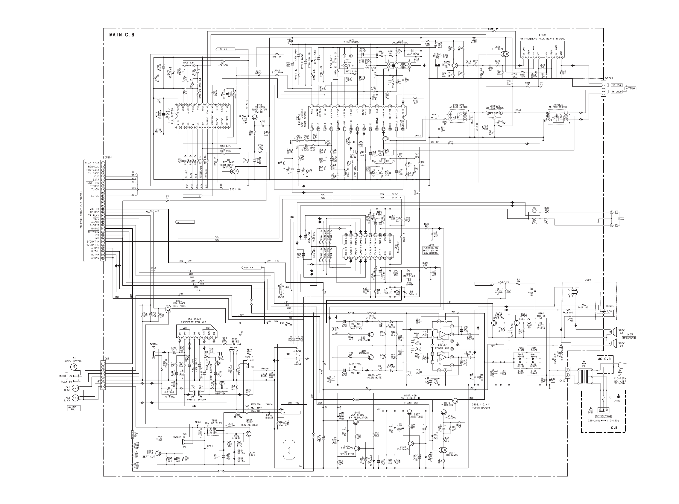
SCHEMATIC DIAGRAM-1 (MAIN)
S301
REC
PB
T218
SW
1211
Page 10
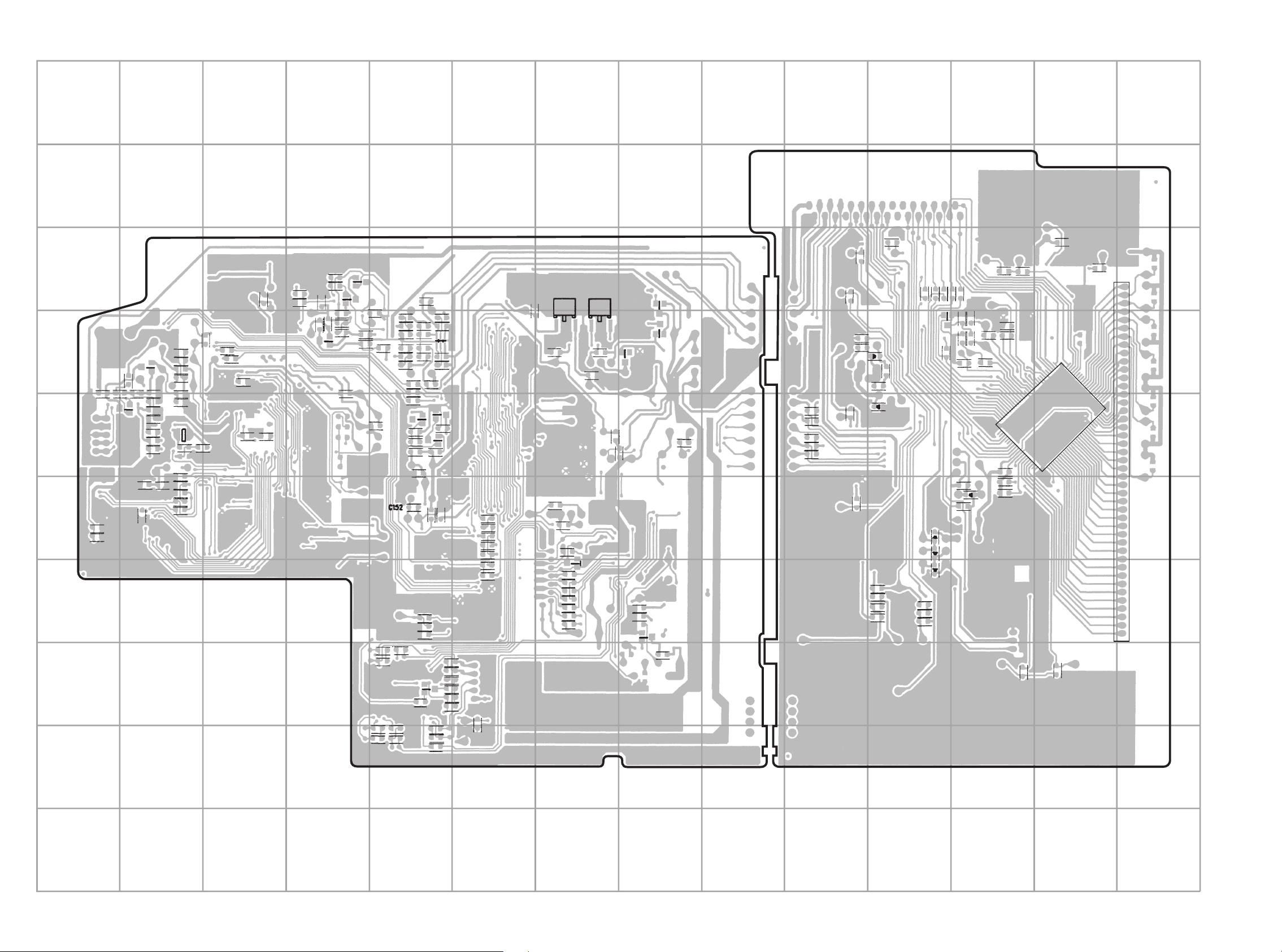
WIRING-2 (VCD/FRONT)
1
234567
8
9
10
11 12 13
14
A
FRONT C. B
(COMPONENT SIDE)
B
VCD C. B
C
D
R385
R394
R391
Q312
E
F
C369
C368
R386
R390
C386
C382
C367C371
R392
R367
G
H
I
Q311
C381
C384
R393
C387
R359
C349
C348
C350
C351
R360
R380
R396
R397
R384
R383
L318
(COMPONENT SIDE)
R379
C363
C365
R375
R374
C331
C388
T3
T4
T5
T1
C358C359
C372
JR211
JR212
R282
T2
C282
Q211
C284
C339
C287
C286
R284
C281
D211
R350
F–
F+
R139
T–T+
C137
Q212
C288
R287
R285
C285
R281
C289
R286
R288
R201
R202
R223
R226
C213
R200
C152
R138 R137
C136
R171
R140
TA1
D201
FE–0
R141
TA0
C291
C290
C292
Q103
R1
R2
R145
C134
R144
R169
R143
C138
C135
C210
R150
R156
C154
C159
Q201
C142
DSP
R146
R142
Q202
C214
R227
R291
C295
Q213
C296
R292
R168
C162
R170
R159
C160
R164
R165
SL+
SL–
UCON
C141
TST0
C309
TST1
IC303
2
TST3
TST2
R148
C132
C311
1
R136
D101
R135
R134
R133
R132
R131
R130
R129
IC302
2
R301
C307
R536
R535
C514C513
R548
100
R545R546
C54
R550
1
C510
R500
R554
R505
R508
R507
R506
R551
R515
D502
D501
D511
R532
R533
R534
Q502
R560
R570
D570
C508
C512
C516
R549C515
RGND
R542
R100
C112
VC
D301
Q303Q302
SL-0
JR104
C120
Q102
TE0
R107
SSP
R110
FE0
R523
R524
R518
R522
R525
C517
R557
R540
R530
R531
R538
R539
D509
R547
D500
R541
1
T6
IC501
81
R543
80
C503
30
R544
R537
43
31
50
51
1
LCD501
J
1413
Page 11
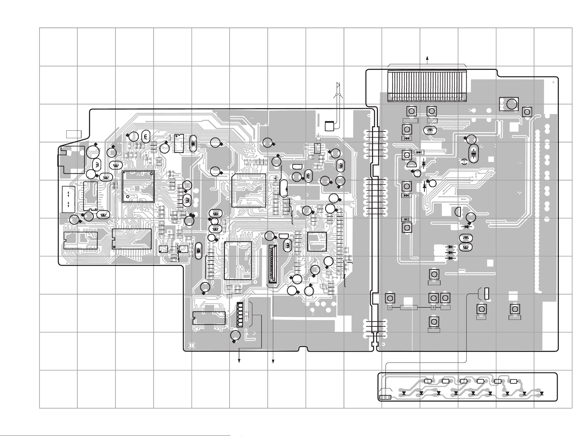
1
234567
8
9
10
11 12 13
14
A
TO/FROM MAIN C. B CN601
FRONT C. B
(CONDUCTOR SIDE)
B
S101
C306
JR102
C139
C111
R116
R117
R118
C114
R122
(OPEN / CLOSE)
C320
1
R302
IC301
4
C302
R303
C312
L301
C301
R113
R114
R112
C110
R109
26
27
39
C105
C127
CN103
8
5
C303
R304
14
13
1
5240
C130
R125
C109
C108
C104
R104
C102
C125
1
2
C304
C305
IC101
C121
JR103
R126
R111
C143
R108
C117
R149
R106
C107
C106
C116
R105
R103
JR101
C126
C123
L302
R101
C103
R102
C101
J16 J5 J6 J7 J9J10J1J4J15J2J3J8
J11J12 J13J14
S509
S503
REPEAT
S513
S511
Q501
S510
S512
VOLUME POP
S504
SET
L501
D509
C55
D500
C511
D502
D501
D511
S501
ROCK
S508
S504
JAZZ
Q570
D570
S503
C56
X501
CON501
IC502
X502
C501
L500L502
1
3
CN501
S514
AUX BAND
S507
S515
VCD C. B
(CONDUCTOR SIDE)
C
J301
VIDEO
OUT
C364
C352
S201
NTSC
AUTO
PAL
44
IC314
1
J301
C370
13
IC317
24
C379
C366
L316
L314
1
C360
32
IC315
1
L313
C361
32
33
12
1
L317
23
22
D
E
F
G
C362
R378
R373
R351
R377
R352
R372
IC311
L315
C332
R376
C357
C390
C356
C376
17
16
R294
R296
97128
64
C333
96
65
C374
R387
IC316
C283
R295
R293
R398
R363
R362
R361
R353
R382
C353
C341
1
R283
12
C342
R365
R366
R364
R381
C355
R357
C336
R388R267
C334
C343
C344
24
X201
C293
13
IC211
C294
C338
L312
R358
C354
R266
R368
IC313
C335
R371
114
C340
R370
R152
R151
R153
C157
R154
R155
C155
C153
C211
X302
L201
L151
C151
1
C156
24
R160
80
25
R158
C161
1
IC201
16
17
R221
R222
64
C158
1
R157
R207
65
40
R147
64
41
C308
R215
49
48
33
32
IC151
R205
R204
R210
R205
C131
1
16
C310
IC203
R213
R211
R203
R224
C201
Q101
L101
CN101
R121
R123
R124
C119
C133
C118
Q301
X202
C206
R214
R212
C207
C208
C209
C113
C115
H
IC102
CN102
6
1528
C140
I
TO/FROM
CD MOTOR C.B
J
TO/FROM
PICK UP ASSY
LED C. B
CN502
D553
R561 R564 R562 R565 R563 R567
D552
D551
D550
D549
D548
D547
D546
D545
1615
Page 12
SCHEMATIC DIAGRAM-2 (VCD 1/2)
SW
SWITCHING REGULATOR
AC/DC CONVERTER
1817
Page 13

SCHEMATIC DIAGRAM-3 (VCD 2/2)
VCK OSC
DELAY
SW
OR GATE
NOISE SHAPER
D/A CONVERTER
MUTE
1/2 DIVIDE
2019
Page 14

SCHEMATIC DIAGRAM-4 (FRONT)
D545-549
SLR,342-MG3F
TO/FROM VCD C.B
2221
Page 15

VOLTAGE CHART
23
Page 16

242526
Page 17

Page 18

IC DESCRIPTION
IC, CXA1992AR
Pin No. Pin Name I/O Description
1
2
3
FEO
FEI
FDFCT
Output terminal for focus error amplifier. Internally connected to window comparator
O
input for bias condition.
Input terminal for focus error.
I
Capacitor connection terminal for time constant used when there is defect.
I
10
11
12
13
14
15
16
4
5
6
7
8
9
FGD
FLB
FE_O
FEM
SRCH
TGU
TG2
FSET
TA_M
TA_O
SL_P
SL_M
SL_O
This pin is connected to GND via capacitor when high frequency gain of the focus
I
servo is attenuated.
This is a pin where the time constant is externally connected to raise the low frequency
I
gain of the focus servo.
Focus drive output.
O
Focus amplifier inverted input pin.
I
This is a pin where the time constant is externally connected to generate the focus
I
search waveform.
This is a pin where the selection time constant is externally connected to set the
I
tracking servo the high frequency gain.
This is a pin where the selection time constant is externally connected to set the
I
tracking high frequency gain.
Pin for setting peak of the phase compensator of the focus tracking.
I
Tracking amplifier inverted input pin.
I
Tracking drive output.
O
Sled amplifier non-inverted input pin.
I
Sled amplifier inverted input pin.
I
Sled drive output.
O
17
18
19
20
21
22
23
24
25
26
27
28
29
30
31
ISET
Vcc
LOCK
CLK
XLT
DATA
XRST
C_OUT
SENS1
SENS2
FOK
CC2
CC1
CB
CP
The current which determines height of the focus search, track jump and sled kick is
I
input with external resistance connected.
Power supply.
I
“L” setting starts sled disorder-prevention circuit. (Not pull-up resistance)
I
Clock input for serial data transfer from CPU. (No pull-up resistance)
I
Latch input from CPU. (No pull-up resistance)
I
Serial data input from CPU. (No pull-up resistance)
I
Reset system at “L” setting. (No pull-up resistance)
I
Signal output for track number counting.
O
FZC, DFCT1, TZC, BALH, TGH, FOH, or ATSC is output depending on the
O
command from CPU.
DFCT2, MIRR, BALL, TGL or FOL is output depending on the command from CPU.
O
Output terminal for focus OK comparator.
O
Input pin where the DEFECT bottom hold output is capacitance coupled.
I
DEFECT bottom-hold output terminal. Internally connected to interruption comparator
O
input.
Connection terminal for DEFECT bottom-hold capacitor.
I
Connection terminal for MIRR hold-capacitor.
I
Anti-reverse input terminal for MIRR comparator.
Page 19

Pin No. Pin Name I/O Description
32
33
34
RF_I
RF_O
RF_M
I
Input terminal by capacity combination of RF summing amplifier.
O
Output terminal of RF summing amplifier. Checkpoint of Eye pattern.
Anti-reverse input terminal for RF summing amplifier.
The gain of RF amplifier is decided by the connection resistance between RF_M and
I
RFO terminals.
35
36
37
38, 39
40
41, 42
43
44
45
46
47
48
49
50
RFTC
LD
PD
PD1, PD2
FEBIAS
F, E
EI
VEE
TEO
LPFI
TEI
ATSC
TZC
TDFCT
O
I/O
—
—
O
This is a pin where the selection time constant is externally connected to control the
I
RF level.
APC amplifier output terminal.
I
APC amplifier input terminal.
RFI-V amplifier inverted input pin.
I
These pins are connected to the A+C and B+C pins of the optical pickup, receiving by
currents input.
Bias adjustment pin of the focus error amplifier.
F and EIV amplifier inverted input pins.
I
These pins are connected to the F and E of the optical pickup, receiving by current
input.
Gain adjustment pin of the I-V amplifier E. (When not in use of BAL automatic
adjustment)
GND connection pin.
Output terminal for tacking-error amplifier. Output E-F signal.
I
BAL adjustment comparator input pin. (Input through LPF from TEO)
I
Input terminal for tracking error.
I
Window-comparator input terminal for detecting ATSC.
I
Input terminal for tracking-zero cross comparator.
I
Capacitor connection pin for the time constant used when there is defect.
51
52
VC
FZC
O
Output terminal for DC voltage reduced to half of VCC+VEE.
I
Input terminal for focus-zero cross comparator.
27
Page 20

IC, CXD2540Q
Pin No. Pin Name I/O Description
1
2
3
FOK
FSW
MON
I
Focus OK input. Used for SENS output and the servo auto sequencer.
O
Spindle motor output filter switching output.
O
Spindle motor on/off control output.
10
11
12
13
14
15
16
17
18
19
20
21
22
4
5
6
7
8
9
MDP
MDS
LOCK
NC
VCOO
VCOI
TEST
PDO
VSS
PWMI
V16M
VCTL
VPCO
VCKI
FILO
FILI
PCO
AVSS
CLTV
O
Spindle motor servo control.
O
High, when sampled value of GFS at 460Hz is high.
O
Low, when sampled value of GFS at 460Hz is low by 8 times successively.
O
Analog EFM PLL oscillation circuit output.
I
Analog EFM PLL oscillation circuit input. fLOCK=8.6436MHz.
I
TEST pin.
O
Analog EFM PLL charge pump output.
GND.
I
Spindle motor external control input.
O
VCO2 oscillation output for the wide-band EFM PLL.
I
VCO2 control voltage input for the wide-band EFM PLL.
O
Wide-band EFM PLL charge pump output.
I
VCO2 oscillation input for the wide-band EFM PLL.
O
Multiplier PLL (slave=digital PLL) filter output.
I
Multiplier PLL filter input.
O
Multiplier PLL charge pump output.
Analog GND.
I
Multiplier VCO1 control voltage input.
23
24
25
26
27
28
29
30
31
32
33
34
35
36
37
38
AVDD
RF
BIAS
ASYI
ASYO
ASYE
NC
PSSL
WDCK
LRCK
VDD
DA16
DA15
DA14
DA13
DA12
Analog power supply (5V).
I
EFM signal input.
I
Constant current input of the asymmetry circuit.
I
Asymmetry comparator voltage input.
O
EFM full-swing output.
I
Low: asymmetry circuit off; high: asymmetry circuit on.
I
Audio data output mode switching input. Low: serial output; high: parallel output.
O
D/A interface for 48-bit slot. Word clock f=2Fs.
O
D/A interface for 48-bit slot. LR clock f=Fs.
Power supply (5V).
DA16 (MSB) output when PSSL=1.
O
48-bit slot serial data (two’s complement, MSB first) when PSSL=0.
O
DA15 output when PSSL=1. 48-bit slot bit clock when PSSL=0.
DA14 output when PSSL=1.
O
64-bit slot serial data (two’s complement, LSB first) when PSSL=0.
O
DA13 output when PSSL=1. 64-bit slot bit clock when PSSL=0.
O
DA12 output when PSSL=1. 64-bit slot LR clock when PSSL=0.
28
Page 21

Pin No. Pin Name I/O Description
39
40
41
DA11
DA10
DA09
O
DA11 output when PSSL=1. GTOP output when PSSL=0.
O
DA10 output when PSSL=1. XUGF output when PSSL=0.
O
DA09 output when PSSL=1. XPLCK output when PSSL=0.
42
43
44
45
46
47
48
49
50
51
52
53
54
55
56
57
58
59
60
DA08
DA07
DA06
DA05
DA04
DA03
DA02
DA01
APTR
APTL
VSS
XTAI
XTAO
XTSL
FSTT
FSOF
C16M
MD2
DOUT
O
DA08 output when PSSL=1. GFS output when PSSL=0.
O
DA07 output when PSSL=1. RFCK output when PSSL=0.
O
DA06 output when PSSL=1. C2PO output when PSSL=0.
O
DA05 output when PSSL=1. XRAOF output when PSSL=0.
O
DA04 output when PSSL=1. MNT3 output when PSSL=0.
O
DA03 output when PSSL=1. MNT2 output when PSSL=0.
O
DA02 output when PSSL=1. MNT1 output when PSSL=0.
O
DA01 output when PSSL=1. MNT0 output when PSSL=0.
Aperture compensation control output.
O
This pin outputs a high signal when the right channel is used.
Aperture compensation control output.
O
This pin outputs a high signal when the left channel is used.
GND.
I
Crystal oscillation circuit input.
O
Crystal oscillation circuit output.
I
Crystal selector input.
O
2/3 frequency divider output for Pins 53 and 54.
O
1/4 frequency divider output for Pins 53 and 54.
O
16.9344MHz output. (V16M output in CLV-W and CAV-W modes)
I
Digital-out on/off control. High: on; low: off
O
Digital-out output.
61
62
63
64
65
66
67
68
69
70
71
72
73
74
75
76
EMPH
WFCK
SCOR
SBSO
EXCK
SQSO
SQCK
MUTE
SENS
XRST
DATA
XLAT
VDD
CLOK
SEIN
CNIN
—
Outputs a high signal when the playback disc has emphasis, and a low signal when
O
there is no emphasis.
I
WFCK (write frame clock) output.
O
Outputs a high signal when either subcode sync S0 or S1 is detected.
O
Sub P to W serial output.
I
SBSO readout clock input.
O
Sub Q 80-bit and PCM peak, level metter and internal status outputs.
I
SQSO readout clock input.
I
High: mute; low: release
SENS output to CPU.
I
System reset. Reset when low.
O
Serial data input from CPU.
O
Latch input from CPU. Serial data is latched at the falling edge.
Power supply (5V).
O
Serial data transfer clock input from CPU.
I
SENS input from SSP.
I
Track jump count signal input.
29
Page 22

Pin No. Pin Name I/O Description
77
78
79
DATO
XLTO
CLKO
Serial data output to SSP.
O
Serial data latch output to SSP. Latched at the falling edge.
O
Serial data transfer clock output to SSP.
O
80
Notes)
• The 64-bit slot is an LSB first, two’s complement output, and the 48-bit slot is an MSB first, two’s complement output.
• GTOP is used to monitor the frame sync protection status. (High: sync protection window open.)
• XUGF is the negative pulse for the frame sync obtained from the EFM signal. It is the signal before sync protection.
• XPLCK is the inverse of the EFM PLL clock. The PLL is designed so that the falling edge and the EFM signal transition point
coincide.
• GFS goes high when the frame sync and the insertion protection timing match.
• RFCK is derived from the crystal accuracy, and has a cycle of 136µ.
• C2PO represents the data error status.
• XRAOF is generated when the 32K RAM exceeds the ±28F jitter margin.
MIRR
Mirror signal input. Used when the number of tracks is 128 or more for the 2N-track
I
jump and M track move of the auto sequencer.
30
Page 23

IC, CL680-D1
Pin No. Pin Name I/O Description
1
NC
—
No connection.
2
3
4
5
6
7-9
10-15
16
17
18
19
20
21
22
23-29
30-36
37
38
VSS
CD BCK
CD DATA
CD LRCK
CD C2PO
NC
MD0-MD5
VSS
MD6
VDD3
MD7
VSS
MD8
VDD3
MD9-MD15
NC
________
MCE
__________
MWE
—
—
I/O
—
I/O
—
I/O
—
I/O
—
I/O
—
—
O
GND.
I
Bit clock input from CD DSP.
I
Data input from CD DSP.
I
LRCK input from CD DSP.
I
C2 pointer input from CD DSP.
No connection.
DRAM/ROM interface. (DATA)
Ground.
DRAM/ROM interface. (DATA)
Power supply 3.3V.
DRAM/ROM interface. (DATA)
Ground.
DRAM/ROM interface. (DATA)
Power supply 3.3V.
DRAM/ROM interface. (DATA)
No connection.
ROM chip enable.
DRAM write enable.
39
40
41
42
43
44-46
47
48
49
50-52
53
54
55
56-58
59
60
61
VSS
________
CAS
VDD3
___________
RASO
___________
RASI
MA10-MA8
VSS
MA7
VDD3
MA6-MA4
VSS
MA3
VDD3
MA2-MA0
PGIO7
______________
RESET
VDD MAX IN
—
O
—
O
O
O
—
O
—
O
—
O
—
O
I/O
—
Ground.
DRAM/ROM interface.
Power supply 3.3V.
DRAM/ROM interface.
DRAM/ROM interface. (Address)
Ground.
DRAM/ROM interface. (Address)
Power supply 3.3V.
DRAM/ROM interface. (Address)
Ground.
DRAM/ROM interface. (Address)
Power supply 3.3V.
DRAM/ROM interface. (Address)
Programmable I/O.
I
Reset input.
Power supply - VDDMAX. (5.0V)
62-64
65
66
67
68
NC
AGND DAC
A DAC
COMP OUT
AGND DAC
—
—
—
—
No connection.
Analog ground.
Analog power supply (DAC) : 3.3V.
O
Composite out.
Analog ground.
31
Page 24

Pin No. Pin Name I/O Description
Video signal “Y” OUT.
69
Y OUT
O
70
71
72
73
74
75
76
77-79
80
81
82
83, 84
85
86
87
88
89, 90
AVDD DAC
AGND DAC
R REF
V REF
AVDD DAC
C OUT
AGND DAC
CLK SEL0-2
VSS
CLK SEL3
VDD3
CLK SEL4, 5
AGND PLL
DA XCK
AVDD PLL
DA EMP
PGIO5, O6
—
—
—
O
—
—
—
—
—
O
I/O
Analog power supply (DAC) 3.3V.
Analog ground.
Reference resistor input.
I
Voltage reference input.
I
Analog power supply (DAC) : 3.3V.
Video signal “C” out.
Analog ground.
Clock selection input.
I
Ground.
Clock selection input.
I
Power supply 3.3V.
Clock selection input.
I
Analog ground.
DA XCK (16.933MHz) input.
I
Analog power supply 3.3V.
DAC-emphasis output.
91
92
93
94
95
96
97
98
99
100
101
102
103
104
105
106
107
PGIO0
PGIO8
______________ ______________
VSYNC/CSYNC
AVDD PLL
VID_DAC_CK
PROC_CK
AUD_XCK
AGND PLL
VSS
NC
______________
HSYNC
VDD3
VCK OUT
VSS
GCK
VCK
GCK OUT
I/O
I/O
O
—
O
O
O
—
—
—
O
—
O
—
O
Programmable I/O.
______________ ______________
VSYNC/CSYNC output.
Analog power supply (PLL) 3.3V.
Video DAC clock.
Processor clock.
Audio XCK.
Analog ground.
Ground.
No connection.
______________
HSYNC output.
Power supply 3.3V.
VCK out.
Ground.
Global clock signal input. (42.3MHz)
I
Video clock signal input. (27.0MHz)
I
Global clock signal output. (27.0MHz)
108
109
110
111
112
113
DA LRCK
VDD MAX OUT
DA DATA
DA BCK
HD OUT
HRDY
O
—
O
O
O
O
DAC-LRCK output.
Power supply (VDD MAX) : 5.0V.
DAC-PCM data output.
DAC-BIT clock output.
Micon interface. (Data out)
Micon interface. (Host ready)
32
Page 25

Pin No. Pin Name I/O Description
__________
114
HINT
Micon interface. (Host interrupt)
O
115
116
117
118
119
120
121
122
123
124
125
126-128
CDG SCK
VSS
HCK
VDD3
HD IN
VDD3
HSEL
CDG DATA
CDG VFSY
CDG SOSI
DSP-XCK
NC
—
—
—
—
CD-G serial clock input.
I
Ground.
Micon interface. (Host clock)
I
Power supply 3.3V.
Micon interface. (Host data in)
I
Power supply 3.3V.
Micon interface. (Host select in)
I
CD-G data input.
I
CD-G VFSY input.
I
CD-G SOSI input.
I
DSP-XCK output.
O
No connection.
33
Page 26

IC, LC867248A-5H31
Pin No. Pin Name I/O Description
1
2
3
O-SCONTM
O-SCONTL
O-TUDI
O
M62439SP control. open drain output.
O
O
Tuner control. CMOS output.
4
5
6
7
8
9
10
11
12
13, 14
15
16, 17
18
19
20
21
22
23
24
I-TUDO
O-TUCL
O-COIN
I-SQOUT
___________
O-CQCK
O-RWC
_______________
O-CLKSFT
I-TMBASE
____________
I-RESET
NC
VSS1
CF1, CF2
VDD1
I-KEY0
I-KEY1
I-RDSIG
I-WRQ
I-DRF
I-DOOR
O
O
O
O
O
I/O
—
I/O
—
I
Tuner control.
Tuner control. CMOS output.
CD control. open drain output.
I
CD control.
CD control. open drain output.
Clock shift output. “L” during shift. open drain output.
I
8 Hz time base input.
I
Reset input.
Not used.
GND.
Main clock input/output 5.76 MHz.
+5V.
I
KEY0 A/D input.
I
KEY1 A/D input.
I
RDS signal level input. (A/D input)
I
CD control.
I
I
CD door SW detection SW input. “L” at CLOSE.
25
26
27
28
29
30
31
32
33
34
35
36-38
39-55
56
57
58-79
80
81
82
I-PUIN
I-SWTAPE
________________
I-STEREO
I-RDCL
________
I-REM
___________
I-HOLD
I-RDDT
I-TPREC
I-TPPLAY
O-PL
O-MOTOR
NC
S9-S25
VDD2
VSS2
S26-S47
I-CLKDSP
I-AS
__________
I-STOP
O
O
O
O
—
—
O
I
CD pick-up detection SW input. “L” at ON.
I
Tape detection SW input. (A/D input)
I
Monaural/stereo indication selector input. “L” at stereo.
I
RDS clock input.
I
Remote control input. (fall-down edge interrupt input)
I
Hold mode detection. “L” at hold mode.
I
RDS data input.
I
Tape REC detection input. “H” at REC.
I
Tape PLAY detection input. “H” at PLAY.
Mechanism deck plunger solenoid ON/OFF output. “H” at ON. CMOS output .
Mechanism deck motor ON/OFF output. “H” at ON. CMOS output.
Not used.
LCD SEG terminal Initial setting output. (S10 to S16)
+5V.
GND.
LCD SEG terminal .
I
Watch indication select input “L”: 12H. “H”: 24H.
I
Auto stop. counter input .
Tape stop input.
I
34
Page 27

Pin No. Pin Name I/O Description
83-86
87
COM0-COM3
I-INIT
O
LCD common output.
I
Initial setting input.
88
89
90
91
92
93
94
95
96
97
98
99
100
O-BEAT
VSS3
VDD3
O-QSDON
O-TUCE
O-CD-ON
O-TU-ON
O-RMT
________
O-REC/PB
O-MUTE
O-PCONT
O-BIAS
NC
—
—
O
Beat selector output. “H” during selection. CMOS output .
GND.
5V.
O
Q sound ON/OFF output. “H” at ON. CMOS output .
O
Tuner chip enable output. CMOS output .
O
“H” output during CD function. CMOS output.
O
“H” output during TU function. Open drain output.
O
REC mute output. “H” during mute. Open drain output.
O
REC/PB select output. “H” during PB. Open drain output.
O
Mute output. “H” during mute. Open drain output.
O
Power control output. “H” at ON. CMOS output.
O
REC bias ON/OFF output. “H” at ON. Open drain output.
O
Not used.
35
Page 28

IC, SM5878AN
Pin No. Pin Name I/O Description
1
2
3
MUTE
DEEM
CKO
MODE = H: Soft mute ON/OFF terminal. (Mute at H).
I
MODE = L: Attenuator level DOWN/UP terminal. (DOWN at H).
I
De-emphasis ON/OFF terminal. (De-emphasis ON at H).
O
Oscillator clock output. (16.9344 MHz).
10
11
12
13
14
15
16
17
18
19
20
21
22
4
5
6
7
8
9
DVSS
BCKI
DI
DVDD
LRCI
TSTN
TO1
AVDDL
LO
AVSS
RO
AVDDR
MUTEO
XVDD
XTI
XTO
XVSS
DS
RSTN
—
—
O
—
O
—
O
—
O
—
O
—
Digital VSS terminal.
I
Bit clock input terminal.
I
Serial data input terminal.
Digital VDD terminal.
I
Sample rate clock (fs) input terminal. (H = L ch/L = R ch).
I
Test input. (“H” or open during normal operation)
Test output 1. (Normally low level output).
Analog VDD terminal. (For L ch).
Left channel analog output terminal.
Analog VSS terminal.
Right channel analog output terminal.
Analog VDD terminal. (For R ch).
Infinity zero detection output.
X’tal system VDD terminal.
I
X’tal oscillator terminal. (Or external clock input terminal of 16.9344 MHz).
X’tal oscillator terminal.
X’tal system VSS terminal.
I
Double-speed/normal playback selection. (Double-speed at H).
I
Reset terminal. (Reset at L).
23
24
MODE
ATCK
I
Soft mute/Attenuator mode selection. (Soft mute at H).
I
Attenuator level setup clock (Ignored when MODE = H).
36
Page 29

IC, LC74781M-9017
Pin No. Pin Name I/O Description
1
2
3
VSS1
Xtal IN
Xtal OUT
—
GND connection terminal. (Digital ground terminal).
I
External X’tal and capacitor for internal sync generator, or the external clock are
connected to this terminal. (2fsc or 4fsc).
O
10
11
12
4
CTRL1
Either the external clock input mode or the X’tal generator mode is selected by this
I
selector terminal. L: X’tal generator mode, H: External clock input.
Blank signal (character and the green ORed signal) is output from this terminal.
5
BLANK
(MODE 0: composite sync signal is output at H.) When reset (RST terminal = L), the
O
________
X’tal clock signal is output. (It is not output when reset by the reset command).
6
7
OSC IN
OSC OUT
I
External coil and capacitor for the character output dot clock generator are connected
to this terminal.
O
The character signal is output from this terminal. (MOD 0: when H, the external sync
signal identification signal is output from this terminal. This output signal tells whether
8
CHARA
the external sync signal is present or not. When external sync signal is present, H is
O
________
output.) When reset (RST terminal = L), the dot clock signal (LC oscillator) is output.
(It is not output when reset by the reset command).
______
9
CS
Enable signal for the serial data input is input to this terminal. The serial data input is
I
enabled at L. Pull-up resistor is built-in. (Hysteresis input).
SCLK
Clock of the serial data input is input to this terminal. Pull-up resistor is built-in.
I
(Hysteresis input).
SIN
VDD2
—
Serial data input terminal. Pull-up resistor is built-in. (Hysteresis input).
I
Power supply for the composite video signal level adjustment. (Analog power supply).
13
14
15
16
17
18
19
20
21
CV OUT
NC
CV IN
VDD1
SYN IN
SEP C
SEP OUT
SEP IN
CTRL2
—
—
—
Composite video signal output terminal.
O
Connected to GND or not connected.
Composite video signal input terminal.
I
Power supply (+5V digital power supply).
Video signal for the internal sync separator circuit is input to this terminal. (When the
internal sync separator circuit is not used, the horizontal sync signal or composite sync
I
signal is input to this terminal).
Internal sync separator circuit bias voltage monitoring terminal.
The composite sync output signal of the internal sync separator circuit is output from
this terminal. (H: MOD 1. H: during internal sync mode. L: during external sync
O
mode.) (When internal sync separator circuit is not used, the SYN IN input signal is
output from this terminal).
The output signal of the SEP OUT terminal is integrated so that the vertical sync signal
is input to this terminal. An integrator circuit must be connected between the SEP
I
OUT terminal and this terminal. When this terminal is not used, it must be connected
to VDD1.
When selecting any of the NTSC or PAL or PAL-M or PAL-N system, the pin setting
has priority. When L, the NTSC system is selected after resetting. Selection of either
I
NTSC or PAL or PAL-M or PAL-N system by the command becomes effective. H:
PAL-M system.
37
Page 30

Pin No. Pin Name I/O Description
______________
22
CTRL3
Controls whether or not to input the VSYNC signal to the SEPIN input. L: to input the
I
______________ ______________
VSYNC signal. H: not to input the VSYNC signal.
23
________
RST
I
System reset input terminal. Pull-up resistor is built-in. (Hysteresis input).
24
VDD1
—
Power supply. (+5V digital power supply).
38
Page 31

IC BLOCK DIAGRAM
IC, BA5915FP
IC, M62439SP
IC, SN74LV74APW
6.65K
6.65K
CH1
MUTE
6.65K
6.65K
IC, LA1837NL
T.S.D: Thermal shut-down
Resistors are in units of Ω.
IC, LC72131
4039
Page 32

ELECTRICAL ADJUSTMENT
4241
Page 33

PRACTICAL SERVICE FIGURE
LCD DISPLAY
< TUNER SECTION >
< FM SECTION >
IHF Sensitivity: Less than 15dB (at 87.5MHz)
(THD 3%) Less than 19dB
(at 98.0/108.0MHz)
Signal to noise ratio: More than 60dB
(Input 54dB) (at 98.0MHz)
Distortion: Less than 2.0%
(Input 54dB) (at 98.0MHz)
Auto stop level: 25±10dB (at 98.0MHz)
Stereo separation: More than 30dB (at 98.0MHz)
Intermediate frequency: 10.7MHz
< AM SECTION >
Sensitivity: Less than 50dB (at 603kHz)
(S/N 10dB) Less than 49dB (at 999kHz)
Less than 47dB (at 1404kHz)
Signal to noise ratio: More than 33dB
(Input 74dB) (at 999kHz)
Distortion: Less than 2.0%
(Input 74dB) (at 999kHz)
Auto stop level: 35-60dB (at 1000kHz)
Intermediate frequency: 450kHz
< TAPE SECTION >
Tape speed: 3000Hz+3%/–2%
Wow & flutter: Less than 0.35%
(JIS, R.M.S)
Distortion: Less than 3.0% (PB)
Less than 7.0% (REC)
Signal to noise ratio: More than 35dB (PB)
Erasing ratio: More than 55dB
Cross talk: More than 50dB
Separation: More than 35dB
4443
Page 34

MECHANICAL EXPLODED VIEW 1/1
30
HLDR,LCD
FL
P.C.B
P.C.B
H
29
27
I
26
25
24
P
35
C
C
C
4
KSM-2131 BDM
F
E
D
D
28
C
J
C
O
B
b
20
18
D
22
23
21
G
19
HLDER,LOCKER
A
16
17
15
TN-21ZSC-1653
14
c
P.C.B
A
HT-SINK
P.C.B
13
A
K
C
A
L
B
HLDR,TRANS
HLDER,CORD
A
SHILD PLATE TRANS
bc
M
a
PT1
O
32
33
C
31
N
3
12
9
C
1
2
7
6
5
8
10
11
a
4645
Page 35

MECHANICAL PARTS LIST 1/1
REF. NO PART NO. KANRI DESCRIPTION
NO.
1 88-CG6-007-010 WINDOW,DISPLAY
2 88-CG6-005-010 PANEL,FRONT
3 84-CD8-083-010 BADGE,AIWA 30.5-5.2 2.5LEAD
4 88-CL6-019-010 KEY,CD
5 88-CL6-007-010 LENS,CASS
6 88-CG6-003-010 DOOR,CASS
7 88-CG6-006-010 DOOR,CASS BRACKET
8 88-CL6-043-010 KEY,VOLUME EX
9 88-CL6-045-010 KEY,EQ EX
10 88-CG6-001-010 CABI,FRONT
11 88-CG6-008-010 KEY,CASS SET
12 86-CL9-208-010 SPR-T,CASS
13 88-CL6-203-010 SPR-P,REC
14 88-CL6-044-010 KEY,AUX EX
15 88-CL6-014-010 KEY,POWER
16 84-CD5-215-010 GEAR
17 84-CD5-216-010 BRACKET
18 85-CD7-079-010 COVER, CD MECHA
19 87-CL5-212-010 DOOR,LOCK SPRIN G
20 87-CD7-206-010 DOOR,CD LOCKER
21 81-590-677-010 SWITCH LEAF
22 87-CD7-210-010 GEAR,CD DOOR
23 88-CL6-202-010 SPR-T,CD
24 88-CL6-006-010 CD,BRACKET
25 88-CD9-211-010 RING,CHUCK
REF. NO PART NO. KANRI DESCRIPTION
26 87-036-368-010 MAGNET
27 88-CD9-210-010 BASE,CHUCK
28 84-CT5-209-010 PLATE,MAGNET
29 88-CG6-004-010 DOOR,CD
30 88-CL6-031-010 WINDOW,CD
!
31 87-050-079-010 AC-CORD ASSY,E
32 88-CG6-002-010 CABI,REAR
33 86-CL9-017-010 FOOT,RBR
A 87-641-095-410 UT1+3-8
B 87-581-033-410 UIT+2-4
C 87-654-095-410 VT1+3-8CR
D 81-CD5-204-110 SCREW,CD
E 87-651-034-410 VT1+2-5
F 87-651-102-410 VT1+3-20
G 87-651-035-410 VT1+2-6
H 87-651-034-410 UT1+2-6
I 87-621-073-410 QT1+2.6-6
J 87-644-096-410 UT1+3-10CR
K 87-641-094-410 UT1+3-6
L 87-661-097-410 TAPPING SCREW, VFT1+3-12
M 87-067-566-010 VFTT+3-6
N 87-641-101-410 UT1+3-18
O 87-624-096-410 QT1+3-10CR
P 87-651-096-410 VT1+3-10CR
NO.
COLOR NAME TABLE
Basic color symbol Color Basic color symbol Color Basic color symbol Color
B Black C Cream D Orange
G Green H Gray L Blue
LT Transparent Blue N Gold P Pink
R Red S Silver ST Titan Silver
T Brown V Violet W White
WT Transparent White Y Yellow YT Transparent Yellow
LM Metallic Blue LL Light Blue GT Transparent Green
LD Dark Blue DT Transparent Orange
47
Page 36

TAPE MECHANISM EXPLODED VIEW 1/1
48
Page 37

TAPE MECHANISM PARTS LIST 1/1
49
Page 38

CD MECHANISM EXPLODED VIEW 1/1
2
COVER
8
6
SPINDLE MOTOR
SPINDLE MOTOR
(M3)
(M1)
7
CD MECHANISM PARTS LIST 1/1
REF. NO PART NO. KANRI DESCRIPTION
1 9X-262-587-010 MOTOR CHASSIS ASSY
2 92-626-907-010 GEAR(A)
6 98-848-376-110 OPTICAL PICK UP KSS-213B RP
7 92-626-908-010 SHAFT SLED
8 92-627-003-010 GEAR B
A 97-621-255-150 SCREW+P2-3
NO.
A
MOTOR C.B
MOTOR-1 C.B
1
Note: REF.NOs. 3, 4 and 5 are not used.
50
Page 39

ACCESSORIES/PACKAGE LIST
REF. NO PART NO. KANRI DESCRIPTION
1 88-CL5-628-010 ANT,LOOP
2 88-CG6-901-010 IB,H(EC-H)B
!
3 87-A90-312-010 PLUG,CONVERSION WTN-1157R1
4 88-CG6-951-010 RC UNIT,RC-8AT05
NO.
51
Page 40

2–1 1, IKENOHATA 1–CHOME, TAITO-KU, TOKYO 1 10, JAPAN TEL:03 (3827) 3111
931196
Printed in Singapore
 Loading...