

Page 1
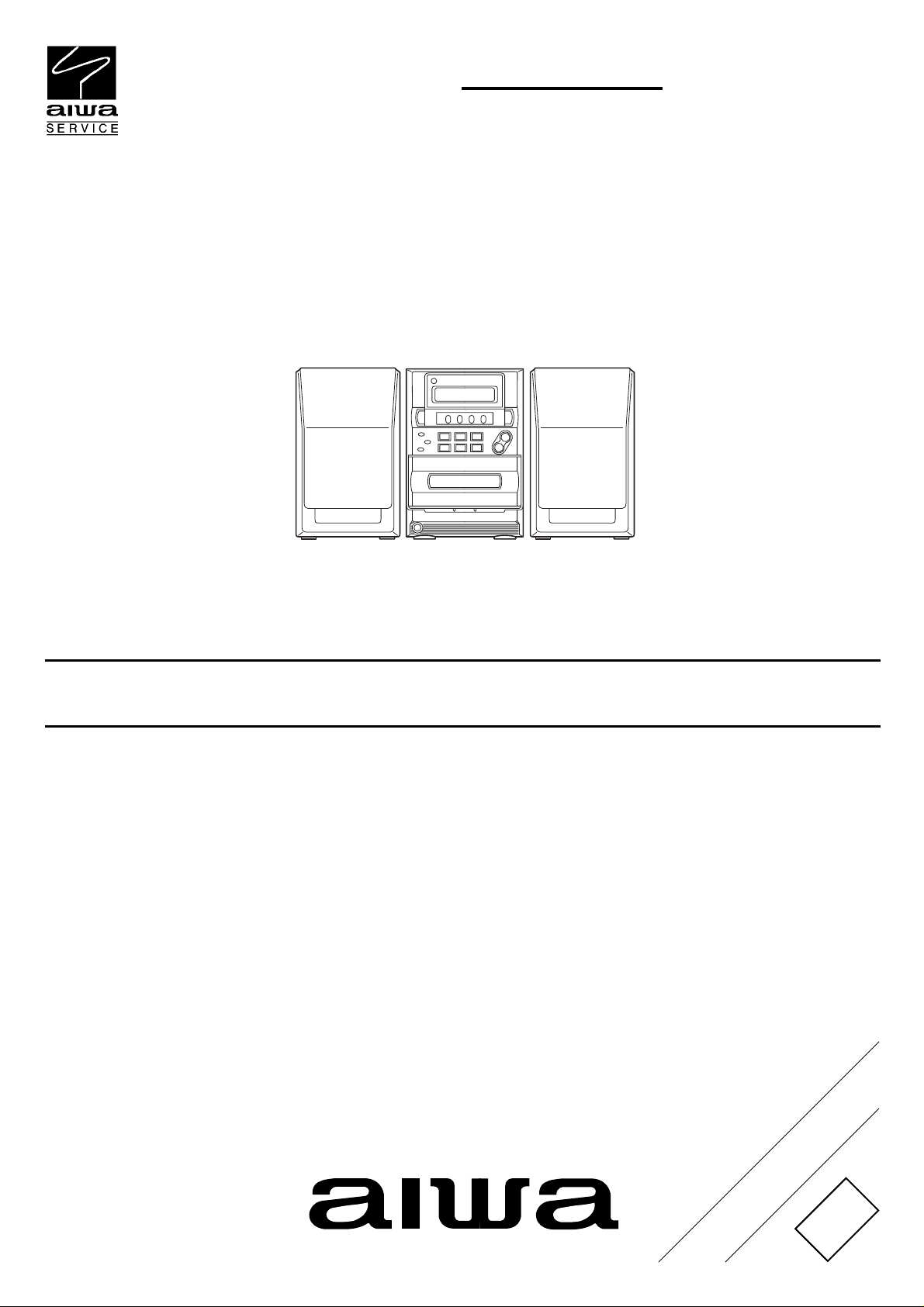
LCX-337
LH(S)
SERVICE MANUAL
COMPACT DISC STEREO
SYSTEM
This Service Manual is the "Revision Publishing" and replaces "Simple Manual"
(S/M Code No. 09-003-340-0T1).
BASIC TAPE MECHANISM : 2ZM-1YR8N
BASIC CD MECHANISM : DA11T3C
S/M Code No. 09-003-340-0R1
REVISION
DATA
Page 2
SPECIFICATIONS
Design and specifications are subject to change without
•
notice.
2
Page 3
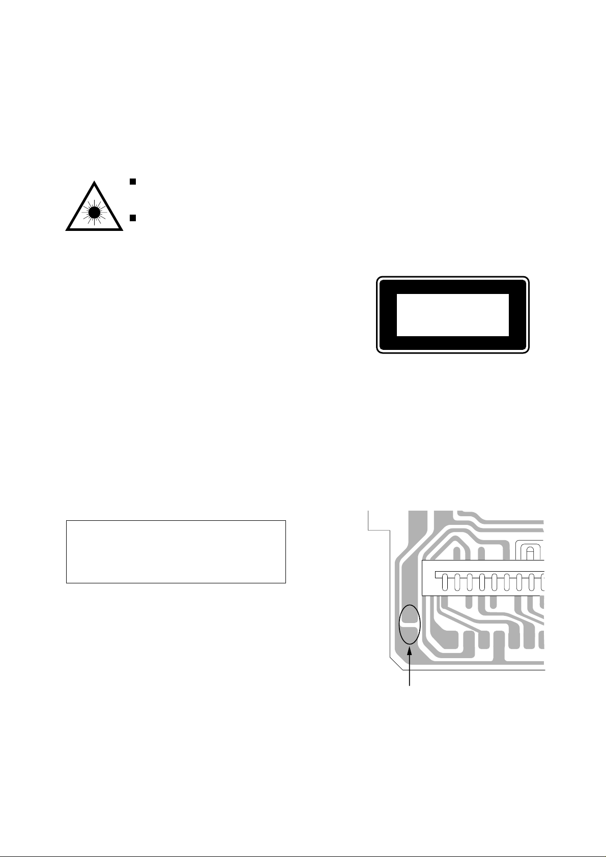
PROTECTION OF EYES FROM LASER BEAM DURING SERVICING
CLASS 1
KLASSE 1
LUOKAN 1
KLASS 1
LASER PRODUCT
LASER PRODUKT
LASER LAITE
LASER APPARAT
This set employs laser. Therefore, be sure to follow carefully the
instructions below when servicing.
WARNING!
WHEN SERVICING, DO NOT APPROACH THE LASER EXIT
WITH THE EYE TOO CLOSELY. IN CASE IT IS NECESSARY TO
CONFIRM LASER BEAM EMISSION. BE SURE TO OBSERVE
FROM A DISTANCE OF MORE THAN 30cm FROM THE
SURFACE OF THE OBJECTIVE LENS ON THE OPTICAL
PICK-UP BLOCK.
Caution: Invisible laser radiation when
open and interlocks defeated avoid exposure to beam.
Advarsel:Usynling laserståling ved åbning,
når sikkerhedsafbrydere er ude af funktion.
Undgå udsættelse for stråling.
VAROITUS!
Laiteen Käyttäminen muulla kuin tässä käyttöohjeessa mainitulla tavalla saattaa altistaa käyt-täjän turvallisuusluokan 1 ylittävälle näkymättömälle lasersäteilylle.
CAUTION
Use of controls or adjustments or performance of procedures
other than those specified herein may result in hazardous
radiation exposure.
ATTENTION
L'utilisation de commandes, réglages ou procédures autres que
ceux spécifiés peut entraîner une dangereuse exposition aux
radiations.
ADVARSEL!
Usynlig laserståling ved åbning, når sikkerhedsafbrydereer ude
af funktion. Undgå udsættelse for stråling.
This Compact Disc player is classified as a CLASS 1 LASER
product.
The CLASS 1 LASER PRODUCT label is located on the rear
exterior.
VARNING!
Om apparaten används på annat sätt än vad som specificeras i
denna bruksanvising, kan användaren utsättas för osynling
laserstrålning, som överskrider gränsen för laserklass 1.
Precaution to replace Optical block
(SF-P101NR)
Body or clothes electrostatic potential could ruin
laser diode in the optical block. Be sure ground
body and workbench, and use care the clothes
do not touch the diode.
1) After the connection, remove solder shown in
the right figure.
PICK-UP Assy P.C.B
Solder
3
Page 4

ELECTRICAL MAIN PARTS LIST
REF. NO PART NO. KANRI DESCRIPTION
NO.
IC
87-020-454-010 IC,DN6851
87-A20-734-010 IC,TDA2007A
87-A21-443-040 C-IC,M62495AFP
8A-CLA-620-010 IC,LC867240A-5P33
87-A21-245-010 IC,RPM6938-V4
87-A21-145-040 C-IC,BA4560F-E2
87-A20-446-010 C-IC,LA9241ML
87-A20-459-010 C-IC,LC78622ED
87-A21-093-010 IC,LA6541D
87-070-127-110 IC,LC72131 D
87-A20-913-010 IC,LA1837NL
TRANSISTOR
87-026-610-080 TR,KTC3198GR
89-213-702-010 TR,2SB1370 (1.8W)
87-A30-185-010 TR,2SD1381FQR
87-026-313-080 TR,DTC343TS
87-026-609-080 TR,KTA1266GR
87-026-218-080 TR,DTC144ES (0.2W)
87-026-237-080 CHIP-TR,DTC124XK
87-026-223-080 TR,DTC143TK
89-320-011-080 TR,2SC2001 (15W)
89-112-965-080 TR,2SA1296 (0.75W)
89-109-521-080 TR,2SA952 (0.6W)
87-A30-091-080 FET,2SJ460
87-A30-090-080 FET,2SK2541
87-A30-151-080 TR,2SA1993F
89-333-317-080 TR,2SC3331 (0.5W)
87-026-291-080 TR,DTC124XS
87-A30-227-080 TR,2SB1010Q
87-026-463-080 TR,2SA933S (0.3W)
87-026-210-080 CHIP-TR,DTC144EK
87-026-239-080 TR,DTC114TK (0.2W)
87-A30-196-080 TR,2SC4115SRS
89-327-143-080 TR,2SC2714 (0.1W)
87-A30-072-080 C-TR,RT1P 144C
DIODE
87-020-465-080 DIODE,1SS133 (110MA)
87-A40-393-090 DIODE,1N5402GW(F20)
87-070-334-080 ZENER,MTZJ10B
87-017-932-080 ZENER,MTJ6.2B
87-A40-347-080 ZENER,MTZJ2.2B
87-070-136-080 ZENER,MTZJ5.1B
87-020-027-080 CHIP-DIODE 1SS184
87-027-825-080 ZENER,HZ9A3L
MAIN C.B
C101 87-010-190-080 S CHIP F 0.01
C102 87-010-190-080 S CHIP F 0.01
C103 87-010-190-080 S CHIP F 0.01
C104 87-010-404-080 CAP, ELECT 4.7-50V
C105 87-010-403-080 CAP, ELECT 3.3-50V
C106 87-010-192-080 C-CAP,S 0.022-50 F
C107 87-010-192-080 C-CAP,S 0.022-50 F
C108 87-010-192-080 C-CAP,S 0.022-50 F
C109 87-010-192-080 C-CAP,S 0.022-50 F
C110 87-010-190-080 S CHIP F 0.01
C111 87-016-658-090 CAP,E 4700-35 SMG
C112 87-012-140-080 CAP 470P
C113 87-010-197-080 CAP, CHIP 0.01 DM
C114 87-010-408-080 CAP, ELECT 47-50V
C115 87-010-112-080 CAP, ELECT 100-16V
C116 87-010-101-080 CAP, ELECT 220-16
C118 87-010-263-080 CAP, ELECT 100-10V
REF. NO PART NO. KANRI DESCRIPTION
NO.
C119 87-010-190-080 S CHIP F 0.01
C120 87-010-401-080 CAP, ELECT 1-50V
C121 87-010-401-080 CAP, ELECT 1-50V
C122 87-010-213-080 C-CAP,S 0.015-50 B
C123 87-010-196-080 CHIP CAPACITOR,0.1-25
C124 87-010-402-080 CAP, ELECT 2.2-50V
C125 87-010-402-080 CAP, ELECT 2.2-50V
C126 87-010-408-080 CAP, ELECT 47-50V
C127 87-010-248-080 CAP, ELECT 220-10V
C128 87-010-393-080 CAP, ELECT 100-35V
C129 87-010-248-080 CAP, ELECT 220-10V
C130 87-010-393-080 CAP, ELECT 100-35V
C131 87-010-393-080 CAP, ELECT 100-35V
C132 87-010-237-080 CAP, ELECT 1000-16V
C133 87-010-237-080 CAP, ELECT 1000-16V
C136 87-010-197-080 CAP, CHIP 0.01 DM
C137 87-010-197-080 CAP, CHIP 0.01 DM
C138 87-010-197-080 CAP, CHIP 0.01 DM
C139 87-010-197-080 CAP, CHIP 0.01 DM
C143 87-010-401-080 CAP, ELECT 1-50V
C144 87-010-401-080 CAP, ELECT 1-50V
C147 87-010-190-080 S CHIP F 0.01
C150 87-010-263-080 CAP, ELECT 100-10V
C151 87-010-263-080 CAP, ELECT 100-10V
C152 87-010-182-080 C-CAP,S 2200P-50 B
C153 87-010-166-080 C-CAP,S 100P-50 SL
C154 87-010-545-080 CAP, ELECT 0.22-50V
C155 87-010-545-080 CAP, ELECT 0.22-50V
C157 87-010-404-080 CAP, ELECT 4.7-50V
C158 87-010-545-080 CAP, ELECT 0.22-50V
C159 87-010-545-080 CAP, ELECT 0.22-50V
C161 87-010-404-080 CAP, ELECT 4.7-50V
C162 87-010-405-080 CAP, ELECT 10-50V
C163 87-010-405-080 CAP, ELECT 10-50V
C164 87-010-405-080 CAP, ELECT 10-50V
C165 87-010-405-080 CAP, ELECT 10-50V
C166 87-010-404-080 CAP, ELECT 4.7-50V
C167 87-010-404-080 CAP, ELECT 4.7-50V
C171 87-010-404-080 CAP, ELECT 4.7-50V
C172 87-010-408-080 CAP, ELECT 47-50V
C173 87-010-405-080 CAP, ELECT 10-50V
C175 87-010-237-080 CAP, ELECT 1000-16V
C300 87-010-986-080 C-CAP,S 820P-50 J CH
C301 87-010-198-080 CAP, CHIP 0.022
C302 87-010-986-080 C-CAP,S 820P-50 J CH
C303 87-010-180-080 C-CER 1500P
C304 87-010-180-080 C-CER 1500P
C305 87-010-263-080 CAP, ELECT 100-10V
C306 87-010-263-080 CAP, ELECT 100-10V
C307 87-010-956-080 CHIP-CAP,S 0.068-25B
C308 87-010-956-080 CHIP-CAP,S 0.068-25B
C309 87-010-187-080 CAP CHIP S5600P
C310 87-010-187-080 CAP CHIP S5600P
C311 87-010-374-080 CAP, ELECT 47-10V
C312 87-010-546-080 CAP, ELECT 0.33-50V
C313 87-010-546-080 CAP, ELECT 0.33-50V
C314 87-010-401-080 CAP, ELECT 1-50V
C315 87-010-401-080 CAP, ELECT 1-50V
C316 87-010-182-080 C-CAP,S 2200P-50 B
C317 87-010-182-080 C-CAP,S 2200P-50 B
C318 87-010-188-080 CAP,CHIP 6800P
C319 87-010-188-080 CAP,CHIP 6800P
C320 87-010-184-080 CHIP CAPACITOR 3300P(K)
C321 87-010-184-080 CHIP CAPACITOR 3300P(K)
C322 87-010-321-080 CHIP CAPACITOR,82P(J)
C323 87-010-321-080 CHIP CAPACITOR,82P(J)
C324 87-010-401-080 CAP, ELECT 1-50V
C325 87-010-374-080 CAP, ELECT 47-10V
C326 87-010-198-080 CAP, CHIP 0.022
C327 87-010-183-080 C-CAP,S 2700P-50 B
4
Page 5

REF. NO PART NO. KANRI DESCRIPTION
NO.
C328 87-010-183-080 C-CAP,S 2700P-50 B
C329 87-010-183-080 C-CAP,S 2700P-50 B
C331 87-010-382-080 CAP, ELECT 22-25V
C332 87-010-187-080 CAP CHIP S5600P
C333 87-010-178-080 CHIP CAP 1000P
C334 87-010-175-080 CAP 560P
C335 87-012-158-080 C-CAP,S 390P-50 CH
C336 87-012-158-080 C-CAP,S 390P-50 CH
C337 87-010-198-080 CAP, CHIP 0.022
C701 87-010-381-080 CAP, ELECT 330-16V
C702 87-010-404-080 CAP, ELECT 4.7-50V
C703 87-012-286-080 CAP, U 0.01-25
C704 87-012-286-080 CAP, U 0.01-25
C709 87-012-195-080 C-CAP,U 100P-50CH
C711 87-010-263-080 CAP, ELECT 100-10V
C712 87-010-831-080 C-CAP,U,0.1-16F
C714 87-012-286-080 CAP, U 0.01-25
C719 87-012-286-080 CAP, U 0.01-25
C720 87-012-195-080 C-CAP,U 100P-50CH
C721 87-012-176-080 CAP 15P
C722 87-012-176-080 CAP 15P
C723 87-012-274-080 CHIP CAP,U 1000P-50B
C725 87-012-274-080 CHIP CAP,U 1000P-50B
C727 87-010-196-080 CHIP CAPACITOR,0.1-25
C728 87-010-248-080 CAP, ELECT 220-10V
C729 87-012-274-080 CHIP CAP,U 1000P-50B
C731 87-012-286-080 CAP, U 0.01-25
C756 87-012-286-080 CAP, U 0.01-25
C757 87-012-188-080 C-CAP,U 47P-50 CH
C758 87-012-167-080 C-CAP,U 5P-50 CH
C763 87-010-829-080 CAP, U 0.047-16
C764 87-012-337-080 C-CAP,U 56P-50 CH
C765 87-012-286-080 CAP, U 0.01-25
C768 87-012-286-080 CAP, U 0.01-25
C769 87-010-260-080 CAP, ELECT 47-25V
C770 87-010-829-080 CAP, U 0.047-16
C771 87-010-383-080 CAP, ELECT 33-25V
C772 87-010-829-080 CAP, U 0.047-16
C773 87-010-196-080 CHIP CAPACITOR,0.1-25
C774 87-010-263-080 CAP, ELECT 100-10V
C775 87-010-404-080 CAP, ELECT 4.7-50V
C776 87-012-286-080 CAP, U 0.01-25
C777 87-010-400-080 CAP, ELECT 0.47-50V
C778 87-010-401-080 CAP, ELECT 1-50V
C779 87-010-401-080 CAP, ELECT 1-50V
C780 87-010-196-080 CHIP CAPACITOR,0.1-25
C781 87-010-405-080 CAP, ELECT 10-50V
C782 87-010-405-080 CAP, ELECT 10-50V
C783 87-012-286-080 CAP, U 0.01-25
C784 87-012-286-080 CAP, U 0.01-25
C785 87-010-401-080 CAP, ELECT 1-50V
C786 87-010-401-080 CAP, ELECT 1-50V
C789 87-012-275-080 C-CAP,U 1200P-50 B
C790 87-012-275-080 C-CAP,U 1200P-50 B
C791 87-010-405-080 CAP, ELECT 10-50V
C793 87-012-273-080 C-CAP,U 820P-50 B
C794 87-010-406-080 CAP, ELECT 22-50
C795 87-010-596-080 CAP, S 0.047-16
C796 87-010-403-080 CAP, ELECT 3.3-50V
C797 87-012-278-080 C-CAP,U 2200P-50 B
C798 87-012-278-080 C-CAP,U 2200P-50 B
C799 87-010-829-080 CAP, U 0.047-16
C812 87-012-286-080 CAP, U 0.01-25
C820 87-010-260-080 CAP, ELECT 47-25V
C821 87-012-286-080 CAP, U 0.01-25
C822 87-012-286-080 CAP, U 0.01-25
C823 87-012-286-080 CAP, U 0.01-25
C828 87-010-196-080 CHIP CAPACITOR,0.1-25
C829 87-010-196-080 CHIP CAPACITOR,0.1-25
C959 87-010-831-080 C-CAP,U,0.1-16F
REF. NO PART NO. KANRI DESCRIPTION
C960 87-010-196-080 CHIP CAPACITOR,0.1-25
C961 87-012-170-080 C-CAP,U 8P-50 CH
C963 87-010-196-080 CHIP CAPACITOR,0.1-25
CF801 87-008-261-010 FILTER, SFE10.7MA5-A
CF802 87-008-261-010 FILTER, SFE10.7MA5-A
CON301 87-099-832-010 CONN,8P S2M-8W
!
F101 87-035-457-010 FUSE,3.15A 250V TW/C
!
FC101 87-033-213-080 CLAMP, FUSE
!
FC102 87-033-213-080 CLAMP, FUSE
FFE801 A8-8ZA-193-070 8ZA-1 YFEUNC
J101 8A-CLA-624-010 JACK,PIN 3P AUX
J102 87-A60-754-010 TERMINAL,SPK 4P MSP-154V-05
J103 87-A60-420-010 JACK,3.5 ST (MSC)
J801 87-A60-202-010 TERMINAL,ANT 4P MSP-154V-02
L101 87-005-366-010 COIL, 1UH
L102 87-005-366-010 COIL, 1UH
L104 87-005-676-080 COIL,2.2UH K LF5.0S
L302 87-007-342-010 COIL,OSC 85K BIAS
L771 87-A50-266-010 COIL,FM DET-2N(TOK)
L772 87-A90-733-010 FLTR,PCFAZH-450 (TOK)
L773 87-NF4-650-010 COIL,AM PACK 4N(TOK)
PR100 87-A90-091-080 PROTECTOR,2A 491
PR101 87-026-689-080 PROTECTOR,1A 60V 491
R118 87-029-118-090 RES,FUSE 220-1/2W J
R362 87-029-090-010 RES FUSE,22-1/4
R503 87-029-019-010 RES, FUSEIBLE 1/2W-2.2
WH101 87-099-043-010 CONN 2P EH
X721 87-A70-061-010 VIB,XTAL 4.500MHZ CSA-309
FRONT C.B
C201 87-010-375-080 CAP,E 330-10 SME
C202 87-012-350-080 C-CAP,1-25 F
C203 87-010-197-080 CAP, CHIP 0.01 DM
C205 87-010-178-080 CHIP CAP 1000P
C208 87-010-197-080 CAP, CHIP 0.01 DM
C209 87-010-196-080 CHIP CAPACITOR,0.1-25
C210 87-010-196-080 CHIP CAPACITOR,0.1-25
C211 87-010-314-080 C-CAP,S 22P-50V
C212 87-010-318-080 C-CAP,S 47P-50 CH
C213 87-010-154-080 CAP CHIP 10P
C214 87-012-149-080 C-CAP,S 30P-50 CH
C215 87-010-312-080 C-CAP,S 15P-50 CH
C216 87-010-400-080 CAP, ELECT 0.47-50V
C217 87-010-196-080 CHIP CAPACITOR,0.1-25
CN201 87-099-720-010 CONN,30P TYK-B(P)
CN202 87-A60-404-010 CONN,3P TKX-P03P-F1
CN203 8A-CLA-621-010 CONN ASSY,9P MOTOR
L206 87-003-098-080 COIL,2.2UH
LCD201 8Z-CL8-665-110 LCD,ZCL-8
S200 87-A90-095-080 SW,TACT EVQ11G04M
S201 87-A90-095-080 SW,TACT EVQ11G04M
S202 87-A90-095-080 SW,TACT EVQ11G04M
S203 87-A90-095-080 SW,TACT EVQ11G04M
S204 87-A90-095-080 SW,TACT EVQ11G04M
S205 87-A90-095-080 SW,TACT EVQ11G04M
S206 87-A90-095-080 SW,TACT EVQ11G04M
S207 87-A90-095-080 SW,TACT EVQ11G04M
S208 87-A90-095-080 SW,TACT EVQ11G04M
S209 87-A90-095-080 SW,TACT EVQ11G04M
S214 87-A90-095-080 SW,TACT EVQ11G04M
S215 87-A90-095-080 SW,TACT EVQ11G04M
S216 87-A90-095-080 SW,TACT EVQ11G04M
S217 87-A90-095-080 SW,TACT EVQ11G04M
S218 87-A90-095-080 SW,TACT EVQ11G04M
S219 87-A90-095-080 SW,TACT EVQ11G04M
S220 87-A90-095-080 SW,TACT EVQ11G04M
X201 87-030-364-010 VIB,XTAL 32.768K CT
X202 87-A70-185-080 VIB,CER 5.76MHZ TF21
NO.
5
Page 6

REF. NO PART NO. KANRI DESCRIPTION
NO.
CD C.B
C500 87-016-459-040 CAP,E 470-10 SMG
C502 87-016-459-040 CAP,E 470-10 SMG
C503 87-016-459-040 CAP,E 470-10 SMG
C505 87-010-196-080 CHIP CAPACITOR,0.1-25
C507 87-010-196-080 CHIP CAPACITOR,0.1-25
C510 87-010-197-080 CAP, CHIP 0.01 DM
C513 87-010-196-080 CHIP CAPACITOR,0.1-25
C514 87-010-196-080 CHIP CAPACITOR,0.1-25
C515 87-012-157-080 C-CAP,S 330P-50 CH
C516 87-010-545-080 CAP, ELECT 0.22-50V
C525 87-010-176-080 C-CAP,S 680P-50 SL
C528 87-012-156-080 C-CAP,S 220P-50 CH
C529 87-010-545-080 CAP, ELECT 0.22-50V
C530 87-012-140-080 CAP 470P
C531 87-010-374-080 CAP, ELECT 47-10V
C532 87-010-401-080 CAP, ELECT 1-50V
C533 87-010-184-080 CHIP CAPACITOR 3300P(K)
C535 87-010-145-080 C-CAP,S 1P-50 CH
C536 87-010-312-080 C-CAP,S 15P-50 CH
C537 87-010-166-080 C-CAP,S 100P-50 SL
C538 87-010-196-080 CHIP CAPACITOR,0.1-25
C539 87-010-404-080 CAP, ELECT 4.7-50V
C540 87-010-196-080 CHIP CAPACITOR,0.1-25
C541 87-010-405-080 CAP, ELECT 10-50V
C542 87-010-369-080 C-CAP,S 0.033-25 K B
C545 87-010-197-080 CAP, CHIP 0.01 DM
C546 87-010-401-080 CAP, ELECT 1-50V
C546 87-010-374-080 CAP, ELECT 47-10V
C547 87-010-263-080 CAP, ELECT 100-10V
C548 87-010-248-080 CAP, ELECT 220-10V
C549 87-010-198-080 CAP, CHIP 0.022
C550 87-010-248-080 CAP, ELECT 220-10V
C551 87-010-166-080 C-CAP,S 100P-50 SL
C552 87-010-197-080 CAP, CHIP 0.01 DM
C553 87-010-374-080 CAP, ELECT 47-10V
C555 87-010-403-080 CAP, ELECT 3.3-50V
C556 87-010-197-080 CAP, CHIP 0.01 DM
C557 87-010-197-080 CAP, CHIP 0.01 DM
C558 87-010-197-080 CAP, CHIP 0.01 DM
C559 87-010-315-080 C-CAP,S 27P-50 CH
C560 87-010-263-080 CAP, ELECT 100-10V
C561 87-010-196-080 CHIP CAPACITOR,0.1-25
C562 87-010-196-080 CHIP CAPACITOR,0.1-25
C563 87-012-156-080 C-CAP,S 220P-50 CH
C565 87-010-263-080 CAP, ELECT 100-10V
C566 87-010-196-080 CHIP CAPACITOR,0.1-25
C568 87-010-197-080 CAP, CHIP 0.01 DM
C570 87-010-197-080 CAP, CHIP 0.01 DM
C571 87-010-248-080 CAP, ELECT 220-10V
C572 87-010-196-080 CHIP CAPACITOR,0.1-25
C573 87-010-197-080 CAP, CHIP 0.01 DM
C574 87-010-197-080 CAP, CHIP 0.01 DM
C578 87-010-197-080 CAP, CHIP 0.01 DM
C579 87-010-263-080 CAP, ELECT 100-10V
C582 87-010-197-080 CAP, CHIP 0.01 DM
REF. NO PART NO. KANRI DESCRIPTION
NO.
C583 87-010-405-080 CAP, ELECT 10-50V
C584 87-010-170-080 S CHIP SL 220P(K)
C586 87-010-170-080 S CHIP SL 220P(K)
C587 87-010-166-080 C-CAP,S 100P-50 SL
C589 87-010-166-080 C-CAP,S 100P-50 SL
C590 87-010-166-080 C-CAP,S 100P-50 SL
C591 87-010-166-080 C-CAP,S 100P-50 SL
C592 87-010-166-080 C-CAP,S 100P-50 SL
C593 87-010-197-080 CAP, CHIP 0.01 DM
C594 87-010-263-080 CAP, ELECT 100-10V
C596 87-010-404-080 CAP, ELECT 4.7-50V
C597 87-010-197-080 CAP, CHIP 0.01 DM
C598 87-010-197-080 CAP, CHIP 0.01 DM
C601 87-010-197-080 CAP, CHIP 0.01 DM
CN501 87-009-345-010 CONN,2P PH H
CN510 87-009-034-010 CONN,6P PH V
CN520 87-A60-248-010 CONN,16P H CFF1416
L501 87-005-647-080 COIL,10UH K LF5S
L502 87-005-659-080 COIL,100UH K LF5.0S
SFR501 87-A90-787-080 SFR,100K H HOKU
X501 87-A70-046-010 VIB,XTAL 16.934MHZ
LED C.B
D941 87-A40-365-080 LED,L-1154 SGD
D942 87-A40-365-080 LED,L-1154 SGD
D943 87-A40-365-080 LED,L-1154 SGD
D944 87-A40-365-080 LED,L-1154 SGD
D945 87-A40-365-080 LED,L-1154 SGD
D946 87-A40-365-080 LED,L-1154 SGD
D947 87-A40-365-080 LED,L-1154 SGD
D948 87-A40-365-080 LED,L-1154 SGD
D949 87-A40-365-080 LED,L-1154 SGD
AC C.B
CNA101 8A-CLA-630-010 CONN ASSY,2P PT
SW1 87-A90-178-010 SW SL1-1-2
T1 87-A60-317-010 TERMINAL, 1P MSC
T2 87-A60-317-010 TERMINAL, 1P MSC
MOTOR C.B
M2 9X-262-576-910 MOTOR GEAR ASSY
PIN3 91-564-722-110 CONNECTOR 6P
SW1 91-572-085-120 LEAF SW
DECK C.B
CN1 87-009-352-010 CONN,9P PH H
SFR1 87-024-581-010 SFR,3.3K DIA6V K0A
SOL2 82-ZM1-618-410 SOL ASSY,27K
SW2 87-A90-248-010 SW,MICRO ESE11SH2CXQ
SW3 87-A90-248-010 SW,MICRO ESE11SH2CXQ
SW5 87-A90-248-010 SW,MICRO ESE11SH2CXQ
SW6 87-A90-248-010 SW,MICRO ESE11SH2CXQ
RELAY C.B
• Regarding connectors, they are not stocked as they are not the initial order items.
The connectors are available after they are supplied from connector manufacturers upon the order is received.
6
Page 7
CHIP RESISTOR PART CODE
Chip Resistor Part Coding
88
FL (13-ST-36GNAK) GRID ASSIGNMENT/ANODE CONNECTION
GRID ASSIGNMENT
A
Resistor Code
Chip resistor
Wattage Type Tolerance
1/16W 1005 5% CJ
1/16W
1/10W
1/8W
1608
2125
3216
5%
5%
5%
TRANSISTOR ILLUSTRATION
Symbol
CJ
CJ
CJ
Figure
Value of resistor
Form
L
Dimensions (mm)
t
W
0.55
Resistor Code
108
118
128
LW t
1.0 0.5 0.35 104
1.6 0.8 0.45
2 1.25 0.45
3.2
1.6
: A
: A
ANODE CONNECTION
C
B
E
2SC2714
2SD1306
DTC114TK
DTC143TK
DTC144EK
RT1P141C
PT1P144C
ECB ECB ECB ECB
2SA1296
2SC1815
KTC3198
2SC4115
DTC124XS
DTC343TS
2SA933
2SB1010
2SC2001
2SD1381
SS8050
G
S
D
2SK543
87
Page 8
WIRING-1 (MAIN)
1
234567
8
9
10
11 12 13
14
A
MAIN C.B
B
J102
SPEAKERS
R
(INSERTED PARTS)
PHONES
19
MAIN C.B
J103
5
8
C
L
D
J101
L
AUX
R
SUPER
E
WOOFER
123
1
8
(CHIP PARTS)
4
1
5
4
8
1
1324
112
J801
11
F
AM LOOP
ANTENNA
FM
75Ω
12 22
1
1630
115
30
29
G
12345678
TO FRONT C.B CN201
2
1
H
AC C.B
NOTE
I
(INSERTED PARTS)
2
1
PT101
POWER TRANSFORMER
RELAY C.B
AC VOLTAGE
SELECTOR
J
ECB
ECB
ECB
120V
220-240V
K
109
Page 9
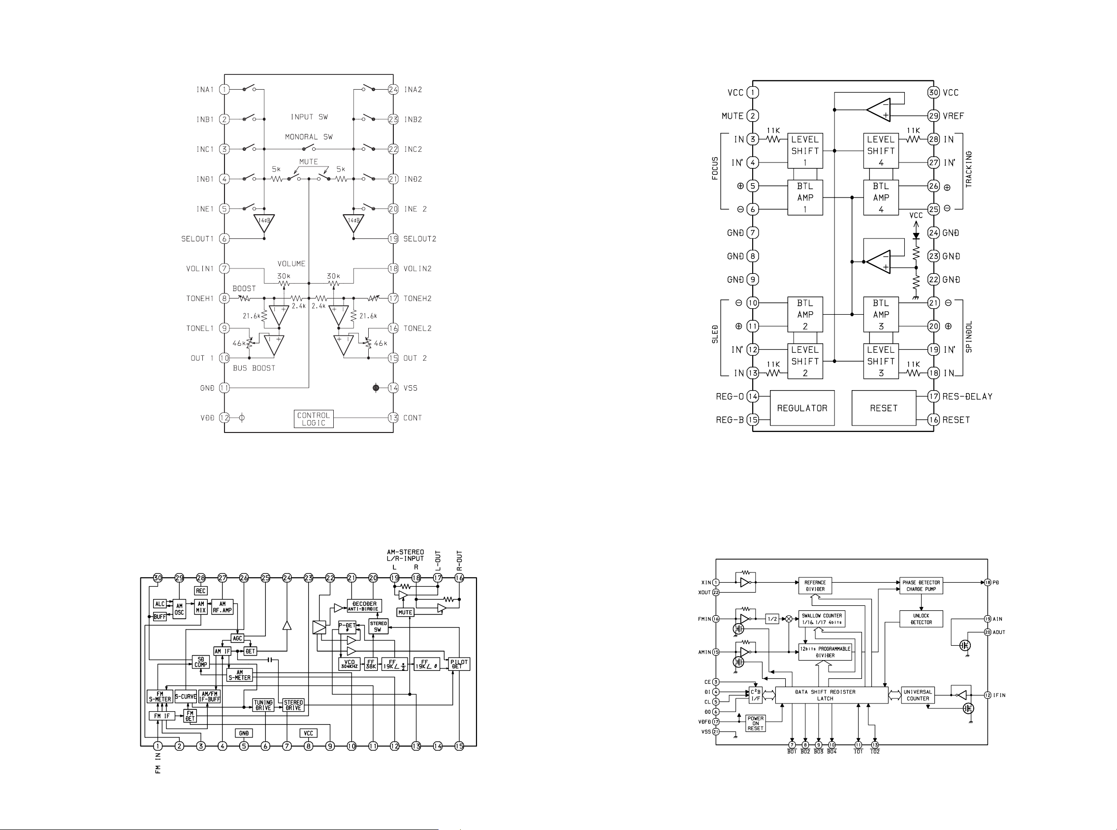
IC BLOCK DIAGRAM
IC, M62495AFP
IC, LA6541D
IC, LA1837NL IC, LC72131D
1211
Page 10
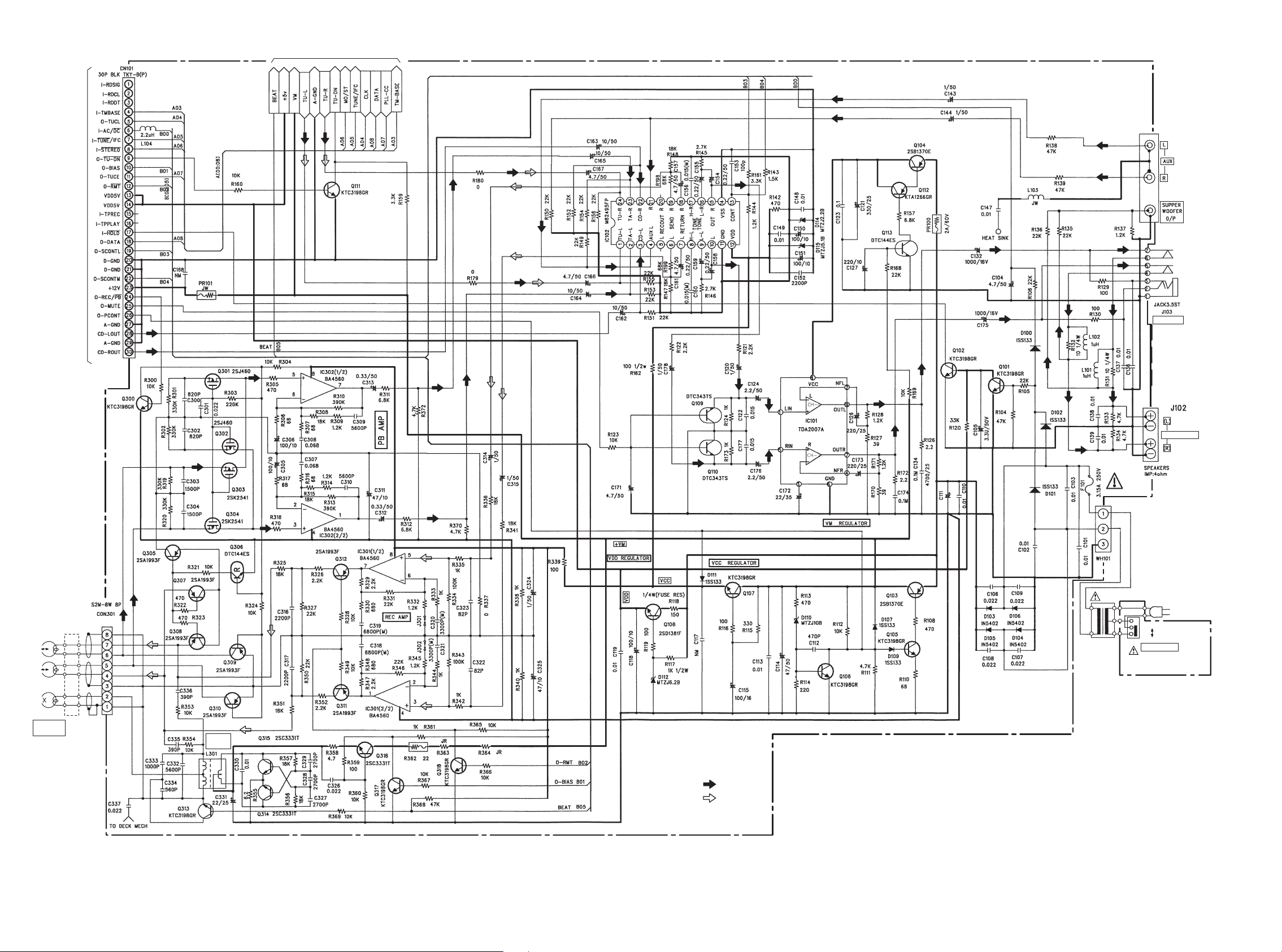
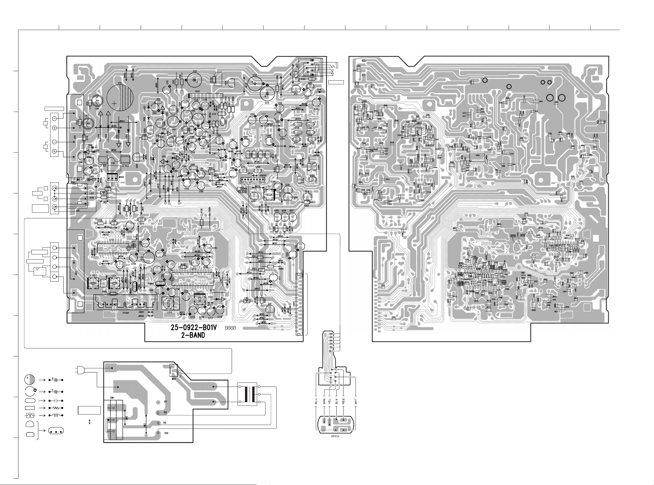
SCHEMATIC DIAGRAM-1 (MAIN 1/2)
MAIN C.B (1/2)
TO MAIN C.B 2/2
REG
J101
HEADPHONES
JACK. PIN 2P MSP
TO FRONT C.B CN201
INV.
Q301,302,303,304
REC/PB SW
INV.
IC201
FUNCTION
SWITCH
MAIN MUITE
Q109/Q110
POWER AMP
REG
SW
R
PHONES
HOLD DET
HOLD DET
SPEAKERS
RCH
LCH
EH
AZIMUTH
ADJ
Q305,307,308
REC/PB SW
BEAT CUT
REC/PB SW
REC/PB SW
AC BIAS
ADJ
INV.
BIAS OSC
RMT SW
BIAS OSC
RMT SW
REG
Q108
Q107
REG
REG
REG
SW
PT101
SW1
AC
120V
220-240V
AC VOLTAGE
120/220-240V
50/60Hz
AC C.B
POWER
CONT
SW
INV.
SIGNAL
: PB/FM
: REC/AM
1413
Page 11
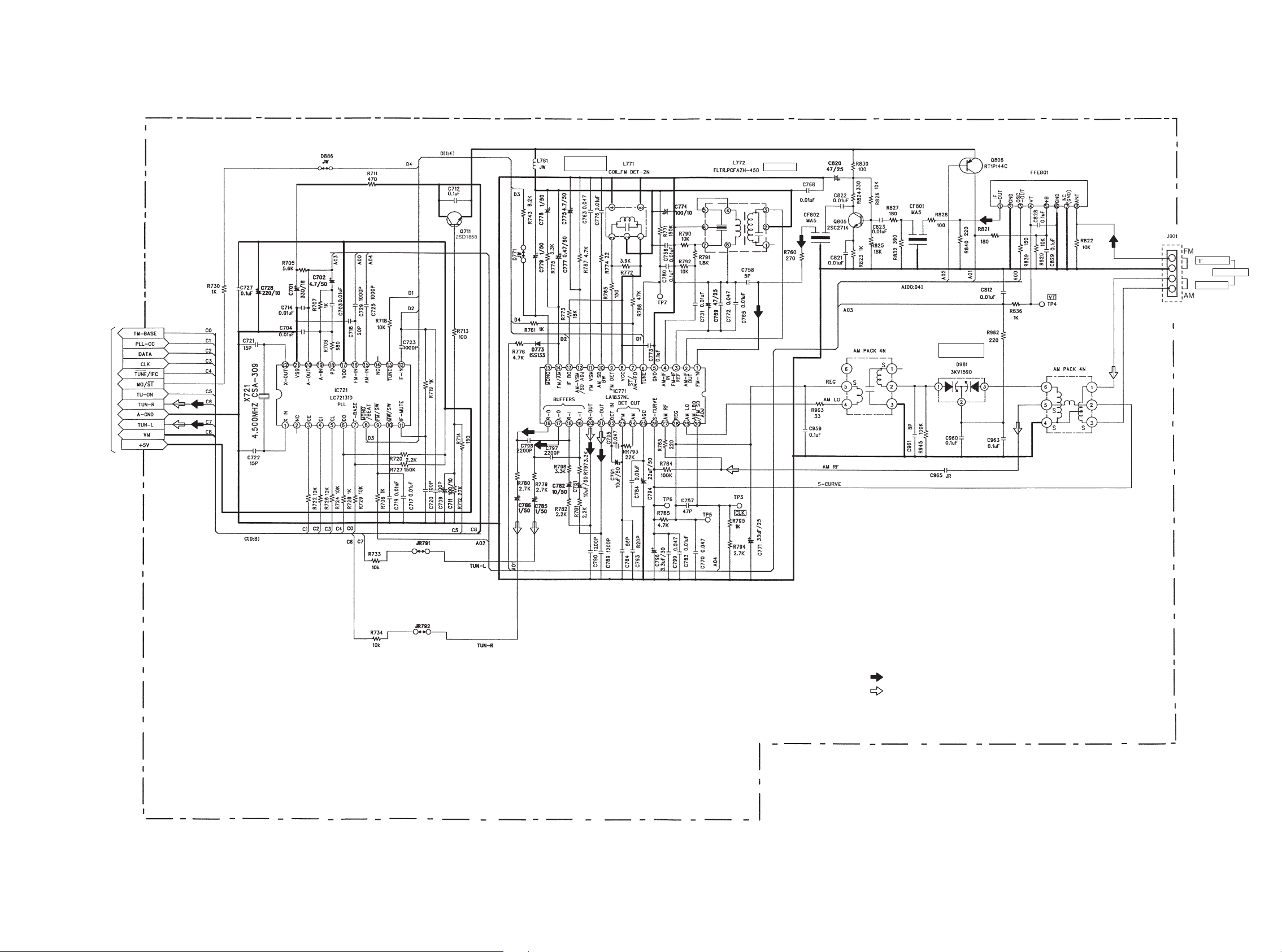
SCHEMATIC DIAGRAM-2 (MAIN 2/2)
MAIN C.B (2/2)
TUNER
ON/OFF
SWITCH
DC BALANCE
ADJ
AM IF ADJ
IF AMP
R
BAND SW
FM FRONTEND
PACK 8ZA-1 YFEUNC
TO MAIN C.B (1/2)
IC771
FM/AM IF/STEREO
TUNER SYSTEM
L774
AM TRACKING
ADJ
L773
1
2
3
4
FM 75Ω
ANTENNA
AM LOOP
SIGNAL
: PB/FM
: REC/AM
1615
Page 12

WIRING-2 (CD FRONT: INSERTED PARTS)
1
234567
8
9
10
11 12 13
14
FRONT C.B
A
(INSERTED PARTS)
1
3
(DISPLAY)
51015202530354043
1
CD C.B
(INSERTED PARTS)
B
1
2
31
C
TO MAIN C.B CN101
D
POWER
29
30
TAPE/
REV MODE
TUNER/
BAND
CD
AUX
TIMER/
SLEEP
2
1
16
15
2
1
S101
(DOOR SW)
E
F
G
H
ROCK
19
JAZZ
POP
/SET
REC/REC MUTE
DIR/
PRESET
LED C.B
13
CLEAR
VOLUME
(INSERTED PARTS)
16202530
15 15
10
16
DECK C.B
NOTE
I
Cxxx
Rxxx
J
ECB
ECB
K
1817
Page 13

WIRING-3 (CD FRONT: CHIP PARTS)
CD C.B (CHIP PARTS)
16
15
2
1
FRONT C.B (CHIP PARTS)
1
CN510
LED C.B (CHIP PARTS)
MOTOR C.B
M2
6
+
_
OPTICAL
PICK UP
SF-P101NR
NOTE
C
B
E
SW1
C
E
B
2019
PIN3
M2
(SLED MOTOR)
(INSIDE LIMIT SW)
SW1
(SPINDLE MOTOR)
_
M3
M3
+
Page 14

SCHEMATIC DIAGRAM-3 (FRONT)
2221
Page 15

SCHEMATIC DIAGRAM-4 (CD)
2423
Page 16

VOLTAGE CHART
2625
Page 17

272829
Page 18

Page 19

Page 20

ELECTRICAL ADJUSTMENT
30
Page 21

DECK C.B
SFR1
1
DECK R/P/E HEAD
CON1
2
2
REV FWD
< DECK SECTION >
1. Tape Speed Adjustment
Settings: • Test tape: TTA-100
• Test point: SP-OUT 2V
• Adjustment location: SFR1
Method: Play back the test tape and adjust SFR1 for
3000Hz±5Hz (FWD) and FWD PLAY
speed±45Hz (REV).
2. Head Azimuth Adjustment
Settings: • Test tape: TTA-300
• Test point: SP-OUT 2V
• Adjustment location: Head azimuth
adjustment screw
Method: Play back the 8kHz signal of the test tape and
adjust screw so that the output becomes
maximum. Next, Perform on each FWD PLAY
and REV PLAY mode.
3. PB Frequency Response Check
Settings: • Test tape: TTA-320
• Test point: SP-OUT 2V
Method: Play back the 315Hz and 10kHz signals of the
test tape and check that the 10kHz signal with
respect to that of the 315Hz signal is 0dB±3dB.
4. REC/PB Frequency Response Check
Settings: • Test tape: TTA-602
• Test point: SP-OUT 2V
Method: Input a-20VU signal to the AUX terminal.
Record the 1kHz and 10kHz signals on the test
tape and play back them. Check that the
difference between the record level and the
play back level at 1kHz and 10kHz signal is
0dB to ±3dB.
PRACTICAL SERVICE FIGURE
< TUNER SECTION >
< FM SECTION >
IHF Sensitivity: 15dB±5dB (at 90.0MHz)
(THD 3%) 14dB±5dB (at 98.0/106.0MHz)
Signal to noise ratio: More than 60dB
(Input 54dB) (at 98.0MHz)
Distortion: Less than 1.2%
(Input 54dB) (at 98.0MHz)
Auto stop level: 25±10dB (at 98.0MHz)
Stereo separation: More than 20dB (at 98.0MHz)
Intermediate frequency: 10.75MHz
< AM (MW) SECTION >
Sensitivity: 46±5dB (at 600kHz)
(S/N 10dB) 44±5dB (at 1000kHz)
42±5dB (at 1400kHz)
Signal to noise ratio: More than 33dB
(Input 74dB) (at 999kHz)
Distortion: Less than 3.0%
(Input 74dB) (at 999kHz)
Auto stop level: 50+10/-15dB (at 1000kHz)
Intermediate frequency: 450kHz
< DECK SECTION >
Tape speed: 3000Hz±45%
Wow & flutter: Less than 0.14%
(W.R.M.S)
Pinch roller pressure: 270-330g
Take-up torque: 30-55g-cm (FWD, REV)
FF & REW torque: 75-180g-cm
Back tension: 2-7g-cm (FWD, REV)
Distortion: Less than 3.0%
(REC/PB, 0VU)
Noise level: Less than 80mV
(PB, REC/PB,
FILTER DIN AUDIO)
Erasing ratio: More than 55dB
(at 125Hz, +10VU)
Test tape: TTA-100
TTA-602 (NORMAL)
31
Page 22

IC DESCRIPTION
IC, LC867240A-5P33
Pin No. Pin Name I/O Description
1
2
3
4
5
6
7
8
9
10
11
12
13
O-SCONTM
O-SCONTL
O-DATA
___________
I-TUNE/IFC
O-TUCL
O-COIN
I-SQOUT
___________
O-CQCK
O-RWC
_______________
O-CLKSFT
I-TMBASE
____________
I-RESET
XT1
O
M62439SP control. open drain output.
O
O
Tuner control. CMOS output.
I
Tuner control.
O
Tuner control. CMOS output.
O
CD control. open drain output.
I
CD control.
O
CD control. open drain output.
O
O
Clock shift output. “L” during shift. open drain output.
I
8 Hz time base input.
I
Reset input.
I
Input pin.
14
15
16, 17
18
19
20
21
22
23
24
25
26
27
28
29
30
31
32
33
XT2
VSS1
CF1, CF2
VDD1
I-KEY0
I-KEY1
I-RDSIG
I-WRQ
I-DRF
I-DOOR
I-PUIN
I-SWTAPE
________________
I-STEREO
I-RDCL
________
I-REM
___________
I-HOLD
I-RDDT
I-TPREC
I-TPPLAY
O
—
I/O
—
Output pin for 32.768kHz crystal oscillation.
GND.
Main clock input/output 5.76 MHz.
+5V.
I
KEY0 A/D input.
I
KEY1 A/D input.
I
RDS signal level input. (A/D input)
I
CD control.
I
I
CD door SW detection SW input. “L” at CLOSE.
I
CD pick-up detection SW input. “L” at ON.
I
Tape detection SW input. (A/D input)
I
Monaural/stereo indication selector input. “L” at stereo.
I
RDS clock input.
I
Remote control input. (fall-down edge interrupt input)
I
Hold mode detection. “L” at hold mode.
I
RDS data input.
I
Tape REC detection input. “H” at REC.
I
Tape PLAY detection input. “H” at PLAY.
34
35
36-38
39-55
56
57
58-79
80
81
O-MOTOR
O-PL
O-NC
S9-S25
VDD2
VSS2
S26-S47
I-CLKDSP
I-AS
—
—
O
Mechanism deck motor ON/OFF output. “H” at ON. CMOS output.
O
Mechanism deck plunger solenoid ON/OFF output. “H” at ON. CMOS output .
O
Not used.
O
LCD SEG terminal Initial setting output. (S10 to S16)
+5V.
GND.
O
LCD SEG terminal .
I
Watch indication select input “L”: 12H. “H”: 24H.
I
Auto stop. counter input .
32
Page 23

Pin No. Pin Name I/O Description
__________
82
83-86
87
88
89
90
91
92
I-STOP
COM0-COM3
I-INIT
______
I-AC/DC
VSS3
VDD3
O-NC
O-TUCE
I
Tape stop input.
O
LCD common output.
I
Initial setting input.
O
Beat selector output. “H” during selection. CMOS output .
—
GND.
—
5V.
O
Not used.
O
Tuner chip enable output. CMOS output .
93
94
95
96
97
98
99
100
O-CD-ON
_____________
O-TU-ON
__________
O-RMT
________ _____
O-REC/PB
O-MUTE
O-PCONT
__________
O-BIAS
O-NC
O
“H” output during CD function. CMOS output.
O
“H” output during TU function. Open drain output.
O
REC mute output. “H” during mute. Open drain output.
O
REC/PB select output. “H” during PB. Open drain output.
O
Mute output. “H” during mute. Open drain output.
O
Power control output. “H” at ON. CMOS output.
O
REC bias ON/OFF output. “H” at ON. Open drain output.
O
Not used.
33
Page 24

IC, LA9241ML
Pin No. Pin Name I/O Description
1
2
FIN2
FIN1
Pin to which external pickup photo diode is connected. RF signal is created by adding
I
with the FIN1 pin signal. FE signal is created by subtracting from the FIN1 pin signal.
I
Pin to which external pickup photo diode is connected.
10
11
12
13
14
15
16
17
3
4
5
6
7
8
9
E
F
TB
TE–
TE
TESI
SCI
TH
TA
TD–
TD
JP
TO
FD
FD–
Pin to which external pickup photo diode is connected. TE signal is created by
I
subtracting from the F pin signal.
I
Pin to which external pickup photo diode is connected.
I
DC component of the TE signal is input.
I
Pin to which external resistor setting the TE signal gain is connected between the TE pin.
O
TE signal output pin.
TES “Track Error Sense” comparator input pin. TE signal is passed through a band-
I
pass filter then input.
I
Shock detection signal input pin.
I
Tracking gain time constant setting pin.
O
TA amplifier output pin.
Pin to which external tracking phase compensation constants are connected between
I
the TD and VR pins.
I
Tracking phase compensation setting pin.
I
Tracking jump signal (kick pulse) amplitude setting pin.
O
Tracking control signal output pin.
O
Focusing control signal output pin.
Pin to which external focusing phase compensation constants are connected between
I
the FD and FA pins.
18
19
20
21
22
23
24
25
26
27
28
29
30, 31
32, 33
34
FA
FA–
FE
FE–
AGND
SP
SPI
SPG
SP–
SPD
SLEQ
SLD
SL–, SL+
JP–, JP+
TGL
—
—
Pin to which external focusing phase compensation constants are connected between
I
the FD– and FA– pins.
Pin to which external focusing phase compensation constants are connected between
I
the FA and FE pins.
O
FE signal output pin.
I
Pin to which external FE signal gain setting resistor is connected between the FE pin.
Analog signal GND.
Single ended output of the CV+ and CV– pin input signal.
O
Spindle amp input.
I
Pin to which external spindle gain setting resistor in 12 cm mode is connected.
Pin to which external spindle phase compensation constants are connected together
I
with SPD pin.
O
Spindle control signal output pin.
I
Pin to which external sled phase compensation constants are connected.
O
Sled control signal output pin.
I
Sled advance signal input pin from microprocessor.
I
Tracking jump signal input pin from DSP.
I
Tracking gain control signal input from DSP. Low gain when TGL = H.
35
TOFF
I
Tracking off control signal input pin from DSP. Off when TOFF = H.
34
Page 25

Pin No. Pin Name I/O Description
36
TES
O
Pin from which TES signal is output to DSP.
37
38
39, 40
41
42
43
44
45
46
47
48
49
50
51
52
53
54
55
HFL
SLOF
CV–, CV+
RFSM
RFS–
SLC
SLI
DGND
FSC
TBC
NC
DEF
CLK
CL
DAT
CE
DRF
FSS
“High Frequency Level” is used to judge whether the main beam position is on top of
O
bit or on top of mirror.
I
Sled servo off control input pin.
I
CLV error signal input pin from DSP.
O
RF output pin.
RF gain setting and EFM signal 3T compensation constant setting pin together with
I
RFSM pin.
“Slice Level Control” is the output pin which controls the RF signal data slice level by
O
DSP.
I
Input pin which control the data slice level by the DSP.
—
Digital system GND.
O
Output pin to which external focus search smoothing capacitor is connected.
I
“Tracking Balance Control” EF balance variable range setting pin.
—
No connection.
O
Disc defect detector output pin.
I
Reference clock input pin. 4.23 MHz of the DSP is input.
I
Microprocessor command clock input pin.
I
Microprocessor command data input pin.
I
Microprocessor command chip enable input pin.
O
“Detect RF” RF level detector output.
I
“Focus Search Select” focus search mode (± search/+ search) select pin.
56
57
58
59
60
61
62
63
64
VCC2
REFI
VR
LF2
PH1
BH1
LDD
LDS
VCC1
—
Servo system and digital system Vcc pin.
—
Pin to which external bypass capacitor for reference voltage is connected.
O
Reference voltage output pin.
I
Disc defect detector time constant setting pin.
I
Pin to which external capacitor for RF signal peak holding is connected.
I
Pin to which external capacitor for RF signal bottom holding is connected.
O
APC circuit output pin.
I
APC circuit input pin.
—
RF system Vcc pin.
35
Page 26

IC, LC78622E
Pin No. Pin Name I/O Description
1
2
3
4
5
DEFI
TAI
PDO
VVSS
ISET
—
I
Defect sense signal (DEF) input pin. (Connect to 0V when not used).
I
O
Test signal input pin with built-in pull-down resistor. Be sure to connect to 0V.
Phase comparator output pin to control external VCO.
GND pin for built-in VCO. Be sure to connect to 0V.
For PLL.
I
Pin to which external resistor adjusting the PD0 output current.
6
7
8
9
10
11
12, 13
14
15
16
17
18
19, 20
21
22
23
24-28
29
VVDD
FR
VSS
EFMO
EFMIN
TEST2
CLV+, CLV–
___
V/P
HFL
TES
TOFF
TGL
JP+, JP–
PCK
FSEQ
VDD
SL+ - PUIN
EMPH
—
—
O
O
O
O
O
O
O
O
—
I/O
O
Power supply pin for built-in VCO.
I
Pin for VCO frequency range adjustment.
Digital system GND. Be sure to connect to 0V.
EFM signal output pin.
For slice level control.
I
I
Test signal input pin with built-in pull-down resistor. Be sure to connect to 0V.
EFM signal input pin.
Disc motor control output. Three level output is possible using command.
Rough servo or phase control automatic selection monitoring output pin. Rough servo
at H. Phase servo at L.
I
Track detect signal input pin. Schmidt input.
I
Tracking error signal input pin. Schmidt input.
Tracking OFF output pin.
Tracking gain selection output pin. Gain boost at L.
Track jump control signal output pin. Three level output is possible using command.
EFM data playback clock monitoring pin 4.3218 MHz when phase is locked in.
Sync signal detection output pin. H when the sync signal which is detected from EFM
signal and thesync signal which is internally generated agree.
Digital system power supply pin.
The pin is controlled by the serial data
command from microprocessor. When
General purpose input/output pin 1 to 5.
the pin is not used, set the pin to the input
terminal and connect to 0V, or alternately
set the pin to output terminal and leave
the pin open.
De-emphasis monitor output pin. De-emphasis disc is being played back at H.
30
31
32, 33
34
35
36
37
38
39
40
41
42
C2F
DOUT
TEST3, TEST4
N.C.
MUTEL
LVDD
LCHO
LVSS
RVSS
RCHO
RVDD
MUTER
—
—
—
—
—
O
C2 flag output pin.
O
DIGITAL OUT output pin. (EIAJ format).
I
Test signal input pin with built-in pull-down resistor. Be sure to connect to 0V.
Not used. Set the pin to open.
O
L-channel 1-bit DAC.
O
L-channel mute output pin.
L-channel power supply pin.
L-channel output pin.
L-channel GND. Be sure to connect to 0V.
R-channel GND. Be sure to connect to 0V.
O
R-channel output pin.
R-channel 1-bit DAC.
R-channel power supply pin.
O
R-channel mute output pin.
36
Page 27

Pin No. Pin Name I/O Description
43
44
45
46
47
XVDD
XOUT
XIN
XVSS
SBSY
—
Crystal oscillator power supply pin.
O
Pin to which external 16.9344 MHz crystal oscillator is connected.
I
—
Crystal oscillator GND pin. Be sure to connect to 0V.
O
Subcode block sync signal output pin.
48
49
50
51
52
53
54
55
56
57
58
59
60
61
62
63
64
EFLG
PW
SFSY
SBCK
FSX
WRQ
RWC
SQOUT
COIN
___________
CQCK
________
RES
TST11
16M
4.2M
TEST5
______
CS
TEST1
O
C1, C2, single and dual correction monitoring pin.
O
Subcode P, Q, R, S, T, U and W output pin.
O
Subcode frame sync signal output pin. Falls down when subcode enters standby.
Subcode read clock input pin. Schmidt input. (Be sure to connected to 0V when not in
I
use.)
Pin outputting the 7.35 kHz sync signal which is generated by dividing frequency of
O
crystal oscillator.
O
Subcode Q output standby output pin.
I
Read/write control input pin. Schmidt input.
O
Subcode Q output pin.
I
Command input pin from microprocessor.
I
Command input read clock or subcode read input clock from SQOUT pin
I
LC78622 reset input pin. Set this pin to L once when the main power is turned on.
O
Test signal output pin. Use this pin as open (normally L output).
O
16.9344 MHz output pin.
O
4.2336 MHz output pin.
I
Test signal input pin with built-in pull-down resistor. Be sure to connect to 0V.
Chip select signal input pin with built-in pull-down resistor. Be sure to connect to 0V
I
while it is not controlling.
I
Test signal input pin without built-in pull-down resistor. Be sure to connect to 0V.
Note: The same potential must be applied to the respective power supply terminals. (VDD, VVDD, LVDD, RVDD, XVDD)
37
Page 28

MECHANICAL PARTS LIST 1/1
REF. NO PART NO. KANRI DESCRIPTION
NO.
1 8A-CLA-007-010 WINDOW,CASS
2 8A-CLL-001-010 LID,CASS
3 8A-CLA-006-010 BOX,CASS
4 8A-CLA-004-010 WINDOW,DISP
5 8A-CLA-001-010 CABI,FRONT
6 8Z-CL8-209-010 SPR-T,CASS
7 8Z-CL8-204-010 CUSH,FOOT
8 8A-CLA-010-010 KEY,VOL
9 8A-CLA-013-010 KEY,TIMER /SLEEP
10 8A-CLA-008-010 KEY,CONT
11 8A-CLA-009-010 KEY,CONT CAP SET
12 8A-CLA-015-010 KEY,FUNC
13 8A-CLA-011-010 KEY,GEQ
14 8A-CLA-012-010 KEY,POWER
15 8Z-CDB-170-010 BASE,CHUCK
16 88-CD9-211-210 RING,CHUCK
17 87-036-368-010 MAGNET
18 8A-CLA-002-010 LID,CD
19 8A-CLA-014-010 WINDOW,CD
20 8Z-CL8-683-010 CONN ASSY,2P CD DOOR
21 8Z-CL8-205-010 SPR-T,CD
22 8A-CLA-003-010 CHAS,CD
23 M8-ZZK-E90-070 DA11T3C
24 88-CT6-206-010 CUSHION,CD
25 8Z-CL8-681-010 CONN ASSY,6P CD MOTOR
REF. NO PART NO. KANRI DESCRIPTION
26 8A-CLA-030-010 CABI,REAR H
27 8Z-CL8-682-010 FF-CABLE, 16P 1.0 180MM
28 8Z-CL8-201-010 GUIDE,LCD
!
29 87-A80-083-010 AC CORD,HC BLK
!
30 8A-CLL-620-010 PT,H ACL-L
31 8Z-CDB-169-010 PANEL,CD SANYO
32 8Z-CL8-214-010 DMPR,HLDR BE
33 84-CD5-215-010 GEAR
34 84-CD5-216-010 BRACKET
35 86-NFZ-231-010 DMPR,70
36 87-064-108-110 HLDR,NC LUTCH
37 82-NF5-229-010 PLATE,LOCK
38 82-NF5-228-010 SPR-C,LOCK
39 88-CL5-202-010 HLDR,CASS LOCKE R
40 88-CL5-203-010 LEVER,CASS LOCKE R
A 87-B10-239-010 QT2+3-8 W/O CR
B 8Z-CL8-220-010 W,30-0856-01-01-01
C 87-067-579-010 TAPPING SCREW, BVT2+3-8
D 87-067-703-010 TAPPING SCREW, BVT2+3-10
E 87-342-074-010 UT2+2.6-8
F 87-571-033-410 TAPPING SCREW, VIT+2-4
G 87-761-097-410 VFT2+3-10 GLD
H 87-B10-230-010 BVT2+3-10 W/O SLOT SILVER CR
NO.
COLOR NAME TABLE
Basic color symbol Color Basic color symbol Color Basic color symbol Color
B Black C Cream D Orange
G Green H Gray L Blue
LT Transparent Blue N Gold P Pink
R Red S Silver ST Titan Silver
T Brown V Violet W White
WT Transparent White Y Yellow YT Transparent Yellow
LM Metallic Blue LL Light Blue GT Transparent Green
LD Dark Blue DT Transparent Orange
38
Page 29

MECHANICAL EXPLODED VIEW 1/1
H
A
H
18
17
16
15
19
35
14
32
20
13
36
28
21
22
24
B
E
P.C.B
31
A
H
A
23
A
24
B
E
25
C
C
27
C
D
P.C.B
A
26
HT-SINK
H
C
11
10
b
C
8
9
37
38
39
40
E
D
D
D
CHAS, MAIN
2ZM-1
a
C
C
7
a
H
30
G
4
3
2
1
F
12
5
33
34
6
7
b
29
G
P.C.B
4039
Page 30

TAPE MECHANISM EXPLODED VIEW 1/1
12
11
14
14
30
A
10
9
15
16
13
17
B
B
8
47
CAPSTAN
7
46
36
42
48
41
44
SOL2
18
D
37
D
P.C.B
HLDR,IC
B
HLDR,MOTOR
3
2
HLDR WIRE 3
C
19
22
A
20
21
25
26
23
29
31
4
5
P.C.B
6
29
35
33
32
34
43
A
24
41
F
45
E
40
39
A
38
C
C
B
C
A
1
27
54
28
53
4241
Page 31

TAPE MECHANISM PARTS LIST 1/1
REF. NO PART NO. KANRI DESCRIPTION
NO.
1 82-ZM1-327-310 CHAS ASSY,RM
2 82-ZM1-258-210 SPR-T,PINCH L
3 82-ZM1-341-210 LVR ASSY,PINCH L2
4 82-ZM1-295-310 PLATE ASSY LINK
5 82-ZM1-266-310 LVR,DIR
6 82-ZM1-214-010 SPR-T,DIR
7 82-ZM1-206-910 CHAS,HEAD
8 87-046-399-110 HEAD,PPH YK56R-BS411
9 82-ZM1-269-210 SPR-T,BRG
10 82-ZM3-323-110 SPR-T,LINK 3
11 82-ZM1-210-110 GEAR,H T
12 82-ZM1-213-010 SPR-T,HEAD
13 82-ZM1-207-910 GUIDE,TAPE
14 82-ZM1-283-310 S-SCREW,AZIMUTH
15 82-ZM1-314-110 PLATE,HEAD
16 82-ZM1-208-310 HLDR,HEAD
17 82-ZM1-218-010 SPR-E,HB
18 87-045-347-010 MOT,SHU2L 70
19 82-ZM1-222-210 LVR,PLAY
20 82-ZM1-217-410 REEL TABLE
21 82-ZM1-244-510 SPR-C,BT
22 82-ZM1-285-410 SPR-C,BT L
23 82-ZM1-257-010 SPR-T,CAS
24 82-ZM1-247-110 PULLEY,MOTOR
25 82-ZM1-242-010 LVR,CAS
26 82-ZM1-243-010 LVR,STOP
27 82-ZM1-344-210 LVR ASSY,PINCH R2
28 82-ZM1-259-210 SPR-T,PINCH R
29 82-ZM1-240-110 LVR,REC(*)
30 82-ZM1-298-010 SPR-P EARTH
REF. NO PART NO. KANRI DESCRIPTION
NO.
31 82-ZM1-255-310 SPR-E,LVR DIR
32 82-ZM1-221-310 GEAR,CAM(*)
33 82-ZM1-227-310 LVR,TRIG
34 82-ZM1-224-410 LVR,FR
35 82-ZM1-305-210 SPR-E,TRIG 2
36 82-ZM1-340-010 BELT,SBU MAIN2
37 82-ZM1-223-010 GEAR,PLAY
38 82-ZM1-322-010 SPR-T,FR 60
39 82-ZM1-220-210 GEAR,IDLER
40 82-ZM3-616-010 RING MAGNET 4
41 82-ZM1-216-410 GEAR,REEL
42 82-ZM1-236-010 CAPSTAN,2-41.5
43 82-ZM1-225-210 GEAR,FR
44 82-ZM1-226-010 GEAR,REW
45 82-ZM3-333-310 SLIP DISK ASSY 2
46 82-ZM1-338-110 BELT,FR 4
47 82-ZM1-349-110 FLY-WHL,R W
48 82-ZM1-348-110 FLY-WHL,L W
A 82-ZM1-315-010 S-SCREW GUIDE TAPE
B 80-ZM6-207-010 V+1.6-7
C 87-251-070-410 U+2.6-3
D 87-741-073-410 UT2+2.6-6 GLD
E 87-B10-008-010 W-P,2.08-8-0.4-SLIP
43
Page 32

CD MECHANISM EXPLODED VIEW 1/1
SHAFT,SLIDE
B
SF-P101NR
CHASSIS
B
1
2
A
A
3
SPINDLE
MOTOR(M3)
CD MECHANISM PARTS LIST 1/1
REF. NO PART NO. KANRI DESCRIPTION
NO.
1 S2-121-A28-400 COVER GEAR
2 S2-511-A21-000 GEAR MIDDLE
3 S2-511-A21-100 GEAR,DRIVE
A S1-PN2-03R-OSE SCR PAN PCS 2-3
B 87-261-073-410 SCR S-TPG FLT 2.6-6
ALL M8-ZZK-E90-070 DA11T3C
MOTOR C,B
44
Page 33

SPEAKER PARTS LIST 1/1
REF. NO PART NO. KANRI DESCRIPTION
1 8A-CLL-600-010 SPKR, 40HM 5W ACL-L
2 8A-CLA-017-010 CABI,FR SPKR
3 8A-CLA-022-010 CLOTH,SPKR
4 8A-CLA-019-010 FRAME,SPKR
5 86-CL9-214-010 HLDR,CORD(SPKR)
6 8Z-CL8-695-110 CORD,SPKR BLK
NO.
• The speakers that are supplied with the following models, are dedicated speakers for their respective models.
Speakers of LCX-337 and those of LCX-357 have completely the same outside appearance but have no compatibility each other.
Therefore, be careful not make mistake when using the speakers of the following models.
LCX-357
Speaker wire color is gray.
8Z-CL8-694-110
LCX-337
Speaker wire color is black.
8A-CL8-695-110
45
Page 34

SPRING APPLICATION POSITION
82-ZM1-285-410
SPR-C,BT L
82-ZM3-323-110
SPR-T,LINK
82-ZM1-258-210
SPR-T,PINCH L
82-ZM1-257-010
SPR-T,CAS
82-ZM1-218-010
SPR-E,HB
82-ZM1-244-510
SPR-C,BT
82-ZM1-259-210
SPR-T,PINCH R
82-ZM1-305-210
SPR-E.TRIG 2
82-ZM1-255-310
SPR-E,LER DIR
82-ZM1-213-010
SPR-T,HEAD
82-ZM1-269-210
SPR-T,BRG
82-ZM1-322-010
SPR-T,FR 60
82-ZM1-214-010
SPR-T,DIR
46
Page 35

ACCESSORIES/PACKAGE LIST
REF. NO PART NO. KANRI DESCRIPTION
1 8A-CLL-902-010 IB,LH(ESP)B
2 87-A90-030-010 ANT,LOOP AM-NC C
3 87-043-115-010 ANT,FEEDER FM
4 8A-CLB-961-010 RC UNIT,RC-AAT11
NO.
47
Page 36

2–11, IKENOHATA 1–CHOME, TAITO-KU, TOKYO 110, JAPAN TEL:03 (3827) 3111
737004
Printed in Singapore
 Loading...