

Page 1
CX-VX55/VX77
SERVICE MANUAL
Ver. 1.3 2005. 10
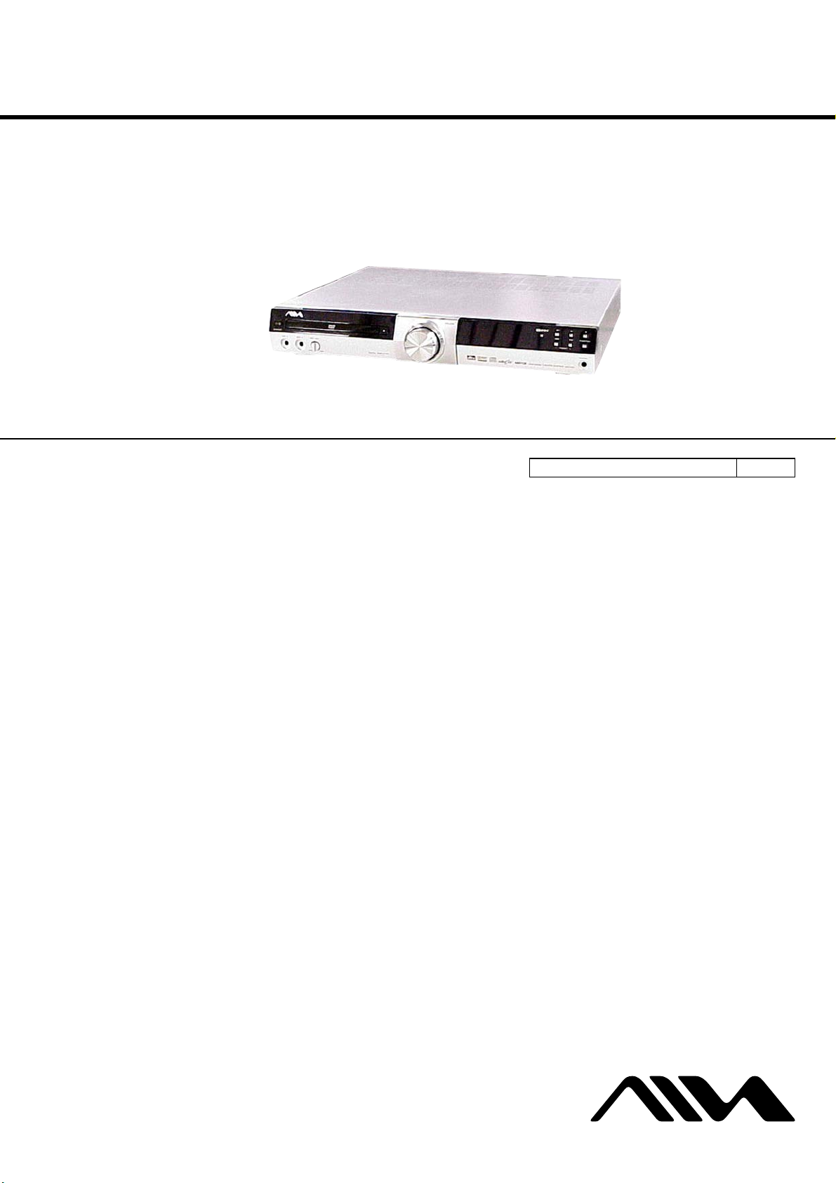
• CX-VX55/VX77 are DVD receiver
in AVJ-X55/X77.
Manufactured under license from Dolby Laboratories. “Dolby”, “Pro Logic”,
and the double-D symbol are trademarks of Dolby Laboratories.
Confidential Unpublished works. Copyright 1992–1997 Dolby
Laboratories. All rights reserved.
Manufactured under license from Digital Theater Systems, Inc. US Pat. No.
5,451,942 5,956,674, 5,974,380, 5,978,762 and other worldwide patents
issued and pending. “dts” and “DTS Digital Surround” are registered
trademarks of Digital Theatre Systems, Inc. Copyright 1996, 2000 Digital
Theater Systems, Inc. All rights reserved.
Photo: CX-VX55
AEP Model
UK Model
E Model
Australian Model
Model Name Using Similar Mechanism CX-VX33
General
Power supply 220 – 240 V AC, 50/60 Hz
Power consumption 100 W, No more than 1 W
(220 – 240 V AC)
(at the power saving mode)
Mass 4.9 kg
External dimensions 430 × 70 × 370.5 mm
(W × H × D)
Operating conditions
Temperature: 5 – 35°C
Operation status: Horizontal
Operating humidity 5 – 85%
CD/DVD
Laser Semiconductor laser,
wavelength 650 nm
for VCD and DVD,
wavelength 780 nm for CD
Emission duration Continuous
Signal system CX-VX55:
PAL 625/50, NTSC 525/60
(AEP, UK, CET, E3)
NTSC 525/60 (E41)
PAL, NTSC (AUS, SP, RU)
CX-VX77: PAL, NTSC
Frequency response 2 Hz – 20 kHz (±1.0 dB)
(audio)
Signal-to-noise ratio More than 75 dB
(audio) (1 kHz, NOP,
20 kHz LPF/A-Filter)
Dynamic range (audio) More than 70 dB
Harmonic distortion 0.5% (1 kHz, at 12 W position)
(audio) (20 kHz LPF/A-Filter)
SPECIFICATIONS
Video
Inputs
VIDEO (AUDIO IN): Sensitivity: 800 mV
Impedance: 50 kilohms
MIC (phone jacks): Sensitivity: 4 mV
Impedance: 10 kilohms
SCART (AUDIO IN): AEP, UK, CET, RU model:
Sensitivity: 800 mV
Impedance: 50 kilohms
Video output 1.0 V (p-p), 75 Ω,
negative sync., RCA jack
AEP, UK, CET, RU model:
EURO AV (TO TV)
S VIDEO OUT E3, E41, AUS, SP model:
(Y) 1.0 V (p-p), 75 ohms,
negative sync.,
Mini DIN 4-pin × 1
(C) 0.286 V (p-p), 75 ohms
COMPONENT VIDEO OUT
E3, E41, AUS, SP model:
(Y) 1.0 V (p-p), 75 ohms,
negative sync., RCA jack × 1
(PB/CB)/(PR/CR) 0.7 V (p-p),
75 ohms, RCA jack × 2
– Continued on next page –
DVD RECEIVER
9-879-239-04
2005J04-1
© 2005. 10
Sony Corporation
Personal Audio Division
Published by Sony Engineering Corporation
1
Page 2

CX-VX55/VX77
Tuner
FM
Tuning range 87.5 – 108 MHz
Intermediate frequency 10.7 MHz
Signal-to noise ratio 60 dB (Mono)
AM (MW)
Tuning range 522 – 1,611 kHz
Intermediate frequency 450 kHz
Amplifier
Stereo mode 80 W + 80 W
(6 Ω at 1 kHz, THD 10%)
Surround mode Front: 80 W + 80 W
(*Depending on the Centre*: 80 W
sound mode settings Surround*: 80 W + 80 W
and the source, there (6 Ω at 1 kHz, THD 10%)
may be no sound Subwoofer*: 150 W
output.) (3 Ω at 50 Hz, THD 10%)
Outputs PHONES: (32 Ω, 25 mW)
Design and specifications are subject to change without
notice.
• Abbreviation
CET : East European & Russian model
E3 : 240V AC area in E model
E41 : 230V AC area in E model
AUS : Australian model
SP : Singapore model
RU : Russian model
Notes on Chip Component Replacement
•Never reuse a disconnected chip component.
• Notice that the minus side of a tantalum capacitor may be
damaged by heat.
Flexible Circuit Board Repairing
•Keep the temperature of soldering iron around 270°C during
repairing.
• Do not touch the soldering iron on the same conductor of the
circuit board (within 3 times).
• Be careful not to apply force on the conductor when soldering
or unsoldering.
UNLEADED SOLDER
Boards requiring use of unleaded solder are printed with the lead
free mark (LF) indicating the solder contains no lead.
(Caution: Some printed circuit boards may not come printed with
the lead free mark due to their particular size)
: LEAD FREE MARK
Unleaded solder has the following characteristics.
• Unleaded solder melts at a temperature about 40 °C higher than
ordinary solder.
Ordinary soldering irons can be used but the iron tip has to be
applied to the solder joint for a slightly longer time.
Soldering irons using a temperature regulator should be set to
about 350 °C.
Caution: The printed pattern (copper foil) may peel away if the
heated tip is applied for too long, so be careful!
• Strong viscosity
Unleaded solder is more viscou-s (sticky, less prone to flow)
than ordinary solder so use caution not to let solder bridges occur such as on IC pins, etc.
• Usable with ordinary solder
It is best to use only unleaded solder but unleaded solder may
also be added to ordinary solder.
SAFETY-RELATED COMPONENT WARNING!!
COMPONENTS IDENTIFIED BY MARK 0 OR DOTTED LINE
WITH MARK 0 ON THE SCHEMATIC DIAGRAMS AND IN
THE PARTS LIST ARE CRITICAL TO SAFE OPERATION.
REPLACE THESE COMPONENTS WITH SONY P ARTS WHOSE
PART NUMBERS APPEAR AS SHOWN IN THIS MANUAL OR
IN SUPPLEMENTS PUBLISHED BY SONY.
2
Page 3
CX-VX55/VX77
Ver. 1.1
CAUTION
Use of controls or adjustments or performance of procedures
other than those specified herein may result in hazardous
radiation exposure.
NOTES ON HANDLING THE OPTICAL PICK-UP BLOCK
OR BASE UNIT
The laser diode in the optical pick-up block may suffer electrostatic
breakdown because of the potential difference generated by the
charged electrostatic load, etc. on clothing and the human body.
During repair, pay attention to electrostatic break-down and also
use the procedure in the printed matter which is included in the
repair parts.
The flexible board is easily damaged and should be handled with
care.
NOTES ON LASER DIODE EMISSION CHECK
The laser beam on this model is concentrated so as to be focused on
the disc reflective surface by the objective lens in the optical pickup block. Therefore, when checking the laser diode emission,
observe from more than 30 cm away from the objective lens.
Laser component in this product is capable
of emitting radiation exceeding the limit for
Class 1.
TABLE OF CONTENTS
1. GENERAL
Front Panel Controls................................................................ 4
Display Window Indicators ..................................................... 5
Remote Control ....................................................................... 6
Rear Panel Connections (AEP, UK, CET, RU Model) ............ 7
Rear Panel Connections (E3, E41, AUS, SP Model)............... 8
2. DISASSEMBLY
2-1. Top Cover ............................................................................ 9
2-2. Front Panel Assy ...............................................................10
2-3. DVD Mechanism Deck ..................................................... 10
2-4. Rear Panel Section ............................................................ 11
2-5. SMPS Board...................................................................... 11
2-6. DVD Board ....................................................................... 12
2-7. Main Board ....................................................................... 12
2-8. Base Unit ........................................................................... 13
3. ELECTRICAL TROUBLESHOOTING GUIDE
3-1. Audio Part.......................................................................... 14
3-2. DVD Part........................................................................... 18
3-3. Details and Waveforms on System Test and Debugging ... 25
4. TEST MODE .....................................................................38
5. ELECTRICAL ADJUSTMENT.................................... 39
This appliance is
classified as a CLASS 1
LASER product. The
label is located on the
left side of the unit as
viewed from the front.
6. DIAGRAMS
6-1. Block Diagram –DVD Section–........................................ 41
6-2. Block Diagram –Audio Section– ......................................42
6-3. Block Diagram –Tuner/Power Section–............................ 43
6-4. Printed Wiring Boards –DVD Section (1/2)–.................... 45
6-5. Printed Wiring Board –DVD Section (2/2)– ..................... 46
6-6. Schematic Diagram –DVD Section (1/3)–........................ 47
6-7. Schematic Diagram –DVD Section (2/3)–........................ 48
6-8. Schematic Diagram –DVD Section (3/3)–........................ 49
6-9. Printed Wiring Board –Main Section (1/2)– ..................... 50
6-10. Printed Wiring Board –Main Section (2/2)– ..................... 51
6-11. Schematic Diagram –Main Section (1/5)– ........................ 52
6-12. Schematic Diagram –Main Section (2/5)– ........................ 53
6-13. Schematic Diagram –Main Section (3/5)– ........................ 54
6-14. Schematic Diagram –Main Section (4/5)– ........................ 55
6-15. Schematic Diagram –Main Section (5/5)– ........................ 56
6-16. Printed Wiring Board –Display Section– .......................... 57
6-17. Schematic Diagram –Display Section–............................. 58
6-18. Printed Wiring Board –Key Section–................................ 59
6-19. Schematic Diagram –Key Section–................................... 60
6-20. Printed Wiring Board –Power Section– ............................61
6-21. Schematic Diagram –Power Section– ............................... 62
7. EXPLODED VIEWS
7-1. Front Panel Section ...........................................................67
7-2. Boards Section .................................................................. 68
7-3. DVD Mechanism Section.................................................. 69
8. ELECTRICAL PARTS LIST ........................................70
3
Page 4
CX-VX55/VX77
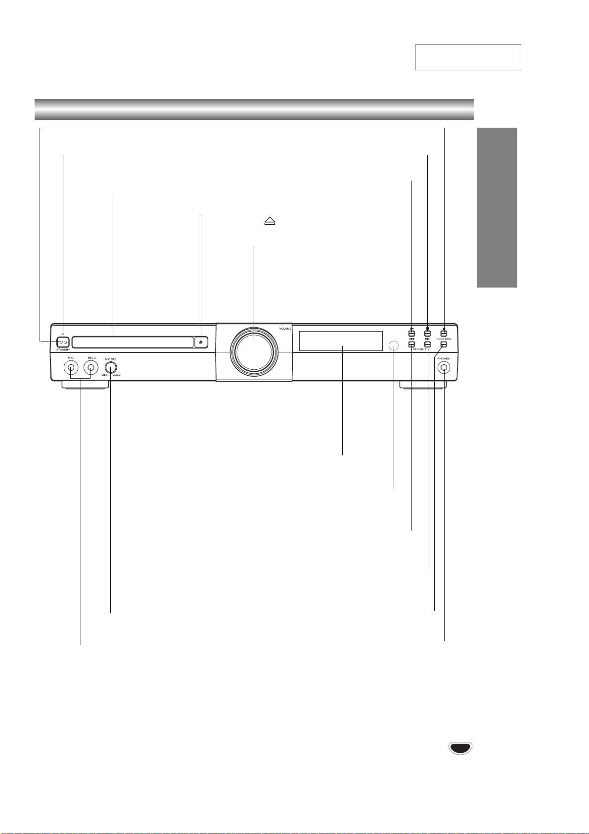
Front Panel Controls
SECTION 1
GENERAL
This section is extracted
from instruction manual.
@ / 1 (POWER) indicator
Switches the DVD Receiver ON and OFF.
STANDBY indicator
Lights red when the receiver
is in Standby mode (off).
Disc T ray
Insert a disc here.
Pause playback of a disc temporarily.
OPEN/CLOSE ( )
Opens or closes the disc tray.
VOLUME Control
Turn the knob clockwise to increase
sound level, counterclockwise to
decrease sound level.
Stops playback of a disc.
PLAY (
To play back a disc.
STOP (x)
PAUSE (X)
N)
INTRODUCTION
MIC VOL (MIN/MAX)
Adjust the microphone volume.
MIC1, MIC2
To connect microphone.
Display window
Point the DVD receiver remote control here.
DVD: Go to beginning of current chapter/track or to previous
RADIO:
To select preset station you want.
RADIO:
Remote Sensor
Reverse SKIP (.)
chapter/track.
Forward SKIP (
DVD: Go to NEXT chapter/track.
To select preset station you want.
FUNCTION
To select the Receiver’s source.
(FM, AM, VIDEO, TV or CD/DVD)
To connect headphones.
>
)
PHONES
7
4
Page 5
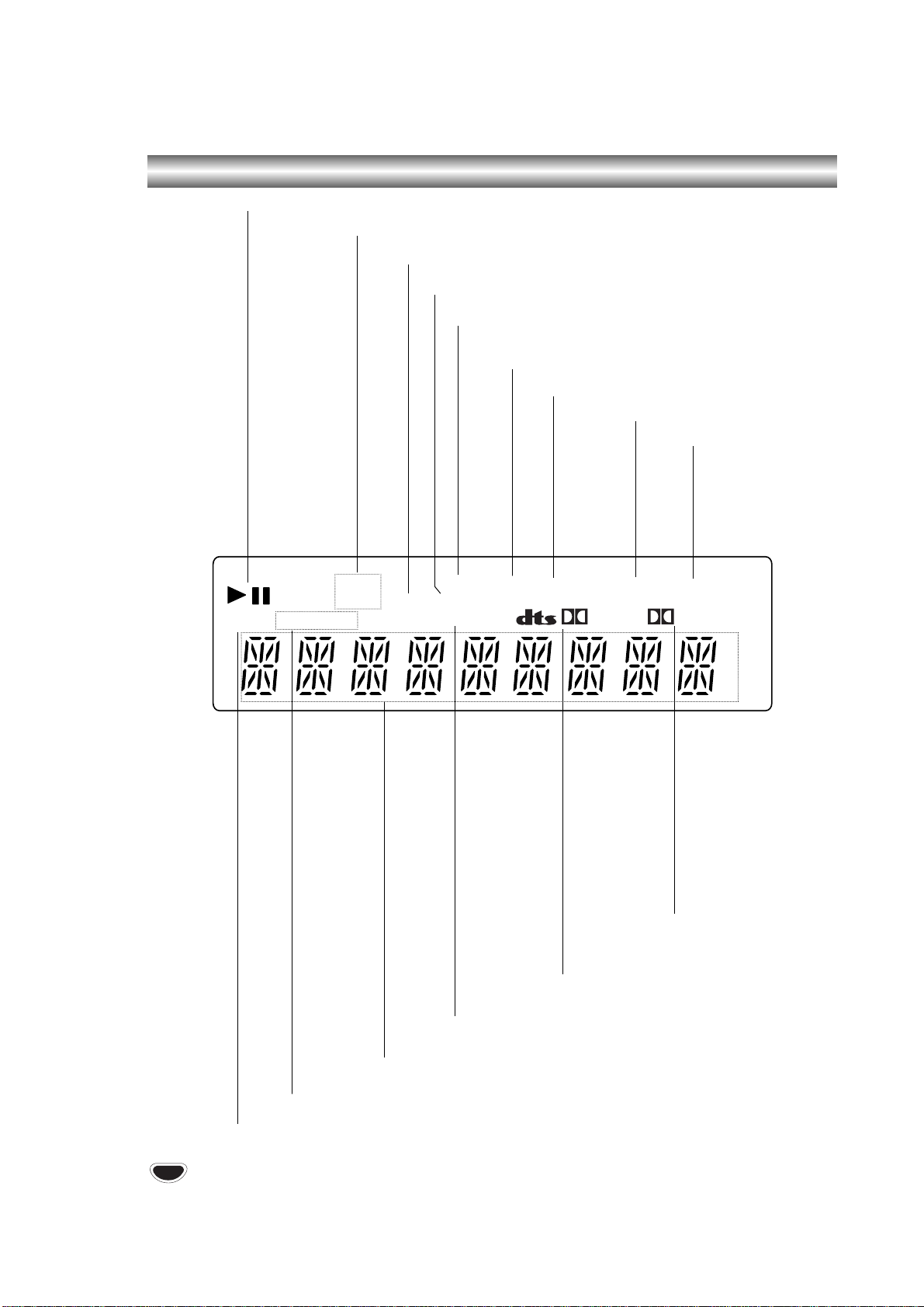
Display Window Indicators
Playing status.
Repeat playback mode indicators.
CX-VX55/VX77
Indicates the unit is radio mode.
Indicates the unit is stereo mode.
Lights up when the DVD Receiver
tunes in a station.
CD disc inserted.
MP3 disc inserted.
VCD2.0 disc inserted.
SLEEP timer indication
TITLE
DISC
REP 1 AM FM
CHAP
TRK
Total playing time/Elapsed time/Frequency/remaining time/ Current status/
Title number/Surround mode/Volume etc. indicators.
Indicates current chapter or
track number.
TUNED
CD
ST MONO
BASS
Lights up when the unit
is BASS ON mode.
MP3 PBC SLEEP
DIGITAL
Indicate current
surround format.
PRO LOGIC
Indicates sound format is
DOLBY PROLOGIC II.
II
Title indication
8
5
Page 6
CX-VX55/VX77
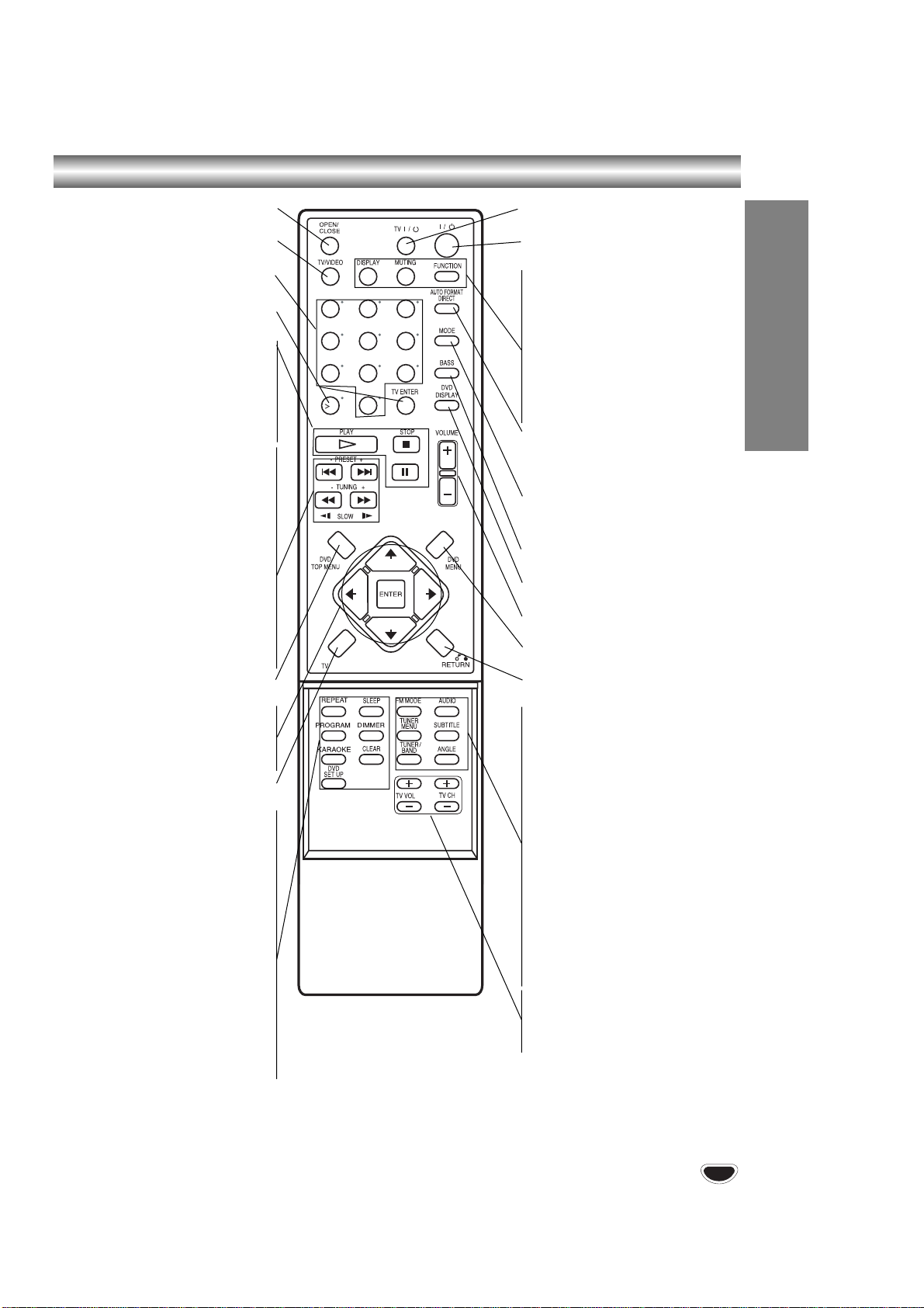
Remote Control
Opens and closes the disc tray.
TV/VIDEO
OPEN/CLOSE
Selects the TV’s source.
0-9 numerical buttons
Selects numbered options in a menu.
>10/ TV ENTER
Used to control TV.
Playback Control Buttons
H (PLAY)
Starts playback.
Pause playback or recording temporarily.
X (PAUSE)
x (STOP)
Stops playback.
PRESET-
Go to beginning of current chapter or
track or go to previous chapter or track.
Select programme of Tuner.
PRESET+
Go to next chapter or track.
Select programme of Tuner.
For picture search or slow playback
SLOW t/
To tune in the desired station.
SLOW T/
For picture search or slow playback
To tune in the desired station.
TUNING-
backward.
TUNING+
forward.
DVD T OP MENU
Displays the disc’s Title menu, if available.
B/b/V/v (left/right/up/down)
Selects an option in the menu.
ENTER
Acknowledges menu selection.
TV
To control TVs with the Remote.
REPEAT
Repeat chapter, track, title, all
SLEEP
To place the unit in the Sleep mode.
PROGRAM
Enters to the programme edit mode or
exits from that.
DIMMER
To change the brightness of the display
window.
KARAOKE
To display the Karaoke menu
audio channel.
CLEAR
Removes a track number on the program
menu.
DVD SETUP
Accesses or removes DVD setup menu.
12
45
89
7
-/--
10
10/0
PAUSE
TV @ / 1
Switches TV ON and OFF.
@ / 1
Switches DVD Receiver ON and OFF.
DISPLAY
To display remaining time between
3
6
Chapter and title.
To check the RDS service programme
(PS).
MUTING
Momentarily silence the speaker of the
DVD Receiver.
FUNCTION
To select the Receiver’s source.
(FM, AM, VIDEO, TV or CD/DVD)
INTRODUCTION
AUTO FORMAT DIRECT
Selects sound mode between A.F.D.
AUTO, PRO LOGIC, PLII MOVIE and
PLII MUSIC.
MODE
Selects sound mode between FLAT,
ROCK, POP, JAZZ, CLASSIC,NEWS
and LINK.
BASS
Switches BASS ON and OFF.
DVD DISPLAY
Accesses On-Screen display.
VOLUME (+/-)
Adjusts speaker volume.
DVD MENU
Accesses menu on a DVD disc.
RETURN
Returns the setup menu.
FM MODE
To change between MONO and
STEREO modes.
AUDIO
Selects an audio language (DVD) or an
audio channel (CD).
TUNER MENU
Memorize a radio station frequency
into the tuner.
Press to clear preset stations from the
tuner memory.
SUBTITLE
Selects a subtitle language.
TUNER/BAND
Selects the DVD Receiver’s tuner as the
listening choice. (FM and AM bands)
ANGLE
Selects a DVD camera angle if
available.
TV VOL +/–
Adjusts TV’s volume.
TV CH +/–
Selects TV’s channel.
9
6
Page 7

AEP, UK, CET, RU MODEL
Rear Panel Connections
AC Power Cord
Plug into the power source.
CX-VX55/VX77
EURO AV OUTPUT (TO TV)
Connect to your TV set.
MONITOR OUT (VIDEO)
Connect to a TV with video input.
VIDEO (AUDIO IN R/L)
Connect the audio output of an external
source (VCR, LD player, etc).
Connect the AM Loop antenna to this terminal.
SPEAKER CONNECTORS
Connect the six supplied speakers
to these terminals.
Do not touch the inner pins of the jacks on the rear
panel. Electrostatic discharge may cause permanent
damage to the unit.
Remote Control Operation Range
Point the remote control at the remote sensor and press
the buttons.
Distance: About 6m (20ft) from the front of the
remote sensor
Angle: About 30 in each direction of the front of the
remote sensor
AM LOOP ANTENNA CONNECTORS
FM ANTENNA CONNECTOR
Connect the FM antenna to this terminal.
Remote control battery installation
Detach the battery cover on the rear of
the remote control, and insert two R03
(size AAA) batteries with and
aligned correctly.
When using the remote control, point it
at the remote sensor on the unit.
10
Do not mix old and new batteries.
7
Page 8
CX-VX55/VX77
E3, E41, AUS, SP MODEL
Rear Panel Connections
AC Power Cord
Plug into the power source.
SPEAKER CONNECTORS
Connect the six supplied
speakers to these terminals.
MONITOR OUT (VIDEO)
Connect to a TV with video input.
VIDEO (AUDIO IN L/R)
Connect the audio output of an external
source (VCR, LD player, etc).
MONITOR S VIDEO OUT (DVD OUT)
Connect to a S Video Input on TV.
FOR DVD VIEWING ONLY.
COMPONENT VIDEO OUT (Y P
Connect to a TV with Y P
FOR DVD VIEWING ONLY.
Connect the AM Loop antenna to this terminal.
Do not touch the inner pins of the jacks on the rear
panel. Electrostatic discharge may cause permanent
damage to the unit.
Remote Control Operation Range
Point the remote control at the remote sensor and press
the buttons.
Distance: About 6m (20ft) from the front of the
remote sensor
Angle: About 30 in each direction of the front of the
remote sensor
B/CB PR/CR)
B/CB PR/CR inputs.
AM LOOP ANTENNA CONNECTORS
FM ANTENNA CONNECTORS
Connect the FM antenna to this terminal.
Remote control battery installation
Detach the battery cover on the rear of
the remote control, and insert two R03
(size AAA) batteries with and
aligned correctly.
When using the remote control, point it
at the remote sensor on the unit.
Do not mix old and new batteries.
10
8
Page 9
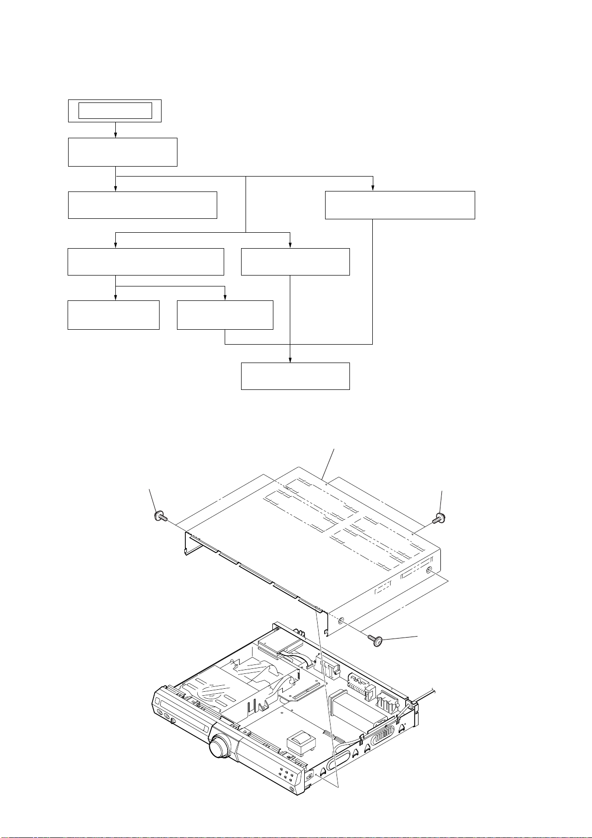
SECTION 2
s
DISASSEMBLY
Note : This set can be disassemble according to the following sequence.
SET
2-1. TOP COVER
(Page 9)
CX-VX55/VX77
Ver. 1.1
2-2. FRONT PANEL ASSY
(Page 10)
2-3. DVD MECHANISM DECK
(Page 10)
2-8. BASE UNIT
2-6. DVD BOARD
(Page 13)
(Page 12)
2-5. SMPS BOARD
(Page 11)
2-7. MAIN BOARD
(Page 12)
Note : Follow the disassembly procedure in the numerical order given.
2-1. TOP COVER
2
two
screws
2-4. REAR PANEL SECTION
(Page 11)
4
top cover
3
two
screw
1
two
screws
9
Page 10
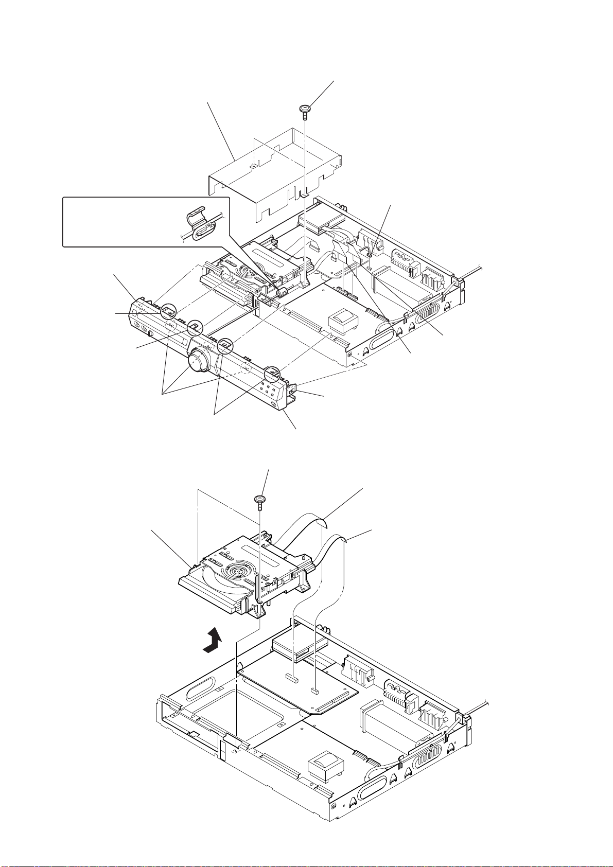
CX-VX55/VX77
)
Ver. 1.1
2-2. FRONT PANEL ASSY
6
Remove the ferrite core
attached to the power cord.
8
claw
qa
claw
7
claw
2
shield (barrier)
1
two
screws
3
PN202 (5P)
5
4
PN101 (23 core
PN102 (24 core)
qs
three claws
2-3. DVD MECHANISM DECK
5
DVD mechanism deck
0
two claws
4
3
two
qd
screws
9
claw
front panel assy
PDM01 (23 core)
1
2
PDM02 (11 core)
10
Page 11
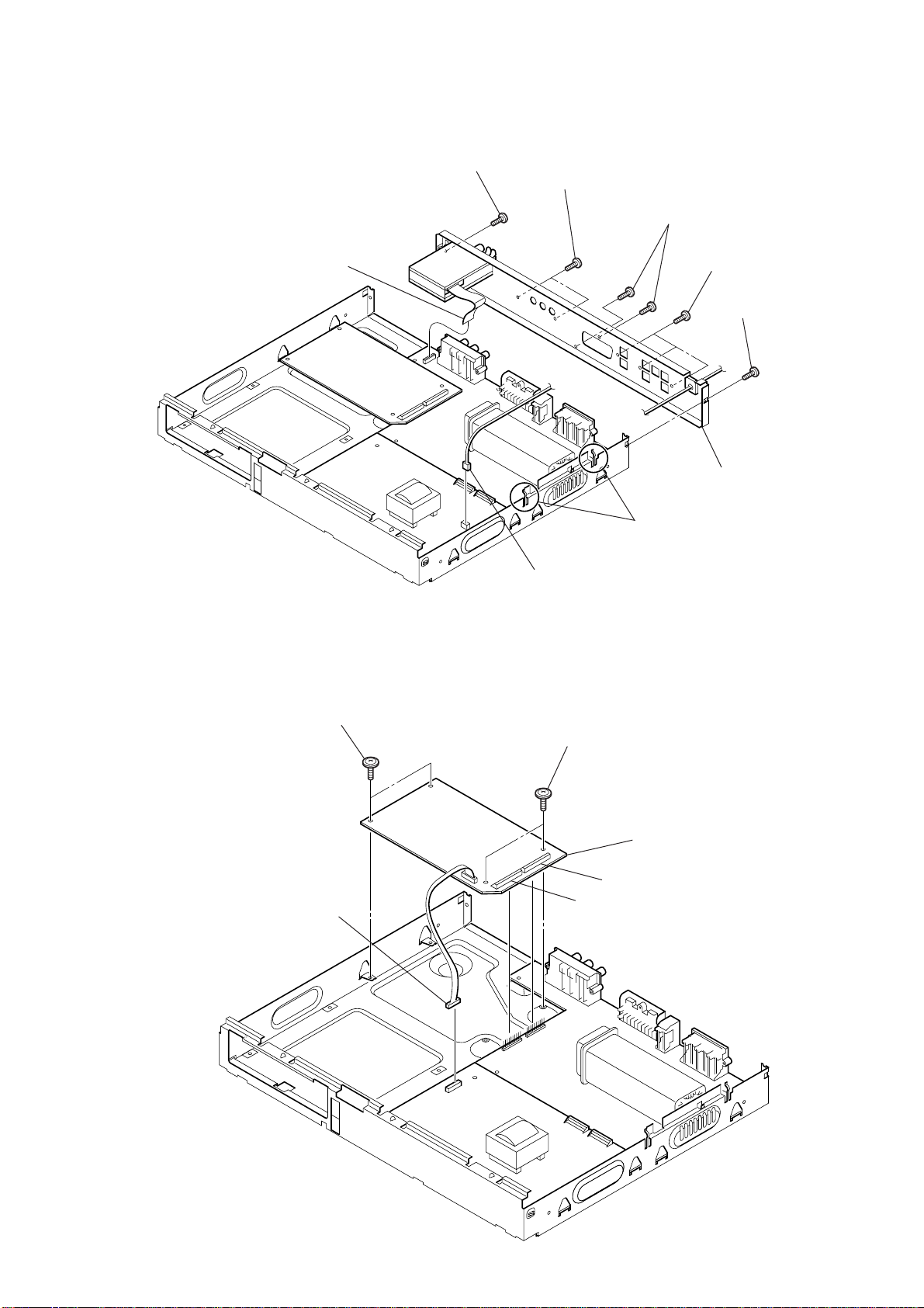
2-4. REAR PANEL SECTION
3
PN103 (12 core)
4
screw
5
two
screws
6
two
CX-VX55/VX77
screws
7
three
screws
8
screw
9
rear panel section
Ver. 1.1
2-5. SMPS BOARD
1
CN903 (10P)
3
two
screws
2
PN901 (2P)
2
two
screws
PDA02
PDA03
1
Pull up the two claws
pressing the power cord.
4
DVD board
11
Page 12
CX-VX55/VX77
s
Ver. 1.1
2-6. DVD BOARD
2
two
screws
CN902
1
two
CN901
3
SMPS board
screws
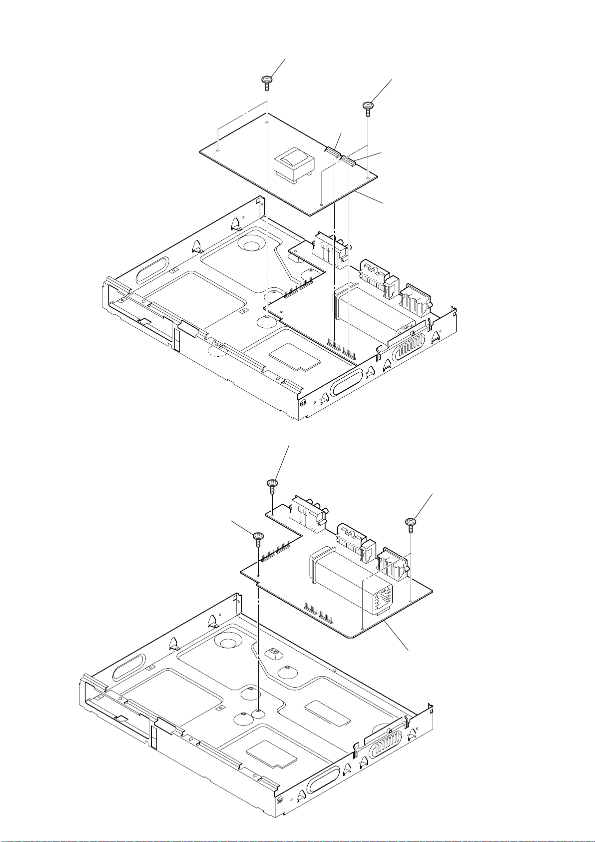
2-7. MAIN BOARD
3
screw
(+BVTP 3
×
10)
2
screw
4
1
two
MAIN board
screw
12
Page 13
2-8. BASE UNIT
s
7
two drawing
9
2
holder assy
screws
two
rubbers
1
two drawing
screws
8
two
rubbers
0
6
two drawing
base unit
CX-VX55/VX77
Ver. 1.1
screw
5
tray assy
4
3
guide
13
Page 14
CX-VX55/VX77
Ver. 1.1
3-1. AUDIO PART
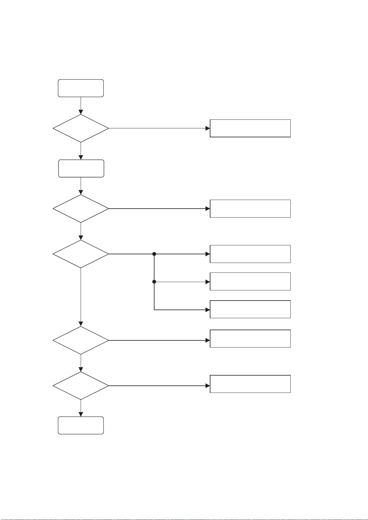
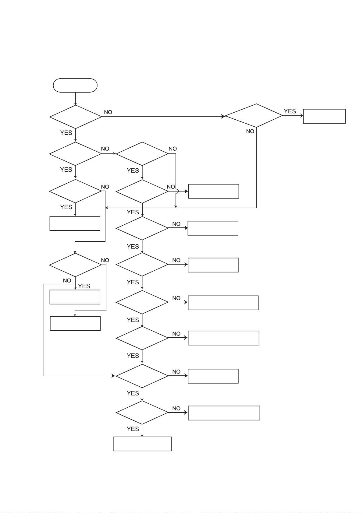
1. Power check flow
POWER CORD.
SECTION 3
ELECTRICAL TROUBLESHOOTING GUIDE
INSERT
TURN ON
THE RED LED?
YES
TURN POWER ON.
IS POWER ON?
YES
DOES INITIAL
READ WORK?
YES
NO
NO
NO
CHECK POWER PLUG
AND POWER SUPPLY CIRCUIT.
CHECK POWER SUPPLY CIRCUIT.
CHECK LASER CIRCUIT.
CHECK FOCUS CIRCUIT.
DOES IT PLAY?
YES
DOES IT OUTPUT
AUDIO?
YES
OK
NO
NO
CHECK DISC.
CHECK TRACKING SERVO CIRCUIT.
CHECK AUDIO CIRCUIT.
14
Page 15
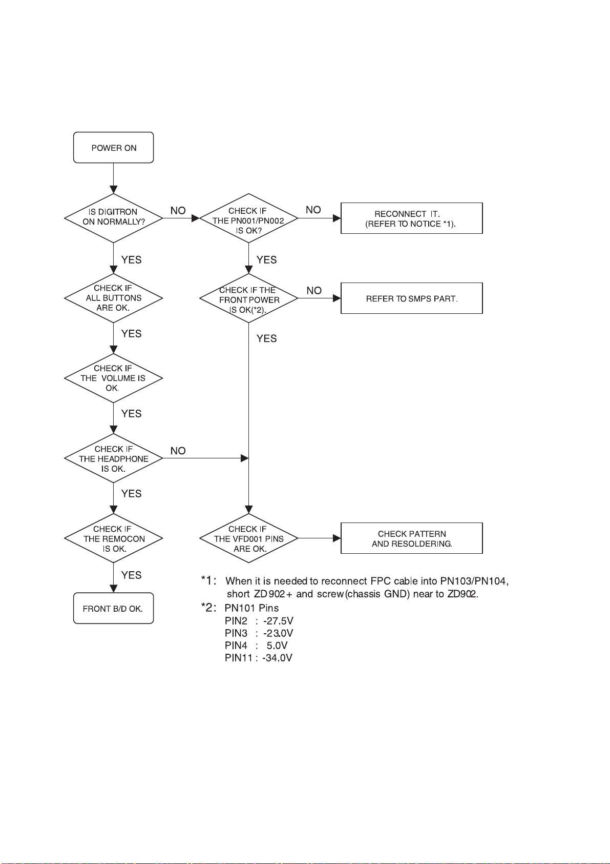
POWER ON
Does it appear
DVD Error at
Does other function
name appear at FLD?
FLD?
Check
Connector(PN902)if
is normally.
Check power part
of Main B/D.
Check oscillator
of X101.
Check if IC101
PIN1 is High.
Check if IC101
PIN11 is High.
Check if IC101 PIN
17, 46, 72, 90 is high
(5V).
Check if IC101
PIN26 is High.
Replace IC101.
Does CD/DVD
appear at FLD?
Reconnect it.
Refer to SMPS.
OK.
Refer to oscillator
Circuit.
Check DVD Reset Waveform.
Check IC101 Reset Waveform.
Check 5V line.
Check Power dection Circuit.
Does LOADING
appear at FLD?
Does no Disc or
Time appear at FLD?
Check if DVD an Audio
Micom Interface is OK.
Check power.
Check DVD Module.
Check SMPS.
CX-VX55/VX77
Ver. 1.1
2. AUDIO µ.COM CIRCUIT
15
Page 16
CX-VX55/VX77
Ver. 1.1
3. FRONT CIRCUIT (1/2)
16
Page 17
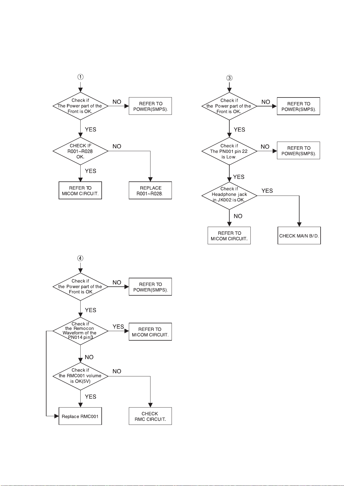
4. FRONT CIRCUIT (2/2)
CX-VX55/VX77
Ver. 1.1
17
Page 18
CX-VX55/VX77
Ver. 1.1
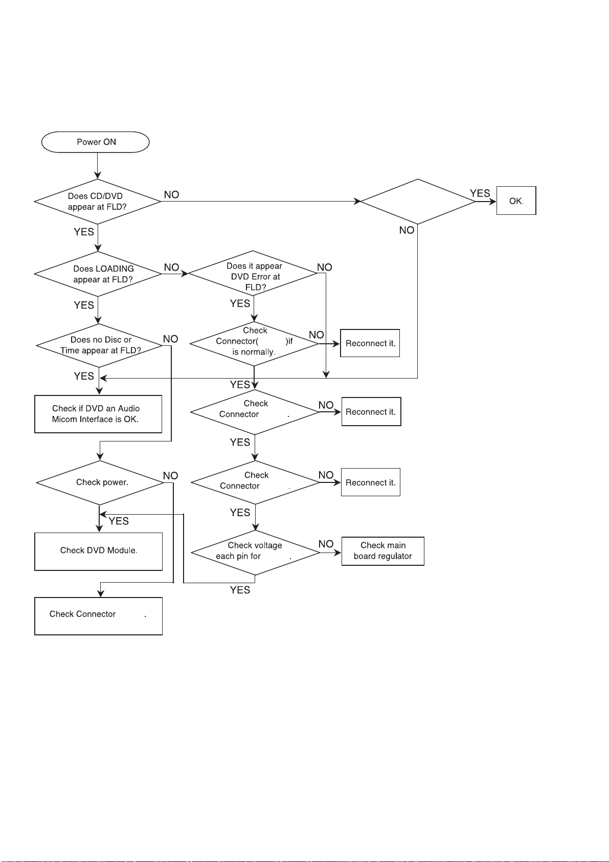
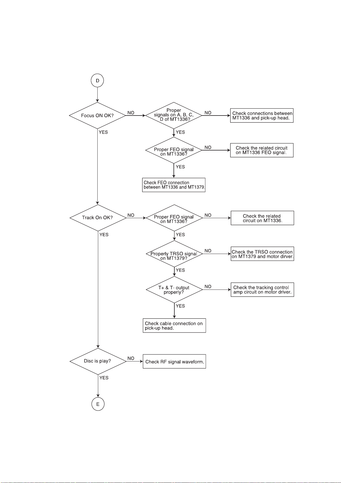
3-2. DVD PART
1. Power check flow
Does other function
name appear at FLD?
PDA01
PDM02
PDM01
PDA02
PDA03
18
Page 19
2. Test & debug flow
CX-VX55/VX77
Ver. 1.1
19
Page 20
CX-VX55/VX77
Ver. 1.1
20
Page 21
CX-VX55/VX77
Ver. 1.1
21
Page 22
CX-VX55/VX77
Ver. 1.1
22
Page 23
CX-VX55/VX77
Ver. 1.1
23
Page 24

CX-VX55/VX77
Ver. 1.1
24
Page 25

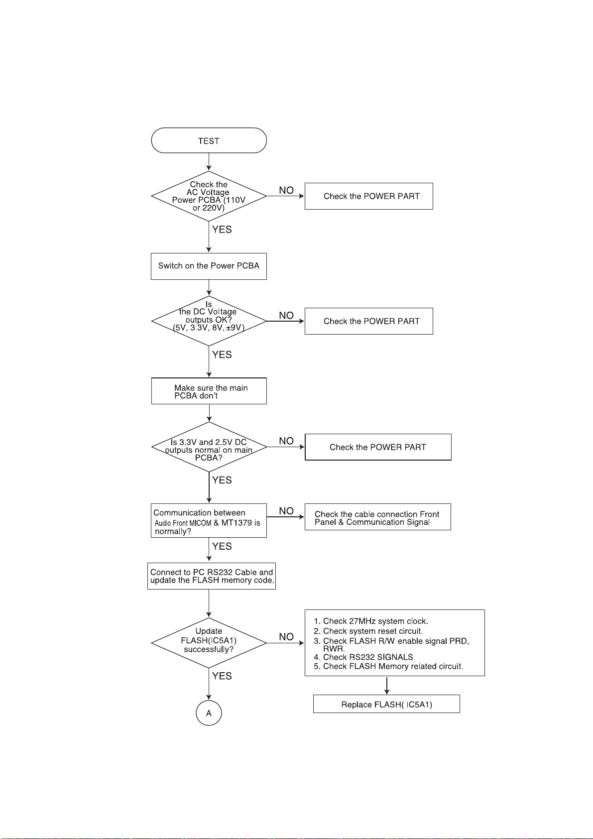
3-3. DETAILS AND WAVEFORMS ON SYSTEM TEST AND DEBUGGING
1. SYSTEM 27MHz CLOCK, RESET, FLASH R/W SIGNAL
1) MT1379 main clock is at 27MHz (X501)
CX-VX55/VX77
Ver. 1.1
2) MT1336 reset is high active
25
Page 26

CX-VX55/VX77
Ver. 1.1
3) RS232 waveform during procedure (Downloading)
4) Flash R/W enable signal during download (Downloading)
26
Page 27

2. SDRAM CLOCK
1) MT1379 main clock is at 27MHz (X501)
CX-VX55/VX77
Ver. 1.1
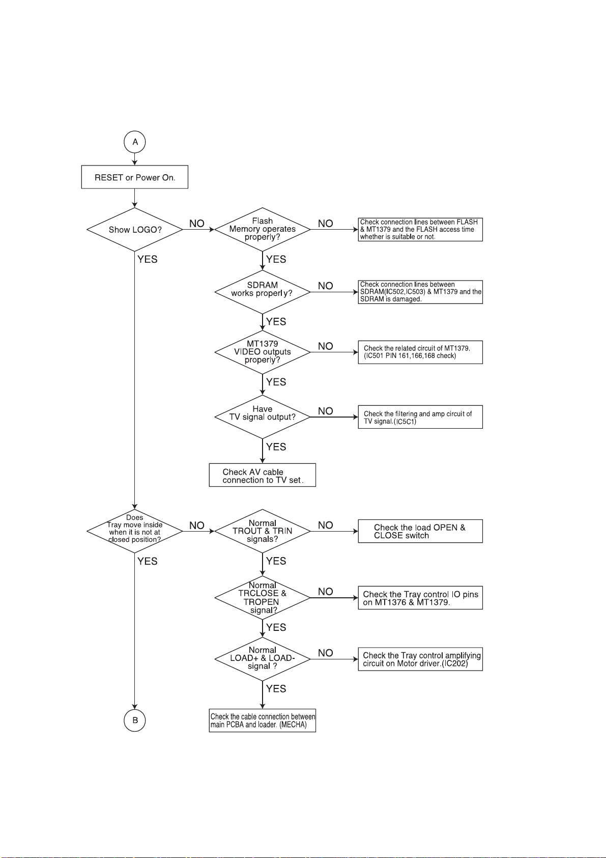
3. TRAY OPEN/CLOSE SIGNAL
1) Tray open/close waveform
27
Page 28

CX-VX55/VX77
Ver. 1.1
2) Tray close waveform
3) Tray open waveform
28
Page 29

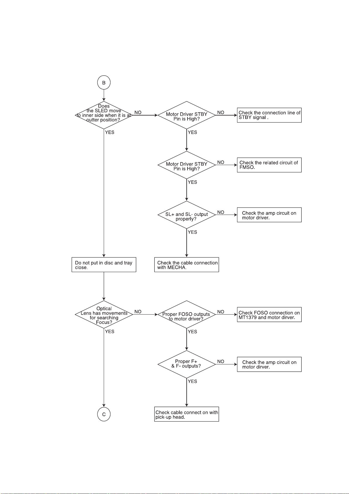
4. SLED CONTROL RELATED SIGNAL (NO DISC CONDITION)
CX-VX55/VX77
Ver. 1.1
5. LENS CONTROL RELATED SIGNAL (NO DISC CONDITION)
29
Page 30

CX-VX55/VX77
Ver. 1.1
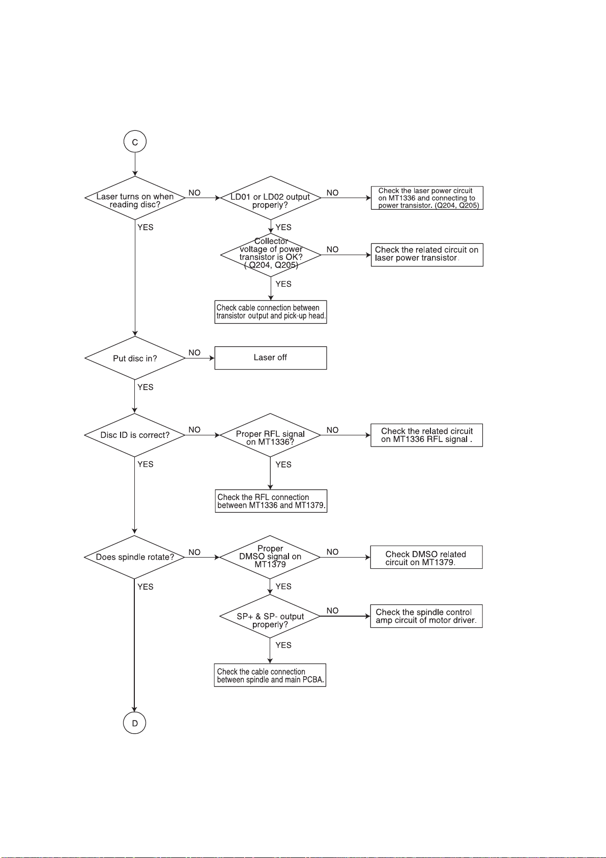
6. LASER POWER CONTROL RELATED SIGNAL (NO DISC CONDITION)
7. DISC TYPE JUDGEMENT WAVEFORM
30
Page 31

CX-VX55/VX77
Ver. 1.1
31
Page 32

CX-VX55/VX77
Ver. 1.1
8. FOCUS ON WAVEFORM
32
Page 33

CX-VX55/VX77
Ver. 1.1
9. SPINDLE CONTROL WAVEFORM (NO DISC CONDITION)
33
Page 34

CX-VX55/VX77
Ver. 1.1
10. TRACKING CONTROL RELATED SIGNAL (SYSTEM CHECKING)
34
Page 35

11. RF WAVEFORM
CX-VX55/VX77
Ver. 1.1
12. MT1379 AUDIO OPTICAL AND COAXIAL OUTPUT (ASPDIF)
35
Page 36

CX-VX55/VX77
Ver. 1.1
13. MT1379 VIDEO OUTPUT WAVEFORM
1) Full colorbar signal (CVBS)
2) Y
36
Page 37

3) C
CX-VX55/VX77
Ver. 1.1
14. AUDIO OUTPUT FORM AUDIO DAC
1) Audio related Signal
37
Page 38

CX-VX55/VX77
Ver. 1.1
SECTION 4
TEST MODE
DVD Processor Reset Procedure:
1. Press the DVD SETUP key on the remote commander to
enter the set up screen. The following SET UP menu is displayed.
2. Move the cursor to [TV Aspect,16:9 Wide] on the screen.
3. Press the following keys in the order of 1 t 3 t 9 t 7
t 1 t 3 t 9 t ENTER on the remote commander.
4. The following menu is displayed and the DVD Processor is
reset to the default set up when the product is shipped from
the factory.
5. Press any key on the remote commander to exit this mode.
The DVD Processor reset procedure is completed.
38
Page 39

SECTION 5
ELECTRICAL ADJUSTMENT
[RFMON Level Check]
Connection:
oscilloscope
DVD board
PDM01 pin 2(RFOUT)
6
PDM01 pin
(GND PD)
Procedure:
1. Connect an oscilloscope to PDM01 pin 2 (RFOUT) and
PDM01 pin 6 (GND PD) on the DVD board.
2. Turn the power on.
3. Set the test disc (DVD: TDV-520CSO, CD: LUV-P01) on the
tray and touch the B button to playback.
4. Confirm that oscilloscope waveform is clear and check RFOUT
signal level is correct or not.
Note: A clear RFOUT signal waveform means that the shape “◊” can be
clearly distinguished at the center of the waveform.
RFOUT signal waveform
+
–
VOLT/DIV: 200 mV
TIME/DIV: 500 ns
CX-VX55/VX77
Ver. 1.1
level:
1.09 ± 0.2 Vp-p (DVD)
1.05 ± 0.2 Vp-p (CD)
Checking Location: DVD board (COMPONENT SIDE)
[DVD BOARD](COMPONENT SIDE)
2
10
1
11
PDM01 pin 2(RFOUT)
IC202
2
1
PDM01
PDM01 pin
22
23
6
(GND PD)
IC505
IC201
IC5C1
IC5A1
IC501
IC506
39
Page 40

CX-VX55/VX77
Ver. 1.1
MEMO
40
Page 41

6-1. BLOCK DIAGRAM — DVD SECTION —
SECTION 6
DIAGRAMS
CX-VX55/VX77
Ver. 1.1
OPTICAL
PICK-UP
BLOCK
TRACKING+
TRACKING–
SLED
MOTOR
LOADING
MOTOR
SPINDLE
MOTOR
RF OUT
VCC
LD DVD
LD CD
MD CD
VREF
VR VDD
VR CD
SW PDIC
FOCUS +
FOCUS –
A
B
C
D
E
F
M702
M703
M701
AVCC+5V
Q204
LD
DRIVE
Q203
MOTOR/COIL DRIVER
VO4+
6
VO4–
7
VO3–
9
VO3+
8
VO1–
13
VO1+
12
VLO+
5
VLO–
4
VO2–
11
VO2+
10
Q205
LD
DRIVE
Q202
IC202
Q201
MUTE
REV
FWD
VIN4–
VIN3–
VIN1
VIN-8
VIN2-
IC201
CD/DVD RF AMP,
SERVO CONTROL
DVDRFIP
96
104
MD
101
MA
102
MB
103
MC
DVDC
98
DVDB
99
100
DVDA
DVDD
97
TNI
116
TPI
115
126
LD02
LD01
125
MDI2
124
MDI1
123
17
V2O
IO8
50
IOB
53
REFCOS
72
71
HALLCOS
COSPHI
70
IOA
52
V2REFO
15
16
34
2
1
32
24
15
WE
CAS
RASCSCKE
18
21
16
17 18 19 37 38 20
CLK
RFOP
RFON
FEO
LVL
CSO
TEO
DEFECT
HTRC
HRFRP
SCLK
SDEN
SDATA
RST
DPDMUTE
IO5
IO6
IO7
VREFO
IC506
BA0
BA1
21 15 39
18
19
20
21
23
30
25
56
58
59
60
61
47
48
49
SDRAM
DQML
DQM0
DQM1
6
7
DQMH
TR IN
TR OUT
LIMIT
A0-10
22-26
29-35
MA0-11
(CLOSE)
(OPEN)
10,11,13,42
44,45,47,48
DQ
0-15
DQ0-15
2,4,5,7,8
50,51,53
SW2 (OPEN/CLOSE)
SW1 (LIMIT)
DQ0-15
78-81,83-85,
93-96,98-101
MA0-11
105-107,110,119
112-114,121-124
X501
27MHz
216
215
205
206
204
203
198
209
207
208
197
196
195
188
16
210
211
200
14
13
19
18
12
SP DATA
116,117
118
91
103
104
90
89
88
87
186
187
RFIP
RFIN
FEI
RFLEVEL
CSO
TEI
BDO
HRFZC
RFRPDC
RFRPAC
SCLK
SDEN
SDATA
PRST
PWMOUT2
PWMVREF
PWM2VREF
ADIN
TR OPEN PWR
TRO
FMO
DMO
FOO
BA1
BA0
CLK
CLE
RCS#
RAS#
CAS#
RWE#
XTALO
XTALI
IC501
MPEG & VIDEO PROCESS
HIGH0-7
IOA0-7
IOA18-20
A16,17
RD
0-15
RA
0-11
DQM0,1
YUV6/R
173
YUV5/B
172
170
YUV4/G
YUV2/Y
166
YUV1/C
164
UP3-1
69
UP1-5
64
UP1-2
61
68
UP3-0
YUV7
177
UP3-5
74
UP3-4
73
31-34
AD0-7
36-39
22-27
29,30,40,41
43-53
IOWR#
58 11
IOOE#
57
59
IOCS#
SP DATA
181
MC DATA
152
ACLK
151
ABCK
148
149
ALRCK
ASDATA0
154
155
ASDATA1
ASDATA2
156
ASDATA3
157
UP1-7
67
UP1-6
65
AD0-7
A0-20
5
6
DVD VIDEO
14
12
10
6
2
IC505
EEPROM
SDA
SCL
IC5C1
DRIVE
CR
CB
CY
CVB
Y
C
100
29,31,33
35,38,40
42,44
1-9,16-25
45,48
98
99
3
28
26
16
18
20
23
21
26
DVD SO
DVD SI
DVD CK
DVD CS
WE
OE
CE
Q501
R/G/B VIDEO
TV MODE
DVD RESET
IC101
(1/3)
SYSTEM CONTROL
IC5A1
FLASH MEMORY
I/O
0-7
A-1
A0-18
NC
A SPDATA
MIC DATA
ACLK
ABCK
ALRCK
ADATA0
ADATA1
ADATA2
ADATA3
16:9/4:3
RESET
Q606
Q607
79
78
77
1
12
A
AUDIO
SECTION
(Page 42)
JK601 (1/2)
PR(R)
PB(B)
Y(G)
MONITOR OUT
Y
C
JK602 (1/2)
G
B
R
AEP,UK,CET,RU MODEL
J6
TXD
RXD
Q602
RGB
SELECT
Q601,603-605
SCART
CONTROL
MONITOR OUT
R/G/B SELECT
SCART CONTROL
DV+3.3V
• R-ch is omitted due to same as L-ch.
• Signal Path
: AUDIO
: CD PLAY
: DVD PLAY
:Y
: CHROMA
: COMPONENT VIDEO
• Abbreviation
E3 : 240V AC area in E model
E41 : 230V AC area in E model
AUS : Australian model
SP : Singapore model
CET : East European & Russian model
RU : Russian model
E3,E41,AUS,SP MODEL
PR/CR
PB/CB
Y
VIDEO
(DVD ONLY)
OUTPUT(TO TV)
COMPONENT
S VIDEO
EURO AV
VIDEO OUT
MONITOR
OUT
CX-VX55/VX77
41 41
Page 42

CX-VX55/VX77
Ver. 1.1
6-2. BLOCK DIAGRAM — AUDIO SECTION —
DVD
SECTION
(Page 41)
JK002
MIC 1
JK003
MIC 2
TUNER/POWER
SECTION
(Page 43)
JK601 (2/2)
VIDEO
AUDIO IN
JK602
EURO AV
OUTPUT(TO TV)
AEP,UK,CET,RU MODEL
A
B
L
R
JK602 (2/2)
ADATA0
ADATA1
ADATA2
ADATA3
ALRCK
ABCK
ACLK
ASPDATA
MIC DATA
TU-L
R-CH
AUDIO IN L
R-CH
IC001
MIC DUAL PRE AMP
8
2
7
3
IC202
A/D CONVERTER
4
MCLK
LRCK
3
2
SCLK
1
SDATA
IC204
A/D CONVERTER
MCLK
4
LRCK
3
SCLK
2
1
SDATA
AIN R
AIN L
AIN R
AIN L
VR002
MIC VOL
4CH AUDIO SWITCH
1
2
5
5
8
5
8
IC002
MIC AMP
26
IC601
9 10
MIC DET
222368
4052B
R-CH
4052A
3
IC501
AUDIO AMP
21
X201
9.8304MHz
IC101
(2/3)
SYSTEM CONTROL
IC301
DIGITAL AUDIO PROCESSOR
PWMHPL+
PWMHPL–
PWMHPR+
PWMHPR–
23
SSDIN0
SSDIN1
24
25
SSDIN2
26
SSDIN3
20
SLRCK
19
SBCK
86
CLK IN
SO/SDA
SCK/SCL
RESET
PLL_XPD
79 80 92 4
9818 SDA
OVERLOAD
76
73
268891 74 7025
9818 CLK
PWR SNS
9818 PDN
9818 RESET
PWM6+
PWM6–
PWM1+
PWM1–
PWM5+
PWM5–
PWM2+
PWM2–
PWM4+
PWM4–
PWM3+
PWM3–
D301
46
45
41
40
FRONT L+
68
FRONT L–
67
FRONT R+
49
FRONT R–
48
67
68
REAR R+
52
REAR R–
51
CENTER+
59
CENTER–
58
S/WOOFER+
55
S/WOOFER–
54
P.SENS
R-CH
R-CH
R-CH
R-CH
R-CH
R-CH
D
X101
9.8304MHz
16 15
CF2
TUNER/POWER
SECTION
(Page 43)
CF1
IC502
HEADPHONE AMP
3
2
24 85
71
HP DET
HP MUTE
501/505 FAULT
501/505 TH WARN
1
505PDN
IC710
AUDIO POWER DRIVE
30
FRONT L+
29
FRONT L–
TH_WAR
28
FAULT
27
26
TRI_STATE
PWRDN
25
32
SURROUND L+
31
SURROUND L–
IC750
AUDIO POWER DRIVE
32
CENTER+
CENTER–
31
TH_WAR
28
FAULT
27
TRI_STATE
26
25
PWRDN
30
S/WOOFER +
S/WOOFER –
29
IC770
AUDIO POWER DRIVE
WOOFER+
30,32
WOOFER–
29,31
28
TH_WAR
27
FAULT
26
TRI_STATE
25
PWRDN
Q503
MUTE
Q609,983
MUTE
CONTROL
10,11
16,17
R-CH
R-CH
2,3
8,9
2,3
8,9
10,11
16,17
2,3
8,9
10,11
16,17
D801
R-CH
R-CH
D802
+12V
• R-ch is omitted due to same as L-ch.
• Signal Path
: AUDIO
• Abbreviation
CET : East European & Russian model
RU : Russian model
R-CH
FRONT L+
FRONT L–
FRONT R+
FRONT R–
SURROUND L+
SURROUND L–
SURROUND R+
SURROUND R–
CENTER+
CENTER–
WOOFER+
WOOFER–
FAN MOTOR
CONTROL
Q701
MUTE
FAN MOTOR
DRIVE
Q702
JK700
JK001
PHONES
TUNER/POWER
C
SECTION
(Page 43)
FRONT L (6Ω)
FRONT R (6Ω)
SURR L (6Ω)
SURR R (6Ω)
CENTER (6Ω)
JK701
SUBWOOFER
(3Ω)
FAN901
CX-VX55/VX77
4242
Page 43

6-3. BLOCK DIAGRAM — TUNER/POWER SECTION —
CX-VX55/VX77
Ver. 1.1
PN103
T AUDIO L OUT
T AUDIO R OUT
TM301
TUNER
PACK
FOR
DOWNLOAD
PN105
STEREO
T DI
TDO
T CLK
T CE
T RDS DATA
T RDS CLK
DATA0
DATA1
CLK
RESET
LED001
STANDBY
• R-ch is omitted due to same as L-ch.
• Signal Path
: AUDIO (TUNER)
R-CH
5.6VCPU
VFD001
DIGITRON
F1 F2
RMC001
REMOTE
CONTROL
RECEIVER
VR001
VOLUME
TUL
Q101
RESET
Q001
LED ON/OFF
SWITCH
SW001-008
FUNCTION
KEY
B
(Page 42)
AUDIO
SECTION
5V
IC101 (3/3)
SYSTEM CONTROL,FL DRIVER
4
STEREO
9
T DI
8
TDO
7
T CLK
5
T CE
6
T RDS DATA
10
T RDS CLK
96
DATA0
95
DATA1
97
CLK
11
RESET
41-45
47-50
P1-17
52-59
30-40
G1-11
27
STANDBY LED
291
REMOCON
18
KEY1
20
VOL UP
21
VOL DN
P CTL
AUDIO
SECTION
(Page 42)
AUDIO
SECTION
(Page 42)
5.6VCPU
5V
IC924
+8V
+12VA
2
+8V REG
+3.3V
+2.5V
D924
D929
-12VF
VKK(-28.5V)
D928
F1
F2
+35VF
C
D
IC921
+5V REG
2
IC922
+12V REG
2
IC923
+3.3V REG
2
Q921,922
-12V REG
Q971,975
-28V REG
POWER
CONTROL
Q973,982
POWER
CONTROL
MUTE
P.SENS
4
4
4
Q972
REG
1
11 2
1
IC942
IC941
REG
PC912
VOLTAGE
DETECT
D921
D922
D923
D924
D926
D927
D941
D951
T901
PC910
VOLTAGE
DETECT
T902
D903
D902
D911,912
ZD911
+5V REG
VOLTAGE
DETECT
BD901
IC901
POWER PROTECTION
DRAIN
6
7
DRAIN
8
DRAIN
2
VCC
VFB
3
Q910
PC911
IC902
POWER PROTECTION
D
1
4
VCC
7
OCP/BD
FB
6
AC IN
CX-VX55/VX77
43 43
Page 44

CX-VX55/VX77
d
Ver. 1.1
• Circuit Boards Location
MOTOR board
JACK (AUDIO) board
KEY board
DISPLAY board
THIS NOTE IS COMMON FOR PRINTED WIRING
BOARDS AND SCHEMATIC DIAGRAMS.
(In addition to this, the necessary note is
printed in each block.)
DVD board
SMPS board
MAIN boar
• Waveforms
1
IC201 qk (FEO)
100mV/DIV, 1ms/DIV
2
IC201 wa (TEO)
500mV/DIV, 1ms/DIV
3
IC201 oh (DVDRFIP)
0.2Vp-p
0.3Vp-p
— MAIN Board —— DVD Board —
1
IC101 qh (CF2)
1V/DIV, 10ns/DIV
2
IC301 ih (CLK IN)
1V/DIV, 10ns/DIV
1.6Vp-p
9.8304MHz
1.8Vp-p
12.288MHz
for schematic diagram:
• All capacitors are in µF unless otherwise noted. (p: pF)
50 WV or less are not indicated except for electrolytics
and tantalums.
• All resistors are in Ω and 1/
specified.
f
•
• 2 : nonflammable resistor.
• C : panel designation.
Note: The components identified by mark 0 or dotted line
• A : B+ Line.
• B : B– Line.
• H : adjustment for repair.
•Voltage and waveforms are dc with respect to ground
no mark : DVD PLAY
•Voltages are taken with a VOM (Input impedance 10 MΩ).
•Waveforms are taken with a oscilloscope.
• Circled numbers refer to waveforms.
• Signal path.
• Abbreviation
: internal component.
with mark 0 are critical for safety.
Replace only with part number specified.
under no-signal (detuned) conditions.
(): DVD STOP
Voltage variations may be noted due to normal produc-
tion tolerances.
Voltage variations may be noted due to normal produc-
tion tolerances.
E : Y
a : CHROMA
d : COMPONENT VIDEO
F : AUDIO
J : CD
c : DVD
CET : East European & Russian model
E3 : 240V AC area in E model
E41 : 230V AC area in E model
AUS : Australian model
SP : Singapore model
RU : Russian model
4
W or less unless otherwise
for printed wiring boards:
• X : parts extracted from the component side.
• x : parts mounted on the conductor side.
f
•
• : Pattern from the side which enables seeing.
Caution:
Pattern face side: Parts on the pattern face side seen from the
(Side B) pattern face are indicated.
Parts face side: Parts on the parts face side seen from the
(Side A) parts face are indicated.
• Abbreviation
: internal component.
CET : East European & Russian model
E3 : 240V AC area in E model
E41 : 230V AC area in E model
AUS : Australian model
SP : Singapore model
RU : Russian model
200mV/DIV, 100ns/DIV
4
IC501 <z,n (XTALO)
27MHz
1V/DIV, 10ns/DIV
600mVp-p
1.2Vp-p
CX-VX55/VX77
4444
Page 45

6-4. PRINTED WIRING BOARDS — DVD SECTION (1/2) — • Refer to page 44 for Circuit Boards Location. : Uses unleaded solder.
CX-VX55/VX77
Ver. 1.1
DVD BOARD (SIDE A)
C278
R253
C279
R257
R255
R254
L265
L262
L204
L261
L251
TP207
L264
R256
C280
C281
38
39
TP209
TP224
64 102
65
C251
C252
TP206
C580
TP216
C589
C579
C578
C277
C276
C274
IC201
1
27
TP212
C273
R252
C253
TP213
C272
C271
TP217
C254
IC506
TP214
R258
C257
C255
TP215
R259
TP219
TP218
C270
C269
54
28
C268
C266
TP220
1
C261
C260
C577
18
IC505
45
C283
C267
128
103
C282
C265
C264
C263
C262
R251
C259
C258
C576
C554
C575
R535
R534
L502
L501
C582
R570
C597
C562
R574
R573
R507
R520
C523
C524
C525
C526
R555
R572
R571
R575
R576
R577
C527
R578
R521
R522
C521
C522
C519
C518
TP553
F502
C202
D G S
Q203
R201
R221
C201
R204
E C B
Q201
R511
Q205
R735
R737
R203
E C B
TP_RFRPC
C535
Q202
D G S
R202
216
R579
55
54
1
C536R512
R513
222
C517
C203
R581
TP546
TP544
R580
TP549
TP547
L202
R209
TP558
C537
R729
TP552
C538
R519
R517
R515
C531
C532
C534
R208
Q204
R518
R508
R516
R510
R207
B C E
R220
R205
TP_URB#
TP_UWR#
IC501
R509
C533
PDM01
R206
C520
TP_MA11
R506
108
109
162
163
TP555
TP554
R550
C530
23 11
R210
TP_ALE
C513
R504
TP548
TP545
C505
C504
C502
C503
R501
R526
C569
C592
C568
R528
R231
R232
C231
R233
C233
C234
R234
R214 R215
C212 C232
R236
R235 C245
R505
C506
R502
R524
C516
TP550
R567
R566
R565
R564
C567R525
E C B
R529
R503
C539
C540
C542
C544
Q501
C515
C514
TP551
R527
C507
C508
C509
C510
R523
1
IC202
18 19
234567891011121314
1
A
R5A9
R5A8
R5A7
E3,E41,AUS,SP
R618
R616
R617
R619
R620
R621
MODEL
B
C
C5A2
IC5A1
124
4825
R5C1
R5C3
R5E1
R5C9
R5C4
R5C5
R5C6
C5C8
1
IC5C1
14 15
L5C1
C5E0
28
D
L504
C638
L604
C642
C640
R6E1
R6E2
R6E3
R6E4
R6E5
R6E6
R6E7
E
F
G
R212
R213
C211
R211
C214
C239
C296
L231
C645
R218
11
R217
C213
R216
C644
C643
L603
C637
PDM02
10 2
36
R237 R238
R239 C244
R240
C243
R242 R241
R243 C240
R244 R246
R245
TP221
TP222
TP223
CX-VX55/VX77
OPTICAL
PICK-UP
BLOCK
(PVR-502W)
M703
(LOADING)
JACK (AUDIO)
BOARD
45 45
SW2
DISC TRAY
OPEN/CLOSE
OPEN CLOSE
5
1
CN3
GRY
GRY
GRY
GRY
BLU
M701
(SPINDLE)
5
RED
BLK
CN2
(LIMIT)
1
SW1
M702
(SLED)
MOTOR BOARD
H
• Semiconductor
Location (Side A)
Ref. No. Location
IC201 G-12
IC202 G-6
IC501 C-8
IC505 D-11
IC506 C-11
IC5A1 C-5
CN1
1
2
IC5C1 C-3
Q201 G-8
Q202 G-8
Q203 G-8
10
11
Q204 G-8
Q205 G-8
Q501 E-6
I
J
Page 46

CX-VX55/VX77
Ver. 1.1
6-5. PRINTED WIRING BOARD — DVD SECTION (2/2) — • Refer to page 44 for Circuit Boards Location. : Uses unleaded solder.
A
B
C
D
1
MAIN
BOARD
PN201
(Page 51)
234567891011 12 13 14
DVD BOARD (SIDE B)
C5C9
1
A
PDA02
C5C1
14
C5C7
C5A1
(D/L PORT)
J6
41
C5C2
C5C4
C5C5
C5C6
C543
C545
TP505
TP501
TP522
TP521
TP502
TP523
TP524
TP506
TP526
TP507
B
TP528
TP508
TP504
TP509
TP520
TP503
TP533
TP530
TP511
TP512
TP510
TP540
TP514
TP513
TP516
TP542
TP519
TP541
TP515
TP517
TP537
TP535
TP518
TP539
C555
A
C563
TP532
TP531
TP559
TP525
TP527
C528
C295
E
F
G
H
I
MAIN
BOARD
PN200
(Page 51)
C641
C511
X501
C583
1
B
PDA03
C639
C541
14
PDA01
BLU
GRY
GRY
GRY
GRY
GRY
GRY
GRY
GRY
C241
C206
C208
101
GRY
L203
L201
C207
TP225
TP226
C292
C293
TP201
TP204
C291
TP203
TP205
TP202
C
SMPS BOARD
CN903
(Page 61)
CX-VX55/VX77
4646
Page 47

6-6. SCHEMATIC DIAGRAM — DVD SECTION (1/3) — • Refer to page 44 for Waveforms.
CX-VX55/VX77
Ver. 1.1
C206
PDM01
C203
C201
R209
R207 L201
R201
C202
R210
L202
L203R208
Q205
R202
Q202
R205
R220
R206
R221
Q204
Q201
Q203
C207
C208
R203
R204
TP205
TP204
TP201
TP202
TP203
TP206
C254
C291
C251
C252
C253
C255
C257
C258
C259
C260
C261
RVCC
C281
TP224
IC201
TP207
TP209
R256
R257C280
C279
R255
R254
C274
C267
C266
C277
C276
TP219
TP220
C283
C271
C272
R258
R259
C278
C273
C268
C270
C295
C269
TP213
TP214
TP215
TP216
TP217
TP218
TP212
R253
R252
(Page 48)
SW2
M703
(Page 49)
(Page 49)
L261
(Page 49)
L262
(Page 49)
M701
CN1
M702
CN3
CN2
SW1
PDM02
R213
R216
C296
L251
L204
L264
L265
R212
R215
R214
R217 C213
R218 C214
R211 C211
C212
L231
C231 C232
R231 R232
R233 C233
R234 C234
R236R235C245
C241
IC202
R251
C262 C263
C239
R237
R239
R240
R242
R243
R244
R245
TP225 TP226
R238
TP221
C244
C243
TP222R241
C240
TP223R246
C264
C265
C292
C282
C293
CX-VX55/VX77
47 47
Page 48

CX-VX55/VX77
Ver. 1.1
6-7. SCHEMATIC DIAGRAM — DVD SECTION (2/3) — • Refer to page 44 for Waveforms and page 63 for IC Block Diagrams.
(Page 49)
(Page 49)
(Page
49)
(Page
49)
(Page 49)
(Page 49)
IC B/D
C569
C568
C567
IC505
R526
R528
R523
R524
R525
C592
R527
R529
Q501
R534 R535
C575
TP525
TP527
R503
C514
TP544
TP545
TP546
C513
C541
C539
C540
C511
C510
C509
C508
C507
C506
R501
C502
C503
C504
C505
R564
R565
R566
R567
C545
R504
R502
TP552
TP547
TP548
TP549
TP550
TP551
C544
C543 C542
C538 C537
R513
R512
C536
F502
C535
R511
TP558
IC501
R508
TP532
R509
C534
R510
C528
C583
C530C533
C531C532
X501
R550
TP531
TP559
TP554
TP555
R577
R576
R575
R571
R572
R573
R574
C527C582
R570
L501
R507R578
C526
C525
C524
L502
C554
C589
C579
C578
C580
C555
C563
IC506
C576
C577
R580
R581
R579
R555C562
C597
(Page 49)
CX-VX55/VX77
TP501
TP502
TP503
TP504
TP505
TP506
TP507
TP508
TP509
TP510
TP520
TP511
TP512
TP513
TP514
TP515
TP516
TP517
TP518
TP519
TP522
TP521
TP523
TP524
TP526
TP528
TP530
TP533
TP535
TP537
TP539
TP540
TP542
TP541
L504
C515
R520
C516
R505 R506
TP553
R729
R735
R737
C517 C518 C519 C520
R515
R516
R517
R518
R519
R521
R522
C521
4848
C523
(Page 49)
C522
(Page 47)
J6
Page 49

6-8. SCHEMATIC DIAGRAM — DVD SECTION (3/3) —
CX-VX55/VX77
Ver. 1.1
(Page 48)
(Page 48)
(Page 48)
(Page 47)
R617
R618
R616
R619
R620
R621
PDA02
(Page 54)
PDA03
(Page 54)
(Page 48)
(Page 48)
(Page 47)
(Page 48)
(Page 48)
(Page 47)
(Page 47)
(Page 48)
L604
C640
C641
L603
C638
C645
C639
C644
C643
PDA01
C642
(Page 62)
C637
CX-VX55/VX77
49 49
Page 50

CX-VX55/VX77
Ver. 1.1
6-9. PRINTED WIRING BOARD — MAIN SECTION (1/2) — • Refer to page 44 for Circuit Boards Location. : Uses unleaded solder.
MAIN BOARD (SIDE A)
C199
R150
R146
R152
R153
R151
L105
C109
R140
R141
R142
R143
L104
R144
R145
FB603
234567891011121314
1
A
AEP,UK,CET,RU MODEL
FB615
FB612
FB613
FB614
AEP,UK,CET,RU
R625
R655
FB604
L103
R653
R654
FB607
E3,E41,AUS,SP
MODEL
FB605
FB606
R627
R631
R630
FB611
FB602
R652
R651
FB601
MODEL
R637
R629
R632
R634
R636
R635
R154
R155
R209
18
R210
IC202
45
R211
R212
18
IC204
45
C215
R229
R236
R235
R234
R233
C614
R620
R504
R208
C217
R213
R232
R231R228
R606
R621
R622
R609
R608
R626
R530
C620
R522
R549
R532 R563
R524
R607
98
IC601
1
16
C527
C521
R507
R539
54
IC501
81
FB616
FB617
R640
R639
R605
C615
R623
C621
R624
C526
R531 R533
R521
C520
C719
R718
C812
C791
C584
C717
R802
R801
C892
C893
R811
R810
C811
C718
C729
C822
R717
R728
C790
C727
C821
C793
C792
C862
C769
R768
C801
C728
R727
C798
C767
R767
C768
C861
C800
R787
R789
R788
C872
C876
C799
C877
C873
R738
C878
C875
R777
R778
R779
C796
C748
C841
R747
C797
C842
C749
R749
C738
R737
C831
C739
C832
C874
C794
C795
C747
C737
B
C
D
• Semiconductor
Location (Side A)
Ref. No. Location
IC101 G-9
IC202 D-9
IC204 D-9
IC301 G-4
IC501 D-8
IC502 F-7
IC601 C-8
IC710 F-6
IC730 F-2
IC750 F-5
IC770 F-3
R121
R137R136
R117
C110
R110
C104
C103
R135
R109
R255
R252
R251
R253
R250
R254
R237
R111
100
R100
R101
R102
1
R103
R104
R105
R106
R148
R107
R149
30
31
224
1
R125
R112
R113
R120
R114
R115
81
80
IC101
51
50
PN102 PN101
C585
R665
R664
R662
R573
4
R128
R129
R130
R132
R133
R122
R138
R126
R134
2
1
5
C544
C582
R557
R541
IC502
C551
R567
81
R661
R561
L102
C599
AEP,UK,CET,RU
MODEL
R547
C553
R572
R571
C552
R560R660
R569
R570
R568
R566
C550
FB508
FB509
R663
C517
R806
R581
L106
R805
R804
R803
R582
C545
R558
C583
22
2323
C715
C725
181
1936
C710
R667
R666
R988
C515
R574
R578
C554
C516
R577
C714
C713
C712
R714
R711
R713
L710
R712
C711
L205
R799
R987
C555
R575
R579
C200
L200
C202
C756
C766
181
1936
C754
C752
R792
R793
R753
C750
C753
R576
R580
C556
C342
C221
R325
R323
R324
C751
R224
L300
C327
L306
L307
C325
R754
R752
L750
C307
R334
R331
R330
R333
R332
R329
R328
R327
C329
R326
100
C341
L305
L308
C336
R751
R305
R309
C301
R307
R306
C304
C305
C306
C303
R304
75
76 50
1
L301
51
IC301
26
25
R336
C322
R337
R338
R339
C323
C321
R322
R343
R342
R341
R790
R791
R311
C302
C308
R313
R312
R310
R308
C311
R314
R315
R316
C309
R318
C310
C312
C313
C314
R345
R344
R340
C776
C786
181
IC770IC750IC710 IC730
1936
C773
C774
C771
C770
R773
R772
R774
R771
L770
C772
R317
R319
C339
C337
R976
L302
L304
L303
L309
C343
C745
C735
181
1936
R731
C730
C982
C734
C733
R734
R733
L730
R732
C731
C732
E
F
G
H
CX-VX55/VX77
D
DISPLAY BOARD
PN002
E
DISPLAY BOARD
PN001
(Page 57) (Page 57)
I
5050
Page 51

6-10. PRINTED WIRING BOARD — MAIN SECTION (2/2) — • Refer to page 44 for Circuit Boards Location. : Uses unleaded solder.
CX-VX55/VX77
Ver. 1.1
A
B
C
D
E
1
234567891011 12 13 14
MAIN BOARD (SIDE B)
C843
L741
L731
R746
C746
R745
C736
SPEAKER
VIDEO
AUDIO IN
JK601
C654
-3
L
-6
P
B/CB
16
C655
C108
AM
E3,E41,AUS,SP MODEL
E3,E41,AUS,SP MODEL
-7
-5,-6,-7
P
R/CR
COMPONENT
VIDEO OUT
17
PN103
2
11
12
TM301
FM/AM
TUNER PACK
(SUPPLIED WITH THE
ASSEMBLED BLOCK)
AM
FM
AEP,UK,CET,RU MODEL
ANTENNA
ZD100
1
FM 75Ω
COAXIAL
JK700
FRONT R
(6Ω)
(-)6(+)
5
7
(+)8(-)
SURR R
(6Ω)
7
6
C833
L874 L873
C785
R736
R735
R876
R877
CENTER
(6Ω)
(-)10(+)
9
13 14
8
591
C879
C775
12
10 2
R875
R874
FRONT L
(6Ω)
(-)2(+)
1
3
(+)4(-)
SURR L
(6Ω)
4
311
C863
L872
C765
R873
L761 L721
C755
R872
C813
C716
AEP,UK,CET,RU MODEL
JK602
EURO AV
OUTPUT (TO TV)
20 2
21 1
C619
Q604
Q603
D600
Q602
B C E
C537
L711
C535
C524
R715
R716
B C E
C536
C890
Q601
Q605
B C E
E C B
C538
C523
C525
C231
PN105
(D/L PORT)
B C E
D101
C216
C233
WHT
15
2
6
51
D103
D105
C650
BLK
WHT
BLK
RED
PN202
C107
D102
D104
Q607
Q101
B C E
C101
B C E
B C E
C102
C508
Q606
JK701
2
(-)1(+)
SUBWOOFER
(3Ω)
(+)3(-)
4
5
4
3
2
D801
D802
C888
C823
R766
R765
C726
1
C889
R726
R725
MONITOR OUT
-1
VIDEO
-4
S VIDEO
(DVD ONLY)
13
11
12
9
10
14
87 65 43 2
C652
C651
-2
R
-5
Y
15
C653
E3,E41,AUS,SP MODEL
KEY
BOARD
F
PN005
PN201
1
(Page 59)
DVD
BOARD
A
PDA02
(Page 46)
14
1
F
G
H
I
C901 C900
ZD973
ZD972
C975
C987
C
Q971
R973
L900
BE
R984
ZD981
C
R983
DVD
BOARD
B
Q983
CB
E
C974
D981
ZD971
ECB
C989
C991
ECB
B
EC
C990
C340
C338
Q973
C326
D300
PN901
G
SMPS BOARD
CN901
10
(Page 61)
C324
1
PN902
H
SMPS BOARD
CN902
(Page 61)
R972
Q975
Q982
C973
R980
E
C981
R979
B
Q972
1
C561
D301
X201
C328
C333
10
C201
C330
BE
B
C
C
C
Q504
R809
EB
C562
C563
C564
R808
R807
Q609
PN800
BLK
2
RED
1
E
Q702
BC
Q701
C891
Q503
E
C546
C548
C565
C522
C547
L208
BE
C
L207
ZD974
RED
BLK
FAN901
DC FAN
C549
VX55:
E41 MODEL
D118
D120
D119
X77
AEP,UK,CET,RU
D117
MODEL
D116
D115
AEP,UK,CET
MODEL
X101
C106
C105
14
PN200
PDA03
(Page 46)
• Semiconductor Location (Side B)
Ref. No. Location
D101 E-9
D102 E-9
D103 E-9
D104 E-9
D105 E-9
(D115) G-8
<D116> H-8
[D117] H-8
D118 G-8
((D119)) H-8
D120 G-8
D300 H-3
D301 G-5
[D600] C-7
D801 C-6
(): CX-VX55: E41 model only
Ref. No. Location Ref. No. Location
D802 C-6
D981 G-3
Q101 E-10
Q503 G-6
Q504 G-6
[Q601] C-8
[Q602] C-7
[Q603] C-8
[Q604] C-8
[Q605] C-8
Q606 C-10
[Q607] C-10
Q609 G-6
Q701 H-7
Q702 H-6
Q971 H-2
Q972 H-2
Q973 H-3
Q975 G-3
Q982 H-3
Q983 G-6
ZD100 B-13
ZD971 G-3
ZD972 G-2
ZD973 G-2
ZD974 H-7
ZD981 H-2
<>: AEP, UK, CET model only
[]: AEP, UK, CET, RU model only
(( )): CX-VX77 only
CX-VX55/VX77
51 51
Page 52

CX-VX55/VX77
Ver. 1.1
6-11. SCHEMATIC DIAGRAM — MAIN SECTION (1/5) — • Refer to page 44 for Waveforms.
PN105
(Page 54)
PN103
R154
TM301
(Page 53)
L105
R155
R140
R141
R142
R143
L104
R144
R145
R150
L103
R151
C108
R146
R152
R136
R153
C106
C105
C102
Q101
C109
ZD100
R137
R110
C107
C110
D104
C101
R109
R114
R115
C104
C103
R135
R148
X101
R100
R101
R102
R103
R104
R105
R106
R107
R149
R111
R112
R113
R120
R117
IC101
R125
R128
R129
D101
R122
R138
R126
R130
R132
R133
D105
R121
D120
D119
D118
D117
R134
D103
L102
PN102
PN101
(Page 55)
(Page 55)
(Page 58)
(Page 58)
CX-VX55/VX77
(Page 56)
C199
D116
D102
D115
L106
5252
Page 53

6-12. SCHEMATIC DIAGRAM — MAIN SECTION (2/5) — • Refer to page 63 for IC Block Diagrams.
JK601
FB604
FB605
FB603
FB611
R631
FB601
FB602
JK602
R626
C620
R627
FB606
R625
FB607
C621
R624
R620 R621 C614
FB612
R622
FB613
FB614
FB615
FB616
Q607
FB617
R640
C619
R639 R637 R635
R623
Q606
R632
C508
R629R630
C615
R634R636
C565
R582
R507
R522
R530
Q609
C536
R504
R667
R666
Q503
Q504
IC B/D
C537
R547
R541
FB508
C582
C583
FB509
R557
C544
C545
R558
IC601
C546
C547
R549
R539
R560
R561
R660
C538
C535
C548
R662 R663
C549
R661
R563
R533
R566
C550
C527
R532
R651
R652
IC501
IC502
C651
C652
C551
R567
R665
R664
R531
R568
R570
R573 C564
R524
R521 C524
C526
R653
R654
R655
R569
C552
C553
R572
C525
C585
C584
C561
C562
C563R571
C523
C522
C650
C653
C654
C655
C554
R574
C515
R575
C555
C556
R576
C516
R577
C517
CX-VX55/VX77
Ver. 1.1
R578
R579
R580
R581
(Page 54)
C521
C520
CX-VX55/VX77
(Page 52)
L208
L207
Q602
R605D600
53 53
Q603
Q601
Q604
R607
R609R606
R608
Q605
C599
Q983
(Page 56)
R987
R988
Page 54

CX-VX55/VX77
Ver. 1.1
6-13. SCHEMATIC DIAGRAM — MAIN SECTION (3/5) — • Refer to page 44 for Waveforms and page 63 for IC Block Diagrams.
R208
(Page 53)
(Page 49)
(Page 55)
PN201
C308
C307
R313
R312
R310
R311
C306
R308
R309
R307
R306
C305
R305
R304
C304
C303
C302
C301
R314
R315
R316
R317
C309
R318
R319
IC301
C310
C311
C312
C313
C329
C314
R344
C341
L306
L305
L300
L301
R340
R339
R338
R337
R336
L308
L307
C328
C327
R345
R343
R342
R341
C321
R322
R323
R325 R324
C326
C324
C325
C339 C340
C322
L304
C323
L309
C338
C336
C337
D300
L303
R209
R211
R210
R212
R236
R235
R234
R233
R255
R254
R253
R252
R250
R251
L302
IC B/D
IC202
IC B/D
R237
IC204
R213
C217
C233
R229
R228
C231R231
(Page 56)
PN202
C216
(Page 60)
C215
R232
PN200
(Page 49)
CX-VX55/VX77
R334
D301
R330
R333
R331
R332
R329
R328
C342
R327
C333
R326
C343
C330
X201
C202
L200
L205
C221
R224
C200
C201
(Page 52)
5454
Page 55

6-14. SCHEMATIC DIAGRAM — MAIN SECTION (4/5) — • Refer to page 64 for IC Block Diagrams.
IC770
IC B/D
L770
C771
R772
R771
R790
R791
C772 R773
C774
R774
C773
C770
C785
C775
C786
R876 R877
C776
C874
C873
R874 R875
L874
L873
C878
R787
R788
R789
R777
R778
R779
C876
C877
C875
C879
C888
C889
R802
R801
D802
D801
C890
R804
R803
Q701
R805 R806
C891
Q702
R807
R808
R809
CX-VX55/VX77
Ver. 1.1
(Page 56)
(Page 52)
PN800
FAN901
(Page 56)
(Page 52)
(Page 54)
L750
R799
L730
C751
R752
R751
C752 R753 R754
R793
R792
C731
R732
R731
C732 R733 R734
C754
C734
C753
C733
C750
C730
IC750
IC730
IC B/D
IC B/D
C765
C755
C746
C736
C766
C756
C745
C735
C872
R872 R873
C767
R765
R766
C747
R745 R746
C737
R735 R736
L761
L872
L741
L731
C769
R768
R767
C768
C749
R749
R747
C748
C739
R738
R737
C738
C862
C861
C842
C841
C832
C831
C863
C843
C833
C892
C893
C798
C799
C801
C800
C795
C794
C797
C796
C791
C790
C793
C792
R811R810
JK701
JK700
CX-VX55/VX77
L710
C711
R712
R711
C712
C714
R713 R714
C713
C710
IC710
IC B/D
C726
C716
C725
C715
L721
C727
R726R725
C717
R716R715
L711
55 55
C729
R728
R727
C728
C719
R718
R717
C718
C822
C823
C821
C812
C813
C811
Page 56

CX-VX55/VX77
Ver. 1.1
6-15. SCHEMATIC DIAGRAM — MAIN SECTION (5/5) —
(Page 55)
(Page 62)
(Page 62)
PN901
PN902
C900
L900
C901
C991
R972
R980
Q975
C973
R979
R976
Q972
C989
Q971
R973
ZD974
Q973
D981
C974
C990
ZD971 ZD972
C975
C987
Q982
C981
C982
ZD973
R983
R984
(Page 55)
(Page 54)
(Page 53)
(Page 52)
ZD981
CX-VX55/VX77
5656
Page 57

6-16. PRINTED WIRING BOARD — DISPLAY SECTION — • Refer to page 44 for Circuit Boards Location. : Uses unleaded solder.
CX-VX55/VX77
Ver. 1.1
A
B
C
D
E
F
I
KEY
BOARD
PN004
(Page 59)
1
234567891011 12 13 14
DISPLAY BOARD (SIDE A)
R038
R043
(Page 50)
MAIN BOARD
PN101
E
PN003
BLU
1
GRY
GRY
3
SW007
Z
CB
E
Q001
C002C003
R040R041
DISPLAY BOARD (SIDE B)
PN001
1
2
22
23
24
23
PN002
2
1
VR001
VOLUME
41
R001
R002
R003
R004
R005
C009
C010
R006
R007
R008
R009
R010
R011
R012
R013
R014
R015
R016
R017
R018
R019
R020
R021
14 18 34 37
VFD001
DIGITRON
R022
R023
R024
R025
R026
R027
R028
321
RMC001
R036
R037
C005
R042
C004
SW003
.
–
SW006 SW005 SW004
SW002 SW001
>
RESET
+
BXx
R035
R033
R031
R029
C006
R034
R032
R030
C008
C007
3
1
2
JK001
PHONES
FUNCTION
R039
C001
1
7
2
3
4
5
5
6
4
6
7
JK001
PHONES
G
CX-VX55/VX77
D
MAIN BOARD
PN102
(Page 50)
57 57
Page 58

CX-VX55/VX77
Ver. 1.1
6-17. SCHEMATIC DIAGRAM — DISPLAY SECTION —
PN002
R001
R002
R003
R004
R005
R006
R007
R008
R009
R010
R011
VFD001
R012
R013
R014
R015
R016
R017
R018
R019
R020
R021
R022
R023
R024
R025
R026
R027
R028
(Page 52)
(Page 52)
PN001
C010
C009
R030 R031 R032 R033 R034 R035 R036 R037 R038
SW001 SW002 SW003 SW004 SW005 SW006 SW007
R029
R039
C001
R040
VR001
C002 C003
R041
R042
C004
C005
R043
RMC001
Q001
PN003
(Page 60)
CX-VX55/VX77
JK001
C008 C007 C006
5858
Page 59

6-18. PRINTED WIRING BOARD — KEY SECTION — • Refer to page 44 for Circuit Boards Location. : Uses unleaded solder.
CX-VX55/VX77
Ver. 1.1
A
B
C
D
1
234567891011 12 13 14
KEY BOARD (SIDE A)
C065
R072
R069
C063
R071
R070
C062
C066
C067
R058
R062
R061
R060
R063
R068
R067
C069
C055
R059
R066
R052
C070
R064
R065
R053
R074
C068
R057
85
14
R056
IC002
R055
R054
R051
R073
E
F
G
H
KEY BOARD (SIDE B)
SW008
LD001
STANDBY
1
2
7
3
5
46
C064
JK002
MIC 1
12 34 5 67
JK002,003
1
2
C061
7
3
5
46
JK003
MIC 2
C060
VR002
MIC VOL
C057
C059
C056
91
C054
C058
IC001
C072
C053
C052
C071
C051
PN005
1
5
PN004
1
3
WHT
BLK
WHT
BLK
RED
BLU
GRY
GRY
F
DISPLAY
BOARD
I
PN003
(Page 57)
MAIN
BOARD
PN202
(Page 51)
I
CX-VX55/VX77
59 59
Page 60

CX-VX55/VX77
Ver. 1.1
6-19. SCHEMATIC DIAGRAM — KEY SECTION — • Refer to page 64 for IC Block Diagrams.
(Page 58)
(Page 54)
PN004
PN005
C051
R051
LD001
C071
SW008
R074
C070R052
R073
C052
IC002
R054
R053
R056
R055
C072
C053
R059
R058
R057
R060
R061
VR002
R062
C068
C056 R064
R065
R063
C057
IC B/D
IC001
C058
C059 R067
C055
R066
C054
C069
R071
R068
C060
R072
C062
C061
C064
JK002
C063
C067
JK003
C066
C065
R069R070
CX-VX55/VX77
6060
Page 61

6-20. PRINTED WIRING BOARD — POWER SECTION — • Refer to page 44 for Circuit Boards Location. : Uses unleaded solder.
CX-VX55/VX77
Ver. 1.1
A
B
C
D
E
F
G
H
~ AC IN
1
SMPS BOARD
C901
234567891011 12 13 14
(Page 51) (Page 51)
F901
C902
L
2
VR901
R900
CM901
LF902
N
1
CM902
PN901
LF901
BD901
MAIN BOARD
PN901
G H
110110
CN901
C952
TH901
W930
T902
POWER
TRANSFORMER
D951
C904
C953
C954
W901
W923
C951
W928
W925
FB902
R915
MAIN BOARD
W920
W924
D914
C913
PN902
CN902
D928
C918
W905
R916
R953
R948
R954
R955
IC902
R947
R951
R946
D929
C932
D903
D927
Q910
W914
C926
R909
E
C
B
R903
C929
C930
C937
IC921
R904
D926
14
R902
5
4
C909
L922
L923
C925
FB901
IC901
W908
W907
D924
D901
8
1
R905
W931
W926
W927
C933
W933
R952
C940
C944
C943
IC942
12
R950
R949
W922
R911
D911
R912
D912
5 72 3
641
ZD921
3
EC
Q921
D932
B
W921
PC912
12
43
W902
C914
C912
C916
C935
D933
R922
W904
W917
C934
W911
C
R921
BE
R932
C900
R913
D913
C917
C915
R910
W935
C939
W936
Q922
R914
W929
ZD911
W934
W910
R934
W918
W915
C938
W909
D941
C941
T901
POWER
TRANSFORMER
ZD955
W903
W919
C927
C908
1
IC922
4
14
IC923
C907
D902
R906
C911
C924
D923
R901
C905
1
IC924
3
C928
C936
L921
C923
W913
CN903
BLU
1
GRY
GRY
GRY
GRY
GRY
W912
GRY
GRY
GRY
GRY
10
R945
R944
R943
D922
D921
C922
R941
R942
PC910 PC911
12
43
W906
C910
12
43
W916
C942
213
R933
D942
IC941
DVD
C
BOARD
PDA01
(Page 46)
I
CX-VX55/VX77
• Semiconductor Location
Ref. No. Location
BD901 H-4
D901 G-12
D902 H-10
D903 G-11
D911 G-7
D912 G-7
Ref. No. Location Ref. No. Location Ref. No. Location Ref. No. Location Ref. No. Location
D913 G-9
D914 G-6
D921 E-13
D922 E-12
D923 E-12
D924 E-11
D926 E-11
D927 E-11
D928 B-6
D929 B-9
D932 E-8
D933 E-8
D941 E-10
D942 C-13
D951 D-4
IC901 H-11
IC902 H-7
IC921 C-11
IC922 C-10
IC923 D-10
IC924 C-12
IC941 E-13
IC942 E-8
PC910 F-13
PC911 F-13
PC912 F-8
Q910 I-10
Q921 E-8
Q922 E-9
ZD911 G-9
ZD921 E-8
ZD955 G-10
61 61
Page 62

CX-VX55/VX77
Ver. 1.1
6-21. SCHEMATIC DIAGRAM — POWER SECTION —
BD901
LF901
C901 C902
TH901
CM902
LF902
C904
R909
Q910
R906
R904
C909 C910
R905
FB901
ZD955
C908
IC901
C907
C905 R901
D901
D902 R902
D903 R903
T901
D921
D922
C923
C924
D923
D924
C925
C926
D926
D927
D941
C941
C922
C927
R941
L921
L922
L923
C928
C929
C930
D932
Q921
D933
IC921
IC922
IC923
R922
ZD921
R921
Q922
C932
C933
C934
C935
C938
C939
C940
C937 R934
IC924
R932
D929
C936
R933
D928
D942
CN902
(Page 56)
CN903
(Page 49)
PN901
CM901
R900
VR901
F901
C911
R915
R914
PC911
C913
IC902
ZD911
C916
R910 R912
C912 C914
C915
D912
FB902
D911
D913
C917
D914
R916C918
R913
C900
R911
PC912
PC910
T902
IC941
R943
R942
C942
R944
C951 C952 C953
D951
C954
R949 R946
R950
IC942
R945
C943
R948
R947
R955
C944
R951
R952
R953
R954
CN901
(Page 56)
CX-VX55/VX77
6262
Page 63

• IC Block Diagrams
IC5C1 MM1623XFBE (DVD BOARD (2/3))
VCC1
1
150kΩ
BIAS
CIN
MUTE1
CVBSIN
2
3
CLAMP
4
6dB
6dB
-6dB
6dB
LPF
6.75MHz
S-DC OUT
S1/S2
75Ω
DRIVER
200Ω
28
27
26
25
CX-VX55/VX77
Ver. 1.1
VCC2
S-DCOUT
COUT
S1
YCMIX
YIN
GND1
BIAS
CYIN
CLP
CBIN
MUTE2
CRIN
5
75Ω
LPF
DRIVER
6.75MHz
CLAMP
6
7
BIAS
8
9
I/P
10
CLAMP
11
12
13
14
150kΩ
BIAS
150kΩ
BIAS
6dB
150kΩ
BIAS
6dB
6dB
6dB
6.75MHz
6.75MHz
LPF
LPF
13.5MHz
6.75MHz
LPF
LPF
13.5MHz
6.75MHz
LPF
LPF
13.5MHz
LPF
75Ω
DRIVER
75Ω
DRIVER
75Ω
DRIVER
75Ω
DRIVER
24
23
22
21
20
19
18
17
16
15
S2
CVBSOUT
GND2
YOUT
CYOUT
GND2
CBOUT
GND2
CROUT
GND2
IC601 BU4052BCFV (MAIN BOARD (2/5)) IC202 CS5331A-KSR (MAIN BOARD (3/5))
IC204 CS5331A-KSR (MAIN BOARD (3/5))
1
COMMON
Y
INH
VEE
VSS
Y0
Y2
Y
OUT/IN
Y3
Y1
INH
VEE
Y0
OUT/IN
B
2
Y2
3
Y3
4
5
Y1
6
7
8
16
VDD
X2
15
X2
X1
14
X1
X
X0
X3
A
13
12
11
10
9
COMMON
X
X0
X3
A
B
AINR
AGND
VA+
AINL
S/H
5
6
7
S/H
8 LPF
LPF
DAC
DAC
COMP
DECIMATION
VOLTAGE REFERENCE
COMP
DECIMATION
DIGITAL
FILTER
DIGITAL
FILTER
HPF
HPF
4
MCLK
3
LRCK
2
SCLK
SERIAL OUTPUT INTERFACE
1
SDATA
63
Page 64

CX-VX55/VX77
Ver. 1.1
IC710 STA-508 (MAIN BOARD (4/5))
IC730 STA-508 (MAIN BOARD (4/5))
IC750 STA-508 (MAIN BOARD (4/5))
IC770 STA-508 (MAIN BOARD (4/5))
18
NC
17
OUT1A
16
OUT1A
VCC1A
GND1A
GND1B
VCC1B
OUT1B
OUT1B
OUT2A
OUT2A
VCC2A
GND2A
15
14
13
12
11
10
9
8
7
6
M3
M2
M4
M5
M17
M15
19
GND_CLEAN
20
GND_REG
21
VDD
22
VDD
23
IBIAS
24
CONFIG
25
PWRDN
TRI_STATE
26
27
28
29
30
31
FAULT
TH_WAR
IN1A
IN1B
IN2A
PROTECTIONS & LOGIC
5
GND2B
VCC2B
OUT2B
OUT2B
GND_SUB
4
3
2
1
M14
M16
IC001 BA3308 (KEY BOARD)
CH1 CH2
1 2 3
NF1
INPUT1
OUTPUT1
GND
MUTE
ALC
ALC
VCC
76 8 94 5
OUTPUT2
32
33
34
35
36
IN2B
VSS
VSS
VCCSIGN
VCCSIGN
NF2
INPUT2
64
Page 65

CX-VX55/VX77
• IC Pin Description
IC301 PS9818 (DIGITAL AUDIO PROCESSOR) (MAIN BOARD (3/5))
Pin No. Pin Name I/O Pin Description
1 IO_VSS — I/O digital ground
2 PLL_DVSS — PLL digital ground
3 PLL_DVDD — PLL peripheral digital power supply (+2.5 V)
4PLL_XPD I Internal PLL power down signal input (L: active)
5 PLL_CPC I Internal PLL charge pump current selection input (Fixed at H in this set)
6 PLL_AVDD — PLL analog power supply (+2.5 V)
7 PLL_EXT_LPF I/O External PLL low pass filter signal input/output
8 PLL_AVSS — PLL analog ground
9 IO_VSS — I/O digital ground
10 IO_VDD — I/O digital power supply (+3.3 V)
11 MBCK I/O PCM bit clock input/output of main 8-channel audio. (Fixed at L in this set)
12 MLRCK I/O
13 DVDD — Core digital power supply (+2.5 V)
14 DVSS — Core digital ground
15 to 18 MSDIN0 to MSDIN3 I PCM serial data input of main 8-channel audio. (Fixed at L in this set)
19 SBCK I/O PCM bit clock input/output of sub 8-channel audio.
20 SLRCK I/O PCM word clock (left-right clock) input/output of sub 8-channel audio.
21 IO_VSS — I/O digital ground
22 IO_VDD — I/O digital power supply (+3.3 V)
23 to 26 SSDIN0 to SSDIN3 I/O PCM serial data input/output of sub-channel audio.
27 EXT_MUTE I External mute control input (H: active) (Not used in this set)
28 IO_VSS — I/O digital ground
29 IO_VDD — I/O digital power supply (+3.3 V)
30 MIC_MCLK O Main clock output for external microphone input A/D converter. (Not used in this set)
31 MIC_BCK O PCM bit clock output of external microphone. (Not used in this set)
32 MIC_LRCK O PCM word clock (left-right clock) output of external microphone. (Not used in this set)
33 MIC_SDIN I PCM serial data input of external microphone. (Not used in this set)
34 DVDD — Core digital power supply (+2.5 V)
35 DVSS — Core digital ground
36 PWM_SWL_M O Negative PWM output of subwoofer line output. (Not used in this set)
37 PWM_SWL_P O Positive PWM output of subwoofer line output. (Not used in this set)
38 IO_VSS — I/O digital ground
39 IO_VDD — I/O digital power supply (+3.3 V)
40 PWM_HP_R_M O Negative PWM output of headphone right channel.
41 PWM_HP_R_P O Positive PWM output of headphone right channel.
42 DVDD — Core digital power supply (+2.5 V)
43 DVSS — Core digital ground
44 IO_VSS — I/O digital ground
45 PWM_HP_L_M O Negative PWM output of headphone left channel.
46 PWM_HP_L_P O Positive PWM output of headphone left channel.
47 IO_VDD — I/O digital power supply (+3.3 V)
48 PWM1_M O Negative PWM output of channel 1.
49 PWM1_P O Positive PWM output of channel 1.
50 IO_VSS — I/O digital ground
51 PWM2_M O Negative PWM output of channel 2.
52 PWM2_P O Positive PWM output of channel 2.
53 IO_VSS — I/O digital ground
54 PWM3_M O Negative PWM output of channel 3.
55 PWM3_P O Positive PWM output of channel 3.
56 IO_VDD — I/O digital power supply (+3.3 V)
PCM word clock (left-right clock) input/output of main 8-channel audio.
(Fixed at L in this set)
Ver. 1.1
65
Page 66

CX-VX55/VX77
Ver. 1.1
Pin No. Pin Name I/O Pin Description
57 IO_VSS — I/O digital ground
58 PWM4_M O Negative PWM output of channel 4.
59 PWM4_P O Positive PWM output of channel 4.
60 IO_VSS — I/O digital ground
61 PWM5_M O Negative PWM output of channel 5.
62 PWM5_P O Positive PWM output of channel 5.
63 DVSS — Core digital ground
64 IO_VSS — I/O digital ground
65 IO_VDD — I/O digital power supply (+3.3 V)
66 DVDD — Core digital power supply (+2.5 V)
67 PWM6_M O Negative PWM output of channel 6.
68 PWM6_P O Positive PWM output of channel 6.
69 IO_VSS — I/O digital ground
70 PWM7_M O Negative PWM output of channel 7. (Not used in this set)
71 PWM7_P O Positive PWM output of channel 7. (Not used in this set)
72 IO_VDD — I/O digital power supply (+3.3 V)
73 IO_VSS — I/O digital ground
74 PWM8_M O Negative PWM output of channel 8. (Not used in this set)
75 PWM8_P O Positive PWM output of channel 8. (Not used in this set)
76 OVERLOAD I Power stage overload indication input
77 EPD_ENA O External amplifier power device enable output (H: active)
78 SO/SDA I/O SO for SPI mode signal input/output or SDA for I2C mode signal input/output.
79 SCK/SCL I SCK for SPI mode signal input or SCL for I2C mode signal input.
80 DVDD — Core digital power supply (+2.5 V)
81 DVSS — Core digital ground
82 SI/I2C_AD0 I
83 /CS/I2C_AD2 I
84 SPI/I2C I Host interface mode (SPI or I2C) select signal input (Fixed at L in this set)
85 IO_VSS — I/O digital ground
86 CLK_IN I External clock input (12.288MHz)
87 IO_VDD — I/O digital power supply (+3.3 V)
88 DMIX_LRCK O PCM word clock (left-right clock) output of downmix signal. (Not used in this set)
89 DMIX_BCK O PCM bit clock output of downmix signal. (Not used in this set)
90 DMIX_SDOUT O PCM serial data output of downmix signal. (Not used in this set)
91 DVDD — Core digital power supply (+2.5 V)
92 DVSS — Core digital ground
93 DMIX_MCLKOMain clock output for external downmix line output D/A conv er ter. (Not used in this set)
94 IO_VDD — I/O digital power supply (+3.3 V)
95 IO_VSS — I/O digital ground
96 /RESET I H/W reset signal input (L: active)
97, 98
99 SCAN_ENA I Scan enable signal input (H: active) (Not used in this set)
100 TEST_MODE3 I Test mode selection pin 3 (Not used in this set)
TEST_MODE1,
TEST_MODE2
SI for SPI mode signal input or slave address 0 for I2C mode signal input.
(Fixed at H in this set)
Chip selector for SPI mode signal input or slave address 2 for I2C mode signal input.
(Fixed at H in this set)
ITest mode selection pin 1, 2 (Not used in this set)
66
Page 67

NOTE:
• The mechanical parts with no reference
number in the exploded views are not supplied.
• Items marked “*” are not stocked since
they are seldom required for routine service.
Some delay should be anticipated
when ordering these items.
•Abbreviation
CET : East European & Russian model
E3 : 240 V AC area in E model
E41 : 230 V AC area in E model
AUS: Australian model
SP : Singapore model
RU : Russian model
7-1. FRONT PANEL SECTION
SECTION 7
EXPLODED VIEWS
• -XX and -X mean standardized parts, so
they may have some difference from the
original one.
• Accessories are given in the last of this
parts list.
#1
CX-VX55/VX77
Ver. 1.1
The components identified by
mark 0 or dotted line with mark
0 are critical for safety.
Replace only with part number
specified.
#1
4
#1
3
2
Ref. No. Part No. Description Remark
19-885-070-93 FRONT PANEL ASSY (VX55:AEP,UK,CET)
19-885-070-94 FRONT PANEL ASSY (VX55:E3,E41,AUS,SP,RU)
19-885-070-95 FRONT PANEL ASSY (VX77:AEP,UK,CET)
19-885-070-96 FRONT PANEL ASSY (VX77:AUS,RU)
1
Ref. No. Part No. Description Remark
2 9-885-071-35 KNOB, VOL
3 9-885-071-36 KNOB, MIC
4 9-885-069-35 COVER, TOP
#1 7-685-646-79 SCREW +BVTP 3X8 TYPE2 IT-3
67
Page 68

CX-VX55/VX77
d
Ver. 1.1
7-2. BOARDS SECTION
not supplied
not supplied
not
supplied
not supplied
not supplied
not supplied
not supplied
57
not supplied
56
not supplied
not supplied
55
54
not supplied
52
DVD mechanism deck
not supplied
51
not supplied
53
not supplied
not supplied
TM301
not supplied
not supplie
not supplied
The components identified by
mark 0 or dotted line with mark
0 are critical for safety.
Replace only with part number
specified.
Ref. No. Part No. Description Remark Ref. No. Part No. Description Remark
51 9-885-071-05 SMPS BOARD, COMPLETE
52 9-885-071-37 TRAY, DOOR
53 9-885-071-06 DVD BOARD, COMPLETE (AEP,UK)
53 9-885-071-07 DVD BOARD, COMPLETE (CET)
53 9-885-071-08 DVD BOARD, COMPLETE (RU)
53 9-885-071-09 DVD BOARD, COMPLETE (AUS)
53 9-885-071-10 DVD BOARD, COMPLETE (SP)
53 9-885-074-20 DVD BOARD, COMPLETE (E3)
53 9-885-074-21 DVD BOARD, COMPLETE (E41)
054 9-885-071-11 CORD, POWER (UK)
054 9-885-072-40 CORD, POWER (EXCEPT UK,AUS)
054 9-885-072-41 CORD, POWER (AUS)
55 9-885-071-18 MAIN BOARD, COMPLETE (VX55:AEP,UK,CET)
55 9-885-071-19 MAIN BOARD, COMPLETE (VX55:RU)
55 9-885-071-20 MAIN BOARD, COMPLETE (VX55:E3,AUS,SP)
55 9-885-071-22 MAIN BOARD, COMPLETE (VX55:E41)
55 9-885-071-23 MAIN BOARD, COMPLETE (VX77:AEP,UK,CET)
55 9-885-074-22 MAIN BOARD, COMPLETE (VX77:RU)
55 9-885-074-23 MAIN BOARD, COMPLETE (VX77:AUS)
56 9-885-069-29 CABLE, FLAT 23P
57 9-885-069-30 CABLE, FLAT 24P
TM301 9-885-069-34 TUNER PACK (AEP,UK,CET)
TM301 9-885-069-53 TUNER PACK (RU)
TM301 9-885-069-54 TUNER PACK (E3,E41,AUS,SP)
68
Page 69

7-3. DVD MECHANISM SECTION
not
supplied
101
103
115
116
129
128
CX-VX55/VX77
Ver. 1.3
123
102
126
125
not
supplied
105
108
106
107
113
A
110
112
114
116
118
M701
115
116
M703
115
109
111
118
112
122
115
121
112
124
A
not
supplied
119
120
127
130
115
116
117
The components identified by
mark 0 or dotted line with mark
0 are critical for safety.
Replace only with part number
specified.
Ref. No. Part No. Description Remark Ref. No. Part No. Description Remark
101 9-885-072-02 CLAMP ASSEMBLY
102 9-885-072-04 BASE ASSEMBLY
103 9-885-072-33 SCREW, DRAWING
105 9-885-072-03 BASE ASSEMBLY
106 9-885-072-13 BELT
107 9-885-072-14 GEAR
108 9-885-072-19 GEAR
109 9-885-072-37 SCREW, DRAWING
110 9-885-072-16 MOTOR ASSEMBLY
111 9-885-072-15 JACK (AUDIO) BOARD, COMPLETE
112 9-885-072-35 SCREW, DRAWING
113 9-885-072-21 BASE
114 9-885-072-20 GUIDE
115 9-885-072-34 SCREW, DRAWING
116 9-885-072-12 RUBBER
117 9-885-072-09 CABLE, FLAT 11P
118 9-885-072-25 CAP
119 9-885-072-26 CAP
120 9-885-072-29 SHAFT
121 9-885-072-30 SHAFT
0122 9-885-072-32 PICK-UP, DVD
123 9-885-072-01 DECK ASSEMBLY, VIDEO
124 9-885-072-23 MOTOR ASSEMBLY (including M702)
125 9-885-072-27 GEAR
126 9-885-072-24 GEAR
127 9-885-072-38 SCREW, DRAWING
128 9-885-072-31 GEAR ASSEMBLY
129 9-885-072-36 SCREW, DRAWING
130 9-885-072-11 CABLE, FLAT 23P
M701 9-885-072-22 MOTOR (MECH) (SPINDLE)
M703 9-885-072-18 MOTOR (MECH) (LOADING)
69
Page 70

CX-VX55/VX77
Ver. 1.2
DISPLAY DVD
NOTE:
• Due to standardization, replacements in
the parts list may be different from the
parts specified in the diagrams or the
components used on the set.
• -XX and -X mean standardized parts, so
they may have some difference from the
original one.
• RESISTORS
All resistors are in ohms.
METAL:Metal-film resistor.
METAL OXIDE: Metal oxide-film resistor.
F:nonflammable
Ref. No. Part No. Description Remark Ref. No. Part No. Description Remark
DISPLAY BOARD
**************
< JACK >
JK001 9-885-073-92 JACK, PHONE (PHONES)
< CONNECTOR >
PN001 9-885-073-97 CONNECTOR (CIRC), FFC/FPC 23P
PN002 9-885-073-98 CONNECTOR (CIRC), FFC/FPC 24P
ELECTRICAL PARTS LIST
• Items marked “*” are not stocked since
they are seldom required for routine service.
Some delay should be anticipated
when ordering these items.
• SEMICONDUCTORS
In each case, u : µ, for example:
uA.. : µA.. uPA..: µPA..
uPB.. : µPB.. uPC..: µPC.. uPD.. : µPD..
• CAPACITORS
uF : µF
• COILS
uH : µH
SECTION 8
The components identified by
mark 0 or dotted line with mark
0 are critical for safety.
Replace only with part number
specified.
When indicating parts by reference
number, please include the board.
•Abbreviation
CET : East European & Russian model
E3 : 240 V AC area in E model
E41 : 230 V AC area in E model
AUS: Australian model
SP : Singapore model
RU : Russian model
< CONNECTOR >
J6 9-885-073-73 CONNECTOR (CIRC), HOUSING 4P
< FILTER >
L201 9-885-073-59 INDUCTOR, RADIAL LEAD 10uH
L202 9-885-058-23 FILTER (CIRC), EMC
L203 9-885-073-59 INDUCTOR, RADIAL LEAD 10uH
L204 9-885-058-23 FILTER (CIRC), EMC
L231 9-885-058-23 FILTER (CIRC), EMC
< TRANSISTOR >
Q001 9-885-073-61 TRANSISTOR KRA103M
< SWITCH >
SW001 9-885-073-86 SWITCH, TACTILE (FUNCTION)
SW002 9-885-073-86 SWITCH, TACTILE (> /PRESET+)
SW003 9-885-073-86 SWITCH, TACTILE (. /PRESET–)
SW004 9-885-073-86 SWITCH, TACTILE (x)
SW005 9-885-073-86 SWITCH, TACTILE (X)
SW006 9-885-073-86 SWITCH, TACTILE (B)
SW007 9-885-073-86 SWITCH, TACTILE (Z)
< DIGITRON >
VFD001 9-885-073-83 DIGITRON 11BT-232GNK
*************************************************************
9-885-071-06 DVD BOARD, COMPLETE (AEP,UK)
9-885-071-07 DVD BOARD, COMPLETE (CET)
9-885-071-08 DVD BOARD, COMPLETE (RU)
9-885-071-09 DVD BOARD, COMPLETE (AUS)
9-885-071-10 DVD BOARD, COMPLETE (SP)
9-885-074-20 DVD BOARD, COMPLETE (E3)
9-885-074-21 DVD BOARD, COMPLETE (E41)
********************
L251 9-885-058-23 FILTER (CIRC), EMC
L264 9-885-058-23 FILTER (CIRC), EMC
L265 9-885-058-23 FILTER (CIRC), EMC
L501 9-885-058-23 FILTER (CIRC), EMC
L502 9-885-058-23 FILTER (CIRC), EMC
L504 9-885-058-23 FILTER (CIRC), EMC
L5C1 9-885-058-23 FILTER (CIRC), EMC
L603 9-885-058-23 FILTER (CIRC), EMC
L604 9-885-058-23 FILTER (CIRC), EMC
< CONNECTOR >
PDA02 9-885-073-94 CONNECTOR (CIRC), BOARD TO BOARD 14P
PDA03 9-885-073-94 CONNECTOR (CIRC), BOARD TO BOARD 14P
PDM01 9-885-055-76 CONNECTOR, 23P
PDM02 9-885-055-75 CONNECTOR, 11P
< TRANSISTOR >
Q201 9-855-033-24 TRANSISTOR KTC3875S-GR-T1
Q202 8-729-048-50 FET 2SK3018-T106
Q203 8-729-048-50 FET 2SK3018-T106
Q204 9-885-073-62 TRANSISTOR 2SA1037K-Q
Q205 9-885-073-62 TRANSISTOR 2SA1037K-Q
Q501 9-855-033-24 TRANSISTOR KTC3875S-GR-T1
< COIL >
< IC >
IC201 9-885-041-57 IC MT1336E
IC202 9-885-073-50 IC LA6560-ATE-L
IC501 9-885-073-38 IC MT1379EEC
IC505 supplied with complete DVD board.
IC506 9-885-073-40 IC M12L64164A-7T
IC5A1 supplied with complete DVD board.
IC5C1 9-885-041-64 IC MM1623XFBE
70
R521 9-885-073-58 INDUCTOR, CHIP
< RESONATOR >
X501 9-885-040-11 RESONATOR, CRYSTAL (27MHz)
*************************************************************
Page 71

CX-VX55/VX77
Ver. 1.1
KEY MAIN
Ref. No. Part No. Description Remark Ref. No. Part No. Description Remark
KEY BOARD
**********
< IC >
IC001 9-885-073-53 IC BA3308
IC002 9-885-073-37 IC KA741DTF
< JACK >
FB605 9-885-058-23 FILTER (CIRC), EMC (E3,E41,AUS,SP)
FB606 9-885-058-23 FILTER (CIRC), EMC
FB607 9-885-058-23 FILTER (CIRC), EMC
FB612 9-885-058-23 FILTER (CIRC), EMC (AEP,UK,CET,RU)
FB613 9-885-058-23 FILTER (CIRC), EMC (AEP,UK,CET,RU)
FB614 9-885-058-23 FILTER (CIRC), EMC (AEP,UK,CET,RU)
FB615 9-885-058-23 FILTER (CIRC), EMC (AEP,UK,CET,RU)
FB616 9-885-058-23 FILTER (CIRC), EMC (AEP,UK,CET,RU)
JK002 9-885-073-92 JACK, PHONE (MIC 1)
JK003 9-885-073-92 JACK, PHONE (MIC 2)
< DIODE >
LD001 9-885-073-18 LED SLR-342VRT32 (STANDBY)
< CONNECTOR >
PN004 9-885-073-72 CONNECTOR (CIRC), WAFER 3P
PN005 9-885-073-74 CONNECTOR (CIRC), WAFER 5P
< SWITCH >
SW008 9-885-073-86 SWITCH, TACTILE (?/1)
*************************************************************
9-885-071-18 MAIN BOARD, COMPLETE (VX55:AEP,UK,CET)
9-885-071-19 MAIN BOARD, COMPLETE (VX55:RU)
9-885-071-20 MAIN BOARD, COMPLETE (VX55:E3,AUS,SP)
9-885-071-22 MAIN BOARD, COMPLETE (VX55:E41)
9-885-071-23 MAIN BOARD, COMPLETE (VX77:AEP,UK,CET)
9-885-074-22 MAIN BOARD, COMPLETE (VX77:RU)
9-885-074-23 MAIN BOARD, COMPLETE (VX77:AUS)
*********************
< DIODE >
D101 9-885-073-19 DIODE RL102-10C
D102 9-885-073-19 DIODE RL102-10C
D103 9-885-073-19 DIODE RL102-10C
D104 9-885-073-19 DIODE RL102-10C
D105 9-885-073-19 DIODE RL102-10C
D115 8-719-991-33 DIODE 1SS133T-77 (VX55:E41)
D116 8-719-991-33 DIODE 1SS133T-77 (AEP,UK,CET)
D117 8-719-991-33 DIODE 1SS133T-77 (AEP,UK,CET,RU)
D118 8-719-991-33 DIODE 1SS133T-77
D119 8-719-991-33 DIODE 1SS133T-77 (VX77)
D120 8-719-991-33 DIODE 1SS133T-77
D300 9-885-073-19 DIODE RL102-10C
D301 8-719-991-33 DIODE 1SS133T-77
D600 8-719-991-33 DIODE 1SS133T-77 (AEP,UK,CET,RU)
D801 8-719-991-33 DIODE 1SS133T-77
D802 8-719-991-33 DIODE 1SS133T-77
D981 8-719-991-33 DIODE 1SS133T-77
< FILTER >
< IC >
IC101 9-885-073-39 IC LC876848C-54C7
IC202 9-885-073-36 IC CS5331A-KSR
IC204 9-885-073-36 IC CS5331A-KSR
IC301 9-885-073-48 IC PS9818
IC501 8-759-656-83 IC NJM4580MD-(TE2)
IC502 8-759-656-83 IC NJM4580MD-(TE2)
IC601 9-885-073-54 IC BU4052BCFV
IC710 9-885-073-52 IC STA-508
IC730 9-885-073-52 IC STA-508
IC750 9-885-073-52 IC STA-508
IC770 9-885-073-52 IC STA-508
< JACK >
JK601 9-885-073-89 JACK, RCA (MONITOR OUT VIDEO,
VIDEO AUDIO IN L/R)
(AEP,UK,CET,RU)
JK601 9-885-073-90 JACK, RCA (MONITOR OUT VIDEO,
VIDEO AUDIO IN L/R,S VIDEO (DVD ONLY),
COMPONENT VIDEO OUT Y,PB/CB,PR/CR)
(E3,E41,AUS,SP)
JK602 9-885-073-91 JACK, SCART (EURO AV OUTPUT(TO TV))
(AEP,UK,CET,RU)
< FILTER >
L102 9-885-058-23 FILTER (CIRC), EMC
L103 9-885-058-23 FILTER (CIRC), EMC
L104 9-885-058-23 FILTER (CIRC), EMC
L105 9-885-058-23 FILTER (CIRC), EMC
L106 9-885-058-23 FILTER (CIRC), EMC
L200 9-885-058-23 FILTER (CIRC), EMC
L207 9-885-073-57 INDUCTOR, AXIAL LEAD 470uH
L208 9-885-073-57 INDUCTOR, AXIAL LEAD 470uH
L300 9-885-058-23 FILTER (CIRC), EMC
L301 9-885-058-23 FILTER (CIRC), EMC
L303 9-885-058-23 FILTER (CIRC), EMC
L304 9-885-058-23 FILTER (CIRC), EMC
L305 9-885-058-23 FILTER (CIRC), EMC
L309 9-885-058-23 FILTER (CIRC), EMC
L710 9-885-058-23 FILTER (CIRC), EMC
L730 9-885-058-23 FILTER (CIRC), EMC
L750 9-885-058-23 FILTER (CIRC), EMC
L770 9-885-058-23 FILTER (CIRC), EMC
FB508 9-885-058-23 FILTER (CIRC), EMC
FB509 9-885-058-23 FILTER (CIRC), EMC
FB601 9-885-058-23 FILTER (CIRC), EMC (E3,E41,AUS,SP)
FB602 9-885-058-23 FILTER (CIRC), EMC (E3,E41,AUS,SP)
FB603 9-885-058-23 FILTER (CIRC), EMC (E3,E41,AUS,SP)
FB604 9-885-058-23 FILTER (CIRC), EMC (E3,E41,AUS,SP)
< CONNECTOR >
PN101 9-885-055-76 CONNECTOR, 23P
PN102 9-885-074-00 CONNECTOR (CIRC), FFC/FPC 24P
PN103 9-885-054-96 CONNECTOR, FFC 12P
PN200 9-885-073-96 CONNECTOR (CIRC), BOARD TO BOARD 14P
PN201 9-885-073-96 CONNECTOR (CIRC), BOARD TO BOARD 14P
71
Page 72

CX-VX55/VX77
Ver. 1.1
MAIN
Ref. No. Part No. Description Remark Ref. No. Part No. Description Remark
PN202 9-885-073-74 CONNECTOR (CIRC), WAFER 5P
PN800 9-885-073-71 CONNECTOR (CIRC), HOUSING 2P
PN901 9-885-073-95 CONNECTOR (CIRC), BOARD TO BOARD 10P
PN902 9-885-073-95 CONNECTOR (CIRC), BOARD TO BOARD 10P
SMPS
CN902 9-885-073-93 CONNECTOR (CIRC), BOARD TO BOARD 10P
CN903 9-885-073-76 CONNECTOR (CIRC), WAFER 10P
< DIODE >
< TRANSISTOR >
Q101 8-729-036-73 TRANSISTOR KRC103M
Q503 9-885-073-67 TRANSISTOR KTD1302
Q504 9-885-073-67 TRANSISTOR KTD1302
Q601 9-885-073-64 TRANSISTOR KTA1267-Y (AEP,UK,CET,RU)
Q602 9-885-073-68 TRANSISTOR KTC3198-TP-BL
(AEP,UK,CET,RU)
Q603 8-729-036-73 TRANSISTOR KRC103M (AEP,UK,CET,RU)
Q604 8-729-036-73 TRANSISTOR KRC103M (AEP,UK,CET,RU)
Q605 8-729-036-73 TRANSISTOR KRC103M (AEP,UK,CET,RU)
Q606 9-885-073-68 TRANSISTOR KTC3198-TP-BL
Q607 9-885-073-68 TRANSISTOR KTC3198-TP-BL
(AEP,UK,CET,RU)
Q609 9-885-073-60 TRANSISTOR KRA102M
Q701 9-885-073-68 TRANSISTOR KTC3198-TP-BL
Q702 9-885-073-63 TRANSISTOR KTA1266-GR
Q971 9-885-073-66 TRANSISTOR KTA1281Y
Q972 8-729-043-89 TRANSISTOR KTC3205Y
Q973 9-885-073-68 TRANSISTOR KTC3198-TP-BL
Q975 8-729-043-89 TRANSISTOR KTC3205Y
Q982 9-885-073-61 TRANSISTOR KRA103M
Q983 9-885-073-64 TRANSISTOR KTA1267-Y
< VIBRATOR >
X101 9-885-054-89 VIBRATOR, CRYSTAL (9.8304MHz)
X201 9-885-055-90 OSCILLATOR (12.288MHz)
< DIODE >
ZD100 9-885-073-33 DIODE GDZJ9.1C
ZD971 9-885-073-29 DIODE UZ-30BSC
ZD972 9-885-073-32 DIODE GDZJ5.1B
ZD973 9-885-073-32 DIODE GDZJ5.1B
ZD974 9-885-073-30 DIODE GDZ3.3B
ZD981 9-885-073-31 DIODE GDZJ4.7B
*************************************************************
9-885-071-05 SMPS BOARD, COMPLETE
**********************
< DIODE >
0BD901 9-885-073-26 DIODE GBU8J
< CAPACITOR >
0C900 9-885-073-15 CERAMIC 0.001uF 400V
0C901 9-885-073-15 CERAMIC 0.001uF 400V
0C902 9-885-073-15 CERAMIC 0.001uF 400V
0C904 9-885-058-16 ELECT 330uF 20% 450V
C954 9-885-073-80 FILM 470PF 1KV
0CM901 9-885-073-81 CAPACITOR 0.1uF
0CM902 9-885-073-81 CAPACITOR 0.1uF
0D901 9-885-073-16 DIODE EG01C
0D902 8-719-085-16 DIODE EU01W
0D903 8-719-085-16 DIODE EU01W
0D911 9-885-073-20 DIODE ERA18-02KFRB
0D912 8-719-991-33 DIODE 1SS133T-77
0D913 9-885-073-20 DIODE ERA18-02KFRB
0D914 9-885-073-16 DIODE EG01C
D921 8-719-085-16 DIODE EU01W
D922 9-885-073-25 DIODE SB360
D923 9-885-073-24 DIODE UG4D
D924 9-885-073-25 DIODE SB360
D926 8-719-085-16 DIODE EU01W
D927 8-719-085-16 DIODE EU01W
D928 8-719-991-33 DIODE 1SS133T-77
D929 8-719-991-33 DIODE 1SS133T-77
D932 8-719-991-33 DIODE 1SS133T-77
D933 8-719-991-33 DIODE 1SS133T-77
D941 8-719-085-16 DIODE EU01W
D942 9-885-073-17 DIODE 1N5402
D951 9-885-055-56 DIODE FFPF20U20STU
< FUSE >
0F901 9-885-073-35 FUSE (T6.3AL/250V)
< FILTER >
0FB901 9-885-073-85 FILTER (CIRC), EMC
0FB902 9-885-073-85 FILTER (CIRC), EMC
< IC >
0IC901 9-885-073-46 IC FSDM0365RN
0IC902 9-885-073-49 IC STR-X6757
IC921 9-885-073-43 IC KA378R05-TSTU
IC922 9-885-073-44 IC KA78R12TSTU
IC923 8-759-544-11 IC KA78R33TSTU
IC924 9-885-073-47 IC KIA7808API-CU
IC941 9-885-073-56 IC KA431AZ
IC942 9-885-073-56 IC KA431AZ
< COIL >
L921 9-885-073-84 COIL, CHOKE
L922 9-885-073-84 COIL, CHOKE
L923 9-885-073-84 COIL, CHOKE
< PHOTO COUPLER >
0PC910 8-749-018-95 PHOTO COUPLER LTV-817M-V
0PC911 8-749-018-95 PHOTO COUPLER LTV-817M-V
0PC912 8-749-018-95 PHOTO COUPLER LTV-817M-V
< CONNECTOR >
PN901 9-885-073-70 CONNECTOR (CIRC), DRAWING 3P
< CONNECTOR >
CN901 9-885-073-93 CONNECTOR (CIRC), BOARD TO BOARD 10P
72
< TRANSISTOR >
0Q910 9-885-073-65 TRANSISTOR KTA1268-BL
The components identified by
mark 0 or dotted line with mark
0 are critical for safety.
Replace only with part number
specified.
Page 73

Ref. No. Part No. Description Remark
Q921 8-729-043-89 TRANSISTOR KTC3205Y
Q922 8-729-040-76 TRANSISTOR KTA1273-Y-AT
< TRANSFORMER >
0T901 9-885-073-79 TRANSFORMER, SMPS (COIL)
0T902 9-885-073-77 TRANSFORMER, SMPS (COIL)
< THERMISTOR >
0TH901 9-885-055-61 THERMISTOR 4.0OHM
< DIODE >
0ZD911 8-719-109-50 DIODE RD2.0ESB1
ZD921 9-885-073-27 DIODE GDZJ12C
ZD955 8-719-947-79 DIODE MTZJ-T-72-22D
*************************************************************
MISCELLANEOUS
***************
054 9-885-071-11 CORD, POWER (UK)
054 9-885-072-40 CORD, POWER (EXCEPT UK,AUS)
054 9-885-072-41 CORD, POWER (AUS)
56 9-885-069-29 CABLE, FLAT 23P
57 9-885-069-30 CABLE, FLAT 24P
CX-VX55/VX77
Ver. 1.1
SMPS
110 9-885-072-16 MOTOR ASSEMBLY
117 9-885-072-09 CABLE, FLAT 11P
0122 9-885-072-32 PICK-UP, DVD
124 9-885-072-23 MOTOR ASSEMBLY (including M702)
130 9-885-072-11 CABLE, FLAT 23P
M701 9-885-072-22 MOTOR (MECH) (SPINDLE)
M703 9-885-072-18 MOTOR (MECH) (LOADING)
TM301 9-885-069-34 TUNER PACK (AEP,UK,CET)
TM301 9-885-069-53 TUNER PACK (RU)
TM301 9-885-069-54 TUNER PACK (E3,E41,AUS,SP)
The components identified by
mark 0 or dotted line with mark
0 are critical for safety.
Replace only with part number
specified.
73
Page 74

CX-VX55/VX77
REVISION HISTORY
Clicking the version allows you to jump to the revised page.
Also, clicking the version at the upper on the revised page allows you to jump to the next revised page.
Ver. Date Description of Revision
1.0 2004. 10 New
1.1 2004. 12
1.2 2005. 06 The change of the parts supply: IC505 and IC5A1. (SPM-05072)
1.3 2005. 10 Ref. No. 104 (TRAY) is change to not supplied. (SPM-05173)
Addition of Disassembly, Electrical Troubleshooting Guide, Diagrams
and Electrical Parts List.
74
 Loading...