

Page 1
CX-LMN5
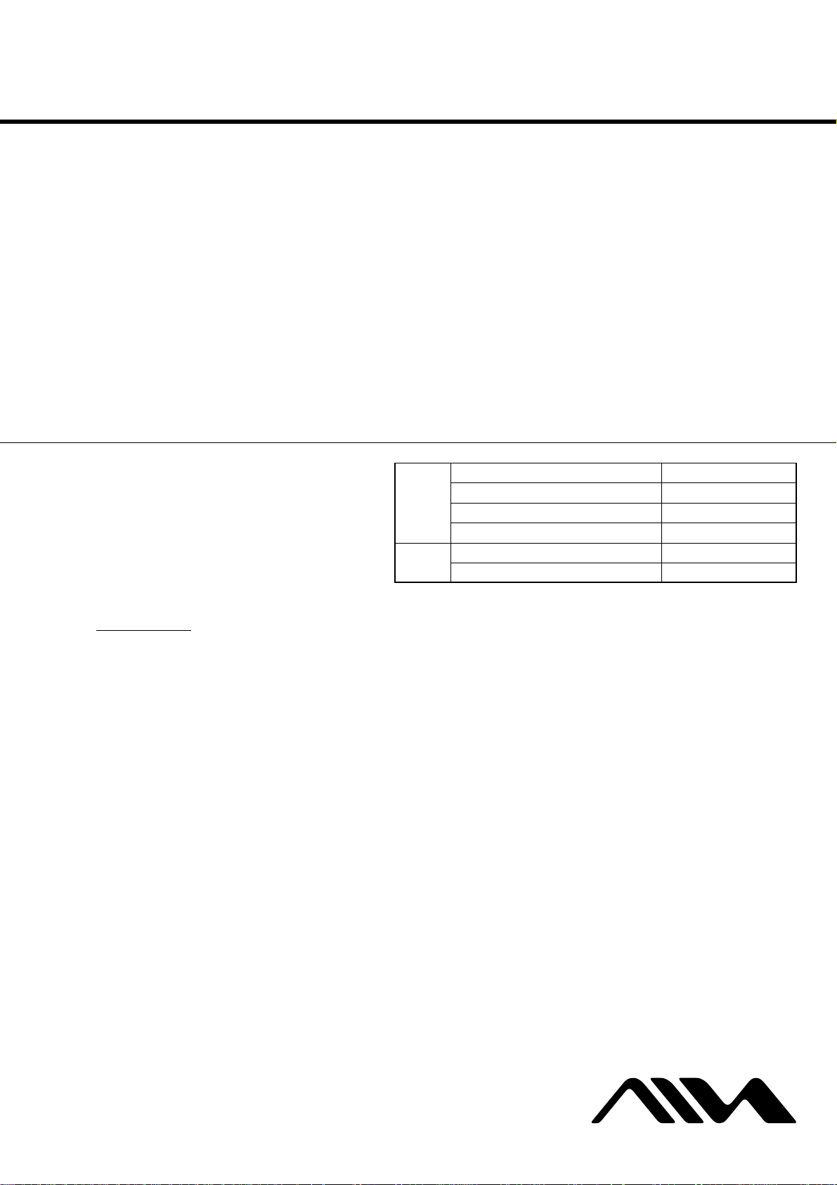
Power requirements 230 V AC, 50/60 Hz (AEP, UK)
120 V AC, 60 Hz (US, CND, TW)
120 V/220 V/230-240 V AC,
50/60 Hz (E)
220 V AC, 50/60 Hz (KR)
110-240 V AC, 50/60 Hz (TH)
220-240 V AC, 50/60 Hz (SP)
240 V AC, 50/60 Hz (AUS, TW)
MAIN UNIT CX-LMN5
TUNER
AMPLIFIER
CASSETTE DECK
CD PLAYER
GENERAL
Specifications and external appearance are subject to change
without notice.
with ECO mode on: 0.26 W (EXCEPT E)
0.35W (E)
0.25 W (US,CND)
0.26 W (AEP,UK)
0.26 W(TH,KR)
0.35 W(OTHER)
with ECO mode off:15 W (EXCEPT E)
18 W(E)
16 W (US,CND)
15 W (AEP,UK)
18 W (TH,KR)
18 W (OTHER)
FM tuning range 87.5 MHz to 108 MHz
FM usable sensitivity (IHF) 16.8 dBf
FM antenna terminal 75 Ω (unbalanced)
AM tuning range 531 kHz to 1602 kHz (9 kHz Step)
(AEP, UK)
AM usable sensitivity 350 µV/m
AM antenna Loop antenna
Power output Rated: 64 W + 64 W (6 Ω, T. H .D.
1 %, 1 kHz/DIN 45500)
Reference: 80 W + 80 W (6 Ω, T.H . D.
10 %, 1 kHz/DIN 45324)
MUSIC POWER: 220 W + 220 W
Input AUX IN: 1.4 V
Outputs SPEAKERS: 6 Ω or more
PHONES: 32 Ω or more
Track format 4 tracks, 2 channels stereo
Frequency response 100 Hz – 10000 Hz
Recording system AC bias
Heads Recording/playback × 1, erase × 1
Laser Semiconductor laser (λ = 800 nm)
Emission duration: continuous
D/A converter 1 bit dual
Signal-to-noise ratio 85 dB (1 kHz, 0 dB)
Wow and flutter Unmeasurable
Power consumption 85 W (EXCEPT US, CND)
Power consumption in standby mode
Dimensions (w/h/d) Approx. 190 × 277 × 353 mm
Mass Approx. 6.8 kg
Supplied accessories: FM antenna (1)
AM antenna (1)
Speaker cords (2)
Remote commander (1)
Batteries (2)
530 kHz to 1710 kHz (10kHz Step)
(EXCEPT AEP, UK)
531 kHz to 1710 kHz (9kHz Step)
(EXCEPT AEP, UK)
80 W (US, CND)
SERVICE MANUAL
Ver 1.2 2003.09
CX-LMN5 is the Amplifier, CD player, Tape
Deck and Tuner section in XR-MN5.
Model Name Using Similar Mechanism NEW
CD
Section
TAPE
Section
CD Mechanism Type CDM69BV-30CBD64NS
Base Unit Name BU-30CBD64NS
Optical Pick-up Name A-MAX.3
Model Name Using Similar Mechanism NEW
Tape Transport Mechanism T ype CMAL1Z240A
US Model
Canadian Model
AEP Model
UK Model
E Model
Australian Model
9-877-183-03
2003I16-1
© 2003.09
Sony Corporation
Home Audio Company
Published by Sony Engineering Corporation
SPECIFICATIONS
MICRO HI-FI COMPONENT SYSTEM
•Abbreviation
AUS: Australian model.
CND : Canadian model.
SP : Singapore model.
TW : Taiwan model.
KR : Korean model.
TH : Thai model.
Page 2

CX-LMN5
TABLE OF CONTENTS
1. SERVICING NOTES ······················································· 3
2. GENERAL ·········································································· 4
3. DISASSEMBLY
3-1. Side Panel (L)(R), Top Panel, Back Panel ······················ 7
3-2. CD Mechanism Section ·················································· 7
3-3. Front Panel Section ························································· 8
3-4. FRONT Board································································· 8
3-5. Cassette Deck Mechanism ·············································· 9
3-6. Cassette Panel ································································· 9
3-7. Power Transformer························································ 10
3-8. MAIN Board Section ···················································· 10
3-9. CD Mechanism Deck (CDM69BV-30CBD64NS) ······· 11
3-10. Base Unit Section························································ 11
3-11. Base Unit (BU-30CBD64NS) ····································· 12
3-12. BD Board ···································································· 12
3-13. SW Board, Bracket (TOP) Assy ································· 13
3-14. CONNECTOR Board ················································· 13
3-15. Motor (Stocker) Assy (Stocker)(M761)······················ 14
3-16. Motor (Roller) Assy (Roller)(M781) ·························· 14
3-17. Motor (Mode) Assy (Mode)(M771) ··························· 15
3-18. Rubber Roller (Slider) Assy········································ 15
3-19. Timing Belt (Front/Rear) ············································ 16
3-20. Cam (Gear) ································································· 16
3-21. SENSOR Board ·························································· 17
4. ASSEMBLY
4-1. How to Install the Cam (EJECT LOCK) ············ 18
4-2. How to Install the Cam (GEAR) ························ 18
4-3. How to Install the Gear (MODE C) ··················· 19
4-4. How to Install the Gear (MODE CAM) ············· 19
4-5. How to Install the Rotary Encoder (S702),
Gear (STOCKER COMMUNICATION) ··········· 20
4-6. How to Install the Stocker Assy ························· 20
5. TEST MODE ···································································· 21
6. MECHANICAL ADJUSTMENTS ····························· 22
8. DIAGRAMS······································································ 27
8-1. Block Diagram — BD, Changer Section — ·················28
— Main Section —······························ 29
8-2. Printed Wiring Boards — BD Section — ····················· 30
8-3. Schematic Diagram — BD Section — ························· 31
8-4. Printed Wiring Boards — Changer Section — ············· 32
8-5. Schematic Diagram — Changer Section — ················· 33
8-6. Printed Wiring Boards — Front Section — ·················· 34
8-7. Schematic Diagram — Front Section — ······················ 35
8-8. Printed Wiring Boards — Main Section — ·················· 36
8-9. Schematic Diagram — Main Section 1 — ··················· 37
8-10. Schematic Diagram — Main Section 2 — ················· 38
8-11. Schematic Diagram — Main Section 3 — ················· 39
8-12. Schematic Diagram — Main Section 4 — ················· 40
8-13. Schematic Diagram — Main Section 5 — ················· 41
8-14. Schematic Diagram
— Main Section 6/Power Section — ··············· 42
8-15. Printed Wiring Boards — Power Section — ············· 43
8-16. IC Block Diagrams ····················································· 44
8-17. IC Pin Function Description ······································· 47
9. EXPLODED VIEWS
9-1. Panel Section································································· 49
9-2. Front Section ································································· 50
9-3. Chassis Section ····························································· 51
9-4. CD Mechanism Deck Section 1
(CDM69BV-30CBD64NS) ··········································· 52
9-5. CD Mechanism Deck Section 2
(CDM69BV-30CBD64NS) ··········································· 53
9-6. CD Mechanism Deck Section 3
(CDM69BV-30CBD64NS) ··········································· 54
9-7. CD Mechanism Deck Section 4
(CDM69BV-30CBD64NS) ··········································· 55
9-8. CD Mechanism Deck Section 5
(CDM69BV-30CBD64NS) ··········································· 56
9-9. CD Mechanism Deck Section 6
(CDM69BV-30CBD64NS) ··········································· 57
9-10. CD Mechanism Deck Section 7
(CDM69BV-30CBD64NS) ··········································· 58
9-11. Optical pick-up Section ·············································· 59
7. ELECTRICAL ADJUSTMENTS ······························· 22
SAFETY-RELATED COMPONENT WARNING!!
COMPONENTS IDENTIFIED BY MARK 0 OR DOTTED LINE WITH
MARK 0 ON THE SCHEMATIC DIAGRAMS AND IN THE PARTS
LIST ARE CRITICAL TO SAFE OPERATION. REPLACE THESE
COMPONENTS WITH SONY PARTS WHOSE PART NUMBERS
APPEAR AS SHOWN IN THIS MANUAL OR IN SUPPLEMENTS
PUBLISHED BY SONY.
2
10.ELECTRICAL PARTS LIST ······································· 60
ATTENTION AU COMPOSANT AYANT RAPPORT
À LA SÉCURITÉ!
LES COMPOSANTS IDENTIFÉS PAR UNE MARQUE 0 SUR LES
DIAGRAMMES SCHÉMATIQUES ET LA LISTE DES PIÈCES SONT
CRITIQUES POUR LA SÉCURITÉ DE FONCTIONNEMENT. NE
REMPLACER CES COMPOSANTS QUE PAR DES PIÈSES SONY
DONT LES NUMÉROS SONT DONNÉS DANS CE MANUEL OU
DANS LES SUPPÉMENTS PUBLIÉS PAR SONY.
Page 3
CX-LMN5
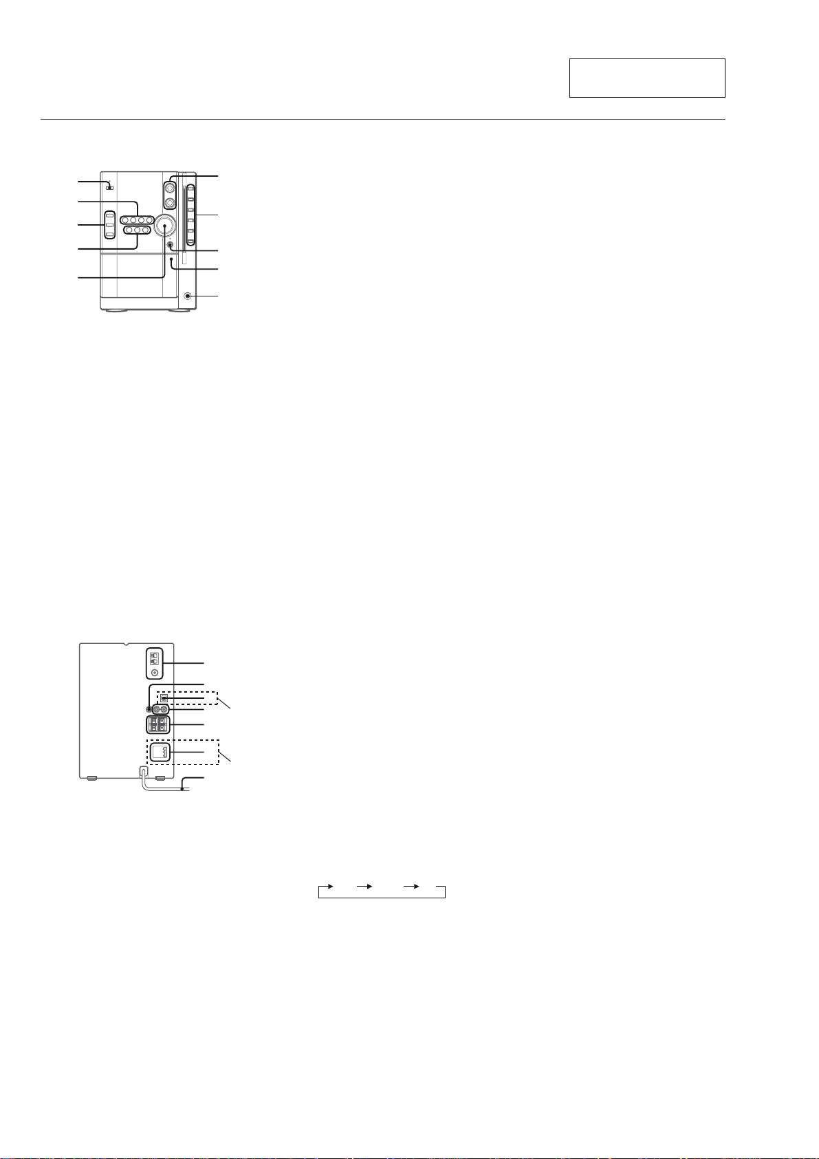
PARTS AND CONTROLS
Main unit: front
Refer to the pages indicated in parentheses for details.
1
2
3
4
5
1 POWER 6STANDBY/ON (8)
Switches the unit on and off (standby).
2 ECD (8, 10-12)
Starts and pauses CD play.
TUNER/BAND (8, 14)
Selects tuner function and the tuner band.
dTAPE (REC MUTING) (8, 17, 19)
Starts playback and changes the playback side.
Also used to enter 4-second blank spaces during
recording.
AUX (8)
Selects the function of external equipment connected to
AUX IN jacks.
6
7
8
9
0
SECTION 2
GENERAL
3 ECO/RDS (8, 14-16)
Sets the ECO mode on or off.
Tuner: Activates RDS features.
SYNCHRO REC (18)
Starts recording and CD play simultaneously.
REC START/REC PAUSE (18-20)
Starts and pauses recording.
4 s (10-12, 17, 18, 20)
CD and Tape: stops playback.
Tuner: clears a preset station.
TUNING f/r-, +t/g(8,10-12,
14, 17, 21, 22)
CD: skips to a previous or a succeeding track when
pressed, searches a track in fast forward or reverse
playback when held down.
Tape: rewinds or fast forwards the tape.
Tuner: manually tunes up or down within the band.
5 VOLUME (9)
Adjusts the volume.
6 TREBLE (9)
Adjusts the treble level.
BASS (9)
Adjusts the bass level.
7 zCD EJECT (10, 12)
Ejects the disc(s).
CD slot buttons (1-5) (8, 10-12)
Selects a disc slot.
Starts CD play for one desired disc.
This section is extracted
from instruction manual.
8 i-Bass/DEMO (4, 9)
Produces rich and clear low frequency sound.
Switches DEMO on and off while the unit is turned off.
9 PUSH EJECTz (17-19)
Opens or closes the cassette holder.
0 PHONES jack
Plug in optional headphones set with a stereo mini plug
(ø3.5 mm). Speaker output is cancelled.
Main unit: rear
Refer to the pages indicated in parentheses for details.
1
2
3
4
(AEP,UK)
5
120V
230-240V
220V
7
6
(E)
1 AM LOOP jack and FM 75 terminal (4)
Plug in the supplied AM and FM antennas.
2 SUB WOOFER3 jack
Connect optional powered sub woofer with a built-in
amplifier to the jack.
3 DIGITAL OUT (OPTICAL) jack (AEP, UK)
CD digital sound signals can be output through this jack.
Use an optical cable to connect digital audio equipment.
Fit an optical cable plug in the DIGITAL OUT (OPTICAL)
jack and push it to connect.
4 AUX IN jacks
Accept analogue sound signals from external equipment.
Connect external equipment using an optional connecting
cable with RCA phono plugs (red plug to R jack, white
plug to L jack). Refer also to the operating instructions
for your equipment.
To switch function to external input, press AUX.
To change a source name in the display of the
AUX function.
Hold down AUX and press POWER while the power is
on.
AUX VIDEO TV
5 SPEAKERS3 terminals (4)
Connect the speaker cords of the supplied speakers.
6 AC power cord (4)
7 VOLTAGE SELECTOR (E)
120 V/220 V/230-240 V AC,50/60Hz
4
Page 4
CX-LMN5
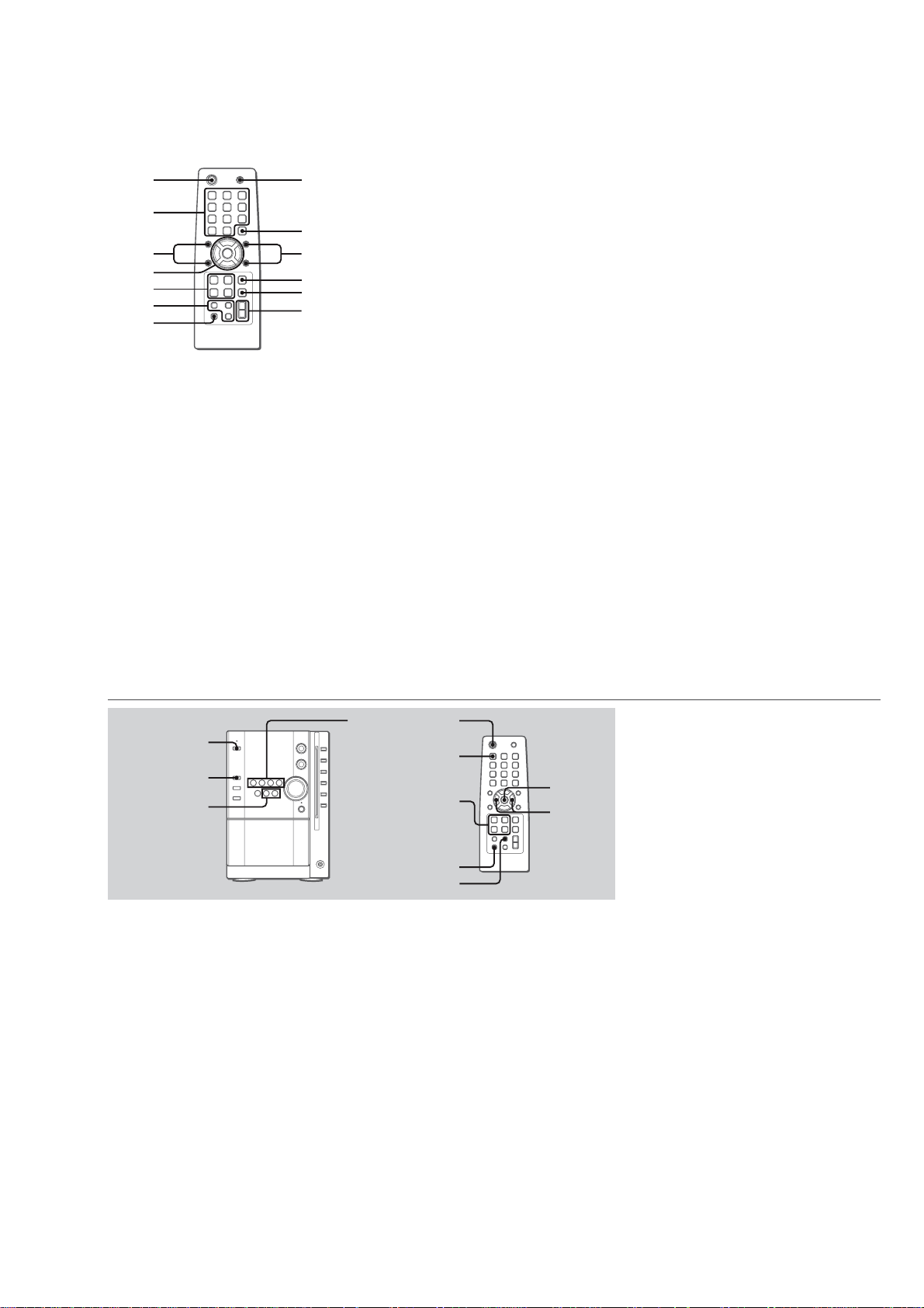
Remote commander
Refer to the pages indicated in parentheses for details.
1
2
3
4
5
6
7
Buttons with the same or similar names on the main unit
basically have the same function.
1 POWER (8)
2 1–10/0, >10 (10-12, 15, 19, 20)
CD: selects a track of the specified number.
Tuner: tunes in the station with the specified preset
number.
The numbered buttons take on these functions when pressed with
SHIFT held down
CLOCK (8)
Selects clock mode.
TIMER (21, 22)
Selects timer mode.
MUTING (9)
To turn off the sound temporarily.
:
8
9
0
!
@
#
TUNER MODE (15)
Switches between stereo or monaural FM reception.
REV MODE (17, 18, 22)
Selects a reverse mode.
DISC/ALBUM (12)
Selects disc mode or album mode on an MP3-CD.
CD EDIT/CHECK (19, 20)
Selects edited CD recording.
3 SHUFFLE/PROGRAM (11)
Selects shuffle or programmed CD playback mode.
REPEAT (11)
Selects repeat CD playback mode.
4 ALBUM/PRESETN,M (12, 15)
MP3-CD:Skips to a previous or succeeding album.
Tuner: Tunes in a preset station.
f/r,t/g (8, 10-12, 14, 17, 21,
22)
ENTER (8, 14, 15, 21, 22)
Determines the mode.
Stores the received station to preset.
5 ECD (8, 10-12)
TUNER/BAND (8, 14)
dTAPE (8, 17)
AUX (8)
6 DISPLAY (10, 12)
Changes the display in CD playback mode.
DIMMER (8)
Adjusts the display window brightness.
SLEEP (21)
Selects sleep-timer mode.
7 SHIFT
Hold down when pressing a numbered button to change
its function to that printed above the number.
8 DISC SELECT (10, 12)
Selects a desired CD slot.
9 CLEAR (11, 15, 21, 22)
CD: Clears a CD program
Tuner: Clears a preset station.
0 i-Bass (9)
TONE (9)
Selects the bass or treble adjusting mode.
! s (10-12, 17, 18, 20)
@ FUNCTION (18-20)
Switches the active function among TAPE, TUNER, AUX
(VIDEO or TV) and CD.
# VOLUME +,- (9)
ADJUSTMENTS BEFORE OPERATION
POWER
6STANDBY/ON
∗ ECO/RDS
m ,M
∗ AEP,UK : ECO/RDS
EXCEPT
AEP,UK : ECO
Power
Turning the unit on
Press POWER 6STANDBY/ON (POWER on the remote ).
Alternatively, press dTAPE, TUNER/BAND, AUX, ECD
or one of the CD slot buttons (1-5). Playback will start
automatically if a disc or tape is loaded.
Turning the unit off
Press POWER 6STANDBY/ON again.
The unit goes into standby.
Dimmer
The display window brightness can be selected.
Press DIMMER on the remote.
Each press of the button changes between darker and brighter.
u CD,
TUNER/
BAND,
Y TAPE,
AUX
POWER
CLOCK
u CD,
TUNER/
BAND,
Y TAPE,
AUX
SHIFT
DIMMER
ECO mode
Reduces power consumption in standby mode with the following
operations.
Press ECO/RDS. (AEP,UK : ECO/RDS EXCEPT AEP,UK : ECO)
Each press of the button changes the mode as follows;
ECO ON: Power economizing mode is activated.
When the unit turns off, everything on the display clears and
only the red indicator above POWER lights to show that the
power is being supplied.
ECO OFF: Power economizing mode is cancelled.
When the unit turns off, the clock display appears.
Initial mode is ECO OFF.
Standby power consumption
ECO ON: 0.26 W
ECO OFF: 15 W
ENTER
m ,M
Setting the clock
1
In stop mode, hold down SHIFT and press CLOCK
on the remote.
Go to step 3 when the hour of the clock display flashes.
2
Within 6 seconds, press ENTER.
The hour flashes in the display.
3
Press f or g to set the hour , then press
ENTER.
4
Press f or g to set the minute.
Each press changes the time in 1-minute steps.
5
Press ENTER.
The time display stops flashing and the clock starts from
00 seconds.
To display the time while the power is on
Hold down SHIFT and press CLOCK on the remote.
The time will be displayed for 6 seconds.
If " " appears when the unit is turned off
- -:- -
There has been a power interruption. Reset the clock.
5
Page 5
CX-LMN5
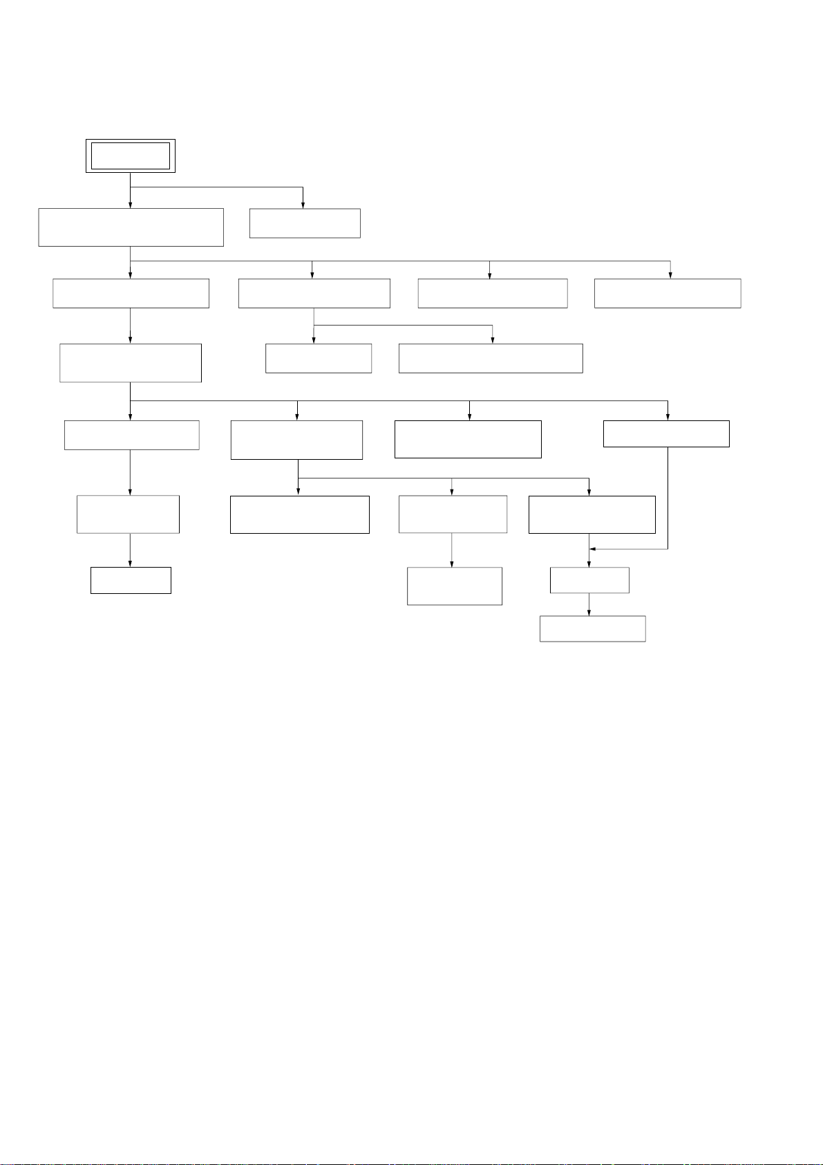
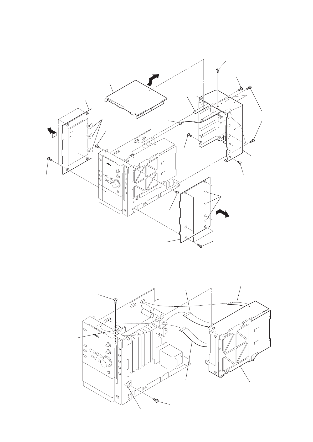
• This set can be disassembled in the order shown below.
SET
SECTION 3
DISASSEMBLY
SIDE PANEL (L) (R), TOP PANEL,
BACK PANEL
CD MECHANISM SECTION FRONT PANEL SECTION
CD MECHANISM DECK
(CDM69BV-30CBD64NS)
BASE UNIT SECTION
BASE UNIT
(BU-30CBD64NS)
BD BOARD
CASSETTE PANEL
FRONT BOARD CASSETTE DECK MECHANISM
SW BOARD,
BRACKET (TOP) ASSY
MOTOR (ROLLER)
ASSY (ROLLER) (M781)
POWER TRANSFORMER
MOTOR (STOCKER)
ASSY (STOCKER) (M761)
RUBBER ROLLER
(SLIDER) ASSY
TIMING BELT
(FRONT/REAR)
MAIN BOARD SECTION
CONNECTOR BOARD
MOTOR (MODE)
ASSY (MODE) (M771)
CAM (GEAR)
SENSOR BOARD
6
Page 6
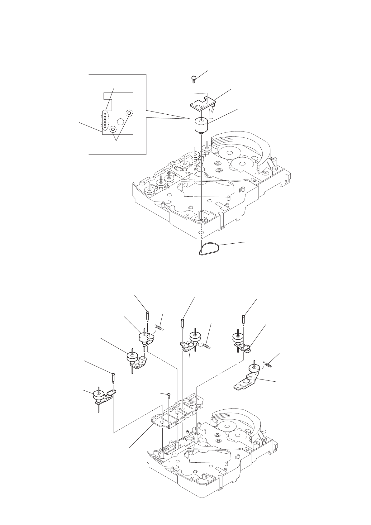
Note: Follow the disassembly procedure in the numerical order given.
n
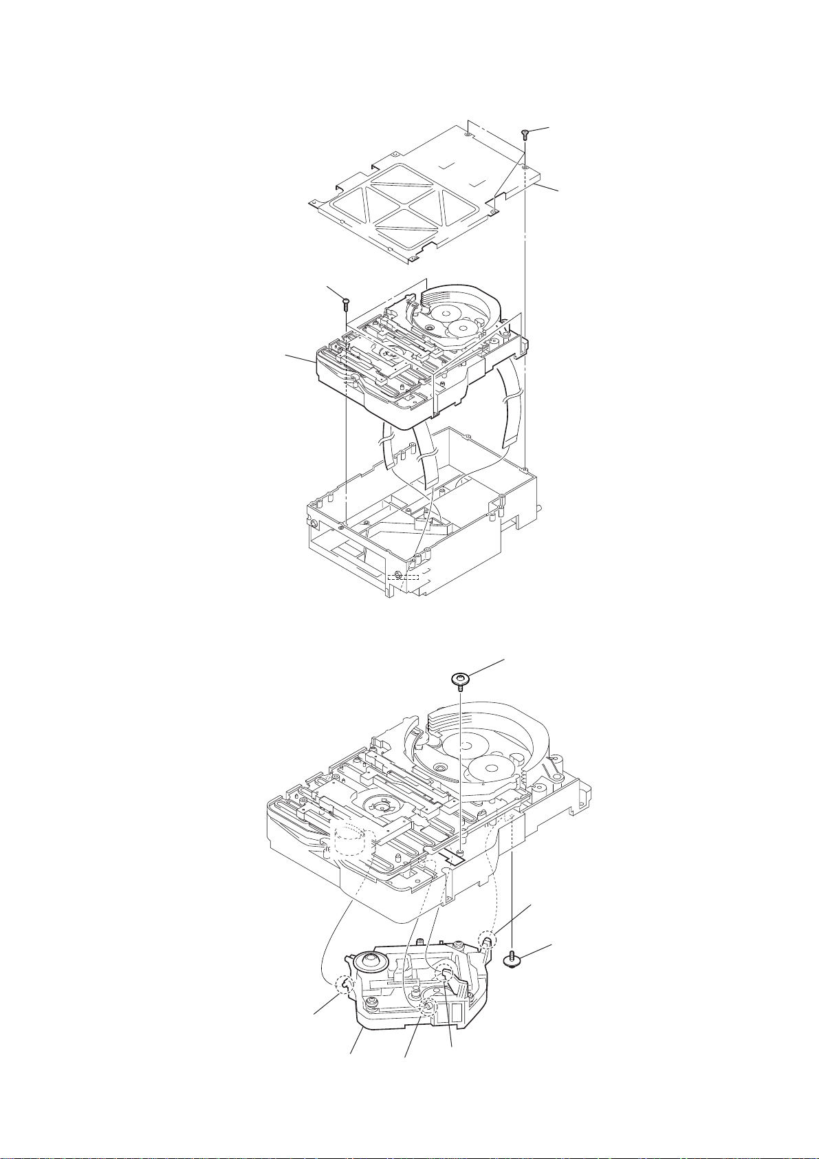
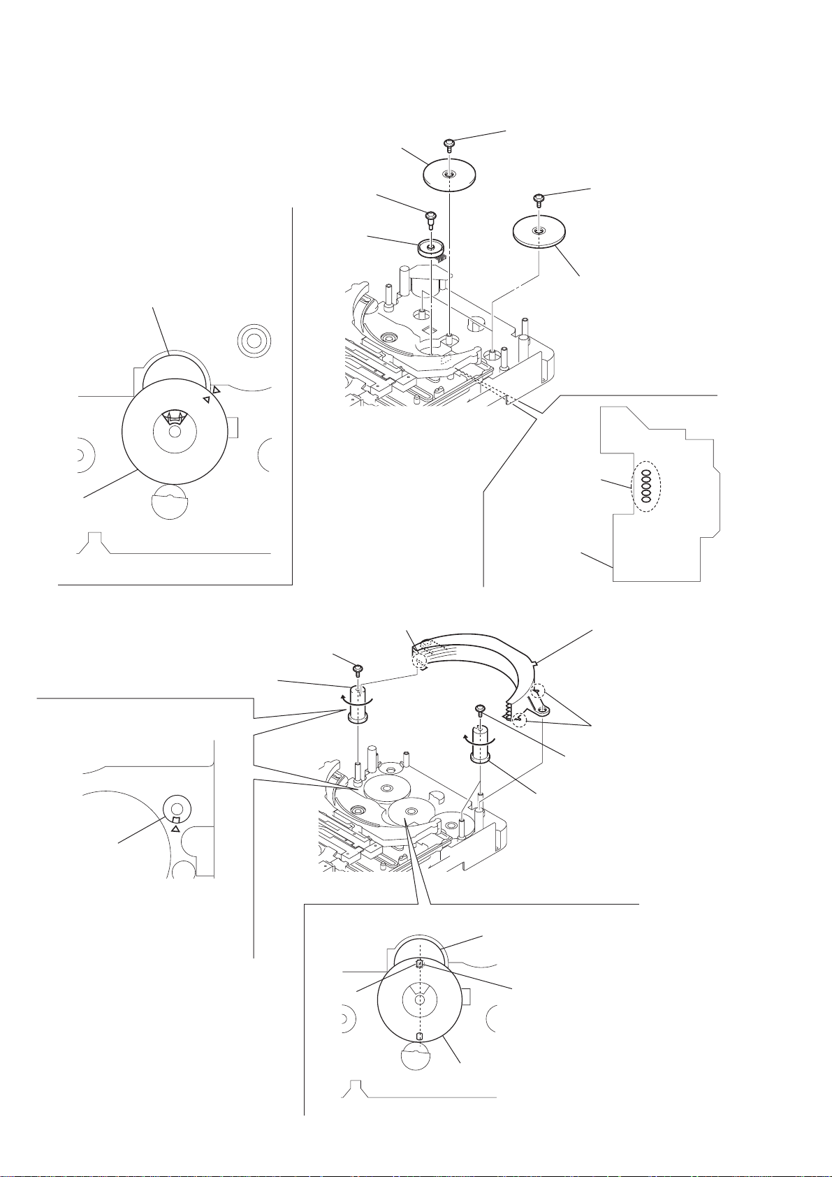
3-1. Side Panel (L)(R), Top Panel, Back Panel
q;
top panel
3
side panel (L)
2
three claws
9
screw
(QT2+3
×
10)
qa
connector
(CN293)
qh
w
ire (flat type)
15p /11P
(CN602)
qs
two screws
×
(QT2+3
10)
qf
screw
(+BVTP3
7
screw (+BVTP3 × 10)
qg
×
10)
ten screws
(+BVTP3
qj
back panel
CX-LMN5
×
10)
1
four screws
(+BVTP3
×
10)
3-2. CD Mechanism Section
4
screw
×
(QT2+3
10)
8
6
side panel (R)
screw
(QT2+3
2
27p (CN901)
×
10)
w
ire (flat type)
5
three claws
4
six screws
(+BVTP3
3
11p (CN601)
qd
three screws
(QT2+3
×
10)
w
ire (flat type)
×
10)
7
claw
6
claw
1
w
ire (flat type)
23p (CN902)
5
screw
×
(QT2+3
10)
8
CD mechanism sectio
7
Page 7
CX-LMN5
)
3-3. Front Panel Section
9
front panel section
7
screw
×
(QT2+3
10)
2
w
ire (flat type)
cassette deck mechanism
8p (
1
w
ire (flat type)
17p (CN904)
3
connector
(CN302)
)
8
two claws
3-4. FRONT Board
6
CD-KEY board
2
four claws
8
knob (VOL)
7
two knobs (BT)
6
screw
(QT2+3
1
screw
(+BVTP3
5
two screws
(+BVTP3
×
10)
×
10)
×
10)
q;
FRONT board
4
connector
(CN201)
9
nine screws
(+BVTP3
×
10
5
connector
(CN907)
4
panel (CD)
3
three claws
8
Page 8
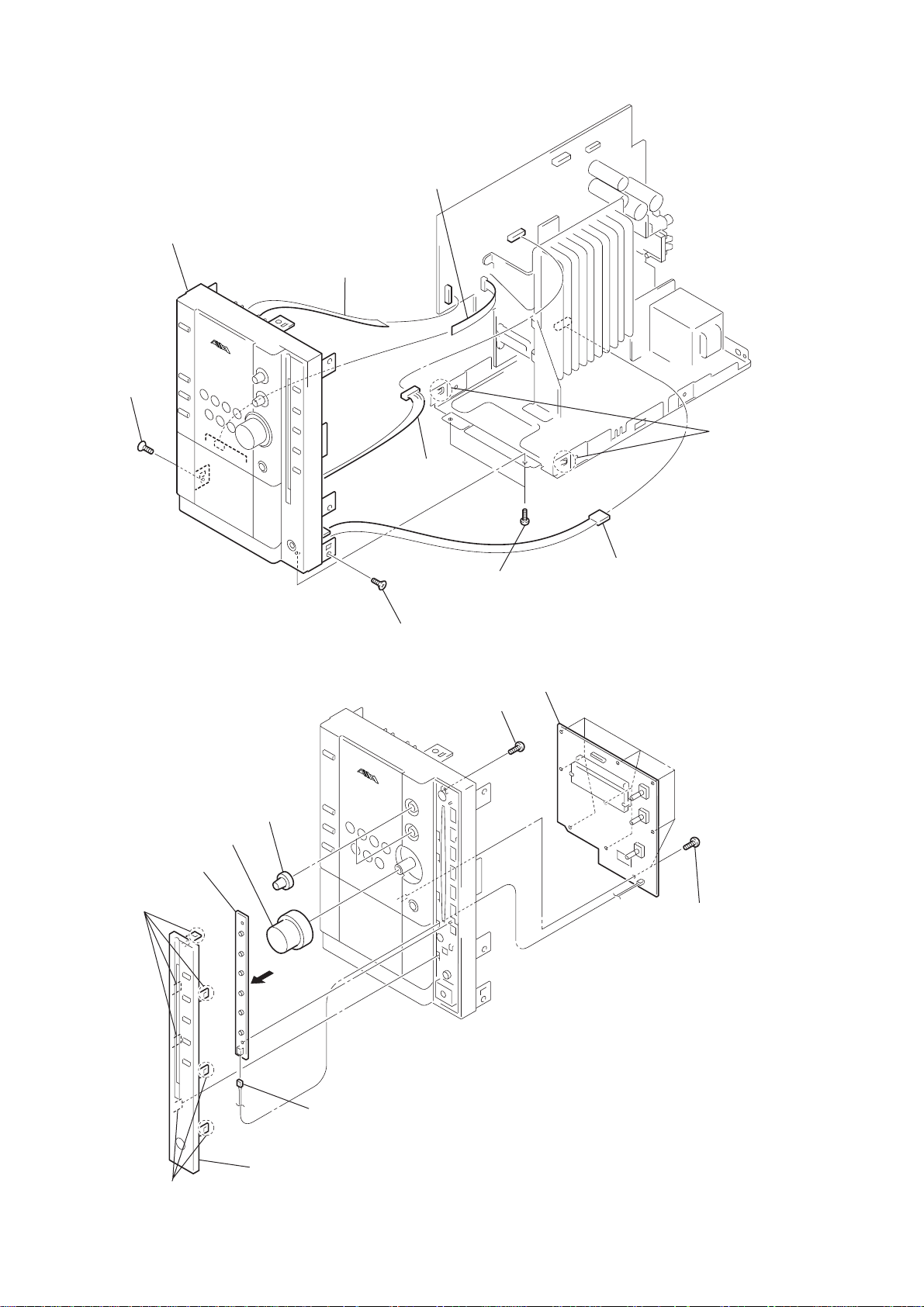
3-5. Cassette Deck Mechanism
)
4
cassette deck mechanism
3
three screws
(+BVTP3
×
10)
2
1
screw
(+BVTP3
shield (DECK)
CX-LMN5
×
10
3-6. Cassette Panel
2
1
3
claw
3
claw
4
cassette panel
9
Page 9
CX-LMN5
r
)
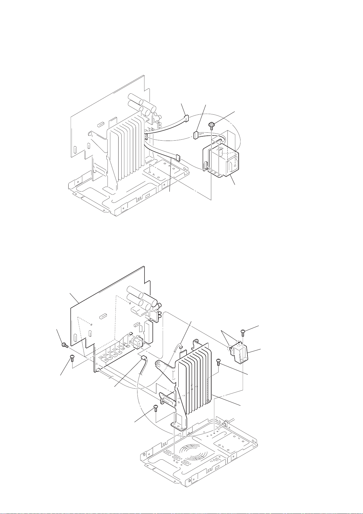
3-7. Power Transformer
4
connector
(CN256)
2
connector
(CN257)
3
connector
(CN252/ 254)
1
four s-screws
(ITC +4- 10R)
5
power transforme
3-8. MAIN Board Section
qa
MAIN board
9
four s-screws
(IT3B +3 - 8CU)
8
six screws
(+BVTP3
×
10)
1
connector
(CN202)
6
two screws
(BVIT3B+3- 8R W/O)
7
connector
(CN294)
3
two claws
2
screw
(BVIT3B+3- 8R W/O
4
holder (pwb.PT)
5
screw
(BVIT3B+3- 8R W/O)
q;
heat sink assy (MAIN)
10
Page 10
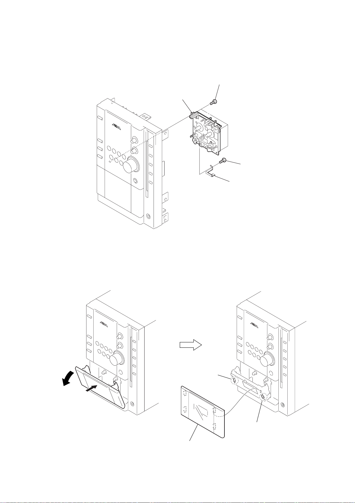
3-9. CD Mechanism Deck (CDM69BV-30CBD64NS)
)
)
3
four screws
(+BVTP3
4
CD mechanism deck
(CDM69BV-30CBD64NS)
×
10)
1
three screws
(QT2+3
2
holder(CD B
×
CX-LMN5
10)
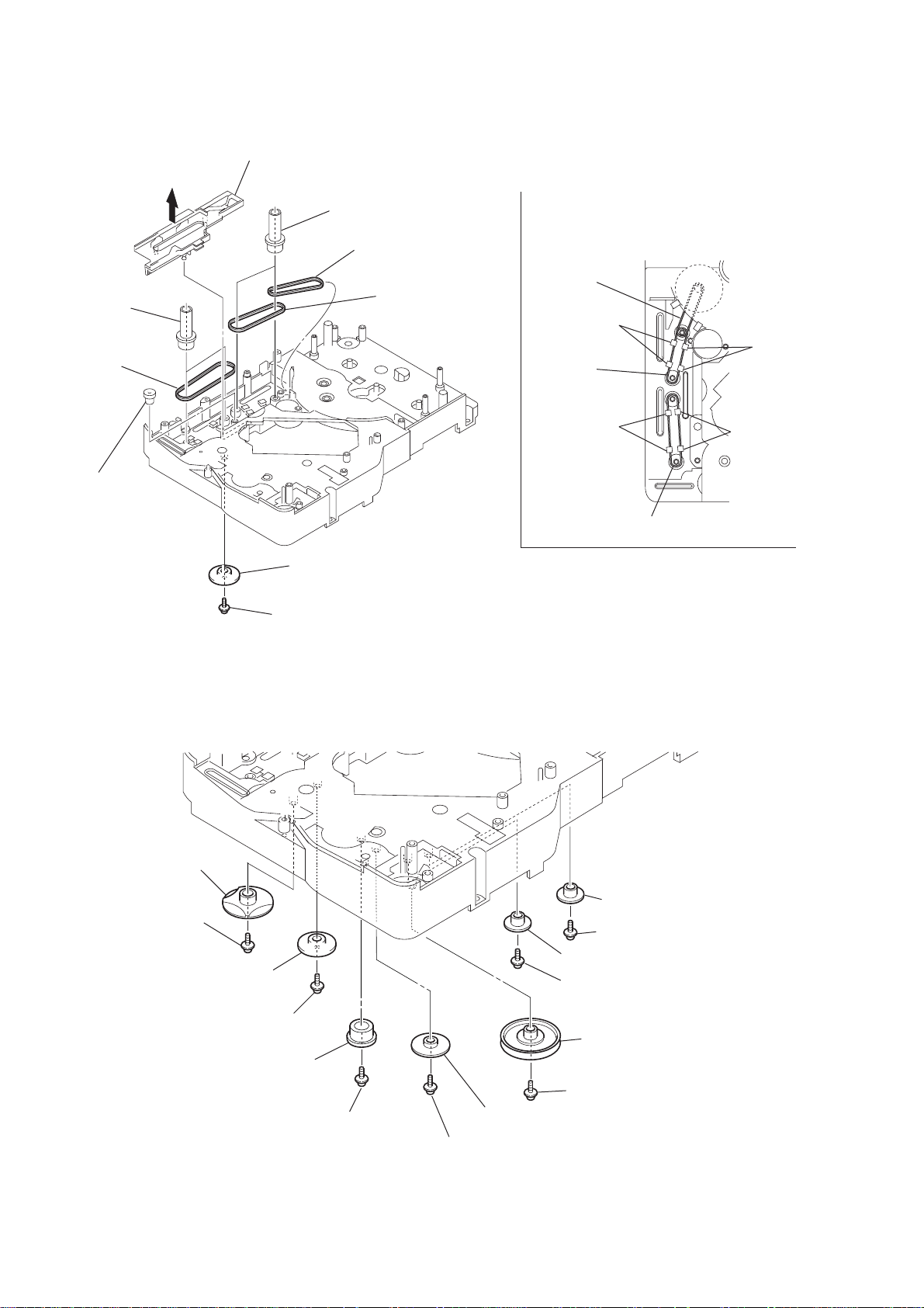
3-10. Base Unit Section
4
boss
2
screw
(+PTPWH) (M2) (DIA. 7)
3
boss
1
floating
screw
(DIA. 12
7
base unit section
5
boss
6
boss
11
Page 11
CX-LMN5
r
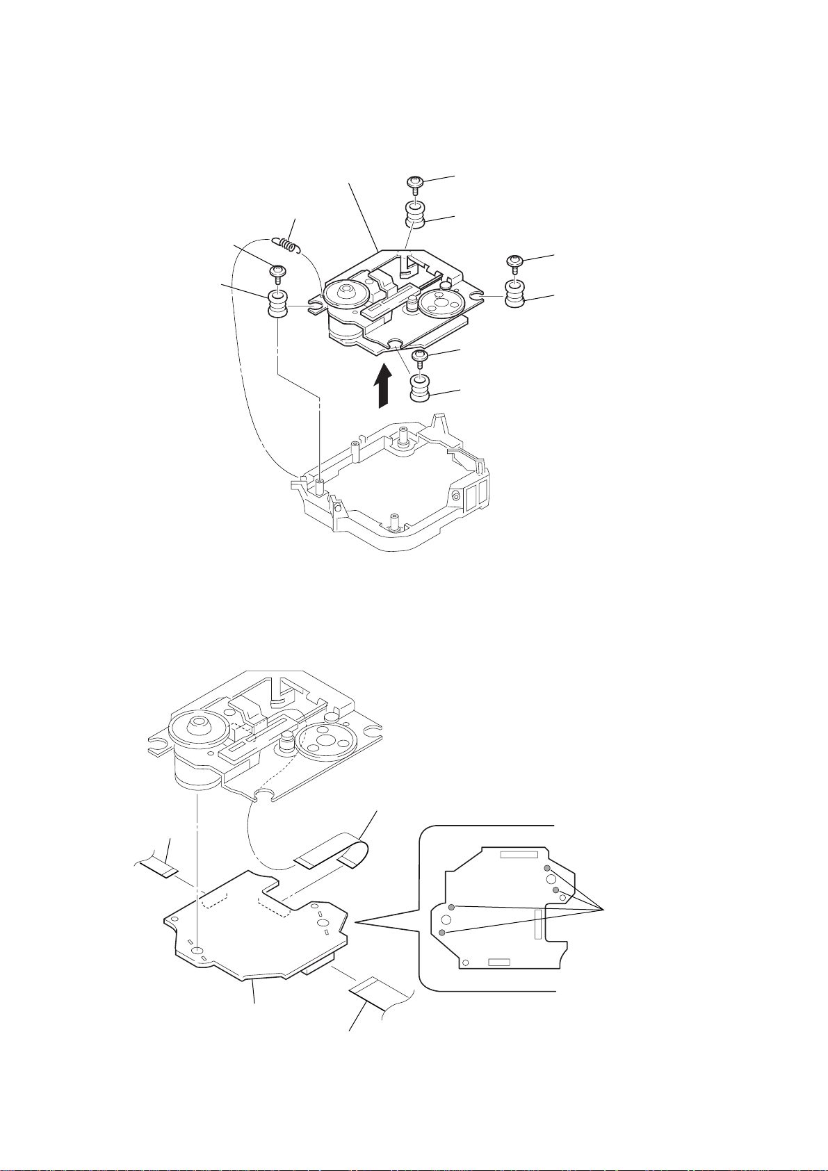
3-11. Base Unit (BU-30CBD64NS)
qa
1
tension spring (BU30-1)
5
floating screw
(+PTPWHM2.6
q;
vibration proof rubbers
×
6)
base unit (BU-30CBD64NS)
6
4
floating screw
(+PTPWHM2.6
9
vibration proof rubber
2
floating screw
(+PTPWHM2.6
7
vibration proof rubber
×
6)
3
floating screw
(+PTPWHM2.6
8
vibration proof rubber
×
6)
×
6)
3-12. BD Board
2
wire (flat type) (11 core)
5
BD board
4
wire (flat type) (16 core)
3
Remove the solde
(four portions).
12
1
wire (flat type) (23 core)
Page 12
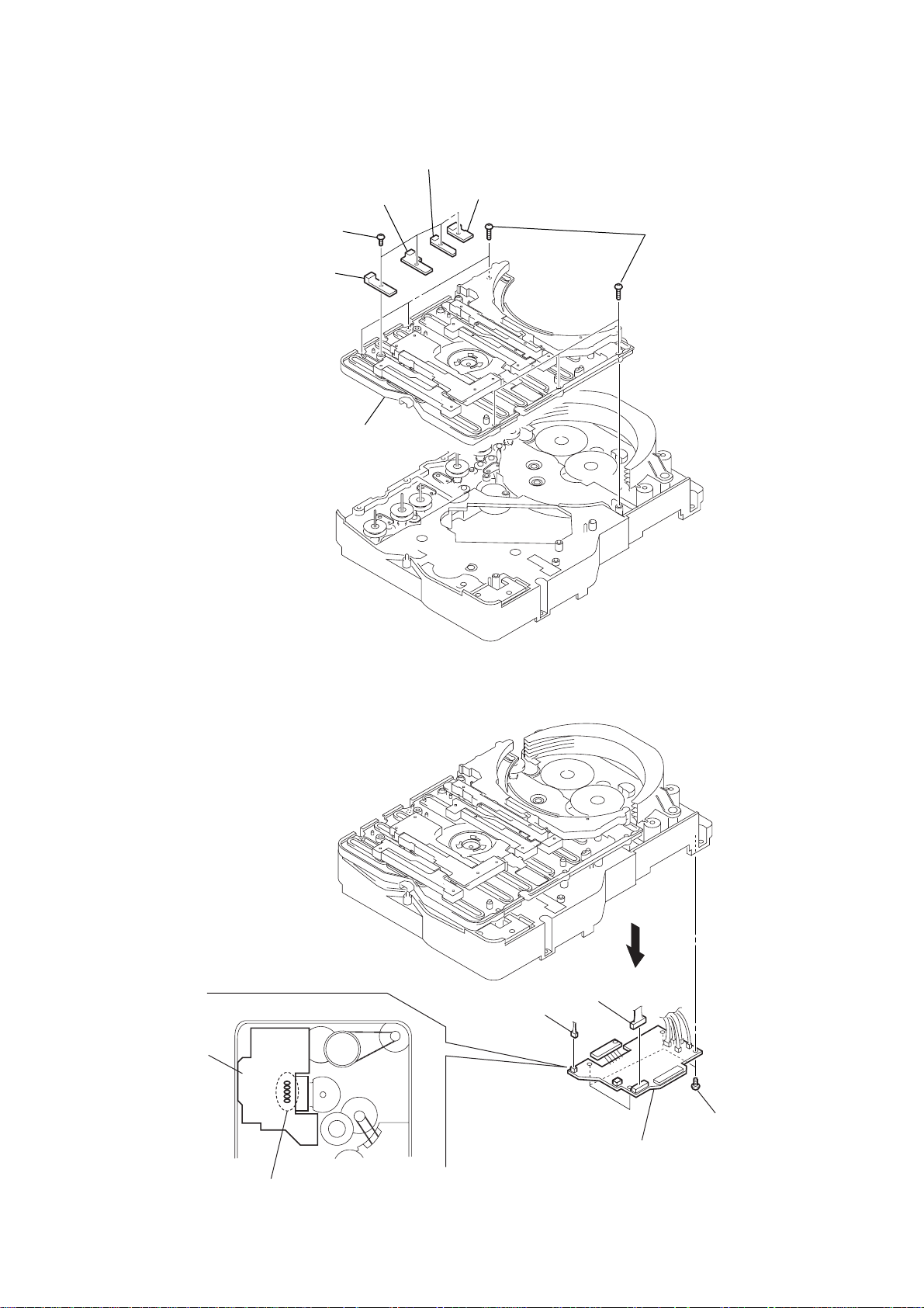
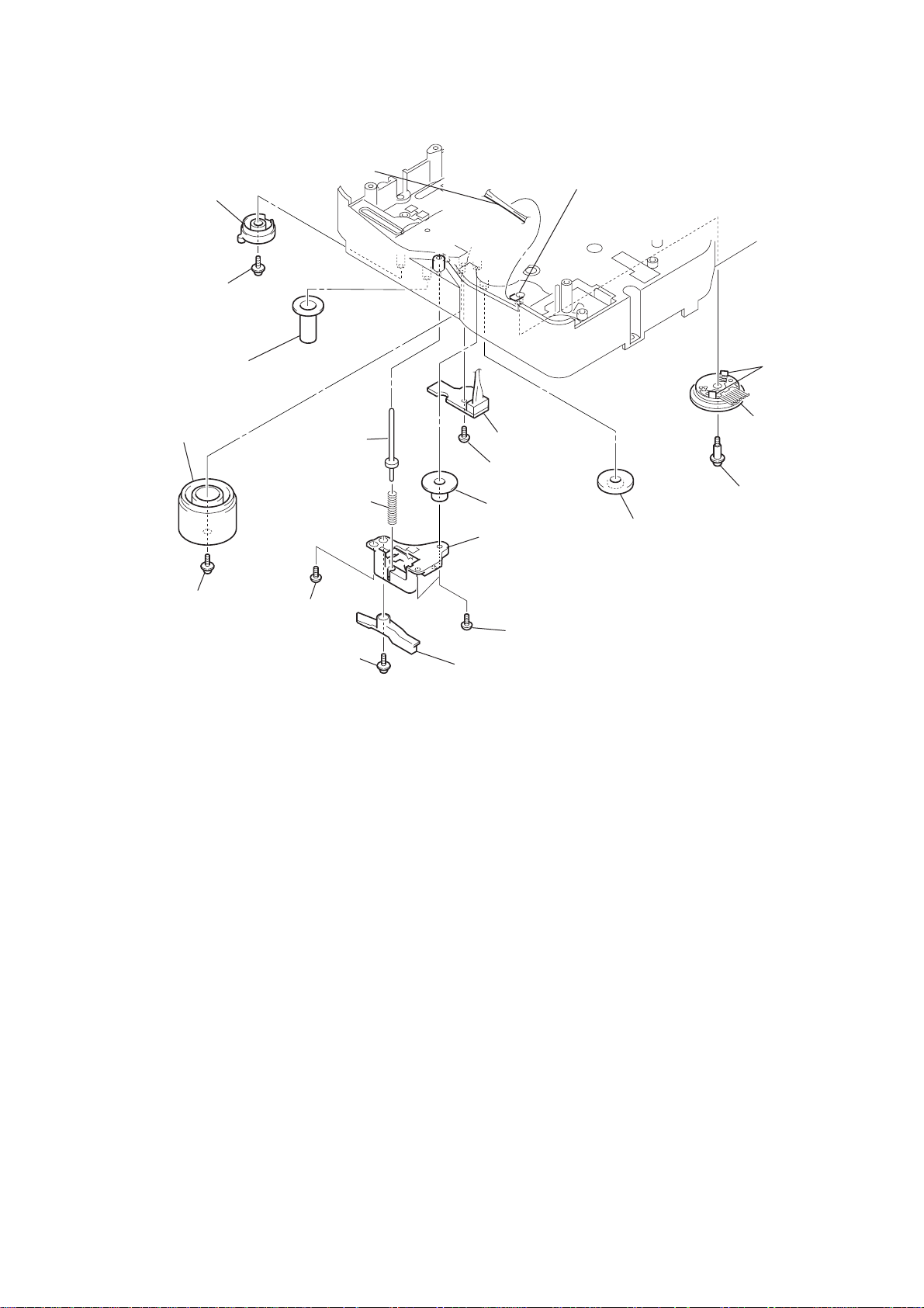
3-13. SW Board, Bracket (TOP) Assy
)
)
3
SW board (2)
1
four
screws
(BTP2.6
×
6)
2
SW board (1)
7
bracket (top) assy
4
SW board (3)
5
SW board (4)
6
six screws
(BVTP2.6
×
CX-LMN5
8
3-14. CONNECTOR Board
– bottom view –
CONNECTOR board
5
connector
(CN703)
4
connector
(CN710)
3
6
CONNECTOR board
2
four screws
(BVTP2.6
×
8
1
Remove five solders.
13
Page 13
CX-LMN5
s
d
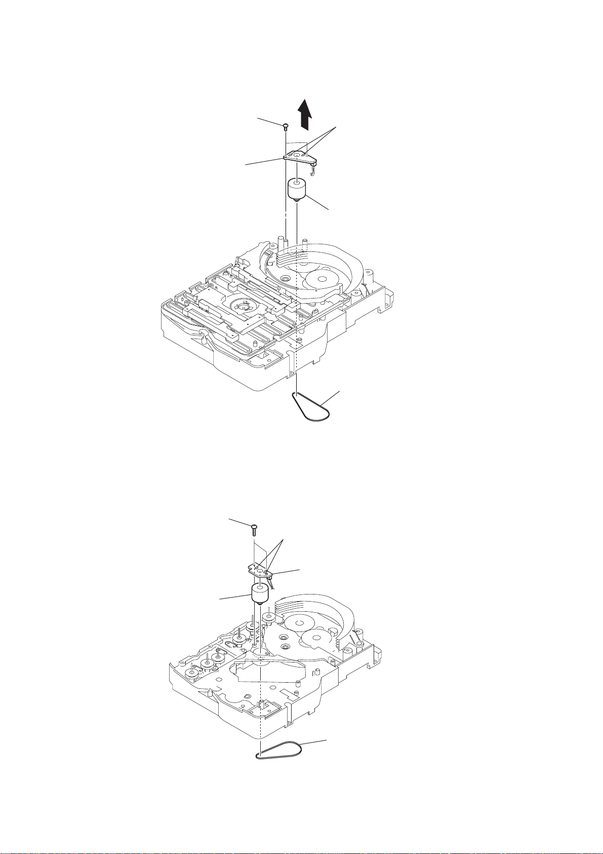
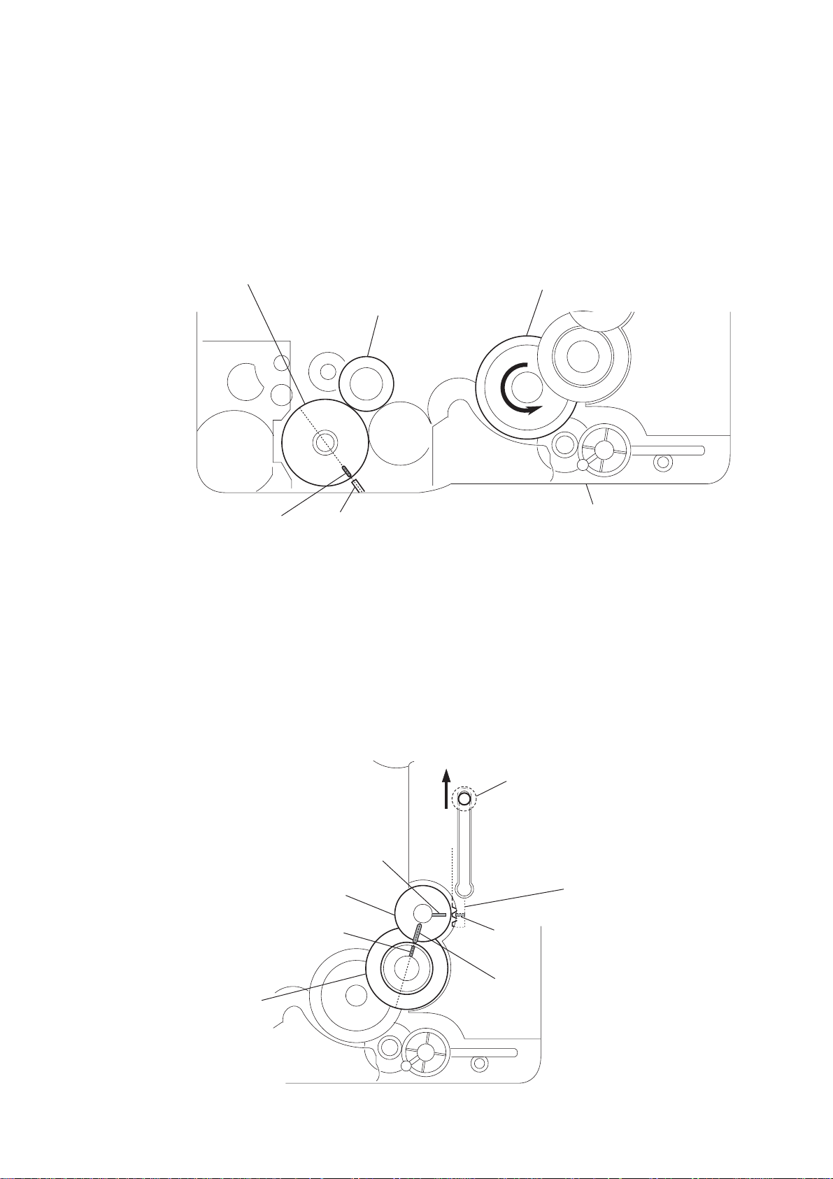
3-15. Motor (Stocker) Assy (Stocker)(M761)
3
two screws
(BVTP2.6
5
stocker motor board
×
4
8)
2
Remove two solder
6
motor (stocker) assy
(stocker) (M761)
1
belt (stocker)
3-16. Motor (Roller) Assy (Roller)(M781)
3
two screws
5
motor (roller) assy
(roller)(M781)
2
Remove two solders.
4
ROLLER MOTOR
1
belt (roller V)
boar
14
Page 14
3-17. Motor (Mode) Assy (Mode)(M771)
)
1
Remove five solders
of rotary encoder.
MODE MOTOR
board
2
Remove two solders
of motor (M771)
3
two screws
(BVTP2.6
×
8)
4
MODE MOTOR board
6
motor (mode) assy
(mode) (M771)
CX-LMN5
3-18. Rubber Roller (Slider) Assy
8
step screw
0
rubber roller
(slider 4) assy
qa
rubber roller
(slider 2) assy
qs
step screw
qd
rubber roller
(slider 1) assy
qf
screw
(BVTP2.6
9
×
tension
spring
(slider 2)
8)
5
step screw
6
tension spring
(base slider 4)
7
rubber roller
(slider 1) assy
5
belt (mode V)
1
step screw
2
rubber roller
(slider S) assy
3
4
tension spring
(base slider 5
rubber roller
(slider 5) assy
qg
sub chassis
15
Page 15
CX-LMN5
)
3-19. Timing Belt (Front/Rear)
3
5
two gears
(center)
6
timing belt
(front)
slider (mode cam) assy
7
two gears (center)
8
timing belt (rear)
9
timing belt (rear)
When install three timing belts,
its pass under each claws.
timing belt
(rear)
claw
timing belt
(rear)
claw
4
gear
(timing)
3-20. Cam (Gear)
qf
cam (gear)
: Note
2
gear (mode cam)
: Note
1
screw
(PTPWH2.6
×
claw
timing belt (front)
Note: Refer to assembly (Section 4)
8)
claw
16
qd
screw
qs
gear(mode cam)
qa
screw
(PTPWH2.6
0
Note: Refer to assembly
(Section 4).
×
8)
gear (mode C)
:Note
9
screw
(PTPWH2.6
6
gear (mode 5)
5
screw (PTPWH2.6 × 8
4
gear (mode 5)
3
screw (PTPWH2.6 × 8)
2
pulley
(mode deceleration)
1
screw(PTPWH2.6 × 8)
8
gear (mode D)
×
8)
7
screw (PTPWH2.6 × 8)
Page 16
3-21. SENSOR Board
ql
harness
qd
gear (eject lock)
q;
cam (eject lock)
: Note
qh
two claws
qj
rotary encoder
(S771)
qf
gear
(mode B)
w;
screw
(BVTP2.6
×
8)
qg
screw
(PTPWH2.6
×
8)
wa
SENSOR board
8
shaft
(shutter)
7
compression spring
(shutter)
qs
cam (BU U/D)
qa
screw
(PTPWH2.6
×
8)
3
screw
(BVTP2.6
×
8)
1
screw
(PTPWH2.6
×
8)
4
two screws
(BVTP2.6
×
8)
2
lever shutter (A)
5
base (shutter) block
6
gear (mode A)
9
screw
(PTPWH2.6
×
8)
qk
claw
Note: Refer to assembly (Section 4).
CX-LMN5
17
Page 17

CX-LMN5
• This set can be assembled in the order shown below.
4-1. How to Install the Cam (EJECT LOCK)
1
Rotate the cam (BU U/D) fully in the direction of arrow.
2
Engage the gear (eject lock) and the gear of the cam (eject lock)
aligning the mark with the center of the gear (eject lock).
cam (BU U/D)
SECTION 4
ASSEMBLY
mark
4-2. How to Install the Cam (GEAR)
1
Check that the cam (BU U/D) can not be rotated in the direction of arrow.
2
Align the mark on the cam (gear) with the boss as shown in the figure
and install the cam (gear).
cam (BU U/D)
gear (eject lock)
– bottom view • front –
cam (gear)
cam (eject lock)
boss
mark
18
– bottom view • front –
Page 18
4-3. How to Install the Gear (MODE C)
1
Align the mark on the rotary encoder (S771) with the projection of the assy.
2
Check that the cam (BU U/D) can not be rotated in the direction of arrow.
3
Install the gear (
rotary encoder
(S771)
mode
C)
gear (
mode
CX-LMN5
cam (BU U/D)
C)
mark projection
4-4. How to Install the Gear (MODE CAM)
1
Slide the shaft in the direction of arrow.
2
Align mark A on the gear (mode cam) with mark B on the slider (mode cam) assy,
then install the gear (mode cam).
3
Check that mark C on the gear (mode cam) is in alignment with mark D on the cam (gear).
mark
gear (mode cam)
chassis
– bottom view • front –
shaft
A
slider (mode cam) assy
cam (gear)
mark
D
– bottom view • front –
mark
mark
B
C
19
Page 19
CX-LMN5
4-5. How to Install the Rotary Encoder (S702), Gear (STOCKER COMMUNICATION)
4
Engage the rotary encoder (S702)
and the gear (stocker communication)
as shown below in the figure.
rotary encoder
(S702)
gear
(stocker communication)
3
screw
×
(PWH2
1
6)
rotary encoder
(S702)
5
screw
(PTPWH2.6
×
8)
7
two screws
(PTPWH2.6
6
two gears
(stocker communication)
×
8)
gear
(stocker
communication)
– rear –
4-6. How to Install the Stocker Assy
3
screw
(PTPWH2.6
2
cam
(stocker V)
cam
×
2
five
solders
CONNECTOR board
boss
8)
4
two cams
(stocker U/D)
Install the stocker assy
fitting three bosses into the
each groove of cam
then fix by rotating the cams
in the direction of arrow.
boss
5
two screws
(PTPWH2.6
×
8)
To install three cams, align each groove
of the cam with each
chassis as shown in the figure.
f
mark on the
20
screw
– rear –
rotary encoder
(S702)
hole
1
Position the hole on the gear
(stocker communication) on the
screw of the rotary encoder (S702).
gear
(stocker communication)
Page 20

SECTION 5
TEST MODE
CX-LMN5
[Cold Reset]
* The cold reset clears all data including preset data stored in the
RAM to initial conditions. Execute this mode when returning
the set to the customer.
Procedure:
1. Press the POWER button to turn off the main power.
2. While depressing the x button, press the POWER button.
3. The fluorescent indicator tube does not display any message
and the set is reset.
[Version Display Mode]
*The version of the microcomputer is displayed.
Procedure:
1. Press the POWER button to turn the set on.
2. To enter the test mode, press two buttons x and POWER
simultaneously for more than five seconds. The version of the
microcomputer is displayed.
[FL Tube Check]
* All fluorecent segments are tested.
Procedure:
1. Insert a disc, and extract an AC plug.
2. While depressing the u (CD) button, insert an AC plug to
enter the test mode.
3. The message “CD TEST” is displayed, the initialization is
performed.
Then all segments of the fluorecent indicator tube are turned on.
[CD Ship Mode]
*This mode moves the optical pick-up to the position durable to
vibration. Use this mode when returning the set to the customer
after repair.
Procedure:
1. Press the POWER button to turn the set on.
2. Set the FUNCTION to CD.
3. Press the x button for more than five seconds.
4. After a message “MECHA LOCK” is displayed on the
fluorescent indicator tube, the CD ship mode is set and the power
is turned off.
[AM Channel Step 9 kHz/10kHz Selection Mode]
* Either the 9 kHz step or 10 kHz step can be selected for the AM
channel step. (EXCEPT AEP,UK)
Procedure:
1. Set the FUNCTION to AM.
2. While depressing the TUNER button, press the POWER
button.
3. The channel step is changed over.
[CD Test Mode]
*This mode can run the CD sled motor freely. Use this mode, for
instance, when cleaning the pickup.
Procedure:
1. Extract an AC plug.
2. While depressing the u (CD) button, insert an AC plug to
enter the CD test mode. The message “CD TEST” is displayed.
3. With the CD in stop status, press the > button to move the
pickup to outside track, or press the . button to inside
track.
4. When press the u (CD) button, normal playback is
performed.
5. Each time the u (CD) button is pressed during normal
playback, the tracking servo is switched on or off.
6. To exit this mode, either change to other functions or extract
an AC plug.
[CD Repeat 5 Times Limit Release Mode]
Procedure:
1. Press the POWER button to turn the set on.
2. Select the FUNCTION to CD.
3. Press two buttons of > and u (CD) simultaneously.
4. The repeat all mark blinks and then repeat 5 times limit is
released.
[Disc Tray Lock]
The disc tray lock function for the antitheft of an demonstration
disc in the store is equipped.
Setting Procedure :
1. Press the POWER button to turn the set on.
2. Press two buttons of x and Z (CD EJECT) simultaneously
for five seconds.
3. The message “LOCKED” is displayed and the tray is locked.
Releasing Procedure :
1. Press two buttons of x and Z (CD EJECT) simultaneously
for five seconds again.
2. The message “UNLOCKED” is displayed and the tray is
unlocked.
Note : When “LOCKED” is displayed, the tray lock is not released
by turning power on/off with the POWER button.
[AMP Test]
*This mode is used to check the function of the amplifier.
Procedure:
1. Extract an AC plug.
2. While depressing the AUX button, insert an AC plug to enter
the AMP test mode. The message “AMP TEST” is displayed.
3. The message “Volume MAX” is displayed, when the VOLUME
knob is rotated clockwise. The message “Volume 0” is displayed,
when the VOLUME knob is rotated counterclockwise.
4. Each time the BASS or TREBLE knob is turned, the message
“EQ MAX”, “EQ MIN” or “EQ FLAT” is displayed in this
order.
21
Page 21
CX-LMN5
set
MAIN board
SPEAKER terminal (J201)
L-CH, R-CH
+
–
level meter
test tape
P-4-A100
(10 kHz, – 10 dB)
SECTION 6
MECHANICAL ADJUSTMENTS
SECTION 7
ELECTRICAL ADJUSTMENTS
• TAPE MECHANISM DECK SECTION
Precaution
1. Clean the following parts with a denatured alcohol-moistened
swab:
record/playback heads pinch rollers
erase head rubber belts
capstan idlers
2. Demagnetize the record/playback head with a head
demagnetizer.
3. Do not use a magnetized screwdriver for the adjustments.
4. After the adjustments, apply suitable locking compound to the
parts adjusted.
5. The adjustments should be performed with the rated power
supply voltage unless otherwise noted.
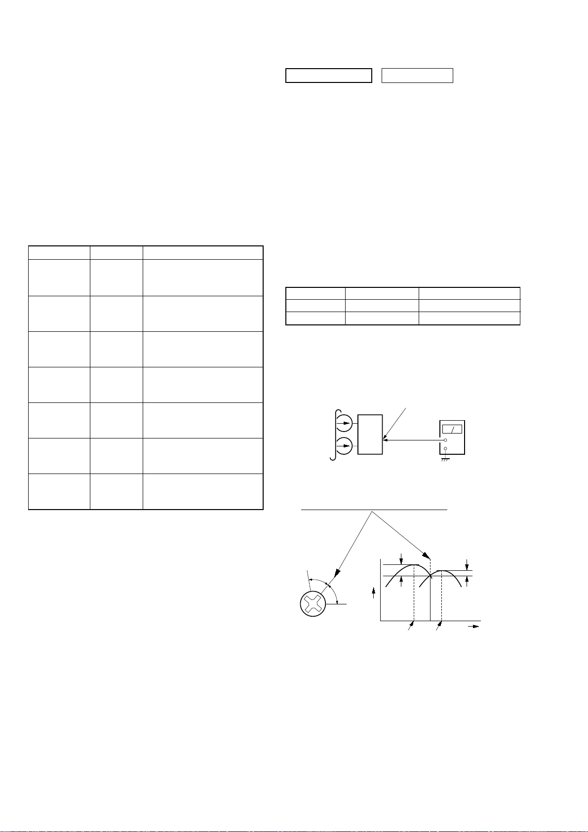
Torque Measurement
Mode
FWD
FWD
back tension
REV
REV
back tension
FF/REV
FWD tension
REV tension
Torque meter
CQ-102C
CQ-102C
CQ-102RC
CQ-102RC
CQ-201B
CQ-403A
CQ-403R
Meter reading
2.94 – 7.84 mN • m
(30 to 79 g • cm)
(0.42 – 1.11 oz • inch)
0.15 – 0.6 mN • m
2 to 6 g • cm
(0.03 – 0.08 oz • inch)
2.94 – 7.84 mN • m
(30 to 79 g • cm)
(0.42 – 1.11 oz • inch)
2.94 – 7.84 mN • m
(30 to 79 g • cm)
(0.42 – 1.11 oz • inch)
6.86 – 17.64 mN • m
(70 to 179 g • cm)
(0.98 – 2.49 oz • inch)
9.8 mN • m
(100 • cm or more)
(1.4 oz • inch or more)
9.8 mN • m
(100 • cm or more)
(1.4 oz • inch or more)
DECK SECTION
0 dB = 0.775 V
Precaution
1. Demagnetize the record/playback head with a head
demagnetizer.
2. Do not use a magnetized screwdriver for the adjustments.
3. After the adjustments, apply suitable locking compound to the
parts adjust.
4. The adjustments should be performed with the rated power
supply voltage unless otherwise noted.
5. The adjustments should be performed in the order given in this
service manual. (As a general rule, playback circuit adjustment
should be completed before performing recording circuit
adjustment.)
6. The adjustments should be performed for both L-CH and RCH.
7. Switches and controls should be set as follows unless otherwise
specified.
• Test Tape
Tape Signal Used for
P-4-A100 10 kHz, – 10 dB Azimuth Adjustment
WS-48B 3 kHz, 0 dB Tape Speed Check
Record/Playback Head Azimuth Adjustment
Procedure:
1. Mode: Playback
2. Turn the adjustment screw and check output peaks. If the peaks
do not match for L-CH and R-CH, turn the adjustment screw
so that outputs match within 1dB of peak.
22
L-CH
peak
Screw
position
R-CH
peak
Output
level
within
1dB
L-CH
peak
R-CH
peak
within
1dB
Screw
position
Page 22

CX-LMN5
+
–
set
recorded
portion
MAIN board speaker terminal (J201)
level meter
attenuator
set
MAIN board
AUX IN (J602)
1) 315 Hz
2) 10 kHz
50 mV (–23.8 dB)
600
Ω
blank tape
CN-123
AF OSC
SFR452
Record Bias
Adjustment(R-CH)
SFR451
Record Bias
Adjustment(L-CH)
IC601
IC901
3. Mode: Playback
MAIN board
test tape
P-4-A100
(10 kHz, – 10 dB)
L-CH
set
R-CH
in phase 45°90°135°180
SPEAKER terminal (J201)
L-CH
R-CH
waveform of oscilloscope
good
oscilloscope
wrong
H
V
°
4. After the adjustments, apply suitable locking compound to the
parts adjusted.
Adjustment Location: Record/Playback/Erase Head
Record Bias Adjustment
Procedure:
1. Record mode
2. Mode: Playback
i-Bass OFF
BASS 0
TREBLE 0
adjustment screw
Note: Refer to “3-6. Cassette Panel” (see page 9)
Tape Speed Check
Mode: Playback
test tape
WS-48B
(3 kHz, 0 dB)
3. Confirm playback the signal recorded in step 1 become
adjustment level as follows.
4. If these levels do not adjustment level, adjustment the SFR451
(L-CH) and SFR452 (R-CH) to repeat steps 1 and 4.
Adjustment level: Playback output of 315 Hz to playback output
of 10 kHz: 0 ± 1.0 dB (0 ± 4.5mV).
Adjustment Location: MAIN board
[MAIN BOARD] – Component Side –
frequency counter
1. Insert the WS-48B into the deck.
2. Press the N button on the deck.
3. Confirm that the frequency counter reads 3,000 ± 90 Hz.
Sample value of Wow and Flutter: 0.3% or less W.RMS (JIS)
set
MAIN board
SPEAKER terminal (J201)
L-CH, R-CH
(WS-48B)
+
–
23
Page 23

CX-LMN5
CD SECTION
Note:
1. Use YEDS-18 disc (3-702-101-01) unless otherwise indicated.
2. Use an oscilloscope with more than 10MΩ impedance.
3. Clean the object lens by an applicator with neutral detergent when the
signal level is low than specified value with the following checks.
S-curve Check
Connection:
oscilloscope
BD board
TP (FE)
TP (VC)
Procedure:
1. Connect an oscilloscope to test point TP (FE) and TP (VC)
on the BD board.
2. While depressing the (CD) button, insert an AC plug.
u
3. Put the disc (YEDS-18) in and press the (CD) button
and actuate the focus search. (actuate the focus search when
disc table is moving in and out)
4. Check the oscilloscope waveform (S-curve) is symmetrical
between A and B. And confirm peak to peak level within 2 ± 1
Vp-p.
S-curve waveform
+
–
symmetry
A
B
x
within 2
±
1 Vp-p
RFDC signal waveform
VOLT/DIV: 200 mV
TIME/DIV: 500 ns
level: 0.6
±
0.15 Vp-p
Checking Location: CD board (Conductor side)
RFAC Level Check
Connection:
oscilloscope
BD board
TP (RFAC)
TP (VC)
+
–
Procedure:
1. Connect an oscilloscope to test point TP (RFAC) and TP (VC)
on the BD board.
2. Turn the power on.
3. Put the disc (YEDS-18) in to playback the number five track.
4. Confirm that oscilloscope waveform is clear and check RFAC
signal level is correct or not.
Note: A clear RFAC signal waveform means that the shape “◊” can be
clearly distinguished at the center of the waveform.
RFAC signal waveform
VOLT/DIV: 200 mV
TIME/DIV: 500 ns
Note: •Try to measure several times to make sure than the ratio of A : B
or B : A is more than 10 : 7.
•Take sweep time as long as possible and light up the
brightness to obtain best waveform.
Checking Location: BD board (Side B)
RFDC Level Check
Connection:
oscilloscope
BD board
TP (RFDC)
TP (VC)
+
–
Procedure:
1. Connect an oscilloscope to test point TP (RFDC) and TP (VC)
on the BD board.
2. Turn the power on.
3. Put the disc (YEDS-18) in to playback the number five track.
4. Confirm that oscilloscope waveform is clear and check RFDC
signal level is correct or not.
Note: A clear RFDC signal waveform means that the shape “◊” can be
clearly distinguished at the center of the waveform.
Checking Location: BD board (Side B)
level: 1.0
±
0.4 Vp-p
24
Page 24

CX-LMN5
Checking Location: BD board (Side B)
+
–
BD board
TP (TE)
TP (VC)
oscilloscope
Tr averse Waveform
0V
B
level: 1.0 ± 0.5 Vp-p
Center of
the waveform
A (DC
voltage)
Tr averse Waveform
0V
Tr acking servo
Sled servo
ON
C (DC
voltage)
Tr acking servo
Sled servo
OFF
6. Press the (CD)u button. (The tracking servo and sledding
servo are turned ON)
Rotate RV101 on BD board and adjust the C (DC voltage)
is almost equal to the A (DC voltage) in step 4.
7. To exit from this mode, turn the power off.
Notes: •Always move the optical pick-up to most inside track when
exiting from this mode. Otherwise, a disc will not be unloaded.
• Do not run the sled motor excessively, otherwise the gear can
be chipped.
E-F Balance Adjustment
Connection:
Procedure:
1. Connect an oscilloscpe to test point TP (TE) and TP (VC) on
the BD board.
2. AC is put in pushing
u
(CD) button to enter the CD test
mode.
3. Put the disc (YEDS-18) in to playback the number five track.
4. Press the (CD) button. If it plays, press the (CD)
u
(CD) b utton. (The tracking servo and the
button again. (The tracking servo and the sledding servo are
turned OFF)
5. Check the level B of the oscilliscope's waveform and the A
(DC voltage) of the center of the Traverse waveform.
Confirm the following :
A/B x 100 = less than ± 10%
Checking Location:
– BD BOARD (Side B) –
u
IC101
TP7
(VC)
IC103
RV101
E-F Balance
Adjustment
TP8
(RFAC)
TP6
(RFDC)
TP4
(FE)
TP2
(TE)
25
Page 25

SECTION 8
1.2Vp-p
1 TP8 (RFAC)
200mV/DIV,
1 µs
/DIV
2 IC101 us (XTAO)
1V/DIV,
40ns
/DIV
3.3Vp-p
59.1ns (16.9MHz)
d
DIAGRAMS
CX-LMN5
Ver 1.1 2003. 06
• Circuit Boards Location
FRONT board
SW (1) board
FAN board
SW (2) board
HP board
SW (3) board
MAIN board
CD-KEY board
SW (4) board
PT board
STOCKER MOTOR board
ROLLER MOTOR boar
ST ENCODER board
THIS NOTE IS COMMON FOR PRINTED WIRING
BOARDS AND SCHEMATIC DIAGRAMS.
(In addition to this, the necessary note is printed
in each block.)
For schematic diagrams.
Note:
• All capacitors are in µF unless otherwise noted. pF: µµF
50 WV or less are not indicated except for electrolytics
and tantalums.
• All resistors are in Ω and 1/
specified.
: Impossible to measure
∗
f
•
• 2 : nonflammable resistor.
• 1 : fusible resistor.
• C : panel designation.
• A : B+ Line.
• B : B– Line.
•Voltages and waveforms are dc with respect to ground
•Voltages are taken with a VOM (Input impedance 10 MΩ).
•Waveforms are taken with a oscilloscope.
•Waveforms are taken with a oscilloscope.
• Circled numbers refer to waveforms.
• Signal path.
•Abbreviation
: internal component.
Note:
The components identified by mark 0 or dotted
line with mark 0 are critical for safety.
Replace only with part
number specified.
under no-signal (detuned) conditions.
no mark : Power on
Voltage variations may be noted due to normal production tolerances.
Voltage variations may be noted due to normal production tolerances.
F : TUNER
J : CD
d : AUX
E : PB (TAPE)
a : REC (TAPE)
c : DIGITAL OUT
AUS: Australian model.
CND : Canadian model.
SP : Singapore model.
TW : Taiwan model.
KR : Korean model.
TH : Thai model.
4
W or less unless otherwise
Note:
Les composants identifiés par
une marque 0 sont critiques
pour la sécurité.
Ne les remplacer que par une
piéce portant le numéro
spécifié.
•Waveforms
– BD Board –
– MAIN Board –
For printed wiring boards.
Note:
• X : parts extracted from the component side.
• Y : parts extracted from the conductor side.
f
•
• : Pattern from the side which enables seeing.
Caution:
Pattern face side: Parts on the pattern face side seen from
(Conductor Side) the pattern face are indicated.
Par ts face side: Parts on the parts face side seen from
(Component Side) the parts face are indicated.
: internal component.
• Indication of transistor
C
B
B
Q
B
E
Q
CE
Q
CE
These are omitted.
These are omitted.
These are omitted.
SENSOR board
BD board
MODE MOTOR board
CONNECTOR board
3
IC901 qd (CF2)
115ns (8.64MHz)
1V/DIV,
4
IC901 q; (XT2)
µ
s (32.768kHz)
30.5
1V/DIV,
40ns
20 µs
2.0Vp-p
/DIV
1.9Vp-p
/DIV
2727
Page 26

CX-LMN5
8-1. Block Diagram — BD, Changer Section —
OPTICAL PICK-UP
BLOCK
VC
2
VCC
4
PD1
7
PD2
5
I5-10
3
I1-6
1
LD
GND
PD
VR
F+
FOCUS
COIL
TRACKING
COIL
F-
T+
T-
+
3.3V
Q101
LD
DRIVE
RV101
M102
(SLED)
M101
(SPINDLE)
AVDD(3.3V)
M
M
IC103
RF AMP
RF AC
VC
27
RFDC
A
6
RFDCI
B
7
C
8
D
9
E
10
F
11
LD
1
19
PD
2
IC102
MOTOR/COIL DRIVE
VO1+
52
VO1-
47
VO2+
56
VO2-
55
VO3+
2
VO3-
1
VO4+
10
VO4-
5
FE
FEI
TE
SWTE_BAL
IN1+
IN1-
IN2+
IN2-
IN3+
IN3-
IN4R
STBY
IC101
DIGITAL SERVO
DIGITAL SIGNAL PROC.
RFAC
15
28
29
16
17
18
12
35
34
32
31
27
26
24
8
50
RFDC
43
FE
39
TE
41
SE
40
FFDR
33
FRDR
34
TFDR
31
TRDR
32
SFDR
29
SRDR
30
MDP
25
D OUT
PCMD
BCLK
LRCK
XTAI
XTAO
DATA
CLOK
XLAT
SQCK
SCLK
SCOR
SQSO
SENS
64
IC104
D/A CONV,
MP3 DECODER
LOUT
RO
MIDIO
STAND BY
MICK
RESET
MICS
REQ
MILP
LO
23
L-CH
ROUT
26
R-CH
5
19
6
7MIACK
1
3
39
4
SDIO
66
67
65
71
72
4
6
5
77
8
15
76
7
X201
16.9344MHz
12
13
14
62
63
BCKIA
LRCKIA
XI
XO
D OUT
LOUT
ROUT
A
MAIN SECTION
IC901 (1/2)
SYSTEM CONTROLLER
IO-SDA
70
64
O-MP3STB
MICK
71
I-MIACK
65
O-MP3RST
66
67
O-MICS
I-MP3REQ
69
68
O-MILP
O-DATA
63
O-CLK
62
O-XLT
73
O-SQCK
61
I-SCOR
5
I-SQS0
60
I-SENS
75
O-ELV_POS
O-ELV_NEG
O-LOD_NEG
O-LOD_POS
O-SLD_POS
O-SLD_NEG
I-SLD_E0
I-SLD_E1
I-SLD_E2
I-SLD_E3
IC721
STOCKER MOTOR DRIVE
FIN
37
52
50
49
38
51
57
35
58
34
7
9
RIN
IC711
ROLLER MOTOR DRIVE
FIN
7
9
RIN
IC701
MODE MOTOR DRIVE
FIN
7
9
RIN
ROTARY ENCODER (MODE)
1
2
3
4
OUT1
OUT2
OUT1
OUT2
OUT1
OUT2
S771
4
2
4
2
4
2
G
M
M
M
M761
(STOCKER)
M781
(ROLLER)
M771
(MODE)
• Signal Path
: CD
: DIGITAL OUT
XRST
S702
ROTARY ENCODER
2
59
I-ELV_E0
33
I-ELV_E1
31
I-ELV_E2
I-ELV_E3
32
O-XRST
72
S711 (DISC INSERT(8/12cm))
43
S713 (DISC IN (8/12cm))
42
S714 (DISC IN (8cm))
47
S715 (DISC OUT)
45
S718 (STOCKING)
41
S717 (DISC POSITION)
48
S716 (STOCKER IN/OUT)
36
44
IC121
+2.5V
REG
O-PWM3
54
P-PWM2
53
O-PWM1
29
O-LDON
74
13
DVDD (3.3V)+2.5V
I-SW1-A
I-SW2-A
I-SW2-B
I-SW3
I-SW4
I-SW5-A
I-SW5-B
I-D. SENSOR
(STOCKER POSITION)
1
2
3
4
Q731
LEVEL
SHIFT
G
S713
S714
S715
S718
S717
S716
IC751
DISC INSERT
DETECT SENSOR
(ON : When disc insert)S711
(ON : Play position)
ON : Play position
(8cm disc only)
(ON : When disc out from play position)
OFF: In the Midst disc is moving
between play position and
stocker
In the midst disc is moving
between play position and stocker
ON : disc is play position side
OFF : disc is stocker side
ON : The moment disc in/out
from stocker
2828
Page 27

CX-LMN5
— Main Section —
J602(1/2)
L
AUX IN
A
BD, CHANGER
SECTION
R
TUNER PACK
DECK BLOCK
REC/PB
HEAD
ERASE
HEAD
MECHA BLOCK
PLAY
R REC
F REC
PACK
END
DECK
MOTOR
L-CH
R-CH
D OUT
D IN
TUNED
STEREO
FM SIGNAL
RDS DATA
RDS INT
L-CH
R-CH
M
L OUT
R OUT
D OUT
R-CH
+9V
CLK
CE
+9V
R-CH
R-CH
R-CH
SFR451
L451
BIAS OSC
Q902,904
MOTOR
Q903,905
D VDD
DRIVE
T SOL
DRIVE
Q453,454
Q451,452
SWITCH
2
1
3
BIAS
OSC
BIAS
IC603
CD
DIGITAL
OPTICAL
VM
(AEP, UK)
Q305,307,309
REC/PB
SWITCH
Q606
Q601
VDD
32.768kHz
8.64MHz
X901
X902
SYSTEM CONTROLLER
IC901 (2/2)
82
TU DO
80
TU DI
79
TU CL
81
TU CE
84
TU TUNED
83
TU STEREO
22
RDS SIG
78
RDS DATA
6
RDS CLK
98
PB2
97
BIAS
3
PLAY SW
77
R REC SW
76
F REC SW
2
PACK SW
1
END SW
100
TA MOTOR
99
TA SOL
9
XT1
10
XT2
12
CF1
13
CF2
FUNC DATA
FUNC CLK
BASS1
BASS3
MUTE
HOLD
FL DO
FL CLK
FLSTB
KEY1
KEY2
RE VOL
RE BASS
RE TREVLE
LED STBY
LED BASS
TU ON
CD ON
O POWER
RMC
Q101
MUTE
Q103,105,107,109
Q111,113,115,127
PRE
AMP
Q250,251
OVER LOAD
DET
POWER
CONTROL
TH101
Q065,066
RESET
Q021
Q117,119
POWER
AMP
Q280,281
THERMAL
DET
Q063,064
AC
DET
CD 7V
FR VDD
D VDD(3.3V)
A VDD(3.3V)
R-CH
Q123
DC
DET
R CH
J602(2/2)
Q291-293
FAN
DRIVE
VM
Q203,205
Q208,210
D280
D076
D072
Q060-062
OVER CURR
DET
Q001-003
Q890-892
Q020
3.3V
REG
-VFL
REG
9V
REG
Q018,019
-VFL
+VH
-VH
+VL
-VL
VM
VCC
9V
DC
DET
DC
DET
Q009,010
VDD
REG
D011
Q201,207
VP
SWITCH
Q202,204,206
-VP
SWITCH
-VH
D401
D077
VCC
REG
D078 D402
Q006,011
Q012,015
VM
REG
IC001
7V
REG
D012
L
R
WOOFER
+VL
13
SPEAKER
SUB
HEADPHONES
J201
+VP
-VP
D001
D002
J202
FIL1
FIL2
Q008
RELAY
DRIVE
D251-253
• R-CH is omitted due to same as L-CH
• Signal Path
: TUNER
: CD
: AUX
: PB (TAPE)
: REC (TAPE)
: DIGITAL OUT
EXCEPT E
PT252
POWER TRANSFORMER
11
17
12
16
13
15
PT253
POWER TRANSFORMER
11
17
12
16
13
15
TP120
120
110
0
E
PT251
POWER TRANSFORMER
(SUB)
EXCEPT E
RY251
RY252
E
S250
VOLTAGE
SELECTOR
120V
220V
230-240V
AC
IN
FUNCTION
IC601
OUT-L
AUX-L
33 28
OUT-R
TUNER-L
35
PBP-L
2
CD L
31
RECOUT-L
40
Q602,603
LEVEL
86
SHIFT
Q604,605
LEVEL
86
SHIFT
90
92
95
15
24
25
23
Q996-999
GRID
BUFFER
S924-931
Q994
LED
DRIVE
FUCTION
KEY
S932-941
FUCTION
KEY
S901
VOL
ENCODER
S922
BASS
ENCODER
S923
TREBLE
ENCODER
17
18
19
20
21
27
28
44
93
96
7
Q683-685
SWITCH
IC902
REMOTE
CONTROL
RECEIVER
µCON +B
BASS
SI
18
SC
19
FL901
FL
DISPLAY
D901
STAND BY
D902
i-BASS
23
VOL IN L
Q680-682
D908
D902
D909
BAS1 L
BAS2 L
PBOL
BOOST
CONT
Q235
MUTE
CONT
27
26
25
7
8
FIL1
FR VDD
-VFL
FIL2
R-CH
IC905
VDD
REG
Q652,653
AGC
IN L
1
OUT L
6
G IN
13
G OUT
12
14
BASS
IC602
V STBY
PWR DOWN
RESET
30
Q901
RESET
8
SWITCH
IC904
RESET
D906
13
2929
Page 28

8-3. Schematic Diagram — BD Section — • See page 44 for IC Block Diagrams. • See page 27 for Waveforms.
C203
1000p
220
R251
IC104
TC94A20F-CX4
R303
0
C269
47 4V
0.1
C256
0.33
C257
220p
C270
C255
C249
0.1
0.1
220
R250
C212
1500p
C211
0.1
R206
1k
1M
4.7k
100p
R205
R207
C209
CXD3068Q
CN104
R216
TP9
1M
FB102
0
C259
C263
0.1
47 4V
FB104
0
10k
0.01
0.01
R271
10k
R279
R255
R257
R276
R259
11P
C253
R260
R261
0.1
1k
0.1
FB103
0
C261
C251
220
0.1
R351
0
0
FB351
C121
0
C122
0.1
4V
R266
R265
C264
47
4V
C267
4700p
R291
BA25BCOFP-E2
C265
220
220
47
4V
C268
4700p
C316
0
IC121
0.1
FB204
0
4.7k
R275
C271
C274
R272
100
100
100
100
100
C266
0.1
C226
47 4V
R308
0
FB203
0
R230
150
R231
330
R232
330
R233
330
C227
0.1
0
R310
16.9344MHz
X201
R252
22p
C254
1M
R253
C258
22p
1k
R249
0
FB201
560
CKO
C230
0.1
CX-LMN5
C292
0.1
0
FB291
C250
0.1
TP5
RFACI
C107
R104
TE
TP2
R102
C215
0.47
B
C216
0.01
10k
3.3k
100k
33k
R202
R204
R203
R201
IC101
0
C310
R313
0.1
C224
1
C313
0.1
C103
470p
C101
C115
100 10V
0
R199
SE
TP3
FE
TP4
R166
1k
R168
1k
R167
0
R169
0
C222
0.1
R219
1k
15k
15k
R105
1k
R103
100k
B
R116
33k
C102
C104
3300p
0.1
RV101
470p
C117
0.1
10k
R163
47k
TP6
RFDC
R101
0
C133
2.2
C132
10k
R162
R120
33p
120k
R117
120k
33k
R115
R114
390k
R113
2.4k
TP7
VC
2.2k
R133
R132
330k
68k
R131
C131
0.068
0.022
150k
R111
C116
0.1 B
3300p
C213
TP8
RFAC
C112
0.1
C109
0.1
CXA2647N
IC103
C110
0.1 B
C111 C108
47 4V 0.1
R118
10k
C151
0.1
R126
39k
R125
39k
C119
C118
1
1
C114
1000p
Q101
2SB970
C113
R122
100
100k
R123
10V
3.3
CN101
16P
(A-MAX.3)
M102
M101
CN102
R309
100
R221
100
R222
1k
R220
100
R223
100
R224
100
R225
100
R226
100
R227
23P
C314
1
R311
L101
C231
0
1000
6.3V
C229
0.1 0.1
C260
100
6.3V
C208
0
R314
R318
0
C205
0.1
C202
0.1
R321
R316
0
0
R319
0
1k
R218
220p
C273
0
IC102
AN41020A
C153
0.1
TP1
SP
FB161
BLM21P331
C150 C169
220 10V
220 10V
C152
0.1
R151
100k
R155
0
L163
C156
0
0.01
R152
2.2k
3131
Page 29

CX-LMN5
8-4. Printed Wiring Boards — Changer Section — • See page 27 for Circuit Boards Location.
12
34567 9
A
B
• : Uses unleaded solder.
36
8
• Semiconductor
Location
Ref. No. Location
D701 C-4
D711 C-4
D721 C-4
IC701 C-4
IC711 D-4
IC721 C-4
IC751 C-2
C
D
E
IC751
IC711
IC721
IC701
S718 (STOCKING)
OFF: In the Midst disc is moving
between play position and
stocker
S717 (DISC POSITION)
In the midst disc is moving
between play position and stocker
ON : disc is play position side
OFF : disc is stocker side
S716 (STOCKER IN/OUT)
ON:The moment disc in/out
from stocker
Q731 B-5
3232
Page 30

8-5. Schematic Diagram — Changer Section — • See page 46 for IC Block Diagrams.
CX-LMN5
M781
(ROLLER)
M761
(STOCKER)
CN751
3P
DIODE DIODE
IC751
IC751
RPR-220
DISC INSERT
DETECT SENSOR
+
-
+
-
D SENSE D SENSE
GND
CN781
2P
MTR RL 2
MTR RL 1
CN761
2P
MTR ST 2
MTR ST 1
CN702
3P
1
1
GND
3
3
OUT2
VREF
R702
100
D701
MTZJ-T-77-4.7B
CN703
2P
1
1
MTR RL 2
MTR RL 1
2
2
CN704
2P
1
1
MTR ST 2
MTR ST 1
2
2
C781
0.01
D721
MTZJ-T-77-3.6A
VREF
OUT2
VCC
RNF
VM
OUT1
R721
680
STOCKER MOTOR
RIN
FIN
GND
BA6956AN
RNF
DRIVE
IC721
OUT1
VM
R701
680
(DISC INSERT(8/12cm))
(ON:WHEN DISC INSERT)
VCC
FIN
MTZJ-T-77-5.6B0.01 100
MODE MOTOR
GND
RIN
DRIVE
IC701
BA6956AN
RNF
OUT1
R711
680
VCC
VM
FIN
GND
CN711 CN705
2P 2P
1
GND
SW1
2
RIN
VREF
OUT2
R712
100
D711C761 R722
S711
ROLLER MOTOR
DRIVE
IC711
BA6956AN
1
GND
SW1
2
R731
100
R733
R734
12k
R732
1k
10k
3 . 2
Q731
RT1N141
LEVEL
SHIFT
C754
C711
10
50V
SW1
0.1
C758
0.1
C756
0.1
C751
0.1
C752
0.1
C753
0.1
C764
0.1
C763
0.1
SW3
SW1
C755
0.1
SW2A
SW2B
SW5B
SW5A
SW4
C765
0.1
C762
0.1
D.SENSOR
SLD (MD) POS
SLD (MD) NEG
LOD (ROL) NEG
LOD (ROL) POS
ELV POS
ELV NEG
P02 SLD E1
CN701
27P
D+3.3V
M+12V
M+12V
MGND
MGND
SW3
SW1-A
SW2-A
SW2-B
SW5-B
SW5-A
SW4
SLD E0
SLD E2
SLD E3
ELV E0
ELV E1
ELV E2
ELV E3
ROTARY ENCODER
(STOCKER POSITION)
MAIN BOARD
(5/6)
CN901
(Page 41)
S702
S713
(DISC IN(8/12cm))
(ON:PLAY POSITION)
S714
(DISC IN(8cm))
(ON:PLAY POSITION(8cm DISC ONLY))
S715
(ON:WHEN DISC OUT FROM PLAY POSITION)
BETWEEN PLAY POSITION AND STOCKER
ON:DISC IS PLAY POSITION SIDE
OFF:IN THE MIDST DISC IS MOVING
BETWEEN PLAY POSITION AND STOCKER
(DISC OUT)
S716
(STOCKER IN/OUT)
ON:THE MOMENT DISC IN/OUT
FROM STOCKER
S717
(DISC POSITION)
IN THE MIDST DISC IS MOVING
OFF:DISC IS STOCKER SIDE
S718
(STOCKING)
CN721 CN706
3P 3P
11
GND
SW2-A
SW2-B
33
CN731 CN707
2P 2P
1
GND
SW3
2
CN741 CN708
4P 4P
11
GND
SW5-B
SW5-A
SW4
44
GND
SW2-A
SW2-B
1
GND
SW3
2
GND
SW5-B
SW5-A
SW4
SW2A
SW2B
SW5B
SW5A
SW4
S771
ROTARY ENCODER
CN710
MTR MD 1
MTR MD 2
7P
E1
E2
GND
E3
E4
C769
0.1
SW3
C768
0.1
0.1
C767
0.1
C766
C771
0.01
CN771
11
77
7P
E1
E2
GND
E3
E4
MTR MD 1
MTR MD 2
(MODE)
+
M771
(MODE)
-
3333
Page 31

8-7. Schematic Diagram — Front Section —
FL901
CX-LMN5
HCA-14MS10
4.7k
R991
C991
39p
C994
100p
C995
100p
C996
100p
R997
22
R992
C992
22 50V
Q999
DTC114YKA
D999
1SS381
Q998
DTC114YKA
D998
D997
1SS381
GP1UE271XK
D996
IC902
SHARP
Q997
DTC114YKA
DTC114YKA
1SS381
Q996
C902
0.1
D902
SLR-325VCT31
R990
0
R995 R996
22k 22k
R943
47
R944
56k
R979 R981
220 1k
SLI-325URC
FB901
R987
1k
R993
1k
D901
R994
R989
1k
0
R988
JR901
1k
C939
C940
4.7
47
50V
50V
R909
100k
0
C938
4.7
50V
C997
0.1
C901
100
16V
0UH
FB902
CN905
17P JST
C989
100
16V
0UH
1SS381
1k
C993
0.1
S941
EVQ11G04M
Q994
DTC114YKA
R978
10k
R977
4.7k
R973R975
2.2k2.2k
S938S939S940
EVQ11G04MEVQ11G04MEVQ11G04M
R957 R955
4.7k 4.7k
R972
4.7k
R971
2.2k
S937
EVQ11G04M
R970
4.7k
R969
2.2k
S936
EVQ11G04M
EVQ11G04MEVQ11G04MEVQ11G04MEVQ11G04MEVQ11G04MEVQ11G04M
R965R967
1k1k
S934S935
EVQ11G04MEVQ11G04M
R950R952R954R956R958
1k1k2.2k2.2k2.2k
S926S927S928S929S930S931
CN907
2P
CN906
CONN ASSY 2P
R964
4.7k
R963
1k
S933
EVQ11G04M
AEP,UK:
ECO/RDS
EXCEPT AEP,UK:
ECO
S925
EVQ11G04M
R961
1k
R960
10k
S932
EVQ11G04M
R949
4.7k
R948
1k
R946
S924
EVQ11G04M
1k
C961
0.01
C960
0.01
R945
10k
R927
6.8k
R925
47k
R923
0
R924
EC12E2430406
0
R926
27k
C927
0.022
R922
0
R921
0
R941
1.5k
S921
R942
1k
R920
0
R938
R919
6.8k
0
R918
0
S922
EC12E1240402
R940
47k
R917
0
C928
0.022
R939
27k
R914
R936
1.5k
R916
0
R915
0
R937
1k
R932
0
6.8k
R913
0
EC12E1240402
47k
R935
R912
0
C929
0.022
R934
27k
R911
0
R931
1.5k
S923
R910
0
R930
1k
3535
Page 32

8-9. Schematic Diagram — Main Section 1 — • See page 46 for IC Block Diagrams.
CX-LMN5
CN302
Q684
Q680
2SK2158-T2B
R690
IC602
C673
4.7 50V
C675
3300p
C677
0.033
R671
10k
C683
0.22
R675
C682
56k
0.22
C303
0.0012
C304
0.0012
Q306
2SK2541
2SK2541
SFR451
33K H NVZ6TLTA
Q309
Q307
0.0056
2SJ460
C457
C461
390p
Q305
2SJ460
C463
0.1
NJM2156
R303
82k
FB601
0
R304
82k
Q606
0.0022
0.0022
DTC114EKA
C301
470p
R305
220k
C458
C464
C459
560p
D301
1SS181TE-85L
Q308
2SK2541
C462
390p
SFR452
33K
H NVZ6TLTA
C310
0.001
15k
C674
4.7
50V
R689
C676
10k
3300p
C678
0.033
R673
27k
C671
0.1
Q601
DTA114EKA
R642
2.2k
FB602
0
C363
0.1
Q681
R688
2SK2158-T2B
6.8k
R687
0
R674
3.3k
C679 C680
0.1
C670
C681
100
10
16V
50V
R640
18k
R639
18k
C631
0.0022
85K
OSC BIAS
L451
2SK2158-T2B
R677
100
MTZJ6.2B
16V
R641
22k
C635
180p
R631
R627
2.2k
2.2k
R629
10k
R637
R635
1k
1k
C629
4700p
C452
22
50V
DTC144EKA
Q682
150
D670
C637
0.0068
2SC3383-T
1
.0
0
6
5
4
C
DTC144EKA
Q683
R676
150
C634
R628
180p
2.2k
R630
10k
k
k
.8
1
R636
1k
8
3
6
C
Q454
2SC3383-T
1
8
3
6
R
8
C630
6
0
4700p
.0
0
R455
18k
R456
4
R633
3
6
1.8k
R
Q453
R454
8.2
R684
R682
R681
R632
2.2k
R685
R683
2SK2158-T2B
0.0027
C455
0.0027
C454
0.002718k
Q685
DTC144EKA
R686
100k
47k
100k
47k
100k
47k
R603
R607
C611
R608
C612
4.7 50V
4.7 50V
R665
1k
Q603
R669
Q604
2SK2158-T2B
R667
1M
R451
2.2k
Q452
2SC3052F-T2-LF
Q451
2SC2001TP-K1K2
1k
2SK2158-T2B
2SK2158-T2B
R459
4.7k
Q602
R663
1M
C632
0.0022
C453
390k
18k
470p
18k
470p
C613
C614
R664
1M
Q605
R458
56k
C609
R605
0.0068
1.2k
R604
390k
C610
R606
0.0068
1.2k
R609
12k
R610
12k
R666
1k
R670
1k
R668
1M
1k
R453
R457
100k
0
0
1
1
5
6
R
C460
C451
0.1
0.1
R643
R601
100k
56
C605
100 16V
C607
47p
C606
100 16V
C608
R611
10k
R645
4.7k
C601
R612
R646
4.7k
R647
4.7k
MTZJ4.7A
C603
MTZJ4.7A
100k
10k
D601
0.1
D602
220 10V
C604
0.1
C602
100 16V
47p
R602
56
C619
0.001
C620
0.001
0.001
C621
R695
1k
0.001
C623
0.001
C622
R696
1k
R679
0.001
C624
1k
0.01
C625
0.01
C627
R644
0
0
1
2
5
6
R
IC601
BD3882FV
V
0V
0
5
5
1
1
5
6
8
8
6
6
C
C
k
k
8
1
8
1
6
R
C640
47 25V
C639
47 25V
C616
0.22
C618
0.22
C615
0.22
C617
0.22
C628
0.01
C626
0.01
k
k
k
k
8
3
.2
3
.2
1
3
8
3
8
7
3
5
16
1
1
14
61
6
6
6
6
R
R
R
R
R
R622
4.7k
R624
4.7k
C646
680p
C645
680p
R623
4.7k
C644
330p
R621
4.7k
C643
330p
R620
4.7k
R619
4.7k
R657
270k
4.7 50V
2SC3052F-T2-LF
2SK2158-T2B
R678
1k
C655
390k
R659
4.7k
R650
0.01
C656
270k
R660
Q653
Q651
0.047
C665
R648
4.7k
R047
C666
0.047
1/4W
R046
100
220
1/4W
1/4W
R048
220
1/4W
R049
220
R658
270k
k
k
.7
90
4
3
9
6
5
64
6
R
R
R045
100
1/4W
R044
220
1/4W
R043
220
1/4W
R042
220
1/4W
Q652
2SK2158-T2B
3737
Page 33

CX-LMN5
Ver 1.1 2003. 06
8-10. Schematic Diagram — Main Section 2 —
(EXCEPT AEP,UK)
CN602
*
0
R862
100
10k
R962
R863
C867
0.01
R897
100k
R898
100k
R882
R884
2.2k
R880
C872
47k
0.0033
R887
R883
47k
0
R885
2.2k
C873
0.0033
R893
10k
R894
0
Q892
2SC3052F
R895
2.2k
R896
R892
3.3k
2.2k
0
KTA1266GR
JR618
0
JR616
0
JR617
0
R115
2.2k
R123
2.2k
Q890
JW891
C691
0
R890
0.1
R891
2.2k
2SC3052F
47k
Q891
R888
R879
100
1k
C692
R881
47
47k
16V
R139
0
Q235 R183
2SB710 68k
R185
1M
R140
R150
100k
C121
1
50V
R143
10k
Q101
2SC3052F
R181
2.2k
Q102
2SC3052F
R182
2.2k
R144
C122
10k
0
1
50V
C103
1
50V
12k
0.001
820
R105
27k
R103
C101
R106
12k
27k
0.001
R104
C102
C104
1
50V
C097
0.1
R113
27k
R111
D101
25V
47
1SS181-TE85L
C107
25V
47
C108
820
R112
R125
1k
R117
10k
R107
100
C127
47p
R124
2.2k
R116
2.2k
R118
10k
R108
100
C128
47p
14
1
R
2SA1587-BL
C123
820p
C111
33
50V
Q107
2SC3052F
R119
100
R126
1k
2SA1587-BL
k
C112
33
27
50V
2SC3052F
2SC3052F
R157
4.7k
D105
Q103
R165
Q104
C124
820p
Q110
Q108
1SS181-TE85L
Q105
2SA1587-BL
C113
C125
100p
Q109
2SC3052F
2SA1587-BL
D104
1SS133T-72
D103
R151
47k
1SS133T-72
R158
4.7k
D106
1SS181-TE85L
Q106
C126 C114
100p 100p
R152
47k
100p
R179
1k
R174
1.8k
1SS244T-77
2SD814S-TW
R180
1k
1.5k
R121
100
R166
1.5k
R122R120
100100
R178
100
Q116
Q112
R177
R173
1.8k
R171
2.2k
1SS244T-77
Q115
2SD814S-TW
2SC3052F
R172
2.2k
D110
*
100
D109
Q111
R127
Q114
1SS184-TE85L
Q113
2SC3052F
*
39
1SS184-TE85L
R128
39
D107
Q119
FN1016
R175
330
D108
Q128
2SC3052F
R176
330
2SC3052F
Q117
FP1016
Q120
FN1016
TH101
R137
C119
100
Q123
Q127
C117
0.1
C118
0.1
0.01
R133
2SA1587-BL
2.2k
R135
R131
1.8k
0.22
3W
R129
0.22
R132
0.22
R130
0.22
FP1016
1SS184-TE85L
3W
TH102
R138
100
C120
0.01
R134
2.2k
Q124
2SA1587-BL
R136
1.8k
3W
3W
Q118
R155
R141
8.2k
1k
D150
R156
8.2k
R142
1k
JW612
0
C647
0.01
CN201
5P
R653
JW
C668
47
R661
R662
CN601
11P
IC603
IC GP1FA313TZ
DIGITAL OUT
(OPTICAL)
C669
0.1
3.9k
3.9k
J602
EXCEPT KR,TH
WH203
5P
R264
R259R261
2.2k
2.2k
220
R260 R262
220
1/2W
220
1/2W
1/2W
220
1/2W
R263
J202
3838
Page 34

8-11. Schematic Diagram — Main Section 3 —
CX-LMN5
Ver 1.1 2003. 06
R251
L201
10
1.7uH
R255
22k
R281
2SA1587-BL
D250
1SS184-TE85L
0.0022
2.2k
Q281
R282
10k
Q250
2SD814S-TW
0k
C270
1
0
27
R
6L
1
-G
B
FM
1
20
D
5V
k
2
2
1
7
4
204
R
202
C
2SK3053
FMB-G16L
Q201
2SK3053
VP SWICH
D212
1SS133T-72
C201
47
25V
C203
0.068
Q203
2SC3052F
R209
120
-VP SWICH
Q204
2SB710
D206
1SS133T-72
1SS133T-72
D204
R206
R214
R208
47k
Q202
D202
33k
330
R245
6.8k
D205
1SS133T-72
R205
2.2k
D203
MTZJ15B
R211
2.2k
R210
2.7k
Q206
2SB710
C211
39000p
Q208
2SB710
R212
10k
R216
5.6k
R218
4.7k
C206
47
63V
R249
4.7k
(US,CND,AEP,UK)
(EXCEPT US,CND,AEP,UK)
C204
22p
1SS133T-72
R247
10k
Q207
2SC3052F
VP SWICH
R203R248
R246
4.7k4.7k
2.2k
R213
1.5k
R207
10k
C207
22p
Q205
2SC3052F
R222
R224
270
2.2k
D210
R220
3.3k
1/4W
1SS133T-72
C208
22p
R226
10k
R228
3.3k
-72
8
T
20
33
D
1
S
S
1
C217
100p
D207
D209
1SS133T-72
R215
5.6k
R217
*
Q210
2SB710
C205
47
63V
PR201
MTZJ16A
D231
1SS133T-72
D232
1SS133T-72
R242
2.7k
D280
1SS181-TE85L
1SS184-TE85L
0
D211
C210
10p
R230
*
D233
1SS133T-72
D281
R229
8.2k
R223
4.7k
R219
*
C231
330p
R231
3.3k
R241
2.7k
C232
330p
C234
330p
R236
3.3k
1SS133T-72
(EXCEPT AEP,UK)
(AEP,UK)
C233
330p
k
0
1
R235
R233
7
3.3k
10k
23
R
R243
2.7k
R232
3.3k
R234
10k
k
R285
7
7k
4
4
22k
7
6
R244
28
R238
10k
D234
1SS133T-72
28
R
R
2.7k
R284
220k
D291
D292
1SS133T-72
R292
R291
10k
10k
R294
C291
100k
4.7
50V
Q280
DTA114EKA
R280
47k
R274
R275
10k
10k
0.0047
R272
47k
Q251
2SA1587-BL
C271
R271
R273
10k
10k
R257
22k
L202
1.7uH
R256
22k
0k
2
2
3
28
R
R298
10k
R297
10k
R295
1M
Q291
2SC3052F
C293
-T2-LF
47
R296
220
16V
1/4W
C225
0.1
C227
0.1
R253
R252
10
10
1/4W
1/4W
C226
0.1
C228
0.1
R250
10
1/4W
R299
3.3
Q293
2SA1296GR
C292
100
16V
Q292
2SB710
CN291
J201
3P
CN294 CN293
3P 3P
3939
Page 35

CX-LMN5
Ver 1.1 2003. 06
8-12. Schematic Diagram — Main Section 4 —
D001
D5SBA20
D002
D5SBA20
R001
*
R002
*
R003
*
R004
*
*
R001-004
JW : US,CND
2.2 1/2W : EXCEPT US,CND
C005
100000p
C003
100000p
100000p
C011
C006
C009
0.1 0.1
0.1
100000p
C010
C004
3V
6
0
70
4
019
C
3V
6
0
70
4
20
0
C
25V
0
80
6
21
0
C
C012
0.1
25V
0
H
U
0
680
2
1
02
00
C
FB
C083
470
25V
Q011
2SB1370E
R028
220
Q012
2SC2001TP-K1K2
1SS133T-72
R056
68
C026
100
50V
D023
1N4003
R029
47k
Q015
2SB710
D030
C016
R057
4.7k
0.01
F
2-L
6
00
2F-T
Q
305
C
S
2
R059
220
C025
100
50V
D022
1N4003
MTZJ-T-77-10C
C023
100
35V
C024
100
35V
R011
4.7k
Q001
KTA1266GR
1.2 1/4W
R020
1.2 1/4W
R023
100
D021
IC001
TA7807S
R021
C015
100
16V
R022
10k
R058
10k
R060
470
C034
C014
47
470
25V
16V
D029
MTZJ36B
R012
R027 R013
4.7k
JR001
04.7k
Q002
KTA1266GR
0
C031
100
25V
2SB710
Q019
2SB1370E
R016
R017
470
47k
1/4W
R038
*
R018
100
Q018
2SC3052F-T2-LF
A
J3.3
TZ
M
15
0
D
C017
10
50V
R015
100k
Q003
R014
10
2
-7
6
3T
01
3
D
1
S
1S
R019
470
Q020
2SA952TP-K1K2
2
R035
T-7
47k
33
S1
S
1
7
01
D
C018
C030
0.1
100
16V
16V
2
0
02
33T-7
D
1
R033
SS
1
470
-T146
1
A
02
Q
4YK
1
TC1
D
C027
470
16V
R024
C013
*
0.0047
-72
3T
3T-72
13
13
S
1SS
1S
2
1
01
D
01
D
Q008
2SC3052F-T2-LF
R026
10k
3.3k(E)
4.7k(EXCEPT E,SP,TW,AUS)
22(E,SP,TW,AUS)
68(EXCEPT E,SP,TW,AUS)
JR011
R030
47k
22k
036
R
R031
100
*
0V
5
00
1
R034
035
220k
C
KTA1266GR
Q010
2SC3052F-T2-LF
1SS133T-72
R076
5.6k
Q009
D034
D061
1SS133T-72
R032
4.7k
R081
R061
100
10k
Q062
2SC3052F-T2-LF
2
3T-7
3
1
SS
1
Q060
2SC3052F-T2-LF
35
0
D
C036
C060
470
22
16V
50V
R065
Q061
2SB710
12k
R010
22k
1SS181-TE85L
D063
1SS184-TE85L
5L
E8
64
0
1-T
D
8
1
S
1S
D078
R009
22k
Q063
2SB710
R051
1k
1SS184-TE85L
D036
1SS133T-72
7k
4
2
07
R
47k
071
R
D077
L
85
6
E
1-T
D07
18
1SS
k
27
062
R
L
85
2
D07
184-TE
S
1S
Q064
2SC3052F-T2-LF
R086
2.2k
1/4W
R069
2.2k 1/4W
7k
2
R068
2.2k 1/4W
063
R
R055
2.2k 1/4W
R064
5.6k
R070
6.8k
L
85
85L
1
42
-TE
1-TE
04
10k
R075
-LF
R052
R085
1k
10k
R067
10k
100k
C061
6
47
25V
06
R
15k
-LF
74
0
R
R073
15k
6
06
65
Q
52F-T2
2F-T2
0
Q0
305
SC3
2
SC
2
C062
1
50V
D0
D
18
184
S
S
1S
1S
k
k
9k
3
8.2k
78
79
R0
R0
k
.2k
82
39
8
82
96
95
93
094
0
R0
R
R
R0
4040
Page 36

8-13. Schematic Diagram — Main Section 5 — • See page 27 for Waveforms.
CN901
27P
CN902
JST
R910
100
R911
100
R912
100
R913
100
R914
100
R915
100
EXCEPT SP,TW,TH,KR
JR901
23P
CN904
17P
JR614
0
47k
R901
47k
R902
47k
R903
47k
R904
47k
R905
R906
47k
R907
47k
R908
47k
R909
47k
R916
47k
R917
47k
R918
47k
R919
47k
R921
47k
R922
47k
0
0
613
JR
JR615
0
R923
100
R924
100
R925
100
100
100
100
100
100
C648 : suffix -13 only
100
100
100
100
100
100
100
100
100
0.01
C902
1
C648
R926
R927
R928
R929
R930
R931
R932
R933
R934
R935
R936
R937
R938
R939
C942
0.001
C943
0.001
C944
0.001
45
9
C
R940
68k
R941
150k
R942
2.7k
R744
1k
R745
1k
R746
1k
R747
1k
R748
TP901
1k
R749
1k
R750
1k
R751
1k
R752
1k
R753
1k
R755
1k
R756
1k
R757
1k
R758
1k
0.1
3
4
7
R
C905
0.001
D908
1SS181-TE85L
CX-LMN5
Ver 1.1 2003. 06
C952
0p
00p
100p
1
10
1
50
95
9
C
C
k
1
1k
k
k
1
1
742
R
0.001
0.001
C906
C907
1k
0
1
739
74
74
R
R
R
98
9
R
4.7M
z
H
01
8K
X9
.76
0.001
C908
32
0.001
*
910
C
C909
C925
0.1
C926
0.001
00
1
1k
1k
738
R
*
99
9
R
11
9
C
1k
100
6
35
734
7
73
37
R
R
R
7
R
IC901
LC875280A-51E6
7
92
0.1
C
z
7
0
H
94
0k
10
4M
R
22
8.6
1
0
2
7
R
90
X
2
1
*
C9
k
47
*
*
*
4
02
13
1
C915
7
9
9
0.0022
C
C
R
C916
C924
220
10V
R977
10k
2SC3052F-T2-LF
D901
1SS133T-72
C946C947C948C949
100p100p100p100p
k
k
k
1
1
1
1k
730
731
732
733
R
R
R
R
878
R
p
0p
20
*
22
2
220p
7
18
9
919
91
C
C
C
0.0022
D902
1SS181-TE85L
Q901
R979
47k
R978
47k
C941
0.1
k
k
k
0
10
1
8
9
72
72
R
R
1k
20k
2
3
70
877
R
R
8
87
R
EP
(A
M
1
0k (E
10
C930
0.1
k
0
1
1
7
72
R
k
1k
1
5
4
0
7
70
R
R
)
K
,U
T A
P
E
C
X
1k
5
726
72
R
R
R724
1k
R723
1k
R722
10k
R721
10k
R720
10k
R719
10k
R718
10k
R717
10k
R716
10k
R715
10k
R714
1k
R713
1k
R712
10k
R711
10k
R710
10k
R709
10k
R708
10k
R707
10k
k
1
1
0k
76
1
06
R
7
R
R982
100k
)
K
,U
EP
D906
1SS133T-72
R980
R981
D904
4.7k
1SS133T-72
M62703ML-E1
C932
0.1
470
IC904
1SS133T-72
C933
22
25V
D905
R943
39k(SP,TW,TH,KR,AUS)
47k(AEP,UK,E)
R983
100k
R945
22k(E)
47k(EXCEPT AEP,UK,E)
C955
0.1
C937
0.1
D909
1SS181-TE85L
R985
R986
1k
1k
Q902
DTC114YKA
IC905
MM1614A
C953
0.022
R984
100
C934
100
16V
C956
0.1
Q903
V
6
1
00
1
6
93
C
DTC114YKA
-10C
0
91
D
J-T-77
Z
T
M
2SA952TP-K1K2
R987
1k
R988
1k
2SA952TP-K1K2
Q904
CN903
R989
47k
Q905
R990
D907
1SS133T-72
47k
R991
47k
R992
47k
R763
47k
8P
4141
Page 37

CX-LMN5
Ver 1.1 2003. 06
8-14. Schematic Diagram — Main Section 6/Power Section —
CN250
WIRE ASSY 7P TID-A
WH250
HLDR WIRE 2.5-7P
AEP,KR,TH
C254
0.1
PT252
CN254
CN202
2P
US,CND,AEP,UK,TH
CN251
2P CONN ASSY
2P
CN257
R254
2.2M
1/2W
7P
JW271
0
PT253
CN255
CN256
3P CONN ASSY
3P
D253
1SS133T-72
D254
1SS133T-72
1SS133T-72
1SS133T-72
SP,TW,AUS
E
D252
D251
CN252
CN253
3P
3P CONN ASSY
SUB PT(TAM)
PT251
JW252
JW251
E,SP,AUS
S250
C253
0.0022 250V
0
RY251
0
G5PA-1-M
AC 9V
EXCEPT E,SP,TW,AUS
JW201
0
D255
1SS133T-72
C250
0.0022
250V
RY252
G5PA-2
E,SP,TW,AUS
C251
0.0022
250V
4242
Page 38

8-15. Printed Wiring Boards — Power Section — • See page 27 for Circuit Boards Location.
CX-LMN5
Ver 1.1 2003. 06
• : Uses unleaded solder.
A
B
C
12
(US,CND)
34567 9
US,CND,AEP,UK,TH
AEP,TH
C254
SP,TW,AUS
36
E
36
8
EXCEPT US,CND,AEP,UK,TH
KR
C254
10
11
D
36
36
36
4343
Page 39

CX-LMN5
8-16. IC Block Diagrams
— BD Board —
VO2-
PGND1
5455
VO2+
56
FSTO
CAM
RFAC
ASYI
ASYO
ASYE
BIAS
XPCK
FILO
PCO
CLTV
MDP
LOCK
PWMI
SENS
DATA
XLAT
CLOK
SCOR
SBSO
EXCK
SCSY
SQSO
SQCK
RFDC
IGEN
PGND1
IC101 CXD3068Q
F
PH
G
FCK
FS
XTSL
XTAO
XTAI
VCTL
VPCO
V16M
CLOCK
GENERATOR
ASYMMETRY
CORRECTOR
FILI
DIGITAL
PLL
DIGITAL
CLV
EM
G
XU
EFM
DEMODURATOR
W
SUB CODE
PROCESSOR
ERROR
CORRECTOR
32K
RAM
CK
CK
D
LR
W
C2PO
D/A
INTERFACE
D
PCM
DIGITAL
OUT
TE
K
U
BC
M
TES1
TEST
XRST
MD2
DOUT
DVC
VC
1
LD
2
PD
VC
APC AMP
IC103 CXA2647N-T4
A
B
C
D
–
VOFST
+
ROM/RW
VC
ROM/RW
30
DC OFST
29
–
+
–
+
RFDCI
28
RFDC
VC
VCC
VC
27
VC
26
EQ
RFC
25
VFC
24
BST
RF OFF AT VCC
CPU
INTERFACE
SERVO
AUTO
INTERFACE
SERVO BLOCK
SERVO
INTERFACE
MIRR
DFCT
FOK
SERVO DSP
CE
TE
SE
FE
VC
OPAMP
ANALOG SW
A/D
CONVERTER
IO
AD
FOCUS
SERVO
TRACKING
SERVO
SLED
SERVO
PWM GENERATOR
FOCUS PWM
GENERATOR
TRACKING PWM
GENERATOR
SLED PWM
GENERATOR
SOUT
SOCK
XOLT
SCLK
COUT
SSTP
ATSK
MIRR
DFCT
FOK
FFD
FRDR
TFDR
TR
SFDR
SR
R
DR
DR
EQ IN
AC SUM
GND
SW
A
B
C
D
E
10
11GMF
12
3
4
5
6
7
8
9
DVC OR Hi-Z
SLEEP, APC OFF
ROM/RW
RFAC
SUMMING
BCD
A
AMP
B
C
A
D
VOFST
–
+
A
B
C
D
ROM/RW
ROM/RW
GM
–
+
VC
–
+
–
VOFST
+
VC
ROM/RW
ROM/RW
RFAC
VCA
VCC
23
RFG
VCC
22
CEI
21
–
CE
+
20
DVC
VC
TE BAL
19
TE
18
VC
IC102 AN41020A
VO1+
ROM/RW
PVCC/2
NC
NC
NC
49
50515253
4748
VO1-
PVCC1
PVCC1
NC
46
NCNCNCNCNCNCNC
43
4445
IN1+
IN1-
NC
36373839404142
OPO1
33
32
3435
IN2+
IN2-
OPO2
SGND
3031
29
DVCC
DVC
PVCC/2
RFAC
(L/H)
13
DVC
14
15
B
D
A
C
VOFST
–
+
–
+
FEI
17
FE
16
DVC
VC
ROM/RW
1
VO3-
DIRECTION
DETECTION
2 3 4
VO3+
PGND2
PGND2
PVCC/2
RESET CIRCUIT
.
STANDBY
.
BAND-GAP
.
SVCC
5 6 7 98
NC
NC
VO4-
STANDBY
DIRECTION
DETECTION
DIRECTION
DETECTION
DIRECTION
DETECTION
22 23
16 17 18 19 20151413121110
NC
VO4+
NC
NCNCNCNCNCNCNC
PVCC2
PVCC2
21
NC
24 25 26 27 28
IN4
IN4R
VREF
OPO3
IN3-
IN3+
SVCC
4444
Page 40

PO1
PO0
TXO
TESTP
IC104 TC94A20F-CX4
VRAR
RO
VSSR
VDAR
2526272829303132 1718192021222324
CX-LMN5
VDAL
LO
VRAL
VSSL
VSS
STANDBY
VDD
LRCKIB
PO2
PO3
VDDT
PO4
PO5
PO6
MP3REQ
VSS
IRQ
33
DAC DAC
Bus
Switch
register
C-Pointer
register
Y- Pointer
register
X-Pointer
register
Y0 • Y1 • Y2
XO • X1 • X2
AX AY
MX MY MZ
ALU
MAC
Audio I/F
A2 A3
A0 A1
round & limit round & limit
Output Port
Flag
DIT
Address Calc.
2sets
ERAM
2k word
CROM
4k word
34
35
36
General
37
38
39
40
41
16
15
14
13
12
11
10
9
8
BCKIB
SDI1
LRCKIA
BCKIA
SDIO
LRCKO
BCKO
SDO
VDDT
VDDM
FI1
VSSM
PI0
PI1
VSS
FI0
42
YRAM
4k word
43
Timer
44
45
46
47
48
Interrupt
49
PI2
Control
DRAM I/F
PI3
I-Bus
General
Input Port
PI4/CLCK
XRAM
4k word
SRAM I/F
VDD
PI5/DATA
X-Bus
1Mbit
SRAM
SubQ
I/F
54
TSTIN/SFSY
Y-Bus
FI2/SBSY
PRAM
VSSP
256 word
PDO
PROM
VC0
5857555351
Program
VCOI
Control
1k
=12k word
VDDP
10bit
Timing
Generator
61 62 63 646059565250
CKO
Decoder
Instruction
VDDX
Microcom. I/F
XI
XO
VSSX
7
6
5
4
3
2
1
/MIACK
/MICK
MIDIO
/MILP
/MICS
MIMD
/RESET
45
Page 41

CX-LMN5
— MAIN Board —
IC601 BD3882FV
REC1O39REC1N
40
1
2
PB1P3PB2P
PB1N
REC2N37REC2O36INC235INC134INB233INB132INA231INA130RVFIL229RVFIL128OUT127OUT2
38
REAR
VOLUME
VOLUME
4
PB2N
5
FGND
6
PB2O
7
PB1O
FRONT
VOLUME
8
VOLIN19VOLIN2
FRONT
VOLUME
10
MGND
TREBLE
11
TRE1112TRE12
13
TRE21
IC602 NJM2156M
BAS1225BAS1124BAS2223BAS2122MID1221MID11
26
BASS
BASS
REAR
MID22
CONTROL
17
VDD
MIDDLETREBLE
14
YRE2215MID21
16
MIDDLE
LOGIC
18SI19SC20
VEE
— CONNECTOR Board —
LIN-R
17
4 5
LIN-L
LOUT-R
16
LOUT-L
20
1
IN-L
2 3
HIN-L
1819
BBE
BBE
HOUT-L
HOUT-R
HIN-R
IN-R
IC701, 711, 721 BA6956AN
TSD
VREF
OUT-R
+
+
+
6
OUT-L
GIN
1415
7 8
BBE
LPOUT
CONTROL LOGIC
Mach3
9
GOUT
LPIN
GND
111213
Bias
10
V+
46
1 2 3 4 5 6 7 8 9
VREF
OUT2
RNF
OUT1
VM
VCC
FIN
GND
RIN
Page 42

8-17. IC Pin Function Description
• IC901 LC875280A-51E6 (SYSTEM CONTROLLER)
Pin No.
1
2
3
4
5
6
7
8
9
10
11
12
13
14
15
16
17
18
19
20
21
22
23
24
25
26
27
28
29
30
31
32
33
34
35
36
37
38
39
40
41
42
43
44
45
46
47
48
49
50
Pin Name
I-END
I-PACK
I-PLAY SW
O-CLK_SHIFT
I-SCOR
I-RDS_CLK
I-RMC
RESET
XT1
XT2
VSS1
CF1
CF2
VDD1
I-HOLD1
I-FEATURE
I-KEY1
I-KEY2
I-RE_VOL
I-RE_BASS
I-RE_TREBLE
I-TU_SIG
O-FL_STB
O-FL_DI
O-FL_CLK
O-FL_BLK
O-LED_STAND-BY
O-LED_BASS
O-PWM1
I-POWER_DOWN
I-ELV_E2
I-ELV_E3
I-ELV_E1
I-SLD_E3
I-SLD_E1
I-SW5-B
O-ELV_POS
O-SLD_POS
VSS4
VDD4
I-SW4
I-SW2-A
I-SW1-A
I-D.SENSOR
I-SW3
I-BASS_SEL
I-SW2-B
I-SW5-A
O-LOD_POS
O-LOD_NEG
I/O
I
END switch signal input from the tape deck
I
PACK switch signal input from the tape deck
I
PLAY switch signal input from the tape deck
O
Clock shift signal output (not used)
I
SCOR signal input from the CD unit
I
RDS signal input from the tuner
I
Remote control signal input from the remote sensor
I
Reset signal input
I
Oscillaion circuit signal input for the real time clock
O
Oscillaion circuit signal output for the real time clock
—
Ground terminal
I
Oscillaion circuit signal input for the system main clock
O
Oscillaion circuit signal output for the system main clock
—
Power supply terminal
I
Voltage detection signal input
I
Destination setting input trminal
I
Key input 1
I
Key input 2
I
Volume signal input from the rotary encoder
I
Bass signal input from the rotary encoder
I
Treble signal input from the rotary encoder
I
Tuning signal level input from the tuner
O
Latch signal output to the fluorescent indicator tube
O
Data output to the fluorescent indicator tube
O
Clock signal output to the fluorescent indicator tube
O
Not used (open)
O
Standby LED control signal output (“L” : active)
O
LED (i-Bass/DEMO) control signal output
O
PWM signal output for focus offset adjustment
I
Power down detection signal input
I
ELV_E2 switch signal input from the CD mechanism
I
ELV_E3 switch signal input from the CD mechanism
I
ELV_E1 switch signal input from the CD mechanism
I
SLD_E3 switch signal input from the CD mechanism
I
SLD_E1 switch signal input from the CD mechanism
I
SW5-B switch signal input from the CD mechanism
O
Elevator motor control signal output
O
Sled motor control signal output
—
Ground terminal
—
Power supply terminal
I
SW4 switch signal input from the CD mechanism
I
SW2-A switch signal input from the CD mechanism
I
SW1-A switch signal input from the CD mechanism
I
Disc sensor signal input
I
SW3 switch signal input from the CD mechanism
I
Bass initial setting input terminal
I
SW2-B switch signal input from the CD mechanism
I
SW5-A switch signal input from the CD mechanism
O
Loading motor control signal output
O
Loading motor control signal output
CX-LMN5
Description
47
Page 43

CX-LMN5
Pin No.
51
52
53
54
55
56
57
58
59
60
61
62
63
64
65
66
67
68
69
70
71
72
73
74
75
76
77
78
79
80
81
82
83
84
85
86
87
88
89
90
91
92
93
94
95
96
97
98
99
100
Pin Name
O-SLD_NEG
O-ELV_NEG
O-PWM2
O-PWM3
VDD2
VSS2
I-SLD_E0
I-SLD_E2
I-ELV_E0
I-SQSO
O-SQCK
O-CLOK
O-DATA
O-MP3STB
I-MIACK
O-MP3RST
O-MICS
O-MILP
I-MP3REQ
IO-SDA/MIDIO
O-SCL/MICK
O-XRST
O-XLT
O-LDON/RFSW
I-SENS
I-F.REC
I-R.REC
I-RDS_DATA
O-TU_CL
O-TU_DI
O-TU_CE
I-TU_DO
I-STEREO
I-TUNED
O-FUNC_CLK
O-FUNC_DATA
O-BASS_ON
VSS3
VDD3
O-BASS_1
O-BASS_2
O-BASS_3
O-CD_ON
O-TUNER_ON
O-MUTE
O-POWER
O-BIAS
O-PB2
O-SOL
O-MOTOR
I/O
O
Sled motor control signal output
O
Elevator motor control signal output
O
PWM signal output for tracking offset adjustment
O
PWM signal output for RF offset adjustment
—
Power supply terminal
—
Ground terminal
I
SLD_E0 switch signal input from the CD mechanism
I
SLD_E2 switch signal input from the CD mechanism
I
ELV_E0 switch signal input from the CD mechanism
I
Sub-Q data input from the CD unit
O
Sub-Q clock output to the CD unit
O
Clock output to the CD unit
O
Data output to the CD unit
O
Strobe signal output to the MP3 IC
I
Acknowledge signal input from the MP3 IC
O
Reset signal output to the MP3 IC
O
Chip select signal output to the MP3 IC
O
Latch pulse signal output to the MP3 IC
I
Request signal input from the MP3 IC
I/O
Data input/output from/to the MP3 IC
O
Clock output to the MP3 IC
O
Reset signal output to the CD unit
O
Control data latch signal output to the CD unit
O
RF gain selection signal output to the CD unit
I
SENS signal input from the CD unit
I
Record protect detect switch signal input (front)
I
Record protect detect switch signal input (rear)
I
RDS data input from the tuner
O
Clock output to the tuner
O
Data output to the tuner
O
Latch signal output to the tuner
I
Data input from the tuner
I
Stereo detection signal input from the tuner
I
Tuner tuned status signal input from the tuner
O
Clock output to the function IC (IC601)
O
Data output to the function IC (IC601)
O
On/off control signal output for i-Bass
—
Ground teminal
—
Power supply terminal
O
Level control signal output for i-Bass
O
Level control signal output for i-Bass
O
Level control signal output for i-Bass
O
CD power supply control signal output
O
Tuner power supply control signal output
O
Muting control signal output to the power amplifier
O
Main power control signal output
O
Bias control signal output to the tape deck
O
Playback selection signal output for the tape deck
O
Solenoid control signal output to the tape deck
O
Motor control signal output to the tape deck
Description
48
Page 44

NOTE:
CD mechanism section
chassis section
front panel section
not
supplied
1
4
5
9
1
1
1
8
1
#1
#3
#3
#3
#1
#1
#2
#2
7
1
2
3
• -XX, -X mean standardized parts, so they may
have some differences from the original one.
• Items marked “*” are not stocked since they
are seldom required for routine service. Some
delay should be anticipated when ordering these
items.
• The mechanical parts with no reference number
in the exploded views are not supplied.
9-1. Panel Section
SECTION 9
EXPLODED VIEWS
•Abbreviation
AUS: Australian model.
CND : Canadian model.
SP : Singapore model.
TW : Taiwan model.
KR : Korean model.
TH : Thai model.
CX-LMN5
Ver 1.1 2003. 06
The components identified by mark 0 or
dotted line with mark 0 are critical for safety.
Replace only with part number specified.
Les composants identifiés par une marque
0 sont critiques pour la sécurité.
Ne les remplacer que par une pièce portant
le numéro spécifié.
Ref. No. Part No. Description Remark Ref. No. Part No. Description Remark
1 4-242-531-01 SCREW QT2+3-10 W/O SLOT
2 4-245-912-01 PANEL (L), SIDE (US,CND)
2 4-245-912-11 PANEL (L), SIDE (AEP,UK,E,AUS,SP,KR)
3 4-245-911-01 PANEL, TOP (US,CND)
3 4-245-911-11 PANEL, TOP (AEP,UK,E,AUS,SP,KR)
3 4-245-911-21 PANEL, TOP (TW,TH)
4 1-773-007-11 WIRE (FLAT TYPE)(15CORE)(AEP,UK)
4 1-769-943-11 WIRE (FLAT TYPE)(11CORE)(EXCEPT AEP,UK)
5 1-693-603-11 TUNER (FM/AM)(E,AUS,SP,TW,TH)
5 1-693-604-11 TUNER (FM/AM)(AEP,UK)
5 1-693-605-11 TUNER (FM/AM)(KR)
5 1-693-623-11 TUNER (FM/AM)(US,CND)
0 7 1-698-997-11 FAN, D.C.
8 4-242-091-01 CUSHION
9 4-245-913-01 PANEL (R), SIDE (US,CND)
9 4-245-913-11 PANEL (R), SIDE (AEP,UK,E,AUS,SP,KR)
9 4-245-913-21 PANEL (R), SIDE (TW,TH)
#1 7-685-647-71 SCREW +BVTP 3X10 TYPE2 IT-3
#2 7-685-647-14 SCREW +BVTP 3X10 TYPE2 N-S
#3 7-685-647-79 +BVTP 3X10 TYPE2 IT-3
49
Page 45

CX-LMN5
Ver 1.2 2003. 09
9-2. Front Section
56
59
not
supplied
58
62
A
63
#1
64
C
B
69
not
supplied
70
71
67
72
66
E
C
#1
68
55
D
80
57
54
D
B
76
73
75
#1
74
78
A
79
77
81
E
#1
51
Ref. No. Part No. Description Remark Ref. No. Part No. Description Remark
51 X-4955-900-1 PANEL, CASS ASSY SERVICE
54 1-687-719-11 CD-KEY BOARD
55 4-245-916-01 HOLDER, CASSETTE
56 4-238-631-01 TAPE SPRING (US)
56 4-246-745-01 CASSETTE, SPRING (EXCEPT US)
68 A-4732-974-A FRONT BOARD, COMPLETE
69 4-245-920-01 BUTTON (STOP)
70 4-245-924-01 BUTTON (BASS)
71 4-242-172-01 PLATE, LOCK
72 4-242-173-01 SPR-C, LOCK
not
supplied
57 4-245-925-01 KNOB (VOL)
58 X-4955-901-1 FRONT PANEL, ASSY SERVICE (US,CND)
58 X-4955-899-1 FRONT PANEL, ASSY SERVICE (AEP,UK)
58 X-4955-902-1 FRONT PANEL, ASSY SERVICE
(EXCEPT US,CND,AEP,UK)
59 4-245-926-01 KNOB (BT)
62 4-245-919-01 BUTTON (POWER)
63 4-245-922-01 BUTTON (FUN)
64 4-245-921-01 BUTTON (ECO)
66 1-790-074-11 WIRE (FLAT TYPE)(17 CORE)
67 4-245-929-01 SHEET (FL)
50
73 4-242-171-01 DAMPER 150 N
74 3-229-336-01 SCREW, +BVWH TAPPING
75 1-687-716-11 HP BOARD
76 4-242-091-01 CUSHION
77 4-245-914-01 PANEL (CD)
78 4-242-175-01 HLDR, LOCK2
79 4-245-923-01 BUTTON (CD)
80 4-245-938-01 SPRING (CASS), TORSION
81 1-796-351-51 MECHANISM, SIGNAL CASSETTE (CMAL1Z240A)
#1 7-685-647-79 SCREW +BVTP 3X10 TYPE2 IT-3
Page 46

not supplied
not supplied
not supplied
not supplied
not supplied
not
supplied
not
supplied
#1
#1
#1
101
102
103
109
104
105
106
107
111
111
111
2
110
108
PT252 (except E)
PT253 (E)
9-3. Chassis Section
CX-LMN5
Ver 1.1 2003. 06
Ref. No. Part No. Description Remark Ref. No. Part No. Description Remark
101 1-827-490-11 WIRE (FLAT TYPE)(8 CORE)
102 A-4732-968-A MAIN BOARD, COMPLETE (US,CND)
102 A-4734-789-A MAIN BOARD, COMPLETE (AEP,UK)
102 A-4734-817-A MAIN BOARD, COMPLETE (E)
102 A-4747-822-A MAIN BOARD, COMPLETE (AUS,SP)
0 106 1-769-744-52 CORD, POWER (AEP,UK,E,SP,TH)
0 106 1-783-531-11 CORD, POWER (US,CND,TW)
107 4-242-526-01 S-SCREW, ITC+4-10 R
108 1-687-717-11 PT BOARD
109 4-242-356-01 S-SCREW, IT3B+3-8 CU
102 A-4748-116-A MAIN BOARD, COMPLETE (TH)
102 A-4748-600-A MAIN BOARD, COMPLETE (KR)
102 A-4748-602-A MAIN BOARD, COMPLETE (TW)
103 1-688-838-11 FAN BOARD
104 4-059-585-01 TIE, CABLE
105 3-703-244-00 BUSHING (2104), CORD
0 106 1-690-608-11 CORD, POWER (AUS)
0 106 1-769-079-22 CORD, POWER (KR)
110 3-970-608-01 SUMITITE (B3),+BV
111 4-242-539-01 BVIT3B+3-8 RW/O
0 PT252 1-439-836-11 TRANSFORMER, POWER (US,TW)
0 PT252 1-439-836-12 TRANSFORMER, POWER (CND)
0 PT252 1-439-867-11 TRANSFORMER, POWER (AEP,UK)
0 PT253 1-439-974-11 TRANSFORMER, POWER (E,SP)
0 PT253 1-439-975-11 TRANSFORMER, POWER (AUS,KR,TH)
#1 7-685-647-71 SCREW +BVTP 3X10 TYPE2 IT-3
The components identified by
mark 0 or dotted line with mark
0 are critical for safety.
Replace only with part number
specified.
Les composants identifiés par
une marque 0 sont critiques
pour la sécurité.
Ne les remplacer que par une
pièce portant le numéro spécifié.
51
Page 47

CX-LMN5
9-4. CD Mechanism Deck Section 1 (CDM69BV-30CBD64NS)
251
252
CD mechanism deck section-2
not supplied
#1
not supplied
#1
Ref. No. Part No. Description Remark Ref. No. Part No. Description Remark
251 4-242-531-01 SCREW, QT2+3-10 W/O SLOT
252 4-245-933-01 HOLDER (CD B)
#1 7-685-647-71 SCREW+BVTP 3X10 TYPE2 IT-3
52
Page 48

9-5. CD Mechanism Deck Section 2 (CDM69BV-30CBD64NS)
CX-LMN5
not supplied
M761
301
not
supplied
312
302
313
#4
304
S702
306
308
#4
302
#4
303
not supplied
CD mechanism deck section-3
309
307
302
310
311
#4
Ref. No. Part No. Description Remark Ref. No. Part No. Description Remark
301 1-686-725-12 STOCKER MOTOR BOARD
302 4-951-620-01 SCREW (2.6X8), +BVTP
303 4-239-690-01 CAM (STOCKER U/D)
304 4-239-618-01 SCREW (+PWH,2X6), STEP TAPPING
306 4-239-687-01 GEAR (STOCKER COMMUNICATION)
307 A-4731-113-A CONNECTOR BOARD, COMPLETE
308 4-239-689-01 GEAR (STOCKER DECELERATION)
309 4-239-698-01 PULLEY (STOCKER)
310 4-221-541-01 BELT (MODE)
311 1-827-493-11 WIRE (FLAT TYPE)(27CORE)
312 4-986-156-01 PULLEY, MOTOR
313 4-244-764-01 CAM (STOCKER V)
M761 A-4735-953-A MOTOR ASSY (STOCKER)
S702 1-477-299-11 ENCODER, ROTARY (STOCKER POSITION)
#4 7-685-902-21 SCREW +PTPWH 2.6X8 (TYPE2)
53
Page 49

CX-LMN5
5
9-6. CD Mechanism Deck Section 3 (CDM69BV-30CBD64NS)
352
#5
353
351
CD mechanism deck section-4
354
355
355
357
CD mechanism deck section-
356
optical pick-up
section
Ref. No. Part No. Description Remark Ref. No. Part No. Description Remark
351 1-686-727-12 SW (1) BOARD
352 1-686-728-12 SW (2) BOARD
353 1-686-729-12 SW (3) BOARD
354 1-686-730-12 SW (4) BOARD
355 4-951-620-01 SCREW (2.6X8), +BVTP
356 4-985-672-31 SCREW (+PTPWHM 2.6), FROATING
357 4-227-899-01 SCREW (DIA,12), FROATING
#5 7-685-533-14 SCREW +BTP 2.6X6 TYPE2 N-S
54
Page 50

405
406
407
402
409
409
411
not supplied
not supplied
not
supplied
414
413
422
408
not
supplied
415
412
404
402
416
423
417
415
418
418
402
424
402
403
404
401
421
405
420
413
not
supplied
418
418
402
419
not supplied
9-7. CD Mechanism Deck Section 4 (CDM69BV-30CBD64NS)
CX-LMN5
Ref. No. Part No. Description Remark Ref. No. Part No. Description Remark
401 X-4955-447-1 PULLEY (A)(BU30) ASSY,CHUCKING
402 4-992-069-01 SCREW (+PTPWH) (M2) (DIA. 7)
403 4-239-648-01 PARASOL (ROLLER)
404 4-239-646-01 ROLLER (ROLLER)
405 4-239-641-01 SPRING (1.2), TENSION
414 4-240-039-01 LEVER (DISC STOPPER)
415 4-239-702-01 ROLLER (DISC STOPPER)
416 4-985-672-01 SCREW (+PTPWHM2.6), FLOATING
417 4-243-713-01 LEVER (LIFTER)
418 4-239-647-01 PARASOL (MAIN)
406 4-239-642-01 SPRING (3), TENSION COIL
407 4-239-679-01 SPRING (5), TENSION COIL
408 4-243-714-01 PULLEY (B) (BU30), CHUCKING
409 4-239-649-01 PARASOL (STOCKER)
411 4-244-035-01 ROLLER (STOCKER), RUBBER
412 4-239-640-01 PINION (SLIDER)
413 4-243-291-01 SPRING, TORSION
419 4-243-916-01 ROLLER (S), RUBBER
420 4-241-599-01 LEVER (SUPPORT)
421 4-228-414-01 BRACKET (YOKE)
422 4-239-643-01 SPRING (4), TENSION COIL
423 4-243-914-01 SPRING (LIFTER), TORSION
424 4-244-032-01 ROLLER, RUBBER
55
Page 51

CX-LMN5
Ver 1.1 2003. 06
9-8. CD Mechanism Deck Section 5 (CDM69BV-30CBD64NS)
457
458
457
#6
458
#6
456
455
457
457
458
457
456
456
462
461
454
453
452
#6
457
455
460
461
465
466
454
453
452
475
453
452
454
457
455
463
#6
451
not
supplied
not
supplied
456
452
474
467
457
454
457
453
466
#6
451
458
468
456
472
470
455
M781
#6
469
470
471
464
461
461
455
473
451
CD mechanism deck section-6
Ref. No. Part No. Description Remark Ref. No. Part No. Description Remark
451 X-4954-626-1 LEVER (ROLLER) ASSY
452 4-239-666-01 GEAR
453 4-239-668-01 LEVER (CENTER)
454 4-239-652-01 SCREW (ROLLER), STEP
455 4-239-669-01 GEAR (ROLLER COMMUNICATION)
456 4-239-667-01 GEAR (ROLLER CENTER)
457 4-239-647-01 PARASOL (MAIN)
458 4-244-032-01 ROLLER, RUBBER
460 X-4954-622-1 BASE (SLIDER 2) ASSY
461 4-239-670-01 GEAR (ROLLER 5 COMMUNICATION)
462 X-4954-624-A LEVER (SLIDER 4) ASSY
463 4-992-069-01 SCREW (+PTPWH)(M2)(DIA. 7)
464 4-240-981-01 SPRING (BASE SLIDER 5),TENSION
465 4-240-041-01 SPRING (SLIDER 2), TENSION
466 4-951-620-01 SCREW (2.6X8), +BVTP
467 4-243-916-01 ROLLER (S), RUBBER
468 4-244-035-01 ROLLER (STOCKER), RUBBER
469 4-241-209-01 SHEET, ADHESIVE
470 4-239-649-01 PARASOL (STOCKER)
471 4-239-671-01 GEAR (ROLLER 5 CENTER)
472 X-4954-627-1 BASE (SLIDER 5) ASSY
473 1-686-726-12 ROLLER MOTOR BOARD
474 4-986-156-01 PULLEY, MOTOR
475 4-244-162-01 SPRING (SLIDER 4),TENSION
M781 A-4735-953-A MOTOR ASSY (ROLLER)
#6 7-623-921-01 RING, RETAINING, CAPSTAN
56
Page 52

9-9. CD Mechanism Deck Section 6 (CDM69BV-30CBD64NS)
CX-LMN5
501
504
503
502
503
505
505
506
CD mechanism deck ection-7
509
508
Ref. No. Part No. Description Remark Ref. No. Part No. Description Remark
501 4-240-020-01 GEAR (TIMING)
502 4-239-708-02 BELT (FRONT), TIMING
503 4-239-697-01 GEAR (CENTER)
504 X-4955-157-1 SLIDER (MODE CAM V) ASSY
505 4-239-706-02 BELT (REAR), TIMING
506 4-239-699-01 PULLEY
507 4-247-349-01 BELT (ROLLER V)
508 4-227-899-01 SCREW (DIA. 12), FROATING
509 4-239-686-01 GEAR (ROLLER DECELERATION)
#4 7-685-902-21 SCREW +PTPWH 2.6X8 (TYPE2)
#4
507
57
Page 53

CX-LMN5
9-10. CD Mechanism Deck Section 7 (CDM69BV-30CBD64NS)
563
M771
not
565
551
#4
#4
554
supplied
576
575
not supplied
#4
555
555
558
553
569
564
#4
#4
560
570
#4
563
572
552
S771
562
557
#4
#4
559
#4
563
not
supplied
567
563
566
#4
Ref. No. Part No. Description Remark Ref. No. Part No. Description Remark
551 4-239-693-02 CAM (GEAR)
552 1-686-723-12 SENSOR BOARD
553 4-239-696-01 GEAR (EJECT LOCK)
554 4-239-695-02 CAM (EJECT LOCK)
555 4-240-019-01 GEAR (MODE 5)
571
561
565 4-239-694-01 GEAR (MODE CAM)
566 4-241-731-01 SHUTTER (A), LEVER
567 4-241-732-01 SHUTTER (B), LEVER
569 4-241-734-01 SHAFT (SHUTTER)
570 4-241-735-01 SPRING (SHUTTER), COMPRESSION
557 4-243-682-01 GEAR (MODE C)
558 4-239-683-01 PULLEY (MODE DECELERATION)
559 4-243-702-01 BELT (MODE V)
560 4-243-683-01 GEAR (MODE D)
561 4-239-618-01 SCREW (+PWH,2X6), STEP TAPPING
562 4-243-681-01 GEAR (MODE B)
563 4-951-620-01 SCREW (2.6X8), +BVTP
564 4-239-692-02 CAM (BU U/D)
58
571 4-685-672-01 SCREW (DIA. 12), FROATING
572 4-243-680-01 GEAR (MODE A)
575 1-686-724-12 MODE MOTOR BOARD
576 4-986-156-01 PULLEY, MOTOR
M771 A-4735-953-A MOTOR ASSY (MODE)
S771 1-477-300-11 ENCODER, ROTARY (MODE)
#4 7-685-902-21 SCREW +PTPWH 2.6X8 (TYPE2)
Page 54

9-11. Optical pick-up Section
CX-LMN5
Ver 1.1 2003. 06
604
603
605
606
602
601
615
604
603
604
603
608
604
603
609
Ref. No. Part No. Description Remark Ref. No. Part No. Description Remark
601 4-243-716-01 HOLDER (BU-30)
602 A-4731-674-A BD BOARD, COMPLETE
603 4-234-824-01 RUBBER, VIBRATION PROOF
604 4-985-672-01 SCREW (+PTPWHM2.6), FLOATING
605 4-244-960-02 SPRING (BU30-1), TENSION
606 1-827-492-11 WIRE (FLAT TYPE)(11 CORE)
608 1-782-817-11 WIRE (FLAT TYPE)(16 CORE)
609 1-827-491-11 WIRE (FLAT TYPE)(23 CORE)
0 615 A-4735-189-A BU-30 (61) ASSY
The components identified by
mark 0 or dotted line with mark
0 are critical for safety.
Replace only with part number
specified.
Les composants identifiés par
une marque 0 sont critiques
pour la sécurité.
Ne les remplacer que par une
pièce portant le numéro spécifié.
59
Page 55

CX-LMN5
Ver 1.1 2003. 06
BD
NOTE:
• Due to standardization, replacements in the
parts list may be different from the parts
specified in the diagrams or the components
used on the set.
• -XX, -X mean standardized parts, so they may
have some difference from the original one.
• Items marked “*” are not stocked since they
are seldom required for routine service. Some
delay should be anticipated when ordering these
items.
• CAPACITORS:
uF: µF
• COILS
uH: µH
Ref. No. Part No. Description Remarks Ref. No. Part No. Description Remarks
A-4731-674-A BD BOARD, COMPLETE
*******************
< CAPACITOR >
C101 1-164-315-11 CERAMIC CHIP 470PF 5.00% 50V
C102 1-107-826-11 CERAMIC CHIP 0.1uF 10.00% 16V
C103 1-164-315-11 CERAMIC CHIP 470PF 5.00% 50V
C104 1-162-967-11 CERAMIC CHIP 0.0033uF 10% 50V
C107 1-162-921-11 CERAMIC CHIP 33PF 5% 50V
C108 1-164-360-11 CERAMIC CHIP 0.1uF 16V
C109 1-164-360-11 CERAMIC CHIP 0.1uF 16V
C110 1-107-826-11 CERAMIC CHIP 0.1uF 10.00% 16V
C111 1-126-607-11 ELECT CHIP 47uF 20% 4V
C112 1-164-360-11 CERAMIC CHIP 0.1uF 16V
C113 1-128-995-21 ELECT CHIP 100uF 20% 10V
C114 1-162-964-11 CERAMIC CHIP 0.001uF 10% 50V
C115 1-128-995-21 ELECT CHIP 100uF 20% 10V
C116 1-107-826-11 CERAMIC CHIP 0.1uF 10.00% 16V
C117 1-164-360-11 CERAMIC CHIP 0.1uF 16V
C118 1-115-156-11 CERAMIC CHIP 1uF 10V
C119 1-115-156-11 CERAMIC CHIP 1uF 10V
C121 1-216-864-11 METAL CHIP 0 5% 1/16W
C122 1-164-360-11 CERAMIC CHIP 0.1uF 16V
C131 1-110-563-11 CERAMIC CHIP 0.068uF 10.00% 16V
C132 1-164-227-11 CERAMIC CHIP 0.022uF 10% 25V
C133 1-125-838-11 CERAMIC CHIP 2.2uF 10% 6.3V
C150 1-128-394-11 ELECT CHIP 220uF 20% 10V
C151 1-164-360-11 CERAMIC CHIP 0.1uF 16V
C152 1-164-360-11 CERAMIC CHIP 0.1uF 16V
C153 1-164-360-11 CERAMIC CHIP 0.1uF 16V
C156 1-162-970-11 CERAMIC CHIP 0.01uF 10% 25V
C169 1-128-394-11 ELECT CHIP 220uF 20% 10V
C202 1-164-360-11 CERAMIC CHIP 0.1uF 16V
C203 1-162-964-11 CERAMIC CHIP 0.001uF 10% 50V
C205 1-164-360-11 CERAMIC CHIP 0.1uF 16V
C208 1-164-360-11 CERAMIC CHIP 0.1uF 16V
C209 1-162-927-11 CERAMIC CHIP 100PF 5% 50V
C211 1-107-826-11 CERAMIC CHIP 0.1uF 10.00% 16V
C212 1-162-965-11 CERAMIC CHIP 0.0015uF 10% 50V
C213 1-162-967-11 CERAMIC CHIP 0.0033uF 10% 50V
C215 1-117-863-11 CERAMIC CHIP 0.47uF 10.00% 6.3V
C216 1-162-970-11 CERAMIC CHIP 0.01uF 10% 25V
C222 1-164-360-11 CERAMIC CHIP 0.1uF 16V
C224 1-115-156-11 CERAMIC CHIP 1uF 10V
ELECTRICAL PARTS LIST
• RESISTORS
• Accessories are given in the last of this parts
•Abbreviation
SECTION 10
All resistors are in ohms.
METAL: metal-film resistor
METAL OXIDE: Metal Oxide-film resistor
F: nonflammable
list.
AUS: Australian model.
CND : Canadian model.
SP : Singapore model.
TW : Taiwan model.
KR : Korean model.
TH : Thai model.
C226 1-126-607-11 ELECT CHIP 47uF 20% 4V
C227 1-164-360-11 CERAMIC CHIP 0.1uF 16V
C229 1-164-360-11 CERAMIC CHIP 0.1uF 16V
C230 1-164-360-11 CERAMIC CHIP 0.1uF 16V
C231 1-100-588-21 ELECT CHIP 1000uF 20% 6.3V
C249 1-164-360-11 CERAMIC CHIP 0.1uF 16V
C250 1-164-360-11 CERAMIC CHIP 0.1uF 16V
C251 1-164-360-11 CERAMIC CHIP 0.1uF 16V
C253 1-164-360-11 CERAMIC CHIP 0.1uF 16V
C254 1-162-919-11 CERAMIC CHIP 22PF 5% 50V
C255 1-164-360-11 CERAMIC CHIP 0.1uF 16V
C256 1-164-360-11 CERAMIC CHIP 0.1uF 16V
C257 1-128-934-91 CERAMIC CHIP 0.33uF 20% 10V
C258 1-162-919-11 CERAMIC CHIP 22PF 5% 50V
C259 1-164-360-11 CERAMIC CHIP 0.1uF 16V
C260 1-128-590-11 ELECT CHIP 100uF 20.00% 6.3V
C261 1-126-246-11 ELECT CHIP 220uF 20% 4V
C263 1-126-607-11 ELECT CHIP 47uF 20% 4V
C264 1-126-607-11 ELECT CHIP 47uF 20% 4V
C265 1-126-607-11 ELECT CHIP 47uF 20% 4V
C266 1-164-360-11 CERAMIC CHIP 0.1uF 16V
C267 1-162-968-11 CERAMIC CHIP 0.0047uF 10% 50V
C268 1-162-968-11 CERAMIC CHIP 0.0047uF 10% 50V
C269 1-126-607-11 ELECT CHIP 47uF 20% 4V
C270 1-162-960-11 CERAMIC CHIP 220PF 10% 50V
C271 1-162-970-11 CERAMIC CHIP 0.01uF 10% 25V
C273 1-162-960-11 CERAMIC CHIP 220PF 10% 50V
C274 1-162-970-11 CERAMIC CHIP 0.01uF 10% 25V
C292 1-164-360-11 CERAMIC CHIP 0.1uF 16V
C310 1-164-360-11 CERAMIC CHIP 0.1uF 16V
C313 1-164-360-11 CERAMIC CHIP 0.1uF 16V
C314 1-115-156-11 CERAMIC CHIP 1uF 10V
C316 1-164-360-11 CERAMIC CHIP 0.1uF 16V
CN101 1-794-424-11 CONNECTOR, FCC/FPC 16P
CN102 1-784-834-21 CONNECTOR,FFC (LIF (NON-ZIF)) 23P
CN104 1-784-863-21 CONNECTOR,FFC (LIF (NON-ZIF)) 11P
FB102 1-216-864-11 METAL CHIP 0 5% 1/16W
FB103 1-216-864-11 METAL CHIP 0 5% 1/16W
FB104 1-216-864-11 METAL CHIP 0 5% 1/16W
* FB161 1-469-670-21 FERRITE 0uH
FB201 1-216-295-91 SHORT CHIP 0
• SEMICONDUCTORS
In each case, u: µ, for example:
uA...: µA... , uPA... , µPA... ,
uPB... , µPB... , uPC... , µPC... ,
uPD..., µPD...
When indicating parts by reference number,
please include the board name.
The components identified by mark 0 or
dotted line with mark 0 are critical for safety.
Replace only with part number specified.
Les composants identifiés par une marque
0 sont critiques pour la sécurité.
Ne les remplacer que par une pièce portant
le numéro spécifié.
< CONNECTOR >
< RESISTOR/FERRITE BEAD >
60
Page 56

CX-LMN5
BD
Ref. No. Part No. Description Remarks Ref. No. Part No. Description Remarks
FB203 1-216-864-11 METAL CHIP 0 5% 1/16W
FB204 1-216-295-91 SHORT CHIP 0
FB291 1-216-864-11 METAL CHIP 0 5% 1/16W
FB351 1-216-864-11 METAL CHIP 0 5% 1/16W
< IC >
IC101 8-752-408-73 IC CXD3068Q
IC102 8-759-713-70 IC AN41020A
IC103 8-752-106-21 IC CXA2647N-T4
IC104 6-701-810-01 IC TC94A20F-CX4
IC121 6-700-394-01 IC BA25BC0FP-E2
< RESISTOR >
JR1 1-216-864-11 METAL CHIP 0 5% 1/16W
< COIL/RESISTOR >
L101 1-412-032-11 INDUCTOR CHIP 100uH
L163 1-216-864-11 METAL CHIP 0 5% 1/16W
< TRANSISTOR >
R206 1-216-829-11 METAL CHIP 4.7K 5% 1/16W
R207 1-216-857-11 METAL CHIP 1M 5% 1/16W
R216 1-216-857-11 METAL CHIP 1M 5% 1/16W
R218 1-216-821-11 METAL CHIP 1K 5% 1/16W
R219 1-216-821-11 METAL CHIP 1K 5% 1/16W
R220 1-216-821-11 METAL CHIP 1K 5% 1/16W
R221 1-216-809-11 METAL CHIP 100 5% 1/16W
R222 1-216-809-11 METAL CHIP 100 5% 1/16W
R223 1-216-809-11 METAL CHIP 100 5% 1/16W
R224 1-216-809-11 METAL CHIP 100 5% 1/16W
R225 1-216-809-11 METAL CHIP 100 5% 1/16W
R226 1-216-809-11 METAL CHIP 100 5% 1/16W
R227 1-216-809-11 METAL CHIP 100 5% 1/16W
R230 1-216-811-11 METAL CHIP 150 5% 1/16W
R231 1-216-815-11 METAL CHIP 330 5% 1/16W
R232 1-216-815-11 METAL CHIP 330 5% 1/16W
R233 1-216-815-11 METAL CHIP 330 5% 1/16W
R249 1-216-818-11 METAL CHIP 560 5% 1/16W
R250 1-216-813-11 METAL CHIP 220 5% 1/16W
R251 1-216-813-11 METAL CHIP 220 5% 1/16W
Q101 8-729-046-90 TRANSISTOR 2SB970- (TX) S0
< RESISTOR >
R101 1-216-864-11 METAL CHIP 0 5% 1/16W
R102 1-216-835-11 METAL CHIP 15K 5% 1/16W
R103 1-216-845-11 METAL CHIP 100K 5% 1/16W
R104 1-216-835-11 METAL CHIP 15K 5% 1/16W
R105 1-216-821-11 METAL CHIP 1K 5% 1/16W
R111 1-216-847-11 METAL CHIP 150K 5% 1/16W
R113 1-218-701-11 METAL CHIP 2.4K 5% 1/10W
R114 1-216-852-11 METAL CHIP 390K 5% 1/16W
R115 1-216-839-11 METAL CHIP 33K 5% 1/16W
R116 1-216-839-11 METAL CHIP 33K 5% 1/16W
R117 1-216-846-11 METAL CHIP 120K 5% 1/16W
R118 1-216-833-11 METAL CHIP 10K 5% 1/16W
R120 1-216-846-11 METAL CHIP 120K 5% 1/16W
R122 1-216-845-11 METAL CHIP 100K 5% 1/16W
R123 1-216-791-11 METAL CHIP 3.3 5% 1/16W
R125 1-216-840-11 METAL CHIP 39K 5% 1/16W
R126 1-216-840-11 METAL CHIP 39K 5% 1/16W
R131 1-216-843-11 METAL CHIP 68K 5% 1/16W
R132 1-216-851-11 METAL CHIP 330K 5% 1/16W
R133 1-216-825-11 METAL CHIP 2.2K 5% 1/16W
R151 1-216-845-11 METAL CHIP 100K 5% 1/16W
R152 1-216-825-11 METAL CHIP 2.2K 5% 1/16W
R155 1-216-864-11 METAL CHIP 0 5% 1/16W
R162 1-216-833-11 METAL CHIP 10K 5% 1/16W
R163 1-216-833-11 METAL CHIP 10K 5% 1/16W
R166 1-216-821-11 METAL CHIP 1K 5% 1/16W
R167 1-216-864-11 METAL CHIP 0 5% 1/16W
R168 1-216-821-11 METAL CHIP 1K 5% 1/16W
R169 1-216-864-11 METAL CHIP 0 5% 1/16W
R199 1-216-864-11 METAL CHIP 0 5% 1/16W
R201 1-216-839-11 METAL CHIP 33K 5% 1/16W
R202 1-216-833-11 METAL CHIP 10K 5% 1/16W
R203 1-216-845-11 METAL CHIP 100K 5% 1/16W
R204 1-216-827-11 METAL CHIP 3.3K 5% 1/16W
R205 1-216-821-11 METAL CHIP 1K 5% 1/16W
R252 1-216-857-11 METAL CHIP 1M 5% 1/16W
R253 1-216-821-11 METAL CHIP 1K 5% 1/16W
R255 1-216-809-11 METAL CHIP 100 5% 1/16W
R257 1-216-809-11 METAL CHIP 100 5% 1/16W
R259 1-216-809-11 METAL CHIP 100 5% 1/16W
R260 1-216-821-11 METAL CHIP 1K 5% 1/16W
R261 1-164-360-11 CERAMIC CHIP 0.1uF 16V
R265 1-216-813-11 METAL CHIP 220 5% 1/16W
R266 1-216-813-11 METAL CHIP 220 5% 1/16W
R271 1-216-833-11 METAL CHIP 10K 5% 1/16W
R272 1-216-829-11 METAL CHIP 4.7K 5% 1/16W
R275 1-216-833-11 METAL CHIP 10K 5% 1/16W
R276 1-216-809-11 METAL CHIP 100 5% 1/16W
R279 1-216-809-11 METAL CHIP 100 5% 1/16W
R291 1-216-864-11 METAL CHIP 0 5% 1/16W
R303 1-216-864-11 METAL CHIP 0 5% 1/16W
R308 1-216-864-11 METAL CHIP 0 5% 1/16W
R309 1-216-864-11 METAL CHIP 0 5% 1/16W
R310 1-216-864-11 METAL CHIP 0 5% 1/16W
R311 1-216-864-11 METAL CHIP 0 5% 1/16W
R313 1-216-864-11 METAL CHIP 0 5% 1/16W
R314 1-216-864-11 METAL CHIP 0 5% 1/16W
R316 1-216-864-11 METAL CHIP 0 5% 1/16W
R318 1-216-864-11 METAL CHIP 0 5% 1/16W
R319 1-216-864-11 METAL CHIP 0 5% 1/16W
R321 1-216-864-11 METAL CHIP 0 5% 1/16W
R351 1-216-864-11 METAL CHIP 0 5% 1/16W
< VARIABLE RESISTOR >
RV101 1-223-997-21 RES, CARBON ADJ VAR 47K
< VIBRATOR >
X201 1-767-408-21 VIBRATOR, CRYSTAL (16.9344MHz)
************************************************************
61
Page 57

CX-LMN5
CONNECTORCD-KEY FAN FRONT
Ref. No. Part No. Description Remarks Ref. No. Part No. Description Remarks
1-687-719-11 CD-KEY BOARD
*************
< CONNECTOR >
CN907 1-564-718-11 PIN, CONNECTOR (SMALL TYPE) 2P
< RESISTOR >
R950 1-216-821-11 METAL CHIP 1K 5% 1/16W
R952 1-216-821-11 METAL CHIP 1K 5% 1/16W
R954 1-216-825-11 METAL CHIP 2.2K 5% 1/16W
R955 1-216-829-11 METAL CHIP 4.7K 5% 1/16W
R956 1-216-825-11 METAL CHIP 2.2K 5% 1/16W
R957 1-216-829-11 METAL CHIP 4.7K 5% 1/16W
R958 1-216-825-11 METAL CHIP 2.2K 5% 1/16W
IC701 8-759-598-69 IC BA6956AN
IC711 8-759-598-69 IC BA6956AN
IC721 8-759-598-69 IC BA6956AN
Q731 8-729-029-66 TRANSISTOR RT1N141S-TP
R701 1-249-415-11 CARBON 680 5% 1/4W F
R702 1-247-807-31 CARBON 100 5% 1/4W
R711 1-249-415-11 CARBON 680 5% 1/4W F
R712 1-247-807-31 CARBON 100 5% 1/4W
R721 1-249-415-11 CARBON 680 5% 1/4W F
< IC >
< TRANSISTOR >
< RESISTOR >
< SWITCH >
S926 1-771-855-21 SWITCH, KEYBOARD (Z CD EJECT)
S927 1-771-855-21 SWITCH, KEYBOARD (1)
S928 1-771-855-21 SWITCH, KEYBOARD (2)
S929 1-771-855-21 SWITCH, KEYBOARD (3)
S930 1-771-855-21 SWITCH, KEYBOARD (4)
S931 1-771-855-21 SWITCH, KEYBOARD (5)
************************************************************
A-4731-113-A CONNECTOR BOARD, COMPLETE
***************************
< CAPACITOR >
C711 1-126-795-11 ELECT 10uF 20.00% 50V
C751 1-164-159-21 CERAMIC 0.1uF 50V
C752 1-164-159-21 CERAMIC 0.1uF 50V
C753 1-164-159-21 CERAMIC 0.1uF 50V
C754 1-164-159-21 CERAMIC 0.1uF 50V
C755 1-164-159-21 CERAMIC 0.1uF 50V
C756 1-164-159-21 CERAMIC 0.1uF 50V
C758 1-164-159-21 CERAMIC 0.1uF 50V
C761 1-162-306-11 CERAMIC 0.01uF 30.00% 16V
C762 1-164-159-21 CERAMIC 0.1uF 50V
C763 1-164-159-21 CERAMIC 0.1uF 50V
C764 1-164-159-21 CERAMIC 0.1uF 50V
C765 1-164-159-21 CERAMIC 0.1uF 50V
C766 1-164-159-21 CERAMIC 0.1uF 50V
C767 1-164-159-21 CERAMIC 0.1uF 50V
C768 1-164-159-21 CERAMIC 0.1uF 50V
C769 1-164-159-21 CERAMIC 0.1uF 50V
C771 1-162-306-11 CERAMIC 0.01uF 30.00% 16V
C781 1-162-306-11 CERAMIC 0.01uF 30.00% 16V
< CONNECTOR >
R722 1-247-807-31 CARBON 100 5% 1/4W
R731 1-247-807-31 CARBON 100 5% 1/4W
R732 1-249-417-11 CARBON 1K 5% 1/4W F
R733 1-249-429-11 CARBON 10K 5% 1/4W
R734 1-249-430-11 CARBON 12K 5% 1/4W
************************************************************
1-688-838-11 FAN BOARD
**********
< CONNECTOR >
* CN293 1-564-518-11 PLUG, CONNECTOR 3P
* CN294 1-564-518-11 PLUG, CONNECTOR 3P
************************************************************
A-4732-974-A FRONT BOARD, COMPLETE
**********************
4-245-934-01 HOLDER (FL)
< CAPACITOR >
C901 1-126-933-11 ELECT 100uF 20.00% 16V
C902 1-164-360-11 CERAMIC CHIP 0.1uF 16V
C927 1-164-227-11 CERAMIC CHIP 0.022uF 10% 25V
C928 1-164-227-11 CERAMIC CHIP 0.022uF 10% 25V
C929 1-164-227-11 CERAMIC CHIP 0.022uF 10% 25V
C938 1-126-963-11 ELECT 4.7uF 20.00% 50V
C939 1-126-963-11 ELECT 4.7uF 20.00% 50V
C940 1-126-967-11 ELECT 47uF 20.00% 50V
C960 1-162-970-11 CERAMIC CHIP 0.01uF 10% 25V
C961 1-162-970-11 CERAMIC CHIP 0.01uF 10% 25V
C989 1-126-933-11 ELECT 100uF 20.00% 16V
C991 1-162-922-11 CERAMIC CHIP 39PF 5.00% 50V
C992 1-126-965-91 ELECT 22uF 20.00% 50V
C993 1-164-360-11 CERAMIC CHIP 0.1uF 16V
C994 1-162-927-11 CERAMIC CHIP 100PF 5% 50V
CN701 1-779-564-21 CONNECTOR,FFC (LIF (NON-ZIF)) 27P
CN702 1-785-329-11 PIN, CONNECTOR (LIGHT ANGLE) 3P
CN703 1-785-328-11 PIN, CONNECTOR (LIGHT ANGRE) 2P
* CN710 1-506-486-11 PIN, CONNECTOR 7P
< DIODE >
D701 8-719-921-40 DIODE MTZJ-T-77-4.7B
D711 8-719-109-89 DIODE MTZJ-T-77-5.6B
D721 8-719-982-03 DIODE MTZJ-T-77-3.6A
62
C995 1-162-927-11 CERAMIC CHIP 100PF 5% 50V
C996 1-162-927-11 CERAMIC CHIP 100PF 5% 50V
C997 1-164-156-11 CERAMIC CHIP 0.1uF 25V
< CONNECTOR >
CN905 1-779-285-11 CONNECTOR,FFC (LIF (NON-ZIF)) 17P
Page 58

CX-LMN5
FRONT
Ref. No. Part No. Description Remarks Ref. No. Part No. Description Remarks
< DIODE >
D901 6-500-588-01 DIODE SLI-325URCT31W
(POWER 1 STANDBY/ON)
D902 8-719-053-43 DIODE SLR-325VCT31 (i-Bass DEMO)
D996 8-719-076-06 DIODE 1SS381 (TPH3)
D997 8-719-076-06 DIODE 1SS381 (TPH3)
D998 8-719-076-06 DIODE 1SS381 (TPH3)
D999 8-719-076-06 DIODE 1SS381 (TPH3)
< FERRITE BEAD >
R937 1-216-821-11 METAL CHIP 1K 5% 1/16W
R938 1-218-867-11 METAL CHIP 6.8K 5% 1/10W
R939 1-216-838-11 METAL CHIP 27K 5% 1/16W
R940 1-216-841-11 METAL CHIP 47K 5% 1/16W
R941 1-216-823-11 METAL CHIP 1.5K 5% 1/16W
R942 1-216-821-11 METAL CHIP 1K 5% 1/16W
R943 1-216-166-00 RES-CHIP 47 5% 1/8W
R943 1-216-841-11 METAL CHIP 47K 5% 1/16W
(AEP,UK,E)
R944 1-216-842-11 METAL CHIP 56K 5% 1/16W
R945 1-216-833-11 METAL CHIP 10K 5% 1/16W
FB901 1-412-473-21 INDUCTOR 0uH
FB902 1-412-473-21 INDUCTOR 0uH
< FLUORESCENT INDICATOR TUBE >
FL901 1-518-899-11 INDICATOR TUBE, FLUORESCENT
< IC >
IC902 6-600-213-01 IC GP1UE271XK
< RESISTOR >
JR901 1-216-864-11 METAL CHIP 0 5% 1/16W
(AEP,UK,E)
< TRANSISTOR >
Q994 8-729-027-46 TRANSISTOR DTC114YKA-T146
Q996 8-729-027-46 TRANSISTOR DTC114YKA-T146
Q997 8-729-027-46 TRANSISTOR DTC114YKA-T146
Q998 8-729-027-46 TRANSISTOR DTC114YKA-T146
Q999 8-729-027-46 TRANSISTOR DTC114YKA-T146
< RESISTOR >
R909 1-216-845-11 METAL CHIP 100K 5% 1/16W
R910 1-216-864-11 METAL CHIP 0 5% 1/16W
R911 1-216-864-11 METAL CHIP 0 5% 1/16W
R912 1-216-864-11 METAL CHIP 0 5% 1/16W
R913 1-216-864-11 METAL CHIP 0 5% 1/16W
R914 1-216-864-11 METAL CHIP 0 5% 1/16W
R915 1-216-864-11 METAL CHIP 0 5% 1/16W
R916 1-216-864-11 METAL CHIP 0 5% 1/16W
R917 1-216-864-11 METAL CHIP 0 5% 1/16W
R918 1-216-864-11 METAL CHIP 0 5% 1/16W
R946 1-216-821-11 METAL CHIP 1K 5% 1/16W
R948 1-216-821-11 METAL CHIP 1K 5% 1/16W
R949 1-216-829-11 METAL CHIP 4.7K 5% 1/16W
R960 1-216-833-11 METAL CHIP 10K 5% 1/16W
R961 1-216-821-11 METAL CHIP 1K 5% 1/16W
R963 1-216-821-11 METAL CHIP 1K 5% 1/16W
R964 1-216-829-11 METAL CHIP 4.7K 5% 1/16W
R965 1-216-821-11 METAL CHIP 1K 5% 1/16W
R967 1-216-821-11 METAL CHIP 1K 5% 1/16W
R969 1-216-825-11 METAL CHIP 2.2K 5% 1/16W
R970 1-216-829-11 METAL CHIP 4.7K 5% 1/16W
R971 1-216-825-11 METAL CHIP 2.2K 5% 1/16W
R972 1-216-829-11 METAL CHIP 4.7K 5% 1/16W
R973 1-216-825-11 METAL CHIP 2.2K 5% 1/16W
R975 1-216-825-11 METAL CHIP 2.2K 5% 1/16W
R977 1-216-829-11 METAL CHIP 4.7K 5% 1/16W
R978 1-216-833-11 METAL CHIP 10K 5% 1/16W
R979 1-216-182-00 RES-CHIP 220 5% 1/8W
R981 1-216-198-91 RES-CHIP 1K 5% 1/8W
R987 1-216-198-91 RES-CHIP 1K 5% 1/8W
R988 1-216-198-91 RES-CHIP 1K 5% 1/8W
R989 1-216-296-11 SHORT CHIP 0
R990 1-216-296-11 SHORT CHIP 0
R991 1-216-829-11 METAL CHIP 4.7K 5% 1/16W
R992 1-216-821-11 METAL CHIP 1K 5% 1/16W
R993 1-216-198-91 RES-CHIP 1K 5% 1/8W
R994 1-216-198-91 RES-CHIP 1K 5% 1/8W
R995 1-216-230-00 RES-CHIP 22K 5% 1/8W
R996 1-216-230-00 RES-CHIP 22K 5% 1/8W
R997 1-216-158-00 RES-CHIP 22 5% 1/8W
< SWITCH >
R919 1-216-864-11 METAL CHIP 0 5% 1/16W
R920 1-216-864-11 METAL CHIP 0 5% 1/16W
R921 1-216-864-11 METAL CHIP 0 5% 1/16W
R922 1-216-864-11 METAL CHIP 0 5% 1/16W
R923 1-216-864-11 METAL CHIP 0 5% 1/16W
R924 1-216-864-11 METAL CHIP 0 5% 1/16W
R925 1-216-841-11 METAL CHIP 47K 5% 1/16W
R926 1-216-838-11 METAL CHIP 27K 5% 1/16W
R927 1-218-867-11 METAL CHIP 6.8K 5% 1/10W
R930 1-216-821-11 METAL CHIP 1K 5% 1/16W
R931 1-216-823-11 METAL CHIP 1.5K 5% 1/16W
R932 1-218-867-11 METAL CHIP 6.8K 5% 1/10W
R934 1-216-838-11 METAL CHIP 27K 5% 1/16W
R935 1-216-841-11 METAL CHIP 47K 5% 1/16W
R936 1-216-823-11 METAL CHIP 1.5K 5% 1/16W
S921 1-786-398-11 ENCODER, ROTARY (VOLUME)
S922 1-418-859-21 ENCODER, ROTARY (BASS)
S923 1-418-859-21 ENCODER, ROTARY (TREBLE)
S924 1-771-855-21 SWITCH, KEYBOARD (POWER 1 STANDBY/ON)
S925 1-771-855-21 SWITCH, KEYBOARD
(AEP,UK:ECO/RDS EXCEPT AEP,UK:ECO)
S932 1-771-855-21 SWITCH, KEYBOARD (x)
S933 1-771-855-21 SWITCH, KEYBOARD (REC START,REC PAUSE)
S934 1-771-855-21 SWITCH, KEYBOARD (SYNCHRO REC)
S935 1-771-855-21 SWITCH, KEYBOARD (CD)
S936 1-771-855-21 SWITCH, KEYBOARD (TUNER,BAND)
S937 1-771-855-21 SWITCH, KEYBOARD (TAPE (REC MUTING))
S938 1-771-855-21 SWITCH, KEYBOARD (AUX)
S939 1-771-855-21 SWITCH, KEYBOARD (. –)
S940 1-771-855-21 SWITCH, KEYBOARD (+ >)
S941 1-771-855-21 SWITCH, KEYBOARD (i-Bass,DEMO)
************************************************************
63
Page 59

CX-LMN5
Ver 1.1 2003. 06
HP
Ref. No. Part No. Description Remarks Ref. No. Part No. Description Remarks
J202 1-816-219-11 JACK, HEADPHONE (PHONES)
R259 1-260-320-11 CARBON 220 5% 1/2W
R260 1-260-320-11 CARBON 220 5% 1/2W
R261 1-260-320-11 CARBON 220 5% 1/2W
R262 1-260-320-11 CARBON 220 5% 1/2W
R263 1-249-421-11 CARBON 2.2K 5% 1/4W F
R264 1-249-421-11 CARBON 2.2K 5% 1/4W F
WH203 1-784-582-11 HOLDER, CABLE (2.5mm PITCH) 5P
************************************************************
C003 1-131-992-91 CERAMIC CHIP 100000PF 35V
C004 1-131-992-91 CERAMIC CHIP 100000PF 35V
C005 1-131-992-91 CERAMIC CHIP 100000PF 35V
C006 1-131-992-91 CERAMIC CHIP 100000PF 35V
C009 1-164-156-11 CERAMIC CHIP 0.1uF 25V
C010 1-164-156-11 CERAMIC CHIP 0.1uF 25V
C011 1-164-156-11 CERAMIC CHIP 0.1uF 25V
C012 1-164-156-11 CERAMIC CHIP 0.1uF 25V
C013 1-162-968-11 CERAMIC CHIP 0.0047uF 10% 50V
C014 1-126-935-11 ELECT 470uF 20.00% 16V
C015 1-126-933-11 ELECT 100uF 20.00% 16V
C016 1-162-974-11 CERAMIC CHIP 0.01uF 50V
C017 1-126-964-11 ELECT 10uF 20.00% 50V
C018 1-126-933-11 ELECT 100uF 20.00% 16V
C019 1-104-482-11 ELECT 4700uF 20.00% 63V
C020 1-104-482-11 ELECT 4700uF 20.00% 63V
C021 1-126-946-11 ELECT 6800uF 20.00% 25V
C022 1-126-946-11 ELECT 6800uF 20.00% 25V
C023 1-126-948-11 ELECT 100uF 20.00% 35V
C024 1-126-948-11 ELECT 100uF 20.00% 35V
C025 1-126-968-11 ELECT 100uF 20.00% 50V
C026 1-126-968-11 ELECT 100uF 20.00% 50V
C027 1-127-720-91 ELECT 470uF 20% 16V
C030 1-164-360-11 CERAMIC CHIP 0.1uF 16V
C031 1-104-665-11 ELECT 100uF 20.00% 25V
MAIN
1-687-716-11 HP BOARD
*********
< JACK >
< RESISTOR >
< CABLE HOLDER >
A-4732-968-A MAIN BOARD, COMPLETE (US,CND)
A-4734-789-A MAIN BOARD, COMPLETE (AEP,UK)
A-4734-817-A MAIN BOARD, COMPLETE (E)
A-4747-822-A MAIN BOARD, COMPLETE (SP,AUS)
A-4748-116-A MAIN BOARD, COMPLETE (TH)
A-4748-600-A MAIN BOARD, COMPLETE (KR)
A-4748-602-A MAIN BOARD, COMPLETE (TW)
*********************
7-685-647-79 SCREW +BVTP 3X10 TYPE2 IT-3
< CAPACITOR >
C061 1-126-947-11 ELECT 47uF 20.00% 25V
C062 1-126-960-11 ELECT 1uF 20.00% 50V
C083 1-126-941-11 ELECT 470uF 20.00% 25V
C097 1-164-156-11 CERAMIC CHIP 0.1uF 25V
C101 1-162-964-11 CERAMIC CHIP 0.001uF 10% 50V
C102 1-162-964-11 CERAMIC CHIP 0.001uF 10% 50V
C103 1-119-820-31 ELECT 1uF 20.00% 50V
C104 1-119-820-31 ELECT 1uF 20.00% 50V
C107 1-126-947-11 ELECT 47uF 20.00% 25V
C108 1-126-947-11 ELECT 47uF 20.00% 25V
C111 1-126-966-11 ELECT 33uF 20.00% 50V
C112 1-126-966-11 ELECT 33uF 20.00% 50V
C113 1-162-927-11 CERAMIC CHIP 100PF 5% 50V
C114 1-162-927-11 CERAMIC CHIP 100PF 5% 50V
C117 1-107-826-11 CERAMIC CHIP 0.1uF 10.00% 16V
C118 1-107-826-11 CERAMIC CHIP 0.1uF 10.00% 16V
C119 1-162-970-11 CERAMIC CHIP 0.01uF 10% 25V
C120 1-162-970-11 CERAMIC CHIP 0.01uF 10% 25V
C121 1-119-820-31 ELECT 1uF 20.00% 50V
C122 1-119-820-31 ELECT 1uF 20.00% 50V
C123 1-164-473-11 CERAMIC CHIP 820PF 5.00% 50V
C124 1-164-473-11 CERAMIC CHIP 820PF 5.00% 50V
C125 1-162-927-11 CERAMIC CHIP 100PF 5% 50V
C126 1-162-927-11 CERAMIC CHIP 100PF 5% 50V
C127 1-162-923-11 CERAMIC CHIP 47PF 5% 50V
C128 1-162-923-11 CERAMIC CHIP 47PF 5% 50V
C201 1-126-947-11 ELECT 47uF 20.00% 25V
C202 1-126-947-11 ELECT 47uF 20.00% 25V
C203 1-163-833-00 CERAMIC CHIP 0.068uF 25V
C204 1-162-919-11 CERAMIC CHIP 22PF 5% 50V
C205 1-128-552-51 ELECT 47uF 20.00% 63V
C206 1-128-552-51 ELECT 47uF 20.00% 63V
C207 1-162-919-11 CERAMIC CHIP 22PF 5% 50V
C208 1-162-919-11 CERAMIC CHIP 22PF 5% 50V
C210 1-162-915-11 CERAMIC CHIP 10PF 0.5PF 50V
C211 1-135-995-91 CERAMIC CHIP 39000PF 10% 25V
C217 1-162-927-11 CERAMIC CHIP 100PF 5% 50V
C225 1-130-495-00 MYLAR 0.1uF 5% 50V
C226 1-130-495-00 MYLAR 0.1uF 5% 50V
C227 1-130-495-00 MYLAR 0.1uF 5% 50V
C228 1-130-495-00 MYLAR 0.1uF 5% 50V
C231 1-162-961-11 CERAMIC CHIP 330PF 10% 50V
C232 1-162-961-11 CERAMIC CHIP 330PF 10% 50V
C233 1-162-961-11 CERAMIC CHIP 330PF 10% 50V
C234 1-162-961-11 CERAMIC CHIP 330PF 10% 50V
0 C250 1-113-920-11 CERAMIC 0.0022uF 20.00% 250V
(E,SP,TW,AUS)
0 C251 1-113-920-11 CERAMIC 0.0022uF 20.00% 250V
(E,SP,TW,AUS)
0 C253 1-113-920-11 CERAMIC 0.0022uF 20.00% 250V
(EXCEPT E,SP,TW,AUS)
C270 1-162-966-11 CERAMIC CHIP 0.0022uF 10% 50V
C271 1-162-968-11 CERAMIC CHIP 0.0047uF 10% 50V
C291 1-126-963-11 ELECT 4.7uF 20.00% 50V
C034 1-126-947-11 ELECT 47uF 20.00% 25V
C035 1-126-968-11 ELECT 100uF 20.00% 50V
C036 1-127-720-91 ELECT 470uF 20% 16V
C060 1-126-965-91 ELECT 22uF 20.00% 50V
64
C292 1-126-933-11 ELECT 100uF 20.00% 16V
The components identified by
mark 0 or dotted line with mark
0 are critical for safety.
Replace only with part number
specified.
Les composants identifiés par
une marque 0 sont critiques
pour la sécurité.
Ne les remplacer que par une
pièce portant le numéro spécifié.
Page 60

CX-LMN5
MAIN
Ref. No. Part No. Description Remarks Ref. No. Part No. Description Remarks
C293 1-126-947-11 ELECT 47uF 20.00% 16V
C301 1-164-315-11 CERAMIC CHIP 470PF 5.00% 50V
C303 1-164-730-11 CERAMIC CHIP 0.0012uF 10.00% 50V
C304 1-164-730-11 CERAMIC CHIP 0.0012uF 10.00% 50V
C310 1-162-964-11 CERAMIC CHIP 0.001uF 10% 50V
C363 1-164-156-11 CERAMIC CHIP 0.1uF 25V
C451 1-164-156-11 CERAMIC CHIP 0.1uF 25V
C452 1-126-965-91 ELECT 22uF 20.00% 50V
C453 1-162-979-11 CERAMIC CHIP 0.0027uF 10.00% 50V
C454 1-162-979-11 CERAMIC CHIP 0.0027uF 10.00% 50V
C455 1-162-979-11 CERAMIC CHIP 0.0027uF 10.00% 50V
C456 1-162-970-11 CERAMIC CHIP 0.01uF 10% 25V
C457 1-137-459-11 MYLAR 0.0056uF 5.00% 100V
C458 1-162-966-11 CERAMIC CHIP 0.0022uF 10% 50V
C459 1-164-739-11 CERAMIC CHIP 560PF 5.00% 50V
C460 1-164-156-11 CERAMIC CHIP 0.1uF 25V
C461 1-164-392-11 CERAMIC CHIP 390PF 5.00% 50V
C462 1-164-392-11 CERAMIC CHIP 390PF 5.00% 50V
C463 1-164-156-11 CERAMIC CHIP 0.1uF 25V
C464 1-162-966-11 CERAMIC CHIP 0.0022uF 10% 50V
C601 1-128-832-11 ELECT 220uF 20% 10V
C602 1-127-718-91 ELECT 100uF 20% 16V
C603 1-164-360-11 CERAMIC CHIP 0.1uF 16V
C604 1-164-360-11 CERAMIC CHIP 0.1uF 16V
C605 1-126-933-11 ELECT 100uF 20.00% 16V
C606 1-126-933-11 ELECT 100uF 20.00% 16V
C607 1-162-923-11 CERAMIC CHIP 47PF 5% 50V
C608 1-162-923-11 CERAMIC CHIP 47PF 5% 50V
C609 1-162-969-11 CERAMIC CHIP 0.0068uF 10% 25V
C610 1-162-969-11 CERAMIC CHIP 0.0068uF 10% 25V
C611 1-164-315-11 CERAMIC CHIP 470PF 5.00% 50V
C612 1-164-315-11 CERAMIC CHIP 470PF 5.00% 50V
C613 1-126-963-11 ELECT 4.7uF 20.00% 50V
C614 1-126-963-11 ELECT 4.7uF 20.00% 50V
C643 1-162-959-11 CERAMIC CHIP 330PF 5% 50V
C644 1-162-959-11 CERAMIC CHIP 330PF 5% 50V
C645 1-162-963-11 CERAMIC CHIP 680PF 10% 50V
C646 1-162-963-11 CERAMIC CHIP 680PF 10% 50V
C647 1-162-970-11 CERAMIC CHIP 0.01uF 10% 25V
C648 1-162-970-11 CERAMIC CHIP 0.01uF 10% 25V
C655 1-126-963-11 ELECT 4.7uF 20.00% 50V
C656 1-162-970-11 CERAMIC CHIP 0.01uF 10% 25V
C665 1-165-176-11 CERAMIC CHIP 0.047uF 10.00% 16V
C666 1-165-176-11 CERAMIC CHIP 0.047uF 10.00% 16V
C668 1-126-947-11 ELECT 47uF 20.00% 16V
(AEP,UK)
C669 1-107-826-11 CERAMIC CHIP 0.1uF 10.00% 16V
(AEP,UK)
C670 1-127-718-91 ELECT 100uF 20% 16V
C671 1-164-360-11 CERAMIC CHIP 0.1uF 16V
C673 1-126-963-11 ELECT 4.7uF 20.00% 50V
C674 1-126-963-11 ELECT 4.7uF 20.00% 50V
C675 1-162-967-11 CERAMIC CHIP 0.0033uF 10% 50V
C676 1-162-967-11 CERAMIC CHIP 0.0033uF 10% 50V
C677 1-164-677-11 CERAMIC CHIP 0.033uF 10.00% 16V
C678 1-164-677-11 CERAMIC CHIP 0.033uF 10.00% 16V
C679 1-164-360-11 CERAMIC CHIP 0.1uF 16V
C680 1-127-718-91 ELECT 100uF 20% 16V
C681 1-126-964-11 ELECT 10uF 20.00% 50V
C682 1-137-378-11 MYLAR 0.22uF 5.00% 50V
C683 1-137-378-11 MYLAR 0.22uF 5.00% 50V
C685 1-126-960-11 ELECT 1uF 20.00% 50V
C686 1-126-960-11 ELECT 1uF 20.00% 50V
C691 1-164-360-11 CERAMIC CHIP 0.1uF 16V
C692 1-126-947-11 ELECT 47uF 20.00% 16V
C867 1-162-970-11 CERAMIC CHIP 0.01uF 10% 25V
(AEP,UK)
C872 1-162-967-11 CERAMIC CHIP 0.0033uF 10% 50V
C615 1-136-169-00 FILM 0.22uF 5.00% 50V
C616 1-136-169-00 FILM 0.22uF 5.00% 50V
C617 1-136-169-00 FILM 0.22uF 5.00% 50V
C618 1-136-169-00 FILM 0.22uF 5.00% 50V
C619 1-115-416-11 CERAMIC CHIP 0.001uF 5.00% 25V
C620 1-115-416-11 CERAMIC CHIP 0.001uF 5.00% 25V
C621 1-115-416-11 CERAMIC CHIP 0.001uF 5.00% 25V
C622 1-115-416-11 CERAMIC CHIP 0.001uF 5.00% 25V
C623 1-115-416-11 CERAMIC CHIP 0.001uF 5.00% 25V
C624 1-115-416-11 CERAMIC CHIP 0.001uF 5.00% 25V
C625 1-162-970-11 CERAMIC CHIP 0.01uF 10% 25V
C626 1-162-970-11 CERAMIC CHIP 0.01uF 10% 25V
C627 1-162-970-11 CERAMIC CHIP 0.01uF 10% 25V
C628 1-162-970-11 CERAMIC CHIP 0.01uF 10% 25V
C629 1-162-968-11 CERAMIC CHIP 0.0047uF 10% 50V
C630 1-162-968-11 CERAMIC CHIP 0.0047uF 10% 50V
C631 1-162-966-11 CERAMIC CHIP 0.0022uF 10% 50V
C632 1-162-966-11 CERAMIC CHIP 0.0022uF 10% 50V
C634 1-164-218-11 CERAMIC CHIP 180PF 0.25PF 50V
C635 1-164-218-11 CERAMIC CHIP 180PF 0.25PF 50V
C637 1-162-969-11 CERAMIC CHIP 0.0068uF 10% 25V
C638 1-162-969-11 CERAMIC CHIP 0.0068uF 10% 25V
C639 1-126-947-11 ELECT 47uF 20.00% 25V
C640 1-126-947-11 ELECT 47uF 20.00% 25V
C873 1-162-967-11 CERAMIC CHIP 0.0033uF 10% 50V
C902 1-125-837-91 CERAMIC CHIP 1uF 10% 6.3V
C905 1-162-964-11 CERAMIC CHIP 0.001uF 10% 50V
C906 1-162-964-11 CERAMIC CHIP 0.001uF 10% 50V
C907 1-162-964-11 CERAMIC CHIP 0.001uF 10% 50V
C908 1-162-964-11 CERAMIC CHIP 0.001uF 10% 50V
C909 1-162-964-11 CERAMIC CHIP 0.001uF 10% 50V
C910 1-162-917-11 CERAMIC CHIP 15PF 5% 50V
(US,CND)
C910 1-162-918-11 CERAMIC CHIP 18PF 5.00% 50V
(AEP,UK,E)
C911 1-162-917-11 CERAMIC CHIP 15PF 5% 50V
(US,CND)
C911 1-162-919-11 CERAMIC CHIP 22PF 5% 50V
(AEP,UK,E)
C912 1-162-927-11 CERAMIC CHIP 100PF 5% 50V
(US,CND)
C912 1-162-919-11 CERAMIC CHIP 22PF 5% 50V
(AEP,UK,E)
C913 1-162-917-11 CERAMIC CHIP 15PF 5% 50V
(US,CND)
C913 1-216-864-11 METAL CHIP 0 5% 1/16W
(AEP,UK,E)
C914 1-162-921-11 CERAMIC CHIP 33PF 5% 50V
(US,CND)
65
Page 61

CX-LMN5
Ver 1.1 2003. 06
MAIN
Ref. No. Part No. Description Remarks Ref. No. Part No. Description Remarks
C914 1-162-919-11 CERAMIC CHIP 22PF 5% 50V
(AEP,UK,E)
C915 1-162-966-11 CERAMIC CHIP 0.0022uF 10% 50V
C916 1-162-966-11 CERAMIC CHIP 0.0022uF 10% 50V
C917 1-164-230-11 CERAMIC CHIP 220PF 5.00% 50V
C918 1-164-230-11 CERAMIC CHIP 220PF 5.00% 50V
C919 1-164-230-11 CERAMIC CHIP 220PF 5.00% 50V
C924 1-126-934-11 ELECT 220uF 20.00% 10V
C925 1-164-360-11 CERAMIC CHIP 0.1uF 16V
C926 1-162-964-11 CERAMIC CHIP 0.001uF 10% 50V
C927 1-164-360-11 CERAMIC CHIP 0.1uF 16V
C930 1-164-360-11 CERAMIC CHIP 0.1uF 16V
C932 1-164-360-11 CERAMIC CHIP 0.1uF 16V
C933 1-128-551-11 ELECT 22uF 20.00% 25V
C934 1-126-933-11 ELECT 100uF 20.00% 16V
C936 1-126-933-11 ELECT 100uF 20.00% 16V
C937 1-164-360-11 CERAMIC CHIP 0.1uF 16V
C941 1-164-360-11 CERAMIC CHIP 0.1uF 16V
C942 1-162-964-11 CERAMIC CHIP 0.001uF 10% 50V
C943 1-162-964-11 CERAMIC CHIP 0.001uF 10% 50V
C944 1-162-964-11 CERAMIC CHIP 0.001uF 10% 50V
C945 1-164-360-11 CERAMIC CHIP 0.1uF 16V
C946 1-162-927-11 CERAMIC CHIP 100PF 5% 50V
C947 1-162-927-11 CERAMIC CHIP 100PF 5% 50V
C948 1-162-927-11 CERAMIC CHIP 100PF 5% 50V
C949 1-162-927-11 CERAMIC CHIP 100PF 5% 50V
C950 1-162-927-11 CERAMIC CHIP 100PF 5% 50V
C951 1-162-927-11 CERAMIC CHIP 100PF 5% 50V
C952 1-162-927-11 CERAMIC CHIP 100PF 5% 50V
C953 1-164-227-11 CERAMIC CHIP 0.022uF 10% 25V
C955 1-164-360-11 CERAMIC CHIP 0.1uF 16V
C956 1-164-360-11 CERAMIC CHIP 0.1uF 16V
< CONNECTOR >
0 CN202 1-564-321-00 PIN, CONNECTOR (3.96mm PITCH) 2P
CN201 1-817-541-11 CONNECTOR 5P
0 CN252 1-564-687-11 PIN, CONNECTOR (3.96mm PITCH) 3P
(E,SP,TW,AUS)
* CN302 1-564-710-11 PIN, CONNECTOR (SMALL TYPE) 8P
CN601 1-779-279-11 CONNECTOR,FFC (LIF (NON-ZIF)) 11P
CN602 1-568-830-11 CONNECTOR, FFC 11P (EXCEPT AEP,UK)
CN602 1-784-776-11 CONNECTOR, FFC 15P (AEP,UK)
CN901 1-779-295-11 CONNECTOR,FFC (LIF (NON-ZIF)) 27P
CN902 1-779-291-11 CONNECTOR,FFC (LIF (NON-ZIF)) 23P
CN903 1-691-040-31 CONNECTOR, FFC 8P
CN904 1-779-285-11 CONNECTOR,FFC (LIF (NON-ZIF)) 17P
< DIODE >
D001 8-719-500-60 DIODE D5SBA20
D002 8-719-500-60 DIODE D5SBA20
D011 8-719-991-33 DIODE 1SS133T-77
D012 8-719-991-33 DIODE 1SS133T-77
D015 8-719-983-62 DIODE MTZJ-T-72-3.3A
D016 8-719-991-33 DIODE 1SS133T-72
D017 8-719-991-33 DIODE 1SS133T-72
D020 8-719-991-33 DIODE 1SS133T-72
D021 8-719-048-55 DIODE MTZJ-T-77-10C
D022 8-719-200-02 DIODE 1N4003
D023 8-719-200-02 DIODE 1N4003
D029 8-719-983-92 DIODE MTZJ-T-72-36B
D030 8-719-991-33 DIODE 1SS133T-72
D034 8-719-991-33 DIODE 1SS133T-72
D035 8-719-991-33 DIODE 1SS133T-72
D036 8-719-991-33 DIODE 1SS133T-72
D041 8-719-801-78 DIODE 1SS184-TE85L
D042 8-719-820-05 DIODE 1SS181-TE85L
D061 8-719-991-33 DIODE 1SS133T-72
D063 8-719-801-78 DIODE 1SS184-TE85L
D064 8-719-820-05 DIODE 1SS181-TE85L
D072 8-719-801-78 DIODE 1SS184-TE85L
D076 8-719-820-05 DIODE 1SS181-TE85L
D077 8-719-801-78 DIODE 1SS184-TE85L
D078 8-719-820-05 DIODE 1SS181-TE85L
D101 8-719-820-05 DIODE 1SS181-TE85L
D103 8-719-991-33 DIODE 1SS133T-72
D104 8-719-991-33 DIODE 1SS133T-72
D105 8-719-820-05 DIODE 1SS181-TE85L
D106 8-719-820-05 DIODE 1SS181-TE85L
D107 8-719-801-78 DIODE 1SS184-TE85L
D108 8-719-801-78 DIODE 1SS184-TE85L
D109 8-719-970-83 DIODE 1SS244-T-77
D110 8-719-970-83 DIODE 1SS244-T-77
D150 8-719-801-78 DIODE 1SS184-TE85L
D201 8-719-312-08 DIODE FMB-G16L
D202 8-719-312-08 DIODE FMB-G16L
D203 8-719-921-92 DIODE MTZJ-15B
D204 8-719-991-33 DIODE 1SS133T-72
D205 8-719-991-33 DIODE 1SS133T-72
D206 8-719-991-33 DIODE 1SS133T-72
D207 8-719-991-33 DIODE 1SS133T-72
D208 8-719-991-33 DIODE 1SS133T-72
D209 8-719-991-33 DIODE 1SS133T-72
D210 8-719-991-33 DIODE 1SS133T-72
D211 8-719-947-64 DIODE MTZJ-T-72-16A
D212 8-719-991-33 DIODE 1SS133T-72
D231 8-719-991-33 DIODE 1SS133T-72
D232 8-719-991-33 DIODE 1SS133T-72
D233 8-719-991-33 DIODE 1SS133T-72
D234 8-719-991-33 DIODE 1SS133T-72
D250 8-719-801-78 DIODE 1SS184-TE85L
D251 8-719-991-33 DIODE 1SS133T-72
D252 8-719-991-33 DIODE 1SS133T-72
D253 8-719-991-33 DIODE 1SS133T-72
D254 8-719-991-33 DIODE 1SS133T-72
D255 8-719-991-33 DIODE 1SS133T-72
D280 8-719-820-05 DIODE 1SS181-TE85L
D281 8-719-801-78 DIODE 1SS184-TE85L
D291 8-719-991-33 DIODE 1SS133T-72
D292 8-719-991-33 DIODE 1SS133T-72
D301 8-719-820-05 DIODE 1SS181-TE85L
D601 8-719-947-12 DIODE MTZJ-T-72-4.7A
D602 8-719-947-12 DIODE MTZJ-T-72-4.7A
D670 8-719-109-93 DIODE MTZJ-T-72-6.2B
The components identified by
mark 0 or dotted line with mark
0 are critical for safety.
Replace only with part number
specified.
Les composants identifiés par
une marque 0 sont critiques
pour la sécurité.
Ne les remplacer que par une
pièce portant le numéro spécifié.
66
Page 62

CX-LMN5
Ver 1.1 2003. 06
MAIN
Ref. No. Part No. Description Remarks Ref. No. Part No. Description Remarks
D901 8-719-991-33 DIODE 1SS133T-72
D902 8-719-820-05 DIODE 1SS181-TE85L
D904 8-719-991-33 DIODE 1SS133T-72
D905 8-719-991-33 DIODE 1SS133T-72
D906 8-719-991-33 DIODE 1SS133T-72
D907 8-719-991-33 DIODE 1SS133T-72
D908 8-719-820-05 DIODE 1SS181-TE85L
D909 8-719-820-05 DIODE 1SS181-TE85L
D910 8-719-048-55 DIODE MTZJ-T-77-10C
Q002 8-729-045-00 TRANSISTOR KTA1266GR-AT
Q003 8-729-049-31 TRANSISTOR 2SB710A-RTX
Q006 8-729-120-28 TRANSISTOR 2SC3052F-T2-LF
Q008 8-729-120-28 TRANSISTOR 2SC3052F-T2-LF
Q009 8-729-045-00 TRANSISTOR KTA1266GR-AT
Q010 8-729-120-28 TRANSISTOR 2SC3052F-T2-LF
Q011 8-729-024-93 TRANSISTOR 2SB1370-E
Q012 8-729-011-92 TRANSISTOR 2SC2001TP-K1K2
Q015 8-729-049-31 TRANSISTOR 2SB710A-RTX
< FERRITE BEAD >
FB001 1-412-473-21 INDUCTOR 0uH
FB601 1-216-295-91 SHORT CHIP 0
FB602 1-216-295-91 SHORT CHIP 0
< IC >
IC001 8-759-071-48 IC TA7807S
IC601 6-702-800-01 IC BD3882FV
IC602 6-704-074-01 IC NJM2156M (TE2)
IC603 6-600-234-01 IC GP1FA313TZ (DIGITAL OUT (OPTICAL))
(AEP,UK)
IC901 6-802-947-01 IC LC875280A-51E6
IC904 8-759-533-04 IC M62703ML-E1
IC905 6-704-135-01 IC MM1614A
< JACK >
* J201 1-537-240-41 TERMINAL BOARD (CHECKER PIN)(SPEAKERS 5)
J602 1-817-574-11 PIN JACK 3P (AUX IN,SUB WOOFER 5)
< JUMPER RESISTOR >
JR001 1-216-864-11 METAL CHIP 0 5% 1/16W
JR011 1-216-170-00 RES-CHIP 68 5% 1/8W
(EXCEPT E,SP,TW,AUS)
JR011 1-216-158-00 RES-CHIP 22 5% 1/8W
(E,SP,TW,AUS)
JR613 1-216-864-11 METAL CHIP 0 5% 1/16W
(AEP,UK)
JR614 1-216-864-11 METAL CHIP 0 5% 1/16W
(AEP,UK)
JR615 1-216-864-11 METAL CHIP 0 5% 1/16W
JR616 1-216-864-11 METAL CHIP 0 5% 1/16W
(AEP,UK)
JR617 1-216-864-11 METAL CHIP 0 5% 1/16W
JR618 1-216-864-11 METAL CHIP 0 5% 1/16W
JR901 1-216-864-11 METAL CHIP 0 5% 1/16W
(EXCEPT SP,TW,TH,KR)
< COIL >
L201 1-422-009-13 COIL, AIR CORE
L202 1-422-009-13 COIL, AIR CORE
L451 1-456-094-11 COIL, OSC 85KHZ BIAS
< TRANSFORMER >
0 PT251 1-439-734-11 TRANSFORMER, POWER (US,CND)
0 PT251 1-439-736-11 TRANSFORMER, POWER (E,SP,TW,AUS)
0 PT251 1-439-735-11 TRANSFORMER, POWER (AEP,UK,KR,TH)
< TRANSISTOR >
Q001 8-729-045-00 TRANSISTOR KTA1266GR-AT
Q018 8-729-120-28 TRANSISTOR 2SC3052F-T2-LF
Q019 8-729-024-93 TRANSISTOR 2SB1370-E
Q020 8-729-195-23 TRANSISTOR 2SA952TP-K1K2
Q021 8-729-027-46 TRANSISTOR DTC114YKA-T146
Q060 8-729-120-28 TRANSISTOR 2SC3052F-T2-LF
Q061 8-729-049-31 TRANSISTOR 2SB710A-RTX
Q062 8-729-120-28 TRANSISTOR 2SC3052F-T2-LF
Q063 8-729-049-31 TRANSISTOR 2SB710A-RTX
Q064 8-729-120-28 TRANSISTOR 2SC3052F-T2-LF
Q065 8-729-120-28 TRANSISTOR 2SC3052F-T2-LF
Q066 8-729-120-28 TRANSISTOR 2SC3052F-T2-LF
Q101 8-729-120-28 TRANSISTOR 2SC3052F-T2-LF
Q102 8-729-120-28 TRANSISTOR 2SC3052F-T2-LF
Q103 8-729-021-88 TRANSISTOR 2SA1587-BL (TE85L)
Q104 8-729-021-88 TRANSISTOR 2SA1587-BL (TE85L)
Q105 8-729-021-88 TRANSISTOR 2SA1587-BL (TE85L)
Q106 8-729-021-88 TRANSISTOR 2SA1587-BL (TE85L)
Q107 8-729-120-28 TRANSISTOR 2SC3052F-T2-LF
Q108 8-729-120-28 TRANSISTOR 2SC3052F-T2-LF
Q109 8-729-120-28 TRANSISTOR 2SC3052F-T2-LF
Q110 8-729-120-28 TRANSISTOR 2SC3052F-T2-LF
Q111 8-729-255-12 TRANSISTOR 2SC2910S-TP (US,CND)
Q111 8-729-019-55 TRANSISTOR 2SC2910T-TP (AEP,UK,E)
Q112 8-729-255-12 TRANSISTOR 2SC2910S-TP (US,CND)
Q112 8-729-019-55 TRANSISTOR 2SC2910T-TP (AEP,UK,E)
Q113 8-729-120-28 TRANSISTOR 2SC3052F-T2-LF
Q114 8-729-120-28 TRANSISTOR 2SC3052F-T2-LF
Q115 8-729-429-61 TRANSISTOR 2SD814S-TW
Q116 8-729-429-61 TRANSISTOR 2SD814S-TW
Q117 6-550-292-01 TRANSISTOR FP1016
Q118 6-550-292-01 TRANSISTOR FP1016
Q119 6-550-291-01 TRANSISTOR FN1016
Q120 6-550-291-01 TRANSISTOR FN1016
Q123 8-729-021-88 TRANSISTOR 2SA1587-BL (TE85L)
Q124 8-729-021-88 TRANSISTOR 2SA1587-BL (TE85L)
Q127 8-729-120-28 TRANSISTOR 2SC3052F-T2-LF
Q128 8-729-120-28 TRANSISTOR 2SC3052F-T2-LF
Q201 6-550-040-01 TRANSISTOR 2SK3053
Q202 6-550-040-01 TRANSISTOR 2SK3053
Q203 8-729-120-28 TRANSISTOR 2SC3052F-T2-LF
Q204 8-729-049-31 TRANSISTOR 2SB710A-RTX
Q205 8-729-120-28 TRANSISTOR 2SC3052F-T2-LF
Q206 8-729-049-31 TRANSISTOR 2SB710A-RTX
Q207 8-729-120-28 TRANSISTOR 2SC3052F-T2-LF
Q208 8-729-049-31 TRANSISTOR 2SB710A-RTX
Q210 8-729-049-31 TRANSISTOR 2SB710A-RTX
The components identified by
mark 0 or dotted line with mark
0 are critical for safety.
Replace only with part number
specified.
Les composants identifiés par
une marque 0 sont critiques
pour la sécurité.
Ne les remplacer que par une
pièce portant le numéro spécifié.
67
Page 63

CX-LMN5
Ver 1.1 2003. 06
MAIN
Ref. No. Part No. Description Remarks Ref. No. Part No. Description Remarks
Q235 8-729-049-31 TRANSISTOR 2SB710A-RTX
Q250 8-729-429-61 TRANSISTOR 2SD814S-TW
Q251 8-729-021-88 TRANSISTOR 2SA1587-BL (TE85L)
Q280 8-729-027-23 TRANSISTOR DTA114EKA-T146
Q281 8-729-021-88 TRANSISTOR 2SA1587-BL (TE85L)
Q291 8-729-120-28 TRANSISTOR 2SC3052F-T2-LF
Q292 8-729-049-31 TRANSISTOR 2SB710A-RTX
Q293 6-550-305-01 TRANSISTOR 2SA1296GR
Q305 6-550-290-01 TRANSISTOR 2SJ460
R017 1-216-841-11 METAL CHIP 47K 5% 1/16W
R018 1-216-809-11 METAL CHIP 100 5% 1/16W
R019 1-216-817-11 METAL CHIP 470 5% 1/16W
R020 1-249-382-11 CARBON 1.2 5% 1/6W F
R021 1-249-382-11 CARBON 1.2 5% 1/6W F
R022 1-216-833-11 METAL CHIP 10K 5% 1/16W
R023 1-216-809-11 METAL CHIP 100 5% 1/16W
R024 1-216-829-11 METAL CHIP 4.7K 5% 1/16W
(EXCEPT E,SP,TW,AUS)
Q306 6-550-290-01 TRANSISTOR 2SJ460
Q307 8-729-048-99 TRANSISTOR 2SK2541-T
Q308 8-729-048-99 TRANSISTOR 2SK2541-T
Q309 8-729-048-99 TRANSISTOR 2SK2541-T
Q451 8-729-011-92 TRANSISTOR 2SC2001TP-K1K2
Q452 8-729-120-28 TRANSISTOR 2SC3052F-T2-LF
Q453 8-729-044-60 TRANSISTOR 2SC3383-T-AA
Q454 8-729-044-60 TRANSISTOR 2SC3383-T-AA
Q601 8-729-027-23 TRANSISTOR DTA114EKA-T146
Q602 8-729-045-62 TRANSISTOR 2SK2158-T2B
Q603 8-729-045-62 TRANSISTOR 2SK2158-T2B
Q604 8-729-045-62 TRANSISTOR 2SK2158-T2B
Q605 8-729-045-62 TRANSISTOR 2SK2158-T2B
Q606 8-729-900-53 TRANSISTOR DTC114EKA-T146
Q651 8-729-045-62 TRANSISTOR 2SK2158-T2B
Q652 8-729-045-62 TRANSISTOR 2SK2158-T2B
Q653 8-729-120-28 TRANSISTOR 2SC3052F-T2-LF
Q680 8-729-045-62 TRANSISTOR 2SK2158-T2B
Q681 8-729-045-62 TRANSISTOR 2SK2158-T2B
Q682 8-729-045-62 TRANSISTOR 2SK2158-T2B
Q683 1-801-806-11 TRANSISTOR DTC144EKA-T146
Q684 1-801-806-11 TRANSISTOR DTC144EKA-T146
Q685 1-801-806-11 TRANSISTOR DTC144EKA-T146
Q890 8-729-045-00 TRANSISTOR KTA1266GR-AT
Q891 8-729-120-28 TRANSISTOR 2SC3052F-T2-LF
Q892 8-729-120-28 TRANSISTOR 2SC3052F-T2-LF
Q901 8-729-120-28 TRANSISTOR 2SC3052F-T2-LF
Q902 8-729-027-46 TRANSISTOR DTC114YKA-T146
Q903 8-729-027-46 TRANSISTOR DTC114YKA-T146
Q904 8-729-195-23 TRANSISTOR 2SA952TP-K1K2
Q905 8-729-195-23 TRANSISTOR 2SA952TP-K1K2
< RESISTOR >
R001 1-260-068-11 CARBON 2.2 5% 1/2W
(EXCEPT US,CND)
R002 1-260-068-11 CARBON 2.2 5% 1/2W
(EXCEPT US,CND)
R003 1-260-068-11 CARBON 2.2 5% 1/2W
(EXCEPT US,CND)
R004 1-260-068-11 CARBON 2.2 5% 1/2W
(EXCEPT US,CND)
R009 1-216-837-11 METAL CHIP 22K 5% 1/2W
R010 1-216-837-11 METAL CHIP 22K 5% 1/16W
R011 1-216-065-91 RES-CHIP 4.7K 5% 1/10W
R012 1-216-065-91 RES-CHIP 4.7K 5% 1/10W
R013 1-216-214-00 RES-CHIP 4.7K 5% 1/8W
R014 1-216-001-00 METAL CHIP 10 5% 1/10W
R015 1-216-845-11 METAL CHIP 100K 5% 1/16W
R016 1-249-413-11 CARBON 470 5% 1/4W F
R024 1-216-827-11 METAL CHIP 3.3K 5% 1/16W
(E,SP,TW,AUS)
R026 1-216-833-11 METAL CHIP 10K 5% 1/16W
R027 1-216-864-11 METAL CHIP 0 5% 1/16W
R028 1-216-033-00 METAL CHIP 220 5% 1/10W
R029 1-216-841-11 METAL CHIP 47K 5% 1/16W
R030 1-216-837-11 METAL CHIP 22K 5% 1/16W
R031 1-216-809-11 METAL CHIP 100 5% 1/16W
R032 1-216-829-11 METAL CHIP 4.7K 5% 1/16W
R033 1-216-817-11 METAL CHIP 470 5% 1/16W
R034 1-216-849-11 METAL CHIP 220K 5% 1/16W
R035 1-216-841-11 METAL CHIP 47K 5% 1/16W
R036 1-216-841-11 METAL CHIP 47K 5% 1/16W
R038 1-249-409-11 CARBON 220 5% 1/4W F
(US,CND)
R038 1-247-807-31 CARBON 100 5% 1/4W
(EXCEPT US,CND)
R042 1-249-409-11 CARBON 220 5% 1/4W F
R043 1-249-409-11 CARBON 220 5% 1/4W F
R044 1-249-409-11 CARBON 220 5% 1/4W F
R045 1-247-807-31 CARBON 100 5% 1/4W
R046 1-247-807-31 CARBON 100 5% 1/4W
R047 1-249-409-11 CARBON 220 5% 1/4W F
R048 1-249-409-11 CARBON 220 5% 1/4W F
R049 1-249-409-11 CARBON 220 5% 1/4W F
R051 1-216-821-11 METAL CHIP 1K 5% 1/16W
R052 1-216-821-11 METAL CHIP 1K 5% 1/16W
R055 1-249-421-11 CARBON 2.2K 5% 1/4W F
R056 1-216-807-11 METAL CHIP 68 5% 1/16W
R057 1-216-829-11 METAL CHIP 4.7K 5% 1/16W
R058 1-216-833-11 METAL CHIP 10K 5% 1/16W
R059 1-216-813-11 METAL CHIP 220 5% 1/16W
R060 1-216-817-11 METAL CHIP 470 5% 1/16W
R061 1-216-833-11 METAL CHIP 10K 5% 1/16W
R062 1-216-838-11 METAL CHIP 27K 5% 1/16W
R063 1-216-838-11 METAL CHIP 27K 5% 1/16W
R064 1-216-830-11 METAL CHIP 5.6K 5% 1/16W
R065 1-216-834-11 METAL CHIP 12K 5% 1/16W
R066 1-216-845-11 METAL CHIP 100K 5% 1/16W
R067 1-216-833-11 METAL CHIP 10K 5% 1/16W
R068 1-249-421-11 CARBON 2.2K 5% 1/4W F
R069 1-249-421-11 CARBON 2.2K 5% 1/4W F
R070 1-218-867-11 METAL CHIP 6.8K 5% 1/10W
R071 1-216-089-91 RES-CHIP 47K 5% 1/10W
R072 1-216-089-91 RES-CHIP 47K 5% 1/10W
R073 1-216-835-11 METAL CHIP 15K 5% 1/16W
R074 1-216-833-11 METAL CHIP 10K 5% 1/16W
R075 1-216-835-11 METAL CHIP 15K 5% 1/16W
R076 1-216-830-11 METAL CHIP 5.6K 5% 1/16W
68
Page 64

CX-LMN5
Ver 1.1 2003. 06
MAIN
Ref. No. Part No. Description Remarks Ref. No. Part No. Description Remarks
R078 1-216-840-11 METAL CHIP 39K 5% 1/16W
R079 1-216-832-11 METAL CHIP 8.2K 5% 1/16W
R081 1-247-807-31 CARBON 100 5% 1/4W
R085 1-216-833-11 METAL CHIP 10K 5% 1/16W
R086 1-249-421-11 CARBON 2.2K 5% 1/4W F
R093 1-216-244-00 RES-CHIP 82K 5% 1/8W
R094 1-216-840-11 METAL CHIP 39K 5% 1/16W
R095 1-216-832-11 METAL CHIP 8.2K 5% 1/16W
R096 1-216-844-11 METAL CHIP 82K 5% 1/16W
R103 1-216-834-11 METAL CHIP 12K 5% 1/16W
R104 1-216-834-11 METAL CHIP 12K 5% 1/16W
R105 1-216-838-11 METAL CHIP 27K 5% 1/16W
R106 1-216-838-11 METAL CHIP 27K 5% 1/16W
R107 1-216-809-11 METAL CHIP 100 5% 1/16W
R108 1-216-809-11 METAL CHIP 100 5% 1/16W
R111 1-216-820-11 METAL CHIP 820 5% 1/16W
R112 1-216-820-11 METAL CHIP 820 5% 1/16W
R113 1-216-838-11 METAL CHIP 27K 5% 1/16W
R114 1-249-434-11 CARBON 27K 5% 1/4W
R115 1-216-206-00 RES-CHIP 2.2K 5% 1/8W
R116 1-216-206-00 RES-CHIP 2.2K 5% 1/8W
R117 1-216-833-11 METAL CHIP 10K 5% 1/16W
R118 1-216-833-11 METAL CHIP 10K 5% 1/16W
R119 1-216-809-11 METAL CHIP 100 5% 1/16W
R120 1-216-809-11 METAL CHIP 100 5% 1/16W
R121 1-216-809-11 METAL CHIP 100 5% 1/16W
R122 1-216-809-11 METAL CHIP 100 5% 1/16W
R123 1-216-206-00 RES-CHIP 2.2K 5% 1/8W
R124 1-216-206-00 RES-CHIP 2.2K 5% 1/8W
R125 1-216-198-91 RES-CHIP 1K 5% 1/8W
R126 1-216-198-91 RES-CHIP 1K 5% 1/8W
R127 1-216-804-11 METAL CHIP 39 5% 1/16W
R128 1-216-804-11 METAL CHIP 39 5% 1/16W
R129 1-245-545-11 RES, METAL FILM 0.22
R130 1-245-545-11 RES, METAL FILM 0.22
R131 1-245-545-11 RES, METAL FILM 0.22
R132 1-245-545-11 RES, METAL FILM 0.22
R133 1-216-825-11 METAL CHIP 2.2K 5% 1/16W
R134 1-216-825-11 METAL CHIP 2.2K 5% 1/16W
R135 1-216-824-11 METAL CHIP 1.8K 5% 1/16W
R136 1-216-824-11 METAL CHIP 1.8K 5% 1/16W
R137 1-216-809-11 METAL CHIP 100 5% 1/16W
R138 1-216-809-11 METAL CHIP 100 5% 1/16W
R139 1-216-864-11 METAL CHIP 0 5% 1/16W
R140 1-216-864-11 METAL CHIP 0 5% 1/16W
R141 1-216-049-11 RES-CHIP 1K 5% 1/10W
R142 1-216-049-11 RES-CHIP 1K 5% 1/10W
R143 1-216-833-11 METAL CHIP 10K 5% 1/16W
R144 1-216-833-11 METAL CHIP 10K 5% 1/16W
R150 1-216-845-11 METAL CHIP 100K 5% 1/16W
R151 1-216-841-11 METAL CHIP 47K 5% 1/16W
R152 1-216-841-11 METAL CHIP 47K 5% 1/16W
R155 1-216-832-11 METAL CHIP 8.2K 5% 1/16W
R156 1-216-832-11 METAL CHIP 8.2K 5% 1/16W
R157 1-216-829-11 METAL CHIP 4.7K 5% 1/16W
R158 1-216-829-11 METAL CHIP 4.7K 5% 1/16W
R165 1-216-823-11 METAL CHIP 1.5K 5% 1/16W
R166 1-216-823-11 METAL CHIP 1.5K 5% 1/16W
R171 1-216-825-11 METAL CHIP 2.2K 5% 1/16W
R172 1-216-825-11 METAL CHIP 2.2K 5% 1/16W
R173 1-216-824-11 METAL CHIP 1.8K 5% 1/16W
R174 1-216-824-11 METAL CHIP 1.8K 5% 1/16W
R175 1-216-815-11 METAL CHIP 330 5% 1/16W
R176 1-216-815-11 METAL CHIP 330 5% 1/16W
R177 1-216-809-11 METAL CHIP 100 5% 1/16W
R178 1-216-809-11 METAL CHIP 100 5% 1/16W
R179 1-216-821-11 METAL CHIP 1K 5% 1/16W
R180 1-216-821-11 METAL CHIP 1K 5% 1/16W
R181 1-216-825-11 METAL CHIP 2.2K 5% 1/16W
R182 1-216-825-11 METAL CHIP 2.2K 5% 1/16W
R183 1-216-843-11 METAL CHIP 68K 5% 1/16W
R185 1-216-857-11 METAL CHIP 1M 5% 1/16W
R203 1-216-829-11 METAL CHIP 4.7K 5% 1/16W
R204 1-216-834-11 METAL CHIP 12K 5% 1/16W
(US,CND)
R204 1-216-224-91 RES-CHIP 12K 5% 1/8W
(EXCEPT US,CND)
R205 1-216-825-11 METAL CHIP 2.2K 5% 1/16W
R206 1-216-841-11 METAL CHIP 47K 5% 1/16W
R207 1-216-833-11 METAL CHIP 10K 5% 1/16W
R208 1-216-815-11 METAL CHIP 330 5% 1/16W
R209 1-216-176-11 RES-CHIP 120 5% 1/8W
R210 1-216-826-11 METAL CHIP 2.7K 5% 1/16W
R211 1-216-825-11 METAL CHIP 2.2K 5% 1/16W
R212 1-216-833-11 METAL CHIP 10K 5% 1/16W
R213 1-216-823-11 METAL CHIP 1.5K 5% 1/16W
R214 1-216-839-11 METAL CHIP 33K 5% 1/16W
R215 1-216-830-11 METAL CHIP 5.6K 5% 1/16W
R216 1-216-830-11 METAL CHIP 5.6K 5% 1/16W
R217 1-216-833-11 METAL CHIP 10K 5% 1/16W
(US,CND,AEP,UK)
R217 1-216-835-11 METAL CHIP 15K 5% 1/16W
(EXCEPT US,CND,AEP,UK)
R218 1-216-829-11 METAL CHIP 4.7K 5% 1/16W
R219 1-216-833-11 METAL CHIP 10K 5% 1/16W
(US,CND)
R219 1-216-829-11 METAL CHIP 4.7K 5% 1/16W
(EXCEPT US,CND)
R220 1-247-843-11 CARBON 3.3K 5% 1/4W
R222 1-216-035-00 METAL CHIP 270 5% 1/10W
R223 1-216-829-11 METAL CHIP 4.7K 5% 1/16W
R224 1-216-825-11 METAL CHIP 2.2K 5% 1/16W
R226 1-216-833-11 METAL CHIP 10K 5% 1/16W
R228 1-216-827-11 METAL CHIP 3.3K 5% 1/16W
R229 1-216-832-11 METAL CHIP 8.2K 5% 1/16W
R230 1-218-867-11 METAL CHIP 6.8K 5% 1/10W
(EXCEPT AEP,UK)
R230 1-216-830-11 METAL CHIP 5.6K 5% 1/16W
(AEP,UK)
R231 1-216-827-11 METAL CHIP 3.3K 5% 1/16W
R232 1-216-827-11 METAL CHIP 3.3K 5% 1/16W
R233 1-216-833-11 METAL CHIP 10K 5% 1/16W
R234 1-216-833-11 METAL CHIP 10K 5% 1/16W
R235 1-216-827-11 METAL CHIP 3.3K 5% 1/16W
R236 1-216-827-11 METAL CHIP 3.3K 5% 1/16W
R237 1-216-833-11 METAL CHIP 10K 5% 1/16W
R238 1-216-833-11 METAL CHIP 10K 5% 1/16W
69
Page 65

CX-LMN5
Ver 1.1 2003. 06
MAIN
Ref. No. Part No. Description Remarks Ref. No. Part No. Description Remarks
R241 1-216-826-11 METAL CHIP 2.7K 5% 1/16W
R242 1-216-826-11 METAL CHIP 2.7K 5% 1/16W
R243 1-216-826-11 METAL CHIP 2.7K 5% 1/16W
R244 1-216-826-11 METAL CHIP 2.7K 5% 1/16W
R245 1-218-867-11 METAL CHIP 6.8K 5% 1/10W
R246 1-216-825-11 METAL CHIP 2.2K 5% 1/16W
R247 1-216-833-11 METAL CHIP 10K 5% 1/16W
(US,CND)
R247 1-249-429-11 CARBON 10K 5% 1/4W
(AEP,UK,E)
R248 1-216-214-00 RES-CHIP 4.7K 5% 1/8W
R249 1-216-214-00 RES-CHIP 4.7K 5% 1/8W
R250 1-249-393-11 CARBON 10 5% 1/4W F
R251 1-249-393-11 CARBON 10 5% 1/4W F
R252 1-249-393-11 CARBON 10 5% 1/4W F
R253 1-249-393-11 CARBON 10 5% 1/4W F
R255 1-216-837-11 METAL CHIP 22K 5% 1/16W
R256 1-216-837-11 METAL CHIP 22K 5% 1/16W
R257 1-216-837-11 METAL CHIP 22K 5% 1/16W
R270 1-216-833-11 METAL CHIP 10K 5% 1/16W
R271 1-216-833-11 METAL CHIP 10K 5% 1/16W
R272 1-216-841-11 METAL CHIP 47K 5% 1/16W
R273 1-216-833-11 METAL CHIP 10K 5% 1/16W
R274 1-216-222-00 RES-CHIP 10K 5% 1/8W
R275 1-216-222-00 RES-CHIP 10K 5% 1/8W
R280 1-216-841-11 METAL CHIP 47K 5% 1/16W
R281 1-216-825-11 METAL CHIP 2.2K 5% 1/16W
R282 1-216-833-11 METAL CHIP 10K 5% 1/16W
R283 1-216-849-11 METAL CHIP 220K 5% 1/16W
R284 1-216-849-11 METAL CHIP 220K 5% 1/16W
R285 1-216-837-11 METAL CHIP 22K 5% 1/16W
R286 1-216-841-11 METAL CHIP 47K 5% 1/16W
R287 1-216-841-11 METAL CHIP 47K 5% 1/16W
R291 1-216-833-11 METAL CHIP 10K 5% 1/16W
R292 1-216-833-11 METAL CHIP 10K 5% 1/16W
R294 1-216-845-11 METAL CHIP 100K 5% 1/16W
R295 1-216-857-11 METAL CHIP 1M 5% 1/16W
R296 1-216-813-11 METAL CHIP 220 5% 1/16W
R297 1-216-833-11 METAL CHIP 10K 5% 1/16W
R298 1-216-833-11 METAL CHIP 10K 5% 1/16W
R299 1-216-138-00 METAL CHIP 3.3 5% 1/8W
R303 1-216-844-11 METAL CHIP 82K 5% 1/16W
R304 1-216-844-11 METAL CHIP 82K 5% 1/16W
R305 1-216-849-11 METAL CHIP 220K 5% 1/16W
R451 1-216-825-11 METAL CHIP 2.2K 5% 1/16W
R453 1-249-417-11 CARBON 1K 5% 1/4W F
R454 1-249-392-11 CARBON 8.2 5% 1/4W F
R455 1-216-836-11 METAL CHIP 18K 5% 1/16W
R456 1-216-836-11 METAL CHIP 18K 5% 1/16W
R457 1-216-845-11 METAL CHIP 100K 5% 1/16W
R458 1-216-842-11 METAL CHIP 56K 5% 1/16W
R459 1-216-829-11 METAL CHIP 4.7K 5% 1/16W
R601 1-216-806-11 METAL CHIP 56 5% 1/10W
R602 1-216-806-11 METAL CHIP 56 5% 1/10W
R603 1-216-852-11 METAL CHIP 390K 5% 1/16W
R604 1-216-852-11 METAL CHIP 390K 5% 1/16W
R605 1-216-822-11 METAL CHIP 1.2K 5% 1/16W
R606 1-216-822-11 METAL CHIP 1.2K 5% 1/16W
R607 1-216-836-11 METAL CHIP 18K 5% 1/16W
R608 1-216-836-11 METAL CHIP 18K 5% 1/16W
R609 1-216-834-11 METAL CHIP 12K 5% 1/16W
R610 1-216-834-11 METAL CHIP 12K 5% 1/16W
R611 1-216-833-11 METAL CHIP 10K 5% 1/16W
R612 1-216-833-11 METAL CHIP 10K 5% 1/16W
R613 1-216-832-11 METAL CHIP 8.2K 5% 1/16W
R614 1-216-832-11 METAL CHIP 8.2K 5% 1/16W
R615 1-216-839-11 METAL CHIP 33K 5% 1/16W
R616 1-216-839-11 METAL CHIP 33K 5% 1/16W
R617 1-216-836-11 METAL CHIP 18K 5% 1/16W
R618 1-216-836-11 METAL CHIP 18K 5% 1/16W
R619 1-216-829-11 METAL CHIP 4.7K 5% 1/16W
R620 1-216-829-11 METAL CHIP 4.7K 5% 1/16W
R621 1-216-829-11 METAL CHIP 4.7K 5% 1/16W
R622 1-216-829-11 METAL CHIP 4.7K 5% 1/16W
R623 1-216-829-11 METAL CHIP 4.7K 5% 1/16W
R624 1-216-829-11 METAL CHIP 4.7K 5% 1/16W
R627 1-216-825-11 METAL CHIP 2.2K 5% 1/16W
R628 1-216-825-11 METAL CHIP 2.2K 5% 1/16W
R629 1-216-833-11 METAL CHIP 10K 5% 1/16W
R630 1-216-833-11 METAL CHIP 10K 5% 1/16W
R631 1-216-825-11 METAL CHIP 2.2K 5% 1/16W
R632 1-216-825-11 METAL CHIP 2.2K 5% 1/16W
R633 1-216-824-11 METAL CHIP 1.8K 5% 1/16W
R634 1-216-824-11 METAL CHIP 1.8K 5% 1/16W
R635 1-216-821-11 METAL CHIP 1K 5% 1/16W
R636 1-216-821-11 METAL CHIP 1K 5% 1/16W
R637 1-216-821-11 METAL CHIP 1K 5% 1/16W
R638 1-216-821-11 METAL CHIP 1K 5% 1/16W
R639 1-216-836-11 METAL CHIP 18K 5% 1/16W
R640 1-216-836-11 METAL CHIP 18K 5% 1/16W
R641 1-216-837-11 METAL CHIP 22K 5% 1/16W
R642 1-216-825-11 METAL CHIP 2.2K 5% 1/16W
R643 1-216-845-11 METAL CHIP 100K 5% 1/16W
R644 1-216-845-11 METAL CHIP 100K 5% 1/16W
R645 1-216-829-11 METAL CHIP 4.7K 5% 1/16W
R646 1-216-829-11 METAL CHIP 4.7K 5% 1/16W
R647 1-216-829-11 METAL CHIP 4.7K 5% 1/16W
R648 1-216-829-11 METAL CHIP 4.7K 5% 1/16W
R649 1-216-829-11 METAL CHIP 4.7K 5% 1/16W
R650 1-216-829-11 METAL CHIP 4.7K 5% 1/16W
R651 1-216-809-11 METAL CHIP 100 5% 1/16W
R652 1-247-807-31 CARBON 100 5% 1/4W
R656 1-216-852-11 METAL CHIP 390K 5% 1/16W
R657 1-216-850-11 METAL CHIP 270K 5% 1/16W
R658 1-216-850-11 METAL CHIP 270K 5% 1/16W
R659 1-216-852-11 METAL CHIP 390K 5% 1/16W
R660 1-216-850-11 METAL CHIP 270K 5% 1/16W
R661 1-216-828-11 METAL CHIP 3.9K 5% 1/16W
(EXCEPT KR,TH)
R662 1-216-828-11 METAL CHIP 3.9K 5% 1/16W
(EXCEPT KR,TH)
R663 1-216-857-11 METAL CHIP 1M 5% 1/16W
R664 1-216-857-11 METAL CHIP 1M 5% 1/16W
R665 1-216-821-11 METAL CHIP 1K 5% 1/16W
R666 1-216-821-11 METAL CHIP 1K 5% 1/16W
R667 1-216-857-11 METAL CHIP 1M 5% 1/16W
70
Page 66

CX-LMN5
MAIN
Ref. No. Part No. Description Remarks Ref. No. Part No. Description Remarks
R668 1-216-857-11 METAL CHIP 1M 5% 1/16W
R669 1-216-821-11 METAL CHIP 1K 5% 1/16W
R670 1-216-821-11 METAL CHIP 1K 5% 1/16W
R671 1-249-429-11 CARBON 10K 5% 1/4W
R673 1-216-838-11 METAL CHIP 27K 5% 1/16W
R674 1-216-827-11 METAL CHIP 3.3K 5% 1/16W
R675 1-216-842-11 METAL CHIP 56K 5% 1/16W
R676 1-249-407-11 CARBON 150 5% 1/4W F
R677 1-249-407-11 CARBON 150 5% 1/4W F
R678 1-216-821-11 METAL CHIP 1K 5% 1/16W
R679 1-216-821-11 METAL CHIP 1K 5% 1/16W
R681 1-216-841-11 METAL CHIP 47K 5% 1/16W
R682 1-216-845-11 METAL CHIP 100K 5% 1/16W
R683 1-216-841-11 METAL CHIP 47K 5% 1/16W
R684 1-216-845-11 METAL CHIP 100K 5% 1/16W
R685 1-216-841-11 METAL CHIP 47K 5% 1/16W
R686 1-216-845-11 METAL CHIP 100K 5% 1/16W
R687 1-216-864-11 METAL CHIP 0 5% 1/16W
R688 1-218-867-11 METAL CHIP 6.8K 5% 1/10W
R689 1-216-833-11 METAL CHIP 10K 5% 1/16W
R690 1-216-835-11 METAL CHIP 15K 5% 1/16W
R695 1-216-821-11 METAL CHIP 1K 5% 1/16W
R696 1-216-821-11 METAL CHIP 1K 5% 1/16W
R701 1-216-849-11 METAL CHIP 220K 5% 1/16W
R702 1-216-841-11 METAL CHIP 47K 5% 1/16W
R703 1-216-821-11 METAL CHIP 1K 5% 1/16W
R704 1-216-821-11 METAL CHIP 1K 5% 1/16W
R705 1-216-821-11 METAL CHIP 1K 5% 1/16W
R706 1-216-821-11 METAL CHIP 1K 5% 1/16W
R707 1-216-833-11 METAL CHIP 10K 5% 1/16W
R708 1-216-833-11 METAL CHIP 10K 5% 1/16W
R709 1-216-833-11 METAL CHIP 10K 5% 1/16W
R710 1-216-833-11 METAL CHIP 10K 5% 1/16W
R711 1-216-833-11 METAL CHIP 10K 5% 1/16W
R712 1-216-833-11 METAL CHIP 10K 5% 1/16W
R713 1-216-821-11 METAL CHIP 1K 5% 1/16W
R714 1-216-821-11 METAL CHIP 1K 5% 1/16W
R715 1-216-833-11 METAL CHIP 10K 5% 1/16W
R716 1-216-833-11 METAL CHIP 10K 5% 1/16W
R717 1-216-222-00 RES-CHIP 10K 5% 1/8W
R718 1-216-222-00 RES-CHIP 10K 5% 1/8W
R719 1-216-833-11 METAL CHIP 10K 5% 1/16W
R720 1-216-833-11 METAL CHIP 10K 5% 1/16W
R721 1-216-833-11 METAL CHIP 10K 5% 1/16W
R722 1-216-833-11 METAL CHIP 10K 5% 1/16W
R723 1-249-417-11 CARBON 1K 5% 1/4W F
R724 1-216-821-11 METAL CHIP 1K 5% 1/16W
R725 1-216-821-11 METAL CHIP 1K 5% 1/16W
R726 1-216-821-11 METAL CHIP 1K 5% 1/16W
R727 1-216-833-11 METAL CHIP 10K 5% 1/16W
R728 1-216-833-11 METAL CHIP 10K 5% 1/16W
R729 1-216-833-11 METAL CHIP 10K 5% 1/16W
R730 1-216-821-11 METAL CHIP 1K 5% 1/16W
R731 1-216-821-11 METAL CHIP 1K 5% 1/16W
R732 1-216-821-11 METAL CHIP 1K 5% 1/16W
R733 1-216-821-11 METAL CHIP 1K 5% 1/16W
R734 1-216-821-11 METAL CHIP 1K 5% 1/16W
R735 1-216-809-11 METAL CHIP 100 5% 1/16W
R736 1-216-821-11 METAL CHIP 1K 5% 1/16W
R737 1-216-809-11 METAL CHIP 100 5% 1/16W
R738 1-216-821-11 METAL CHIP 1K 5% 1/16W
R739 1-216-821-11 METAL CHIP 1K 5% 1/16W
R740 1-216-821-11 METAL CHIP 1K 5% 1/16W
R741 1-216-821-11 METAL CHIP 1K 5% 1/16W
R742 1-216-821-11 METAL CHIP 1K 5% 1/16W
R743 1-216-821-11 METAL CHIP 1K 5% 1/16W
R744 1-216-821-11 METAL CHIP 1K 5% 1/16W
R745 1-216-821-11 METAL CHIP 1K 5% 1/16W
R746 1-216-821-11 METAL CHIP 1K 5% 1/16W
R747 1-216-821-11 METAL CHIP 1K 5% 1/16W
R748 1-216-821-11 METAL CHIP 1K 5% 1/16W
R749 1-216-821-11 METAL CHIP 1K 5% 1/16W
R750 1-216-821-11 METAL CHIP 1K 5% 1/16W
R751 1-216-821-11 METAL CHIP 1K 5% 1/16W
R752 1-216-821-11 METAL CHIP 1K 5% 1/16W
R753 1-216-821-11 METAL CHIP 1K 5% 1/16W
R755 1-216-821-11 METAL CHIP 1K 5% 1/16W
R756 1-216-821-11 METAL CHIP 1K 5% 1/16W
R757 1-216-821-11 METAL CHIP 1K 5% 1/16W
R758 1-216-821-11 METAL CHIP 1K 5% 1/16W
R761 1-216-833-11 METAL CHIP 10K 5% 1/16W
R763 1-216-841-11 METAL CHIP 47K 5% 1/16W
R862 1-216-809-11 METAL CHIP 100 5% 1/16W
(AEP,UK)
R863 1-216-864-11 METAL CHIP 0 5% 1/16W
(AEP,UK)
R877 1-216-849-11 METAL CHIP 220K 5% 1/16W
(AEP,UK)
R878 1-216-845-11 METAL CHIP 100K 5% 1/16W
(EXCEPT AEP,UK)
R878 1-216-857-11 METAL CHIP 1M 5% 1/16W
(AEP,UK)
R879 1-216-821-11 METAL CHIP 1K 5% 1/16W
R880 1-216-841-11 METAL CHIP 47K 5% 1/16W
R881 1-216-841-11 METAL CHIP 47K 5% 1/16W
R882 1-216-864-11 METAL CHIP 0 5% 1/16W
R883 1-216-864-11 METAL CHIP 0 5% 1/16W
R884 1-216-825-11 METAL CHIP 2.2K 5% 1/16W
R885 1-216-825-11 METAL CHIP 2.2K 5% 1/16W
R887 1-216-841-11 METAL CHIP 47K 5% 1/16W
R888 1-216-809-11 METAL CHIP 100 5% 1/16W
R890 1-216-841-11 METAL CHIP 47K 5% 1/16W
R891 1-216-825-11 METAL CHIP 2.2K 5% 1/16W
R892 1-216-825-11 METAL CHIP 2.2K 5% 1/16W
R893 1-216-833-11 METAL CHIP 10K 5% 1/16W
R894 1-216-864-11 METAL CHIP 0 5% 1/16W
R895 1-216-825-11 METAL CHIP 2.2K 5% 1/16W
R896 1-216-827-11 METAL CHIP 3.3K 5% 1/16W
R897 1-216-845-11 METAL CHIP 100K 5% 1/16W
R898 1-216-845-11 METAL CHIP 100K 5% 1/16W
R901 1-216-841-11 METAL CHIP 47K 5% 1/16W
R902 1-216-841-11 METAL CHIP 47K 5% 1/16W
R903 1-249-437-11 CARBON 47K 5% 1/4W
R904 1-216-841-11 METAL CHIP 47K 5% 1/16W
R905 1-249-437-11 CARBON 47K 5% 1/4W
R906 1-216-841-11 METAL CHIP 47K 5% 1/16W
R907 1-249-437-11 CARBON 47K 5% 1/4W
71
Page 67

CX-LMN5
Ver 1.1 2003. 06
MAIN
Ref. No. Part No. Description Remarks Ref. No. Part No. Description Remarks
R908 1-216-238-91 RES-CHIP 47K 5% 1/8W
R909 1-249-437-11 CARBON 47K 5% 1/4W
R910 1-216-809-11 METAL CHIP 100 5% 1/16W
R911 1-216-809-11 METAL CHIP 100 5% 1/16W
R912 1-216-809-11 METAL CHIP 100 5% 1/16W
R913 1-216-809-11 METAL CHIP 100 5% 1/16W
R914 1-216-809-11 METAL CHIP 100 5% 1/16W
R915 1-216-809-11 METAL CHIP 100 5% 1/16W
R916 1-216-841-11 METAL CHIP 47K 5% 1/16W
R917 1-216-238-91 RES-CHIP 47K 5% 1/8W
R918 1-216-841-11 METAL CHIP 47K 5% 1/16W
R919 1-216-841-11 METAL CHIP 47K 5% 1/16W
R921 1-216-841-11 METAL CHIP 47K 5% 1/16W
R922 1-216-841-11 METAL CHIP 47K 5% 1/16W
R923 1-247-807-31 CARBON 100 5% 1/4W
R924 1-247-807-31 CARBON 100 5% 1/4W
R925 1-247-807-31 CARBON 100 5% 1/4W
R926 1-247-807-31 CARBON 100 5% 1/4W
R927 1-247-807-31 CARBON 100 5% 1/4W
R928 1-247-807-31 CARBON 100 5% 1/4W
R929 1-247-807-31 CARBON 100 5% 1/4W
MODE MOTOR PT ROLLER MOTOR
R991 1-216-841-11 METAL CHIP 47K 5% 1/16W
R992 1-216-841-11 METAL CHIP 47K 5% 1/16W
R998 1-220-397-11 METAL CHIP 4.7M 5% 1/10W
R999 1-216-851-11 METAL CHIP 330K 5% 1/16W
(US,CND)
R999 1-216-853-11 METAL CHIP 470K 5% 1/16W
(AEP,UK,E)
< RELAY >
0 RY251 1-755-334-11 RELAY, AC POWER (EXCEPT E,SP,TW,AUS)
0 RY252 1-755-796-11 RELAY, AC POWER (E,SP,AUS)
< SWITCH >
0 S250 1-786-408-11 SW, SL 1-2-3 SWS2301 (VOLTAGE SELECTOR)
(E)
< RESISTOR >
SFR451 1-241-766-11 RES, ADJ, CARBON 33K
SFR452 1-241-766-11 RES, ADJ, CARBON 33K
< THERMISTOR >
R930 1-247-807-31 CARBON 100 5% 1/4W
R931 1-216-809-11 METAL CHIP 100 5% 1/16W
R932 1-216-174-00 RES-CHIP 100 5% 1/8W
R933 1-216-809-11 METAL CHIP 100 5% 1/16W
R934 1-216-174-00 RES-CHIP 100 5% 1/8W
R935 1-216-174-00 RES-CHIP 100 5% 1/8W
R936 1-216-809-11 METAL CHIP 100 5% 1/16W
R937 1-216-174-00 RES-CHIP 100 5% 1/8W
R938 1-216-809-11 METAL CHIP 100 5% 1/16W
R939 1-216-809-11 METAL CHIP 100 5% 1/16W
R940 1-216-843-11 METAL CHIP 68K 5% 1/16W
R941 1-247-883-00 CARBON 150K 5% 1/4W
R942 1-216-826-11 METAL CHIP 2.7K 5% 1/16W
R943 1-216-840-11 METAL CHIP 39K 5% 1/16W
(SP,TW,KR,TH,AUS)
R943 1-216-841-11 METAL CHIP 47K 5% 1/16W
(AEP,UK,E)
R945 1-216-841-11 METAL CHIP 47K 5% 1/16W
(EXCEPT AEP,UK,E)
R945 1-216-837-11 METAL CHIP 22K 5% 1/16W
R947 1-216-809-11 METAL CHIP 100 5% 1/16W
R962 1-216-833-11 METAL CHIP 10K 5% 1/16W
R977 1-216-833-11 METAL CHIP 10K 5% 1/16W
R978 1-216-841-11 METAL CHIP 47K 5% 1/16W
R979 1-216-841-11 METAL CHIP 47K 5% 1/16W
R980 1-216-829-11 METAL CHIP 4.7K 5% 1/16W
R981 1-216-817-11 METAL CHIP 470 5% 1/16W
R982 1-216-845-11 METAL CHIP 100K 5% 1/16W
R983 1-216-845-11 METAL CHIP 100K 5% 1/16W
R984 1-247-807-31 CARBON 100 5% 1/4W
R985 1-216-821-11 METAL CHIP 1K 5% 1/16W
R986 1-216-821-11 METAL CHIP 1K 5% 1/16W
R987 1-216-821-11 METAL CHIP 1K 5% 1/16W
TH101 1-804-908-11 C-THMS, 55001
TH102 1-804-908-11 C-THMS, 55001
< CABLE HOLDER >
WH250 1-784-584-11 HOLDER, CABLE (2.5mm PITCH) 7P
< VIBRATOR >
X901 1-760-252-12 VIBRATOR, CRYSTAL (32.768kHz)
X902 1-795-880-11 VIBRATOR, CERAMIC (8.64MHz)
************************************************************
1-686-724-12 MODE MOTOR BOARD
******************
************************************************************
1-687-717-11 PT BOARD
(E)
0 CN254 1-564-321-00 PIN, CONNECTOR (3.96MM PITCH) 2P
0 CN256 1-564-687-11 PIN, CONNECTOR (3.96MM PITCH) 3P (E)
0 R254 1-202-723-00 SOLID 2.2M 20% 1/2W
************************************************************
1-686-726-12 ROLLER MOTOR BOARD
************************************************************
*********
< CONNECTOR >
< RESISTOR >
********************
(EXCEPT E)
(US,CND)
R988 1-216-821-11 METAL CHIP 1K 5% 1/16W
R989 1-249-437-11 CARBON 47K 5% 1/4W
R990 1-216-841-11 METAL CHIP 47K 5% 1/16W
72
The components identified by
mark 0 or dotted line with mark
0 are critical for safety.
Replace only with part number
specified.
Les composants identifiés par
une marque 0 sont critiques
pour la sécurité.
Ne les remplacer que par une
pièce portant le numéro spécifié.
Page 68

CX-LMN5
Ver 1.1 2003. 06
ST ENCODER
Ref. No. Part No. Description Remarks Ref. No. Part No. Description Remarks
1-686-723-12 SENSOR BOARD
*************
< IC >
IC751 8-749-017-45 SENSOR, PHONT RPR-220C1N
(DISC INSERT DETECT SENSOR)
************************************************************
ST ENCODER BOARD
*****************
************************************************************
1-686-725-12 STOCKER MOTOR BOARD
*********************
************************************************************
1-686-727-12 SW (1) BOARD
************
< SWITCH >
S711 1-786-382-11 SWITCH, PUSH (1 KEY)(DISC INSERT (8/12cm))
************************************************************
1-686-728-12 SW (2) BOARD
************
S713 1-786-382-11 SWITCH, PUSH (1 KEY)(DISC IN (8/12cm))
S714 1-786-382-11 SWITCH, PUSH (1 KEY)(DISC IN (8cm))
************************************************************
4 1-773-007-11 WIRE (FLAT TYPE)(15 CORE)(AEP,UK)
4 1-769-943-11 WIRE (FLAT TYPE)(11 CORE)(EXCEPT AEP,UK)
5 1-693-603-11 TUNER (FM/AM)(E,SP,TW,TH,AUS)
5 1-693-604-11 TUNER (FM/AM)(AEP,UK)
5 1-693-605-11 TUNER (FM/AM)(KR)
5 1-693-623-11 TUNER (FM/AM)(US,CND)
0 7 1-698-997-11 FAN, D.C.
66 1-790-074-11 WIRE (FLAT TYPE)(17 CORE)
81 1-796-351-51 MECHANISM, SIGNAL CASSETTE
101 1-827-490-11 WIRE (FLAT TYPE)(8 CORE)
0 106 1-690-608-11 CORD, POWER (AUS)
0 106 1-769-079-22 CORD, POWER (KR)
0 106 1-769-744-52 CORD, POWER (AEP,UK,E,SP,TH)
0 106 1-783-531-11 CORD, POWER (US,CND,TW)
311 1-827-493-11 WIRE (FLAT TYPE)(27 CORE)
606 1-827-492-11 WIRE (FLAT TYPE)(11 CORE)
608 1-782-817-11 WIRE (FLAT TYPE)(16 CORE)
609 1-827-491-11 WIRE (FLAT TYPE)(23 CORE)
0 615 A-4735-189-A BU-30 (61) ASSY
M761 A-4735-953-A MOTOR ASSY (STOCKER)
M771 A-4735-953-A MOTOR ASSY (MODE)
M781 A-4735-953-A MOTOR ASSY (ROLLER)
0 PT252 1-439-836-11 TRANSFORMER, POWER (US,TW)
0 PT252 1-439-836-12 TRANSFORMER, POWER (CND)
0 PT252 1-439-867-11 TRANSFORMER, POWER (AEP,UK)
MISCELLANEOUS
**************
SW (4)SW (3)SW (2)SW (1)SENSOR STOCKER MOTOR
(CMAL1Z240A)
1-686-729-12 SW (3) BOARD
************
S715 1-786-382-11 SWITCH, PUSH (1 KEY)(DISC OUT)
************************************************************
1-686-730-12 SW (4) BOARD
************
S716 1-786-382-11 SWITCH, PUSH (1 KEY)(STOCKER IN/OUT)
S717 1-786-382-11 SWITCH, PUSH (1 KEY)(DISC POSITION)
S718 1-786-382-11 SWITCH, PUSH (1 KEY)(STOCKING)
************************************************************
0 PT253 1-439-974-11 TRANSFORMER, POWER (E,SP)
0 PT253 1-439-975-11 TRANSFORMER, POWER (KR,TH,AUS)
S702 1-477-299-11 ENCODER, ROTARY (STOCKER POSITION)
S771 1-477-300-11 ENCODER, ROTARY (MODE)
The components identified by
mark 0 or dotted line with mark
0 are critical for safety.
Replace only with part number
specified.
Les composants identifiés par
une marque 0 sont critiques
pour la sécurité.
Ne les remplacer que par une
pièce portant le numéro spécifié.
73
Page 69

CX-LMN5
REVISION HISTORY
Clicking the version allows you to jump to the revised page.
Also, clicking the version at the upper right on the revised page allows you to jump to the next revised
page.
Ver. Date Description of Revision
1.0 2003.04 New
1.1 2003.06 Addition of Australian, Singapore, Taiwan, Korean and Thai models.
1.2 2003.09 Correction of Part No. of Ref. No. 51 and 58. (SPM-03087)
 Loading...