

Page 1
CX-LFA660/LFA770
SERVICE MANUAL
Ver. 1.1 2005.10
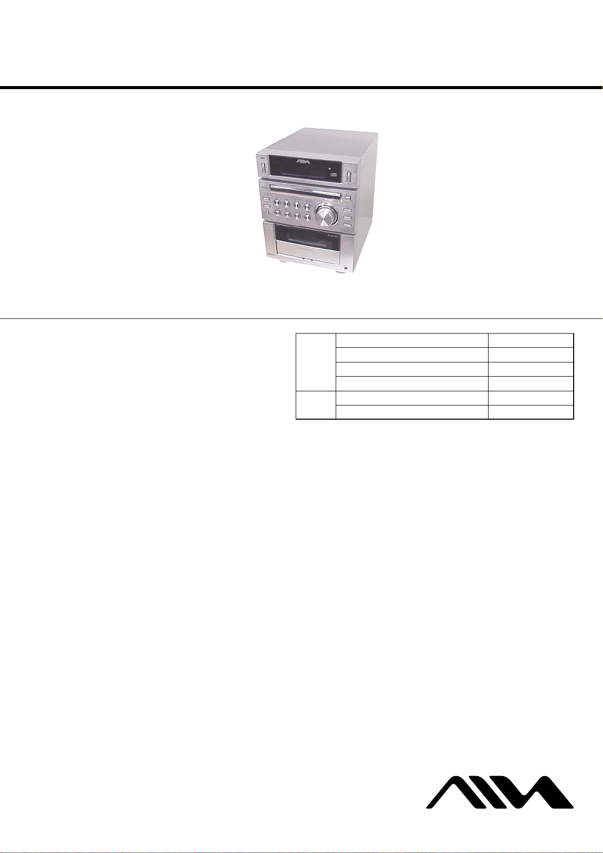
CX-LFA660/LFA770 are the Amplifier , CD pla yer, Tape
Deck and Tuner section in XR-FA660/FA770.
Photo : CX-LFA660
CD CD Mechanism Type CDM77B-F1BD81A
Section Base Unit Name BU-F1BD81A
TAPE Model Name Using Similar Mechanism NEW
Section Tape Transport Mechanism T ype CMAL1Z240A
AEP Model
UK Model
CX-LFA660/LFA770
Australian Model
CX-LFA660
Model Name Using Similar Mechanism NEW
Optical Pick-up Name KSM-215DCP/C2NP
SPECIFICATIONS
Amplifier section
CX-LFA770 for XR-FA770
DIN power output (rated): 55 + 55 W
(6 ohms at 1 kHz, DIN)
Continuous RMS power output (referen ce):
70 + 70 W
(6 ohms at 1 kHz, 10%
THD)
Music power output (reference):
125 + 125 W
CX-LFA660 for XR-FA660
European model:
DIN power output (rated): 40 + 40 W
(6 ohms at 1 kHz, DIN)
Continuous RMS power output (referen ce):
50 + 50 W
(6 ohms at 1 kHz, 10%
THD)
Music power output (reference):
85 + 85 W
Other models:
The following measured at AC 230 – 240 V, 50/60 Hz
DIN power output (rated): 40 + 40 W
(6 ohms at 1 kHz, DIN)
Continuous RMS power output (referen ce):
50 + 50 W
(6 ohms at 1 kHz, 10%
THD)
Inputs
MD IN (RCA pin jacks): Sensitivity 2 V,
impedance 47 kilohms
Outputs
PHONES (stereo mini jack):
Accepts headphones with
an impedance of 32 ohms
or more
SPEAKER: Accepts impedance of
6ohms
CD player section
Laser Semiconductor laser
(λ=770 – 810 nm)
Emission duration:
continuous
Frequency response 20 Hz – 20 kHz
Tape deck section
Recording system 4-track 2-channel, stereo
— Continued on next page —
9-879-045-02
2005J16-1
© 2005.10
COMPACT DISC DECK RECEIVER
Sony Corporation
Personal Audio Division
Published by Sony Engineering Corporation
Page 2

CX-LFA660/LFA770
Frequency response 50 – 13,000 Hz (±3 dB),
using Sony TYPE I
cassettes
Tuner section
FM stereo, FM/AM superheterodyne tuner
FM tuner section
Tuning range 87.5 – 108.0 MHz
(50-kHz step)
Antenna FM lead antenna
Antenna terminals 75 ohms unbalanced
Intermediate frequency 10.7 MHz
AM tuner section
European model: 531 – 1,602 kHz
(with the tuning interval
set at 9 kHz)
Other models: 530 – 1,710 kHz
(with the tuning interval
set at 10 kHz)
531 – 1,602 kHz
(with the tuning interval
set at 9 kHz)
Antenna AM loop antenna, external
antenna terminal
Intermediate frequency 450 kHz
General
Power requirements
European model: 230 V AC, 50/60 Hz
Australian model: 230 – 240 V AC, 50/60 Hz
Power consumption
XR-FA770: 75 W
0.3 W (in Power Saving
Mode)
XR-FA660
European model: 65 W
0.3 W (in Power Saving
Mode)
Other models: 70 W
Dimensions (w/h/d) Approx. 190 × 250 × 308
mm incl. projecting parts
and controls
Mass
CX-LFA770 for XR-FA770:
Approx. 6.1 kg
CX-LFA660 for XR-FA660:
Approx. 5.8 kg
Design and specifications are subject to change
without notice.
TABLE OF CONTENTS
1. SERVICING NOTES ................................................ 3
2. GENERAL ................................................................... 5
3. DISASSEMBLY
3-1. Disassembly Flow ........................................................... 8
3-2. Top Cabinet, Tuner (FM/AM), DC Fan.......................... 9
3-3. Panel (DVD) .................................................................... 9
3-4. CD Mechanism Section................................................... 10
3-5. Front Panel Section ......................................................... 10
3-6. MAIN Board.................................................................... 11
3-7. FRONT Board ................................................................. 11
3-8. Cassette Deck Mechanism............................................... 12
3-9. Power Transformer .......................................................... 12
3-10. Tray (AU) ........................................................................ 13
3-11. MS-128 Board ................................................................. 13
3-12. Base Unit, Belt, Driving Gear ......................................... 14
4. TEST MODE ............................................................... 15
5. MECHANICAL ADJUSTMENTS......................... 16
6. ELECTRICAL ADJUSTMENTS .......................... 17
7. DIAGRAMS
7-1. Block Diagram – BD Section –...................................... 22
– MAIN Section – ........................................................... 23
7-2. Printed Wiring Board – BD81A Section – ..................... 24
7-3. Schematic Diagram – BD81A Section –........................ 25
7-4. Printed Wiring Boards – MAIN Section – ..................... 26
7-5. Schematic Diagram – MAIN Section (1/2) –................. 27
7-6. Schematic Diagram – MAIN Section (2/2) –................. 28
7-7. Printed Wiring Board – FRONT Section –..................... 29
7-8. Schematic Diagram – FRONT Section – ....................... 30
7-9. Printed Wiring Board – AMP Section – ......................... 31
7-10. Schematic Diagram – AMP Section – ............................ 32
7-11. Printed Wiring Board – PT Section – ............................. 33
7-12. Schematic Diagram – PT Section –................................ 33
8. EXPLODED VIEWS
8-1. Overall Section ................................................................ 41
8-2. Front Section ................................................................... 42
8-3. Chassis Section................................................................ 43
8-4. CD Mechanism Deck Section (CDM77B-F1BD81A).... 44
8-5. Base Unit (BU-F1BD81A).............................................. 45
9. ELECTRICAL PARTS LIST .................................. 46
2
Page 3
SECTION 1
SERVICING NOTES
CX-LFA660/LFA770
Notes on chip component replacement
• Never reuse a disconnected chip component.
• Notice that the minus side of a tantalum capacitor may be
damaged by heat.
Flexible Circuit Board Repairing
• Keep the temperature of the soldering iron around 270 °C
during repairing.
• Do not touch the soldering iron on the same conductor of the
circuit board (within 3 times).
• Be careful not to apply force on the conductor when soldering
or unsoldering.
UNLEADED SOLDER
Boards requiring use of unleaded solder are printed with the leadfree mark (LF) indicating the solder contains no lead.
(Caution: Some printed circuit boards may not come printed with
the lead free mark due to their particular size)
: LEAD FREE MARK
Unleaded solder has the following characteristics.
• Unleaded solder melts at a temperature about 40 °C higher
than ordinary solder.
Ordinary soldering irons can be used but the iron tip has to be
applied to the solder joint for a slightly longer time.
Soldering irons using a temperature regulator should be set to
about 350 °C.
Caution: The printed pattern (copper foil) may peel away if
the heated tip is applied for too long, so be careful!
• Strong viscosity
Unleaded solder is more viscou-s (sticky, less prone to flow)
than ordinary solder so use caution not to let solder bridges
occur such as on IC pins, etc.
• Usable with ordinary solder
It is best to use only unleaded solder but unleaded solder may
also be added to ordinary solder.
CAUTION
Use of controls or adjustments or performance of procedures
other than those specified herein may result in hazardous radiation
exposure.
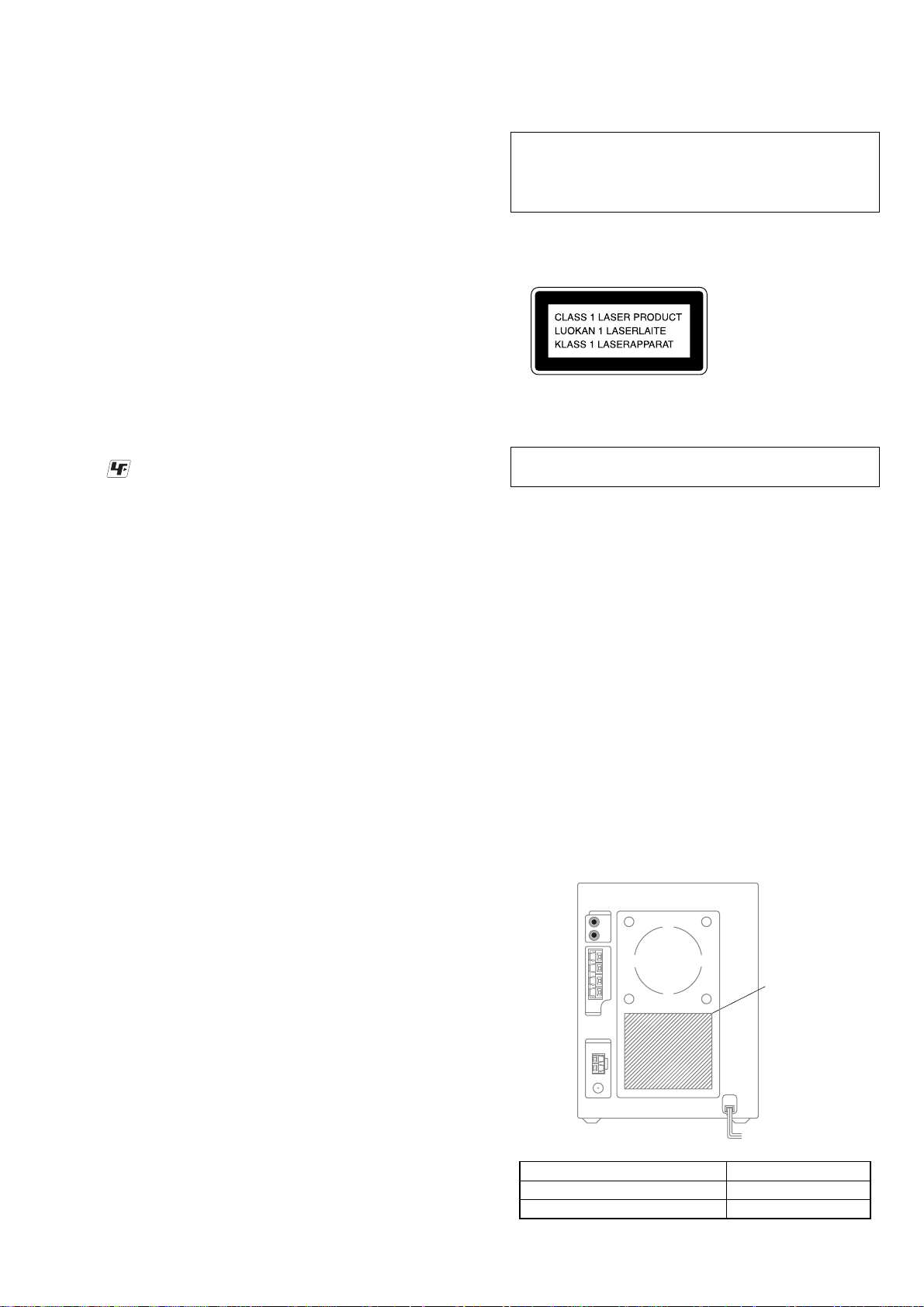
This appliance is classified as a CLASS 1 LASER product.
The CLASS 1 LASER PRODUCT MARKING is located on the
rear exterior.
Laser component in this product is capable of emitting radiation
exceeding the limit for Class 1.
NOTES ON HANDLING THE OPTICAL PICK-UP
BLOCK OR BASE UNIT
The laser diode in the optical pick-up block may suffer electrostatic
break-down because of the potential difference generated by the
charged electrostatic load, etc. on clothing and the human body.
During repair, pay attention to electrostatic break-down and also
use the procedure in the printed matter which is included in the
repair parts.
The flexible board is easily damaged and should be handled with
care.
NOTES ON LASER DIODE EMISSION CHECK
The laser beam on this model is concentrated so as to be focused on
the disc reflective surface by the objective lens in the optical pickup block. Therefore, when checking the laser diode emission,
observe from more than 30 cm away from the objective lens.
LASER DIODE AND FOCUS SEARCH OPERATION
CHECK
Carry out the “S curve check” in “CD section adjustment” and check
that the S curve waveforms is output three times.
SAFETY-RELATED COMPONENT WARNING!!
COMPONENTS IDENTIFIED BY MARK 0 OR DOTTED LINE
WITH MARK 0 ON THE SCHEMATIC DIAGRAMS AND IN
THE PARTS LIST ARE CRITICAL TO SAFE OPERATION.
REPLACE THESE COMPONENTS WITH SONY PARTS WHOSE
PART NUMBERS APPEAR AS SHOWN IN THIS MANUAL OR
IN SUPPLEMENTS PUBLISHED BY SONY.
MODEL IDENTIFICATION
– Back Panel –
Part No.
Model Name Part No.
AEP and UK models 2-067-053-0[ ]
Australian model 2-067-053-2[ ]
3
Page 4
CX-LFA660/LFA770
k
• SERVICE POSITION OF THE CD MECHANISM DECK
*
Lay the CX-LFA660/LFA770 with the left-side facing downward and then check the CD mechanism deck after removing it
from the Holder Mech.
MAIN Board
holder mech
CD mechanism deck
• SERVICE POSITION OF THE TAPE CASSETTE MECHANISM DECK
*
Remove the CD mechanism deck and the Holder mech from the unit and check the tape cassette mechanism deck with
the front panel being open.
front panel
tape cassette mechanism dec
4
Page 5
SECTION 2
Main unit
ALBUM +/– qj (10, 11, 16)
BASS/TRE qa (18)
Cassette compartment qd
CD SYNC wa (16)
Disc tray 6
DISPLAY 8 (14, 21)
Display window 5
i-Bass q; (18)
MD ql (23)
PHONES jack qf
PLAY MODE qs (9, 11, 15, 16,
17)
Remote sensor 7
TUNER/BAND 4 (12, 13)
TUNING +/– qk (12, 13)
TUNING MODE qs (12, 13)
VOLUME control qg (26)
?/1 (power) 1 (7, 13, 26)
TAPE nN (play) 2 (15, 16)
CD NX (play/pause) 3 (9)
Z CD (open/close) 9 (9)
Z PUSH OPEN (tape open/close)
qd (15)
x (stop) qh (10, 12, 15, 16, 26)
m/M (rewind/fast forward)
qk (10, 15)
l/L (go back/go forward)
qk (10, 17, 18)
z REC PAUSE/START (record)
w; (16)
List of button locations and reference pages
How to use this page
Use this page to find the location of buttons and other
parts of the system that are mentioned in the text.
Illustrati
on number
r
DISPLAY
8 (
14, 21
)
RR
Name of button/ pa r t Reference page
ALPHABETICAL ORDER
A – O
P – Z
BUTTON DESCRIPTIONS
1234 567 8
9
q;
qa
qs
qf
qd
qg
qhqjqk
ql
w;
wa
GENERAL
CX-LFA660/LFA770
This section is extracted
from instruction manual.
5
Page 6
CX-LFA660/LFA770
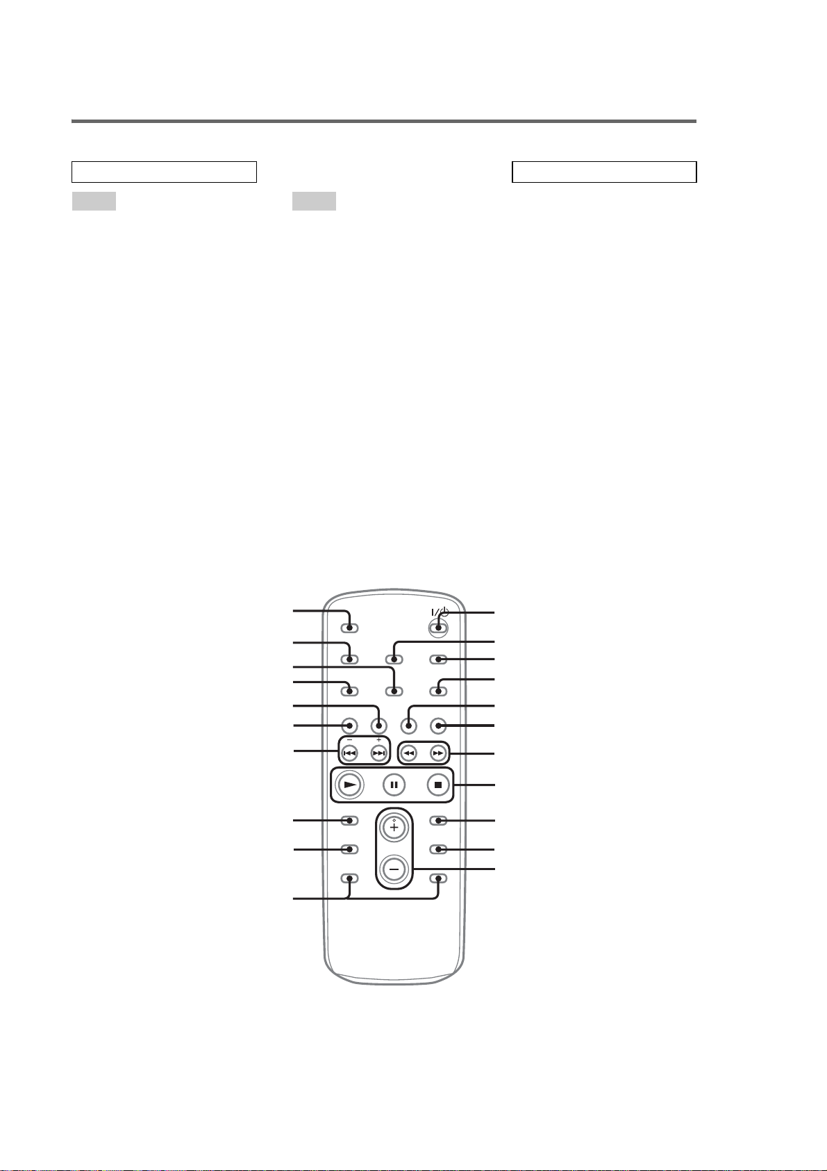
Remote control
ALPHABETICAL ORDER
A – O P – Z
ALBUM +/– qs (10, 11)
CD qj (9, 11)
CLEAR qf (11)
CLOCK/TIMER SELECT 2
(19, 20)
CLOCK/TIMER SET 3 (8, 19,
20)
DISC SKIP* q;
DISPLAY w; (14, 21)
ENTER 9 (8, 11, 12, 19, 20)
EQ qd (18)
FM MODE 4 (14)
FUNCTION 6 (9, 11, 15, 20, 23)
PLAY MODE ql (9, 11, 15, 20)
REPEAT 4 (10)
SLEEP wa (18)
TAPE qh (15, 20)
TUNER BAND 5 (12, 13)
TUNER MEMORY qk (12)
TUNING MODE ql (12, 13)
VOLUME +/– qa (19)
BUTTON DESCRIPTIONS
?/1 (power) 1 (7, 19)
m/M (rewind/fast forward )
7 (10, 15)
x (stop) 8 (10, 12, 15)
X (pause) 8 (10, 15)
N (play) 8 (9, 15, 20)
./> (go back/go forward)
qg (8, 10, 18, 19)
+/– (tuning) qg (12)
*Button does not function with
this model.
wa
w;
ql
qk
qj
qh
qg
qf
qd
qs
1
2
3
4
5
6
7
8
9
0
qa
6
Page 7

Setting the clock
Use buttons on th e remote for the operatio n.
1
Press ?/1 to turn on the system.
2
Press CLOCK/TIMER SET.
3
Press . or > rep eatedly to set the
hour.
4
Press ENTER.
5
Press . or > rep eatedly to set the
minute.
6
Press ENTER.
The clock sta rt s working.
To adjust the clock
CX-LFA660/LFA770
1
Press CLOCK/T IM ER SE T.
2
Press . or > repeatedly until “CLOCK”
appears, then press ENTER.
3
Do the same procedures as step 3 to 6
above.
7
Page 8
CX-LFA660/LFA770
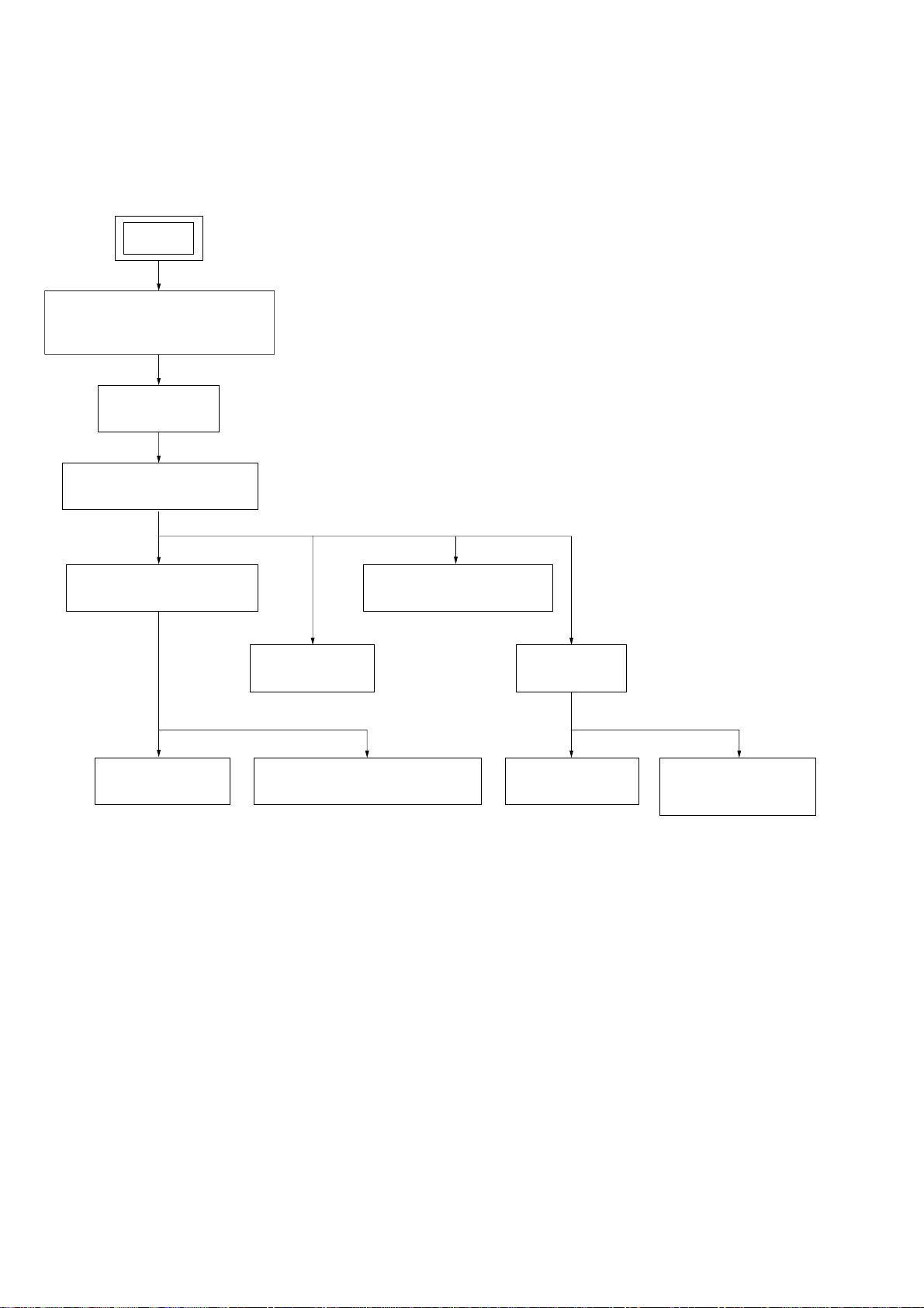
3-1. DISASSEMBLY FLOW
•This set can be disassembled in the order shown below.
SET
SECTION 3
DISASSEMBLY
3-2. T OP CABINET , TUNER (FM/AM),
DC FAN
(Page 9)
3-3. PANEL (DVD)
(Page 9)
3-4. CD MECHANISM SECTION
(Page 10)
3-5. FRONT PANEL SECTION
(Page 10)
3-6. MAIN BOARD
(Page 11)
3-9. POWER TRANSFORMER
(Page 12)
3-10. TRAY (AU)
(Page 13)
3-7. FRONT BOARD
(Page 11)
3-8. CASSETTE DECK MECHANISM
(Page 12)
3-11. MS-128 BOARD
(Page 13)
3-12. BASE UNIT, BELT,
DRIVING GEAR
(Page 14)
8
Page 9
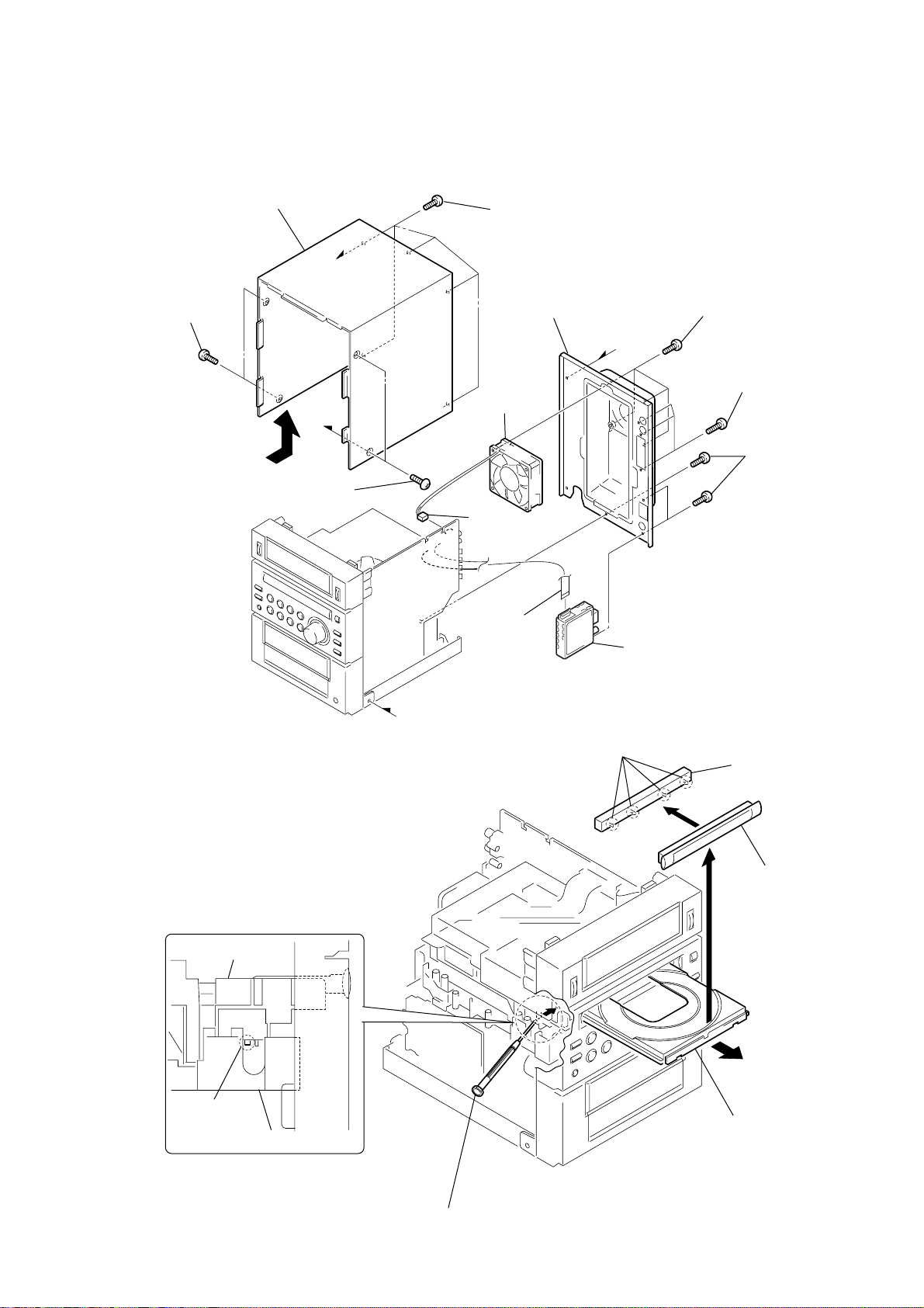
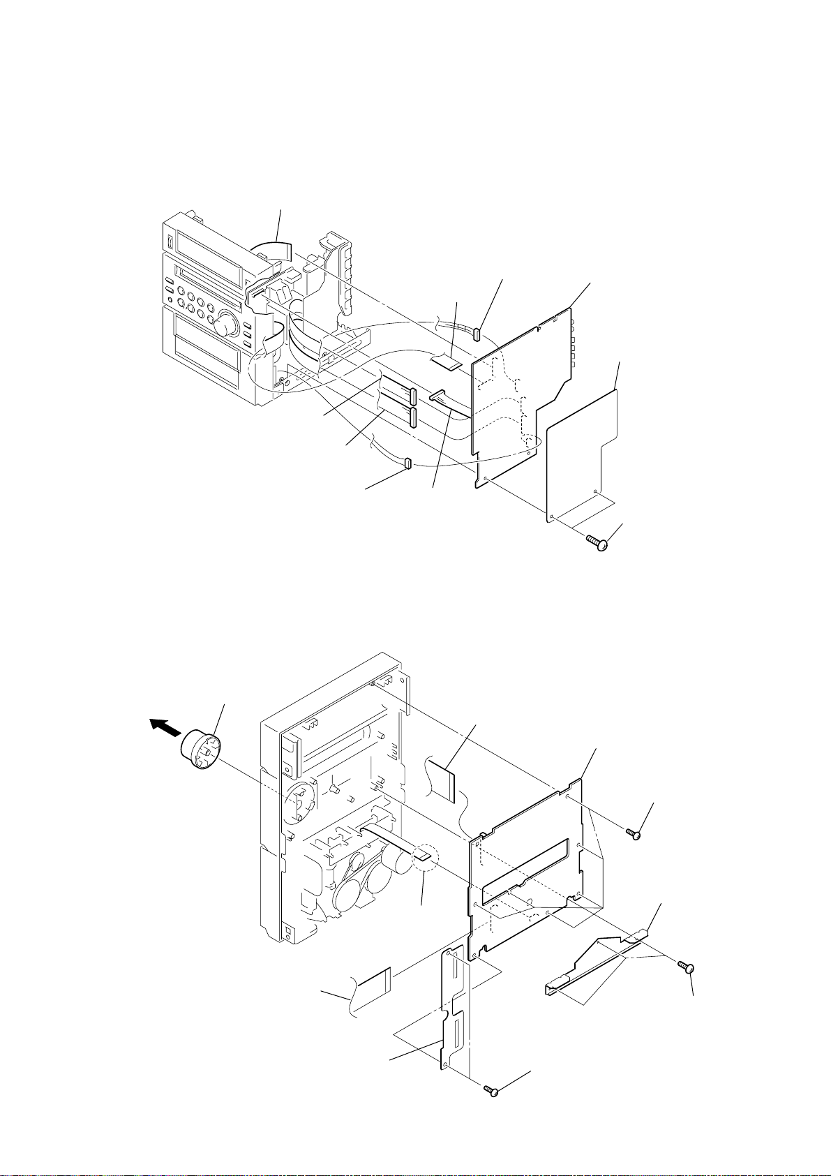
Note: Follow the disassembly procedure in the numerical order given.
3-2. TOP CABINET, TUNER (FM/AM), DC FAN
5
2
two s
(+BVTP 3
crews
×
8)
top cabinet
b
4
1
two s
(+BVTP 3
crews
a
×
8)
3
five s
qd
DC fan
crews
rear panel
(+BVTP 3
qs
q;
connector
(3P)(CN290)
CX-LFA660/LFA770
×
8)
qa
four s
(+BVTP 3
a
crews
×
8)
6
three s
(+BVTP 3
7
(+BVTP 3
crews
three s
×
10)
crews
×
8)
3-3. PANEL (DVD)
CD mechanism
8
wire (flat type)
(15 core)
b
3
four claws
9
tuner
4
base loading
5
panel (DVD)
chuck cam
2
holder mecha
1
Move the chuck cam located at the bottom of the CD mechanism in the direction of the arrow
using the flathead screwdriver.
Pull-out the disc tray.
9
Page 10
CX-LFA660/LFA770
)
3-4. CD MECHANISM SECTION
6
CD mechanism deck
(CDM77B-F1BD81A)
8
two s
(+BVTP 3
3
three s
(+BVTP 3
5
wire (flat type) (5 core)
crews
×
crews
8)
1
two s
(+BVTP 2.6
2
shield case (mecha)
×
10)
4
wire (flat type)
(27 core)
9
two s
(+BVTP 3
crews
crews
×
10)
×
8)
q;
holder mecha
3-5. FRONT PANEL SECTION
2
1
screw
(+B 3)
earth wire
5
wire (flat type)
(25core) (CN603)
9
connector
(7P) (CN601)
qd
claw
7
s
crew
(+BVTP 3
×
10
10
qa
two screws
(+KTP 3
qf
front panel section
7
×
8)
screw
(+KTP 3
4
earth wire
3
screw
qs
claw
8
connector
6
wire (flat type)
(21core) (CN602)
×
8)
q;
two screws
(+KTP 3
×
8)
(5P) (CN201)
(+B 3)
Page 11
3-6. MAIN BOARD
)
2
wire (flat type)
(25core) (CN603)
7
connector
(9P) (CN002)
8
connector
(11P) (CN003)
3
wire (flat type)
(21core) (CN602)
5
connector
(7P) (CN601)
CX-LFA660/LFA770
q;
MAIN board
9
sheet (PWB MAIN)
3-7. FRONT BOARD
1
knob (VOL)
6
connector
(5P) (CN201)
1
connector
(10P) (CN257)
8
w
ire (flat type)
25core (CN802)
q;
FRONT board
4
two s
six s
crews
crews
3
bracket
(+BVTP 3
4
(+BVTP 2.6
×
10)
×
10)
9
w
ire (flat type)
21core (CN801)
6
sheet (protection)
7
w
ire (flat type)
8core (CN803)
5
two s
(+BVTP 2.6
crews
2
three s
crews
×
(+BVTP 3
×
10)
10
11
Page 12
CX-LFA660/LFA770
)
3-8. CASSETTE DECK MECHANISM
3
cassette deck mechanism
1
four screws
(+BVTP 3
×
10)
3-9. PO WER TRANSFORMER
5
binding band
9
Remove the soldering.
q;
PT board
1
s
(+B 3)
2
earth wire
crew
4
binding band
6
connector
(CN202)
2
earth wire
3
four s
crews
7
(+BVTP 3
8
holder (PWB PT
qa
power transformer
s
crew
×
8)
12
Page 13
3-10. TRAY (AU)
2
1
Move the Chuck cam in the direction of the arrow.
bottom side
two claws
3
CX-LFA660/LFA770
3-11. MS-128 BOARD
1
belt
4
5
tray (AU)
2
wire (flat type)
(5core) (CN001)
4
MS-128 board
3
four claws
13
Page 14
CX-LFA660/LFA770
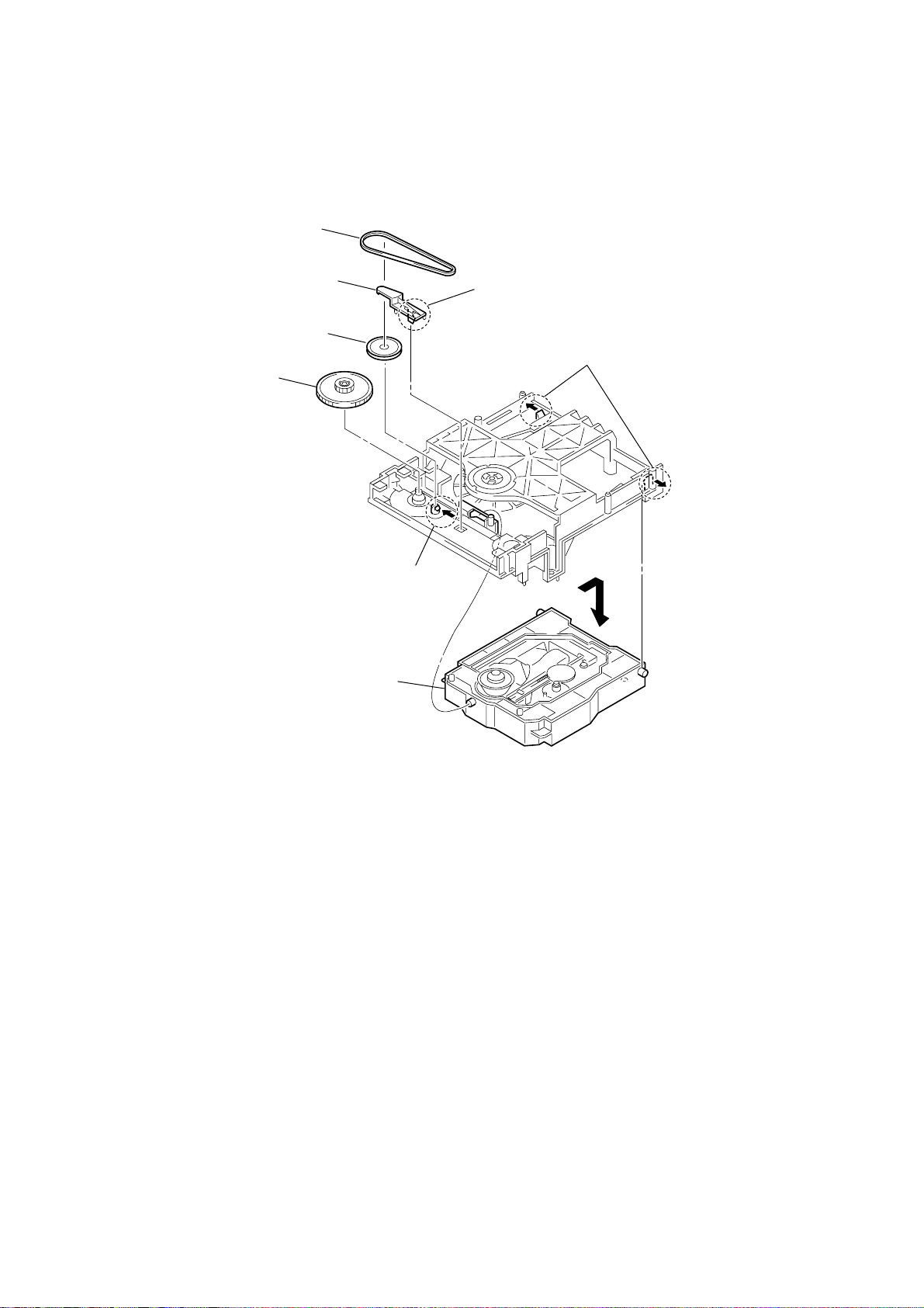
3-12. BASE UNIT, BELT, DRIVING GEAR
4
belt
6
support
8
pulley gear
9
driving gear
5
claw
1
two claws
3
base unit
(BU-F1BD81A)
7
claw
2
14
Page 15
SECTION 4
TEST MODE
CX-LFA660/LFA770
Note 1: Regarding the notification symbol “R”
Because the number of the operating buttons of this product
are limited, some operations require use of the operating
buttons of the remote commander. When a specific operation
requires use of the operating buttons of the remote commander,
“R” is added to the specific operating procedure in this manual.
Example MENU/NO “R” The MENU/NO button of remote
commander.
Note 2: Incorrect operations may be performed if the test mode is
not entered properly.
In this case, press the ?/1 button to turn the po wer of f, and
retry to enter the test mode.
1. Cold Reset
• The cold reset clears all data including preset data stored in
the RAM to initial conditions. Execute this mode when
returning the set to the customers.
Procedure:
1. Press three buttons x , [VOLUME] (down) and ?/1
simultaneously.
2. When this button is operated, all of the settings are reset.
2. Panel Test Mode
•This mode is used to check the software version, LCD, LED
and keyboard.
Procedure:
1. Press three bottons [DISPLAY], ?/1 and [VOLUME] (down)
simultaneously.
2. When the panel test mode is activated, all se gments are turned
on.
4. Repeat 5 Times Limit Release Mode
Procedure:
1. Press the ?/1 button to turn the power on.
2.
Press three buttons
simultaneously.
3. To exit from this mode, press the ?/1 button.
5. Disc Tray Lock
The disc tray lock function for the antitheft of an demonstration
disc in the store is equipped.
Setting Procedure :
1. Press the ?/1 button to turn the set on.
2. Insert a disc.
3. Press the x button and the Z CD button simultaneously for
five seconds.
4. The message “LOCKED” is displayed and the tray is locked.
Releasing Procedure :
1.
Press the
five seconds again.
2. The message “UNLOCKED” is displayed and the tray is
unlocked.
Note: When “LOCKED” is displayed, the slot lock is not released by
turning power on/off with the ?/1 button.
x , [VOLUME] (down)
x
button and the Z CD button simultaneously
and the [PLAY MODE]
for
2-1. V ersion T est Mode
Procedure:
1. When the panal test mode is activated, press the [BASS/
TREBLE] button and the version is displayed.
2. Press the [i-Bass] button and the date of the software production
is displayed.
3. Press the [BASS/TREBLE] button again and the version is
displayed.
4. To exit from this mode, pull out the AC plug.
2-2. Key Test Mode
Procedure:
1. When the panel test mode is activated, press the [PLAY MODE]
button, to select the key test mode. In the ke y check mode, the
fluorecent indicator displays “KEY 0”. Each time a button is
pressed, “KEY” value increases. However, once a button is
pressed, it is no longer taken into account. When all keys are
pressed correctly, “KEY 19” is displayed.
2. To exit from this mode, pull out the AC plug.
3. Common Test
Procedure:
1. Press the ?/1 button to turn the power on.
2. When the common test mode is activated, each time press the
EQ “R” button, the message “EQ MAX”, “EQ MIN”, “EQ
FLAT” is displayed in this order.
3. The message “Volume MAX” is displayed, when press the
[VOLUME] (up) button or V OLUME + “R” b utton. The message “Volume MIN” is displayed, when press the [VOLUME]
(down) button or VOLUME – “R” button.
4. To exit from this mode, press the ?/1 button to turn off the
main power.
15
Page 16

CX-LFA660/LFA770
SECTION 5
MECHANICAL ADJUSTMENTS
Precaution
1. Clean the following parts with a denatured alcohol-moistened
swab:
record/playback heads pinch rollers
erase head rubber belts
capstan idlers
2. Demagnetize the record/playback head with a head demagnetizer.
3. Do not use a magnetized screwdriver for the adjustments.
4. After the adjustments, apply suitable locking compound to
the parts adjusted.
5. The adjustments should be performed with the rated power
supply voltage unless otherwise noted.
Torque Measurement
Mode
FWD
FWD
back tension
REV
REV
back tension
FF/REW
FWD tension
REV tension
Torque meter Meter reading
2.94 – 7.84 mN • m
CQ-102C
CQ-102C
CQ-102RC
CQ-102RC
CQ-201B
CQ-403A
CQ-403R
(30 to 79 g • cm)
(0.42 – 1.11 oz • inch)
0.15 – 0.59 mN • m
(2 to 6 g • cm)
(0.03 – 0.08 oz • inch)
2.94 – 7.84 mN • m
(30 to 79 g • cm)
(0.42 – 1.11 oz • inch)
0.15 – 0.59 mN • m
(2 to 6 g • cm)
(0.03 – 0.08 oz • inch)
6.86 – 17.64 mN • m
(70 to 179 g • cm)
(0.98 – 2.49 oz • inch)
9.8 mN • m or more
(100 g • cm or more)
(1.4 oz • inch or more)
9.8 mN • m or more
(100 g • cm or more)
(1.4 oz • inch or more)
16
Page 17
SECTION 6
ELECTRICAL ADJUSTMENTS
CX-LFA660/LFA770
DECK SECTION 0 dB=0.775V
1. Demagnetize the record/playback head with a head
demagnetizer.
2. Do not use a magnetized screwdriver for the adjustments.
3. After the adjustments, apply suitable locking compound to
the parts adjusted.
4. The adjustments should be performed with the rated power
supply voltage unless otherwise noted.
5. The adjustments should be performed in the order given in
this service manual. (As a general rule, playback circuit
adjustment should be completed before performing recording
circuit adjustment.)
6. The adjustments should be performed for both L-CH and RCH.
7. Switches and controls should be set as follows unless otherwise
specified.
Signal Used forTape
P-4-A100
WS-48B
[Record/Playback Head Azimuth Adjustment]
Procedure:
1. Mode : Playback
test tape
P-4-A100
(10kHz, –10dB)
10 kHz, –10 dB
3 kHz, 0 dB
MAIN board
J201
speaker terminal
Azimuth Adjustment
Tape Speed Adjustment
level meter
3. Mode: Playback
test tape
P-4-A100
(10kHz, –10dB)
set
in phase 45
MAIN board
J201
speaker terminal
L
R
Waveform of oscilloscope
°
90
°
good
135
oscilloscope
°
wrong
180
°
4. After the adjustments, apply suitable locking compound to
the parts adjusted.
Adjustment Location: Record/Playback/Erase Head
set
+
–
2. Turn the adjustment screw and check output peaks. If the peaks
do not match for L-CH and R-CH, turn the adjustment screw
so that outputs match within 1 dB of peak.
L-CH
peak
screw
position
R-CH
peak
output
level
within
1 dB
L-CH
peak
R-CH
peak
within 1dB
screw
position
adjustment screw
[Tape Speed Check]
Procedure:
1. Turn the power on.
2. Insert the WS-48B into deck.
3. Press the TAPE nN button of deck.
4. Check the reading of frequency counter becomes 3000 ± 90
Hz.
Sample Value of Wow and flutter
W.RMS (JIS) less than 0.3%
(test tape: WS-48B)
17
Page 18
CX-LFA660/LFA770
CD SECTION
Note:
1. Use YEDS-18 disc (3-702-101-01) unless otherwise indicated.
2. Use an oscilloscope with more than 10MΩ impedance.
3. Clean the object lens by an applicator with neutral detergent when the
signal level is low than specified value with the following checks.
S-curve Check
Connection:
oscilloscope
BD81A board
TP (FEO)
TP (VC)
Procedure:
1. Connect an oscilloscope to test point TP (FEO) and TP (VC)
on the BD81A board.
2. Turn the power on.
3. Put the disc (YEDS-18) in and press the button
and actuate the focus search. (actuate the focus search when
disc table is moving in and out)
4. Check the oscilloscope waveform (S-curve) is symmetrical
between A and B. And confirm peak to peak level within 2 ± 1
Vp-p.
S-curve waveform
+
–
symmetry
A
B
CD
NX
within 2
±
1 Vp-p
RFDC signal waveform
VOLT/DIV: 200 mV
TIME/DIV: 500 ns
±
level: 0.6
0.15 Vp-p
Checking Location: BD81A board (Side B)
RFAC Level Check
Connection:
oscilloscope
BD81A board
TP (RFACO)
TP (VC)
+
–
Procedure:
1. Connect an oscilloscope to test point TP (RF ACO) and TP
(VC) on the BD81A board.
2. Turn the power on.
3. Put the disc (YEDS-18) in to playback the number five track.
4. Confirm that oscilloscope waveform is clear and check RFAC
signal level is correct or not.
Note:
A clear RFAC signal waveform means that the shape “◊” can be
clearly distinguished at the center of the waveform.
RFAC signal waveform
VOLT/DIV: 200 mV
TIME/DIV: 500 ns
Note:
•Try to measure several times to make sure than the ratio of A : B
or B : A is more than 10 : 7.
•Take sweep time as long as possible and light up the
brightness to obtain best waveform.
Checking Location: BD81A board (Side B)
RFDC Le
vel Check
Connection:
oscilloscope
BD81A board
TP (RFDCO)
TP (VC)
+
–
Procedure:
1. Connect an oscilloscope to test point (RFDCO) and TP (VC)
on the BD81A board.
2. Turn the power on.
3. Put the disc (YEDS-18) in to playback the number five track.
4. Confirm that oscilloscope wav eform is clear and check RFDC
signal level is correct or not.
A clear RFDC signal waveform means that the shape “◊” can be
Note:
clearly distinguished at the center of the waveform.
Checking Location: BD81A board (Side B)
level: 1.0
±
0.4 Vp-p
18
Page 19

CX-LFA660/LFA770
E-F Balance Adjustment
Connection:
oscilloscope
BD81A board
TP (TEO)
TP (VC)
+
–
Procedure:
1. Connect an oscilloscpe to test point TP (TEO) and TP (VC) on
the BD81A board.
,,
PLAY MODE/TUNING MODE
2. Press three buttons
and simulfaneously enter the CD test mode.
Z
CD
x
3. Put the disc (YEDS-18) in to playback the number five track.
CD
4. Press the button. If it plays, press theCD
NX
NX
button again. (The tracking servo and the sledding servo are
turned OFF)
5. Check the level B of the oscilliscope's waveform and the A
(DC voltage) of the center of the Traverse waveform.
Confirm the following :
A/B x 100 = less than ± 10%
Traverse Wavef orm
0V
Center of
the waveform
B
A (DC
voltage)
level: 1.0 ± 0.5 Vp-p
Checking Location:
– BD81A BOARD (Side B) –
BD81A BOARD
(SideB)
IC251
TP
(VC)
TP
(TEO)
TP
(FEO)
TP
(RFDCO)
IC303
IC301
IC101
TP
(RFACO)
6. Press the button. (The tracking servo and
CD
NX
sledding servo are turned ON)
7. To exit from this mode, turn the power off.
Notes: •Always move the optical pick-up to most inside track when
0V
exiting from this mode. Otherwise, a disc will not be unloaded.
• Do not run the sled motor excessively, otherwise the gear can
be chipped.
Traverse Wavef orm
Tracking servo
Sled servo
OFF
Tracking servo
Sled servo
ON
C (DC
voltage)
Checking Location: BD81A board (Side B)
19
Page 20

CX-LFA660/LFA770
MEMO
20
Page 21

SECTION 7
D
DIAGRAMS
CX-LFA660/LFA770
• Circuit Boards Location
FRONT BOARD
PT BOARD
HP BOARD
BD81A BOARD
MAIN BOARD
THIS NOTE IS COMMON FOR PRINTED WIRING BOARDS AND SCHEMATIC DIAGRAMS.
(In addition to this, the necessary note is printed in each block.)
For Schematic Diagrams.
Note:
• All capacitors are in µF unless otherwise noted. (p: pF)
50 WV or less are not indicated except f or electrolytics and
tantalums.
• All resistors are in Ω and 1/
specified.
• f : internal component.
• C : panel designation.
Note: The components identified by mark 0 or dotted
line with mark 0 are critical for safety.
Replace only with part number specified.
• A : B+ Line.
• B : B– Line.
•Voltages and waveforms are dc with respect to ground
under no-signal (detuned) conditions.
No mark: FM
( ) : CD STOP
•Voltages are taken with a VOM (Input impedance 10 MΩ).
Voltage v ariations ma y be noted due to normal production
tolerances.
•Waveforms are taken with a oscilloscope.
Voltage v ariations ma y be noted due to normal production
tolerances.
• Circled numbers refer to waveforms.
• Signal path.
F : TUNER
J : CD
d : AUX
E : PB (TAPE)
a : REC (TAPE)
4
W or less unless otherwise
For Printed Wiring Boards.
Note:
• X : parts extracted from the component side.
• Y : parts extracted from the conductor side.
• f : internal component.
• : Pattern from the side which enables seeing.
• Indication of transistor.
C
Q
B
E
B
•Abbreviation
AUS: Australian model
These are omitted.
CE
These are omitted.
MS-128 BOARD
AMP BOAR
CX-LFA660/LFA770
2121
Page 22

CX-LFA660/LFA770
7-1. BLOCK DIAGRAM — BD SECTION —
OPTICAL PICK-UP
BLOCK
(KSM-215DCP/C2NP)
DETECTOR
VCC
VC
FOCUS
COIL
TRACKING
COIL
M101
(SPINDLE)
M102
(SLED)
IC301
+1.7V
+3.3V
A
B
C
D
E
F
Q10
VR
LD
GND
PD
F
F+
T+
T
M
M
16
15
17
18
19
20
21
22
LD
DRIVER
IC251
SL/SP MOTOR
DRIVER
CH2OUT-F
CH1FIN
CH2OUT-R
CH1RIN
CH1OUT-R
CH2FIN
CH1OUT-F
CH2RIN
CH4OUT-F
CH4OUT-R
CH3OUT-R
CH3OUT-F
SFDR
SRDR
OPIN+
MUTE
X171
16.9MHz
+3.3V
SW101
5
6
7
8
9
10
3
24
26
27
28
29
19
20
36
77
78
37
7
11
12
13
14
30
29
6
100
A
B
C
D
E
F
LD
XTAO
XTAI
PD
SSTP
TFDR
TRDR
FFDR
FRDR
CH3FIN
CH3RIN
MPD
XRST
IC101
RF AMP
PCMD1
LRCK1
LRCK
PCMD
BCK
BCK1
XTACN
XRST
DATA
XLAT
CLOCK
SENS
SCOR
GFS
C2PO
FOK
AOUT1
AOUT2
DOUT
61
62
63
65
66
60
95
100
102
104
105
107
115
113
114
1
2
3
81
86
71
XTACN
XRST
DATA
XLAT
CLOCK
SENS
SCOR
DIGITAL SIGNAL
11
SDO0
16
LRCKIA
19
SFSY/LRCK1B
14
SDIO
15
BCKIA
18
SBSY/BCK1B
PROCESSOR
STANBY
PO11/BUCK/AD1
SRMSTB
VDD
VDD
VDDM
MIACK
MICK
MIDIO
MILP
MICS
RESET
55
21
40
36
41
IC303
5 1
REG
3.3V
CN201
3
8
7
6
5
4
2
SCOR
SENS
CLOCK
XLT
DATA
XRST
XTACN
• Signal Path
MP3STB
MP3REQ
MIACK
MICK
MIDIO
MILP
MICS
MP3RST
SRMSTB
SCOR
SENS
CLOCK
XLT
DATA
XRST
XTACN
LOUT
ROUT
DOUT
: CD
A
B
MAIN
SECTION
MAIN
SECTION
CX-LFA660/LFA770
2222
Page 23

— MAIN SECTION —
L
MD
R
TUNER UNIT
DECK
L-CH
REC/PB
HEAD
R-CH
ERASE
HEAD
MECHA BLOCK
SW1
PLAY
SW2
R REC
SW3
F REC
SW4
PACK
+SOL
SW5
PEND
M1
DECK
MOTOR
J601
+10V
L-CH
R-CH
TU-DO
TU-DI
TU-CL
TU-CE
TUNED
STEREO
TU-MUTE
FM SOUT
RDS DATA
RDS INT
M
VCC
R-CH
R-CH
R-CH
R-CH
T301
REC BIAS
Q452,453
Q454
Q804,805
SOL
DRIVE
Q806,807
MOTOR
DRIVE
BIAS
OSC
Q450
Q451
Q306
PB
SWITCH
Q301,302,305
REC
SWITCH
+VM
PB/REC EQ AMP
IC601
OUT L
AUX L
19 18
23
2
21
TU L
TAPE L
CD L
OUT R
CONT
REC OUT
CX-LFA660/LFA770
Q101,103,105
Q107,109
Q111,113,127
PRE
R-CH
16
13
28
SYSTEM CONTROLLER
IC801
O- MUTE
SEG1
SEG16
G1
G12
KEY1
KEY0
VOL ENC
RESET
I-RMC
86
43
45
.
47
50
.
52
60
31
42
20
27
22
87
11
23
29
18
FIL1 FIL2-VFL
S801-808
FUCTION
KEY
S809-815.S817,818
FUCTION
KEY
S616
VOLUME
ENCODER
D802
STAND BY
Q803
RESET
SWITCH
X801
32.768kHz
X802
10MHz
28
FUNC-DATA
75
TU-DI
76
TU-DO
74
TU-CLOCK
73
TU-CE
71
TU TUNED
70
TU STELEO
77
TU MUTE
23
RDS SIG
25
RDS DATA
26
RDS CLK
79
TA-R/P
12
XT1
13
XT2
15
X IN
16
X OUT
80
TA-BIAS
68
TA-PLAY SW
24
TA-SW
TA SOL
81
67
TA-END SW
78
TA-MOTOR
STAND-BY LED
I-POWER-DOWN
I-POWER-MONITOR
FL801
FLUORESCENT
DISPLAY
IC803
RESET
1
IC802
REMOTE
CONTROL
RECEIVER
VDD1
MUTE
Q121
31
AMP
Q280-282
THR DET
D807
D806
2
Q809
+3.3V
REG
VDD2
Q117,119
POWER
AMP
+3.9V
D808
Q123,250,251
OVER
CURRENT
DET
R-CH
R-CH
L
R
Q204,206
DC
DET
Q203,205
DC
DET
L
R
R-CH
Q290-293
FAN
DRIVE
-VH
-VP
+VP
FAN
+VH
J702
HEADPHONES
J201
SPEAKER
Q060-065
DC
DET
-VH
Q201
DET
Q202
DET
-VL
+VL
• R-CH is omitted due to same as L-CH.
• Signal Path
: TUNER
: CD
: AUX
: PB (TAPE)
: REC (TAPE)
POWER
TRANSFORMER(MAIN)
D001
+VH
-VH
VF
VF
D002
PT252
CX-LFA660/LFA770
B
BD SECTION
CD OPEN/CLOSE
TRY
MOTOR
OPEN
CLOSE
AOUT1
AOUT2
M
R-CH
MOTOR DRIVE
IC501
FIN
OUT1
4 7
RIN
OUT2
2 9
BD
SECTION
Q009.010
-VFL
REG
IC001
+7V
3
1
REG
VM
Q001-003
FL
REG
+3.9V
Q006,011,012
REG
Q810-812
+3.9V
REG
VL
D251-254
Q008
RELAY
DRIVE
D256
RY251
PT251
POWER
TRANSFORMER(SUB)
D257
AC
IN
+3.3V
REG
Q020,021
VCC
CD-VCC
IC002
+3.3V
REG
CN701
SCOR
XTCN
XRST
XL-T-CD
CD-DATA
SENS
CD-CLK
A
MP3-DO
MP3-DI
MP3-CLK
MP3-CS
MP3-CP
MP3-ACK
MP3-REQ
MP3-RESET
MP3-STB
C1
C2
C3
C4
C5
C6
C7
C8
C9
C10
C11
C12
C13
C14
C15
C16
C16
C15
C14
C13
C12
C11
C10
C9
C8
C7
C6
C5
C4
C3
C2
C1
6
MP3-STB
2
MP3-RST
3
MP3-REC
1
MI-ACK
O-MI-LP
5
O-MI-CS
4
MI
100
MI-DIO-O
98
MI-DIO-I
99
97
O-CD-CLK
O-CD-SENS
96
O-CD-DATA
95
O-CD-XLT
9
O-CD-XRST
8
O-CD-XTCN
7
I-CD-SCOR
10
91
O-TRY-OPN
92
O-TRY-CLS
65
I-SW-TROPN
I-SW-TRCLS
66
POWER ON
DVDD
AVDD
MP3VD
94CD POWER
85
2323
Page 24

CX-LFA660/LFA770
7-2. PRINTED WIRING BOARD — BD81A SECTION —
12
A
B
C
• See page 21 for Circuit Boards Location. :Uses unleaded solder.
3456789
SPINDLE
MOTOR
IC303
1
3
5
4
(LIMIT)
36
1
IC251
9
192728
IC301
16
17
10
18
32
33
1
64
49
48
SLED
MOTOR
D
E
TP
(VC)
TP
(TEO)
MAIN
12
12
E
OPTICAL
PICK-UP
BLOCK
(KSM–215DCP)
TP
(FEO)
TP
(RFDCO)
(RFACO)
IC101
12
12
TP
BOARD
CN604
(Page 26)
• Semiconductor
Location
Ref. No.
IC101 D-7
IC251 C-6
IC301 C-7
IC303 B-7
Location
CX-LFA660/LFA770
Q10 E-4
2424
Page 25

CX-LFA660/LFA770
7-3. SCHEMATIC DIAGRAM — BD81A SECTION —
R307
10k
TP433
MP3VDD
FB301
MAIN
BOARD
(1/2)
CN604
(Page 27)
C308
C309
0.1 F
C307
0.1 F
47
4V
R303
100k
C310
0.1 F
IC303
BH15FB1W
C302
C303
0.1
0.1
F
F
TP422
MP3GND
CN201
27P
C311
0.1 F
TP401
TP402
TP403
TP404
TP405
TP406
TP407
TP408
TP417
TP416
TP415
TP414
TP413
TP412
TP419
TP410
TP411
TP409
TP434
IC301
TC94A34FG-002
C305
TP186
MVDD
TP187
MGND
MP3STB
MP3REQ
MIACK
MICK
MIDIO
MILP
MICS
MP3RST
R205
SCOR
SENS
CLK
XLT
DATA
XRST
XTCN
AVDD
ROUT
LOUT
DOUT
R204
0
TP304
C316
0.0022 B
TP
301
C315
0
306
R
C312
0.1 F
220
4V
0
R411
R410
R409
R408
R407
R406
R412
C213
22p CH
R313
0.1 B
220
100
100
100
100
100
100
100
22p CH
C212
DVDD
TP435
220p CH
C211
• Refer to page 36 for IC Pin Function Description. • See page 34, 35 for IC Block Diagrams. • See page 34 for Waveforms.
B
C134
0.1 F
42
C1
.0015
C151
100
10V
0
5
16
R
0.1 B
1
15
R
C143
0.1 F
2
14
TP
0
C210
R203
0
TP302
TP303
R351
100
10k
R405
R404
R419
R403
R402
R401
R301
C317
0.01 B
0.1 F
47 4V
C306
0.1 F
100
100
100
100
100
100
C318
0.01
B
100k
R305
100k
C320
0
C174
0.1 F
TP436
AVDD
C201
100
0
10V
R201
TP420
AGND
C203
100
10V
B
09
2
C
.01
0
TP421
DGND
TP427
PCMDI
TP103
LRCK
R352
100
R353
100
TP104
PCMD
R354
100
TP105
C162
R182
100
470p CH
C181
0.1 F
BCK
R161
100
0.1 F
R171C171
47022p CH
R172
1M
16.9MHz27p CH
X171C172
CH
22 6.3V
C183
22 6.3V
C184
0.1 F
C182
C194
0.1
F
C161
0.1 F
0
R173
470p
C185
R181
100
C186
R302
C313
C314
0
k
143
3.3
R
B
141
C
0.1
42
k
1
1
R
.7k
4
41
1
R
O
CK
S
148
EX
SB
TP
49
P1
T
C163
0.1
3
0
16
10
R
R162
47k
B
1
0.0
33
C1
133
80k
1
R
32
0k
1
1
R
IC101
CXD3059AR
0.1
196
C
B
7
C132
0.4
CH
4
I
C12
100p
1M
FAC
R
131
131
R
C
TP125
0
191
R
C125
0.1 F
H
C
B
O
C
30p
15k
0.1
3
FA
R
24
1
TP
4
GF
FCK
145
XU
W
TP14
TP
22
B
0.1
C1
121
R
C123
K
3
47
C
1
XP
P15
TP
T
2
12
P
TP123
T
O
C
FD
R
TP121
R111
1k
C111
0.0033 B
R112
15k
C112
470p
C113
JPO102
JPO103
C115
0.1 F
TP167
LOCK
TP178
FOK
TP166
DFCT
TP165
MIRR
O
FS
2P
P146
G
C
T
T
CK
62
U
D
160
O
P1
P
C
W
T
T
R193
NM
0.0033
FEI
R114
15k
R113
1k
TEI
C114
470p B
0.1 F
C195
+
W
425
S
TP
S101
SW
W
426
S
TP
C11
C10
C15
C14
10
10
0.1
0.1
6.3
6.3
F
F
B
B
TP423
IOP1
C16
R11
0
JPO004
0.0068
R13
1
1
F
TP424
IOP2
R10
3.3
Q10
2SB1690K
C18
0.001 B
TP428
FRDR
TP430
TRDR
MDP
C251
B
R253
10k
IC251
BA5947FM
(HSOP28)
C252
0.1 F
C255
0.1 F
C259
0.1
C258
F
0.1
+
SL+
SP
SL-
2
3
251
25
TP25
TP
TP
F
257
C
0.1
C17
R12
220
100k
4V
JPO10
APC
C116
100
10V
TP177
VC
TP429
FFDR
TP431
TFDR
TP432
MDP
R252
R251
22k
10k
C260
220 10V
CN101
16P
E
TP10
D
TP11
A
TP12
B
TP13
C
TP14
F
TP102
PD
TP15
F+
TP16
F-
TP17
T-
TP18
F-
TP19
0
P
25
S
TP
M101
M102
CX-LFA660/LFA770
2525
Page 26

CX-LFA660/LFA770
7-4. PRINTED WIRING BOARD — MAIN SECTION —
12
34567 9
A
B
C
1
10
D
D
PT
BOARD
CN257
(Page 33)
(CHASSIS)
E
E
F
PHONES
G
MS-128
• See page 21 for Circuit Boards Location. :Uses unleaded solder.
770
E
E
E
E
E
E
S
11
S
EE
E
E
E
1
9
F
AMP
BOARD
CNA102
(Page 31)
(CHASSIS)
5
1
E
E
E
E
IC002
1
660
EXCEPT AUS
E
EXCEPT
AUS
7
1
1
E
E
E
3
E
E
E
E
E
E
E
AMP
BOARD
CNA101
(Page 31)
L202
8
10
• Semiconductor
Location
Ref. No.
D001 C-3
D002 C-3
D004 B-2
D005 B-3
D006 B-3
B
FRONT
BOARD
CN801
(Page 29)
D010 A-7
D011 A-7
D012 A-7
D020 E-6
D022 B-5
D023 B-4
9
IC501
1
1
2
4
5
C
FRONT
BOARD
CN802
(Page 29)
D024 B-5
D025 B-4
D026 B-4
D027 B-4
D028 B-4
D029 B-4
D031 B-5
D033 C-6
E
E
E
660
26
660
27
A
660
BD81A
BOARD
CN201
(Page 24)
HEAD
(REC/PB/ERASE)
+
1
2
-
3
-
4
5
+
-
6
7
+
L-CH
REC/PB
R-CH
ERASE
EXCEPT
AUS
IC601
E
660
2
1
660 660
D034 C-5
D035 C-5
D036 B-4
D037 B-5
D038 B-4
D039 C-6
D040 B-6
D041 B-6
D042 B-4
D043 B-4
D064 B-5
D201 D-4
D202 D-4
D203 E-3
D204 D-4
D205 E-3
D206 E-3
D207 E-3
D208 E-3
D209 D-4
D210 D-4
L201
EXCEPT AUS
CN605(15P)
AUS
AUS
CN606(11P)
JW674
JW655
EXCEPT AUS
E
E
TUNER
3
FAN
1
E
D290 G-7
D291 G-7
D301 E-7
D601 E-8
Location
Ref. No.
Location
D602 E-8
D603 F-8
D604 E-9
IC002 E-5
IC501 B-7
IC601 E-7
Q001 B-3
Q002 B-3
Q003 B-4
Q008 D-3
Q009 C-5
Q010 D-5
Q020 E-6
Q021 F-6
Q060 B-5
Q061 A-5
Q062 A-5
Q063 B-5
Q064 A-4
Q065 A-4
Q201 D-3
Q202 D-4
Q203 D-4
Q204 D-4
Q205 D-4
Q206 D-5
Q290 G-9
Q291 G-9
Q292 G-9
Q293 G-9
Q301 E-6
Q302 E-7
Q303 E-6
Q304 E-7
Q305 E-6
Q306 E-7
Q307 E-6
Q450 C-7
Q451 D-6
Q452 C-7
Q453 D-7
Q454 D-7
H
(DISC IN/OUT)
CX-LFA660/LFA770
(LOADING)
M
E
R
SPEAKER
IMPEDANCE
USE 6
L
L
R
IN
M D
2626
Page 27

CX-LFA660/LFA770
7-5. SCHEMATIC DIAGRAM — MAIN SECTION (1/2) —
CN501
5P
2
3
4
5
6
7
8
9
10
11
12
13
JW029
JW655
7
-7
4
T
0
3
6
3
D
1
S
S
1
470
16V
C637
• See page 34 for IC Block Diagrams.
IC501
BA6956AN
k
8
.5
0
0
1
6
5
5
R
7
0
5
R
1
.0
0
5
0
5
k
C
1
0
0
.0
.1
0
0
L501
C506
7
1
0
0.01
5
.0
C
0
R672
15k
1
C503
100
16V
4
5
2
0
0
0
5
5
5
C
C
R
C646
10 50V
C647
10 50V
CN604
27P
k
k
k
1
0
.6
.6
.0
0
5
5
0
1
2
1
4
1
0
0
0
0
5
5
5
5
R
R
C
R
R668
*
R667
*
2
3
2
4
0
0
0
6
6
C
.0
C
0
R602
15k
R601
15k
R606
IC601
BD3881FV
C643
0.0022
7
5
4
0
2
0
6
2
0
C
.0
0
.0
0
k
1
1
1
6
R
7
k
0
6
.2
R
2
C609 C610
180p 180p
2.2k
0
FB665
FB665
.1
0
8
6
6
C
p
p
0
0
0
0
1
1
6
7
6
6
6
6
C
C
0.0022
k
.8
1
3
6
6
R
7
0
6
C
k
1
3
1
6
R
R609
15k
R605
2.2k
.1
0
3
5
6
C
p
p
p
0
0
0
0
0
1
1
4
5
6
6
6
6
C
C
C642
8
6
0
k
.0
.8
0
1
8
4
0
6
6
6
C
R
8
6
0
.0
0
k
1
4
1
6
R
0
k
1
5
6
1
R
1
1
1
0
*
*
*
1
8
3
6
7
5
6
5
5
6
6
6
6
C
C
C
C
4
p
4
0
6
7
C
4
7
6
2
2
4
0
*
0
6
C
.0
8
0
1
6
k
R
1
2
1
6
R
k
k
.2
.2
8
8
5
6
1
1
6
6
R
R
8
k
0
6
.2
2
R
2
2
2
*
*
*
*
7
2
6
1
1
2
2
2
6
6
6
6
R
R
R
R
k
k
k
.6
.7
4
5
4.7
4
0
9
2
2
1
6
6
6
R
R
R
.1
0
0
7
6
C
p
p
p
p
0
0
0
0
1
0
0
0
*
1
10
1
1
8
4
9
5
0
4
5
4
5
5
6
6
6
6
6
C
C
C
C
C
C617
4.7 50V
R665
22k
R666
5
p
4
22k
0
6
7
C
4
R627 R628
C611
2
*
2.2k 2.2k
0.22
50V
5
V
2
0
6
5
3
R
1
6
7
C
.4
0
k
.6
5
3
R629
2
68k
6
R
2
5
.1
6
0
C
C618
4.7
50V
V
0
C614
5
2
0.47
1
6
50V
2
C
.2
0
C615
R630
4.7
50V
68k
C616
4.7
50V
FB661
0
1
.0
0
1
4
6
C
R043
220 1/4W
R042
220 1/4W
R041
220 1/4W
R040
100 1/4W
FB663
FB666
0UH
0
0UH
0
W
/4
1
0
2
2
6
4
0
R
W
/4
1
0
0
1
4
4
0
R
*3
3
*
L660
3
*
L661FB667
3
*
L664
3
*
L665
3
*
L666
3
*
L667
W
/4
1
0
2
2
7
4
0
R
W
/4
1
0
2
2
5
4
0
R
L660,664,666
10uH
JW
D290
1SS133T-77
L661,665,667
10uH
NO MOUNT
FB664
14
15
16
18
19
20
21
22
23
24
25
26
27
28
CNA201
29
J601
0.1
C669
30
31
32
33
34
35
5P
R660
10k
C660
R662
220p
*
0UH
R661
*
FB660
JW
R659
C659
10k
220p
C636
0.01
1
1
5
6
.00
C
0
CN602
21P
CN603
0
V
0
7
R631
C621
100p
470
R632
(660) (770)
1k
R643
JW
1k
R644
JW
1k
R645
JW
1k
R646
JW
1k
R650
JW
1k
R651
JW
(660) (770)
1k
R652
JW
100
R653
JW
100
R654
JW
1k
R655
JW
1k
R656
JW
1k
R657
JW
1k
R658
JR
1k
R669
JR
1k
R670
JW
25P
C451
0.012
100V
R633 R634 R635 R636
C619 C620
0.001 0.001
39k 39k 56 56
Q301
2SK2158-T2B
Q302
2SK2158-T2B
C301C302
0.0010.001
Q303
2SK2158-T2B
R301
R302
18k
18k
T301
BIAS OSC
470
220p
C303
R303
1M
Q450
2SC2001-LK
1/4W
C452
2.2 50V
C622
100p
R638
390k
C625
R637
390k
R639
R641
5.6k
R640
5.6k
C624
C623
Q307
KTA1504
2SC2001-LK
R453R452
5.6
1/4W
47 16V
Q306
KTA1504
D301
1SS133T-77
Q451
47 16V
5.6
V
5
2
8
6
2
C
6
.7
C
4
0.022
150k
C626
0.022
150k
R642
R671
0
KRA303-RTK
R450
C453
18k
0.015
50V
3
3
9
0
0
3
3
2
3
5
0
0
6
6
C
C
.0
.0
0
0
.7
4
4
5
4
C
R647
15k
7
-7
3
T
R648
0
3
47k
6
3
D
p
1
0
S
1
S
.1
1
0
2
8
6
6
5
0
4
C
.0
0
5
3
6
C
C304
100 16V
Q305
KRA303-RTK
C457
0.018
3
6
C
R304
4.7k
R455
6.8k
R649
22k
Q304
8
R451
6
0
18k
.0
0
C
C
.3
V
.3
0
-4
2
4
1
7
-
0
1
7
6
-7
0
0
D
.1
C631
0
330
4
3
10V
6
C
R454
2.2k
C458
10
50V
6
-7
2
-T
D
2
J
-T
Z
J
T
Z
33
T
M
6
M
C
Q453Q452
KTA1266GR-AT2SD13873
C459
47
16V
R456
22k
R457
2.2k
Q454
KRC102M-AT
k
k
0
0
R293
1
1
10k
8
9
9
9
2
2
R
R
Q293
2SC3052F
T1-LF
R296
k
0
47k
0
1
97
R295
2
R
C292
4.7
50V
R294
0
10k
C460
50V
R292
8.2k
2SC3052F
R458
10k
10
D291
1SS133T-77
Q290
KTC3198GR
-AT
Q291
2SC3052F
T1-LF
W
/4
1
0
1
R291
0
1k
C290
25V
CN601
9
2
R
47
7P
Q292
T1-LF
1
1
5
2
R
1
0
2
L
17uH
R253C225C227
10
0.1
0.1
1/4W
50V
50V
10
R252
C226
R250
C228
0.1
L202
17uH
10
0.1 50V
50V
1/4W
CN290
3P
J702
R760
220 1/2W
J201
TERMINAL, 4P SP
R759
220 1/2W
R761
220 1/2W
220 1/2W
C763
0.1 25V
W701
R763
/8W
4
1
2.2k
76
1/8W
R
k
.2
2
CN701
R762
5P
CX-LFA660/LFA770
2727
Page 28

CX-LFA660/LFA770
7-6. SCHEMATIC DIAGRAM — MAIN SECTION (2/2) —
2729282526
3
21
23
4
22
24
1216182014
13
CNA001
10P
*
R066
660: JW
770: 3.3 1/2W
CN002
CN003
5
31
32
9P
11P
33
34
35
2
1
11
19
15
9
10
8
6
7
1SS133T-77
D043
1SS133T-77
R079
8.2k
R095
8.2k
k
.7
2
7
7
0
R
R070
2.7k
MTZJ-T-77-4.3C
IC002
TA78033LS
1SS133T-77
C039
10
50V
D041
D028
4
2
0
D
7
-7
0
T
4
3
0
3
D
1
S
S
1
C008
0.1
C018
100 16V
7
7
-7
-7
T
T
6
7
2
3
3
2
0
3
3
0
1
1
D
D
S
S
S
S
1
1
7
-7
7
2
T
2
3
-7
0
3
3
T
2
D
1
3
0
3
S
D
1
S
S
1
S
1
C033
4.7
50V
k
k
6
2
5
2
1
4
7
8
0
0
R
R
C004C003
100000p
100000p
35V
35V
D001
G5SBA60L-6088
7
Q008
2SC1623-L5L6
R011
4.7k
2
1
0
D
1
1
0
D
7
-7
0
T
1
3
0
3
D
1
S
S
1
C013
0.0047
KTA1266GR-AT
R012
4.7k
MTZJ-T-77-36B
-7
T
3
3
1
R030
S
22k
S
1
7
R031
-7
100
T
3
3
1
S
S
1
C035
100
16V
C083
470
25V
Q001
R037
0
D006
C019
*
R096
82k
R093
82k
k
9
3
8
7
0
R
R094
39k
770
1/2W
1/2W
1/2W
1/2W
1/2W
*
R054
R055
R066
3.3
R001
R002
R003
3.3
3.3
3.3
3.3
C026
100
10E-2 10E-2
50V
C006C005
100000p
100000p
35V
35V
C009
0.1
50V
D002
G5SBA60L-6088
C011
0.1
C025
D004 D005
100
50V
k
k
0
0
R017
0
0
1
100k
*
0
2
0
C
1
7
0
0
1
0
0
R
R
C021
4700
25V
C022
4700
25V
JW
FB001
C037 C038
100
35V
100
35V
R036
47k
2SC1623-L5L6
R034 R076
220k 4.7k
R026
10k
Q010
KTA1266GR-AT
R024
4.7k
R013
Q009
7
-7
4
T
3
3
0
3
D
1
S
S
1
Q002
KTA1266GR-AT
7
-7
5
T
3
3
0
3
D
1
S
S
1
C023
C036
100
470
16V
16V
R014
10 1/4W
Q003
2SA1235-F
C024
100
25V3.3k
R015
100k
C007
0.1
D038
1SS133T-77
C061
47 35V
W
J
2
3
0
D
7
7
-7
-7
5
R027
T
T
2
3
3
22k
0
3
3
D
1
1
S
S
S
S
1
1
7
-7
T
3
3
3
0
3
1
D
S
S
1
k
k
D039
2
6
5
2
MTZJ-T-77-16A
2
2
8
7
0
0
R
R
Q020
2SA952-K2
R035
47k
D018
JW
R033
470
Q021
DTC114YKA-T146
D037
1SS133T-77
D031
1SS133T-77
D036
1SS133T-77
C030
R052
1k
R083
47k
R080
47k
C031
0.1
R051
1k
Q065
2SC1623-L5L6
7
-7
0
T
2
3
0
3
D
1
S
S
1
C027
100
0.1
16V
Q064
2SC1623-L5L6
Q060
DTC114EKA
T146
R063
2SA1235-F
R203
470
R207
8.2k
R208
6.8k
Q063
R065
8.2k
Q205
2SA1235-F
10k
R062
47k
D064
RD3.3ESB2
Q203
2SC1623-L5L6
R211
10k
R209
2.2k
R210
2.2k
R212
10k
7
-7
-77
3
T
0
3
2
3
D
1
S
S
1
7
-7
4
T
0
3
2
3
D
1
S
S
1
D207
5
T
0
3
1SS133T-77
2
3
D
1
S
S
1
5
7
k
k
1
1
2
2
.7
4
4.7
R
R
6
8
k
1
k
1
2
2
.7
.7
R
4
R
4
7
-7
6
T
0
3
D208
2
3
1SS133T-77
D
1
S
S
1
C032
0.1
Q061
2SA1235-F
Q201
2SJ599-Z-E2
C201
47
63V
D201
RK46LF-T2
D202
RK46LF-T2
C202
47
63V
R048
22k
Q206
2SC1623-L5L6
R206
D209
R201
1.5k
100k
Q202
2SK3377-Z-E2
R202
D210
2SA1235-F
1SS133T-77
R205
100k
3
1
2
R
R214
1k
1.5k
Q062
k
1
1SS133T-77
R061
22k
R081
100
2SA1235-F
R204
470
Q204
D029
D042
1SS133T-77
CX-LFA660/LFA770
30
EP001
TERMINAL,EARTH
2828
Page 29

CX-LFA660/LFA770
7-7. PRINTED WIRING BOARD — FRONT SECTION —
12
A
B
C
MAIN
BOARD
CN603
(Page 26)
FRONT BOARD
IC802
DISPLAY
C
• See page 21 for Circuit Boards Location. :Uses unleaded solder.
34567
1
1
3
2
(FLUORESCENT INDICATOR TUBE)
51
50
IC801
31
80
81
100
1
30
EXCEPT AUS
(CHASSIS)
44 45
|
/
u
AUS
AUS
E
3
IC803
E
4
2
1
|
/
u
• Semiconductor
Location
Ref. No.
D802 A-7
D803 C-5
D804 B-6
D807 B-5
D808 B-6
D809 E-4
D810 D-5
D811 D-6
D901 B-6
IC801 B-4
IC802 A-2
IC803 B-6
Q803 C-5
Q804 E-3
Q805 D-3
Q806 E-3
Q807 E-3
Q809 B-6
Q810 D-5
Q811 D-6
Q812 D-6
Location
D
E
B
MAIN
BOARD
CN602
(Page 26)
6
i-Bass
BASS/TRE
PLAY MODE/
TUNING MODE
CD
VOLUME
E
CD SYNC
TUNER/BAND
E
E
E
E
+
ALBUM
-
CD
^
+
TUNING
E
TAPE
4
-
4
E
RECPAUSE/
START
MD
TAPE
MECHANISM
DECK
CX-LFA660/LFA770
2929
Page 30

CX-LFA660/LFA770
7-8. SCHEMATIC DIAGRAM — FRONT SECTION —
CN801
21P
R810
100
R841
100
R849
100
R865
100
R868
100
R934
1k
R939
1k
R940
1k
R941
1k
R942
1k
CN802
25P
• Refer to page 39 for IC Pin Function Description. • See page 34 for Waveforms.
R870
10k
R872 R876
C803
0.1
0
0
1
2
6
R853
10k
R851
10k
10k
R850
R848
100k
R847
100k
R846
100k
R845
R844
100k
R960
1k
C805
100
16V
R936
R935
100k
C806
0.1
1k
1k
R938
100k
8
R
0
0
1
3
6
8
R
10k 10k
k
0
0
1
0
0
1
1
9
6
4
7
8
6
6
R
8
8
R
R
k
1
1
7
8
R
0
9
0
8
R
J
k
k
1
1
4
3
7
7
8
8
R
R
IC801
LC876980B-53L3-E
R878
10k
k
k
k
k
k
k
k
0
0
0
0
0
k
1
k
7
1
0
9
5
R
7
8
R
JR810
0
0
1
1
1
0
9
8
81
8
8
87
R
R
R
k
0
0
0
0
0
0
0
0
0
0
1
1
1
1
1
2
4
3
5
6
8
8
8
8
8
8
8
8
8
8
R
R
R
R
R
FL801
HNA-12SS27
C828
0.1
k
k
k
k
k
k
k
0
0
0
0
0
0
1
1
1
8
9
7
8
8
8
8
8
8
R
R
R
k
0
0
0
0
0
0
0
0
0
0
1
1
1
1
1
2
4
3
0
1
9
9
9
9
9
8
8
8
8
8
R
R
R
R
R
.1
C841
0
0.1
0
4
8
C
C825
0.1
k
k
k
k
k
k
k
k
k
k
k
0
0
0
0
0
0
0
0
1
1
5
6
9
9
8
8
R
R
0
0
0
0
0
0
1
1
1
1
1
8
0
9
7
9
0
9
01
9
8
9
8
9
8
R
R
R
R
R
k
0
0
0
0
0
0
0
0
0
1
1
1
1
4
2
3
5
0
0
0
0
9
9
9
9
R
R
R
R
D901
RD5.1ESB2
C827
0
4.7 50V
1
6
0
R908
9
R
1
3
9
R
10k
R877
10k
C818
4.7
50V
C809
0
0
0
0
3
0.1
1
0
9
1
R
R943
100
R944
100
R945
100
R946
1k
R947
100
R948
1k
R949
1k
R950
470
R951
1k
R952
470
R953
470
R954
470
R955
1k
C829
10p
TP1
TP2
TP3
TP4
TP5
TP6
R832
R831 R830 R829 R828 R827 R826
2.2k
1.5k 1k 680 470 330 2 20
W
W
W
W
W
W
S
S
S
S
S
8
0
8
S
R932
4.7k
W
S
8
1
8
S
6
7
0
0
8
8
S
S
R925
R838 R837 R836 R835 R834 R833
2.2k
1.5k 1k 680 470 330 220
W
W
S
7
1
8
S
W
S
S
4
5
1
1
8
8
S
S
4
5
0
0
8
8
S
S
W
S
3
1
8
S
W
S
S
2
3
0
0
8
8
S
S
W
W
S
S
2
1
1
1
8
8
S
S
R840
3.3k
W
S
1
0
8
S
W
S
0
1
8
S
1
.0
0
2
0
8
C
R839
3.3k
W
S
C801
9
0
0.01
8
S
R926
100k
Q811
KTC3203Y-AT
C837
100p
100
R860
C846
100p
M
0
1
7
V
0
5
8
2
C845
100p
C842
100p
0
k
1
3
3
9
R
Q810
D811
KTA1271Y
RD3.3ESR
R928
1k
2
2
2
3
0
8
R927
2.2k
C
.0
0
Q812
KTC3203Y-AT
R929
82
C833
220
16V
C804
0.1
C838
0.1
0
7
0
k
1
Q803
KTC3875
k
7
4
8
5
8
R
2
0
8
R
R859
47k
1SS133T-77
4
3
0
8
R
D803
1
1
0
8
R
R843
22k
4
1
3
0
8
.0
C
0
1
0.0
5
3
8
C
k
.7
4
4
0
8
R
C807
0.1 B
R
k
z
0
H
1
9
K
0
3
8
68
X
6
.7
0
8
32
R
p
p
0
0
2
2
3
1
12
8
8
C
C
C815
220
6.3V
C836
100p
R805
1k
R861
4.7k
IC803
C808
PST3429UL
0.1
C816
C830
220 6.3V
D804
1SS133T-77
0
0
k
0
1
1
.0
0
7
1
8
C
2
0
8
X
0.1
1
17
k
3
5
0
8
0
8
R
z
H
M
0
1
8
1
1
1
R
8
8
k
1
R
R
7
1
8
R
R812
47k
k
7
4
9
0
8
R
R866
0
C810
4
4
1
8
R
0
6
1
8
R
D807
1SS133T-77
R924
10k
k
7
4
9
1
8
R
k
1
0
k
2
2
8
2
R
8
1
8
R
Q809
2SC1623-L5L6
7
-7
T
10
3
8
3
D
1
S
S
1
k
1
1
2
8
R
3
k
2
0
9
1
R
C831
IC802
RPM7240-H9
k
1
C839
0.001
1
6
9
R
L801
7
-7
8
T
0
3
8
3
D
1
S
S
1
C811
100
16V
R824
R823
10k
56k
C821
R822
220p
10k
C822
0.01
C823
22 25V
R825
100
Q805
KTA1271Y
R913
1k
Q804
KRC402-RTK
R914
1k
R842
470
D802
SLR-325VCT31
R910
10k
ENCODER, ROTARY
k
0
1
C819
9
0.01
0
9
R
R956
10k
Q806
KRC402-RTK
R917
4.7k
C826
22
16V
JR808
0
Q807
KTA1273-Y-AT
R915
R916
1k
1k
R912
10k
S816
1
k
2
.0
2
0
0
1
1
2
9
8
R
C
R920
10k
R919
10k
1
.0
0
4
7
2
-7
8
9
T
C
0
3
8
3
D
1
S
S
1
k
.7
4
8
R957
5
9
4.7k
R
R922
47k
R921
22k
CN803
8P
CX-LFA660/LFA770
W801
3030
Page 31

CX-LFA660/LFA770
7-9. PRINTED WIRING BOARD — AMP SECTION —
12
A
11
B
C
E
D
(CHASSIS)
• See page 21 for Circuit Boards Location. :Uses unleaded solder.
34567
F
MAIN
BOARD
CN003
(Page 26)
E
E
E
IC001
1
E
E
E
E
E
E
3
E
MAIN
BOARD
CN002
(Page 26)
E
E
E
E
• Semiconductor
Location
Ref. No.
D021 C-2
D030 D-2
D101 B-3
D102 C-4
D103 D-4
D104 D-5
D105 C-3
D106 C-6
D107 D-4
D108 D-5
D111 C-3
D112 C-4
D113 D-5
D114 D-6
E
E
E
E
E
E
E
E
E
E
E
E
E
EE
E
D249 B-3
D250 C-3
IC001 D-3
Q006 C-2
Q011 E-2
Q012 D-2
Q101 B-4
Q102 B-4
Q103 C-3
Q104 C-5
Q105 C-3
Q106 C-5
Q107 D-3
Q108 D-5
Q109 D-3
Q110 D-5
Q111 D-4
Q112 D-5
Q113 D-4
Q114 D-6
Q117 E-4
Q118 E-5
Q119 E-4
Q120 E-5
Q121 B-3
Q123 D-5
Q124 D-6
Q127 E-4
Q128 E-6
Q250 B-3
Q251 B-3
Q280 D-6
Q281 D-6
Q282 D-6
Location
E
CX-LFA660/LFA770
3131
Page 32

CX-LFA660/LFA770
7-10. SCHEMATIC DIAGRAM — AMP SECTION —
CNA101
9P
Q121
2SA1235
R149
CNA102
11P
100k
R153 R154
R150
1M 47k
10k
EP002
TERMINAL,EARTH
R140
0
R139
D111
R123
2.2k
D101
R115
2.2k
1/4W
R107
100
R113
*
1/4W
D102
1SS133T-77
R108
100
1/4W
1SS133T-77
R147
C129
4.7k
0.1
C121
1 50V
R143
0
C097
0.1
C240
0.1
10k
R145
Q101
2SC3052F-T1-LF
R181
2.2k
R182
2.2k
Q102
2SC3052F-T1-LF
C130
C122
1 50V
0.1
R144
10k
R148
4.7k
4.7k
C145
0.015
C146
0.015
R146
R104
4.7k
5.6k
R103
5.6k
0.0022
C102
0.0022
R110
R109
C101
C103
1 50V
1k
R111
820
R105
27k
C107
47
25V
C108
47
25V
R106
27k
R112
820
C104
1
50V
1k
R114
*
1/4W
C112
R124
2.2k
1/4W
R116
2.2k
1/4W
50V
C111
47
50V
47
R125
1k
1/4W
R117
10k
Q103
2SA1587-BL
(TE85L)
C127
100p
Q107
2SC3052F-T1-LF
R126
1k
1/4W
R118
10k
Q104
2SA1587-BL
(TE85L)
C128
100p
Q108
2SC3052F-T1-LF
1SS133T-77
R119
100
1SS133T-77
R120
100
D105
C123
2SC3052F-T1-LF
D106
D108
1SS133T-77
C124
Q105
2SA1587-BL
(TE85L)
0.001
R165
Q109
Q106
2SA1587-BL
(TE85L)
0.001
Q110
2SC3052F-T1-LF
R166
R122
100
1k
1k
D107
1SS133T-77
R177
15k
D103
1SS133T-77
R121
100
1SS133T-77
D104
R173
2.2k
R157
R151
R178
R152
4.7k
2SC3052F-T1-LF
C125
100p
0
KTC3200GR-AT
R158
R174
2.2k
15k
C126
100p
0
KTC3200GR
Q111
4.7k
2SC3052F
Q112
Q113
C113
100p
Q114
C114
100p
1SS133T-77
R171
2.2k
R127
47
D112
1SS133T-77
R172
2.2k
R128
47
Q127
2SC3052F
-T1-LF
Q128
2SC3052F
Q119
2SD2642
R176
C117
0.1
R175
330
2SB1686
2SD2642
C118
0.1
330
2SB1686
Q117
Q120
Q118
R131
R129
R132
R130
TH101
R155
R137
100
C119
0.01
R133
2.2k
R135
*
1.8k
*
TH102
C120
0.01
R138
100
R134
2.2k
*
*
R136
1.8k
Q124
2SA1587-BL
(TE85L)
D113
1SS244T-77
5.6k
Q123
2SA1587-BL (TE85L)
R141
1k
R156
5.6k
D114
1SS244T-77
R142
1k
Q011
2SB1370-E
Q012
KTC3198GR-AT
R028
R272
47k
R273
10k
C271
0.0047
50V
R274
10k
D250
1SS133T-77
Q250
2SD0814A0LS0
IC001
R029
R056
47
47k
D030
1SS133T-77
R025
100k
1/4W
R057
4.7k
Q006
2SC3052F-T1-LF
R058
10k
C016
0.01
R060
470
D021
MTZJ-T-77-
10C
R059 C034
220 47
25V
220
TA7807S
C029C028
C040
100
25V
C014
0.10.1
100
16V
Q251
2SA1587-BL
(TE85L)
R271
10k
D249
1SS133T-77
R270
Q281
2SA1587-BL
(TE85L)
Q282
2SC3052F-T1-LF
C270
0.0022
10k
R282
10k
R277
6,8k
R281
2.2k
C280
22
25V
C272
0.1
Q280
DTA114EKA -T146
R280
1/4W
100k
R221
100k
R222
27k
R223
27k
R224
47k
CX-LFA660/LFA770
3232
Page 33

CX-LFA660/LFA770
C
D
• See page 21 for Circuit Boards Location.
7-12. SCHEMATIC DIAGRAM — PT SECTION —7-11. PRINTED WIRING BOARD — PT SECTION —
:Uses unleaded solder.
12
A
PT BOARD
34567
D
MAIN
BOARD
CNA001
(Page 26)
PT251
(SUB)
CN257
10P
C254
0.1
25V
PT252
C253
0.0022 250V
CN202
2P
B
RY251
G5PA-1-M
D255
1SS133T-77
AC 9V
AC IN
BRN
BLE
PT251
PT252
(MAIN)
R225
R226
R227
D253
1SS133T-77
D254
1SS133T-77
D252
1SS133T-77
D251
1SS133T-77
D256
1SS133T-77
1SS133T-77
R225
1k
D257
R226
1k
V
22k
C252
50
0.1
203
25V
C
R227
2.2
*
W002
*
E
F
• Semiconductor
Location
Ref. No.
D251 C-6
D252 C-6
D253 B-6
D254 C-6
D255 D-2
D256 B-6
D257 B-6
(CHASSIS)
1-862-815-
Location
CX-LFA660/LFA770
3333
Page 34

CX-LFA660/LFA770
•Waveforms
– BD81A Board –
1
IC101 ra (RFACO)
(CD Play Mode)
1.0 Vp-p
200 mV/DIV,
2
IC101 wf (FEO)
50 mV/DIV,
1 µs
/DIV
(CD Play Mode)
200 µs
/DIV
• IC Block Diagrams
– MAIN Board –
1 Vp-p
3
IC101 ws (TEO)
100 mV/DIV,
4
IC101 uj (XTAO)
59 ns
1 V/DIV ,
(CD Play Mode)
250 mVp-p
200 µs
/DIV
3.5 Vp-p
20 ns
/DIV
IC501 BA6956AN
– FRONT Board –
5
IC801 qd (32.768 kHz)
30.5
µ
s
1 V/DIV ,
20 µs
6
IC801 qh
(10 MHz-EXTAL)
100 ns
1 V/DIV ,
40 ns
3.5 Vp-p
/DIV
3.5 Vp-p
/DIV
– BD81A Board –
IC301 TC94A34FG-002
33
RAS
CAS
34
OE
35
36
BUCK
37
CCE
38
AD12
39
AD11
40
VDDM
WE
General
In/Output Port
SRAM/
DRAM I/F
I/F
CDP Cont
PIO7
PIO5
PIO6
SRAM I/F
2sets
Address Calc.
CROM
ALU
CKI
VDD
A2 A3
PIO3
PIO4
register
C-Pointer
register
Y-Pointer
register
X-Pointer
4k word
1Mbit
SRAM
X-Bus
PIO2
Y-Bus
PIO1
2526272829303132 1718192021222324
PIO0
VSS
AX AY
TXO
DIT
SFSY
I/F
Sub code
SBSY
DATA
Audio I/F
16
15
14
13
12
11
10
9
LRCKIA
BCKIA
SDI0
LRCKO
BCKO
SDO0
VSS
VDDT
IC601 BD3881FV
RECO-L27NF-L
28
TSD
CONTROL LOGIC
1 2 3 4 5 6 7 8 9
OUT2
RNF
VREF
NF-R25RECO-R24TU-R23TU-L22CD-R21CD-L20AUX-R19AUX-L
26
OUT1
VM
VOLUME
VCC
FIN
RIN
GND
OUT-L17BASS-L16OUT-R15BASS-R
18
BASS
TREBLE
BASS
SRMSTB
VDDT
AD10
AD9
AD8
AD7
AD6
AD5
CRAM
4k word
41
ERAM
2k word
42
YRAM
AD2
4k word
XRAM
4k word
AD1
AD0
Switch
54
VSS
Bus
43
44
45
46
47
48
49
AD4
AD3
VDD
register
Y0 • Y1 • Y2
XO • X1 • X2
POM
VC0
CKO
Program
VDDX
MX MY MZ
Control
PRAM
Timing
Generator
5857555351
XO
MAC
VSSX
round & limit round & limit
Decoder
Instruction
61 62 63 646059565250
TEST
MIMD
MCU. I/F
VSSP
A0 A1
XI
VCOI
8
7
6
5
4
3
2
1
MIACK
MICK
MIDIO
MILP
MICS
STANBY
RESET
VDDP
CX-LFA660/LFA770
LOGIC
11
TRE-R
CONTROL
12
VDD
13
14
VEE
CONT
VOLUME
7
8
VOLI-R
9
GND
6
1
2
3
NF-L
TA-L
TA-R
4
NF-R
5
PBO-R
PBO-L
VOLI-L
TREBLE
10
TRE-L
3434
Page 35

IC251 BA5947FM
CX-LFA660/LFA770
CH4OUTR
CH4OUTF
CH3OUTF
CH3OUTR
POWVCC
MUTE
GND
GND
PREGND
CH3RIN
CH3FIN
CH4IN
CH4CAPA
OUTVREF
DPOUT
TREVCC
D
19
D
20
D
21
D
22
POW
VCC
23
(ch3, 4)
50k 50k
24
25
26
27
28
CT
NC
R
R
29
F
30
100k
31
PIN3
32
10k
50k
33
34
Pre
35
Vcc
36
MUTE
INTER
FACE
19k
10k
F
LEVEL
SHIFT
Vref
POW
VCC
PIN26
6.5k
50k
50k 50k
50k
Vref
F
INTER
FACE
D
CH1PUTF
18
D
CH1OUTR
17
D
CH2OUTF
16
D
CH2OUTR
15
POW
VCC
(ch1, 2)
F
R
R
INTER
FACE
R
F
SW
POWVCC
14
CNF4
13
12
GND
C-M
11
10
C-P
9
VG
8
CH2RIN
F
7
CH2FIN
CH1RIN
6
5
CH1FIN
SW
4
3
OPIN+
2
OPIN-
NC
1
35
Page 36

CX-LFA660/LFA770
• IC Pin Function Description
• BD81A BOARD IC101 CXD3059AR (RF AMP)
Pin No. Pin Name I/O Description
1MIRR I/O Mirror signal input/output (Not used)
2 DFCT I/O Defect signal input/output (Not used)
3 FOK I/O Focus OK signal input/output (Not used)
4 VSS — Internal digital ground
5 LOCK I/O
6 MDP O Spindle motor servo control output
7 SSTP I Disk innermost detection signal input
8IOVSS1 — I/O digital ground
9 SFDR O Sled drive output
10 SRDR O Sled drive output
11 TFDR O Tracking drive output
12 TRDR O Tracking drive output
13 FFDR O Focus drive output
14 FRDR O Focus drive output
15 IOVDD1 — I/O digital power supply
16 AVDD0 — Analog power supply
17 AVSS0 — Analog ground
18 NC — Not used
19 E I E signal input
20 F I F signal input
21 TEI I Tracking error signal input to DSSP block
22 TEO O Tracking error signal output from RF amplifier block
23 FEI I Focus error signal input to DSSP block
24 FEO O Focus error signal output from RF amplifier block
25 VC I/O Center voltage output from RF amplifier block
26 A I A signal input
27 B I B signal input
28 C I C signal input
29 D I D signal input
30 NC — Not used
31 AVDD4 — Analog power supply
32 RFDCO O RFDC signal output (Not used)
33 PDSENS I Reference voltage pin for PD
34 AC_SUM O RFAC summing amplifier output
35 EQ_IN I Equalizer circuit input
36 LD O APC amplifier output
37 PD I APC amplifier input
38 NC — Not used
39 RFC I Equalizer cut-off frequency adjustment pin
40 AVSS4 — Analog ground
41 RFACO O RFAC signal output
42 RFACI I RFAC signal input or EFM signal input
43 AVDD3 — Analog power supply
44 BIAS I Asymmetry circuit constant current input
45 ASYI I Asymmetry comparator voltage input
46 ASYO O EFM full-swing output (Low = VSS, High = VDD)
GFS is sampled at 460Hz; when GFS is high , this pin outputs a high signal
If GFS is low eight consecutive
36
Page 37

Pin No. Pin Name I/O Description
47 VPCO O Wide-band EFM PLL charge pump output (Not used)
48 VCTL I Wide-band EFM PLL VCO2 control voltage input
49 AVSS3 — Analog ground
50 CLTV I Multiplier VCO1 control voltage input
51 FILO O Master PLL (slave = digital PLL) filter output
52 FILI I Master PLL filter input
53 PCO O Master PLL charge pump output
54 AVDD5 — Analog power supply
55 DDVROUT O DC/DC converter output
56 DDVRSEN I DC/DC converter output voltage monitor pin
57 AVSS5 — Analog ground
58 DDCR I DC/DC converter reset pin
59 NC — Not used
60 BCKI I D/A interface bit clock input
61 PCMDI I D/A interface serial data input (2’s COMP, MSB first)
62 LRCKl I D/A interface LR clock input
63 LRCK O D/A interface LR clock output f = Fs
64 VSS — Internal digital ground
65 PCMD O D/A interface serial data output (2’s COMP, MSB first)
66 BCK O D/A interface bit clock output
67 VDD — Internal digital power supply
68 EMPH O High when the playback disc has emphasis, low it has not
69 EMPHI I High when de-emphasis is ON, low when input OFF
70 IOVDD2 — I/O digital power supply
71 DOUT O Digital Out output
72 TEST I Test pin Normally ground
73 TES1 I Test pin Normally ground
74 IOVss2 — I/O digital ground
75 NC — Not used
76 XVSS — Master clock ground
77 XTAO O Crystal oscillation circuit output
78 XTAI I Crystal oscillation circuit input
79 XVDD — Master clock power supply
80 AVDD1 — Analog power supply
81 AOUT1 O Lch analog output
82 VREFL O Lch reference voltage
83 AVSS1 — Analog ground
84 AVSS2 — Analog ground
85 VREFR O Rch reference voltage
86 AOUT2 O Rch analog output
87 AVDD2 — Analog power supply
88 NC — Not used
89 IOVDD0 — I/O digital power supply
90 RMUT O Rch “0” detection flag (Not used)
91 LMUT O Lch “0” detection flag (Not used)
92 NC — Not used
93 XTSL I Crystal selection input (Not used)
CX-LFA660/LFA770
37
Page 38

CX-LFA660/LFA770
Pin No. Pin Name I/O Description
94 IOVSS0 — I/O digital ground
95 XTACN I
96 SQSO O
97 SQCK I SQSO readout clock input
98 SBSO O Subcode P to W serial output
99 EXCK I SBSO readout clock input
100 XRST I System reset Reset when low
101 SYSM I Mute input Muted when high
102 D ATA I Serial data input from CPU
103 VSS — Internal digital ground
104 XLAT I Latch input from CPU The serial data is latched at the falling edge
105 CLOCK I Serial data transfer clock input from CPU
106 VDD — Internal digital power supply
107 SENS O SENS output to CPU
108 SCLK I SENS serial data readout clock input
109 ATSK I/O Anti-shock input/output (Not used)
110 WFCK O WFCK output (Not used)
111 XUGF O XUGF output (Not used)
112 XPCK O XPCK output (Not used)
113 GFS O GFS output (Not used)
114 C2PO O C2PO output (Not used)
115 SCOR O High output when the subcode sync, S0 or S1, is detected
116 VDD — Internal digital power supply
117 C4M O 4 2336MHz output (Not used)
118 WDCK O Word clock output f = 2Fs (Not used)
119 COUT I/O Track number count signal input/output (Not used)
120 NC — Not used
Oscillation circuit control
Self-oscillation when high, oscillation stop when low
Subcode Q 80-bit and PCM peak and level data output
CD TEXT data output
38
Page 39

•FRONT BOARD IC801 LC876980B-53L3-E (SYSTEM CONTROLLER)
Pin No. Pin Name I/O Description
1 MI-ACK I MIACK signal input to the CD unit
2 MP3-RST O Reset signal output to the CD unit
3 MP3-REQ I Request signal input to the CD unit
4 O-MI-CS O MICS signal output to the CD unit
5 O-MI-LP O MILP signal output to the CD unit
6O-MP3-STB O Standby signal output to the CD unit
7O-CD-XTCN O XTCN signal output
8 O-CD-XRST O System reset signal output
9 O-CD-XLT O Latch signal output to the CD unit
10 O-CD-SCOR I SCOR (SUBQ request) signal output to the CD unit
11 RESET I Reset terminal
12 32.768kHz I Input for 32.768kHz crystal oscillation
13 32.768kHz O Output for 32.768kHz crystal oscillation
14 GND — Ground terminal
15 10MHz I Input terminal for ceramic oscillator (10MHz)
16 10MHz-EXTAL O Output terminal for ceramic oscillator (10MHz)
17 VDD1 — Power supply terminal
18 I-POWER-MONITOR I Power Voltage and Protect Detect
19 MODEL DETECT I Model detect
20 I-KEY1 I Key AD input 1
21 AREA I AREA signal input
22 VOL.ENC I Encoder signal input from the volume encoder
23 I-POWER-DOWN I Power down signal input
24 TA-SW I Tape switch status signal input from the tape deck
25 RDS-DATA I RDS data input from the tuner
26 RDS-CLK I RDS clock input from the tuner
27 I-KEY0 I Key AD input 0
28 FUNC-DATA O Function coutrol signal output
29 I-RMC I Remote sensor signal input
30 NC/VREF — Not used
31 to 42 G1 to G12 O Grid signal output to the fluorescent indicator tube
43 to 45 SEG1 to SEG3 O Segment signal output to the fluorescent indicator tube
46 VDD3 — Power supply terminal
47 to 50 SEG4 to SEG7 O Segment signal output to the fluorescent indicator tube
51 FL-29V — VFD Power supply (-)
52 to 60 SEG8 to SEG16 O Segment signal output to the fluorescent indicator tube
61 NC — Not used
62 NC — Not used
63 NC — Not used
64 NC — Connected ground
65 I-SW-TROPN I CD tray close detect
66 I-SW-TRCLS I CD tray open detect
67 TA- END SW I Tape deck reel switch signal input
68 TA-PLAY SW I Play switch signal input from the tape deck
69 NC — Connected ground
70 TU-STEREO I Tuner stereo signal input
71 TU-TUNED I Tuner tuning signal input
CX-LFA660/LFA770
39
Page 40

CX-LFA660/LFA770
Pin No. Pin Name I/O Description
72 VDD4 — Power supply terminal
73 TU-CE O Tuner chip enable signal output to the tuner
74 TU-CLOCK O Tuner clock signal output
75 TU-DI I Tuner data input
76 TU- DO O Tuner data output
77 TU-MUTE O Muting signal output to the tuner
78 TA-MOTOR O Motor control signal output to the tape deck
79 TA-R/P O REC/PLAY coutrol signal output to the REC/PLAY switch circuit
80 TA-BIAS O Bias control signal output to the bias oscillation circuit
81 TA- SOL O Solenoid control signal output to the tape deck
82 AMP ST-BY — Not used
83 AMP MUTE — Not used
84 NC — Not used
85 POWER ON O Power relay control signal output
86 O-MUTE O Muting control signal output to the power amplifier
87 STD-BY LED O Standby LED control signal output
88 NC/DSGX/I-BASS LED — Not used
89 GND — Ground terminal
90 VDD2 — Power supply terminal
91 O-TRY-OPN O CD tray open control signal output
92 O-TRY-CLS O CD tray close control signal output
93 O-TA-LED — Not used
94 CD POWER O CD power control signal output
95 O-CD-DATA O Data output to the CD unit
96 I-CD-SENS I SENS signal input from the CD unit
97 O-CD-CLK O Clock output to the CD unit
98 MI-DIO-O O MIDIO signal output to the CD unit
99 MI-DIO-I I MIDIO signal input to the CD unit
100 MI-CK O MICK signal output to the CD unit
40
Page 41

NOTE:
d
• -XX and -X mean standardized parts, so they
may have some difference from the original
one.
• Items marked “*” are not stocked since they
are seldom required for routine service.
Some delay should be anticipated when
ordering these items.
8-1. OVERALL SECTION
2
a
#3
SECTION 8
EXPLODED VIEWS
• The mechanical parts with no reference
number in the exploded views are not supplied.
•Abbreviation
AUS:Australian model
not
supplied
#3
#4
CX-LFA660/LFA770
Ver. 1.1
The components identified by mark 0 or
dotted line with mark 0 are critical for safety .
Replace only with part number specified.
3
not
supplied
b
front panel section
#1
#3
not
supplied
#3
4
chassis section
CD mechanism deck section
(CDM77B-F1BD81A)
#2
a
#3
5
#2
#3
#3
6
#4
b
7
not
supplie
4
1
#1
#1
Ref. No. Part No. Description Remark
1 2-059-826-01 PANEL (DVD)
2 2-024-357-11 COVER TOP (660)
2 2-024-357-21 COVER TOP (770)
3 4-951-620-11 SCREW (2.6X10), +BVTP
4 3-970-608-11 SUMITITE (B3), +BV
5 1-787-194-11 FAN, DC
6 1-827-731-11 WIRE (FLAT TYPE) (11 CORE) (AUS)
Ref. No. Part No. Description Remark
6 1-828-984-11 WIRE (FLAT TYPE) (15 CORE) (EXCEPT AUS)
7 1-693-626-11 TUNER (FM/AM) (EXCEPT AUS)
7 1-693-628-21 TUNER (FM/AM) (AUS)
#1 7-685-246-19 SCREW +KTP 3X8 TYPE2 NON-SLIT
#2 7-685-647-14 SCREW +BVTP 3X10 TYPE2 N-S
#3 7-685-646-79 SCREW +BVTP 3X8 TYPE2 IT-3
#4 7-685-647-79 SCREW +BVTP 3X10 TYPE2 IT-3
41
Page 42

CX-LFA660/LFA770
Ver. 1.1
8-2. FRONT PANEL SECTION
78
not
supplied
not
supplied
not
supplied
64
not
supplied
68
67
c
not
supplied
68
59
not
supplied
51
60
58
52
61
55
56
#1
c
not
supplied
54
#1
b
not
supplied
not
supplied
74
not
supplied
72
a
75
73
69
70
b
#3
not
supplied
76
#2
#2
53
Ref. No. Part No. Description Remark Ref. No. Part No. Description Remark
51 2-059-825-11 WINDOW (CASSETTE)
52 2-059-823-01 PANEL, CASSETTE (660)
52 2-059-823-11 PANEL, CASSETTE (770)
53 4-247-757-01 SPR-T, CASS
54 4-247-752-01 FOOT, RUBBER
55 4-245-018-01 HOLDER (CASSETTE)
56 4-238-631-01 TAPE SPRING
58 2-059-827-01 RING (VOL)
59 4-245-158-01 EMBLEM
60 2-059-824-11 WINDOW (DISPLAY)
61 2-059-822-21 PANEL, FRONT (770)
61 2-059-822-31 PANEL, FRONT (660:AEP,UK)
61 2-059-822-41 PANEL, FRONT (AUS)
64 2-059-833-01 CAP (FUNCTION)
67 A-1055-788-A FRONT BOARD, COMPLETE (770)
67 A-1057-175-A FRONT BOARD, COMPLETE (AUS)
77
a
67 A-1079-043-A FRONT BOARD, COMPLETE (660:AEP,UK)
68 4-951-620-11 SCREW (2.6X10), +BVTP
69 1-829-031-11 WIRE (FLAT TYPE) (25 CORE)
70 1-829-012-11 WIRE (FLAT TYPE) (21 CORE)
72 4-231-841-01 SPRING (HEART CAM-B)
73 4-231-825-01 CAM (B), HEART
74 4-242-318-01 OIL-DMPR, 70
75 3-229-336-11 SCREW, +BVWH TAPPING
76 1-828-007-11 WIRE (FLAT TYPE) (8 CORE)
77 1-796-351-51 MECHANISM, SINGLE CASSETTE
(CMAL1Z240A)
78 4-247-376-01 POWER, INDICATER
#1 7-685-246-19 SCREW +KTP 3X8 TYPE2 NON-SLIT
#2 7-685-647-14 SCREW +BVTP 3X10 TYPE2 N-S
#3 7-685-646-79 SCREW +BVTP 3X8 TYPE2 IT-3
42
Page 43

B8-3. CHASSIS SECTION
101
107
103
PT252
not
supplied
not
supplied
not
supplied
not
supplied
not
supplied
not
supplied
not
supplied
102
104
105
108
106
#4
#4
#4
#3
#3
CX-LFA660/LFA770
Ref. No. Part No. Description Remark Ref. No. Part No. Description Remark
101 1-469-636-11 CORE, FERRITE (ESD-R-25SD)
102 3-703-244-00 BUSHING (2104), CORD
103 4-900-386-01 SCREW
0 104 1-696-848-12 CORD, POWER (AUS)
0 104 1-769-744-52 CORD, POWER (AEP, UK)
106 A-1056-982-A MAIN (A) BOARD, COMPLETE (660:AEP,UK)
106 A-1057-173-A MAIN (A) BOARD, COMPLETE (AUS)
107 4-247-752-01 FOOT, RUBBER
0108 1-770-019-51 ADAPTOR, CONVERSION PLUG (UK)
#3 7-685-646-79 SCREW +BVTP 3X8 TYPE2 IT-3
105 A-1054-464-A AMP (A) BOARD, COMPLETE (770)
105 A-1056-986-A AMP (A) BOARD, COMPLETE (660)
106 A-1054-462-A MAIN (A) BOARD, COMPLETE (770)
#4 7-685-647-79 SCREW +BVTP 3X10 TYPE2 IT-3
0PT252 1-443-407-11 TRANSFORMER, POWER (770)
0PT252 1-443-408-11 TRANSFORMER, POWER (660)
The components identified by mark 0 or dotted
line with mark 0 are critical for safety.
Replace only with part number specified.
43
Page 44

CX-LFA660/LFA770
d
Ver. 1.1
8-4. CD MECHANISM DECK SECTION (CDM77B-F1BD81A)
164
153
163
152
162
151
base unit
(BU-F1BD81A)
158
not
supplied
159
M001
154
156
155
not
supplie
157
159
160
159
161
Ref. No. Part No. Description Remark Ref. No. Part No. Description Remark
151 4-243-742-01 TRAY (AU)
152 4-244-973-01 SUPPORT
153 3-080-478-01 BELT
154 4-243-741-11 BASE (AU), LOADING
155 4-232-682-01 CUSHION (66)
156 1-828-290-11 WIRE (FLAT TYPE) (5 CORE)
157 4-231-777-02 SHEET (KH2)
158 4-243-744-01 HOLDER (213)
159 4-229-005-21 INSULATOR
160 4-227-045-41 SPRING (INSULATOR)
161 4-985-672-01 SCREW (+PTPWHM2.6), FLOATING
162 3-080-485-01 PULLEY GEAR
163 3-080-484-01 DRIVING GEAR
164 3-080-477-01 CHUCK CAM
M001 1-763-967-11 MOTOR, DC (LOADING)
160
159
160
161
44
Page 45

8-5. BASE UNIT (BU-F1BD81A)
CX-LFA660/LFA770
Ver. 1.1
202
201
203
204
205
Ref. No. Part No. Description Remark Ref. No. Part No. Description Remark
201 A-4751-431-A BD81A BOARD, COMPLETE
0 202 8-820-244-01 OPTICAL PICK-UP (KSM-215DCP/C2NP)
203 1-827-992-11 WIRE (FLAT TYPE) (16 CORE)
204 1-828-659-11 WIRE (FLAT TYPE) (27 CORE)
205 3-087-053-01 +BVTP 2.6 (3CR)
The components identified by mark 0 or dotted
line with mark 0 are critical for safety.
Replace only with part number specified.
45
Page 46

CX-LFA660/LFA770
SECTION 9
AMP
NOTE:
• Due to standardization, replacements in the
parts list may be different from the parts
specified in the diagrams or the components
used on the set.
• -XX and -X mean standardized parts, so they
may have some difference from the original
one.
• Items marked “*” are not stocked since they
are seldom required for routine service.
Some delay should be anticipated when
ordering these items.
• CAPACITORS
uF: µF
Ref. No. Part No. Description Remark Ref. No. Part No. Description Remark
A-1054-464-A AMP BOARD, COMPLETE (770)
A-1056-986-A AMP BOARD, COMPLETE (660)
*************************
< CAPACITOR >
C014 1-126-933-11 ELECT 100uF 20% 16V
C016 1-162-970-11 CERAMIC CHIP 0.01uF 10% 25V
C028 1-107-826-11 CERAMIC CHIP 0.1uF 10% 16V
C029 1-107-826-11 CERAMIC CHIP 0.1uF 10% 16V
C034 1-126-947-11 ELECT 47uF 20% 35V
C040 1-104-665-11 ELECT 100uF 20% 25V
C097 1-164-156-11 CERAMIC CHIP 0.1uF 25V
C101 1-162-966-11 CERAMIC CHIP 0.0022uF 10% 50V
C102 1-162-966-11 CERAMIC CHIP 0.0022uF 10% 50V
C103 1-126-960-11 ELECT 1uF 20% 50V
C104 1-126-960-11 ELECT 1uF 20% 50V
C107 1-126-947-11 ELECT 47uF 20% 35V
C108 1-126-947-11 ELECT 47uF 20% 35V
C111 1-126-967-11 ELECT 47uF 20% 50V
C112 1-126-967-11 ELECT 47uF 20% 50V
C113 1-162-927-11 CERAMIC CHIP 100PF 5% 50V
C114 1-162-927-11 CERAMIC CHIP 100PF 5% 50V
C117 1-107-826-11 CERAMIC CHIP 0.1uF 10% 16V
C118 1-107-826-11 CERAMIC CHIP 0.1uF 10% 16V
C119 1-162-970-11 CERAMIC CHIP 0.01uF 10% 25V
C120 1-162-970-11 CERAMIC CHIP 0.01uF 10% 25V
C121 1-126-960-11 ELECT 1uF 20% 50V
C122 1-126-960-11 ELECT 1uF 20% 50V
C123 1-162-964-11 CERAMIC CHIP 0.001uF 10% 50V
C124 1-162-964-11 CERAMIC CHIP 0.001uF 10% 50V
C125 1-162-927-11 CERAMIC CHIP 100PF 5% 50V
C126 1-162-927-11 CERAMIC CHIP 100PF 5% 50V
C127 1-162-927-11 CERAMIC CHIP 100PF 5% 50V
C128 1-162-927-11 CERAMIC CHIP 100PF 5% 50V
C129 1-107-826-11 CERAMIC CHIP 0.1uF 10% 16V
C130 1-107-826-11 CERAMIC CHIP 0.1uF 10% 16V
C145 1-164-245-11 CERAMIC CHIP 0.015uF 10% 25V
C146 1-164-245-11 CERAMIC CHIP 0.015uF 10% 25V
C240 1-164-156-11 CERAMIC CHIP 0.1uF 25V
C270 1-162-966-11 CERAMIC CHIP 0.0022uF 10% 50V
C271 1-162-968-11 CERAMIC CHIP 0.0047uF 10% 50V
C272 1-107-826-11 CERAMIC CHIP 0.1uF 10% 16V
C280 1-104-662-91 ELECT 22uF 20% 25V
< DIODE >
D021 8-719-048-55 DIODE MTZJ-T-77-10C
ELECTRICAL PARTS LIST
• COILS
uH: µH
• RESISTORS
All resistors are in ohms.
METAL: Metal-film resistor.
METAL OXIDE: Metal oxide-film resistor.
F: nonflammable
• SEMICONDUCTORS
In each case, u: µ, for example:
uA. . : µA. . , uPA. . , µPA. . ,
uPB. . : µPB. . , uPC. . , µPC. . ,
uPD. . : µPD. .
D030 8-719-991-33 DIODE 1SS133T-77
D101 8-719-991-33 DIODE 1SS133T-77
D102 8-719-991-33 DIODE 1SS133T-77
D103 8-719-991-33 DIODE 1SS133T-77
D104 8-719-991-33 DIODE 1SS133T-77
D105 8-719-991-33 DIODE 1SS133T-77
D106 8-719-991-33 DIODE 1SS133T-77
D107 8-719-991-33 DIODE 1SS133T-77
D108 8-719-991-33 DIODE 1SS133T-77
D111 8-719-991-33 DIODE 1SS133T-77
D112 8-719-991-33 DIODE 1SS133T-77
D113 8-719-970-83 DIODE HSS82-TJ
D114 8-719-970-83 DIODE HSS82-TJ
D249 8-719-991-33 DIODE 1SS133T-77
D250 8-719-991-33 DIODE 1SS133T-77
* EP002 1-537-738-21 TERMINAL, EARTH
IC001 8-759-071-48 IC TA7807S
JR103 1-216-864-11 SHORT CHIP 0
Q006 8-729-120-28 TRANSISTOR 2SC1623-L5L6
Q011 8-729-024-93 TRANSISTOR 2SB1565E
Q012 8-729-036-89 TRANSISTOR KTC3198GR-AT
Q101 8-729-120-28 TRANSISTOR 2SC1623-L5L6
Q102 8-729-120-28 TRANSISTOR 2SC1623-L5L6
Q103 8-729-021-88 TRANSISTOR 2SA1587-BL (TE85L)
Q104 8-729-021-88 TRANSISTOR 2SA1587-BL (TE85L)
Q105 8-729-021-88 TRANSISTOR 2SA1587-BL (TE85L)
Q106 8-729-021-88 TRANSISTOR 2SA1587-BL (TE85L)
Q107 8-729-120-28 TRANSISTOR 2SC1623-L5L6
Q108 8-729-120-28 TRANSISTOR 2SC1623-L5L6
Q109 8-729-120-28 TRANSISTOR 2SC1623-L5L6
Q110 8-729-120-28 TRANSISTOR 2SC1623-L5L6
Q111 8-729-045-02 TRANSISTOR KTC3200GR-AT
Q112 8-729-045-02 TRANSISTOR KTC3200GR-AT
Q113 8-729-120-28 TRANSISTOR 2SC1623-L5L6
Q114 8-729-120-28 TRANSISTOR 2SC1623-L5L6
Q117 6-550-309-01 TRANSISTOR 2SB1686
Q118 6-550-309-01 TRANSISTOR 2SB1686
When indicating parts by reference number,
please include the board name.
The components identified by mark 0 or
dotted line with mark 0 are critical for safety .
Replace only with part number specified.
•Abbreviation
AUS:Australian model
< EARTH TERMINAL >
< IC >
< SHORT >
< TRANSISTOR >
46
Page 47

CX-LFA660/LFA770
AMP
Ref. No. Part No. Description Remark Ref. No. Part No. Description Remark
Q119 6-550-311-01 TRANSISTOR 2SD2642
Q120 6-550-311-01 TRANSISTOR 2SD2642
Q121 8-729-600-22 TRANSISTOR 2SA1235-F
Q123 8-729-021-88 TRANSISTOR 2SA1587-BL (TE85L)
Q124 8-729-021-88 TRANSISTOR 2SA1587-BL (TE85L)
Q127 8-729-120-28 TRANSISTOR 2SC1623-L5L6
Q128 8-729-120-28 TRANSISTOR 2SC1623-L5L6
Q250 6-550-317-01 TRANSISTOR 2SD0814A0LS0
Q251 8-729-021-88 TRANSISTOR 2SA1587-BL (TE85L)
Q280 8-729-027-23 TRANSISTOR DTA114EKA-T146
Q281 8-729-021-88 TRANSISTOR 2SA1587-BL (TE85L)
Q282 8-729-120-28 TRANSISTOR 2SC1623-L5L6
< RESISTOR >
R025 1-247-879-91 CARBON 100K 5% 1/4W
R028 1-216-813-11 METAL CHIP 220 5% 1/10W
R029 1-216-841-11 METAL CHIP 47K 5% 1/10W
R056 1-216-805-11 METAL CHIP 47 5% 1/10W
R057 1-216-829-11 METAL CHIP 4.7K 5% 1/10W
R058 1-216-833-11 METAL CHIP 10K 5% 1/10W
R059 1-216-813-11 METAL CHIP 220 5% 1/10W
R060 1-216-817-11 METAL CHIP 470 5% 1/10W
R103 1-216-830-11 METAL CHIP 5.6K 5% 1/10W
R104 1-216-830-11 METAL CHIP 5.6K 5% 1/10W
R105 1-216-838-11 METAL CHIP 27K 5% 1/10W
R106 1-216-838-11 METAL CHIP 27K 5% 1/10W
R107 1-216-809-11 METAL CHIP 100 5% 1/10W
R108 1-216-809-11 METAL CHIP 100 5% 1/10W
R109 1-216-821-11 METAL CHIP 1K 5% 1/10W
R110 1-216-821-11 METAL CHIP 1K 5% 1/10W
R111 1-216-820-11 METAL CHIP 820 5% 1/10W
R112 1-216-820-11 METAL CHIP 820 5% 1/10W
R113 1-249-435-11 CARBON 33K 5% 1/4W
R113 1-249-436-11 CARBON 39K 5% 1/4W
R114 1-249-435-11 CARBON 33K 5% 1/4W
R114 1-249-436-11 CARBON 39K 5% 1/4W
R115 1-249-421-11 CARBON 2.2K 5% 1/4W
R116 1-249-421-11 CARBON 2.2K 5% 1/4W
R117 1-216-833-11 METAL CHIP 10K 5% 1/10W
R118 1-216-833-11 METAL CHIP 10K 5% 1/10W
R119 1-216-809-11 METAL CHIP 100 5% 1/10W
R120 1-216-809-11 METAL CHIP 100 5% 1/10W
R121 1-216-809-11 METAL CHIP 100 5% 1/10W
R122 1-216-809-11 METAL CHIP 100 5% 1/10W
R123 1-249-421-11 CARBON 2.2K 5% 1/4W
R124 1-249-421-11 CARBON 2.2K 5% 1/4W
R125 1-247-831-91 CARBON 1K 5% 1/4W
R126 1-247-831-91 CARBON 1K 5% 1/4W
R127 1-216-805-11 METAL CHIP 47 5% 1/10W
R128 1-216-805-11 METAL CHIP 47 5% 1/10W
0 R129 1-216-361-31 METAL OXIDE 0.22 5% 2W
0 R129 1-245-545-11 METAL OXIDE 0.22 5% 3W
0R130 1-216-361-31 METAL OXIDE 0.22 5% 2W
0R130 1-245-545-11 METAL OXIDE 0.22 5% 3W
0R131 1-216-361-31 METAL OXIDE 0.22 5% 2W
0R131 1-245-545-11 METAL OXIDE 0.22 5% 3W
0R132 1-216-361-31 METAL OXIDE 0.22 5% 2W
0R132 1-245-545-11 METAL OXIDE 0.22 5% 3W
R133 1-216-825-11 METAL CHIP 2.2K 5% 1/10W
R134 1-216-825-11 METAL CHIP 2.2K 5% 1/10W
R135 1-216-824-11 METAL CHIP 1.8K 5% 1/10W
R136 1-216-824-11 METAL CHIP 1.8K 5% 1/10W
R137 1-216-809-11 METAL CHIP 100 5% 1/10W
R138 1-216-809-11 METAL CHIP 100 5% 1/10W
R139 1-216-864-11 SHORT CHIP 0
R140 1-216-864-11 SHORT CHIP 0
R141 1-216-821-11 METAL CHIP 1K 5% 1/10W
R142 1-216-821-11 METAL CHIP 1K 5% 1/10W
R143 1-216-833-11 METAL CHIP 10K 5% 1/10W
R144 1-216-833-11 METAL CHIP 10K 5% 1/10W
R145 1-216-829-11 METAL CHIP 4.7K 5% 1/10W
R146 1-216-829-11 METAL CHIP 4.7K 5% 1/10W
R147 1-216-829-11 METAL CHIP 4.7K 5% 1/10W
R148 1-216-829-11 METAL CHIP 4.7K 5% 1/10W
R149 1-216-845-11 METAL CHIP 100K 5% 1/10W
R150 1-216-833-11 METAL CHIP 10K 5% 1/10W
R151 1-216-864-11 SHORT CHIP 0
R152 1-216-864-11 SHORT CHIP 0
R153 1-216-857-11 METAL CHIP 1M 5% 1/10W
R154 1-216-841-11 METAL CHIP 47K 5% 1/10W
(660)
(770)
(660)
(770)
(660)
(770)
R155 1-216-830-11 METAL CHIP 5.6K 5% 1/10W
R156 1-216-830-11 METAL CHIP 5.6K 5% 1/10W
R157 1-216-829-11 METAL CHIP 4.7K 5% 1/10W
R158 1-216-829-11 METAL CHIP 4.7K 5% 1/10W
R165 1-216-821-11 METAL CHIP 1K 5% 1/10W
R166 1-216-821-11 METAL CHIP 1K 5% 1/10W
R171 1-216-825-11 METAL CHIP 2.2K 5% 1/10W
R172 1-216-825-11 METAL CHIP 2.2K 5% 1/10W
R173 1-216-825-11 METAL CHIP 2.2K 5% 1/10W
R174 1-216-825-11 METAL CHIP 2.2K 5% 1/10W
R175 1-216-815-11 METAL CHIP 330 5% 1/10W
R176 1-216-815-11 METAL CHIP 330 5% 1/10W
R177 1-216-835-11 METAL CHIP 15K 5% 1/10W
R178 1-216-835-11 METAL CHIP 15K 5% 1/10W
R181 1-216-825-11 METAL CHIP 2.2K 5% 1/10W
R182 1-216-825-11 METAL CHIP 2.2K 5% 1/10W
R221 1-216-845-11 METAL CHIP 100K 5% 1/10W
R222 1-216-845-11 METAL CHIP 100K 5% 1/10W
R223 1-216-838-11 METAL CHIP 27K 5% 1/10W
R224 1-216-838-11 METAL CHIP 27K 5% 1/10W
R270 1-216-833-11 METAL CHIP 10K 5% 1/10W
R271 1-216-833-11 METAL CHIP 10K 5% 1/10W
R272 1-216-841-11 METAL CHIP 47K 5% 1/10W
R273 1-216-833-11 METAL CHIP 10K 5% 1/10W
The components identified by mark 0 or dotted
line with mark 0 are critical for safety.
Replace only with part number specified.
(660)
(770)
(660)
(770)
(660)
(770)
47
Page 48

CX-LFA660/LFA770
AMP BD81A
Ref. No. Part No. Description Remark Ref. No. Part No. Description Remark
R274 1-216-833-11 METAL CHIP 10K 5% 1/10W
R277 1-218-867-11 METAL CHIP 6.8K 0.5% 1/10W
R280 1-247-871-91 CARBON 47K 5% 1/4W
R281 1-216-825-11 METAL CHIP 2.2K 5% 1/10W
R282 1-216-833-11 METAL CHIP 10K 5% 1/10W
< THERMISTOR >
TH101 1-804-908-11 C-THMS, 55001
TH102 1-804-908-11 C-THMS, 55001
************************************************************
A-4751-431-A BD81A BOARD, COMPLETE
**********************
C210 1-107-826-11 CERAMIC CHIP 0.1uF 10% 16V
C211 1-164-230-11 CERAMIC CHIP 220PF 5% 50V
C212 1-162-919-11 CERAMIC CHIP 22PF 5% 50V
C213 1-162-919-11 CERAMIC CHIP 22PF 5% 50V
C251 1-162-969-11 CERAMIC CHIP 0.0068uF 10% 25V
C252 1-164-360-11 CERAMIC CHIP 0.1uF 16V
C255 1-164-360-11 CERAMIC CHIP 0.1uF 16V
C257 1-164-360-11 CERAMIC CHIP 0.1uF 16V
C258 1-164-360-11 CERAMIC CHIP 0.1uF 16V
C259 1-164-360-11 CERAMIC CHIP 0.1uF 16V
C260 1-128-394-11 ELECT CHIP 220uF 20% 10V
C302 1-164-360-11 CERAMIC CHIP 0.1uF 16V
< CAPACITOR >
C10 1-165-989-11 CERAMIC CHIP 10uF 10% 6.3V
C11 1-165-989-11 CERAMIC CHIP 10uF 10% 6.3V
C14 1-164-360-11 CERAMIC CHIP 0.1uF 16V
C15 1-164-360-11 CERAMIC CHIP 0.1uF 16V
C16 1-115-156-11 CERAMIC CHIP 1uF 10V
C17 1-126-246-11 ELECT CHIP 220uF 20% 4V
C18 1-162-964-11 CERAMIC CHIP 0.001uF 10% 50V
C111 1-162-967-11 CERAMIC CHIP 0.0033uF 10% 50V
C112 1-164-315-11 CERAMIC CHIP 470PF 5% 50V
C113 1-162-967-11 CERAMIC CHIP 0.0033uF 10% 50V
C114 1-164-315-11 CERAMIC CHIP 470PF 5% 50V
C115 1-164-360-11 CERAMIC CHIP 0.1uF 16V
C116 1-128-995-21 ELECT CHIP 100uF 20% 10V
C122 1-107-826-11 CERAMIC CHIP 0.1uF 10% 16V
C123 1-107-826-11 CERAMIC CHIP 0.1uF 10% 16V
C124 1-162-959-11 CERAMIC CHIP 330PF 5% 50V
C125 1-164-360-11 CERAMIC CHIP 0.1uF 16V
C131 1-162-927-11 CERAMIC CHIP 100PF 5% 50V
C132 1-117-863-11 CERAMIC CHIP 0.47uF 10% 6.3V
C133 1-162-970-11 CERAMIC CHIP 0.01uF 10% 25V
C134 1-164-360-11 CERAMIC CHIP 0.1uF 16V
C141 1-107-826-11 CERAMIC CHIP 0.1uF 10% 16V
C142 1-162-965-11 CERAMIC CHIP 0.0015uF 10% 50V
C143 1-164-360-11 CERAMIC CHIP 0.1uF 16V
C151 1-128-995-21 ELECT CHIP 100uF 20% 10V
C161 1-164-360-11 CERAMIC CHIP 0.1uF 16V
C162 1-164-360-11 CERAMIC CHIP 0.1uF 16V
C163 1-164-360-11 CERAMIC CHIP 0.1uF 16V
C171 1-162-919-11 CERAMIC CHIP 22PF 5% 50V
C172 1-162-920-11 CERAMIC CHIP 27PF 5% 50V
C303 1-164-360-11 CERAMIC CHIP 0.1uF 16V
C305 1-126-246-11 ELECT CHIP 220uF 20% 4V
C306 1-164-360-11 CERAMIC CHIP 0.1uF 16V
C307 1-164-360-11 CERAMIC CHIP 0.1uF 16V
C308 1-126-208-21 ELECT CHIP 47uF 20% 4V
C309 1-164-360-11 CERAMIC CHIP 0.1uF 16V
C310 1-164-360-11 CERAMIC CHIP 0.1uF 16V
C311 1-164-360-11 CERAMIC CHIP 0.1uF 16V
C312 1-164-360-11 CERAMIC CHIP 0.1uF 16V
C313 1-164-360-11 CERAMIC CHIP 0.1uF 16V
C314 1-126-208-21 ELECT CHIP 47uF 20% 4V
C315 1-107-826-11 CERAMIC CHIP 0.1uF 10% 16V
C316 1-162-966-11 CERAMIC CHIP 0.0022uF 10% 50V
C317 1-162-970-11 CERAMIC CHIP 0.01uF 10% 25V
C318 1-162-970-11 CERAMIC CHIP 0.01uF 10% 25V
C320 1-216-864-11 SHORT CHIP 0
< CONNECTOR >
CN101 1-770-425-11 CONNECTOR, FFC/FPC 16P
CN201 1-818-350-11 CONNECTOR (FFC) 27P
< FERRITE BEAD >
FB301 1-500-445-21 FERRITE, EMI (SMD) (2012)
< IC >
IC101 8-752-425-12 IC CXD3059AR
IC251 6-705-808-01 IC BA5947FM
IC301 6-705-365-01 IC TC94A34FG-002
IC303 6-705-807-01 IC BH15FB1WG
< TRANSISTOR >
C174 1-164-360-11 CERAMIC CHIP 0.1uF 16V
C181 1-164-360-11 CERAMIC CHIP 0.1uF 16V
C182 1-164-360-11 CERAMIC CHIP 0.1uF 16V
C183 1-124-778-00 ELECT CHIP 22uF 20% 6.3V
C184 1-124-778-00 ELECT CHIP 22uF 20% 6.3V
C185 1-164-315-11 CERAMIC CHIP 470PF 5% 50V
C186 1-164-315-11 CERAMIC CHIP 470PF 5% 50V
C194 1-164-360-11 CERAMIC CHIP 0.1uF 16V
C195 1-164-360-11 CERAMIC CHIP 0.1uF 16V
C196 1-164-360-11 CERAMIC CHIP 0.1uF 16V
C201 1-128-995-21 ELECT CHIP 100uF 20% 10V
C203 1-128-995-21 ELECT CHIP 100uF 20% 10V
C209 1-162-970-11 CERAMIC CHIP 0.01uF 10% 25V
48
Q10 6-550-363-01 TRANSISTOR 2SB1690KT146
< RESISTOR >
R10 1-216-791-11 METAL CHIP 3.3 5% 1/10W
R11 1-216-864-11 SHORT CHIP 0
R12 1-216-845-11 METAL CHIP 100K 5% 1/10W
R13 1-218-446-11 METAL CHIP 1 5% 1/10W
R111 1-216-821-11 METAL CHIP 1K 5% 1/10W
R112 1-216-835-11 METAL CHIP 15K 5% 1/10W
R113 1-216-821-11 METAL CHIP 1K 5% 1/10W
R114 1-216-835-11 METAL CHIP 15K 5% 1/10W
R121 1-216-835-11 METAL CHIP 15K 5% 1/10W
R131 1-216-857-11 METAL CHIP 1M 5% 1/10W
Page 49

CX-LFA660/LFA770
BD81A FRONT
Ref. No. Part No. Description Remark Ref. No. Part No. Description Remark
R132 1-216-833-11 METAL CHIP 10K 5% 1/10W
R133 1-216-848-11 METAL CHIP 180K 5% 1/10W
R141 1-216-829-11 METAL CHIP 4.7K 5% 1/10W
R142 1-216-821-11 METAL CHIP 1K 5% 1/10W
R143 1-216-827-11 METAL CHIP 3.3K 5% 1/10W
R151 1-216-864-11 SHORT CHIP 0
R161 1-216-809-11 METAL CHIP 100 5% 1/10W
R162 1-216-841-11 METAL CHIP 47K 5% 1/10W
R163 1-216-809-11 METAL CHIP 100 5% 1/10W
R165 1-216-864-11 SHORT CHIP 0
R171 1-216-817-11 METAL CHIP 470 5% 1/10W
R172 1-216-857-11 METAL CHIP 1M 5% 1/10W
R173 1-216-295-91 SHORT CHIP 0
R181 1-216-809-11 METAL CHIP 100 5% 1/10W
R182 1-216-809-11 METAL CHIP 100 5% 1/10W
R191 1-216-864-11 SHORT CHIP 0
R201 1-500-445-21 FERRITE, EMI (SMD) (2012)
R203 1-216-864-11 SHORT CHIP 0
R204 1-500-445-21 FERRITE, EMI (SMD) (2012)
R205 1-216-864-11 SHORT CHIP 0
R251 1-216-833-11 METAL CHIP 10K 5% 1/10W
R252 1-216-837-11 METAL CHIP 22K 5% 1/10W
R253 1-216-833-11 METAL CHIP 10K 5% 1/10W
R301 1-216-845-11 METAL CHIP 100K 5% 1/10W
R302 1-216-833-11 METAL CHIP 10K 5% 1/10W
R303 1-216-845-11 METAL CHIP 100K 5% 1/10W
R305 1-216-845-11 METAL CHIP 100K 5% 1/10W
R306 1-216-864-11 SHORT CHIP 0
R307 1-216-833-11 METAL CHIP 10K 5% 1/10W
R313 1-216-813-11 METAL CHIP 220 5% 1/10W
R351 1-216-809-11 METAL CHIP 100 5% 1/10W
R352 1-216-809-11 METAL CHIP 100 5% 1/10W
R353 1-216-809-11 METAL CHIP 100 5% 1/10W
R354 1-216-809-11 METAL CHIP 100 5% 1/10W
R401 1-216-809-11 METAL CHIP 100 5% 1/10W
R402 1-216-809-11 METAL CHIP 100 5% 1/10W
R403 1-216-809-11 METAL CHIP 100 5% 1/10W
R404 1-216-809-11 METAL CHIP 100 5% 1/10W
R405 1-216-809-11 METAL CHIP 100 5% 1/10W
R406 1-216-809-11 METAL CHIP 100 5% 1/10W
C801 1-162-970-11 CERAMIC CHIP 0.01uF 10% 25V
C802 1-162-970-11 CERAMIC CHIP 0.01uF 10% 25V
C803 1-164-156-11 CERAMIC CHIP 0.1uF 25V
C804 1-164-156-11 CERAMIC CHIP 0.1uF 25V
C805 1-126-382-11 ELECT 100uF 20% 16V
C806 1-164-156-11 CERAMIC CHIP 0.1uF 25V
C807 1-107-826-11 CERAMIC CHIP 0.1uF 10% 16V
C808 1-107-826-11 CERAMIC CHIP 0.1uF 10% 16V
C809 1-165-621-91 CERAMIC CHIP 0.1uF 50V
C810 1-126-947-11 ELECT 47uF 20% 35V
C810 1-124-589-11 ELECT 47uF 20% 16V
C811 1-126-382-11 ELECT 100uF 20% 16V
C812 1-164-160-11 CERAMIC CHIP 20PF 5% 50V
C813 1-164-160-11 CERAMIC CHIP 20PF 5% 50V
C815 1-124-635-00 ELECT 220uF 20% 6.3V
C816 1-164-156-11 CERAMIC CHIP 0.1uF 25V
C817 1-162-970-11 CERAMIC CHIP 0.01uF 10% 25V
C818 1-126-163-11 ELECT 4.7uF 20% 50V
C819 1-162-970-11 CERAMIC CHIP 0.01uF 10% 25V
C820 1-162-970-11 CERAMIC CHIP 0.01uF 10% 25V
C821 1-162-960-11 CERAMIC CHIP 220PF 10% 50V
C822 1-162-970-11 CERAMIC CHIP 0.01uF 10% 25V
C823 1-104-662-91 ELECT 22uF 20% 25V
C824 1-162-970-11 CERAMIC CHIP 0.01uF 10% 25V
C825 1-164-156-11 CERAMIC CHIP 0.1uF 25V
C826 1-124-234-00 ELECT 22uF 20% 16V
C827 1-126-163-11 ELECT 4.7uF 20% 50V
C828 1-165-621-91 CERAMIC CHIP 0.1uF 50V
C829 1-162-915-11 CERAMIC CHIP 10PF 0.5PF 50V
C830 1-124-635-00 ELECT 220uF 20% 6.3V
C831 1-124-261-00 ELECT 10uF 20% 25V
C831 1-126-964-11 ELECT 10uF 20% 50V
C832 1-162-966-11 CERAMIC CHIP 0.0022uF 10% 50V
C833 1-126-934-11 ELECT 220uF 20% 16V
C834 1-162-964-11 CERAMIC CHIP 0.001uF 10% 50V
< CAPACITOR >
(770)
(660)
(660)
(770)
R407 1-216-809-11 METAL CHIP 100 5% 1/10W
R408 1-216-809-11 METAL CHIP 100 5% 1/10W
R409 1-216-809-11 METAL CHIP 100 5% 1/10W
R410 1-216-809-11 METAL CHIP 100 5% 1/10W
R411 1-216-809-11 METAL CHIP 100 5% 1/10W
R412 1-216-809-11 METAL CHIP 100 5% 1/10W
R419 1-216-809-11 METAL CHIP 100 5% 1/10W
< VIBRATOR >
X171 1-767-408-21 VIBRATOR, CRYSTAL (16.9MHz)
************************************************************
A-1055-788-A FRONT BOARD, COMPLETE (770)
A-1057-175-A FRONT BOARD, COMPLETE (AUS)
A-1079-043-A FRONT BOARD, COMPLETE (660: AEP,UK)
**********************************
C835 1-162-970-11 CERAMIC CHIP 0.01uF 10% 25V
C836 1-162-927-11 CERAMIC CHIP 100PF 5% 50V
C837 1-162-927-11 CERAMIC CHIP 100PF 5% 50V
C838
C839 1-162-964-11 CERAMIC CHIP 0.001uF 10% 50V
C840 1-164-156-11 CERAMIC CHIP 0.1uF 25V
C841 1-164-156-11 CERAMIC CHIP 0.1uF 25V
C842 1-162-927-11 CERAMIC CHIP 100PF 5% 50V
C845 1-162-927-11 CERAMIC CHIP 100PF 5% 50V
C846 1-162-927-11 CERAMIC CHIP 100PF 5% 50V
< CONNECTOR >
CN801 1-568-864-11 CONNECTOR, FFC 21P
CN802 1-784-786-11 CONNECTOR, FFC 25P
CN803 1-770-516-31 FFC/CONNECTOR, FPC (LIF (NON-ZIF)) 8P
49
Page 50

CX-LFA660/LFA770
FRONT
Ref. No. Part No. Description Remark Ref. No. Part No. Description Remark
< DIODE >
D802 8-719-053-43 DIODE SLR-325VCT31 (?/1)
D803 8-719-991-33 DIODE 1SS133T-77
D804 8-719-991-33 DIODE 1SS133T-77
D807 8-719-991-33 DIODE 1SS133T-77
D808 8-719-991-33 DIODE 1SS133T-77
D809 8-719-991-33 DIODE 1SS133T-77
D810 8-719-991-33 DIODE 1SS133T-77
D811 8-719-109-66 DIODE RD3.3ESB2
D901 8-719-109-85 DIODE RD5.1ESB2
< FLUORESCENT INDICATOR >
FL801 1-518-965-11 INDICATOR TUBE, FLUORESCENT
R814 1-216-841-11 METAL CHIP 47K 5% 1/10W
R815 1-216-821-11 METAL CHIP 1K 5% 1/10W
R816 1-216-864-11 SHORT CHIP 0 (EXCEPT AUS)
R817 1-216-864-11 SHORT CHIP 0 (AUS)
R818 1-216-837-11 METAL CHIP 22K 5% 1/10W
R819 1-216-841-11 METAL CHIP 47K 5% 1/10W
R820 1-216-821-11 METAL CHIP 1K 5% 1/10W
R821 1-216-821-11 METAL CHIP 1K 5% 1/10W
R822 1-216-833-11 METAL CHIP 10K 5% 1/10W
(AUS)
R823 1-216-833-11 METAL CHIP 10K 5% 1/10W
(AUS)
R824 1-216-842-11 METAL CHIP 56K 5% 1/10W
R825 1-216-809-11 METAL CHIP 100 5% 1/10W
< IC >
IC801 6-804-493-01 IC LC876980B-53L3-E
IC802 6-600-309-01 IC RPM7240-H9 ( )
IC803 8-759-713-61 IC PST3429UL
< SHORT >
JR801 1-216-864-11 SHORT CHIP 0
JR802 1-216-864-11 SHORT CHIP 0
JR805 1-216-296-11 SHORT CHIP 0
JR806 1-216-296-11 SHORT CHIP 0
JR808 1-216-864-11 SHORT CHIP 0
JR809 1-216-864-11 SHORT CHIP 0
JR810 1-216-864-11 SHORT CHIP 0
< COIL >
L801 1-410-509-11 INDUCTOR 10uH
< TRANSISTOR >
Q803 8-729-034-51 TRANSISTOR KTC3875
Q804 8-729-054-16 TRANSISTOR KRC402-RTK
Q805 8-729-037-13 TRANSISTOR KTA1271Y
Q806 8-729-054-16 TRANSISTOR KRC402-RTK
Q807 8-729-040-76 TRANSISTOR KTA1273-Y-AT
Q809 8-729-120-28 TRANSISTOR 2SC1623-L5L6
Q810 8-729-037-13 TRANSISTOR KTA1271Y
Q811 8-729-036-86 TRANSISTOR KTC3203Y-AT
Q812 8-729-036-86 TRANSISTOR KTC3203Y-AT
< RESISTOR >
R801 1-216-821-11 METAL CHIP 1K 5% 1/10W
R802 1-216-809-11 METAL CHIP 100 5% 1/10W
R803 1-216-817-11 METAL CHIP 470 5% 1/10W
R804 1-216-829-11 METAL CHIP 4.7K 5% 1/10W
R805 1-216-821-11 METAL CHIP 1K 5% 1/10W
R806 1-216-852-11 METAL CHIP 390K 5% 1/10W
R807 1-219-570-11 METAL CHIP 10M 5% 1/10W
R808 1-216-864-11 SHORT CHIP 0
R809 1-216-841-11 METAL CHIP 47K 5% 1/10W
R810 1-216-809-11 METAL CHIP 100 5% 1/10W
R811 1-216-821-11 METAL CHIP 1K 5% 1/10W
R812 1-216-841-11 METAL CHIP 47K 5% 1/10W
R813 1-216-809-11 METAL CHIP 100 5% 1/10W
R826 1-216-813-11 METAL CHIP 220 5% 1/10W
R827 1-216-815-11 METAL CHIP 330 5% 1/10W
R828 1-216-817-11 METAL CHIP 470 5% 1/10W
R829 1-216-819-11 METAL CHIP 680 5% 1/10W
R830 1-216-821-11 METAL CHIP 1K 5% 1/10W
R831 1-216-823-11 METAL CHIP 1.5K 5% 1/10W
R832 1-216-825-11 METAL CHIP 2.2K 5% 1/10W
R833 1-216-813-11 METAL CHIP 220 5% 1/10W
R834 1-216-815-11 METAL CHIP 330 5% 1/10W
R835 1-216-817-11 METAL CHIP 470 5% 1/10W
R836 1-216-819-11 METAL CHIP 680 5% 1/10W
R837 1-216-821-11 METAL CHIP 1K 5% 1/10W
R838 1-216-823-11 METAL CHIP 1.5K 5% 1/10W
R839 1-216-827-11 METAL CHIP 3.3K 5% 1/10W
R840 1-216-827-11 METAL CHIP 3.3K 5% 1/10W
R841 1-216-809-11 METAL CHIP 100 5% 1/10W
(EXCEPT AUS)
R842 1-216-817-11 METAL CHIP 470 5% 1/10W
R843 1-216-837-11 METAL CHIP 22K 5% 1/10W
R844 1-216-845-11 METAL CHIP 100K 5% 1/10W
R845 1-216-845-11 METAL CHIP 100K 5% 1/10W
R846 1-216-845-11 METAL CHIP 100K 5% 1/10W
R847 1-216-845-11 METAL CHIP 100K 5% 1/10W
R848 1-216-845-11 METAL CHIP 100K 5% 1/10W
R849 1-216-809-11 METAL CHIP 100 5% 1/10W
(EXCEPT AUS)
R850 1-216-833-11 METAL CHIP 10K 5% 1/10W
R851 1-216-833-11 METAL CHIP 10K 5% 1/10W
R853 1-216-833-11 METAL CHIP 10K 5% 1/10W
R858 1-216-841-11 METAL CHIP 47K 5% 1/10W
R859 1-216-841-11 METAL CHIP 47K 5% 1/10W
R860 1-216-809-11 METAL CHIP 100 5% 1/10W
R861 1-216-829-11 METAL CHIP 4.7K 5% 1/10W
R862 1-216-809-11 METAL CHIP 100 5% 1/10W
R863 1-216-809-11 METAL CHIP 100 5% 1/10W
R864 1-216-809-11 METAL CHIP 100 5% 1/10W
R865 1-216-809-11 METAL CHIP 100 5% 1/10W
R866 1-216-864-11 SHORT CHIP 0
R867 1-216-809-11 METAL CHIP 100 5% 1/10W
R868 1-216-809-11 METAL CHIP 100 5% 1/10W
R869 1-216-821-11 METAL CHIP 1K 5% 1/10W
R870 1-216-833-11 METAL CHIP 10K 5% 1/10W
50
Page 51

CX-LFA660/LFA770
FRONT
Ref. No. Part No. Description Remark Ref. No. Part No. Description Remark
R871 1-216-821-11 METAL CHIP 1K 5% 1/10W
R872 1-216-833-11 METAL CHIP 10K 5% 1/10W
R873 1-216-821-11 METAL CHIP 1K 5% 1/10W
R874 1-216-821-11 METAL CHIP 1K 5% 1/10W
R875 1-216-821-11 METAL CHIP 1K 5% 1/10W
R876 1-216-833-11 METAL CHIP 10K 5% 1/10W
R877 1-216-833-11 METAL CHIP 10K 5% 1/10W
R878 1-216-833-11 METAL CHIP 10K 5% 1/10W
R879 1-216-845-11 METAL CHIP 100K 5% 1/10W
R880 1-216-845-11 METAL CHIP 100K 5% 1/10W
R881 1-216-845-11 METAL CHIP 100K 5% 1/10W
R882 1-216-845-11 METAL CHIP 100K 5% 1/10W
R883 1-216-845-11 METAL CHIP 100K 5% 1/10W
R884 1-216-845-11 METAL CHIP 100K 5% 1/10W
R885 1-216-845-11 METAL CHIP 100K 5% 1/10W
R886 1-216-845-11 METAL CHIP 100K 5% 1/10W
R887 1-216-845-11 METAL CHIP 100K 5% 1/10W
R888 1-216-845-11 METAL CHIP 100K 5% 1/10W
R889 1-216-845-11 METAL CHIP 100K 5% 1/10W
R890 1-216-845-11 METAL CHIP 100K 5% 1/10W
R891 1-216-845-11 METAL CHIP 100K 5% 1/10W
R892 1-216-845-11 METAL CHIP 100K 5% 1/10W
R893 1-216-845-11 METAL CHIP 100K 5% 1/10W
R894 1-216-845-11 METAL CHIP 100K 5% 1/10W
R895 1-216-845-11 METAL CHIP 100K 5% 1/10W
R896 1-216-845-11 METAL CHIP 100K 5% 1/10W
R897 1-216-845-11 METAL CHIP 100K 5% 1/10W
R898 1-216-845-11 METAL CHIP 100K 5% 1/10W
R899 1-216-845-11 METAL CHIP 100K 5% 1/10W
R900 1-216-845-11 METAL CHIP 100K 5% 1/10W
R901 1-216-845-11 METAL CHIP 100K 5% 1/10W
R902 1-216-845-11 METAL CHIP 100K 5% 1/10W
R903 1-216-845-11 METAL CHIP 100K 5% 1/10W
R904 1-216-845-11 METAL CHIP 100K 5% 1/10W
R905 1-216-845-11 METAL CHIP 100K 5% 1/10W
R906 1-216-845-11 METAL CHIP 100K 5% 1/10W
R907 1-216-821-11 METAL CHIP 1K 5% 1/10W
R908 1-216-833-11 METAL CHIP 10K 5% 1/10W
R909 1-216-833-11 METAL CHIP 10K 5% 1/10W
R910 1-216-833-11 METAL CHIP 10K 5% 1/10W
R911 1-216-837-11 METAL CHIP 22K 5% 1/10W
R912 1-216-833-11 METAL CHIP 10K 5% 1/10W
R913 1-216-821-11 METAL CHIP 1K 5% 1/10W
R914 1-216-821-11 METAL CHIP 1K 5% 1/10W
R915 1-216-821-11 METAL CHIP 1K 5% 1/10W
R916 1-216-821-11 METAL CHIP 1K 5% 1/10W
R917 1-216-829-11 METAL CHIP 4.7K 5% 1/10W
R919 1-216-833-11 METAL CHIP 10K 5% 1/10W
R920 1-216-833-11 METAL CHIP 10K 5% 1/10W
R921 1-216-837-11 METAL CHIP 22K 5% 1/10W
R922 1-216-841-11 METAL CHIP 47K 5% 1/10W
R923 1-216-833-11 METAL CHIP 10K 5% 1/10W
R924 1-216-833-11 METAL CHIP 10K 5% 1/10W
R925 1-216-825-11 METAL CHIP 2.2K 5% 1/10W
R926 1-216-845-11 METAL CHIP 100K 5% 1/10W
R927 1-216-825-11 METAL CHIP 2.2K 5% 1/10W
R928 1-216-821-11 METAL CHIP 1K 5% 1/10W
R929 1-216-808-11 METAL CHIP 82 5% 1/10W
R930 1-216-809-11 METAL CHIP 100 5% 1/10W
R931 1-216-809-11 METAL CHIP 100 5% 1/10W
R932 1-216-829-11 METAL CHIP 4.7K 5% 1/10W
R933 1-216-821-11 METAL CHIP 1K 5% 1/10W
R934 1-216-821-11 METAL CHIP 1K 5% 1/10W
R935 1-216-821-11 METAL CHIP 1K 5% 1/10W
R936 1-216-821-11 METAL CHIP 1K 5% 1/10W
R938 1-216-845-11 METAL CHIP 100K 5% 1/10W
R939 1-216-821-11 METAL CHIP 1K 5% 1/10W
R940 1-216-821-11 METAL CHIP 1K 5% 1/10W
R941 1-216-821-11 METAL CHIP 1K 5% 1/10W
R942 1-216-821-11 METAL CHIP 1K 5% 1/10W
R943 1-216-809-11 METAL CHIP 100 5% 1/10W
R944 1-216-809-11 METAL CHIP 100 5% 1/10W
R945 1-216-809-11 METAL CHIP 100 5% 1/10W
R946 1-216-821-11 METAL CHIP 1K 5% 1/10W
R947 1-216-809-11 METAL CHIP 100 5% 1/10W
R948 1-216-821-11 METAL CHIP 1K 5% 1/10W
R949 1-216-821-11 METAL CHIP 1K 5% 1/10W
R950 1-216-817-11 METAL CHIP 470 5% 1/10W
R951 1-216-821-11 METAL CHIP 1K 5% 1/10W
R952 1-216-817-11 METAL CHIP 470 5% 1/10W
R953 1-216-817-11 METAL CHIP 470 5% 1/10W
R954 1-216-817-11 METAL CHIP 470 5% 1/10W
R955 1-216-821-11 METAL CHIP 1K 5% 1/10W
R956 1-216-833-11 METAL CHIP 10K 5% 1/10W
R957 1-216-829-11 METAL CHIP 4.7K 5% 1/10W
R958 1-216-829-11 METAL CHIP 4.7K 5% 1/10W
R960 1-216-821-11 METAL CHIP 1K 5% 1/10W
R961 1-216-821-11 METAL CHIP 1K 5% 1/10W
< SWITCH >
S801 1-786-050-21 SWITCH, KEY BOARD (DISPLAY)
S802 1-786-050-21 SWITCH, KEY BOARD (i-BASS)
S803 1-786-050-21 SWITCH, KEY BOARD (BASS/TRE)
S804 1-786-050-21 SWITCH, KEY BOARD (x)
S805 1-786-050-21 SWITCH, KEY BOARD (ALBUM +)
S806 1-786-050-21 SWITCH, KEY BOARD (ALBUM -)
S807 1-786-050-21 SWITCH, KEY BOARD (ML TUNING +)
S808 1-786-050-21 SWITCH, KEY BOARD (lm TUNING -)
S809 1-786-050-21 SWITCH, KEY BOARD (?/1)
S810 1-786-050-21 SWITCH, KEY BOARD (Z CD)
S811 1-786-050-21 SWITCH, KEY BOARD
(PLAY MODE/TUNING MODE)
S812 1-786-050-21 SWITCH, KEY BOARD (MD)
S813 1-786-050-21 SWITCH, KEY BOARD (z REC PAUSE/START)
S814 1-786-050-21 SWITCH, KEY BOARD (CD SYNC)
S815 1-786-050-21 SWITCH, KEY BOARD (TAPE nN)
S816 1-478-975-11 ENCODER, ROTARY (VOLUME)
S817 1-786-050-21 SWITCH, KEY BOARD (CD NX)
S818 1-786-050-21 SWITCH, KEY BOARD (TUNER/BAND)
< VIBRATOR >
X801 1-760-252-12 VIBRATOR, CRYSTAL (32.768kHz)
X802 1-795-004-21 VIBRATOR, CERAMIC (10MHz)
************************************************************
51
Page 52

CX-LFA660/LFA770
MAINHP
Ref. No. Part No. Description Remark Ref. No. Part No. Description Remark
HP BOARD
*********
< JACK >
J702 1-816-219-11 JACK, HEADPHONE (PHONES)
< RESISTOR >
R759 1-260-320-11 CARBON 220 5% 1/2W
R760 1-260-320-11 CARBON 220 5% 1/2W
R761 1-260-320-11 CARBON 220 5% 1/2W
R762 1-260-320-11 CARBON 220 5% 1/2W
R763 1-216-206-00 RES-CHIP 2.2K 5% 1/8W
R764 1-216-206-00 RES-CHIP 2.2K 5% 1/8W
************************************************************
A-1054-462-A MAIN BOARD, COMPLETE (770)
A-1056-982-A MAIN BOARD, COMPLETE (660: AEP,UK)
A-1057-173-A MAIN BOARD, COMPLETE (AUS)
*********************************
7-685-646-79 SCREW +BVTP 3X8 TYPE2 IT-3
< CAPACITOR >
C003 1-131-992-91 CERAMIC CHIP 100000PF 35V
C004 1-131-992-91 CERAMIC CHIP 100000PF 35V
C005 1-131-992-91 CERAMIC CHIP 100000PF 35V
C006 1-131-992-91 CERAMIC CHIP 100000PF 35V
C007 1-164-156-11 CERAMIC CHIP 0.1uF 25V
C008 1-164-156-11 CERAMIC CHIP 0.1uF 25V
C009 1-165-621-91 CERAMIC CHIP 0.1uF 50V
C011 1-165-621-91 CERAMIC CHIP 0.1uF 50V
C013 1-162-968-11 CERAMIC CHIP 0.0047uF 10% 50V
C018 1-126-933-11 ELECT 100uF 20% 16V
C019 1-128-550-11 ELECT 2200uF 20% 50V
(660)
C019 1-135-632-61 ELECT 2200uF 20% 63V
(770)
C020 1-128-550-11 ELECT 2200uF 20% 50V
(660)
C020 1-135-632-61 ELECT 2200uF 20% 63V
(770)
C021 1-128-548-11 ELECT 4700uF 20% 25V
C022 1-128-548-11 ELECT 4700uF 20% 25V
C023 1-126-933-11 ELECT 100uF 20% 16V
C024 1-104-665-11 ELECT 100uF 20% 25V
C025 1-126-968-11 ELECT 100uF 20% 50V
C026 1-126-968-11 ELECT 100uF 20% 50V
C027 1-126-933-11 ELECT 100uF 20% 16V
C030 1-107-826-11 CERAMIC CHIP 0.1uF 10% 16V
C031 1-107-826-11 CERAMIC CHIP 0.1uF 10% 16V
C032 1-107-826-11 CERAMIC CHIP 0.1uF 10% 16V
C033 1-126-963-11 ELECT 4.7uF 20% 50V
C035 1-126-933-11 ELECT 100uF 20% 16V
C036 1-126-935-11 ELECT 470uF 20% 16V
C037 1-126-948-11 ELECT 100uF 20% 35V
C038 1-126-948-11 ELECT 100uF 20% 35V
C039 1-126-964-11 ELECT 10uF 20% 50V
C061 1-126-947-11 ELECT 47uF 20% 35V
C083 1-126-941-11 ELECT 470uF 20% 25V
C201 1-128-552-51 ELECT 47uF 20% 63V
C202 1-128-552-51 ELECT 47uF 20% 63V
C225 1-130-495-00 MYLAR 0.1uF 5% 50V
C226 1-130-495-00 MYLAR 0.1uF 5% 50V
C227 1-130-495-00 MYLAR 0.1uF 5% 50V
C228 1-130-495-00 MYLAR 0.1uF 5% 50V
C290 1-126-947-11 ELECT 47uF 20% 35V
C292 1-126-963-11 ELECT 4.7uF 20% 50V
C301 1-162-964-11 CERAMIC CHIP 0.001uF 10% 50V
C302 1-162-964-11 CERAMIC CHIP 0.001uF 10% 50V
C303 1-162-960-11 CERAMIC CHIP 220PF 10% 50V
C304 1-125-972-91 ELECT 100uF 20% 16V
C451 1-136-967-11 FILM 0.012uF 5% 100V
C452 1-126-961-11 ELECT 2.2uF 20% 50V
C453 1-130-485-00 MYLAR 0.015uF 5% 50V
C454 1-130-481-00 MYLAR 0.0068uF 5% 50V
C456 1-130-481-00 MYLAR 0.0068uF 5% 50V
C457 1-130-486-00 MYLAR 0.018uF 5% 50V
C458 1-124-261-00 ELECT 10uF 20% 50V
C459 1-124-589-11 ELECT 47uF 20% 16V
C460 1-124-261-00 ELECT 10uF 20% 50V
C501 1-162-970-11 CERAMIC CHIP 0.01uF 10% 25V
C502 1-107-826-11 CERAMIC CHIP 0.1uF 10% 16V
C503 1-126-933-11 ELECT 100uF 20% 16V
C504 1-162-970-11 CERAMIC CHIP 0.01uF 10% 25V
C505 1-162-970-11 CERAMIC CHIP 0.01uF 10% 25V
C506 1-162-970-11 CERAMIC CHIP 0.01uF 10% 25V
C507 1-162-970-11 CERAMIC CHIP 0.01uF 10% 25V
C603 1-162-966-11 CERAMIC CHIP 0.0022uF 10% 50V
C604 1-162-966-11 CERAMIC CHIP 0.0022uF 10% 50V
C605 1-162-968-11 CERAMIC CHIP 0.0047uF 10% 50V
C606 1-162-968-11 CERAMIC CHIP 0.0047uF 10% 50V
C607 1-162-969-11 CERAMIC CHIP 0.0068uF 10% 25V
C608 1-162-969-11 CERAMIC CHIP 0.0068uF 10% 25V
C609 1-164-218-11 CERAMIC CHIP 180PF 5% 50V
C610 1-164-218-11 CERAMIC CHIP 180PF 5% 50V
C611 1-126-957-11 ELECT 0.22uF 20% 50V
C612 1-126-957-11 ELECT 0.22uF 20% 50V
C613 1-126-959-11 ELECT 0.47uF 20% 50V
C614 1-126-959-11 ELECT 0.47uF 20% 50V
C615 1-126-963-11 ELECT 4.7uF 20% 50V
C616 1-126-963-11 ELECT 4.7uF 20% 50V
C617 1-126-963-11 ELECT 4.7uF 20% 50V
C618 1-126-963-11 ELECT 4.7uF 20% 50V
C619 1-162-964-11 CERAMIC CHIP 0.001uF 10% 50V
C620 1-162-964-11 CERAMIC CHIP 0.001uF 10% 50V
C621 1-162-927-11 CERAMIC CHIP 100PF 5% 50V
C622 1-162-927-11 CERAMIC CHIP 100PF 5% 50V
C623 1-124-589-11 ELECT 47uF 20% 16V
C624 1-124-589-11 ELECT 47uF 20% 16V
C625 1-164-227-11 CERAMIC CHIP 0.022uF 10% 25V
C626 1-164-227-11 CERAMIC CHIP 0.022uF 10% 25V
C627 1-126-163-11 ELECT 4.7uF 20% 50V
C628 1-126-963-11 ELECT 4.7uF 20% 50V
C629 1-162-967-11 CERAMIC CHIP 0.0033uF 10% 50V
C630 1-162-967-11 CERAMIC CHIP 0.0033uF 10% 50V
C631 1-126-924-11 ELECT 330uF 20% 10V
C632 1-162-915-11 CERAMIC CHIP 10PF 0.5PF 50V
52
Page 53

CX-LFA660/LFA770
MAIN
Ref. No. Part No. Description Remark Ref. No. Part No. Description Remark
C633 1-126-923-91 ELECT 220uF 20% 10V
C634 1-164-156-11 CERAMIC CHIP 0.1uF 25V
C635 1-164-156-11 CERAMIC CHIP 0.1uF 25V
C636 1-162-970-11 CERAMIC CHIP 0.01uF 10% 25V
C637 1-126-935-11 ELECT 470uF 20% 16V
CN602 1-568-838-11 CONNECTOR, FFC 21P
CN603 1-784-786-11 CONNECTOR, FFC 25P
CN604 1-779-295-11 CONNECTOR, FFC (LIF (NON-ZIF)) 27P
CN605 1-784-776-11 CONNECTOR, FFC 15P (EXCEPT AUS)
CN606 1-568-830-11 CONNECTOR, FFC 11P (AUS)
C641 1-162-970-11 CERAMIC CHIP 0.01uF 10% 25V
C642 1-162-966-11 CERAMIC CHIP 0.0022uF 10% 50V
C643 1-162-966-11 CERAMIC CHIP 0.0022uF 10% 50V
C644 1-162-962-11 CERAMIC CHIP 470PF 10% 50V
C645 1-162-962-11 CERAMIC CHIP 470PF 10% 50V
C646 1-126-964-11 ELECT 10uF 20% 50V
C647 1-126-964-11 ELECT 10uF 20% 50V
C648 1-162-927-11 CERAMIC CHIP 100PF 5% 50V
C649 1-162-927-11 CERAMIC CHIP 100PF 5% 50V
C650 1-162-927-11 CERAMIC CHIP 100PF 5% 50V
C651 1-162-964-11 CERAMIC CHIP 0.001uF 10% 50V
C652 1-100-566-91 CERAMIC CHIP 0.1uF 10% 25V
C653 1-100-566-91 CERAMIC CHIP 0.1uF 10% 25V
C654 1-162-927-11 CERAMIC CHIP 100PF 5% 50V
C655 1-162-918-11 CERAMIC CHIP 18PF 5% 50V
C655 1-162-927-11 CERAMIC CHIP 100PF 5% 50V
C656 1-162-927-11 CERAMIC CHIP 100PF 5% 50V
C656 1-162-970-11 CERAMIC CHIP 0.01uF 10% 25V
C657 1-162-927-11 CERAMIC CHIP 100PF 5% 50V
C657 1-162-970-11 CERAMIC CHIP 0.01uF 10% 25V
C658 1-162-927-11 CERAMIC CHIP 100PF 5% 50V
C658 1-162-962-11 CERAMIC CHIP 470PF 10% 50V
C659 1-162-960-11 CERAMIC CHIP 220PF 10% 50V
C660 1-162-960-11 CERAMIC CHIP 220PF 10% 50V
C663 1-162-927-11 CERAMIC CHIP 100PF 5% 50V
C664 1-162-927-11 CERAMIC CHIP 100PF 5% 50V
C665 1-162-927-11 CERAMIC CHIP 100PF 5% 50V
C666 1-162-927-11 CERAMIC CHIP 100PF 5% 50V
C667 1-162-927-11 CERAMIC CHIP 100PF 5% 50V
C668 1-100-566-91 CERAMIC CHIP 0.1uF 10% 25V
C670 1-100-566-91 CERAMIC CHIP 0.1uF 10% 25V
< CONNECTOR >
* CNA201 1-564-520-11 PLUG, CONNECTOR 5P
< DIODE >
D001 6-500-340-01 DIODE G5SBA60L-6088
D002 6-500-340-01 DIODE G5SBA60L-6088
D004 8-719-200-02 DIODE 10E-2
D005 8-719-200-02 DIODE 10E-2
D006 8-719-983-38 DIODE MTZJ-T-77-36B
(660)
(660)
(660)
(770)
(660)
(660)
(770)
(660)
(770)
(660)
(770)
(660)
(660)
(660)
(660)
(660)
(660)
(660)
D010 8-719-991-33 DIODE 1SS133T-77
D011 8-719-991-33 DIODE 1SS133T-77
D012 8-719-991-33 DIODE 1SS133T-77
D020 8-719-991-33 DIODE 1SS133T-77
D022 8-719-991-33 DIODE 1SS133T-77
D023 8-719-991-33 DIODE 1SS133T-77
D024 8-719-991-33 DIODE 1SS133T-77
D025 8-719-991-33 DIODE 1SS133T-77
D026 8-719-991-33 DIODE 1SS133T-77
D027 8-719-991-33 DIODE 1SS133T-77
D028 8-719-991-33 DIODE 1SS133T-77
D029 8-719-991-33 DIODE 1SS133T-77
D031 8-719-991-33 DIODE 1SS133T-77
D033 8-719-991-33 DIODE 1SS133T-77
D034 8-719-991-33 DIODE 1SS133T-77
D035 8-719-991-33 DIODE 1SS133T-77
D036 8-719-991-33 DIODE 1SS133T-77
D037 8-719-991-33 DIODE 1SS133T-77
D038 8-719-991-33 DIODE 1SS133T-77
D039 8-719-923-91 DIODE MTZJ-T-77-16A
D040 8-719-991-33 DIODE 1SS133T-77
D041 8-719-983-20 DIODE MTZJ-T-77-4.3C
D042 8-719-991-33 DIODE 1SS133T-77
D043 8-719-991-33 DIODE 1SS133T-77
D064 8-719-109-66 DIODE RD3.3ESB2
D201 8-719-059-21 DIODE RK46LF-T2
D202 8-719-059-21 DIODE RK46LF-T2
D203 8-719-991-33 DIODE 1SS133T-77
D204 8-719-991-33 DIODE 1SS133T-77
D205 8-719-991-33 DIODE 1SS133T-77
D206 8-719-991-33 DIODE 1SS133T-77
D207 8-719-991-33 DIODE 1SS133T-77
D208 8-719-991-33 DIODE 1SS133T-77
D209 8-719-991-33 DIODE 1SS133T-77
D210 8-719-991-33 DIODE 1SS133T-77
D290 8-719-991-33 DIODE 1SS133T-77
D291 8-719-991-33 DIODE 1SS133T-77
D301 8-719-991-33 DIODE 1SS133T-77
D601 8-719-983-20 DIODE MTZJ-T-77-4.3C
D602 8-719-983-20 DIODE MTZJ-T-77-4.3C
* CN002 1-564-512-11 PLUG, CONNECTOR 9P
* CN003 1-764-334-11 PLUG, CONNECTOR 11P
CN290 1-564-506-11 PLUG, CONNECTOR 3P
CN501 1-779-273-11 CONNECTOR, FFC (LIF (NON-ZIF)) 5P
CN601 1-564-723-11 PIN, CONNECTOR (SMALL TYPE) 7P
D603 8-719-991-33 DIODE 1SS133T-77
D604 8-719-991-33 DIODE 1SS133T-77
53
Page 54

CX-LFA660/LFA770
MAIN
Ref. No. Part No. Description Remark Ref. No. Part No. Description Remark
< EARTH TERMINAL >
* EP001 1-537-738-21 TERMINAL, EARTH
< FERRITE BEAD >
FB661 1-216-864-11 SHORT CHIP 0
FB663 1-543-958-22 BEAD, FERRITE (CHIP) (1608)
FB664 1-543-958-22 BEAD, FERRITE (CHIP) (1608)
FB665 1-216-864-11 SHORT CHIP 0 (770)
FB665 1-543-958-22 BEAD, FERRITE (CHIP) (1608) (660)
FB666 1-216-864-11 SHORT CHIP 0
FB667 1-216-864-11 SHORT CHIP 0
Q205 8-729-600-22 TRANSISTOR 2SA1235-F
Q206 8-729-120-28 TRANSISTOR 2SC1623-L5L6
Q290 8-729-036-89 TRANSISTOR KTC3198GR-AT
Q291 8-729-120-28 TRANSISTOR 2SC1623-L5L6
Q292 8-729-120-28 TRANSISTOR 2SC1623-L5L6
Q293 8-729-120-28 TRANSISTOR 2SC1623-L5L6
Q301 8-729-045-62 TRANSISTOR 2SK2158-T2B
Q302 8-729-045-62 TRANSISTOR 2SK2158-T2B
Q303 8-729-045-62 TRANSISTOR 2SK2158-T2B
Q304 8-729-054-03 TRANSISTOR KRA303-RTK
Q305 8-729-054-03 TRANSISTOR KRA303-RTK
Q306 8-729-034-50 TRANSISTOR KTA1504
< IC >
IC002 6-702-771-01 IC TA78033LS
IC501 8-759-598-69 IC BA6956AN
IC601 6-702-895-01 IC BD3881FV
< JACK >
J201 1-536-708-81 TERMINAL BOARD, PUSH (4P) (SPEAKER)
J601 1-764-767-21 JACK, PIN 2P (MD IN)
< SHORT >
JR003 1-216-864-11 SHORT CHIP 0
JR201 1-216-864-11 SHORT CHIP 0
JR601 1-216-864-11 SHORT CHIP 0
< COIL >
L201 1-416-615-11 COIL, AIR-CORE
L202 1-416-615-11 COIL, AIR-CORE
L501 1-410-509-11 INDUCTOR 10uH
L660 1-410-509-11 INDUCTOR 10uH (660)
L661 1-410-509-11 INDUCTOR 10uH (660)
L664 1-410-509-11 INDUCTOR 10uH (660)
L665 1-410-509-11 INDUCTOR 10uH (660)
L666 1-410-509-11 INDUCTOR 10uH (660)
L667 1-410-509-11 INDUCTOR 10uH (660)
< TRANSISTOR >
Q001 8-729-045-00 TRANSISTOR KTA1266GR-AT
Q002 8-729-045-00 TRANSISTOR KTA1266GR-AT
Q003 8-729-600-22 TRANSISTOR 2SA1235-F
Q008 8-729-120-28 TRANSISTOR 2SC1623-L5L6
Q009 8-729-045-00 TRANSISTOR KTA1266GR-AT
Q010 8-729-120-28 TRANSISTOR 2SC1623-L5L6
Q020 8-729-195-23 TRANSISTOR 2SA952-K2
Q021 8-729-027-46 TRANSISTOR DTC114YKA-T146
Q060 8-729-027-43 TRANSISTOR DTC114EKA-T146
Q061 8-729-600-22 TRANSISTOR 2SA1235-F
Q062 8-729-600-22 TRANSISTOR 2SA1235-F
Q063 8-729-600-22 TRANSISTOR 2SA1235-F
Q064 8-729-120-28 TRANSISTOR 2SC1623-L5L6
Q065 8-729-120-28 TRANSISTOR 2SC1623-L5L6
Q201 6-550-843-01 TRANSISTOR 2SJ599-Z-E2
Q202 6-550-842-01 TRANSISTOR 2SK3377-Z-E2
Q203 8-729-120-28 TRANSISTOR 2SC1623-L5L6
Q204 8-729-600-22 TRANSISTOR 2SA1235-F
Q307 8-729-034-50 TRANSISTOR KTA1504
Q450 8-729-142-46 TRANSISTOR 2SC2001-LK
Q451 8-729-142-46 TRANSISTOR 2SC2001-LK
Q452 8-729-801-93 TRANSISTOR 2SD1387-3
Q453 8-729-045-00 TRANSISTOR KTA1266GR-AT
Q454 8-729-036-58 TRANSISTOR KRC102M-AT
< RESISTOR >
R001 1-260-298-51 CARBON 3.3 5% 1/2W
R002 1-260-298-51 CARBON 3.3 5% 1/2W
R003 1-260-298-51 CARBON 3.3 5% 1/2W
R007 1-216-246-00 RES-CHIP 100K 5% 1/8W
R010 1-216-246-00 RES-CHIP 100K 5% 1/8W
R011 1-216-829-11 METAL CHIP 4.7K 5% 1/10W
R012 1-216-829-11 METAL CHIP 4.7K 5% 1/10W
R013 1-247-843-11 CARBON 3.3K 5% 1/4W
R014 1-249-393-11 CARBON 10 5% 1/4W
R015 1-216-845-11 METAL CHIP 100K 5% 1/10W
R017 1-216-246-00 RES-CHIP 100K 5% 1/8W
R024 1-216-829-11 METAL CHIP 4.7K 5% 1/10W
R026 1-216-833-11 METAL CHIP 10K 5% 1/10W
R027 1-216-837-11 METAL CHIP 22K 5% 1/10W
R030 1-216-837-11 METAL CHIP 22K 5% 1/10W
R031 1-216-809-11 METAL CHIP 100 5% 1/10W
R033 1-216-817-11 METAL CHIP 470 5% 1/10W
R034 1-216-849-11 METAL CHIP 220K 5% 1/10W
R035 1-216-841-11 METAL CHIP 47K 5% 1/10W
R036 1-216-841-11 METAL CHIP 47K 5% 1/10W
R037 1-216-864-11 SHORT CHIP 0
R040 1-247-807-31 CARBON 100 5% 1/4W
R041 1-249-409-11 CARBON 220 5% 1/4W
R042 1-249-409-11 CARBON 220 5% 1/4W
R043 1-249-409-11 CARBON 220 5% 1/4W
R044 1-247-807-31 CARBON 100 5% 1/4W
R045 1-249-409-11 CARBON 220 5% 1/4W
R046 1-249-409-11 CARBON 220 5% 1/4W
R047 1-249-409-11 CARBON 220 5% 1/4W
R048 1-216-837-11 METAL CHIP 22K 5% 1/10W
R051 1-216-821-11 METAL CHIP 1K 5% 1/10W
R052 1-216-821-11 METAL CHIP 1K 5% 1/10W
R054 1-260-298-51 CARBON 3.3 5% 1/2W
(770)
R055 1-260-298-51 CARBON 3.3 5% 1/2W
(770)
R061 1-216-837-11 METAL CHIP 22K 5% 1/10W
54
Page 55

CX-LFA660/LFA770
MAIN
Ref. No. Part No. Description Remark Ref. No. Part No. Description Remark
R062 1-216-841-11 METAL CHIP 47K 5% 1/10W
R063 1-216-833-11 METAL CHIP 10K 5% 1/10W
R065 1-249-428-11 CARBON 8.2K 5% 1/4W
R066 1-260-298-51 CARBON 3.3 5% 1/2W
(770)
R070 1-216-826-11 METAL CHIP 2.7K 5% 1/10W
R071 1-216-842-11 METAL CHIP 56K 5% 1/10W
R072 1-216-842-11 METAL CHIP 56K 5% 1/10W
R076 1-216-829-11 METAL CHIP 4.7K 5% 1/10W
R077 1-216-826-11 METAL CHIP 2.7K 5% 1/10W
R078 1-216-840-11 METAL CHIP 39K 5% 1/10W
R079 1-216-832-11 METAL CHIP 8.2K 5% 1/10W
R080 1-216-841-11 METAL CHIP 47K 5% 1/10W
R081 1-216-809-11 METAL CHIP 100 5% 1/10W
R082 1-247-863-91 CARBON 22K 5% 1/4W
R083 1-216-841-11 METAL CHIP 47K 5% 1/10W
R084 1-216-837-11 METAL CHIP 22K 5% 1/10W
R093 1-216-844-11 METAL CHIP 82K 5% 1/10W
R094 1-216-840-11 METAL CHIP 39K 5% 1/10W
R095 1-216-832-11 METAL CHIP 8.2K 5% 1/10W
R096 1-216-844-11 METAL CHIP 82K 5% 1/10W
R201 1-216-823-11 METAL CHIP 1.5K 5% 1/10W
R202 1-216-823-11 METAL CHIP 1.5K 5% 1/10W
R203 1-216-817-11 METAL CHIP 470 5% 1/10W
R204 1-216-817-11 METAL CHIP 470 5% 1/10W
R205 1-216-845-11 METAL CHIP 100K 5% 1/10W
R206 1-216-845-11 METAL CHIP 100K 5% 1/10W
R207 1-216-832-11 METAL CHIP 8.2K 5% 1/10W
R208 1-218-867-11 METAL CHIP 6.8K 0.5% 1/10W
R209 1-216-825-11 METAL CHIP 2.2K 5% 1/10W
R210 1-216-825-11 METAL CHIP 2.2K 5% 1/10W
R211 1-216-833-11 METAL CHIP 10K 5% 1/10W
R212 1-216-833-11 METAL CHIP 10K 5% 1/10W
R213 1-216-821-11 METAL CHIP 1K 5% 1/10W
R214 1-216-821-11 METAL CHIP 1K 5% 1/10W
R215 1-216-829-11 METAL CHIP 4.7K 5% 1/10W
R216 1-216-829-11 METAL CHIP 4.7K 5% 1/10W
R217 1-216-829-11 METAL CHIP 4.7K 5% 1/10W
R218 1-216-829-11 METAL CHIP 4.7K 5% 1/10W
R250 1-249-393-11 CARBON 10 5% 1/4W
R251 1-249-393-11 CARBON 10 5% 1/4W
R252 1-249-393-11 CARBON 10 5% 1/4W
R253 1-249-393-11 CARBON 10 5% 1/4W
R290 1-249-393-11 CARBON 10 5% 1/4W
R291 1-216-821-11 METAL CHIP 1K 5% 1/10W
R292 1-216-832-11 METAL CHIP 8.2K 5% 1/10W
R293 1-216-833-11 METAL CHIP 10K 5% 1/10W
R294 1-216-833-11 METAL CHIP 10K 5% 1/10W
R295 1-216-864-11 SHORT CHIP 0
R296 1-216-841-11 METAL CHIP 47K 5% 1/10W
R297 1-216-845-11 METAL CHIP 100K 5% 1/10W
R298 1-216-833-11 METAL CHIP 10K 5% 1/10W
R299 1-216-833-11 METAL CHIP 10K 5% 1/10W
R301 1-216-836-11 METAL CHIP 18K 5% 1/10W
R302 1-216-836-11 METAL CHIP 18K 5% 1/10W
R303 1-216-857-11 METAL CHIP 1M 5% 1/10W
R451 1-216-836-11 METAL CHIP 18K 5% 1/10W
R452 1-249-390-11 CARBON 5.6 5% 1/4W
R453 1-249-390-11 CARBON 5.6 5% 1/4W
R454 1-216-825-11 METAL CHIP 2.2K 5% 1/10W
R455 1-218-867-11 METAL CHIP 6.8K 0.5% 1/10W
R456 1-216-837-11 METAL CHIP 22K 5% 1/10W
R457 1-216-825-11 METAL CHIP 2.2K 5% 1/10W
R458 1-216-833-11 METAL CHIP 10K 5% 1/10W
R501 1-216-830-11 METAL CHIP 5.6K 5% 1/10W
R502 1-216-830-11 METAL CHIP 5.6K 5% 1/10W
R504 1-216-845-11 METAL CHIP 100K 5% 1/10W
R505 1-216-845-11 METAL CHIP 100K 5% 1/10W
R507 1-216-823-11 METAL CHIP 1.5K 5% 1/10W
R508 1-216-818-11 METAL CHIP 560 5% 1/10W
R601 1-216-835-11 METAL CHIP 15K 5% 1/10W
R602 1-216-835-11 METAL CHIP 15K 5% 1/10W
R605 1-216-825-11 METAL CHIP 2.2K 5% 1/10W
R606 1-216-825-11 METAL CHIP 2.2K 5% 1/10W
R607 1-216-825-11 METAL CHIP 2.2K 5% 1/10W
R608 1-216-825-11 METAL CHIP 2.2K 5% 1/10W
R609 1-216-835-11 METAL CHIP 15K 5% 1/10W
R610 1-216-835-11 METAL CHIP 15K 5% 1/10W
R611 1-216-821-11 METAL CHIP 1K 5% 1/10W
(EXCEPT AUS)
R612 1-216-821-11 METAL CHIP 1K 5% 1/10W
(EXCEPT AUS)
R613 1-216-821-11 METAL CHIP 1K 5% 1/10W
(EXCEPT AUS)
R614 1-216-821-11 METAL CHIP 1K 5% 1/10W
(EXCEPT AUS)
R615 1-216-832-11 METAL CHIP 8.2K 5% 1/10W
R616 1-216-832-11 METAL CHIP 8.2K 5% 1/10W
R617 1-216-821-11 METAL CHIP 1K 5% 1/10W
(AUS)
R617 1-216-825-11 METAL CHIP 2.2K 5% 1/10W
(EXCEPT AUS)
R618 1-216-821-11 METAL CHIP 1K 5% 1/10W
(AUS)
R618 1-216-825-11 METAL CHIP 2.2K 5% 1/10W
(EXCEPT AUS)
R619 1-216-829-11 METAL CHIP 4.7K 5% 1/10W
R620 1-216-829-11 METAL CHIP 4.7K 5% 1/10W
R621 1-216-823-11 METAL CHIP 1.5K 5% 1/10W
(EXCEPT AUS)
R621 1-216-826-11 METAL CHIP 2.7K 5% 1/10W
(AUS)
R622 1-216-823-11 METAL CHIP 1.5K 5% 1/10W
(EXCEPT AUS)
R622 1-216-826-11 METAL CHIP 2.7K 5% 1/10W
(AUS)
R623 1-216-830-11 METAL CHIP 5.6K 5% 1/10W
R624 1-216-830-11 METAL CHIP 5.6K 5% 1/10W
R625 1-216-823-11 METAL CHIP 1.5K 5% 1/10W
(AUS)
R625 1-216-825-11 METAL CHIP 2.2K 5% 1/10W
(EXCEPT AUS)
R626 1-216-823-11 METAL CHIP 1.5K 5% 1/10W
(AUS)
R304 1-216-829-11 METAL CHIP 4.7K 5% 1/10W
R450 1-216-836-11 METAL CHIP 18K 5% 1/10W
R626 1-216-825-11 METAL CHIP 2.2K 5% 1/10W
(EXCEPT AUS)
55
Page 56

CX-LFA660/LFA770
MS-128 PTMAIN
Ref. No. Part No. Description Remark Ref. No. Part No. Description Remark
R627 1-249-421-11 CARBON 2.2K 5% 1/4W
R628 1-216-825-11 METAL CHIP 2.2K 5% 1/10W
R629 1-216-843-11 METAL CHIP 68K 5% 1/10W
R630 1-216-843-11 METAL CHIP 68K 5% 1/10W
R667 1-216-837-11 METAL CHIP 22K 5% 1/10W
(AUS)
R667 1-216-838-11 METAL CHIP 27K 5% 1/10W
(EXCEPT AUS)
R631 1-216-817-11 METAL CHIP 470 5% 1/10W
R632 1-216-817-11 METAL CHIP 470 5% 1/10W
R633 1-216-840-11 METAL CHIP 39K 5% 1/10W
R634 1-216-840-11 METAL CHIP 39K 5% 1/10W
R635 1-216-806-11 METAL CHIP 56 5% 1/10W
R636 1-216-806-11 METAL CHIP 56 5% 1/10W
R637 1-216-852-11 METAL CHIP 390K 5% 1/10W
R638 1-216-852-11 METAL CHIP 390K 5% 1/10W
R639 1-216-830-11 METAL CHIP 5.6K 5% 1/10W
R640 1-216-830-11 METAL CHIP 5.6K 5% 1/10W
R641 1-216-847-11 METAL CHIP 150K 5% 1/10W
R642 1-216-847-11 METAL CHIP 150K 5% 1/10W
R643 1-247-831-91 CARBON 1K 5% 1/4W
(660)
R644 1-247-831-91 CARBON 1K 5% 1/4W
(660)
R645 1-247-831-91 CARBON 1K 5% 1/4W
(660)
R646 1-247-831-91 CARBON 1K 5% 1/4W
(660)
R647 1-216-835-11 METAL CHIP 15K 5% 1/10W
R648 1-216-841-11 METAL CHIP 47K 5% 1/10W
R649 1-216-837-11 METAL CHIP 22K 5% 1/10W
R650 1-247-831-91 CARBON 1K 5% 1/4W
(660)
R651 1-247-831-91 CARBON 1K 5% 1/4W
(660)
R652 1-247-831-91 CARBON 1K 5% 1/4W
(660)
R653 1-247-807-31 CARBON 100 5% 1/4W
(660)
R654 1-247-807-31 CARBON 100 5% 1/4W
(660)
R655 1-247-831-91 CARBON 1K 5% 1/4W
(660)
R656 1-247-831-91 CARBON 1K 5% 1/4W
(660)
R657 1-247-831-91 CARBON 1K 5% 1/4W
(660)
R658 1-216-821-11 METAL CHIP 1K 5% 1/10W
(660)
R658 1-216-864-11 SHORT CHIP 0 (770)
R659 1-216-833-11 METAL CHIP 10K 5% 1/10W
R660 1-216-833-11 METAL CHIP 10K 5% 1/10W
R667 1-249-434-11 CARBON 27K 5% 1/4W
(660: AEP,UK)
R668 1-216-837-11 METAL CHIP 22K 5% 1/10W
(AUS)
R668 1-216-838-11 METAL CHIP 27K 5% 1/10W
(EXCEPT AUS)
R668 1-249-434-11 CARBON 27K 5% 1/4W
(660: AEP,UK)
R669 1-216-821-11 METAL CHIP 1K 5% 1/10W
(660)
R669 1-216-864-11 SHORT CHIP 0 (770)
R670 1-247-831-91 CARBON 1K 5% 1/4W
(660)
R671 1-216-864-11 SHORT CHIP 0
R672 1-216-835-11 METAL CHIP 15K 5% 1/10W
(EXCEPT AUS)
< TRANSFORMER >
T301 1-423-980-11 TRANSFORMER, BIAS OSCILLATION
************************************************************
MS-128 BOARD
*************
< CONNECTOR >
CN001 1-815-412-11 CONNECTOR, FFC/FPC 5P
< SWITCH >
S001 1-786-514-21 SWITCH, LEVER (SLIDE)
************************************************************
PT BOARD
********
< CAPACITOR >
C203 1-126-961-11 ELECT 2.2uF 20% 50V
C252 1-164-156-11 CERAMIC CHIP 0.1uF 25V
0 C253 1-113-920-11 CERAMIC 0.0022uF 20% 250V
C254 1-164-156-11 CERAMIC CHIP 0.1uF 25V
< CONNECTOR >
CN202 1-564-321-00 PIN, CONNECTOR (3.96mm PITCH) 2P
* CN257 1-691-772-11 PLUG (MICRO CONNECTOR) 10P
R661 1-216-822-11 METAL CHIP 1.2K 5% 1/10W
(EXCEPT AUS)
R661 1-216-829-11 METAL CHIP 4.7K 5% 1/10W
R662 1-216-822-11 METAL CHIP 1.2K 5% 1/10W
(EXCEPT AUS)
R662 1-216-829-11 METAL CHIP 4.7K 5% 1/10W
R663 1-216-824-11 METAL CHIP 1.8K 5% 1/10W
R664 1-216-824-11 METAL CHIP 1.8K 5% 1/10W
R665 1-247-863-91 CARBON 22K 5% 1/4W
R666 1-247-863-91 CARBON 22K 5% 1/4W
56
(AUS)
(AUS)
< DIODE >
D251 8-719-991-33 DIODE 1SS133T-77
D252 8-719-991-33 DIODE 1SS133T-77
D253 8-719-991-33 DIODE 1SS133T-77
D254 8-719-991-33 DIODE 1SS133T-77
D255 8-719-991-33 DIODE 1SS133T-77
D256 8-719-991-33 DIODE 1SS133T-77
D257 8-719-991-33 DIODE 1SS133T-77
The components identified by mark 0 or dotted
line with mark 0 are critical for safety.
Replace only with part number specified.
Page 57

Ref. No. Part No. Description Remark
< TRANSFORMER >
0 PT251 1-439-735-11 TRANSFORMER, POWER
< RESISTOR >
R225 1-216-821-11 METAL CHIP 1K 5% 1/10W
R226 1-216-821-11 METAL CHIP 1K 5% 1/10W
R227 1-216-837-11 METAL CHIP 22K 5% 1/10W
< RELAY >
0 RY251 1-755-334-11 RELAY, AC POWER
************************************************************
MISCELLANEOUS
**************
5 1-787-194-11 FAN, DC
6 1-827-731-11 WIRE (FLAT TYPE) (11 CORE) (AUS)
6 1-828-984-11 WIRE (FLAT TYPE) (15 CORE) (EXCEPT AUS)
7 1-693-626-11 TUNER (FM/AM) (EXCEPT AUS)
7 1-693-628-21 TUNER (FM/AM) (AUS)
CX-LFA660/LFA770
PT
69 1-829-031-11 WIRE (FLAT TYPE) (25 CORE)
70 1-829-012-11 WIRE (FLAT TYPE) (21 CORE)
76 1-828-007-11 WIRE (FLAT TYPE) (8 CORE)
77 1-796-351-51 MECHANISM, SINGLE CASSETTE
101 1-469-636-11 CORE, FERRITE (ESD-R-25SD)
0 104 1-696-848-12 CORD, POWER (AUS)
0 104 1-769-744-52 CORD, POWER (AEP, UK)
0 108 1-770-019-51 ADAPTOR, CONVERSION PLUG (UK)
156 1-828-290-11 WIRE (FLAT TYPE) (5 CORE)
0 202 8-820-244-01 OPTICAL PICK-UP (KSM-215DCP/C2NP)
203 1-827-992-11 WIRE (FLAT TYPE) (16 CORE)
204 1-828-659-11 WIRE (FLAT TYPE) (27 CORE)
M001 1-763-967-11 MOTOR, DC (LOADING)
0 PT252 1-443-407-11 TRANSFORMER, POWER (770)
0 PT252 1-443-408-11 TRANSFORMER, POWER (660)
(CMAL1Z240A)
The components identified by mark 0 or dotted
line with mark 0 are critical for safety.
Replace only with part number specified.
57
Page 58

CX-LFA660/LFA770
REVISION HISTORY
Clicking the version allows you to jump to the revised page.
Also, clicking the version at the upper right on the revised page allows you to jump to the next revised
page.
Ver. Date Description of Revision
1.0 2004.07 New
1.1 2005.10 Change of parts list for EXPLODED VIEWS (SPM-05175)
 Loading...