

Page 1
CX-LDB30/LDB50
SERVICE MANUAL
Ver. 1.1 2005.04
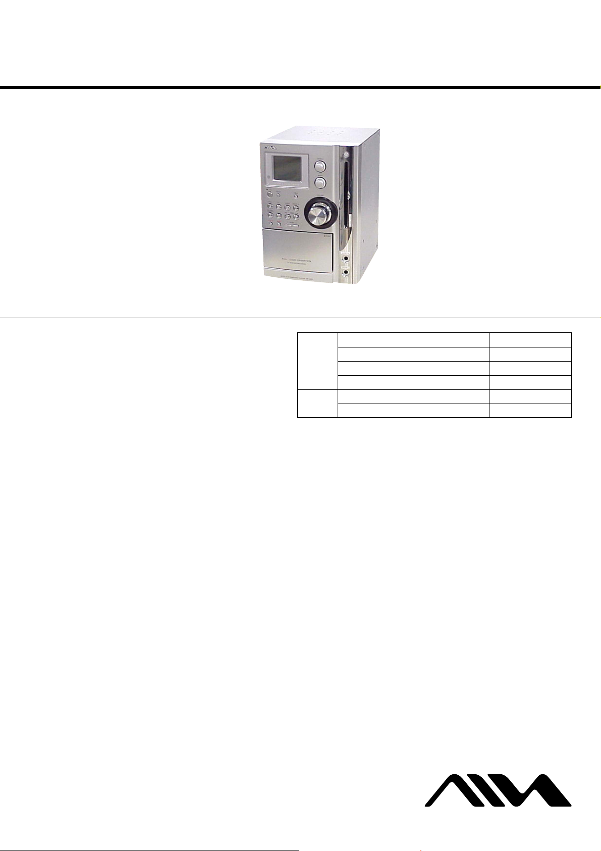
CX-LDB30/LDB50 are the Amplifier, CD player,
Tape Deck and Tuner section in XR-DB30/DB50.
CD CD Mechanism Type CDM80BV-F4BD81
Section Base Unit Name BU-F4BD81B
TAPE Model Name Using Similar Mechanism CX-LEM330
Section Tape Transport Mechanism T ype CMAL5Z220A
AEP Model
CX-LDB30/LDB50
UK Model
CX-LDB30
E Model
CX-LDB30/LDB50
Model Name Using Similar Mechanism NEW
Optical Pick-up Name KSM-215CFP/C2NP
CX-LDB50
European model:
DIN power output (rated): 60 + 60 W
(6 ohms at 1 kHz, DIN)
Continuous RMS power output (reference):
80 + 80 W
(6 ohms at 1 kHz, 10%
THD)
Music power output (reference):
200 + 200 W
(6 ohms at 1 kHz, 10%
THD)
Other models:
The following measured at AC 220 – 240 V, 50/60 Hz
DIN power output (rated): 60 + 60 W
(6 ohms at 1 kHz, DIN)
Continuous RMS power output (reference):
80 + 80 W
(6 ohms at 1 kHz, 10%
THD)
SPECIFICATIONS
CX-LDB30
European model:
DIN power output (rated): 45 + 45 W
(6 ohms at 1 kHz, DIN)
Continuous RMS power output (reference):
60 + 60 W
(6 ohms at 1 kHz, 10%
THD)
Music power output (reference):
140 + 140 W
(6 ohms at 1 kHz, 10%
THD)
Other models:
The following measured at AC 220 – 240 V, 50/60 Hz
DIN power output (rated): 45 + 45 W
(6 ohms at 1 kHz, DIN)
Continuous RMS power output (reference):
60 + 60 W
(6 ohms at 1 kHz, 10%
THD)
MICRO HI-FI COMPONENT SYSTEM
Inputs
AUDIO IN (RCA pin jacks):
Outputs
PHONES (stereo mini jack):
SPEAKER: accepts impedance of
CD player section
System Compact disc and digital
Laser Diode Properties Emission duration:
*This output is the value measurement at a distance of
200 mm from the objective lens surface on the
Optical Pick-up Block with 7 mm aperture
Sensitivity 700 mV,
impedance 47 kilohms
accepts headphones with
an impedance of 32 ohms
or more
6ohms
audio system
continuous
Laser Output*: Less than
µW
44.6
— Continued on next page —
9-879-476-02
2005D16-1
© 2005.04
Sony Corporation
Personal Audio Group
Published by Sony Engineering Corporation
Page 2

CX-LDB30/LDB50
Frequency response 20 Hz – 20 kHz
Signal-to-noise ratio More than 90 dB
Dynamic range More than 90 dB
Tape deck section
Recording system 4-track 2-channel stereo
Frequency response 100 – 10,000 Hz, using
Sony TYPE I cassettes
Tuner section
FM stereo, FM/AM superheterodyne tuner
FM tuner section
Tuning range 87.5 – 108.0 MHz
(50-kHz step)
Antenna FM lead antenna
Antenna terminals 75 ohms unbalanced
Intermediate frequency 10.7 MHz
AM tuner section
Tuning range
European model: 531 – 1,602 kHz
(with the tuning interval
set at 9 kHz)
Other models: 530 – 1,710 kHz
(with the tuning interval
set at 10 kHz)
531 – 1,602 kHz
(with the tuning interval
set at 9 kHz)
Antenna AM loop antenna, external
antenna terminal
Intermediate frequency 450 kHz
General
Power requirements
European model: AC 230 V, 50/60 Hz
Other models: AC 120, 220 or
230 – 240 V, 50/60 Hz
Adjustable with voltage
selector
Power consumption
XR-DB50
European model: 85 W
0.3 W (in Power Saving
mode)
Other models: 85 W
XR-DB30
European model: 70 W
0.3 W (in Power Saving
mode)
Other models: 70 W
Dimensions (w/h/d) excl. speakers:
Approx. 190 x 277 x
269 mm
Mass excl. speakers
CX-LDB50: 5.4 kg
CX-LDB30: 5.1 kg
Design and specifications are subject to change
without notice.
•Standby power consumption: 0.3 W
•Halogenated flame retardants are not
used in the certain printed wiring boards.
•Lead-free solder is used for soldering
certain parts.
•Halogenated flame retardants are not
used in cabinets.
SAFETY-RELATED COMPONENT WARNING!!
COMPONENTS IDENTIFIED BY MARK 0 OR DOTTED LINE
WITH MARK 0 ON THE SCHEMATIC DIAGRAMS AND IN
THE PARTS LIST ARE CRITICAL TO SAFE OPERATION.
REPLACE THESE COMPONENTS WITH SONY PARTS WHOSE
PART NUMBERS APPEAR AS SHOWN IN THIS MANUAL OR
IN SUPPLEMENTS PUBLISHED BY SONY.
2
Page 3

TABLE OF CONTENTS
CX-LDB30/LDB50
1. SERVICING NOTES ................................................ 4
2. GENERAL ................................................................... 5
3. DISASSEMBLY
3-1. Disassembly Flow ........................................................... 7
3-2. Side Panel (L)(R), Top Panel, Back Panel ....................... 8
3-3. CD Mechanism Section ................................................... 8
3-4. Front Panel Section ......................................................... 9
3-5. Power Transformer .......................................................... 9
3-6. MAIN Board.................................................................... 10
3-7. PANEL Board, CD EJECT Board, JACK Board ............ 10
3-8. Cassette Deck Mechanism............................................... 11
3-9. Cassette Panel .................................................................. 11
3-10. CD Mechanism Deck (CDM80BV-F4BD81) ................. 12
3-11. Chassis (Top) ................................................................... 12
3-12. Lever (Loading R/L)........................................................ 13
3-13. Disc Stop Lever, Disc Sensor Lever ................................ 14
3-14. DRIVER Board ............................................................... 14
3-15. BD Board ......................................................................... 15
3-16. Optical Pick-up (KSM-215CFP/C2NP) .......................... 15
3-17. Base Unit (BU-F4BD81B) .............................................. 16
3-18. Lever (BU Lock) ............................................................. 16
3-19. Close Lever ...................................................................... 17
3-20. DIR Lever, Gear (IDL-B) ................................................ 17
3-21. Gear (IDL-C) ................................................................... 18
4. TEST MODE ............................................................... 19
5. MECHANICAL ADJUSTMENTS......................... 20
6. ELECTRICAL ADJUSTMENTS .......................... 20
7. DIAGRAMS
7-1. Block Diagram — BD Section — ................................... 25
7-2. Block Diagram — MAIN Section — .............................. 26
7-3. Printed Wiring Board — BD Board — ........................... 27
7-4. Schematic Diagram — BD Board — .............................. 28
7-5. Printed Wiring Board
— DRIVER Board, JACK Board — ............................... 29
7-6. Schematic Diagram
— DRIVER Board, JACK Board — ............................... 30
7-7. Printed Wiring Board — MAIN Section (1/2) — ........... 31
7-8. Printed Wiring Board — MAIN Section (2/2) — ........... 32
7-9. Schematic Diagram — MAIN Section (1/5) — .............. 33
7-10. Schematic Diagram — MAIN Section (2/5) — .............. 34
7-11. Schematic Diagram — MAIN Section (3/5) — .............. 35
7-12. Schematic Diagram — MAIN Section (4/5) — .............. 36
7-13. Schematic Diagram — MAIN Section (5/5) — .............. 37
7-14. Printed Wiring Board — PANEL Board — .................... 38
7-15. Schematic Diagram — PANEL Board — ....................... 39
7-16. Printed Wiring Board — PT Board — ............................ 40
7-17. Schematic Diagram — PT Board — ............................... 41
8. EXPLODED VIEWS
8-1. Panel Section ................................................................... 47
8-2. Front Panel Section ......................................................... 48
8-3. Chassis Section ................................................................ 49
8-4. CD Mechanism Deck Section 1 (CDM80BV-F4BD81) . 50
8-5. CD Mechanism Deck Section 2 (CDM80BV-F4BD81) . 51
8-6. CD Mechanism Deck Section 3 (CDM80BV-F4BD81) . 52
8-7. Base Unit Section ............................................................ 53
9. ELECTRICAL PARTS LIST .................................. 54
3
Page 4
CX-LDB30/LDB50
SECTION 1
SERVICING NOTES
Notes on chip component replacement
• Never reuse a disconnected chip component.
• Notice that the minus side of a tantalum capacitor may be
damaged by heat.
Flexible Circuit Board Repairing
• Keep the temperature of the soldering iron around 270 °C
during repairing.
• Do not touch the soldering iron on the same conductor of the
circuit board (within 3 times).
• Be careful not to apply force on the conductor when soldering
or unsoldering.
UNLEADED SOLDER
Boards requiring use of unleaded solder are printed with the leadfree mark (LF) indicating the solder contains no lead.
(Caution: Some printed circuit boards may not come printed with
the lead free mark due to their particular size)
: LEAD FREE MARK
Unleaded solder has the following characteristics.
• Unleaded solder melts at a temperature about 40 °C higher
than ordinary solder.
Ordinary soldering irons can be used but the iron tip has to be
applied to the solder joint for a slightly longer time.
Soldering irons using a temperature regulator should be set to
about 350 °C.
Caution: The printed pattern (copper foil) may peel away if
the heated tip is applied for too long, so be careful!
• Strong viscosity
Unleaded solder is more viscou-s (sticky, less prone to flow)
than ordinary solder so use caution not to let solder bridges
occur such as on IC pins, etc.
• Usable with ordinary solder
It is best to use only unleaded solder but unleaded solder may
also be added to ordinary solder.
CAUTION
Use of controls or adjustments or performance of procedures
other than those specified herein may result in hazardous radiation
exposure.
This appliance is classified as a CLASS 1 LASER product.
The CLASS 1 LASER PRODUCT MARKING is located on the
exterior.
Laser component in this product is capable of emitting radiation
exceeding the limit for Class 1.
NOTES ON HANDLING THE OPTICAL PICK-UP
BLOCK OR BASE UNIT
The laser diode in the optical pick-up block may suffer electrostatic
break-down because of the potential difference generated by the
charged electrostatic load, etc. on clothing and the human body.
During repair, pay attention to electrostatic break-down and also
use the procedure in the printed matter which is included in the
repair parts.
The flexible board is easily damaged and should be handled with
care.
NOTES ON LASER DIODE EMISSION CHECK
The laser beam on this model is concentrated so as to be focused on
the disc reflective surface by the objective lens in the optical pickup block. Therefore, when checking the laser diode emission,
observe from more than 30 cm away from the objective lens.
LASER DIODE AND FOCUS SEARCH OPERATION
CHECK
Carry out the “S curve check” in “CD section adjustment” and check
that the S curve waveforms is output three times.
4
Page 5
SECTION 2
GENERAL
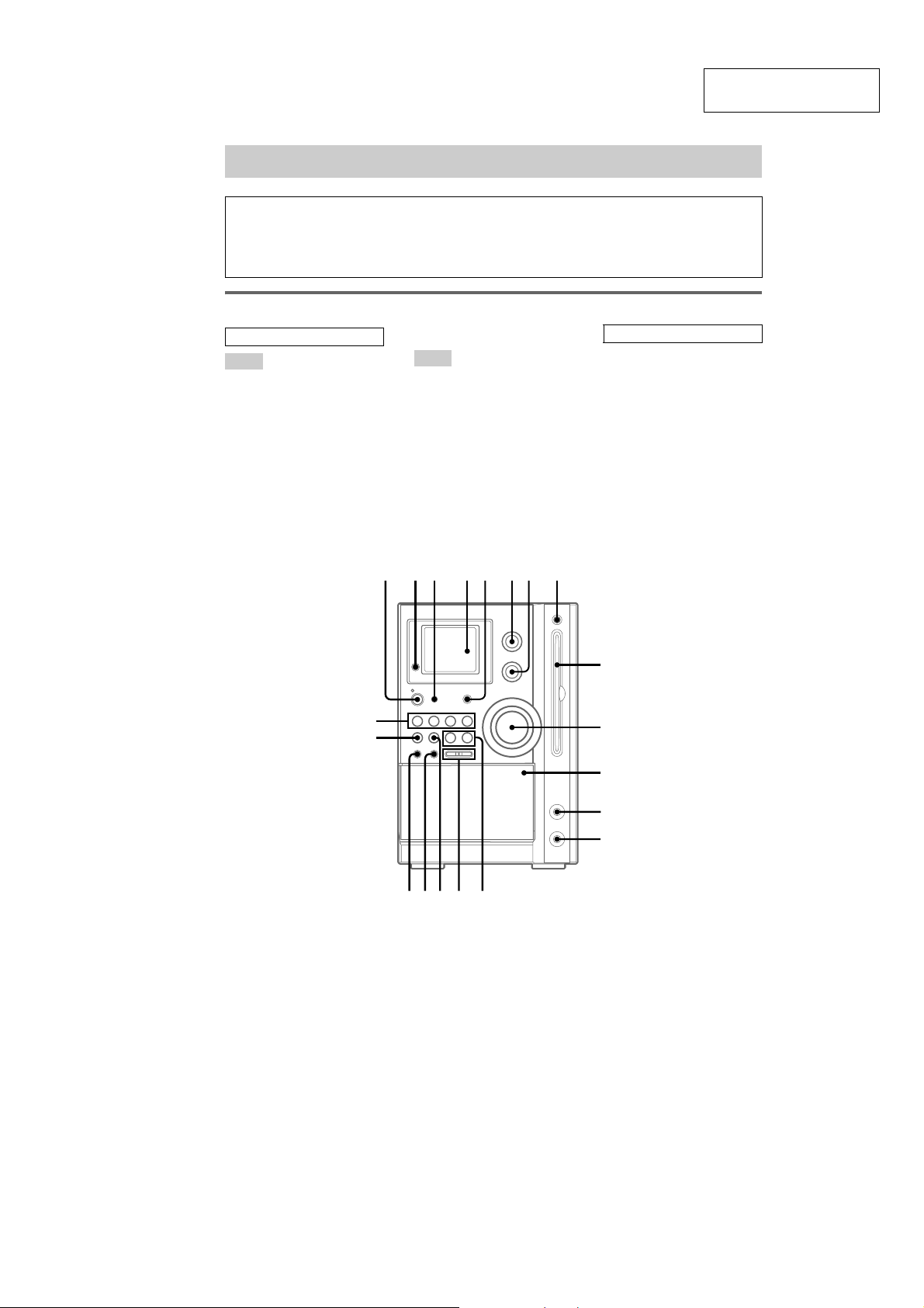
List of button locations and reference pages
CX-LDB30/LDB50
This section is extracted
from instruction manual.
How to use this page
Use this page to find the location of buttons and other
parts of the system that are mentioned in the text.
Main unit
ALPHABETICAL ORDER
A – O
AUDIO IN w; (17, 23, 27)
AUDIO IN jack qs (19, 23)
BASS control 7 (17)
CD SYNC qk (16)
Disc slot 9
DISPLAY 3 (15, 21, 22)
Display window 4
FOLDER +/– qg (10, 11, 16)
i-Bass 5 (17)
P – Z
PHONES jack qd
PLAY MODE ql (10, 11, 16, 26)
Remote sensor 2
TREBLE control 6 (17)
TUNER/BAND w; (12, 14, 17)
TUNING +/– qf (12, 14)
TUNING MODE ql (12, 14)
VOLUME control q; (18, 25)
1
23 4 5 67 8
Illustration number
r
DISPLAY ws (15, 21)
Name of button/part Reference page
RR
BUTTON DESCRIPTIONS
?/1 (power) 1 (7, 14, 27)
Z CD (eject) 8 (8, 9)
Z PUSH qa (16)
./> (go back/go forward)
qf (10)
m/M (rewind/fast forward)
qf (8, 10, 14, 16)
x (stop) qh (10, 13, 16)
z REC PAUSE/START qj (16)
TAPE/N (play) w; (16)
CD/NX (play pause) w; (10)
w;
ql
qk
HHS
sjJ
qh
qj
qg
9
q;
qa
qs
qd
qf
5
Page 6
CX-LDB30/LDB50
Remote control
ALPHABETICAL ORDER
A – O
CD qh (9, 11, 13, 16, 17)
CLEAR qd (12)
CLOCK/TIMER SELECT 2
(19, 20, 25)
CLOCK/TIMER SET 3 (8, 18,
19)
DISPLAY ql (15, 21, 22)
ENTER 9 (8, 11, 13, 18, 19)
EQ qs (17)
FM MODE 4 (15, 27)
FOLDER +/– qa (10, 11, 16)
FUNCTION 6 (8, 9, 11, 12, 14,
16, 17, 23, 27)
P – Z
PLAY MODE qk (10, 11, 16, 26,
28)
REPEAT 4 (11)
SLEEP w; (18)
TAPE qg (16, 17)
TUNER/BAND 5 (12, 14, 17)
TUNER MEMORY qj (13)
TUNING MODE qk (12, 14)
VOLUME +/– q; (18, 25)
w;
ql
qk
qj
qh
qg
qf
BUTTON DESCRIPTIONS
?/1 (power) 1 (7, 14, 19)
m/M (rewind/fast forward)
7 (10, 14, 16)
X (pause) 8 (10, 16)
x (stop) 8 (10, 16)
N (play) 8 (10, 16)
–/+(tuning) qf (12, 17)
./> (go back/go forward)
qf (8, 10, 18)
1
2
3
4
5
6
7
qd
qs
qa
8
9
0
Setting the clock
Use buttons on the remote for the operation.
1
Press ?/1 to turn on the system.
2
Press CLOCK/TIMER SET.
3
Press . or > repeatedly to set the
hour.
4
Press ENTER.
5
Press . or > repeatedly to set the
minute.
6
Press ENTER.
The clock starts working.
To adjust the clock
1
Press CLOCK/TIMER SET.
2
Press . or > until "CLOCK SET?"
appears, then press ENTER.
3
Do the same procedures as step 3 to 6
above.
Notes
The clock settings are canceled when you disconnect
the power cord or if a power failure occurs.
You cannot set the clock in Power Saving Mode
(page 21).
6
Page 7
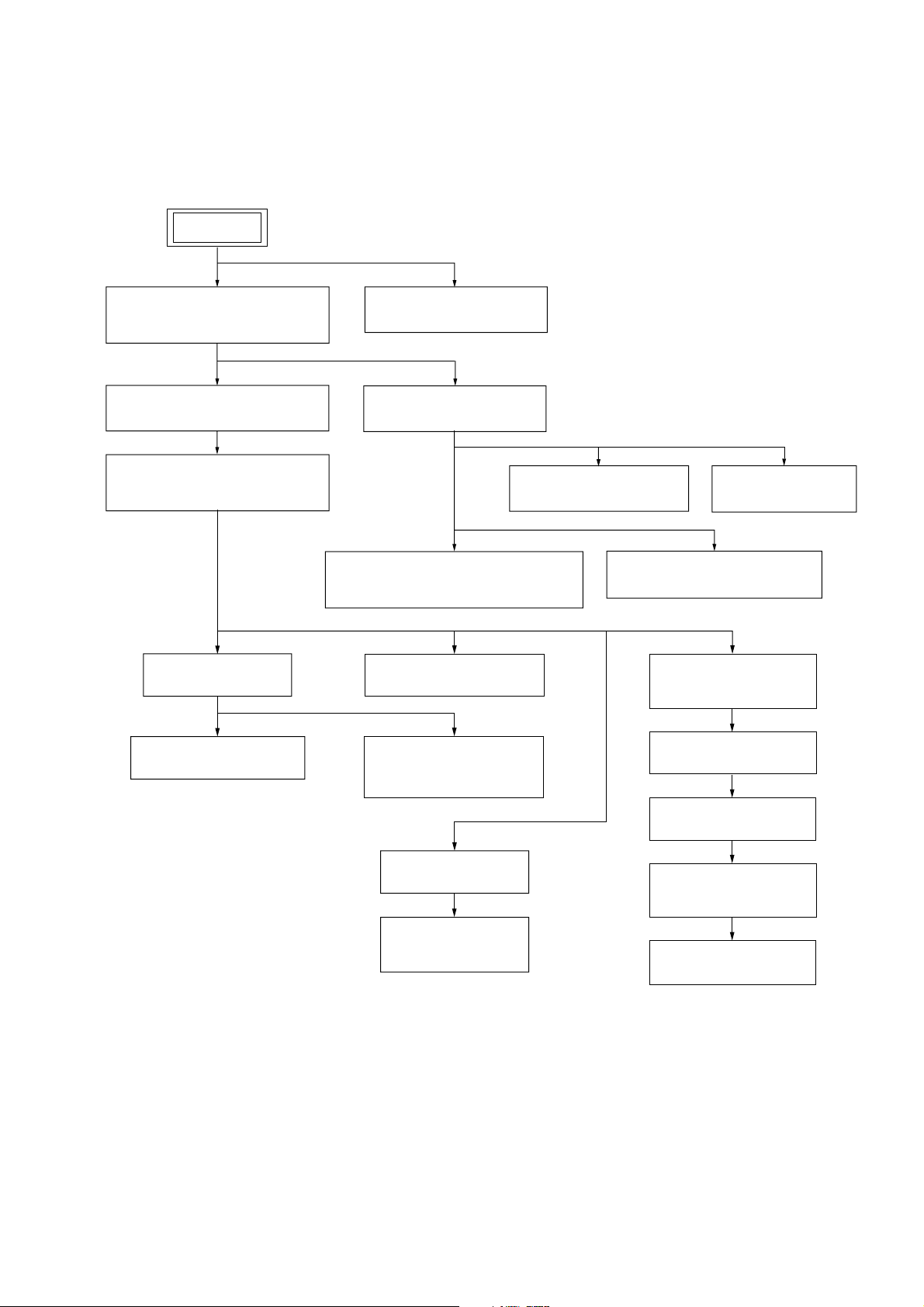
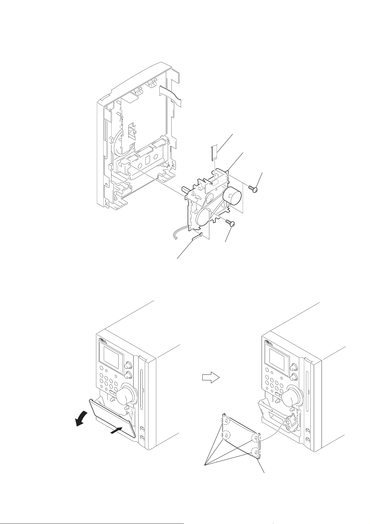
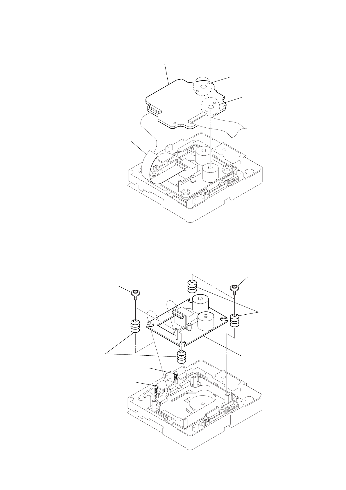
3-1. DISASSEMBLY FLOW
3-3.CD MECHANISM SECTION
(Page 8)
3-10.CD MECHANISM DECK
(CDM80BV-F4BD81)
(Page 12)
3-7.PANEL BOARD, CD EJECT BOARD,
JACK BOARD
(Page 10)
3-4.FRONT PANEL SECTION
(Page 9)
3-8.CASSETTE DECK MECHANISM
(Page 11)
3-6.MAIN BOARD
(Page 10)
3-5.POWER TRANSFORMER
(Page 9)
3-9.CASSETTE PANEL
(Page 11)
3-2.SIDE PANEL (L) (R), TOP PANEL,
BACK PANEL
(Page 8)
SET
3-11.CHASSIS (TOP)
(Page 12)
3-14.DRIVER BOARD
(Page 14)
3-17.BASE UNIT
(BU-F4BD81B)
(Page 16)
3-13.DISC STOP LEVER,
DISC SENSOR LEVER
(Page 14)
3-15.BD BOARD
(Page 15)
3-16.OPTICAL PICK-UP
(KSM-215CFP/C2NP)
(Page 15)
3-18.LEVER (BU LOCK)
(Page 16)
3-19.CLOSE LEVER
(Page 17)
3-20. DIR LEVER,
GEAR (IDL-B)
(Page 17)
3-21. GEAR (IDL-C)
(Page 18)
3-12.LEVER (LOADING R/L)
(Page 13)
•This set can be disassembled in the order shown below.
CX-LDB30/LDB50
SECTION 3
DISASSEMBLY
7
Page 8
CX-LDB30/LDB50
)
n
Note: Follow the disassembly procedure in the numerical order given.
3-2. SIDE PANEL (L)(R), TOP PANEL, BACK PANEL
qa
top panel
3
side panel (L)
2
three claws
8
screw
×
(QT2+3
10)
9
screw
(QT2+3
×
10)
qh
back panel
qg
connector
2p(CN292)
q;
screw (+BVTP3 × 10)
qs
two screws
(+BVTP3
qd
×
10)
two screws
(+BVTP3
qf
six screws
(+BVTP3
×
10)
×
10
1
four screws
(+BVTP3
×
10)
3-3. CD MECHANISM SECTION
3
screw
×
(QT2+3
5
claw
10)
7
6
side panel (R)
2
w
ire (flat type)
15core (CN602)
screw
(QT2+3
×
1
27core (CN902)
10)
w
ire (flat type)
4
six screws
(+BVTP3
5
three claws
×
10)
6
connector
7p(CN701)
4
two screws
(QT2+3 × 10)
7
CD mechanism sectio
8
Page 9
3-4. FRONT PANEL SECTION
1
w
ire (flat type)
19core (CN904)
2
w
ire (flat type)
8core (CN901)
7
screw
(QT2+3 × 10)
3
w
ire (flat type)
7core (CN905)
4
connector
7p (CNA302)
CX-LDB30/LDB50
9
two claws
0
front panel section
3-5. PO WER TRANSFORMER
6
tapping screw (B3)
7
two claws
4
connector
8p (CN002)
qa
power transformer
8
holder
0
8
screw
(QT2+3 × 10)
(pwb PT)
9
6
four
screws
qs
plate
2
15core
two
tapping screws (B3)
(PT shield)
w
ire (flat type)
5
screw (+B3)
3
tuner (FM/AM)
5
2p (CN001)
1
connector
tapping screw (B3)
9
Page 10
CX-LDB30/LDB50
)
)
3-6. MAIN BOARD
7
two
screws (B3)
8
two
screws (B3)
tapping
tapping
0
MAIN board
2
two
screws (+BV3)
5
tapping screw (B3)
clamp
4
w
ire (flat type)
15core (CN602)
9
heat sink (main)
6
two
tapping screws (B3)
3
screw (+BV3
1
connector
8p (CN002)
3-7. PANEL BOARD, CD EJECT BOARD, JACK BOARD
0
CD EJECT board
6
knob (VOL)
5
two knobs B/T
8
claw
7
tapping screw (B2.6)
qa
19core (CN502)
w
ire (flat type)
qs
PANEL board
9
eleven
tapping screws (B2.6
10
4
JACK board
2
holder board
1
two
tapping screws (B3)
3
w
ire (flat type)
9core (CN203)
Page 11
3-8. CASSETTE DECK MECHANISM
4
w
ire (flat type) 7core
5
CX-LDB30/LDB50
cassette deck mechanism
3
two screws
(B3)
3-9. CASSETTE PANEL
2
Open the
cassette panel.
1
Push the
cassette panel.
2
clamp
1
two screws
(B3)
3
four claws
4
cassette panel
11
Page 12
CX-LDB30/LDB50
k
)
)
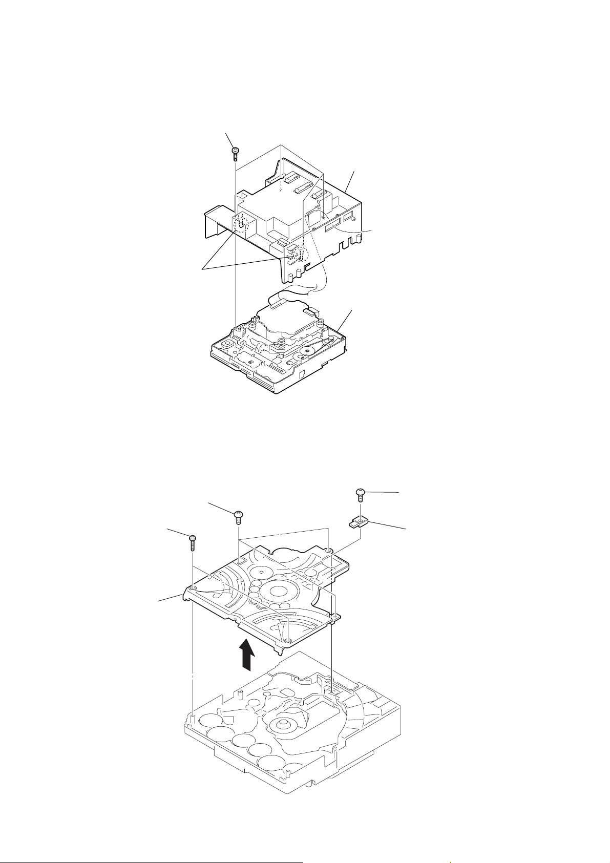
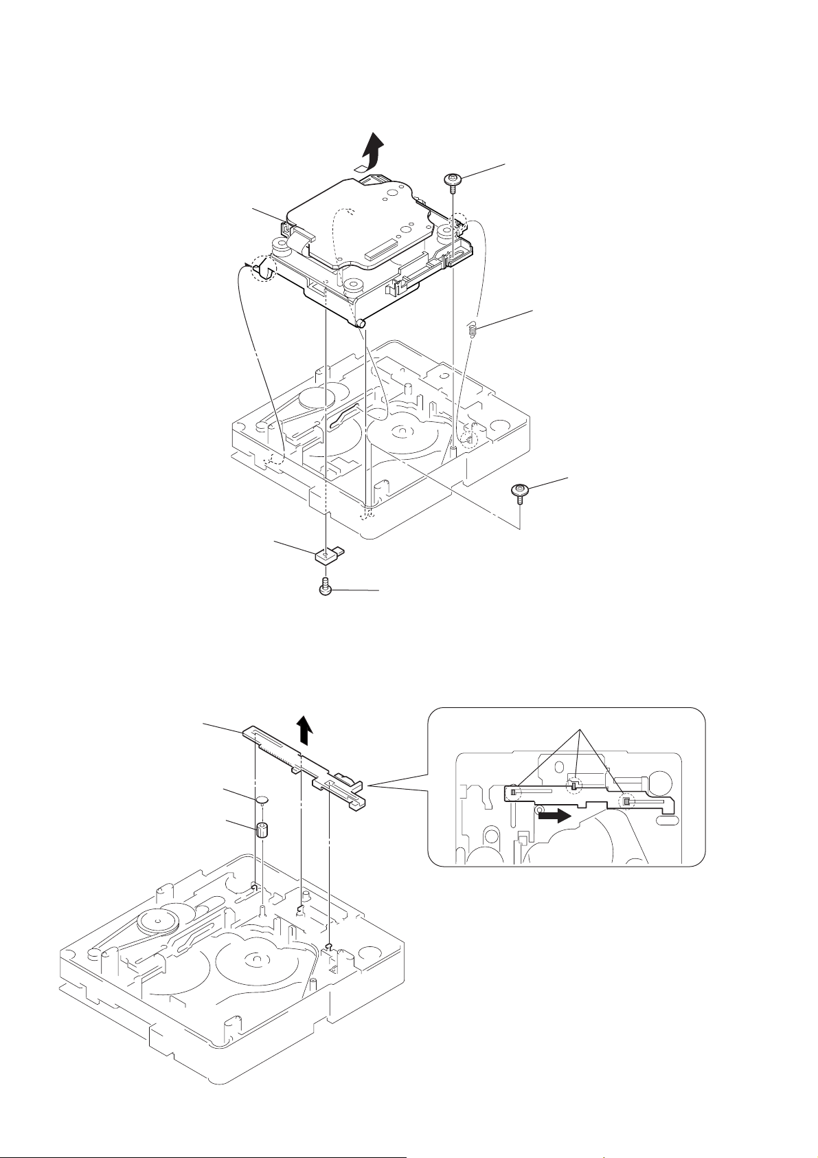
3-10. CD MECHANISM DECK (CDM80BV-F4BD81)
1
four
tapping screws (B3)
2
two claws
3
CD HOLDER
4
CD mechanism dec
(CDM80BV-F4BD81
3-11. CHASSIS (TOP)
3
two screws
(+P 2
5
chassis (top)
4
three screws
(+BVTP 2.6
×
10)
1
×
8)
screw
(+BVTP 2.6
2
lever (CL UP2
×
8)
12
Page 13
)
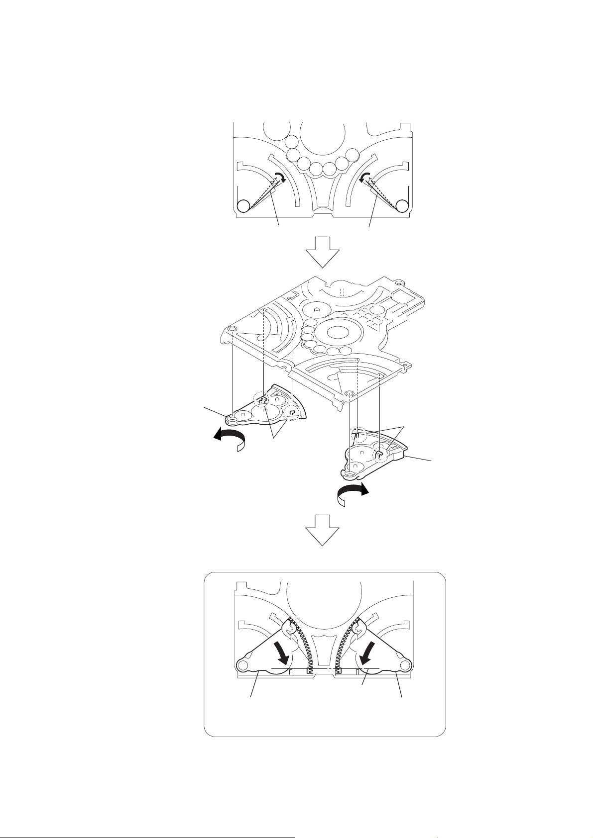
3-12. LEVER (LOADING R/L)
CX-LDB30/LDB50
5
lever (loading-R)
1
torsion spring (loading LV) torsion spring (loading RV)
4
two hooks
1
2
two hooks
3
lever (loading-L
PRECAUTION DURING LEVER (LOADING R / L) INSTALLATION
Align the horizontal position.
lever (loading-L)
Install the
both levers so that they move symmetrically.
lever (loading-R)
13
Page 14
CX-LDB30/LDB50
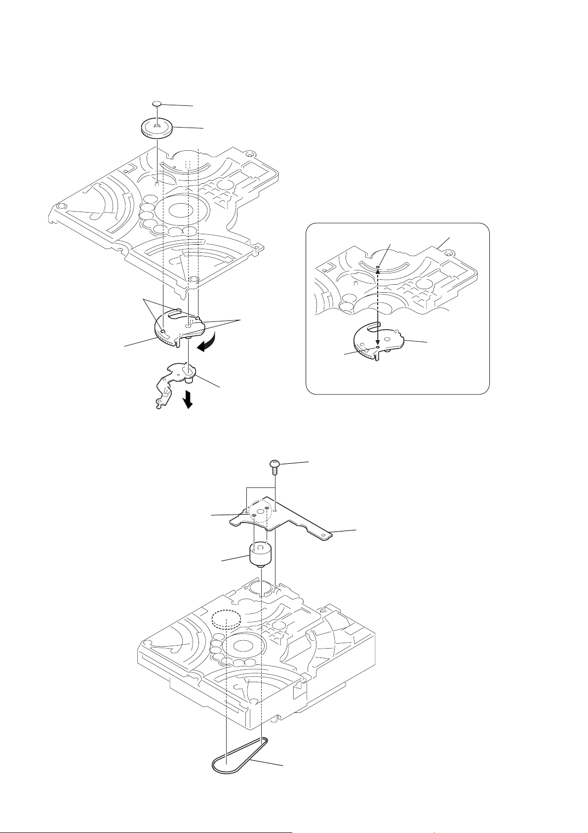
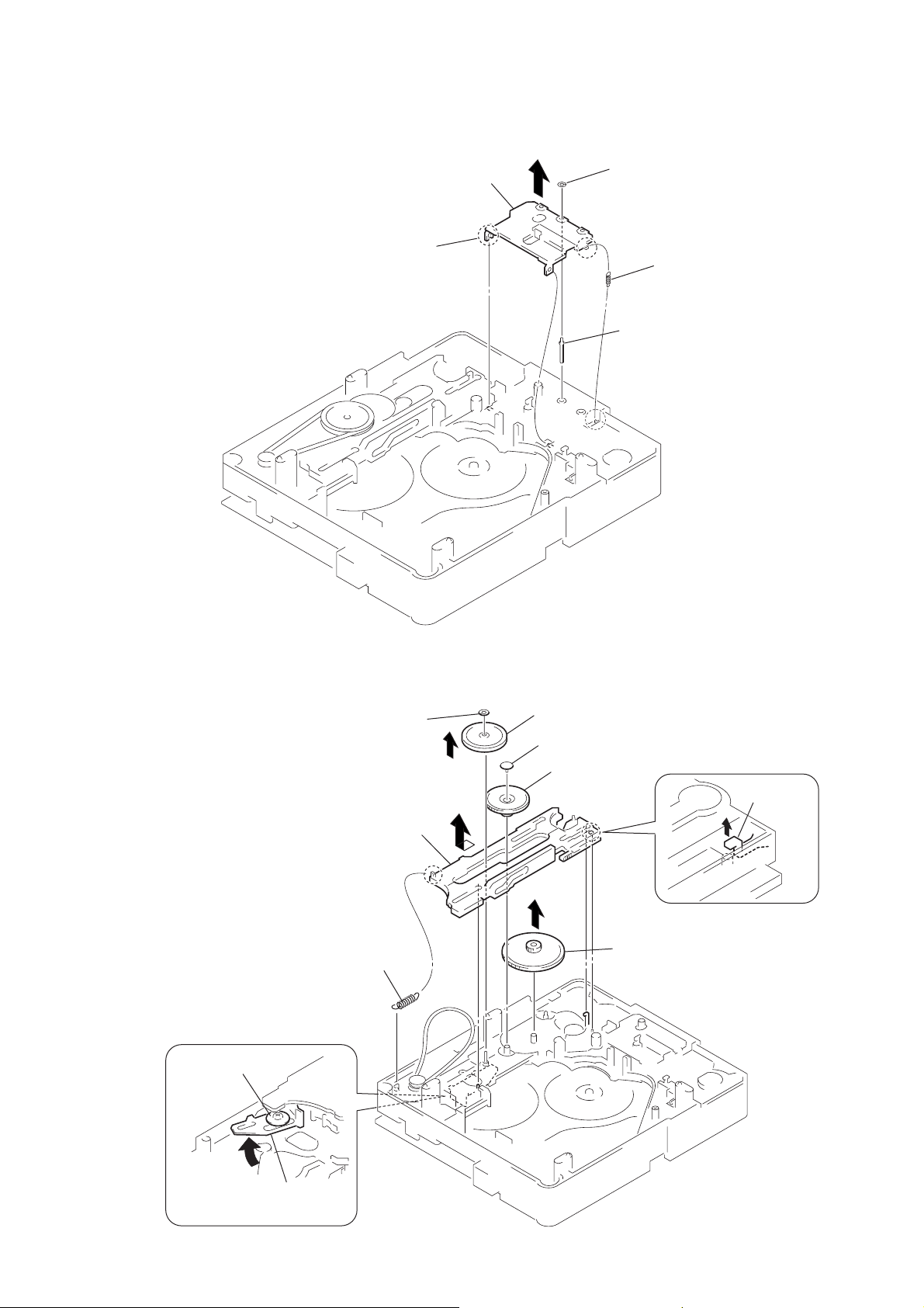
3-13. DISC STOP LEVER, DISC SENSOR LEVER
1
gear (cap)
2
gear (IDL-L)
PRECAUTION DURING DISC STOP LEVER INSTALLATION
5
two hooks
6
disc stop lever
3-14. DRIVER BOARD
3
Remove soldering
from the two points.
3
two claws
4
disc sensor lever
hole
hole
Install the disc stop lever so that the both holes
are aligned.
2
two screws
(+BVTP 2.6
×
8)
5
DRIVER board
chassis (top)
disc stop lever
14
4
motor (pulley) assy
1
belt (MOT)
Page 15
s
3-15. BD BOARD
1
CN101
4
B
D board
CX-LDB30/LDB50
3
Remove the two solderings.
2
Remove the two solderings.
3-16. OPTICAL PICK-UP (KSM-215CFP/C2NP)
3
two floating screws
(+PTPWHM 2.6)
6
two insulators
2
tension spring (F-2)
1
tension spring (F-1)
4
two floating screws
(+PTPWHM 2.6)
5
two insulator
7
optical pick-up
(KSM-215CFP/C2NP)
15
Page 16
CX-LDB30/LDB50
3-17. BASE UNIT (BU-F4BD81B)
6
base unit
(BU-F4BD81B)
4
floating screw
(+PTPWHM 2.6)
3
holder down b spring
3-18. LEVER (BU LOCK)
5
lever (BU lock)
1
gear (cap)
2
gear (BU lock)
2
lever (CL UP2)
1
screw
(+BVTP 2.6
5
floating screw
(+PTPWHM 2.6)
×
8)
4
three hooks
3
16
Page 17
g
3-19. CLOSE LEVER
3
claw
5
close lever
1
washer (3-1-0.4)
2
close lever sprin
4
shaft disc stop
CX-LDB30/LDB50
3-20. DIR LEVER, GEAR (IDL-B)
2
capstan retaining ring
1
tension coil spring (DIR)
6
Loosen the screw.
9
DIR lever
3
gear pulley
4
gear (cap)
5
gear (IDL-A)
0
gear (IDL-B)
8
stopper
7
Hold the release lever
and change the direction.
17
Page 18

CX-LDB30/LDB50
3-21. GEAR (IDL-C)
3
gear (IDL-D)
2
1
gear (IDL-F)
7
gear (IDL-C)
6
two claws
claw
4
three hooks
5
gear loading lever
18
Page 19

SECTION 4
TEST MODE
CX-LDB30/LDB50
[COLD RESET]
* The cold reset clears all data including preset data stored in
the RAM to initial conditions. Execute this mode when
returning the set to the customer.
Procedure:
1. Press the ?/1 button to turn off the main power.
2. Press two buttons of [AUDIO IN] and ?/1 simultaneously for
more than two seconds.
3. The fluorescent indicator tube does not display any message
and the set is reset.
[COMMON TEST]
*This mode is used to check the function of the amplifier.
Procedure:
1. Press the ?/1 button to turn the set on.
2. Press two buttons of x and [DISPLAY] simultaneously for
more than two seconds.
3. The message “Volume MAX” is displayed, when the
[VOLUME] knob is rotated clockwise. The message “Volume
MIN” is displayed, when the [VOLUME] knob is rotated
counterclockwise.
4. Each time the [BASS] or [TREBLE] knob is turned or Press the
[EQ] button (RM), the message “TONE MAX”, “TONE MIN”
or “TONE FLAT” is displayed in this order.
[P ANEL TEST]
*The panel test, the version, and inducing is displayed.
Procedure:
1. Press the ?/1 button to turn off the main power.
2. Press two buttons of [AUDIO IN] and [DISPLAY] simultaneously
for more than two seconds.
3. All lighting display is done.
4. 4-1. To enter the test mode, press the button [i-Bass]
simultaneously.
The version of the microcomputer is displayed.
4-2. To enter the key test mode, press the button [PLAY MODE/
TUNING MODE] simultaneously.
The version of the microcomputer is displayed.
5. Press two buttons of [AUDIO IN] and [DISPLAY] simultaneously
for more than two seconds, it ends.
[CD Repeat 5 Times Limit Release Mode]
Procedure:
1. Press the ?/1 button to turn the set on.
2. Select the FUNCTION to CD.
3. Press two buttons of Z CD and [PLAY MODE/TUNING MODE]
simultaneously for more than two seconds.
4. The repeat all mark blinks and then repeat 5 times limit is
released.
[Disc anti-theft]
Procedure:
1. Press the ?/1 button to turn the set on.
2. Set the FUNCTION to CD.
3. Press two buttons of x and Z CD simultaneously for more
than five seconds.
4. Press two buttons of x and Z CD simultaneously for more
than five seconds to turn the set off.
[CD ERROR CODE]
Procedure:
1. Press the ?/1 button to turn the set on.
2. Set the FUNCTION to CD.
3. Press two buttons of CD u and [DISPLAY] simultaneously
for more than two seconds.
4. Switch the CDM/NO DISC using > , . .
Advance the number using > , Reverse the number using
. .
[CD SERVICE MODE Mode]
*This mode can run the CD sled motor freely. Use this mode,
for instance, when cleaning the pickup.
Procedure:
1. Press the ?/1 button to turn the set on.
2. Set the FUNCTION to CD.
3. While depressing the CD u button, Press the [i-Bass] button.
The message “SERVICE MODE” is displayed.
4. With the CD in stop status, press the > button to move the
pickup to outside track, or press the . button to inside
track.
5. When press the CD u button, normal playback is
performed.
6. Each time the CD u button is pressed during normal
playback, the tracking servo is switched on or off.
7. To exit this mode, either change to other functions or extract
an AC plug.
[AM Channel Step 9 kHz/10kHz Selection Mode]
* Either the 9 kHz step or 10 kHz step can be selected for the
AM channel step.
Procedure:
1. Turn on the power, and press the [TUNER] button to select the
AMP band.
2. Turn off the power.
3Press the > button and the ?/1 button at the same time to
enter this mode.
[CD Ship Mode and Memory clear]
*This mode moves the optical pick-up to the position durable
to vibration and Memory Clear. Use this mode when returning
the set to the customer after repair.
Procedure:
1. Press the ?/1 button to turn the set on.
2. Set the FUNCTION to CD.
3. Press two buttons of Z CD and > simultaneously for
more than two seconds.
4. After a message “MECHA LOCK” is displayed on the
fluorescent indicator tube, the CD ship mode is set and the
power is turned off.
19
Page 20
CX-LDB30/LDB50
set
MAIN board
SPEAKER terminal (J201)
L-CH, R-CH
+
–
level meter
test tape
P-4-A100
(10 kHz, –10 dB)
SECTION 5
MECHANICAL ADJUSTMENTS
SECTION 6
ELECTRICAL ADJUSTMENTS
TAPE MECHANISM DECK SECTION
Precaution
1. Clean the following parts with a denatured alcohol-moistened
swab:
record/playback heads pinch rollers
erase head rubber belts
capstan idlers
2. Demagnetize the record/playback head with a head demagnetizer.
3. Do not use a magnetized screwdriver for the adjustments.
4. After the adjustments, apply suitable locking compound to
the parts adjusted.
5. The adjustments should be performed with the rated power
supply voltage unless otherwise noted.
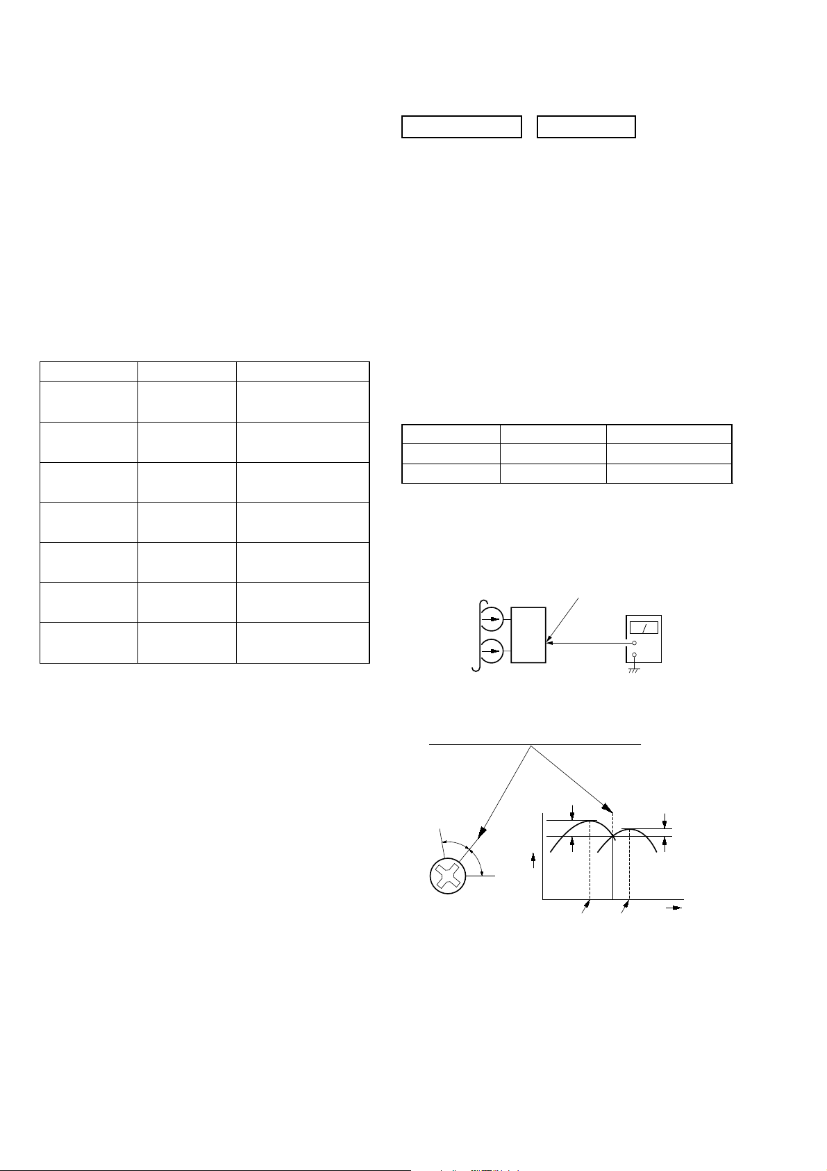
Torque Measurement
Mode
FWD
FWD
back tension
REV
REV
back tension
FF/REW
FWD tension
REV tension
Torque meter Meter reading
2.94 – 7.84 mN • m
CQ-102C
CQ-102C
CQ-102RC
CQ-102RC
CQ-201B
CQ-403A
CQ-403R
(30 to 79 g • cm)
(0.42 – 1.11 oz • inch)
0.15 – 0.59 mN • m
(2 to 6 g • cm)
(0.03 – 0.08 oz • inch)
2.94 – 7.84 mN • m
(30 to 79 g • cm)
(0.42 – 1.11 oz • inch)
0.15 – 0.59 mN • m
(2 to 6 g • cm)
(0.03 – 0.08 oz • inch)
6.86 – 17.64 mN • m
(70 to 179 g • cm)
(0.98 – 2.49 oz • inch)
9.8 mN • m or more
(100 g • cm or more)
(1.4 oz • inch or more)
9.8 mN • m or more
(100 g • cm or more)
(1.4 oz • inch or more)
DECK SECTION 0 dB=0.775V
Precaution
1. Demagnetize the record/playback head with a head
demagnetizer.
2. Do not use a magnetized screwdriver for the adjustments.
3. After the adjustments, apply suitable locking compound to
the parts adjusted.
4. The adjustments should be performed with the rated power
supply voltage unless otherwise noted.
5. The adjustments should be performed in the order given in
this service manual. (As a general rule, playback circuit
adjustment should be completed before performing recording
circuit adjustment.)
6. The adjustments should be performed for both L-CH and RCH.
7. Switches and controls should be set as follows unless otherwise
specified.
• Test Tape
Signal Used forTape
P-4-A100
WS-48B
Record/Playback Head Azimuth Adjustment
Procedure:
1. Mode : Playback
10 kHz, –10 dB
3 kHz, 0 dB
Azimuth Adjustment
Tape Speed Check
2. Turn the adjustment screw and check output peaks. If the peaks
do not match for L-CH and R-CH, turn the adjustment screw
so that outputs match within 1 dB of peak.
Output
level
within
1dB
L-CH
peak
R-CH
peak
within
1dB
Screw
position
L-CH
peak
Screw
position
R-CH
peak
20
Page 21

CX-LDB30/LDB50
)
attenuator
set
MAIN board
AUX IN (J291)
1) 315 Hz
2) 10 kHz
50 mV (–23.8 dB)
600
Ω
blank tape
CN-123
AF OSC
3. Mode: Playback
test tape
P-4-A100
(10 kHz, –10 dB)
L-CH
set
R-CH
in phase 45°90°135°180
MAIN board
SPEAKER terminal (J201)
L-CH
R-CH
waveform of oscilloscope
good
oscilloscope
wrong
H
V
°
4. After the adjustments, apply suitable locking compound to
the parts adjusted.
Adjustment Location: Record/Playback/Erase Head
Record Bias Adjustment
Procedure:
1. Record mode
2. Mode: Playback
i-Bass OFF
BASS 0
TREBLE 0
recorded
portion
set
MAIN board speaker terminal (J201)
level meter
+
–
adjustment screw
Note: Refer to “3-9. Cassette Panel” (see page 11
Tape Speed Check
Mode: Playback
test tape
WS-48B
(3 kHz, 0 dB)
3. Confirm playback the signal recorded in step 1 become
adjustment level as follows.
Adjustment level: Playback output of 315 Hz to playback output
of 10 kHz: 0 ± 1.0 dB (0 ± 4.5mV).
frequency counter
Sample Value of Wow and flutter: 0.3% or less W.RMS (JIS)
set
MAIN board
SPEAKER terminal (J201)
L-CH, R-CH
+
–
1. Insert the WS-48B into deck.
2. Press the TAPE N button of deck.
3. Confirm that the frequency counter reads 3000 ± 90 Hz.
(WS-48B)
21
Page 22

CX-LDB30/LDB50
p
CD SECTION
Note:
1. Use YEDS-18 disc (3-702-101-01) unless otherwise indicated.
2. Use an oscilloscope with more than 10MΩ impedance.
3. Clean the object lens by an applicator with neutral detergent
when the signal level is low than specified value with the
following checks.
S-curve Check
Connection:
oscilloscope
BD board
TP (FED)
TP (VC)
Procedure:
1. Connect an oscilloscope to test point TP (FEO) and TP (VC)
on the BD board.
2. While depressing the CD u button, insert an AC plug.
3. Put the disc (YEDS-18) in and press the x button and actuate
the focus search. (actuate the focus search when disc table is
moving in and out)
4. Check the oscilloscope waveform (S-curve) is symmetrical
between A and B. And confirm peak to peak level within 2 ± 1
Vp-p.
S-curve waveform
+
–
A
B
symmetry
within 2
±
1 Vp-
RFDC signal waveform
VOLT/DIV: 200 mV
TIME/DIV: 500 ns
level: 0.6
±
0.15 Vp-p
Checking Location: BD board (Conductor Side)
RFAC Level Check
Connection:
oscilloscope
BD board
TP (RFACO)
TP (VC)
+
–
Procedure:
1. Connect an oscilloscope to test point TP (RFACO) and TP
(VC) on the BD board.
2. Turn the power on.
3. Put the disc (YEDS-18) in to playback the number five track.
4. Confirm that oscilloscope waveform is clear and check RFAC
signal level is correct or not.
Note: A clear RFAC signal waveform means that the shape “◊” can
be clearly distinguished at the center of the waveform.
RFAC signal waveform
VOLT/DIV: 200 mV
TIME/DIV: 500 ns
Note: •Try to measure several times to make sure than the ratio of A : B
or B : A is more than 10 : 7.
•Take sweep time as long as possible and light up the
brightness to obtain best waveform.
Checking Location: BD board (Conductor Side)
RFDC Level Check
Connection:
oscilloscope
BD board
TP (RFDCO)
TP (VC)
+
–
Procedure:
1. Connect an oscilloscope to test point (RFDCO) and TP (VC)
on the BD board.
2. Turn the power on.
3. Put the disc (YEDS-18) in to playback the number five track.
4. Confirm that oscilloscope waveform is clear and check RFDC
signal level is correct or not.
Note: A clear RFDC signal waveform means that the shape “◊” can
be clearly distinguished at the center of the waveform.
level: 1.0
Checking Location: BD board (Conductor Side)
±
0.4 Vp-p
22
Page 23

CX-LDB30/LDB50
)
E-F Balance Adjustment
Connection:
oscilloscope
BD board
TP (TEO)
TP (VC)
+
–
Procedure:
1. Connect an oscilloscpe to test point TP (TEO) and TP (VC)
on the BD board.
2. AC is put in pushing CD u button to enter the CD test
mode.
3. Put the disc (YEDS-18) in to playback the number five track.
4. Press the CD u button. If it plays, press the CD u button
again. (The tracking servo and the sledding servo are turned
OFF)
5. Check the level B of the oscilliscope’s waveform and the A
(DC voltage) of the center of the Traverse waveform.
Confirm the following :
A/B x 100 = less than ±10%
Traverse Waveform
0V
Center of
the waveform
B
A (DC
voltage
Checking Location:
– BD BOARD (Conductor Side) –
IC251
IC301
TP
(VC)
TP
(VEO)
TP
(FEO)
TP
(RFDCO)
IC101
TP
(RFACO)
IC303
level: 1.0 ± 0.5 Vp-p
6. Press the CD u button. (The tracking servo and sledding
servo are turned ON)
Rotate RV101 on BD board and adjust the C (DC voltage) is
almost equal to the A (DC voltage) in step 4.
7. To exit from this mode, turn the power off.
Notes:•Always move the optical pick-up to most inside track when exiting
0V
from this mode. Otherwise, a disc will not be unloaded.
• Do not run the sled motor excessively, otherwise the gear can be
chipped.
Traverse Waveform
Tracking servo
Sled servo
OFF
Tracking servo
Sled servo
ON
C (DC
voltage)
Checking Location: BD board (Conductor Side)
23
Page 24

CX-LDB30/LDB50
C
B
These are omitted.
E
Q
B
These are omitted.
CE
B
These are omitted.
CE
Q
• Circuit Boards Location
SECTION 7
DIAGRAMS
CD EJECT board
PANEL board
MAIN board
JACK board
BD board
DRIVER board
PT board
THIS NOTE IS COMMON FOR PRINTED WIRING BOARDS AND SCHEMATIC DIAGRAMS.
(In addition to this, the necessary note is printed in each block.)
For Schematic Diagrams.
Note:
• All capacitors are in µF unless otherwise noted. (p: pF)
50 WV or less are not indicated except f or electrolytics and
tantalums.
• All resistors are in Ω and 1/
specified.
• f : internal component.
• C : panel designation.
Note: The components identified by mark 0 or dotted
line with mark 0 are critical for safety.
Replace only with part number specified.
• A : B+ Line.
• B : B– Line.
•Voltages and waveforms are dc with respect to ground
under no-signal (detuned) conditions.
No mark: FM
•Voltages are taken with a VOM (Input impedance 10 MΩ).
Voltage variations may be noted due to normal production
tolerances.
•Waveforms are taken with a oscilloscope.
Voltage variations may be noted due to normal production
tolerances.
• Circled numbers refer to waveforms.
• Signal path.
F : TUNER
J : CD
d : AUX
E : PB (TAPE)
a : REC (TAPE)
•Abbreviation
E51 : Chilean and Peruvian model.
RU : Russian model.
4
W or less unless otherwise
For Printed Wiring Boards.
Note:
• X : parts extracted from the component side.
• Y : parts extracted from the conductor side.
• f : internal component.
• : Pattern from the side which enables seeing.
Caution:
Pattern face side: P arts on the pattern face side seen from
(Conductor Side) the pattern face are indicated.
Parts face side: Parts on the parts face side seen from
(Component Side) the parts face are indicated.
• Indication of transistor.
24
Page 25

CX-LDB30/LDB50
7-1. BLOCK DIAGRAM — BD SECTION —
DETECTOR
A
B
C
D
F
E
OPTICAL PICK-UP
BLOCK
(KSM-215CFP)
LASER DIODE
PD
I-V AMP
LD
M101
(SPINDLE)
M102
(SLED)
M
M
D +3.3V
AUTOMATIC
POWER
CONTROL
Q10
CH4OUTF
16
CH4OUTR
15
CH3OUTF
17
CH3OUTR
18
A
26
B
27
C
28
D
29
F
20
E
19
LD
36
MOTOR/COIL DRIVE
IC251
MOTOR
DRIVE
MOTOR
DRIVE
CH4IN
CH3FIN
CH3RIN
SUMMING
FOCUS
ERROR
TRACKING
ERROR AMP
APC LD
AMP
24
23
22
AMP
AMP
FILTER
CD DSP
IC101 (1/2)
OPIN+
CD DSP
IC101 (2/2)
EQ_
IN
RFAC
35
VCA
2
EQ
21 23
FEI
TEI
A/D
CONVERTER
RFACO
41
42
45
46
RFACI
ASYI
ASYO
DIGITAL
CLV
PROCESSOR
MDP
6
ASYMMETRY
CORRECTOR
100
AC_
RF
SUM
34
FEO
24
TEO
22
PD
37
OPOUT
27
XRST
51 53
FILI
PCO
FILO
CLTV
DIGITAL PLL
TO SERVO AUTO
SEQUENCER
CPU INTERFACE
DATA
CLOCK
XLAT
35
37 36
I-XLT
I-CLK
I-DATA
1125052
XPCK
DEMODULATOR
SUBCODE
PROCESSOR
EXCK
SCOR
SENS
SBSO
96 97
98 99115107102 105 104 110 111
56 19
I-MP3DAT
O-SCOR
O-MP3DAT
O-MP3CLK
I-MP3-ACK
I-MP3-REQ
I-MP3-STBY
O-SENS
EFM
SQCK
SQSO
I-MI-CS
O-MILT
MP3-RST
I-XTACN
32K
RAM
INTERNAL BUS
WFCK
XUGF
GFS
113
6
5
7
47
48
32
33
49
45
57
CORRECTOR
EMPH
EMPH1
68
69
MIDIO
6
MICK
7
MICS
4
MILP
5
MIACK
8
PO11/BUCK/AD14
36
STANDBY
3
RESET
2
ERROR
MP3 DECODER
IC301
D/A
DIGITAL
INTERFACE
117 93
C4M
SELECTOR
LRCK
63 66 65
16
19
18 14
SBSY/BCKIB
SFSY/LRCKIB
MP3
3.3V
GENERATOR
D/A
CONVERTER
BCK
PCMD
15
SDI0
BCKIA
LRCKIA
VDDT42VDDT
9
XTSL
CLOCK
LRCKI
BCKI
62 60 61
1
XTACN
AOUT1
AOUT2
PCMDI
11
SDO0
IC303
+1.5V REG
XTAO
XTAI
VDDP
VDD
VDDX
VDDX
77
78
95
81
86
1
21
40
57
5
R-CH
X171
16.9344MHz
CD
MAIN
A
SECTION
2-AXIS
DEVICE
(TRACKING)
(FOCUS)
14
13
12
11
CH1OUTF
CH1OUTR
CH2OUTF
CH2OUTR
COIL
DRIVE
COIL
DRIVE
MUTE
20
CH1FIN
CH1RIN
CH2FIN
CH2RIN
SFDR
9
SRDR
10
4
5
6
7
TFDR
11
TRDR
12
FFDR
13
FRDR
14
PWM GENERATOR
FOCUS/TRACKING/SLED
S101
(LIMIT)
FOCUS/
TRACKING/SLED
SERVO DSP
SSTP
7
MIRR,
DFCT, FOK
DETECTOR
SERVO
INTERFACE
SERVO AUTO
SEQUENCER
TO CPU INTERFACE
FOK
MIRR
DFCT
COUT
SCLK
3
1
2
LD OUT
LD IN
82
83
SYSTEM CONTROLLER
O-X-RST
IC901 (1/2)
I-CDMSW1
I-CDMSW2
I-CDMSW3
85
86
84
119
108
60
IC701 LOADING MOTOR DRIVE
FIN
7
OUT1
OUT2
9
RIN
S701 (DISC IN/OUT)
S702 (CHUKING)
S703 (TRIGGER)
4
2
M
(ON : When disc insert)S701
S702
(ON : Play position)
(ON : Play position)
S703
M701
(LOADING)
• R-ch is omitted due to same as L-ch
• Signal Path
: CD PLAY
CX-LDB30/LDB50
2525
Page 26

CX-LDB30/LDB50
7-2. BLOCK DIAGRAM — MAIN SECTION —
J291
AUDIO IN
A
CD SECTION
R-CH
TUNER PACK
L-CH
R-CH
D OUT
TUNED
STEREO
TUMUT
RDSDATA
RDSINT
DECK BLOCK
L-CH
REC/PB
HEAD
R-CH
ERASE
HEAD
MECHA BLOCK
PLAY
REC
PACK
END
DECK
MOTOR
M
L OUT
R OUT
POWER AMP
11
V STBY
IN-CH1
D908
IC401
OUT-CH1
ST-BY
13
5
Q108-110
PROTECT
Q208
PROTECT
DET
Q406
DET
TH401
THERMAL
DET
Q403
OVERLOAD
DET
R-CH
DC
DET
R-CH
R-CH
Q207
RY201
SWITCH
R-CH
J292
PHONES
L
J201
Q112-115
FAN
DRIVE
VM
Q201,203,205
SWITCH
Q202,204,206
SWITCH
SPEAKER
R
• R-CH is omitted due to same as L-CH
• Signal Path
: TUNER
: CD
VP
+VL
-VP
-VL
+VP
-VP
: AUX
: PB (TAPE)
: REC (TAPE)
R CH
R-CH
AEP, RU
POWER TRANSFORMER
12
16
13
15
6
8
POWER TRANSFORMER (SUB)
E51
PT002
POWER TRANSFORMER
12
16
13
15
PT003
POWER TRANSFORMER
(SUB)
6
PT001
PT004
RY002
7
6
2
RY001
1
4
7
6
5
4
3
2
53
46
4
3
2
18
AC
IN
AC
IN
S001
VOLTAGE
SELECTOR
120V
220V
230-240V
Q105
POWER
CONTROL
Q111
ON
DET
TU9V
CD 7V
FR VDD
D VDD(3.3V)
A VDD(3.3V)
MP3VD
D115
D114
+VH
-VH
+VL
-VL
VM
Q104
3.3V
REG
Q106
Q102,103
VDD
REG
D112
D111
D110
IC101
12V
12
REG
VCC
REG
IC102
7V
12
REG
D120-
122
D101
D102
D113
D004-007
D002
Q101
RELAY
DRIVE
FUNCTION
IC601
OUT-L
AUX-L
33
TUNER-L
35
PBP-L
2
CD L
31
RECOUT-L
S511-516,929
FUCTION
KEY
S504-510,936
FUCTION
KEY
S501
VOL
ENCODER
S502
BASS
ENCODER
S503
TREBLE
ENCODER
REMOTE
CONTROL
RECEIVER
D502, 503
(BACK LIGHT)
XR-DB50 ONLY
IC501
µCON +B
40
18
19
LCD501
D504
STAND BY
D505
VOLUME
31
IC904
RESET
SI
SC
LCD
+9V
+Vcc
R-CH
D IN
CLK
CE
AEP ONLY
R-CH
R-CH
L301
BIAS OSC
Q902,904
MOTOR
Q903,905
DRIVE
T SOL
DRIVE
Q310
BIAS
OSC
Q311, 312
BIAS
SWITCH
+7V
Q305,307,309
REC/PB
SWITCH
Q313
+VL
32.768kHz
16MHz
X901
X902
SYSTEM CONTROLLER
IC901 (2/2)
25
I-PLLDATA
27
O-PLLCLK
22
O-PLLCE
26
I-TUNE
79
I-STEREO
80
O-TUMUT
58
I-RDSDAT
18
I-RDSCLK
43
O-PB2
44
O-BIAS
51
I-PLAY SW
89
I-HALF SW
94
I-END SW
54
O-MOTOR
53
O-SOL
10
32kHz-IN
11
32kHz-OUT
15
16MHz-IN
13
16MHz-OUT
O-PLLDATA
FUNC CLK
O-SP-ON
O-MUTE
I-PROTECT
O-LCD SCK
O-LCD-RS
O-LCD CD
O-LCDCS
I-KEY0
I-KEY1
I-ENC0
I-ENC1
I-ENC2
O-ST LED
O-CD ON
O POWER
I-RMC
AC-CUT
RESET
23
59I_AUDIO IN
50
I-HP
41
42
55
39
1O-LCDAT
2
40
46
52
97
74I-WAKEUP
95
88
91
90
100
Q503
LED
28O-BKLIGHT
DRIVE
Q502
LED
3O-VOLUME LED
DRIVE
65
38
4
20
Q901
RESET
12
SWITCH
Q906
13
VOL INR
VOL IN L
D905-1
D905-2
OUT-R
PBOR
PBOL
Q407
MUTE
CONT
FR VDD
+VM
SWITCH
28
R-CH
27
6
9
7
8
IC902
VDD
14
REG
CX-LDB30/LDB50
2626
Page 27

CX-LDB30/LDB50
7-3. PRINTED WIRING BOARD — BD BOARD —
BD BOARD
FB301
R205
R201
(COMPONENT SIDE)
C302
C184
C182
C201
C203
C209
C303
C183
C318
C151
C305
R313
C315
C316
C314
C312
C210
R162
R165
X171
• See page 24 for Circuit Boards Location. :Uses unleaded solder.
C16
C258
C259
Q10
C18
E
C257
C255
C14
R11
R12
R13
R10
R253
C116
C17
C260
1-861-619-
12
(12)
R171
R302
C174
R191
R173
C172
R172
C134
R405
R351
R352
R121
C123
R353
C195
C125
C15
C10
C11
R354
C308
C196
C171
BD BOARD
(CONDUCTOR SIDE)
C252
28 22 1521
IC251
17 148
R252
R251
C251
C114
TP
(VC)
C113
R114
R113
C112
C111
(KSM-215CFP/C2NP)
TP
(TEO)
R112
OPTICAL
PICK-UP
BLOCK
CN101
R111
C115
TP
(FEO)
M101
M
(SPINDLE)
13
IC303
4833
116
R163
R141
R143
C313
C212
C143
R419
64
49
C142
C311
R409
C211
R142
54
C141
R306
C194
C161
R403
R408
R412
R203
R401
R151
R301
R406
R182
R402
C213
M102
M
(SLED)
C317
R305
CN201
1
R410
R181
C186
C185
R204
27
1-861-619-
(Page 31)
12
(12)
C
MAIN
BOARD
CN902
90
C181
C162
61
S101
(LIMIT)
R404
C320
R307
C307
C309
R411
120 91
1
30
31 60
TP
(RFDCO)
C122
(RFACO)
17
32
TP
IC101
C124
IC301
R407
R132
C306
R303
C163
C133
R131
R133
C310
C132
C131
CX-LDB30/LDB50
• Semiconductor
Location
Ref. No.
IC101 D-6
IC251 B-5
IC301 B-6
IC303 A-7
Q10 D-3
Location
2727
Page 28

CX-LDB30/LDB50
7-4. SCHEMATIC DIAGRAM — BD BOARD —
C307
R307
0.1
10k
WE/SDO1
SDO2
CS/RAS/
PIO7/BUS3/IO7
PO12
AD15/CAS/
C314
TP433
MP3VDD
SDO3/OE
PO9/AD12
PO08/AD11
VDDM
SRMSTB
VDDT
AD10
AD9
AD8
PO07/AD7
PO06/AD6
PO05
AD5/
AD3/PO03
AD4/PO04
C312C313
47
4V
C311 C309
0.10.1
0.1 0.1
C302 C303
0.1 0.1
MP3REQ
R303
100k
C310
0.1
FB301
PIO2/IO2
PIO3/IO3
PIO1/SDI3/IO1
PIO4/FI1/BUS0/IO4
PIO5/FI2/BUS1/IO5
PIO6/FI3/BUS2/IO7
PO11/BUCK/AD14
PO10/CCE/AD13
MP3 DECODER
IC301
TC94A34FG-002
CKO/PO13/AD16
VDD
VSS
AD0/PO00
AD1/PO01
AD2/PO02
C308
47
4V
GND
STBY
NC
VOUT
C305 TP422
220
4V
VSS
PIO0/SDI2/IO0
XO
VDDX
R306
0
VIN
IRQ/FIO
CKI/CLOCK/
XI
+1.5V REGULATOR
TXO
VDD
TEST
VSSX
IC303
BH15FB1WG
SBSY/BCKIB
SFSY/LRCKIB
VSSP
MIMD
MP3GND
• See page 42, 43 for IC Block Diagrams. • See page 42 for Waveforms.
R203
0
SDI1/
DATA
LRCKIA
BCKIA
SDI0
LRCKO
BCKO
SDO0
VSS
VDDT
MIACK
MICK
MIDIO
MILP
MICS
STANBY
RESET
VDDP
VCOI
R313
220
C316C315
0.00220.1
R351
100
0.1
C306
100
MIACK
R405
100
MICK
R404
MIDIO
100
MILP
R419
100
MICS
R403
MP3STB
100
R402
MP3RST
100
R401
C318
0.01
R301
100k
R305
100k
C317
0.01
R354
100
R352
100
R353
100
10k
R302
C161
0.1
C181
0.1
0
R173
C185
470p
C182
0.1
C186
470p
C201
100
10V
TP427
PCMDI
TP103
LRCK
TP104
PCMD
TP105
BCK
C171 R171
22p 470
R172
C172
27p
AOUT1
C183
R181
100
6.3V
C184
R182
100
AOUT2
6.3V
C203
C162
100
0.1
10V
C174X171
0.116.9344MHz
1M
22
22
BCKI
PCMDI
LRCKI
LRCK
VSS
PCMD
BCK
VDD
EMPH
EMPHI
IOVDD2
DOUT
TEST
TEST1
IOVSS2
NC
XVSS
XTAO
XTAI
XVDD
AVDD1
AOUT1
VREFL
AVSS1
AVSS2
VREFR
AOUT2
AVDD2
NC
IOVDD0
RMUT
LMUT
C131
C142
1500p
C151
100
10V
R151
0
NC
DDCR
AVSS5
IOVSS0
XTSL
NC
R165
0
R143
3.3k
C143
0.1
C141
0.1
R141
4.7k
1k
R142
FILI
PCO
FILO
CLTV
DDVRSEN
XTACN
R162
47k
C210
0.1
C194
0.1
DDVROUT
SQSO
AVDD5
SQCK
0.1
C163
AVSS3
DATA
SYSM
XRST
EXCK
SBSO
C196
100
0.1
R163
C125 R121
0.1 15k
C133
0.01
R133
180k
0.47
R132
10k
C132
ASYI
VCTL
ASYO
VPCO
CD DSP
IC101
CXD3059AR
VSS
VDD
CLOCK
XLAT
100p
R131C134
1M0.1
TP124
RFACO
TP125
RFACI
330p
C124
BIAS
RFACI
AVSS4
RFACO
AVDD3
XUGF
WFCK
ATSK
SCLK
SENS
R191
0
C122C123
0.10.1
LD
PD
NC
RFC
EG_IN
VDD
SCOR
C2PO
GFS
XPCK
AC_SUM
C4M
PDSENS
WDCK
RFDCO
COUT
AVSS0
AVDD0
IOVDD1
IOVSS1
AVDD4
FRDR
FFDR
TRDR
TFDR
SRDR
SFDR
SSTP
MDP
LOCK
DFCT
MIRR
NC
NC
D
C
B
A
VC
FEO
FEI
TEO
TEI
F
E
NC
VSS
FOK
JPO10 R11
APC 0
R111
JPO102
R113
JPO103
TP425
TP432
TP428
TP429
TP430
TP431
TP423
IOP1
C17
220
4V
AUTOMATIC
CONTROL
C18
1000p
1k
R112
FEI
1k
TEI
R114
FRDR
FFDR
TRDR
TFDR
SW+
MDP
C16R12
1100k
Q10
2SA2119K
POWER
15k
15k
1
R13
TP424
IOP2
R10
3.3
D
C
B
A
3300p
C111
470p
C112
3300p
C113
470p
C114
F
E
C115
0.1
FRDR
FFDR
TRDR
TFDR
SRDR
SFDR
MDP
C15
C10
0.1
10
E
C11
10
D
A
B
C
F
TP102
F+
C14
0.1
FC116
100
10V
VC
TP177
C195
0.1
VC
VCC
TP10
E
E
TP11
D
D
TP12
A
A
TP13
B
B
TP14
C
C
F
F
AGND
LD
VR
TP15
PD
PD
TP16
F+
F+
TP17
T+
F-
TP18
T-
T-
TP19
F-
F-
CN101
16P
TP426
SW-
(KSM-215CFP/C2NP)
S101
(LIMIT)
C
MAIN
BOARD
(5/5)
CN902
(Page 37)
CN201
27P
M+7V
MGND
MGND
MP3STB
MP3REQ
MIACK
MICK
MIDIO
MILP
MICS
MP3(3.3V)
MP3RST
MP3GND
SCOR
SENS
CLK
XLT
DATA
XRST
XTCN
AVDD(3.3V)
ROUT
AGND
LOUT
DGND
DOUT
DVDD(3.3V)
TP186
TP187
TP401
TP402
TP403
TP404
TP405
TP406
TP407
TP408
TP417
TP416
TP415
TP414
TP413
TP412
TP419
TP434
TP410
TP411
TP409
XRST
DATA
CLOCK
XTACN
MVDD
MGND
MP3STB
MP3REQ
MIACK
MICK
MIDIO
MILP
MICS
MP3RST
R205
0
SCOR
SENS
CLK
XLT
DATA
XRST
XTCN
AVDD
ROUT
LOUT
DOUT
R204
MP3STB
MP3REQ
MIACK
MICK
MIDIO
MILP
MICS
MP3RST
100
R411
R410
R409
R408
R407
R406
R412
SCOR
CLOCK
XTACN
C212
SENS
22p
XLT
C211
DATA
220p
XRST
AOUT2
AOUT1
DOUT
100
100
100
100
100
100
TP435
DVDD
C213
22p
C320
0
C401
0
AVDD
AGND
DGND
TP420
TP436
R201
TP421
C209
0.01
SENS
XLT
MDP
MOTOR/COIL
DRIVE
IC251
BA5947FM-E2
SCOR
R253TP418
10kGAIN_SW
JPO004C251R252R251
MDP6800p22k10k
OPIN-
OPIN+
OPOUT
PREVCC
TFDR
SW
OUTVREF
TRDR
CH1FIN
CH4CAPA
CH1RIN
CH4IN
FRDR
FFDR
CH2FIN
CH2RIN
CH3FIN
CH3RIN
SFDR
SRDR
C259
0.1
F+T+T+T-T-
F-
C258
0.1
C257
GND
CNF4
POWVCC
CH2OUTF
CH1OUTR
CH2OUTR
CH4OUTF
MUTE
CH3OUTF
GND
CH3OUTR
POWVCC
CH1OUTF
CH4OUTR
0.1
C252
0.1
C255
0.1
C260
220
10V
TP250
TP251
TP252
TP253
SP-
SP+
SL+
SL-
M101
(SPINDLE)
M102
(SLED)
NO MARK: FM
CX-LDB30/LDB50
2828
Page 29

CX-LDB30/LDB50
7-5. PRINTED WIRING BOARD — DRIVER BOARD, JACK BOARD —
(TRIGGER) (DISC IN/OUT)
9
1
• See page 24 for Circuit Boards Location. :Uses unleaded solder.
JACK BOARDDRIVER BOARD
(CHUKING)
D
M701
M
(LOADING)
MAIN BOARD
CN201
(Page 31)
C294
CN2
1
9
R292
R191
AUDIO IN
J291
C293
03
2
W291
8
J292
PHONES
R286
R285
R289
C295
R290
C299
R296
R295
1-865-434-
R294
R293
C292C291
11
(11)
11
1-865-434-
(11)
IC701
B
MAIN BOARD
CNA702
(Page 31)
• Semiconductor
Location
Ref. No.
D701 C-2
IC701 C-1
Location
CX-LDB30/LDB50
2929
Page 30

CX-LDB30/LDB50
7-6. SCHEMATIC DIAGRAM — DRIVER BOARD, JACK BOARD —
IC B/D
S703 S701 S702
(TRIGGER) (DISC IN/OUT) (CHUKING)
IC701
BA6956AN
702
100
R
R701
680
D701
TZJ-T-77-4.7C
M
C705
0.01
M701
(LOADING)
• See page 44 for IC Block Diagram.
C711
10
50V
No mark : FM
CN701
7P
CT-L
+7V
B
MAIN BOARD
(5/5)
CNA702
(Page 37)
MAIN BOARD
(2/5)
CN201
(Page 34)
D
JACK BOARDDRIVER BOARD
CN203
L-IN (AUDIO-IN)
GND (AUDIO-IN)
R-IN (AUDIO-IN)
SW (AUIDIO-IN)
GND
SW (HP)
HP-L
HP-GND
HP-R
C296
0.01
25V
C290
0.01
25V
No mark : FM
J291
AUDIO IN
W291 1P
MAIN CHASSIS
J292
PHONES
C291
100p 50V
0V
5
C292
C295
C293
1 50V
C294
1 50V
R285
2.2k
R286
2.2k
R289
100
00p
100p 50V
1
9P
1
2
3
4
5
6
7
8
9
2. 2k
R29 3
R191
2. 2k
R29 4
470
1W
R295
R29 6
2. 2k
R292
470 1W
2. 2k
R290
100
V
CH
50
100p
C299
CX-LDB30/LDB50
3030
Page 31

CX-LDB30/LDB50
7-7. PRINTED WIRING BOARD — MAIN SECTION (1/2) —
JW110
JW119
JW107
JW
C128
106
L201
(SIDE A)
JW104
JW105
JW111
J201
C
JW143
1
0
4
W701
JW130
JW134
JW135
D405
JW152
JW153
C425
JW139
JW140
EP101
JW112
R157
JW
JW290
C41
MAIN BOARD
E
PT BOARD
CN002
(Page 40)
JW
D102
D101
8P
103
C114
RY201
JW101
JW108
C110
JW114
JW115
CNA101
JW109
418
C
C108
C107
JW1
C109
JW102
C13
0
C12
9
13
C105
C106
C101
JW116
JW117
JW121
JW120
JW144
• See page 24 for Circuit Boards Location. :Uses unleaded solder.
HEAD
R426
3
JW296
JW157
CN291
–REC/PB–
R CH
++–––
5 6 7
4
JW145
C407
JW154
JW155
JW156
L CH
JW160
+
D120
CLP303
JW146
JW147
148
149
JW
JW150
R155
R156
JW151
C408
C412
C426
C
JW
C312
5
C31
C313
C314
C317
C325
JW178
JW179
JW180
JW181
JW182
JW183
JW185
JW187
411
D121
Q310
JW161
JW162
JW163
JW164
JW165
JW1
JW167
1
CN201
9
JW169
66
2
8
JW172
JW173
JW174
JW184
D122
JW194
CLP302
CLP301
D302
JW170
JW171
Q311
L301
JW175
JW176
JW177
C928
JACK BOARD
CN203
(Page 29)
D
JW118 JW125
3
0
1
C
C133
JW1
JW131
JW132
LDB30
C201
41
JW142
C
1
0
2
C424
*
138
7
ERASE
EH
1
JW298
122
JW
123
L202
D211
LDB50
D201
JW
JW124
JW126
C202
R158
JW128
JW127
JW129
LDB50
D202
D212
JW133
LDB30
JW
136
37
JW1
JW291
IC401
1 15
R425
C135
5
Q11
2
C639
C302
C933
EP601
EP401
C309
JW159
Q905Q904
C311
JW168
C640
C689
C122
TAPE MECHANISM DECK
JW190
26
JW189
JW195
JW197
198
JW
199
JW
JW200
JW201
JW203
JW204
JW209
10
JW2
JW212
JW223
JW216
C601
1
CN302
JW215
7
JW219
JW220
C602
JW221
JW222
C628
JW158
1
7
JW217
CN905
7P
JW211
IC101
JW225
JW297
JW224
C117
Not used
JW192
JW191
JW188
JW193
JW196
CN901
JW202
JW207
Q308
Q307
JW218
IC102
C120
JW186
2
JW285
C123
1
C125
C605
CLP602
JW284
JW244
JW254
C613
Q104
JW242
JW243
C614
Q309
C69
Q102
8
JW214
0
JW226
7
JW208
JW213
E51
REG IC BOARD
JW239
JW240
JW241
JW253
JW283
JW252
CLP601
JW282
JW289
JW288
JW232
JW251
C606
JW250
JW292
JW281
JW231
X902
Q106
JW268
JW279
JW230
JW249
JW262
JW260
JW269
JW270
C
JW28
C126
JW233
X901
JW247
JW256
JW273
JW274
JW275
JW276
JW278
121
JW257
0
C924
JW245
JW246
JW264
JW265
JW277JW286
JW234
JW248
JW258
JW227
JW235
JW293
JW229
JW236
JW237
JW238
JW266
J27W
C903
JW294
JW228
19
19PCN904
1
JW255
JW259
JW261
JW263
267
CN902
27P
1
1
2
CN602
15P
14
15
1-865-430-
1
CNA702
7
W702
JW271
JW295
JW810
RU, E51
JW272
B
DRIVER BOARD
CN701
(Page 29)
A
PANEL BOARD
CN502
(Page 38)
C
BD BOARD
CN201
(Page 27)
TUNER
11
(11)
• Semiconductor
Location
Ref. No.
D101 E-1
D102 D-1
D120 B-5
D121 A-5
D122 A-6
D201 E-4
D202 E-4
D211 E-3
D212 E-4
D302 D-6
D405 E-3
IC101 F-7
IC102 F-7
IC401 F-4
Q102 F-7
Q104 F-8
Q106 F-8
Q115 G-4
Q307 D-7
Q308 D-7
Q309 C-7
Q310 C-5
Q311 D-6
Q904 A-6
Q905 A-6
Location
CX-LDB30/LDB50
+
(L) (R)
SPEAKER
+
FUN
W293
11
1-866-367-
(11)
3131
Page 32

CX-LDB30/LDB50
7-8. PRINTED WIRING BOARD — MAIN SECTION (2/2) —
MAIN BOARD
R711
R71
0
R750
R749
R71
5
JR901
R994
RU, E51
R993
R753
R756
C937
0
R920
R977
C909
R884
0
15
R757
R995
R789
C911
C910
JR902
C929
C923
RU, E51
R792
C926
C930
R979
R978
Q901
D901
JR605
C648
C883
R161
R887
C882
R160
R897
JR802
C9
18
R911
R912
R966
R965
R898
JR801
AEP
C867
C917
R910
R947
R736
C919
C915
C916
C938
C905
R963
R923
C920C922
R724
R924
R786
R738
R746
JR603
JR604
JR606
C868
R885
R880
5
9
1
R740
R7
68
R773
R723
R754
R641
R159
R117
(SIDE B)
R708
R707
R709
R794
0
1
8
8
5
5
8
7
0
0
9
7
IC901
0152
1
0
C927
5
2
1
30
R703
R705
C950
R787
C906
R706
R767
R769
R643
R609
R612
R639
R644
R606
C612
R642
R640
R667
R665
D108
D123
R119
Q105
C124
R782
R784
R783
R729
RU, E51
R785
C9
43
R795
R739
C914
R726
5
6
60
5
5
1
5
0
5
5
4
0
4
5
3
3
R959
R952
R958
R953
JR903
D905
R788
R954
R956
R955
C321
C301
C323
R305
C322
R607
R668
R602
C610
R669
R608
C621
R645
R646
R655
C119
R116
R115
R651
R603
R673
C611
R601
R605
C671
R653
C118
C625
C609
R611
R610
C627
R674
R604
JR601
C620
C623
C622
C624
C675
C673
C677
C116
• See page 24 for Circuit Boards Location. :Uses unleaded solder.
R748
C9
21
C912
R730
C913
R777
R731
R776
R962
R950
R780
R948
R951
R714
R781
R771
R779
R304
C304
R309
R303
R308
R676
R652
C607
R675
120
C608
C619
C604
D602
D105
R111
R112
D107
R791
R793
R990
R949
JR905
R713
R772
C 701
IC904
D301
C3
24
C320
C303
C319
JR
301
C318
IC601
21 40
C603
C617
C618
C616
C656
R650
C676
R654
R656
C115
R113
E
C
B
Q103
R991
B
E
Q902
42
R324
C615
C672
D601
R763
C
R770
C9
C953
IC902
C931
D304
C364
E
C
B
Q306
R315
JR602
R631
R627
R629
C636
C634
R636
C655
C674
C670
C421
R114
R985
R913
R986
R987
R989
B
Q903
E
B
Q313
E
R323
R306
C
R313
C631
R659
C635
C652
R619
R649
R914
D907
R988
C
D904
C
C310
R307
E
B
Q305
R316
R635
R633
25
C644
R613
R733
D911
C941
E
C
B
R941
Q906
R942
R980
C626
R318
R317
R311
C307
R301
R312
C308
R302
R314
C629
R637
C649
R6
C638
R621
R647
C637
C630
R626
R634
C650
R632
R630
R664
R628
R638
R623
R615
R680
C643
R679
R657
R614
R620
R648
R741
R764
R945
R943
R944
R946
D908
R310
R319
C363
R320
D3
03
C632
77
R622
C422
JR607
R321
E
C
B
Q312
R618
R624
R6
R616
R322
R678
R617
R658
R402
R414
R416
R418
R452
R417
E
C
C
B
Q407
R231
R224
R223
R401
R408
R407
R406
C404
C403
C406
C405
R410
R411
R412
C4
10
C409
C414
R420
R423
C413
R422
R419
C416
C415
R421
R424
R449
470
R415
R454
R453
R450
E
R403
B
Q406
R451
• Semiconductor
Location
Ref. No.
D105 F-3
D107 F-3
D108 F-2
D110 B-8
D111 B-8
JR101
R109
E
R142
C
R110
B
Q110
R141
E
B
E
Q101
R129
LDB30
B
C
C
JR102
BE
C
B
E
Q108
Q109
JR103
C132
C131
R137
R138
C
Q111
D114
R127
R102
R101
R134
E51
R140
R139
D116
D115
D110
R132
R135
D112
D111
D113
R133
R131
R106
R105
R104
R108
R107
R103
LDB30
D112 B-8
D113 B-8
D114 B-8
D115 B-8
D116 B-8
D117 D-8
D118 G-7
D123 F-2
D203 E-6
D204 D-6
D205 D-6
D206 D-6
D207 F-8
D209 E-6
D210 D-6
D301 C-3
D303 D-4
D304 C-3
D401 E-7
D402 F-7
R128
R130
R126
D403 E-7
D601 E-3
D602 E-3
D901 C-2
D904 B-4
R232
R215
R216
R218
R217
D205
B
R228
R405
R4
09
R413
C423
TH401
R455
R154
D206
R212
R210
C
Q206
B
E
E
B
Q204
R229
C
R208
R214
R202
R204
R230
D210
R206
D204
Q202
R209
R211
E
C
B
Q203
C
Q205
R213
E
R207
R205
R222
R428
R430
R153
Q201
R203
D203
R221
R436
R435
R429
B
E
C
Q403
R427
E
C
C
B
Q113
Q114
R152
R150
R151
R149
R220
D209
R201
R461
R460
R459
R458
R457
R456
R433
E
R434
C
B
Q404
R431
R4
32
E
B
R440
R438
JR104
R148
R145
E
C
B
Q112
R147
R463
R462
R441
R146
D118
D403
D401
D402
R226
R439
R437
R443
C229
R143
R144
C203
C231
C230
D117
B
C
E
Q208
B
E
R225
1-865-430-
R125
R123
R121
R124
R1
22
R444
R442
R227
R219
D207
C
Q207
11
(11)
D905 C-2
D907 B-4
D908 B-4
D911 B-4
IC601 D-3
IC901 B-2
IC902 B-4
IC904 B-3
Q101 B-8
Q103 F-3
Q105 F-2
Q108 B-8
Q109 B-8
Q110 A-8
Q111 B-8
Q112 G-7
Q113 G-6
Q114 G-6
Q201 E-6
Q202 E-6
Q203 E-6
Q204 D-6
Q205 E-6
Q206 D-6
Q207 F-8
Q208 F-8
Q305 D-4
Q306 C-3
Q312 D-4
Q313 C-4
Q403 F-6
Q404 F-6
Q406 G-5
Q407 G-5
Q901 C-2
Q902 B-3
Q903 B-4
Q906 B-4
Location
CX-LDB30/LDB50
3232
Page 33

CX-LDB30/LDB50
7-9. SCHEMATIC DIAGRAM — MAIN SECTION (1/5) —
MAIN BOARD
TERMINAL,EARTH
R607
22k
100k
470p 50V
22k
100k
470p 50V
C613
C614
4.7 50V
4.7 50V
R605
1k
R606
1k
MAIN BOARD
(5/5)
(Page 37)
MAIN BOARD
(5/5)
(Page 37)
R668
C611
R608
R669
CD-ON
O-POWER
V-STBY
I-PROTECT
O-STK-POWER
PB2
O-BIAS
PLL-CLK
3
4
DO
I-PULDAT/I-STE
CE
TUNED
STEREO
TU-MUTE
RDS-DATA
RDS-CLK
FUNC-CLK
VM
FR-VDD(3.3V)
O-POWER
V-STBY
O-STK-PO
O-BIAS
STEREO
TU-MUTE
RDS-DATA
RDS-CLK
CD-ON
I-PRO
TUNED
C612
PB2
CL1
DO
DI
CE
CL2
DO
VM
CL2
1 2 3
• See page 44 for IC Block Diagram.
(1/5)
EP601
E
R611
R612
R640 R642
2.2k 10k
C671
C675
C673
C677
220
C609
0.022 25V
R673
R603
220
C610
0.022 25V
R604
R674
0.047 16V
0.01 25V
0.047 16V
0.01 25V
0.01 25V
PIN,LEAD
PIN,LEAD
0.01 25V
470k
2.2M
0.01 25V
2.2M
470k
R641R639
10k2.2k
CLP602
CLP601
38MM
38MM
C626
1k
100k
C605
100 16V
100 16V
100k
R665
1k
R667
1k
R655
470
D601
UDZSTE-174.7B
0.1 16V
C601
C628
C631
R637
0. 0022 50V
R62 7
2. 2k
R63 1
2. 2k
100p 50V
R601
R609
10
47
47p
C607C60 8
R602
47
47p
R610
C620C619
10K10K
C621
0.001 25V
R645
4.7k
C623
0.001 25V
C622
R646
0.001 25V
4.7k
C624
0.001 25V
R653
4.7k
220 16V
100 16V
5 6 7 8
FUNC-GND
C625
R643
C627
C606
R644
0
100
10
75
R676
R6
0
220
22
51
R652
R6
C603
4
7
50V
C629
0. 004
R659 R664
47k 47k
R629 R630
22k 22k
C635 C634
C636
IC601
0
1234567891011121314151617181920
PBN-L
0
50V
PBP-L
0
PBP-R
0
50V
PBN-R
10
F-GND
0
PBO-R
0
PBO-L
0
VOLIN-L
0
VOLIN-R
M-GND
0
TRE1-L
0
TRE2-L
0
TRE1-R
0
TRE2-R
0
BAS1-L
0
BAS2-L
4.6
VDD
0.1
SI
0.1
SC
-4.6
VEE
C637 C650
0.0047
10k
2. 2k
50V
R633
R625
C649
0.022
25V
1k
R635
00
BD3882FV
RECOUT-L
RECIN-L
RECIN-R
RECOUT-R
TUNER-R
TUNER-L
AU-R
AU-L
CD-R
CD-L
RVFIL-R
RVFIL-L
OUT-L
OUT-R
I-BAS2-L
I-BAS1-L
I-BAS2-R
I-BAS1-R
BAS2-R
BAS1-R
21 22 23 24 25 26 27 28 29 30 31 32 33 34 35 36 37 38 39 40
k
10
0.1 16V
0.22 16V
0.1 16V
0.22 16V
0.01 25V
0.047 16V
0.01 25V
FR-VDD
26
R6
1k
R636
IC601
FUNCTION
IC B/D
C640
47 25V
C639
47 25V
2. 2k
R63 4
100p 50V
0.0047
50V
C638
0.022
25V
0
0
0
0
0
0
0
0
0
0
0
0
0
0
0
C616
C618
0
0
C615
C617
0
0
C674
0
C672
C676
C630
C652
C656
0.01 25V
R650
C655
0.01 25V
R649
C670
0.047 16V
R654
4.7k
CN602
11P: RU, E51
15P:
AEP
RDS-DATA
C882
TU-R
TU-L
50V
0. 0047
1k
C632
R63 8
0. 0022 50V
CD- L
2. 2k
R62 8
2. 2k
R63 2
REC R
REC L
4.7k
4.7k
R656
470
CD- R
C689
150V
22k
100k
R613
R64 7
22k
R61 4
4. 7k
4. 7k
R619
R620
22k
100k
C690
R61 7
150V
100k
R648
R677
R623
4.7k
22k
100k
R618
R678
R624
4.7k
R616
47k
100k
47k
100k
C644
220p 50V
10k
10k
FUNC-GND
AU-IN R
AU-IN L
R679
1k
220p
50V
R680
1k
R658
R615
R657
C643
R621
R622
0.22 16V
0.22 16V
-D-GND
FR-VDD
CD
CD- P- GND
FUNC- GND
R884
2.2k
47k
R88 0
47k
R88 7
R885
2.2k
C883
FR-VDD
R401
F-OUT-L
F-OUT-R
0.01 25V
10k
R402
10k
C422
C421
TERMINAL,EARTH
0. 1 25V
EP401
AEP
C867
0.01
25V
C868
0.1
16V
TU9VTU9V
10k10k 2. 2k2. 2k
R40 5R4 06 R40 7R40 8
TU-GND
E
RDS-CLK
TU-MUTE
R897
100k
STEREO
R898
100k
TUNED
CE
DO
DI
CL1
C407
4.7 50V
47k47k 1 0k10k
R409R4 1 0 R4 11R412
C405
C403C4 04
220p 50V B
470p 50V470p 50V
C40 6
220p 50V
C408
4.7 50V
C411
4.7 50V
C412
4.7 50V
CD- A- GND
MP3GND
DC-DET
O-STK-PO
15
RDS DATA
14
RDS INT
13
NO USE
12
+3V(RDS)
11
TU-MUTE
10
TUNER-R
9
GND
8
TUNER-L
7
STEREO
6
TUNED
5
+9V
4
CE
3
DI
2
DO
1
CL
30
29
28
27
26
25
24
MAIN BOARD
1
(Page 34)
23
22
21
20
19
18
TUNER
(2/5)
NO MARK: FM
9 10 11
12 13
1415 16
17
CX-LDB30/LDB50
2
MAIN BOARD
(3/5)
(Page 35)
3333
Page 34
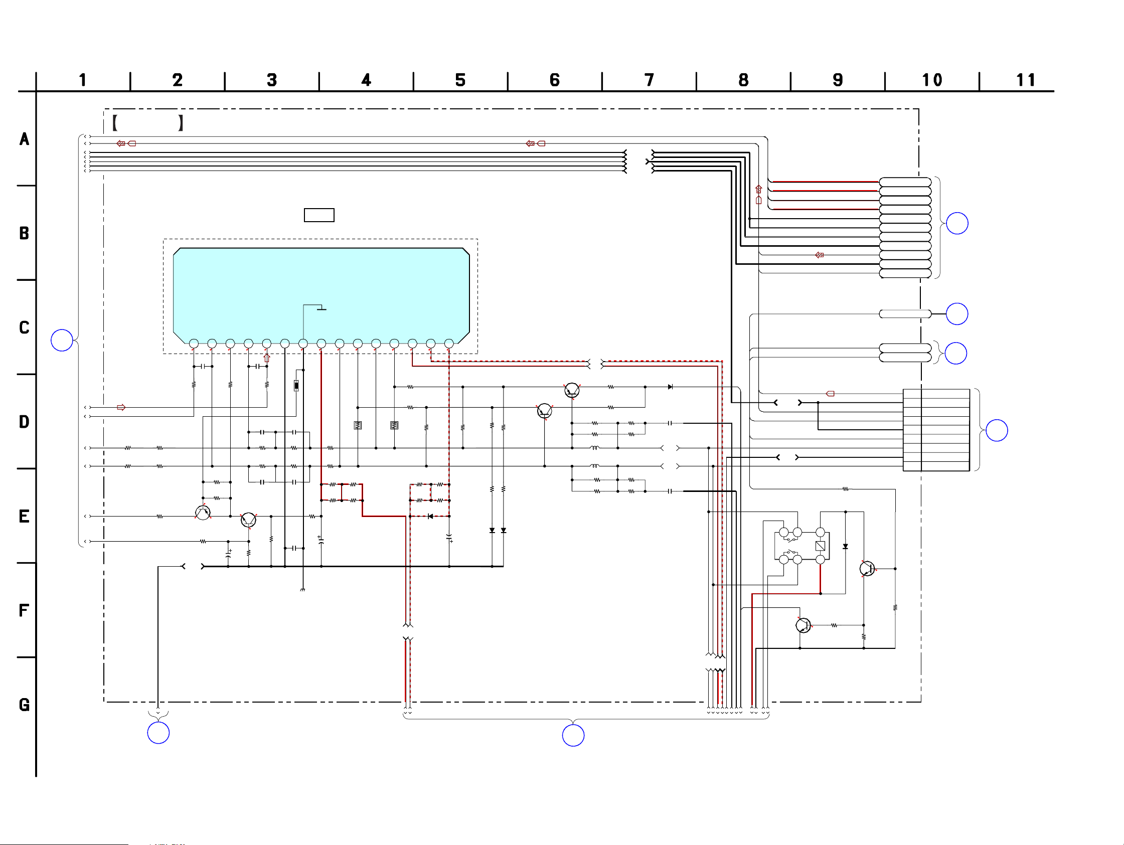
CX-LDB30/LDB50
7-10. SCHEMATIC DIAGRAM — MAIN SECTION (2/5) —
1
MAIN BOARD
(1/5)
(Page 33)
*5
*5
2SA1235TP-1EF
(2/5)
R41 4
Q406
P-GND
(R-IN)
IN-CH2
NF - CH2
00
C410
100p
50V
1k
R403
4.7k
R450
10k
2.1
0
2.3
THERMAL
DET
R452
22k
ST- BY
0.6
R449
4. 7k
2SC3052F-T1-LF
C426
22 25V
CD-P-GND
CD-D-GND
MP3GND
CD-A-GND
FUNC-GND
IC401
POWER AMP
IC401
STK403-120(LDB50)
STK403-090(LDB30)
0
C415
10p
R421
22k
R422
22k
C416
10p
C423
0. 1 25V
*3
C424,C425
50V:LDB30
63V:LDB50
SUB
SUB
47
100K
TH401
THERMI STOR
R455
10k
(R-OUT)
OUT- CH 2
OUT- CH 2
*6
R42 6
0. 22
0
OUT- CH 1
00
+PRE
0
R423
10k
R424
10k
R457 R459 R461 R463
10 10 10 10
*3
100
C424
(L-OUT)
D405
RE
-P
-VCC
123456789101112131415
-20
-47
*7
*7
R42 9
R462R460R458R456
10101010
*3
470
C425
OUT- C H1
+VCC
20
R427
1k
R428
1k
*6
R42 5
0. 22
R43 0
1N4002B
+VH
-VH
(L-IN)
NF - CH1
0
C409
100p
50V
C414
R419
R420
10p
C413
GND
IN-CH1
0
1k
R41 3
10p
22k
22k
Q407
2.3
22
MUTE
CONT
0
10k
R45 4
R453
220k
SHASSIS GND
*6
R426, R425
2W:LDB30
3W:LDB50
2SA1579T106-RR
R43 1
R43 2
4. 7k
10k
R433
R434
02
D40 3
D4
1SS355TE- 17
*7
R429, R430
470:LDB50
1k:LDB30
-VP
Q403
2SA1579T106-RR
Q404
DC DET
4. 7k
10k
1SS355TE- 17
0
0
0
0
0
OVERLOAD
0
R437
R439
L201
L202
R440
R438
DET
+VP
R435
10k
R436
10k
22
22
22
22
R441
R443
R444
R442
22
22
22
22
D401
1SS355TE-17
C417
0.1 50V
L CH
R CH
C418
0.1 50V
OVER-LOAD
CD-L
CD-R
AU-IN SW
RELAY ON
HP SW
AU-IN L
AU-IN R
AU-IN SW
HP SW
RELAY ON
7V
MP3VD
D-VDD
A-VDD
FUNC-GND
I-PRO
PROTECT
DET
A-GND
RY201
OSA-SS-212DM3
12V
34
56
3.3
R219
4.7k
1
D20 7
1SS355TE-1
2
Q208
2SC3052F-T1-LF1
0
R227
1k
9P JST 1.25MM
Q20 7
0.3
0
SWITCH
4. 7
R22 6
2SC30 52F- T1-LF
0.9
CD VM(7V)
MP3(3.3V)
DVDD(3.3V)
AVDD(3.3V)
MGND
MGND
D-GND
MP3GND
CD-L
CD-AGND
CD-R
AUDIO-IN SW
SP ON
HP SW
CN201
10k
R225
MAIN BOARD
(5/5)
5
(Page 37)
MAIN BOARD
(5/5)
6
(Page 37)
MAIN BOARD
(5/5)
7
(Page 37)
L-IN (AUDIO-IN)
9
GND (AUDIO-IN)
8
R-IN (AUDIO-IN)
7
SW (AUIDIO-IN)
6
GND
5
SW (HP)
4
HP-L
3
HP-GND
2
HP-R
1
D
JACK BOARD
CN203
(Page 30)
MAIN BOARD
30
29
28
27
26
25
24
R417
R418
*5
R415,R416
100:LDB30
470:LDB50
R415
*4
R416
*4
R451
1k
*4
R417,R418
470:LDB50
1k:LDB30
23
22
21
20
19
18
CX-LDB30/LDB50
31
10
MAIN BOARD(3/5)
(Page 35)
32 33
11
MAIN BOARD(4/5)
(Page 36)
3434
34
L- CH
35
+VP
R- CH
36 3738 39
-VP
NO MARK: FM
41
42
43 44
45
40
Page 35

7-11. SCHEMATIC DIAGRAM — MAIN SECTION (3/5) —
MAIN BOARD
(3/5)
1 2 3 4 5 6 8 7
2
MAIN BOARD
(1/5)
(Page 33)
1112 13
9
10
CX-LDB30/LDB50
14
15
16
17
E51
REG-IC BOARD
E
PT BOARD
CN002
(Page 41)
L CH
R CH
EH
MAIN BOARD
(5/5)
(Page 37)
W292
8
1 2
MAIN BOARD
(Page 37)
HEAD
(5/5)
+
–
–
+
–
+
3
REG-OUT
GND
REG-IN
CNA101
9
C137
VH(AC)
VL(AC)
GND(M)
VL(AC)
VH(AC)
AC-DET
VSTBY
P-ON
C303
0.001
50V
C304
0.001
50V
PB2
0. 1 25V
C324
CN302
7P PH
2.0MM
2134567
3
2
1
FR-GND
W293
3
REG-OUT
2
GND
1
REG-IN
8P
8
7
6
5
4
3
2
1
AC-DET
REC L
C319
10p 50V
PB L BIAS
PB R
REC R
C320
10p 50V
ERASE ERASE
*8
D101
G5SBA60L-6088: LDB50
GBJ4J10B9: LDB30
LDB30
470k
R10 1
470k
R103
LDB30
AC1
AC2
PB2
0
Q30 5
2SA1235TP-1EF
0
C321C322
1.4
47p 50V22p 50V
1.4
0
2SK2541-T
C307
470p 50V
C308
470p 50V
D101
*8
100k100k
R10 2R104
D102
GBJ4J10B9
47k
220k
R10 5
R106
47k
220k
R107
R10 8
PB L
R303
R308R30 9
100k
470k470k
JR301
R30 4
100k
PB R
1k
0
R30 7
Q306
1.1
REC/PB
SWITCH
2SA1235T P-1EF
Q309
2SK2541-T
0
Q308
2SK2541
0
Q307
1.4
R30 5
220k
0
0
R301
2.2k
R302
2.2k
*1
C101,C102
50V: LDB30
63V: LDB50
C105 C106
0.1
0.1
50V
50V
C107 C108
0.1
0.1
50V
50V
C109
0.1
50V
C110
0.1
50V
O-POWER
V-STBY V-STBY V-STBY
1.1
C101
2200
*1
C102
2200
*1
C103
4700
25V
C104
4700
25V
0
06
1k
R3
C301
470p
50V
C323
22p
50V
R311
1k
R312
1k
C604
0.1 16V B
220 10V
C602
Q313
RT1P141C-TP-1
SWITCH
D304
MC2840
T112-1
D301
MC2836
V
50
C310
001
0.
Q305-Q309
REC/PB
SWITCH
W701
1P
WIRE ASSY
TERMINAL,EARTH
SHASSIS GND
R313
R315
D602
UDZSTE-174.7B
4.6
1.3
4.5
R323
4.7k
R324
2. 2k
C364
47p
50V
CH
22k
47k
R316
47k
22k
R314
R155 R156
470 1/2W 470 1/2W
R157 R158
470 1/2W 470 1/2W
E
EP101
0
VDD
R110
10k
C114
470 25V
C318
0
VEE
REC L
REC R
WE R
V- STBY
O- PO
4. 7k
R10 9
Q101
0.6
2SC3052F-T1-LF
REPLAY DRIVE
D120 D121 D122
1N4002B 1N4002B 1N4002B
1k4. 7 k
R31 7R31 8
C30 2
C309
0.01
50V
C311
0.0022 50V
IC101
TA7812S
19.4
1 2
3
C115 C116
0.1
25V
L301
OSC BIAS
C312
0.001
50V
C363
0.1 16V
M
C313
0.022
50V
C314
0.01
50V
0. 01 50V
IC101
12V REG 7C REG
12
0.1
16V
C117
100 25V
31
-D-GND
FR-VDD
CD
CD- P- GND
FUNC-GND
TU9V
CD- A- GND
MP3GND
P- GND
TU-GND
FUNC-GND
Q311
KTA1266GR-AT
7
R319
0
22k
R31 0
0.3
0.3
Q3 10
2. 2
R32 0
KTC3 205 Y- AT
BIAS
OSC
0.3
D302
JW
C315
47 10V
7V
FR-GND
FUNC-GND
CD-D-GND
P-GND P-GND
A-GND A-GND
CD-P-GND
+VH
-VH
+VL +VL
-VL
470
R32 1
0.3
0.2
6.5
RT1N144C-
IC102
+VM
IC102
TA7807S
CD REG.
7
1 2
12
C11 8
3
0. 1 25V
C119
0. 1 16V
C12 0
SWITCH
100 16V
BIAS
D303
1SS355TE-17
Q312
TP-1
0.2
BIAS
SWITCH
7V
R111
470
73.3B
D10 5
UDZST E- 1
7V
R322
10k
220
16V
C325
BI AS
10
C317
O-
50V
O- BIAS
R117 R119
4.7 4.7
R159
2.2k
L-SPGL-SPG
R-SPGR-SPG
CD-P-GND
+VH
-VH
-VL
VDD REG
Q102
2SB1375
3.3
7
R112
47k
R113
100
C122
10 50V
3.6
6.4
2SC3052F-T1-LF
6.4
3
MC2840-T112-1
470
R11 4
Q103
VDD REG
D107
KTA1273-Y-AT
Q104
R115
47k
Q105
RT1N144C-TP-1
POWER
CONTROL
C123
100 16V
3.3
3.3
POWER
3
CONTROL
100
R11 6
0.3
KTC3198GR-A
11.1
9.7
22k
47k
R161
R160
CD-ON
1SS355TE-17
2.9
C12 4
Q106
0. 1 16V
I-PRO
D123
1SS355TE-17
8.9
VCC REG
V
C126
47 25
C121
100 16V
A-VDD
D108
VM
D- VDD
MP3 V D
C125
100 16V
MAIN BOARD
(Page 34)
46
47
48
49
50
51
52
53
54
55
56
57
58
10
(2/5)
12
MAIN BOARD
(4/5)
(Page 36)
NO MARK: FM
CX-LDB30/LDB50
3535
Page 36

CX-LDB30/LDB50
7-12. SCHEMATIC DIAGRAM — MAIN SECTION (4/5) —
MAIN BOARD
11
32
33 343536 3738394041 4243 4445
(2/5)
(Page 34)
MAIN BOARD
(3/5)
(Page 35)
12
46
47
48
49
50
51
52
53
54
55
56
57
58
MAIN BOARD
MC2838-T112-1
E51
1k
R135
D11 6
UDZS-TE17-12B
V-STBY
(4/5)
47k
R121
10k
R123
D110
D111
MC2838-T112-1
+VM +VM
k
47k
22
26
R1
10k
D112
MC2836
2. 2 50V
C129
D113 D115
MC2836 MC2836
2.7
R136
47 25V
D117
O- POWER
1SS355TE-17
2.7
Q111
0
D114
MC2838-T112-1
C130
22k
R12 5
10k
R131
R122
R124
2k
2. 2k
2.
28
R12 7
R1
7k
470
4.
4. 7 50V
30
R129
R1
C128
10k
47k
47k
R13 2
R13 4
R133
2
AC
AC1
+VH
-VH
2.2k
42.5
17.9
1k1k
R213R2 14
18.6
-18.8
-19.3
-42.7
4.7k
2.2k
1SS355TE-17
R203
470
Q203
2SC3052F-T1-LF
42.5
14.4
R228
47k
R207
10k
Q205
2SA1235TP-1EF
R229
4.7k
-14.4
-42.5
R204
470
A-GND
L-SPG
R-SPG
FAN-GND
+VM
14.4
R209R210
-14.4
2SA1235TP-1EF
4.7k
14.4
-14.4
R208
1k
D205
MC2838-T112-1
5TE-17
D203
10k10k
R21 1R212
1SS35
2k
2.
2k
2.
D204
1SS355TE- 17
Q204
D206
MC2836
R217
4.7k
L-CH
R-CH
R215
4.7k
+VP
A-GND
-VP
R216
4.7k
L-CH
R-CH
R218
4.7k
R231
R223
22k
R224
22k
R232
R222
100k
R221
DC- DET
100k
D209
LDB50
LDB50
R220
R201
42.5
R205
0
100k
LDB30
Q206
2SC3052F-T1-LF
R206
100k
0
-42.7
R202
R230
D210
1SS355TE-17
+VH
*2
C201
JW205
JW206
-VL
-VH
47
Q201
2SJ599-Z-E2-AZ
D201
*2
C202
47
RK46LF-T2
D211
RK36LF-B3
D212
RK36LF-B3
D202
RK46LF-T2
Q202
2SK3377-Z-E2-AZ
+VL
Q201,Q203,Q205
VP SWITCH
*2
C201, C202
50V: LDB30
63V: LDB50
Q202,Q204,Q206
–VP SWITCH
A-GND
L-SPG
R-SPG
FAN-GND
+VH
-VH
+VL
-VL
I-P RO
OVE R-L OAD
PROTECT
DET
ON DET
Q108
2SC3052F-T
RT1P141C-TP-1
052F-T1-LF
R139
1k
0
47k47k
R137R13 8
C131C13 2
0. 1 16V0.1 16V
R140
1k
DC-DET
PROTECT
100
2SA1235TP-1EF
R141
3.3 3.3
0
0
Q109
2SC3052F-T1-LF
PROTECT
DET
Q110
3.3
ET
DC- D
DET
22k
3.3
R14 2
-VP
+VP
L-CH
R- CH
L-SPG
C231
0.01 25V
R-SPG
SP- L
+VM
FAN-GND
SP- R
Q115
22k
R150
R151
KTC3198GR-A
12
12
12
Q114
2SC3052F-T1-LF
R152
4.7k
4.7k
1k
2. 22. 2
R153R154
100k
R149
2. 2k
12
12
12
12
13
Q1
2SC3052F-T
052F- T1-LF
Q112-Q115
FAN DRIVE
12
12
Q11 2
2SC3052F- T1-LF
0
R14 8
12
V
C135
47 25
TERMINAL, 4P SP
0. 01
C230 C229
0. 01
10k
R14 7
D118
MC2838-T112-1
0
R146
47k
R14 5
J201
50V
50V
0.001
SHASSIS GND
R143
100k
+
(L)
SPEAKER
+
(R)
C203
50V
10k
10k
R144
C133
4. 7 50V
CN291
3P
+B(FAN)
1
2
3
GND
NC
FAN
NO MARK: FM
CX-LDB30/LDB50
3636
Page 37

CX-LDB30/LDB50
7-13. SCHEMATIC DIAGRAM — MAIN SECTION (5/5) —
(5/5)
R910
M20
M18
M16
M14
M12
(7V)
M
CD V
CD VM(7V)
MGND
MGND
MP3(3.3V)
MP3GND
0.01 25V
C648
AVDD(3.3V)
CD-R
CD-AGND
CD-L
D-GND
DVDD(3.3V)
LED1
D1
R736
10k
K0
RC
R738
10k
K1
D2
E0
LED2
E1
D3
E2
D4
LED3
D5
47k
R911
R912
47k
47k
AU-IN
FR-VDD
5
MAIN
BOARD
(2/5)
(Page 34)
VDD1
KGND
FR-VDD
DISP_GND DISP_GND
CD VM(7V)
B
DRIVER
BOARD
CN701
(Page 30)
MAIN BOARD
(Page 34)
C
BD BOARD
CN201
(Page 28)
A
PANEL BOARD
CN502
(Page 39)
(2/5)
CNA702
SW2(CHUCK SW)
SW1(OUT SW)
SW3(TRIGGER SW)
M +V
FIN(POS)
RIN(NEG)
MGND
MP3(3.3V)
AVDD(3.3V)
DVDD(3.3V)
LED_STAND-BY
VDD1
LCD-SID
KEY0
RMC
KEY1
LCD-SIC
ENC0_VOL
LED_VOL
ENC1_BAS
LCD-RSTB
ENC2_TRE
KEY_GND
LCD-RS
LED_BKLIGHT
LCSB
FR-VDD(3.3V)
DISP_GND
+VM(7V)
6
M+7V
MGND
MGND
MP3STB
MP3REQ
MIACK
MICK
MIDIO
MDLP
MICS
MP3RST
MP3GND
SCOR
SENS
CLK
XLT
DATA
XRST
XTCN
ROUT
AGND
LOUT
DGND
DOUT
CN904
19P
7P
CN902
27P
MAIN BOARD
1
2
3
4
5
6
7
W702
1P
WIRE ASSY
TO W701
AUDIO-IN SW
27
26
25
24
23
22
21
20
19
18
17
16
15
14
13
12
11
10
9
8
7
R965
6
5
R966
4
3
2
1
19
18
17
16
15
14
13
12
11
10
9
8
7
6
5
4
3
2
1
MGND
C18
C17
C16
C15
C14
C13
C9
C8
C7
C6
C5
C4
C3
C2
C1
1k
1k
• See page 42 for Waveforms. • See page 45 for IC Pin Function Description.
CDM
MGND MGNDMGNDMGND
VDD1
FR-GNDFR-GND
0
81
0
R707
100
M14
82
0
R708
1k
M12
83
3.7
R709
1k
M16
84
3.7
R710
1k
M18
85
I-CDMSW1
0
R711
1k
M20
86
I-CDMSW2
0
87
NC
2.2
R715
1k
E0
E2
E1
A5
K1
K0
LED1
LED3
88
I-ENC0
3.7
R748
1k
89
I-HALFSW
2.3
R749
1k
90
I-ENC2 (TRE)
2.2
R750
1k
91
I-ENC1 (BAS)
0
92
NC
3.2
I-SUFFIX
93
3.7
R782
1k
94
I-ENDSW
3.2
R753
1k
I-KEY1
95
0
GND
96
3.2
R756
1k
97
I-KEY0
3.2
98
3.2
99
3.2
R920
100
100
R926
4.7k
FR-GND
VDD2
VDD1 VDD1
MAIN BOARD(3/5)
(Page 35)
*
220 (RU)
470 (E51)
0 (AEP)
C921
C917
220p 50V
0.0022 50V
HS
220p
RU, E51
4.7k
R993R994
1
*
1
C919
50V
C918
220p 50V
C913
0.001
C916
50V
0.0022 50V
C915
C937
0.0022 50V
C938
VDD1
C903
10 50V
0.1 16V
0.1 16V
VDD2
10k
R740
0.1 16V
RU, E51
.7k
10k
R741
4
R729
R2
C914
0.1
16V
NC
GND
NMI
I-RDSCLK
1.9
100
R773
R1
RU,
E51
C930
C1
C2
C6
AU-I N
100
100
100
100
1k
R78 4
R783
R785
R726
R730
3.2
3.2
0000000000000000
NC
VCC
O- XRST
O- XT ACN
I-RDSDATA
I-AUDIOIN
FUNC-CLK
I-MP3STBY
O-MILT
I-MP3REQ
I-MP3ACK
O- PLLCEI-TUNE
NC
NC
O- PLLDAT
AC- CUT
I-SCOR
3.4
47k
1k
100
100
100
R792
R703
R705
R754
R768
T1
10k
R723
AC-CUT
C931
0. 1 16V
100p 5 0V
C950
IC904
RESET
VDD1
C943
0.001
50V
T6
T7
100
R794
O-TUMUTE
I-CDMSW3
O- LCDATA
123456789101112 13 14 15 16 17 18 19 20 21 22 23 24 25 26 27 28 29 30
0
3.2 3.2 3.2
100
R96 3
D1
9
K0
0
NCNCNCNCNC
NC
NC
O- LCDSCK
I-RMC
O- VOLUMELED
00
1k
1k
100
R75 7
R724
R923
LED2
RC
C14
C905
22p 5 0V
Q
901
2SC3052F
T1-LF
RESET SWITCH
AC-DET
3.3
I-WAKEUPKYE
O-LDOUT
O-LDIN
VREF
AVCC
O-STBLED
P3DATA
O- MP3C LK
O- M
I-MP3DATA
0000
100
100
R746
R924
C15
C920
C922
100p 50V
100p 50V
3.2
3.4
BYTE
10k
R977
1.3 1.3
10k
R786
CNVSSRESE T
1k
R795
I-STEREO
100
R947
D2
CNVSS
0
22p 50V
C910
0
C923
F1
1k
R739
00
NC
NC
NC
NC
NC
NC
O- CDON
IC901
M30622MEP-
A26FPU0
IC901
SYSTEM CONTROL
34
ET
GND
32kHz-I N
0.001 50V
C926
VCC
32kHz-OUT
16MHz-OUT
16MHz-I N
I-RES
00000000
1.2
1.5
3.2 3.2
100
470k
16MHz
R995
32. 768KHz
R789
X902
C927
C909
X901
0.1
0.001
16V
50V
22p 50V
C911
0
0
470 10V
C929
JR902
C924
RESET
R979
47k
47k
D901
1SS355TE-17
R978
F3
470
R73 1
I-SENS
I-PLLDAT/I-STE
1k
R706
T5T3T4
0. 001 50V
C906
VDD2 VDD2
A1
A2
3.3
O- SOL
O- MOTOR
O- STK- PO
TXD
K
O- PLLCL
O- BKLI GHT
3
3.3 0
100
100
R76 7
R76 9
T2
10k
R980
D904
1SS355TE-17
IC904
PST3429UL
3
2
D5
A7
100
100
R776
R777
0002
515253545556575859606162636465666768697071727374757677787980
O- LC DCS
O-LCDCD
MP3RST
O-FRONTRELAY
O-LCD-RS
I-PROTECT
O-POWER
O- SCL
0
4.7k
4.7k
R788
R78 7
3.43.4
1
C933
FR-VDDFR-VDDFR-VDD
VDD1
VDD2
C912
0.001
50V
3.73
50
49
I-PLAYSWO- SDA
48
47
I-MICS
46
45
44
O-BIAS
43
O-PB2
42
41
I-HP
40
39
38
37
O-CLK
36
O-XTL
35
O-DAT
34
RTS
33
32
31
42
10k
R9
22 25V
3.2
3.2
3.2
3.2
3.2
0
0
0
3.1
0.6
0.2
3.2
3.2
3.2
3.2
3.3
0
0
3.3
0
TP996
#
TP997
#
Q906
2SC3052F-T1-LF
SWITCH
3.4
4
D90 8
1SS355TE-17
R962
R781
R714
R779
R780
R772
R771
R713
R770
R956
R955
R954
R958
R952
R953
FR-VDD
FR-GNDFR-GND
CL2
F1
MGN DMGN D
FR-VDDFR-VDD
100
CL2
C18
R949
100
C13
R950
100
R951
100
C9
100
D4
C8
R948
100
1k
1k
100
A8
1k
A6
100
D3
1k
F6
1k
F4
100
C5
100
C4
100
C3
100
100
C17
100
C16
R959
100
C7
D905
MC2836
4
10k
R941
C942
0.1
16V
C928
10
50V
GND
RESET
CNVSS
RXD
CLK
A4
A3
0.01 25V
C953
0.022
25V
R733
4.7k
R764
47k
C701
IC902
VDD REG
4
45
IC902
MM1614A
0
5.7
23
5.7
VCC
RTS
TXD
RTS
CLK
RXD
TXD
VDD2
FR-GNDFR-GND
100
R943
100
R945
1
100 16V
C941
C936
0.1
16V
CN901
1
GND
2
RESET
3
CNVSS
4
RXD
5
CLK1
6
VDD
7
RTS
8
TXD
100
R944
100
R946
R986
A1
RT1N144C-
A2
Q903
RT1N144C-
TP-1
T SOL DRIVE
0
Q902
TP-1
MOTOR
DRIVE
0
470
11.9
R988
470
0.7
D91 1
UDZSTE- 1710B
DI SP_ GND
V-STBY
FR-GND
DISP_GND
R913
470
R914
470
1k
R985
Q904
KTA1273Y-Y-AT
MOTOR DRIVE
1k
R987
Q905
KTA1273Y-Y-AT
T SOL DRIVE
Not used
11.9
0.3
D907
A5
+VM
11.9
11.9
R989
4.7k
R990
4.7k
R991
0.3
1SS355TE-17
4.7k
R763
4.7k
0
F3
F4
F6
R1
R2
T6
T7
T1
T2
T3
T4
T5
A3
A4
A8
+VM
FR-VDD
A6
MGND
HS
A7
FUNC-CLK
CD-ON
O-STK-POWER
O-POWER
I-PROTECT
RDS-CLK
RDS-DATA
STEREO
TU-MUTE
CE
PLL-CLK
DO
I-PULDAT/I-STE
TUNED
PB2
O-BIAS
V-STBY
FR-GND
VM
(12V)
FR-VDD(3.3V)
SP ON
HP SW
22k
10k
R791
R793
MGND
CN905
7P
7
END SW
6
GND
5
SOL
4
MOTOR
3
PACK
2
REC
1
PLAY SW
3
8
4
7
MAIN BOARD(1/5)
(Page 33)
MAIN BOARD(3/5)
(Page 35)
MAIN BOARD(1/5)
(Page 33)
MAIN BOARD(2/5)
(Page 34)
MECHANISM
TAPE
DECK
NO MARK: FM
CX-LDB30/LDB50
3737
Page 38

CX-LDB30/LDB50
7-14. PRINTED WIRING BOARD — PANEL BOARD —
PANEL BOARD
LCD 501
A
MAIN BOARD
JW505
CN502
19P
JW50 6
JW50 7
JW508
JW509
JW510
JW511
JW513
JW512
CN904
(Page 31)
JW501
JW502
JW503
JW504
IC501
D504
STANDBY
S511
I/1
S512
DISPLAY
LCD BACK LIGHT
D502 D503
JW514
• See page 24 for Circuit Boards Location. :Uses unleaded solder.
CD EJECT BOARD
TREBLE
W550
1-865-720-
S550
A
11
(11)
S513
i-Bass
W50 2
S503S502
BASS
JW5 17
JW51 6
JW51 5
VOLUME
D505
LDB50
R510
R511
R513
R512
R532
R529
C513
R530
R531
R537
R534
C514
R535
36
R5
R524
R525
Q502
LDB30
E
R
517
R522
R508
R507
06
C5
C908
C504
R526
R560
E
Q503
R554
R509
R504
D501
R505
R501
R502
R527
R528
C502
R518
R519
JR
R553
C503
C986
R516
C512
501
R521
C516
C517
TAPE
6
S50
PLAY MODE/
TUNING MODE
5
S50
DSYNC
516
S
CD
7
S50
x
4
S50
zREC/PAUSE/START
S515
TUNER
S93
TUNING –
6
AUDIO IN
TUNING +
. >
0
S51
FOLDER – FOLDER +
S929
S514
8
S50
S501
VOLUME
9
S50
W501
11
1-865-432-
(11)
R539
R540
C515R542
R541
R555
R556
R550
R551
R552
R557
R549
R558
R548
R547
R546
R559
1-865-432-
11
(11)
• Semiconductor
Location
Ref. No.
D501 B-9
D502 D-2
D503 D-3
D504 D-1
D505 D-5
IC501 C-2
Location
CX-LDB30/LDB50
Q502 D-7
Q503 D-9
3838
Page 39

7-15. SCHEMATIC DIAGRAM — PANEL BOARD —
D1
D5D2D4D3
CX-LDB30/LDB50
DISP_GND
PANEL BOARD
CD EJECT BOARD
S550
A
IC501
NJL24H400A
3.3
1
5
4
REMOTE CONTROL RECEIVER
2
3
IC501
C512
0.1
16V
3.3
B
2. 2k
R51 3
W550
2P
1
CD EJECT
2
KEY_GND
LCD
NC
2. 2k
2. 2k
2. 2k
2. 2k
R51 1
R51 2
CS
SI O
LCD501
110V
R50 9
R51 0
C506
56
891011
7
B
RS
CL
S
VSS
VDD
RESE T
LCD
110V
R508
V0
7
C908
R50
4
R50
22k
1234
NC
NC
D501
UDZSTE-175.1B
LCD BACK LIGHT
D502D503
SELU1910CXM-SSELU1910CXM-S
Q502
TP-1
D505
220
R525
2.4
R516
47k
R518
47
RC
VOLUME
LDB50
SELU6B14C-S-TP5
RT1N144C-
LED DRIVE
FR-VDD
L2
R524
470
Q503
2SC3052F-T1-LF
R522
1k
LED DRIVE
100k
R51 7
0.7
L3
470
R52 6R560
1.3
10k
D504
SLI-325URC
T31W
R527R528
1010
STANDBY
C504
R505
0. 01 25V
220
1k
470
FR-VDD
R501R502
C502
0. 01 25V B
+VM(7V)
4747
FR-VDD
C503
0. 01 25V B
L1
1k
R52 1
JR501
0
R51 9
0
VDD1
DISP_GND
0. 01 25V B
C986
D5
L3
D3
E2
D4
E1
L2
E0
D2
K1
RC
K0
D1
L1
19
18
17
16
15
14
13
12
11
10
9
8
7
6
5
4
3
2
1
CN502
19P
+VM(7V)
DISP_GND
FR-VDD(3.3V)
LCSB
LED_BKLIGHT
LCD-RS
KEY_GND
ENC2_TRE
LCD-RSTB
ENC1_BAS
LED_VOL
ENC0_VOL
LCD-SIC
KEY1
RMC
KEY0
LCD-SID
VDD1
LED_STAND-BY
A
MAIN BOARD
(5/5)
CN904
(Page 37)
CX-LDB30/LDB50
CD EJECT
KEY_GND
W502
R550
R552
47k
S510
TUNING – TUNING +
S516
CD SYNC
1
2
S509
R559
47k
zREC/REC PAUSE/START
S515
R551
22k
S508
AUDIO IN
S929
FOLDER –
10k
S936
TUNER
S514
FOLDER +
R549
4.7k
S507
CD
R556R557R558
4.7k10k22k
R548
2.2k
S506
TAPE
R555
2.2k
S513
i-Bass
R547
2.2k
S505
PLAY MODE/
TUNING MODE
S512
DISPLAY
R546
1k
S504
x
R553R554
1k2.2k
S511
I/1
K1
C516C517
0. 001 25V CH0. 001 25V CH
K0
KGND
E0
R54 1
4. 7k
10k
C 515
R542
0. 01 25V
KGND
S501
VOLUME BASS
E1
k
539
R
2. 2
R536R53 7
4. 7k10k
S502
1k
C 514
R54 0
0. 01 25V
E2
R53 4
2. 2k
R53 1
25V
C513
1
R53 2
1k
R53 5
0. 0
R529
S503
TREBLE
2. 2k
1k
R530
4. 7k
10k
NO MARK: FM
3939
Page 40

CX-LDB30/LDB50
7-16. PRINTED WIRING BOARD — PT BOARD —
PT BOARD
D005
D004
D007
D006
C005
E51
AEP, RU
PT003
AEP, RU
• See page 24 for Circuit Boards Location.
JW013
AEP, RU
JW016
JW006
JW007
JW021
E51
JW017
2P
CN001
JW022
JW014
JW015
PT0
04
JW005
:Uses unleaded solder.
JW018
E51
JW019
JW020
JW026
JW027
JW004
JW008
JW001
S
001
JW002
VOLT SELECTOR
AC IN
R003
C004
R00 2
D002
R004
R005
E
MAIN BOARD
CNA101
(Page 31)
JW025
AEP, RU
JW023
JW009
E51
PT001
CN002
JW024
E51
C003
JW011
E51
JW010
RY001
AEP, RU
JW028
RY002
JW029
JW030
002
C
3
JW00
1-865-433-
11
(11)
D001
R007
R008
11
1-865-433-
(11)
• Semiconductor
Location
Ref. No.
D001 D-7
D002 B-9
D004 B-1
D005 B-1
D006 B-1
D007 B-2
Location
CX-LDB30/LDB50
4040
Page 41

7-17. SCHEMATIC DIAGRAM — PT BOARD —
PT BOARD
PT001
MAIN PT 80W 230V
CX-LDB30/LDB50
E
MAIN BOARD
(3/5)
CNA101
(Page 35)
CN002
8P
VH(AC)
VL(AC)
GND(M)
VL(AC)
VH(AC)
AC-DET
VSTBY
P-ON
8
9
10
C004
0. 1 25V F
11
12
13
14
15
16
17
8
7
6
5
4
3
2
1
R005
100
D002
MC2838-T112-1
V
50
04
22k
R0
2
C005
2.
*
1
R007
22 : AEP, RU
0 : E51
*
2
R008
10 : AEP, RU
0 : E51
R002
R003
D006
1N4002B
D007
1N4002B
D004
1N4002B
D005
1N4002B
R007 R008
*
1
1k
1k
*
2
7
T.F
6
5
4
JW009
NEUTRAL
LIVE
CN001
2P
NEUTRAL
LIVE
2
1
W001
3
JW005
2
1
E51
JW011
W0 06
J
PT003
6
7
8
9
PT004
45
3
2
1
E51
JW010
3
C00
0.0022
JW008
W003
J
E51
E51
VOLT SELECTOR
S001
RY001
G5PA-1
E51
JW004
3
4
JW007
1
AEP, RU
2
C002
0.0022
E51
RY002
3 4
1
D001
1SS355TE-17
JW001
JW002
5 6
2
E51
45
6
3
7
8
9
2
1
AEP, RU
CX-LDB30/LDB50
NO MARK: FM
4141
Page 42

CX-LDB30/LDB50
•Waveforms
– BD Board –
– MAIN Board –
1
IC101 ra (RFACO)
200 mV/DIV, 1 µs/DIV
2
IC101 uj (XTAO)
59.1 ns (16.9 MHz)
1 V/DIV, 40 ns/DIV
• IC Block Diagrams
— BD Board —
28
PREVCC
1.2 Vp-p
3.3 Vp-p
OPOUT
27
OUTVREF
26
3
IC901 qg (16MHz-IN)
62.7 ns (16 MHz)
1 V/DIV, 40 ns/DIV
4
IC901 0 (32kHz-IN)
30.5 µs (32.768 kHz)
1 V/DIV, 20
VOLTAGE
REFERENCE
1
2
VIN
IC251 BA5947FM-E2
CH4CAPA
CH4IN
24
25
23
1.4 Vp-p
1.6 Vp-p
µ
s/DIV
IC303 BH15FB1WG
THERMAL
PROTECTION
OVER CURRENT
+
−
GND
CH3FIN
CH3RIN
22
PROTECTION
CONTROL
BLOCK
3NC4
STBY
GND
20
21
MUTING
MUTE
POWVCC
19
5
VOUT
CH3OUTF
18
CH3OUTR
17
D
CH4OUTF
16
D
CH4OUTR
15
DD
MIRR
DFCT
FOK
VSS
LOCK
MDP
SSTP
IOVSS1
SFDR
SRDR
TFDR
TRDR
FFDR
FRDR
IOVDD1
AVDD0
AVSS0
TEI
TEO
FEO
IC101 CXD3059AR
WFCK
C2PO
XPCK
SCOR
GFS
114
112
111
113
NC
119
120
INTERFACE
1
2
3
4
5
6
7
8
9
10
11
12
13
14
15
16
17
18
NC
19
E
20
F
21
22
23
FEI
24
25
VC
26
A
27
B
28
C
29
D
30
NC
MIRR
DFCT
FOK
PWM
GENERATOR
SERVO
DSP
A/D
CONVERTER
TE
VC
FE
SUM
118
SERVO
116
117
115
VDD
C4M
COUT
WDCK
XUGF
ATCK
110
109
108
DIGITAL
CLV
SCLK
107
SUB CODE
PROCESSOR
SENS
VDD
106
105
SERVO
AUTO
SEQUENCER
ERROR
CORRECTOR
XLAT
CLOK
104
CPU INTERFACE
VSS
DATA
101
103
102
D/A
INTERFACE
EFM
DEMODULATOR
SYSM
XRST
100
COVERTER
D/A
32k
RAM
EXCK
96
97
98
99
95
CLOCK
GENERATOR
DIGITAL OUT
SELECTOR
94
LPF
LPF
91
92NC93
90
RMUT
89
IOVDD0
88
NC
87
AVDD2
86
AOUT2
85
VREFR
84
AVSS2
83
AVSS1
82
VREFL
81
AOUT1
80
AVDD1
79
XVDD
78
XTAI
77
XTAO
76
XVSS
75
NC
74
IOVSS2
73
TES1
72
TEST
71
DOUT
70
IOVDD2
69
EMPHI
68
EMPH
67
VDD
66
BCK
65
PCMD
64
VSS
63
LRCK
LMUT
XTSL
IOVSS0
XTACN
SQSO
SQCK
SBSO
CX-LDB30/LDB50
+
–
INTERFACE
–
+
1
2
OPIN–
OPIN+
4
3
SW
CH1FIN
5
CH1RIN
INTERFACE
INTERFACE
6
CH2FIN
7
CH2RIN
ATT
LEVEL SHIFT
32
34
33
31
RFDCO
AVDD4
PDSENS
D
D
12
CH2OUTF
D D
13
CH1OUTR
14
CH1OUTF
VREF
10
POWVCC
11
CH2OUTR
9
8
GND
VREFIN
35
AC_SUM
APC
36LD37
EQ_IN
38NC40
PD
EQ
AMP
39
41
RFC
AVSS4
RFACO
ASYNMMETRY
CORRECTOR
42
43
44
RFACI
AVDD3
45
BIAS
ASYI
46
47
ASYO
48
VPCO
VCTL
49
50
AVSS3
DIGITAL
PLL
51
52
FILO
CLTV
FILI
DC/DC
CONVERTER
56
57
AVSS5
DDVRSEN
58
59
DDCR
NC
54
AVDD5
55
DDVROUT
53
PCO
62
LRCKI
61
PCMDI
60
BCKI
4242
Page 43

IC301 TC94A34FG-002
CX-LDB30/LDB50
VDDP
/RESET
STANDBY
/MICS
/MILP
MIDIO
/MICK
/MIACK/
AD16
VDDT
VSS
SDO0
MIMD
Generator
TEST
60
Timing
Decoder
Instruction
40 bit
round & limitround & limit
XI
59
PRAM
4k word
A0A1
MAC
A2A3
ALU
VDDX
XO
5762 5861 5663 52 50
VCO
x5
PROM
4k word
Control
Program
MXMYMZ
register
AXAY
VSSP
VCOI
64 55 53 51
1
2
3
4
5
6
7
8
9
10
11
MCU I/F
VSSX
CKO/
PO13/
AD16
Y0/Y1/Y2
XO/X1/X2
VDD
Y-Bus
VSS
54
1k bit
SRAM
X-Bus
PO0/
ERAM
register
X-Pointer
AD0
PO1/
XRAM
4k word
YRAM
4k word
4k wordx12k word
CRAM
4k word
CROM
4k word
AD1
SRAM I/F
x1
x9
PO2/
AD2
PO3/
AD3
PO4/
AD4
49
I/F
SRAM/DRAM
I/F
JTAG
48
47
46
45
44
43
42
41
40
39
38
PO5/AD5
PO6/AD6
PO7AD7
AD8
AD9
AD10
VDDT
SRMSTB
VDDM
PO8/AD11
PO9/AD12
BCKO
LRCKO
SDI0
BCKIA
LRCKIA
37
36
35
34
33
/CCE/
PO10/
AD13
BUCK/
PO11/
AD14
SDO3/
/OE
PO12/
AD15/
/CAS
SDO2/
/CS/
/RAS
Flag
PIO4/IO4
BUS2/FI2/
2sets
Address Calc.
PIO6/IO6
PIO5/IO5
BUS1/FI3/
General
Input/
Output
Port
BUS0/
PIO7/IO7
I/F
CDP
Control
SDO1//WE
IO3
PIO3/
register
Y-Pointer
register
C-Pointer
BUS3/FI1/
12
13
Audio I/F
14
15
16
Sub Code I/F
SDI1
DATA/
SBSY/
BCKIB
SFSY/
LRCKIB
DIT
TXO
Interrupt
VDD
Control
IRQ/FI0
CKI/CLCK/
VSS
Timer
PIO0/
SDI2/IO0
25 26 27 28 29 30 31 3217 18 19 20 21 22 23 24
PIO1/
SDI3/IO1
IO2
PIO2/
Bus
Switch
43
Page 44

CX-LDB30/LDB50
— MAIN Board —
IC601 BD3882FV
40
1
PB1N
— DRIVER Board —
REC1O39REC1N
2
PB1P3PB2P
REC2N37REC2O36INC235INC134INB233INB132INA231INA130RVFIL229RVFIL128OUT127OUT2
38
REAR
VOLUME
VOLUME
4
PB2N
5
FGND
6
PB2O
7
PB1O
FRONT
VOLUME
8
VOLIN19VOLIN2
FRONT
VOLUME
10
MGND
TREBLE
11
TRE1112TRE12
13
TRE21
BAS1225BAS1124BAS2223BAS2122MID1221MID11
26
BASS
BASS
REAR
MIDDLETREBLE
16
MID22
17
VDD
14
YRE2215MID21
MIDDLE
LOGIC
CONTROL
18SI19SC20
VEE
IC701 BA6956AN
TSD
CONTROL LOGIC
1 2 3 4 5 6 7 8 9
VREF
OUT2
RNF
OUT1
VM
VCC
FIN
GND
RIN
44
Page 45

• IC Pin Function Description
MAIN BOARD IC901 M30622MEP-A26FPU0 (SYSTEM CONTROLLER)
Pin No. Pin Name I/O Description
1 O-LCDATA O LCD DATA
2 O-LCDSCK O Data output to the fluorescent indicator tube
3 O-VOLUMELED O LED (i-Bass/DEMO) control signal output
4 I-RMC I Remote control signal input from the remote sensor
5 O-MP3DATA O MP3 DATA OUT
6 I-MP3DATA I MP3 DATA IN
7 O-MP3CLK O Clock output to the CD unit
8 BYTE I Destination setting input terminal
9 CNVSS I Flash data signal input terminal
10 32KHz-IN I Oscillation circuit signal input for the real time clock
11 32KHz-OUT I Oscillation circuit signal output for the real time clock
12 I-RESET — Reset signal input
13 16MHz-OUT — Oscillation circuit signal output for the system main clock
14 VSS — Ground terminal
15 16MHz-IN I Oscillation circuit signal input for the system main clock
16 VCC — Power supply terminal (+3.3 V)
17 NMI — HIGH always
18 I-RDSCLK I Clock signal input from the tuner
19 I-SCOR I Sub code sync signal input from the CD unit
20 AC-CUT I Power down detection signal input
21 NC — Not used
22 O-PLLCE O Latch signal output to the tuner
23 O-PLLDAT O Data output to the tuner
24 NC — Not used
25 I-PLLDAT/I-STEREO I Pll data or stereo tuner detection signal input terminal
26 I-TUNE I Tuner tuned status signal input from the tuner
27 O-PLLCLK O Clock output to the tuner
28 O-BKLIGHT O LED (BACK LIGHT) control signal output
29 O-SCL O 12C clock signal output
30 O-SDA O 12C data signal output
31 TXD — Flash link data output terminal
32 I-MP3ACK I Acknowledge signal input from the MP3 IC
33 I-MP3REQ I Request signal input from the MP3 IC
34 RTS O Flash RTS signal output terminal
35 O-DATA O Data output to the CD unit
36 O-XLT O Control data latch signal output to the CD unit
37 O-CLOCK O Clock output to the CD unit
38 O-POWER O Main power control signal output
39 I-PROTECT I Voltage detection signal input
40 O-LCDRESET O Clock signal output to the fluorescent indicator tube
41 I-HEADPHONE I Headphone signal input terminal
42 O-FRONTRELAY O Front relay on/off detection signal output
43 O-PB2 O Playback selection signal output for the tape deck
44 O-BIAS O Bias control signal output to the tape deck
45 O-MP3RST O Reset signal output to the MP3 IC
46 O-LCDCD O Latch signal output to the fluorescent indicator tube
47 I-MICS O Clock output to the MP3 IC
48 O-MILP O Latch pulse signal output to the MP3 IC
49 O-MP3STBY O Strobe signal output to the MP3 IC
CX-LDB30/LDB50
45
Page 46

CX-LDB30/LDB50
Pin No. Pin Name I/O Description
50 O-FUNCCLK O Clock output to the function IC (IC601)
51 I-PLAY SW I PLAY switch signal input from the tape deck
52 O-LCDCS O Chip select signal output to the fluorescent indicator tube
53 O-SOL O Solenoid control signal output to the tape deck
54 O-MOTOR O Motor control signal output to the tape deck
55 O-STKPOWER I/O STK POWER ON/OFF
56 I-SENS I SENS signal input from the CD unit
57 O-XTACN O Clock output from the CD unit
58 I-RDSDATA I RDS data input from the tuner
59 I-AUDION I Audio signal detection input terminal
60 O-XRST O Reset signal output to the CD unit
61 A9 — Not used
62 VCC — Power supply terminal
63 A8 — Not used
64 VSS — Ground terminal
65 O-CDON O CD power supply control signal output
66 A6 — Not used
67 A5 — Not used
68 A4 — Not used
69 A3 — Not used
70 A2 — Not used
71 A1 — Not used
72 A0 — Not used
73 D15/INT5 — Not used
74 I-WAKEUPKEY I System wake up signal input terminal in the standby status
75 D13/INT3 — Not used
76 D12 — Not used
77 D11 — Not used
78 D10 — Not used
79 I-STEREO O STEREO indicate signal from the Tuner unit
80 O-TUMUTE O Mute signal output to the Tuner unit
81 D7 — Not used
82 O-LDOUT O Loading motor control signal output
83 O-LDIN O Loading motor control signal output
84 I-CDMSW3 I CDM trigger switch input
85 I-CDMSW1 I CDM out switch input
86 I-CDMSW2 I CDM chack switch input
87 D1 I Not used
88 I-ENC0 I VOL signal input from the rotary encoder
89 I-HALFSW I Cassette half or rec switch detectin signal input
90 I-ENC2 I Treble signal input from the rotary encoder
91 I-ENC1 I Bass signal input from the rotary encoder
92 I-MODEL — Not used
93 I-SUFFIX I Version setting input terminal
94 I-END SW I END switch signal input from the tape deck
95 I-KEY1 I Key input 1
96 AVSS — Ground terminal
97 I-KEY0 I Key input 0
98 VREF — Reference voltage
99 AVCC — Power supply terminal
100 O-STLED O Standby LED control signal output (“L” : active)
46
Page 47

NOTE:
• -XX and -X mean standardized parts, so they
may have some difference from the original
one.
• Items marked “*” are not stocked since they
are seldom required for routine service.
Some delay should be anticipated when
ordering these items.
SECTION 8
EXPLODED VIEWS
• The mechanical parts with no reference
number in the exploded views are not supplied.
•Abbreviation
E51 : Chilean and Peruvian model.
RU : Russian model.
CX-LDB30/LDB50
Ver. 1.1
The components identified by mark 0 or
dotted line with mark 0 are critical for safety .
Replace only with part number specified.
8-1. PANEL SECTION
4
1
6
5
1
8
3
2
3
3
d
11
9
b
1
c
d
3
3
7
b
a
1
not
3
supplied
4
chassis
section
front panel section
4
1
4
Ref. No. Part No. Description Remark
1 4-242-531-01 QT2+3-10 W/O SLOT
2 3-254-146-01 SCREW (B3), (+) BV TAPPING
3 3-254-143-11 SCREW (B3), (+) BV TAPPING
4 3-254-143-01 SCREW (B3), (+) BV TAPPING
5 4-245-911-51 PANEL, TOP (LDB50)
5 4-245-911-61 PANEL, TOP (LDB30)
6 4-245-912-51 PANEL (L), SIDE (LDB50)
6 4-245-912-61 PANEL (L), SIDE (LDB30)
c
10
4
a
CD mechanism section
Ref. No. Part No. Description Remark
7 4-245-913-51 PANEL (R), SIDE (LDB50)
7 4-245-913-61 PANEL (R), SIDE (LDB30)
8 2-549-913-01 PANEL, BACK (AEP, UK, RU)
8 2-549-913-21 PANEL, BACK (E51)
9 1-763-697-21 DC FAN
10 1-828-403-11 WIRE (FLAT TYPE) (27 CORE)
11 2-595-983-01 CUSHION (PAENL SIDE)
47
Page 48

CX-LDB30/LDB50
Ver. 1.1
8-2. FRONT PANEL SECTION
55
52
53
57
51
54
58
56
59
62
64
61
65
74
63
66
71
77
75
80
76
67
b
a
68
b
69
a
82
80
83
81
70
81
not
supplied
80
81
79
73
72
not
supplied
not
supplied
78
60
Ref. No. Part No. Description Remark Ref. No. Part No. Description Remark
51 2-514-936-01 PANEL, CASSETTE (LDB50)
51 2-514-936-11 PANEL, CASSETTE (LDB30)
52 4-245-916-01 HOLDER, CASSETTE
53 4-246-745-01 CASSETTE, SPRING
54 4-245-938-01 SPRING (CASS), TORSION
55 2-514-938-01 WINDOW, DISP
56 2-514-944-01 KNOB, B/T
57 4-253-199-01 KNOB (VOL)
58 2-514-947-01 RING, VOL
59 2-514-959-01 HOLDER (VOL)
60 2-514-937-01 PANEL, CD
61 2-514-945-01 KEY, EJECT
62 2-514-935-01 CABINET, FRONT (LDB50: AEP)
62 2-514-935-11 CABINET, FRONT (LDB50: RU, E51)
62 2-514-935-21 CABINET, FRONT (LDB30: AEP, UK)
62 2-514-935-31 CABINET, FRONT (LDB30: RU, E51)
63 4-242-091-01 CUSHION
64 2-514-942-01 INDICATOR, POWER
65 2-548-151-01 CAP, POWER
66 2-514-939-01 KEY, POWER
67 X-2025-175-1 KEY ASSY, FUNC (A)
68 X-2025-176-1 KEY ASSY, FUNC (B)
69 2-514-946-01 KEY, REC
70 4-242-171-01 DAMPER 150 N
71 4-242-172-01 PLATE, LOCK
72 4-242-173-01 SPR-C, LOCK
73 4-242-175-01 HLDR, LOCK 2
74 4-253-764-01 COVER (CD)
75 A-1091-005-A PANEL BOARD, COMPLETE (LDB50)
75 A-1097-409-A PANEL BOARD, COMPLETE (LDB30)
76 A-1095-285-A CD EJECT BOARD, COMPLETE
77 1-828-360-11 WIRE (FLAT TYPE) (19 CORE)
78 A-1091-007-A JACK BOARD, COMPLETE
79 1-828-958-11 WIRE (FLAT TYPE) (9 CORE)
80 3-254-151-01 SCREW (B2.6), (+) P TAPPING
81 3-254-143-01 SCREW (B3), (+) BV TAPPING
82 1-828-945-11 WIRE (FLAT TYPE) (7 CORE)
83 1-796-352-41 DECK, MECHANICAL
48
Page 49

8-3. CHASSIS SECTION
CX-LDB30/LDB50
Ver. 1.1
102
102
101
not
supplied
103
104
103
102
102
not
supplied
103
102
108
107
109
not
supplied
105
106
PT001
106
110
not
supplied
111
112
102
not
supplied
Ref. No. Part No. Description Remark Ref. No. Part No. Description Remark
101 A-1091-001-A MAIN BOARD, COMPLETE (LDB50: AEP)
101 A-1091-956-A MAIN BOARD, COMPLETE (LDB30: AEP, UK)
101 A-1093-206-A MAIN BOARD, COMPLETE (LDB50: E51)
101 A-1093-223-A MAIN BOARD, COMPLETE (LDB50: RU)
101 A-1093-262-A MAIN BOARD, COMPLETE (LDB30: E51)
101 A-1093-269-A MAIN BOARD, COMPLETE (LDB30: RU)
102 3-254-143-01 SCREW (B3), (+) BV TAPPING
103 3-077-331-01 +BV3 (3-CR)
104 2-549-915-01 HEAT SINK (MAIN)
105 A-1091-003-A PT BOARD, COMPLETE (AEP, UK, RU)
105 A-1093-208-A PT BOARD, COMPLETE (E51)
106 4-900-386-01 SCREW
107 3-254-142-01 SCREW (B3), (+) BV TAPPING
108 1-828-967-11 WIRE (FLAT TYPE) (11 CORE) (RU, E51)
108 1-828-987-11 WIRE (FLAT TYPE) (15 CORE) (AEP, UK)
109 1-693-626-11 TUNER (FM/AM) (AEP, UK)
109 1-693-628-21 TUNER (FM/AM) (E51)
109 1-693-629-31 TUNER (FM/AM) (RU)
110 1-400-285-11 F-BEAD, E2515MRT
111 3-703-244-00 BUSHING (2104), CORD
0 112 1-769-744-81 CORD, POWER (UK)
0 112 1-830-188-11 CORD, POWER (AEP, RU)
0 PT001 1-443-216-11 TRANSFORMER, POWER (LDB50: AEP, RU)
0 PT001 1-443-217-11 TRANSFORMER, POWER (LDB30: AEP, UK, RU)
0 PT001 1-443-218-11 TRANSFORMER, POWER (LDB50: E51)
0 PT001 1-443-220-11 TRANSFORMER, POWER (LDB30: E51)
The components identified by mark 0 or dotted
line with mark 0 are critical for safety.
Replace only with part number specified.
49
Page 50

CX-LDB30/LDB50
8-4. CD MECHANISM DECK SECTION 1 (CDM80BV-F4BD81)
160
155
157
156
#5
151
160
158
159
A
160
M701
161
160
162
B
151
B
154
153
A
152
163
151
Ref. No. Part No. Description Remark Ref. No. Part No. Description Remark
151 4-985-672-01 SCREW (+PTPWHM2.6), FLOATING
152 2-515-538-01 SPRING (HOLDER DOWN B), COIL
153 4-245-653-01 BELT (MOT)
154 4-245-662-02 PULLEY (GEAR)
155 4-245-646-01 GEAR (IDL-F)
156 4-245-644-01 GEAR (IDL-D)
157 4-245-645-01 GEAR (IDL-E)
158 4-246-203-01 LEVER (RELEASE)
159 4-245-630-01 LEVER (SW)
160 4-951-620-01 SCREW (2.6X8), +BVTP
161 4-245-639-01 LEVER (CL UP2)
162 1-688-337-11 DRIVER BOARD
163 7-623-921-01 RING, RETAINING, CAPSTAN
M701 X-4955-496-1 MOTOR (PULLEY) ASSY (LOADING)
#5 7-685-106-19 SCREW +P 2X10 TYPE2 NON-SLIT
50
Page 51

8-5. CD MECHANISM DECK SECTION 2 (CDM80BV-F4BD81)
212
211
CX-LDB30/LDB50
214
213
210
215
209
208
216
207
218
217
205
206
206
205
204
not
supplied
219
203
220
202
201
203
202
201
Ref. No. Part No. Description Remark Ref. No. Part No. Description Remark
201 4-245-627-01 WASHER (6-2.7-0.4)
202 4-245-637-01 ROLLER, RUBBER
203 4-245-649-01 GEAR (IDL-I)
204 4-245-657-01 LEVER (LOADING-R)
205 4-245-647-01 GEAR (IDL-G)
206 4-245-648-01 GEAR (IDL-H)
207 4-245-655-01 CHASSIS (TOP)
208 2-103-179-01 SPRING (LOADING RV), TORSION
209 4-245-650-01 GEAR (IDL-J)
210 4-245-651-01 GEAR (IDL-L)
211 4-245-640-01 GEAR (CAP)
212 4-251-780-01 CAP (CLAMP 215V)
213 4-245-638-01 LEVER (CL UP1)
214 4-985-672-01 SCREW (+PTPWHM2.6), FLOATING
215 4-245-636-01 SPR-T (CL DOWN)
216 4-245-658-01 LEVER (DISC STOP)
217 4-245-659-01 LEVER (DISC SENSOR)
218 2-103-178-01 SPRING (LOADING LV), TORSION
219 X-4956-149-1 CLAMPER (215V) ASSY
220 4-245-656-01 LEVER (LOADING-L)
51
Page 52

CX-LDB30/LDB50
d
8-6. CD MECHANISM DECK SECTION 3 (CDM80BV-F4BD81)
259
258
257
256
260
261
262
253
265
255
not
supplied
251
254
259
264
252
263
not
supplie
Ref. No. Part No. Description Remark Ref. No. Part No. Description Remark
251 4-245-643-01 GEAR (IDL-C)
252 4-245-644-01 GEAR (IDL-D)
253 2-515-536-01 SPRING (DIR), TENSION COIL
254 4-245-642-01 GEAR (IDL-B)
255 4-245-814-01 LEVER (DIR FIRST)
256 2-515-534-01 SPRING (DIR BACK), TENSION COIL
257 4-245-660-01 LEVER (DIR)
258 4-245-641-01 GEAR (IDL-A)
259 4-245-640-01 GEAR (CAP)
260 4-245-628-01 LEVER (BU LOCK)
261 4-248-206-01 WASHER (3-1-0.4)
262 4-245-624-01 LEVER, CLOSE
263 4-245-635-01 SPR-E (CLOSE LEVER)
264 4-245-629-01 GEAR (BU LOCK)
265 X-2021-531-1 CHASSIS (BOTTOM) ASSY
52
Page 53

8-7. BASE UNIT SECTION
306
305
CX-LDB30/LDB50
307
304
301
303
304
303
304
303
304
S101
308
302
309
Ref. No. Part No. Description Remark Ref. No. Part No. Description Remark
0 301 8-820-252-01 OPTICAL PICK-UP (KSM-215CFP)
(including M101,M102)
302 A-4751-434-A BD BOARD, COMPLETE
303 4-985-672-01 SCREW (+PTPWHM2.6), FLOATING
304 4-992-054-11 RUBBER, VIBRATION PROOF
305 X-4956-148-1 HOLDER (BU215V) ASSY
306 4-216-085-01 SPRING (F-1), TENSION
307 4-216-086-01 SPRING (F-2), TENSION
308 1-827-992-11 WIRE (FLAT TYPE) (16 CORE)
309 2-629-303-01 PLATE (SHIELD BD)
S101 1-771-853-11 SWITCH, DETECTION (LIMIT)
The components identified by mark 0 or dotted
line with mark 0 are critical for safety.
Replace only with part number specified.
53
Page 54

CX-LDB30/LDB50
SECTION 9
BD
NOTE:
• Due to standardization, replacements in the
parts list may be different from the parts
specified in the diagrams or the components
used on the set.
• -XX and -X mean standardized parts, so they
may have some difference from the original
one.
• Items marked “*” are not stocked since they
are seldom required for routine service.
Some delay should be anticipated when
ordering these items.
• CAPACITORS
uF: µF
Ref. No. Part No. Description Remark Ref. No. Part No. Description Remark
A-4751-434-A BD BOARD, COMPLETE
*******************
< CAPACITOR >
C10 1-165-989-11 CERAMIC CHIP 10uF 10% 6.3V
C11 1-165-989-11 CERAMIC CHIP 10uF 10% 6.3V
C14 1-164-360-11 CERAMIC CHIP 0.1uF 16V
C15 1-164-360-11 CERAMIC CHIP 0.1uF 16V
C16 1-115-156-11 CERAMIC CHIP 1uF 10V
C17 1-126-246-11 ELECT CHIP 220uF 20% 4V
C18 1-162-964-11 CERAMIC CHIP 0.001uF 10% 50V
C111 1-162-967-11 CERAMIC CHIP 0.0033uF 10% 50V
C112 1-164-315-11 CERAMIC CHIP 470PF 5% 50V
C113 1-162-967-11 CERAMIC CHIP 0.0033uF 10% 50V
C114 1-164-315-11 CERAMIC CHIP 470PF 5% 50V
C115 1-164-360-11 CERAMIC CHIP 0.1uF 16V
C116 1-128-995-21 ELECT CHIP 100uF 20% 10V
C122 1-107-826-11 CERAMIC CHIP 0.1uF 10% 16V
C123 1-107-826-11 CERAMIC CHIP 0.1uF 10% 16V
C124 1-162-959-11 CERAMIC CHIP 330PF 5% 50V
C125 1-164-360-11 CERAMIC CHIP 0.1uF 16V
C131 1-162-927-11 CERAMIC CHIP 100PF 5% 50V
C132 1-117-863-11 CERAMIC CHIP 0.47uF 10% 6.3V
C133 1-162-970-11 CERAMIC CHIP 0.01uF 10% 25V
C134 1-164-360-11 CERAMIC CHIP 0.1uF 16V
C141 1-107-826-11 CERAMIC CHIP 0.1uF 10% 16V
C142 1-162-965-11 CERAMIC CHIP 0.0015uF 10% 50V
C143 1-164-360-11 CERAMIC CHIP 0.1uF 16V
C151 1-128-995-21 ELECT CHIP 100uF 20% 10V
C161 1-164-360-11 CERAMIC CHIP 0.1uF 16V
C162 1-164-360-11 CERAMIC CHIP 0.1uF 16V
C163 1-164-360-11 CERAMIC CHIP 0.1uF 16V
C171 1-162-919-11 CERAMIC CHIP 22PF 5% 50V
C172 1-162-920-11 CERAMIC CHIP 27PF 5% 50V
C174 1-164-360-11 CERAMIC CHIP 0.1uF 16V
C181 1-164-360-11 CERAMIC CHIP 0.1uF 16V
C182 1-164-360-11 CERAMIC CHIP 0.1uF 16V
C183 1-124-778-00 ELECT CHIP 22uF 20% 6.3V
C184 1-124-778-00 ELECT CHIP 22uF 20% 6.3V
ELECTRICAL PARTS LIST
• COILS
uH: µH
• RESISTORS
All resistors are in ohms.
METAL: Metal-film resistor.
METAL OXIDE: Metal oxide-film resistor.
F: nonflammable
•Abbreviation
E51 : Chilean and Peruvian model.
RU : Russian model.
C201 1-128-995-21 ELECT CHIP 100uF 20% 10V
C203 1-128-995-21 ELECT CHIP 100uF 20% 10V
C209 1-162-970-11 CERAMIC CHIP 0.01uF 10% 25V
C210 1-107-826-11 CERAMIC CHIP 0.1uF 10% 16V
C211 1-164-230-11 CERAMIC CHIP 220PF 5% 50V
C212 1-162-919-11 CERAMIC CHIP 22PF 5% 50V
C213 1-162-919-11 CERAMIC CHIP 22PF 5% 50V
C251 1-162-969-11 CERAMIC CHIP 0.0068uF 10% 25V
C252 1-164-360-11 CERAMIC CHIP 0.1uF 16V
C255 1-164-360-11 CERAMIC CHIP 0.1uF 16V
C257 1-164-360-11 CERAMIC CHIP 0.1uF 16V
C258 1-164-360-11 CERAMIC CHIP 0.1uF 16V
C259 1-164-360-11 CERAMIC CHIP 0.1uF 16V
C260 1-128-394-11 ELECT CHIP 220uF 20% 10V
C302 1-164-360-11 CERAMIC CHIP 0.1uF 16V
C303 1-164-360-11 CERAMIC CHIP 0.1uF 16V
C305 1-126-246-11 ELECT CHIP 220uF 20% 4V
C306 1-164-360-11 CERAMIC CHIP 0.1uF 16V
C307 1-164-360-11 CERAMIC CHIP 0.1uF 16V
C308 1-126-208-21 ELECT CHIP 47uF 20% 4V
C309 1-164-360-11 CERAMIC CHIP 0.1uF 16V
C310 1-164-360-11 CERAMIC CHIP 0.1uF 16V
C311 1-164-360-11 CERAMIC CHIP 0.1uF 16V
C312 1-164-360-11 CERAMIC CHIP 0.1uF 16V
C313 1-164-360-11 CERAMIC CHIP 0.1uF 16V
C314 1-126-208-21 ELECT CHIP 47uF 20% 4V
C315 1-107-826-11 CERAMIC CHIP 0.1uF 10% 16V
C316 1-162-966-11 CERAMIC CHIP 0.0022uF 10% 50V
C317 1-162-970-11 CERAMIC CHIP 0.01uF 10% 25V
C318 1-162-970-11 CERAMIC CHIP 0.01uF 10% 25V
C320 1-216-864-11 SHORT CHIP 0
CN101 1-770-425-11 CONNECTOR, FFC/FPC 16P
CN201 1-818-350-11 CONNECTOR (FFC) 27P
FB301 1-500-445-21 FERRITE, EMI (SMD)(2012)
• SEMICONDUCTORS
In each case, u: µ, for example:
uA. . : µA. . , uPA. . , µPA. . ,
uPB. . : µPB. . , uPC. . , µPC. . ,
uPD. . : µPD. .
When indicating parts by reference number,
please include the board name.
The components identified by mark 0 or
dotted line with mark 0 are critical for safety.
Replace only with part number specified.
< CONNECTOR >
< FERRITE BEAD >
C185 1-164-315-11 CERAMIC CHIP 470PF 5% 50V
C186 1-164-315-11 CERAMIC CHIP 470PF 5% 50V
C194 1-164-360-11 CERAMIC CHIP 0.1uF 16V
C195 1-164-360-11 CERAMIC CHIP 0.1uF 16V
C196 1-164-360-11 CERAMIC CHIP 0.1uF 16V
54
< IC >
IC101 8-752-425-12 IC CXD3059AR
IC251 6-705-808-01 IC BA5947FM-E2
IC301 6-705-365-01 IC TC94A34FG-002
IC303 6-705-807-01 IC BH15FB1WG
Page 55

CX-LDB30/LDB50
CD EJECT JACKBD DRIVER
Ref. No. Part No. Description Remark Ref. No. Part No. Description Remark
< TRANSISTOR >
Q10 6-551-120-01 TRANSISTOR 2SA2119K
< RESISTOR >
R410 1-216-809-11 METAL CHIP 100 5% 1/10W
R411 1-216-809-11 METAL CHIP 100 5% 1/10W
R412 1-216-809-11 METAL CHIP 100 5% 1/10W
R419 1-216-809-11 METAL CHIP 100 5% 1/10W
R10 1-216-791-11 METAL CHIP 3.3 5% 1/10W
R11 1-216-864-11 SHORT CHIP 0
R12 1-216-845-11 METAL CHIP 100K 5% 1/10W
R13 1-218-446-11 METAL CHIP 1 5% 1/10W
R111 1-216-821-11 METAL CHIP 1K 5% 1/10W
R112 1-216-835-11 METAL CHIP 15K 5% 1/10W
R113 1-216-821-11 METAL CHIP 1K 5% 1/10W
R114 1-216-835-11 METAL CHIP 15K 5% 1/10W
R121 1-216-835-11 METAL CHIP 15K 5% 1/10W
R131 1-216-857-11 METAL CHIP 1M 5% 1/10W
R132 1-216-833-11 METAL CHIP 10K 5% 1/10W
R133 1-216-848-11 METAL CHIP 180K 5% 1/10W
R141 1-216-829-11 METAL CHIP 4.7K 5% 1/10W
R142 1-216-821-11 METAL CHIP 1K 5% 1/10W
R143 1-216-827-11 METAL CHIP 3.3K 5% 1/10W
R151 1-216-864-11 SHORT CHIP 0
R161 1-216-809-11 METAL CHIP 100 5% 1/10W
R162 1-216-841-11 METAL CHIP 47K 5% 1/10W
R163 1-216-809-11 METAL CHIP 100 5% 1/10W
R165 1-216-864-11 SHORT CHIP 0
R171 1-216-817-11 METAL CHIP 470 5% 1/10W
R172 1-216-857-11 METAL CHIP 1M 5% 1/10W
R173 1-216-295-91 SHORT CHIP 0
R181 1-216-809-11 METAL CHIP 100 5% 1/10W
R182 1-216-809-11 METAL CHIP 100 5% 1/10W
R191 1-216-864-11 SHORT CHIP 0
R201 1-500-445-21 FERRITE, EMI (SMD)(2012)
R203 1-216-864-11 SHORT CHIP 0
R204 1-500-445-21 FERRITE, EMI (SMD)(2012)
R205 1-216-864-11 SHORT CHIP 0
R251 1-216-833-11 METAL CHIP 10K 5% 1/10W
R252 1-216-837-11 METAL CHIP 22K 5% 1/10W
R253 1-216-833-11 METAL CHIP 10K 5% 1/10W
R301 1-216-845-11 METAL CHIP 100K 5% 1/10W
R302 1-216-833-11 METAL CHIP 10K 5% 1/10W
R303 1-216-845-11 METAL CHIP 100K 5% 1/10W
R305 1-216-845-11 METAL CHIP 100K 5% 1/10W
R306 1-216-864-11 SHORT CHIP 0
R307 1-216-833-11 METAL CHIP 10K 5% 1/10W
R313 1-216-813-11 METAL CHIP 220 5% 1/10W
< VIBRATOR >
X171 1-767-408-21 VIBRATOR, CRYSTAL 16.934MHz
************************************************************
A-1095-285-A CD EJECT BOARD, COMPLETE
************************
< SWITCH >
S550 1-762-875-21 SWITCH, KEYBOARD (Z)
************************************************************
1-688-337-11 DRIVER BOARD
*************
< CAPACITOR >
C705 1-162-306-11 CERAMIC 0.01uF 30% 16V
C711 1-126-964-11 ELECT 10uF 20% 50V
< CONNECTOR >
CN701 1-785-333-11 PIN, CONNECTOR (LIGHT ANGLE) 7P
< DIODE >
D701 8-719-921-40 DIODE MTZJ-T-77-4.7C
< IC >
IC701 8-759-598-69 IC BA6956AN
< RESISTOR >
R701 1-249-415-11 CARBON 680 5% 1/4W
R702 1-247-807-31 CARBON 100 5% 1/4W
< SWITCH >
S701 1-762-951-21 SWITCH, PUSH (DISC IN/OUT)
S702 1-762-951-21 SWITCH, PUSH (CHUKING)
S703 1-762-951-21 SWITCH, PUSH (TRIGGER)
************************************************************
A-1091-007-A JACK BOARD, COMPLETE
*********************
R351 1-216-809-11 METAL CHIP 100 5% 1/10W
R352 1-216-809-11 METAL CHIP 100 5% 1/10W
R353 1-216-809-11 METAL CHIP 100 5% 1/10W
R354 1-216-809-11 METAL CHIP 100 5% 1/10W
R401 1-216-809-11 METAL CHIP 100 5% 1/10W
R402 1-216-809-11 METAL CHIP 100 5% 1/10W
R403 1-216-809-11 METAL CHIP 100 5% 1/10W
R404 1-216-809-11 METAL CHIP 100 5% 1/10W
R405 1-216-809-11 METAL CHIP 100 5% 1/10W
R406 1-216-809-11 METAL CHIP 100 5% 1/10W
R407 1-216-809-11 METAL CHIP 100 5% 1/10W
R408 1-216-809-11 METAL CHIP 100 5% 1/10W
R409 1-216-809-11 METAL CHIP 100 5% 1/10W
< CAPACITOR >
C291 1-162-927-11 CERAMIC CHIP 100PF 5% 50V
C292 1-162-927-11 CERAMIC CHIP 100PF 5% 50V
C293 1-126-960-11 ELECT 1uF 20% 50V
C294 1-126-960-11 ELECT 1uF 20% 50V
C295 1-162-927-11 CERAMIC CHIP 100PF 5% 50V
C299 1-162-927-11 CERAMIC CHIP 100PF 5% 50V
< CONNECTOR >
CN203 1-568-828-11 CONNECTOR, FFC 9P
55
Page 56

CX-LDB30/LDB50
Ver. 1.1
MAINJACK
Ref. No. Part No. Description Remark Ref. No. Part No. Description Remark
< JACK >
J291 1-815-629-11 JACK (AUDIO IN)
J292 1-815-629-11 JACK (PHONES)
< RESISTOR >
R191 1-215-867-00 METAL OXIDE 470 5% 1W
R285 1-216-825-11 METAL CHIP 2.2K 5% 1/10W
R286 1-216-825-11 METAL CHIP 2.2K 5% 1/10W
R289 1-216-809-11 METAL CHIP 100 5% 1/10W
R290 1-216-809-11 METAL CHIP 100 5% 1/10W
C130 1-126-947-11 ELECT 47uF 20% 25V
C131 1-107-826-11 CERAMIC CHIP 0.1uF 10% 16V
C132 1-107-826-11 CERAMIC CHIP 0.1uF 10% 16V
C133 1-126-963-11 ELECT 4.7uF 20% 50V
C135 1-126-947-11 ELECT 47uF 20% 25V
C201 1-126-967-11 ELECT 47uF 20% 50V
(LDB30)
C201 1-128-552-51 ELECT 47uF 20% 63V
(LDB50)
C202 1-126-967-11 ELECT 47uF 20% 50V
(LDB30)
R292 1-215-867-00 METAL OXIDE 470 5% 1W
R293 1-216-825-11 METAL CHIP 2.2K 5% 1/10W
R294 1-216-825-11 METAL CHIP 2.2K 5% 1/10W
R295 1-216-825-11 METAL CHIP 2.2K 5% 1/10W
R296 1-216-825-11 METAL CHIP 2.2K 5% 1/10W
************************************************************
A-1091-001-A MAIN BOARD, COMPLETE (LDB50: AEP)
A-1091-956-A MAIN BOARD, COMPLETE (LDB30: AEP, UK)
A-1093-206-A MAIN BOARD, COMPLETE (LDB50: E51)
A-1093-223-A MAIN BOARD, COMPLETE (LDB50: RU)
A-1093-262-A MAIN BOARD, COMPLETE (LDB30: E51)
A-1093-269-A MAIN BOARD, COMPLETE (LDB30: RU)
*********************
4-253-763-01 SHEET (LCD)
< CAPACITOR >
C101 1-128-550-11 ELECT 2200uF 20% 50V
(LDB30)
C101 1-135-632-61 ELECT 2200uF 20% 63V
(LDB50)
C102 1-128-550-11 ELECT 2200uF 20% 50V
(LDB30)
C102 1-135-632-61 ELECT 2200uF 20% 63V
(LDB50)
C103 1-128-548-11 ELECT 4700uF 20% 25V
C104 1-128-548-11 ELECT 4700uF 20% 25V
C105 1-127-888-51 CERAMIC 0.1uF 10% 50V
C106 1-127-888-51 CERAMIC 0.1uF 10% 50V
C107 1-127-888-51 CERAMIC 0.1uF 10% 50V
C108 1-127-888-51 CERAMIC 0.1uF 10% 50V
C109 1-127-888-51 CERAMIC 0.1uF 10% 50V
C110 1-127-888-51 CERAMIC 0.1uF 10% 50V
C114 1-126-941-11 ELECT 470uF 20% 25V
C115 1-164-156-11 CERAMIC CHIP 0.1uF 25V
C116 1-107-826-11 CERAMIC CHIP 0.1uF 10% 16V
C117 1-104-665-11 ELECT 100uF 20% 25V
C118 1-164-156-11 CERAMIC CHIP 0.1uF 25V
C119 1-107-826-11 CERAMIC CHIP 0.1uF 10% 16V
C120 1-126-933-11 ELECT 100uF 20% 16V
C121 1-126-933-11 ELECT 100uF 20% 16V
C122 1-126-964-11 ELECT 10uF 20% 50V
C123 1-126-933-11 ELECT 100uF 20% 16V
C124 1-107-826-11 CERAMIC CHIP 0.1uF 10% 16V
C125 1-126-933-11 ELECT 100uF 20% 16V
C126 1-126-947-11 ELECT 47uF 20% 25V
C128 1-126-963-11 ELECT 4.7uF 20% 50V
C129 1-126-961-11 ELECT 2.2uF 20% 50V
C202 1-128-552-51 ELECT 47uF 20% 63V
(LDB50)
C203 1-162-964-11 CERAMIC CHIP 0.001uF 10% 50V
C229 1-162-974-11 CERAMIC CHIP 0.01uF 50V
C230 1-162-974-11 CERAMIC CHIP 0.01uF 50V
C231 1-162-970-11 CERAMIC CHIP 0.01uF 10% 25V
C301 1-164-315-11 CERAMIC CHIP 470PF 5% 50V
C302 1-130-483-00 MYLAR 0.01uF 5% 50V
C303 1-162-964-11 CERAMIC CHIP 0.001uF 10% 50V
C304 1-162-964-11 CERAMIC CHIP 0.001uF 10% 50V
C307 1-164-315-11 CERAMIC CHIP 470PF 5% 50V
C308 1-164-315-11 CERAMIC CHIP 470PF 5% 50V
C309 1-130-483-00 MYLAR 0.01uF 5% 50V
C310 1-162-964-11 CERAMIC CHIP 0.001uF 10% 50V
C311 1-130-475-00 MYLAR 0.0022uF 5% 50V
C312 1-130-471-00 MYLAR 0.001uF 5% 50V
C313 1-130-487-00 MYLAR 0.022uF 5% 50V
C314 1-130-483-00 MYLAR 0.01uF 5% 50V
C315 1-126-947-11 ELECT 47uF 20% 10V
C317 1-126-964-11 ELECT 10uF 20% 50V
C318 1-216-864-11 SHORT CHIP 0
C319 1-162-915-11 CERAMIC CHIP 10PF 0.5PF 50V
C320 1-162-915-11 CERAMIC CHIP 10PF 0.5PF 50V
C321 1-162-923-11 CERAMIC CHIP 47PF 5% 50V
C322 1-162-919-11 CERAMIC CHIP 22PF 5% 50V
C323 1-162-919-11 CERAMIC CHIP 22PF 5% 50V
C324 1-164-156-11 CERAMIC CHIP 0.1uF 25V
C325 1-126-934-11 ELECT 220uF 20% 16V
C363 1-107-826-11 CERAMIC CHIP 0.1uF 10% 16V
C364 1-162-923-11 CERAMIC CHIP 47PF 5% 50V
C403 1-162-962-11 CERAMIC CHIP 470PF 10% 50V
C404 1-162-962-11 CERAMIC CHIP 470PF 10% 50V
C405 1-162-960-11 CERAMIC CHIP 220PF 10% 50V
C406 1-162-960-11 CERAMIC CHIP 220PF 10% 50V
C407 1-126-963-11 ELECT 4.7uF 20% 50V
C408 1-126-963-11 ELECT 4.7uF 20% 50V
C409 1-162-927-11 CERAMIC CHIP 100PF 5% 50V
C410 1-162-927-11 CERAMIC CHIP 100PF 5% 50V
C411 1-126-963-11 ELECT 4.7uF 20% 50V
C412 1-126-963-11 ELECT 4.7uF 20% 50V
C413 1-162-915-11 CERAMIC CHIP 10PF 0.5PF 50V
C414 1-162-915-11 CERAMIC CHIP 10PF 0.5PF 50V
C415 1-162-915-11 CERAMIC CHIP 10PF 0.5PF 50V
C416 1-162-915-11 CERAMIC CHIP 10PF 0.5PF 50V
C417 1-127-888-51 CERAMIC 0.1uF 10% 50V
C418 1-127-888-51 CERAMIC 0.1uF 10% 50V
C421 1-162-970-11 CERAMIC CHIP 0.01uF 10% 25V
56
Page 57

CX-LDB30/LDB50
Ver. 1.1
MAIN
Ref. No. Part No. Description Remark Ref. No. Part No. Description Remark
C422 1-164-156-11 CERAMIC CHIP 0.1uF 25V
C423 1-164-156-11 CERAMIC CHIP 0.1uF 25V
C424 1-126-968-11 ELECT 100uF 20% 50V
(LDB30)
C424 1-128-576-11 ELECT 100uF 20% 63V
(LDB50)
C425 1-126-971-11 ELECT 470uF 20% 50V
(LDB30)
C425 1-128-555-91 ELECT 470uF 20% 63V
(LDB50)
C426 1-104-662-91 ELECT 22uF 20% 25V
C601 1-126-934-11 ELECT 220uF 20% 16V
C602 1-126-923-91 ELECT 220uF 20% 10V
C603 1-107-826-11 CERAMIC CHIP 0.1uF 10% 16V
C604 1-107-826-11 CERAMIC CHIP 0.1uF 10% 16V
C605 1-126-933-11 ELECT 100uF 20% 16V
C606 1-126-933-11 ELECT 100uF 20% 16V
C607 1-162-923-11 CERAMIC CHIP 47PF 5% 50V
C608 1-162-923-11 CERAMIC CHIP 47PF 5% 50V
C609 1-164-227-11 CERAMIC CHIP 0.022uF 10% 25V
C610 1-164-227-11 CERAMIC CHIP 0.022uF 10% 25V
C611 1-164-315-11 CERAMIC CHIP 470PF 5% 50V
C612 1-164-315-11 CERAMIC CHIP 470PF 5% 50V
C613 1-126-963-11 ELECT 4.7uF 20% 50V
C614 1-126-963-11 ELECT 4.7uF 20% 50V
C615 1-107-826-11 CERAMIC CHIP 0.1uF 10% 16V
C616 1-107-826-11 CERAMIC CHIP 0.1uF 10% 16V
C617 1-127-715-91 CERAMIC CHIP 0.22uF 10% 16V
C618 1-127-715-91 CERAMIC CHIP 0.22uF 10% 16V
C619 1-216-833-11 METAL CHIP 10K 5% 1/10W
C620 1-216-833-11 METAL CHIP 10K 5% 1/10W
C621 1-115-416-11 CERAMIC CHIP 0.001uF 5% 25V
C622 1-115-416-11 CERAMIC CHIP 0.001uF 5% 25V
C623 1-115-416-11 CERAMIC CHIP 0.001uF 5% 25V
C624 1-115-416-11 CERAMIC CHIP 0.001uF 5% 25V
C625 1-162-970-11 CERAMIC CHIP 0.01uF 10% 25V
C626 1-162-970-11 CERAMIC CHIP 0.01uF 10% 25V
C627 1-162-970-11 CERAMIC CHIP 0.01uF 10% 25V
C628 1-126-933-11 ELECT 100uF 20% 16V
C629 1-162-968-11 CERAMIC CHIP 0.0047uF 10% 50V
C630 1-162-968-11 CERAMIC CHIP 0.0047uF 10% 50V
C631 1-162-966-11 CERAMIC CHIP 0.0022uF 10% 50V
C632 1-162-966-11 CERAMIC CHIP 0.0022uF 10% 50V
C634 1-216-864-11 SHORT CHIP 0
C635 1-216-864-11 SHORT CHIP 0
C636 1-162-927-11 CERAMIC CHIP 100PF 5% 50V
C637 1-162-968-11 CERAMIC CHIP 0.0047uF 10% 50V
C638 1-164-227-11 CERAMIC CHIP 0.022uF 10% 25V
C639 1-126-947-11 ELECT 47uF 20% 25V
C640 1-126-947-11 ELECT 47uF 20% 25V
C643 1-164-816-11 CERAMIC CHIP 220PF 2% 50V
C644 1-164-816-11 CERAMIC CHIP 220PF 2% 50V
C648 1-162-970-11 CERAMIC CHIP 0.01uF 10% 25V
C649 1-164-227-11 CERAMIC CHIP 0.022uF 10% 25V
C650 1-162-968-11 CERAMIC CHIP 0.0047uF 10% 50V
C652 1-162-927-11 CERAMIC CHIP 100PF 5% 50V
C655 1-162-970-11 CERAMIC CHIP 0.01uF 10% 25V
C656 1-162-970-11 CERAMIC CHIP 0.01uF 10% 25V
C670 1-165-176-11 CERAMIC CHIP 0.047uF 10% 16V
C671 1-165-176-11 CERAMIC CHIP 0.047uF 10% 16V
C672 1-165-176-11 CERAMIC CHIP 0.047uF 10% 16V
C673 1-165-176-11 CERAMIC CHIP 0.047uF 10% 16V
C674 1-162-970-11 CERAMIC CHIP 0.01uF 10% 25V
C675 1-162-970-11 CERAMIC CHIP 0.01uF 10% 25V
C676 1-162-970-11 CERAMIC CHIP 0.01uF 10% 25V
C677 1-162-970-11 CERAMIC CHIP 0.01uF 10% 25V
C689 1-126-960-11 ELECT 1uF 20% 50V
C690 1-126-960-11 ELECT 1uF 20% 50V
C701 1-162-970-11 CERAMIC CHIP 0.01uF 10% 25V
C867 1-162-970-11 CERAMIC CHIP 0.01uF 10% 25V
(AEP, UK)
C868 1-107-826-11 CERAMIC CHIP 0.1uF 10% 16V
C882 1-127-715-91 CERAMIC CHIP 0.22uF 10% 16V
C883 1-127-715-91 CERAMIC CHIP 0.22uF 10% 16V
C903 1-126-964-11 ELECT 10uF 20% 50V
C905 1-162-919-11 CERAMIC CHIP 22PF 5% 50V
C906 1-162-964-11 CERAMIC CHIP 0.001uF 10% 50V
C909 1-162-964-11 CERAMIC CHIP 0.001uF 10% 50V
C910 1-162-919-11 CERAMIC CHIP 22PF 5% 50V
C911 1-162-919-11 CERAMIC CHIP 22PF 5% 50V
C912 1-162-964-11 CERAMIC CHIP 0.001uF 10% 50V
C913 1-162-964-11 CERAMIC CHIP 0.001uF 10% 50V
C914 1-107-826-11 CERAMIC CHIP 0.1uF 10% 16V
C915 1-162-966-11 CERAMIC CHIP 0.0022uF 10% 50V
C916 1-162-966-11 CERAMIC CHIP 0.0022uF 10% 50V
C917 1-164-230-11 CERAMIC CHIP 220PF 5% 50V
C918 1-164-230-11 CERAMIC CHIP 220PF 5% 50V
C919 1-164-230-11 CERAMIC CHIP 220PF 5% 50V
C920 1-162-927-11 CERAMIC CHIP 100PF 5% 50V
C921 1-162-966-11 CERAMIC CHIP 0.0022uF 10% 50V
C922 1-162-927-11 CERAMIC CHIP 100PF 5% 50V
C923 1-216-864-11 SHORT CHIP 0
C924 1-126-925-91 ELECT 470uF 20% 10V
C926 1-162-964-11 CERAMIC CHIP 0.001uF 10% 50V
C927 1-107-826-11 CERAMIC CHIP 0.1uF 10% 16V
C928 1-126-964-11 ELECT 10uF 20% 50V
C929 1-216-864-11 SHORT CHIP 0
C930 1-107-826-11 CERAMIC CHIP 0.1uF 10% 16V
C931 1-107-826-11 CERAMIC CHIP 0.1uF 10% 16V
C933 1-104-662-91 ELECT 22uF 20% 25V
C936 1-126-933-11 ELECT 100uF 20% 16V
C937 1-107-826-11 CERAMIC CHIP 0.1uF 10% 16V
C938 1-107-826-11 CERAMIC CHIP 0.1uF 10% 16V
C941 1-107-826-11 CERAMIC CHIP 0.1uF 10% 16V
C942 1-107-826-11 CERAMIC CHIP 0.1uF 10% 16V
C943 1-162-964-11 CERAMIC CHIP 0.001uF 10% 50V
C950 1-162-927-11 CERAMIC CHIP 100PF 5% 50V
C953 1-164-227-11 CERAMIC CHIP 0.022uF 10% 25V
< CONNECTOR >
CN201 1-568-828-11 CONNECTOR, FFC 9P
CN291 1-564-506-11 PLUG, CONNECTOR 3P
* CN302 1-564-709-11 PIN, CONNECTOR (SMALL TYPE) 7P
CN602 1-568-830-11 CONNECTOR, FFC 11P (RU, E51)
CN602 1-784-776-11 CONNECTOR, FFC 15P (AEP, UK)
CN902 1-779-295-11 CONNECTOR, FFC (LIF (NON-ZIF)) 27P
57
Page 58

CX-LDB30/LDB50
MAIN
Ref. No. Part No. Description Remark Ref. No. Part No. Description Remark
CN904 1-779-287-11 CONNECTOR, FFC (LIF (NON-ZIF)) 19P
CN905 1-568-826-11 CONNECTOR, FFC 7P
< DIODE >
D101 6-500-340-01 DIODE G5SBA60L-6088 (LDB50)
D101 6-500-397-11 DIODE GBJ4J10B9 (LDB30)
D102 6-500-397-11 DIODE GBJ4J10B9
D105 6-500-697-01 DIODE UDZSTE-173.3B
D107 6-500-848-01 DIODE MC2840-T112-1
D108 8-719-988-61 DIODE 1SS355TE-17
D110 6-500-335-01 DIODE MC2838-T112-1
D111 6-500-335-01 DIODE MC2838-T112-1
D112 6-500-334-01 DIODE MC2836
D113 6-500-334-01 DIODE MC2836
D114 6-500-335-01 DIODE MC2838-T112-1
D115 6-500-334-01 DIODE MC2836
D116 8-719-083-82 DIODE UDZS-TE17-12B (E51)
D117 8-719-988-61 DIODE 1SS355TE-17
D118 6-500-335-01 DIODE MC2838-T112-1
D120 8-719-063-79 DIODE 1N4002B
D121 8-719-063-79 DIODE 1N4002B
D122 8-719-063-79 DIODE 1N4002B
D123 8-719-988-61 DIODE 1SS355TE-17
D201 8-719-059-21 DIODE RK46LF-T2 (LDB50)
D202 8-719-059-21 DIODE RK46LF-T2 (LDB50)
D203 8-719-988-61 DIODE 1SS355TE-17
D204 8-719-988-61 DIODE 1SS355TE-17
D205 6-500-335-01 DIODE MC2838-T112-1
D206 6-500-334-01 DIODE MC2836
D207 8-719-988-61 DIODE 1SS355TE-17
D209 8-719-988-61 DIODE 1SS355TE-17
D210 8-719-988-61 DIODE 1SS355TE-17
D211 8-719-080-53 DIODE RK36LF-B3 (LDB30)
D212 8-719-080-53 DIODE RK36LF-B3 (LDB30)
D301 6-500-334-01 DIODE MC2836
D302 7-611-032-61 WIRE, TINNING COPPER
D303 8-719-988-61 DIODE 1SS355TE-17
D304 6-500-848-01 DIODE MC2840-T112-1
D401 8-719-988-61 DIODE 1SS355TE-17
D402 8-719-988-61 DIODE 1SS355TE-17
D403 8-719-988-61 DIODE 1SS355TE-17
D405 8-719-063-79 DIODE 1N4002B
D601 8-719-083-60 DIODE UDZSTE-174.7B
D602 8-719-083-60 DIODE UDZSTE-174.7B
D901 8-719-988-61 DIODE 1SS355TE-17
D904 8-719-988-61 DIODE 1SS355TE-17
D905 6-500-334-01 DIODE MC2836
D907 8-719-988-61 DIODE 1SS355TE-17
D908 8-719-988-61 DIODE 1SS355TE-17
D911 8-719-977-28 DIODE UDZSTE-1710B
< EARTH TERMINAL >
* EP101 1-537-738-21 TERMINAL, EARTH
* EP401 1-537-738-21 TERMINAL, EARTH
* EP601 1-537-738-21 TERMINAL, EARTH
IC101 8-759-231-58 IC TA7812S
IC102 8-759-071-48 IC TA7807S
IC401 6-705-845-01 IC STK403-090 (LDB30)
IC401 6-705-853-01 IC STK403-120 (LDB50)
IC601 6-702-800-01 IC BD3882FV
IC901 6-805-113-01 IC M30622MEP-A26FPU0
IC902 6-704-135-01 IC MM1614A
IC904 8-759-713-61 IC PST3429UL
J201 1-694-675-21 TERMINAL BOARD (4P)(SPEAKER)
JR101 1-216-864-11 SHORT CHIP 0
JR102 1-216-864-11 SHORT CHIP 0
JR103 1-216-864-11 SHORT CHIP 0
JR104 1-216-864-11 SHORT CHIP 0
JR301 1-216-864-11 SHORT CHIP 0
JR601 1-216-864-11 SHORT CHIP 0
JR602 1-216-864-11 SHORT CHIP 0
JR603 1-216-864-11 SHORT CHIP 0
JR604 1-216-864-11 SHORT CHIP 0
JR605 1-216-864-11 SHORT CHIP 0
JR606 1-216-864-11 SHORT CHIP 0
JR607 1-216-864-11 SHORT CHIP 0
JR801 1-216-864-11 SHORT CHIP 0
JR802 1-216-864-11 SHORT CHIP 0
JR901 1-216-864-11 SHORT CHIP 0
JR902 1-216-864-11 SHORT CHIP 0
JR903 1-216-864-11 SHORT CHIP 0
JR905 1-216-864-11 SHORT CHIP 0
L201 1-456-107-11 COIL, AIR-CORE
L202 1-456-107-11 COIL, AIR-CORE
L301 1-433-372-31 TRANSFORMER, BIAS OSCILLATION
Q101 8-729-120-28 TRANSISTOR 2SC3052F-T1-LF
Q102 8-729-209-60 TRANSISTOR 2SB1375
Q103 8-729-120-28 TRANSISTOR 2SC3052F-T1-LF
Q104 8-729-040-76 TRANSISTOR KTA1273-Y-AT
Q105 8-729-027-46 TRANSISTOR RT1N144C-TP-1
Q106 8-729-036-89 TRANSISTOR KTC3198GR-A
Q108 8-729-120-28 TRANSISTOR 2SC3052F-T1-LF
Q109 8-729-120-28 TRANSISTOR 2SC3052F-T1-LF
Q110 8-729-600-22 TRANSISTOR 2SA1235TP-1EF
Q111 8-729-027-23 TRANSISTOR RT1P141C-TP-1
Q112 8-729-120-28 TRANSISTOR 2SC3052F-T1-LF
Q113 8-729-120-28 TRANSISTOR 2SC3052F-T1-LF
Q114 8-729-120-28 TRANSISTOR 2SC3052F-T1-LF
Q115 8-729-036-89 TRANSISTOR KTC3198GR-A
Q201 6-550-843-01 TRANSISTOR 2SJ599-Z-E2-AZ
Q202 6-550-842-01 TRANSISTOR 2SK3377-Z-E2-AZ
Q203 8-729-120-28 TRANSISTOR 2SC3052F-T1-LF
Q204 8-729-600-22 TRANSISTOR 2SA1235TP-1EF
< IC >
< JACK >
< SHORT >
< COIL >
< TRANSISTOR >
58
Page 59

CX-LDB30/LDB50
MAIN
Ref. No. Part No. Description Remark Ref. No. Part No. Description Remark
Q205 8-729-600-22 TRANSISTOR 2SA1235TP-1EF
Q206 8-729-120-28 TRANSISTOR 2SC3052F-T1-LF
Q207 8-729-120-28 TRANSISTOR 2SC3052F-T1-LF
Q208 8-729-120-28 TRANSISTOR 2SC3052F-T1-LF
Q305 8-729-600-22 TRANSISTOR 2SA1235TP-1EF
Q306 8-729-600-22 TRANSISTOR 2SA1235TP-1EF
Q307 8-729-048-99 TRANSISTOR 2SK2541-T
Q308 8-729-048-99 TRANSISTOR 2SK2541-T
Q309 8-729-048-99 TRANSISTOR 2SK2541-T
Q310 8-729-028-54 TRANSISTOR KTC3205-Y-AT
Q311 8-729-037-03 TRANSISTOR KTA1266GR-AT
Q312 8-729-027-46 TRANSISTOR RT1N144C-TP-1
Q313 8-729-027-23 TRANSISTOR RT1P141C-TP-1
Q403 8-729-927-88 TRANSISTOR 2SA1579T106-RR
Q404 8-729-927-88 TRANSISTOR 2SA1579T106-RR
Q406 8-729-600-22 TRANSISTOR 2SA1235TP-1EF
Q407 8-729-120-28 TRANSISTOR 2SC3052F-T1-LF
Q901 8-729-120-28 TRANSISTOR 2SC3052F-T1-LF
Q902 8-729-027-46 TRANSISTOR RT1N144C-TP-1
Q903 8-729-027-46 TRANSISTOR RT1N144C-TP-1
Q904 8-729-040-76 TRANSISTOR KTA1273-Y-AT
Q905 8-729-040-76 TRANSISTOR KTA1273-Y-AT
Q906 8-729-120-28 TRANSISTOR 2SC3052F-T1-LF
< RESISTOR >
R133 1-216-841-11 METAL CHIP 47K 5% 1/10W
R134 1-216-841-11 METAL CHIP 47K 5% 1/10W
R135 1-216-821-11 METAL CHIP 1K 5% 1/10W
(E51)
R137 1-216-841-11 METAL CHIP 47K 5% 1/10W
R138 1-216-841-11 METAL CHIP 47K 5% 1/10W
R139 1-216-821-11 METAL CHIP 1K 5% 1/10W
R140 1-216-821-11 METAL CHIP 1K 5% 1/10W
R141 1-216-809-11 METAL CHIP 100 5% 1/10W
R142 1-216-837-11 METAL CHIP 22K 5% 1/10W
R143 1-216-833-11 METAL CHIP 10K 5% 1/10W
R144 1-216-833-11 METAL CHIP 10K 5% 1/10W
R145 1-216-845-11 METAL CHIP 100K 5% 1/10W
R146 1-216-841-11 METAL CHIP 47K 5% 1/10W
R147 1-216-833-11 METAL CHIP 10K 5% 1/10W
R148 1-216-864-11 SHORT CHIP 0
R149 1-216-825-11 METAL CHIP 2.2K 5% 1/10W
R150 1-216-845-11 METAL CHIP 100K 5% 1/10W
R151 1-216-837-11 METAL CHIP 22K 5% 1/10W
R152 1-216-821-11 METAL CHIP 1K 5% 1/10W
R153 1-216-789-11 METAL CHIP 2.2 5% 1/10W
R154 1-216-789-11 METAL CHIP 2.2 5% 1/10W
R155 1-249-665-31 CARBON 470 5% 1/2W
R156 1-249-665-31 CARBON 470 5% 1/2W
R157 1-249-665-31 CARBON 470 5% 1/2W
R158 1-249-665-31 CARBON 470 5% 1/2W
R101 1-216-853-11 METAL CHIP 470K 5% 1/10W
(LDB30)
R102 1-216-845-11 METAL CHIP 100K 5% 1/10W
R103 1-216-853-11 METAL CHIP 470K 5% 1/10W
(LDB30)
R104 1-216-845-11 METAL CHIP 100K 5% 1/10W
R105 1-216-841-11 METAL CHIP 47K 5% 1/10W
R106 1-216-849-11 METAL CHIP 220K 5% 1/10W
R107 1-216-841-11 METAL CHIP 47K 5% 1/10W
R108 1-216-849-11 METAL CHIP 220K 5% 1/10W
R109 1-216-829-11 METAL CHIP 4.7K 5% 1/10W
R110 1-216-833-11 METAL CHIP 10K 5% 1/10W
R111 1-216-817-11 METAL CHIP 470 5% 1/10W
R112 1-216-841-11 METAL CHIP 47K 5% 1/10W
R113 1-216-809-11 METAL CHIP 100 5% 1/10W
R114 1-216-817-11 METAL CHIP 470 5% 1/10W
R115 1-216-841-11 METAL CHIP 47K 5% 1/10W
R116 1-216-809-11 METAL CHIP 100 5% 1/10W
R117 1-216-793-11 METAL CHIP 4.7 5% 1/10W
R119 1-216-793-11 METAL CHIP 4.7 5% 1/10W
R121 1-216-841-11 METAL CHIP 47K 5% 1/10W
R122 1-216-841-11 METAL CHIP 47K 5% 1/10W
R123 1-216-833-11 METAL CHIP 10K 5% 1/10W
R124 1-216-833-11 METAL CHIP 10K 5% 1/10W
R125 1-216-837-11 METAL CHIP 22K 5% 1/10W
R126 1-216-837-11 METAL CHIP 22K 5% 1/10W
R127 1-216-825-11 METAL CHIP 2.2K 5% 1/10W
R128 1-216-825-11 METAL CHIP 2.2K 5% 1/10W
R129 1-216-817-11 METAL CHIP 470 5% 1/10W
R130 1-216-829-11 METAL CHIP 4.7K 5% 1/10W
R131 1-216-833-11 METAL CHIP 10K 5% 1/10W
R132 1-216-833-11 METAL CHIP 10K 5% 1/10W
R159 1-216-825-11 METAL CHIP 2.2K 5% 1/10W
R160 1-216-837-11 METAL CHIP 22K 5% 1/10W
R161 1-216-841-11 METAL CHIP 47K 5% 1/10W
R201 1-216-829-11 METAL CHIP 4.7K 5% 1/10W
R202 1-216-829-11 METAL CHIP 4.7K 5% 1/10W
R203 1-216-817-11 METAL CHIP 470 5% 1/10W
R204 1-216-817-11 METAL CHIP 470 5% 1/10W
R205 1-216-845-11 METAL CHIP 100K 5% 1/10W
R206 1-216-845-11 METAL CHIP 100K 5% 1/10W
R207 1-216-833-11 METAL CHIP 10K 5% 1/10W
R208 1-216-821-11 METAL CHIP 1K 5% 1/10W
R209 1-216-825-11 METAL CHIP 2.2K 5% 1/10W
R210 1-216-825-11 METAL CHIP 2.2K 5% 1/10W
R211 1-216-833-11 METAL CHIP 10K 5% 1/10W
R212 1-216-833-11 METAL CHIP 10K 5% 1/10W
R213 1-216-821-11 METAL CHIP 1K 5% 1/10W
R214 1-216-821-11 METAL CHIP 1K 5% 1/10W
R215 1-216-829-11 METAL CHIP 4.7K 5% 1/10W
R216 1-216-829-11 METAL CHIP 4.7K 5% 1/10W
R217 1-216-829-11 METAL CHIP 4.7K 5% 1/10W
R218 1-216-829-11 METAL CHIP 4.7K 5% 1/10W
R219 1-216-829-11 METAL CHIP 4.7K 5% 1/10W
R220 1-216-825-11 METAL CHIP 2.2K 5% 1/10W
R221 1-216-845-11 METAL CHIP 100K 5% 1/10W
R222 1-216-845-11 METAL CHIP 100K 5% 1/10W
R223 1-216-837-11 METAL CHIP 22K 5% 1/10W
R224 1-216-837-11 METAL CHIP 22K 5% 1/10W
R225 1-216-833-11 METAL CHIP 10K 5% 1/10W
R226 1-216-793-11 METAL CHIP 4.7 5% 1/10W
R227 1-216-821-11 METAL CHIP 1K 5% 1/10W
R228 1-216-841-11 METAL CHIP 47K 5% 1/10W
R229 1-216-829-11 METAL CHIP 4.7K 5% 1/10W
59
Page 60

CX-LDB30/LDB50
MAIN
Ref. No. Part No. Description Remark Ref. No. Part No. Description Remark
R230 1-216-825-11 METAL CHIP 2.2K 5% 1/10W
R231 1-216-829-11 METAL CHIP 4.7K 5% 1/10W
R232 1-216-829-11 METAL CHIP 4.7K 5% 1/10W
R301 1-216-825-11 METAL CHIP 2.2K 5% 1/10W
R302 1-216-825-11 METAL CHIP 2.2K 5% 1/10W
R303 1-216-845-11 METAL CHIP 100K 5% 1/10W
R304 1-216-845-11 METAL CHIP 100K 5% 1/10W
R305 1-216-849-11 METAL CHIP 220K 5% 1/10W
R306 1-216-821-11 METAL CHIP 1K 5% 1/10W
R307 1-216-821-11 METAL CHIP 1K 5% 1/10W
R308 1-216-853-11 METAL CHIP 470K 5% 1/10W
R309 1-216-853-11 METAL CHIP 470K 5% 1/10W
R310 1-216-837-11 METAL CHIP 22K 5% 1/10W
R311 1-216-821-11 METAL CHIP 1K 5% 1/10W
R312 1-216-821-11 METAL CHIP 1K 5% 1/10W
R313 1-216-837-11 METAL CHIP 22K 5% 1/10W
R314 1-216-837-11 METAL CHIP 22K 5% 1/10W
R315 1-216-841-11 METAL CHIP 47K 5% 1/10W
R422 1-216-837-11 METAL CHIP 22K 5% 1/10W
R423 1-216-833-11 METAL CHIP 10K 5% 1/10W
R424 1-216-833-11 METAL CHIP 10K 5% 1/10W
R425 1-216-361-31 METAL OXIDE 0.22 5% 2W
(LDB30)
R425 1-245-545-11 METAL OXIDE 0.22 5% 3W
(LDB50)
R426 1-216-361-31 METAL OXIDE 0.22 5% 2W
(LDB30)
R426 1-245-545-11 METAL OXIDE 0.22 5% 3W
(LDB50)
R427 1-216-821-11 METAL CHIP 1K 5% 1/10W
R428 1-216-821-11 METAL CHIP 1K 5% 1/10W
R429 1-216-817-11 METAL CHIP 470 5% 1/10W
(LDB50)
R429 1-216-821-11 METAL CHIP 1K 5% 1/10W
(LDB30)
R430 1-216-817-11 METAL CHIP 470 5% 1/10W
(LDB50)
R316 1-216-841-11 METAL CHIP 47K 5% 1/10W
R317 1-216-821-11 METAL CHIP 1K 5% 1/10W
R318 1-216-829-11 METAL CHIP 4.7K 5% 1/10W
R319 1-216-864-11 SHORT CHIP 0
R320 1-216-789-11 METAL CHIP 2.2 5% 1/10W
R321 1-216-817-11 METAL CHIP 470 5% 1/10W
R322 1-216-833-11 METAL CHIP 10K 5% 1/10W
R323 1-216-829-11 METAL CHIP 4.7K 5% 1/10W
R324 1-216-825-11 METAL CHIP 2.2K 5% 1/10W
R401 1-216-833-11 METAL CHIP 10K 5% 1/10W
R402 1-216-833-11 METAL CHIP 10K 5% 1/10W
R403 1-216-829-11 METAL CHIP 4.7K 5% 1/10W
R405 1-216-833-11 METAL CHIP 10K 5% 1/10W
R406 1-216-833-11 METAL CHIP 10K 5% 1/10W
R407 1-216-825-11 METAL CHIP 2.2K 5% 1/10W
R408 1-216-825-11 METAL CHIP 2.2K 5% 1/10W
R409 1-216-841-11 METAL CHIP 47K 5% 1/10W
R410 1-216-841-11 METAL CHIP 47K 5% 1/10W
R411 1-216-833-11 METAL CHIP 10K 5% 1/10W
R412 1-216-833-11 METAL CHIP 10K 5% 1/10W
R413 1-216-821-11 METAL CHIP 1K 5% 1/10W
R414 1-216-821-11 METAL CHIP 1K 5% 1/10W
R415 1-216-809-11 METAL CHIP 100 5% 1/10W
(LDB30)
R415 1-216-817-11 METAL CHIP 470 5% 1/10W
(LDB50)
R416 1-216-809-11 METAL CHIP 100 5% 1/10W
(LDB30)
R416 1-216-817-11 METAL CHIP 470 5% 1/10W
(LDB50)
R417 1-216-817-11 METAL CHIP 470 5% 1/10W
(LDB50)
R417 1-216-821-11 METAL CHIP 1K 5% 1/10W
(LDB30)
R418 1-216-817-11 METAL CHIP 470 5% 1/10W
(LDB50)
R418 1-216-821-11 METAL CHIP 1K 5% 1/10W
(LDB30)
R419 1-216-837-11 METAL CHIP 22K 5% 1/10W
R420 1-216-837-11 METAL CHIP 22K 5% 1/10W
R421 1-216-837-11 METAL CHIP 22K 5% 1/10W
R430 1-216-821-11 METAL CHIP 1K 5% 1/10W
(LDB30)
R431 1-216-829-11 METAL CHIP 4.7K 5% 1/10W
R432 1-216-829-11 METAL CHIP 4.7K 5% 1/10W
R433 1-216-833-11 METAL CHIP 10K 5% 1/10W
R434 1-216-833-11 METAL CHIP 10K 5% 1/10W
R435 1-216-833-11 METAL CHIP 10K 5% 1/10W
R436 1-216-833-11 METAL CHIP 10K 5% 1/10W
R437 1-216-801-11 METAL CHIP 22 5% 1/10W
R438 1-216-801-11 METAL CHIP 22 5% 1/10W
R439 1-216-801-11 METAL CHIP 22 5% 1/10W
R440 1-216-801-11 METAL CHIP 22 5% 1/10W
R441 1-216-801-11 METAL CHIP 22 5% 1/10W
R442 1-216-801-11 METAL CHIP 22 5% 1/10W
R443 1-216-801-11 METAL CHIP 22 5% 1/10W
R444 1-216-801-11 METAL CHIP 22 5% 1/10W
R449 1-216-829-11 METAL CHIP 4.7K 5% 1/10W
R450 1-216-833-11 METAL CHIP 10K 5% 1/10W
R451 1-216-821-11 METAL CHIP 1K 5% 1/10W
R452 1-216-837-11 METAL CHIP 22K 5% 1/10W
R453 1-216-849-11 METAL CHIP 220K 5% 1/10W
R454 1-216-833-11 METAL CHIP 10K 5% 1/10W
R455 1-216-833-11 METAL CHIP 10K 5% 1/10W
R456 1-216-797-11 METAL CHIP 10 5% 1/10W
R457 1-216-797-11 METAL CHIP 10 5% 1/10W
R458 1-216-797-11 METAL CHIP 10 5% 1/10W
R459 1-216-797-11 METAL CHIP 10 5% 1/10W
R460 1-216-797-11 METAL CHIP 10 5% 1/10W
R461 1-216-797-11 METAL CHIP 10 5% 1/10W
R462 1-216-797-11 METAL CHIP 10 5% 1/10W
R463 1-216-797-11 METAL CHIP 10 5% 1/10W
R601 1-216-797-11 METAL CHIP 10 5% 1/10W
R602 1-216-805-11 METAL CHIP 47 5% 1/10W
R603 1-216-861-11 METAL CHIP 2.2M 5% 1/10W
R604 1-216-861-11 METAL CHIP 2.2M 5% 1/10W
R605 1-216-821-11 METAL CHIP 1K 5% 1/10W
R606 1-216-821-11 METAL CHIP 1K 5% 1/10W
R607 1-216-837-11 METAL CHIP 22K 5% 1/10W
R608 1-216-837-11 METAL CHIP 22K 5% 1/10W
R609 1-216-805-11 METAL CHIP 47 5% 1/10W
60
Page 61

CX-LDB30/LDB50
MAIN
Ref. No. Part No. Description Remark Ref. No. Part No. Description Remark
R610 1-216-797-11 METAL CHIP 10 5% 1/10W
R611 1-216-813-11 METAL CHIP 220 5% 1/10W
R612 1-216-813-11 METAL CHIP 220 5% 1/10W
R613 1-216-837-11 METAL CHIP 22K 5% 1/10W
R614 1-216-837-11 METAL CHIP 22K 5% 1/10W
R615 1-216-841-11 METAL CHIP 47K 5% 1/10W
R616 1-216-841-11 METAL CHIP 47K 5% 1/10W
R617 1-216-837-11 METAL CHIP 22K 5% 1/10W
R618 1-216-837-11 METAL CHIP 22K 5% 1/10W
R619 1-216-829-11 METAL CHIP 4.7K 5% 1/10W
R620 1-216-829-11 METAL CHIP 4.7K 5% 1/10W
R621 1-216-833-11 METAL CHIP 10K 5% 1/10W
R622 1-216-833-11 METAL CHIP 10K 5% 1/10W
R623 1-216-829-11 METAL CHIP 4.7K 5% 1/10W
R624 1-216-829-11 METAL CHIP 4.7K 5% 1/10W
R625 1-216-833-11 METAL CHIP 10K 5% 1/10W
R626 1-216-833-11 METAL CHIP 10K 5% 1/10W
R627 1-216-825-11 METAL CHIP 2.2K 5% 1/10W
R628 1-216-825-11 METAL CHIP 2.2K 5% 1/10W
R629 1-216-837-11 METAL CHIP 22K 5% 1/10W
R630 1-216-837-11 METAL CHIP 22K 5% 1/10W
R631 1-216-825-11 METAL CHIP 2.2K 5% 1/10W
R632 1-216-825-11 METAL CHIP 2.2K 5% 1/10W
R633 1-216-825-11 METAL CHIP 2.2K 5% 1/10W
R634 1-216-825-11 METAL CHIP 2.2K 5% 1/10W
R635 1-216-821-11 METAL CHIP 1K 5% 1/10W
R636 1-216-821-11 METAL CHIP 1K 5% 1/10W
R637 1-216-821-11 METAL CHIP 1K 5% 1/10W
R638 1-216-821-11 METAL CHIP 1K 5% 1/10W
R639 1-216-825-11 METAL CHIP 2.2K 5% 1/10W
R640 1-216-825-11 METAL CHIP 2.2K 5% 1/10W
R641 1-216-833-11 METAL CHIP 10K 5% 1/10W
R642 1-216-833-11 METAL CHIP 10K 5% 1/10W
R643 1-216-845-11 METAL CHIP 100K 5% 1/10W
R644 1-216-845-11 METAL CHIP 100K 5% 1/10W
R645 1-216-829-11 METAL CHIP 4.7K 5% 1/10W
R646 1-216-829-11 METAL CHIP 4.7K 5% 1/10W
R647 1-216-845-11 METAL CHIP 100K 5% 1/10W
R648 1-216-845-11 METAL CHIP 100K 5% 1/10W
R649 1-216-829-11 METAL CHIP 4.7K 5% 1/10W
R650 1-216-829-11 METAL CHIP 4.7K 5% 1/10W
R651 1-216-813-11 METAL CHIP 220 5% 1/10W
R652 1-216-813-11 METAL CHIP 220 5% 1/10W
R653 1-216-829-11 METAL CHIP 4.7K 5% 1/10W
R654 1-216-829-11 METAL CHIP 4.7K 5% 1/10W
R655 1-216-817-11 METAL CHIP 470 5% 1/10W
R656 1-216-817-11 METAL CHIP 470 5% 1/10W
R657 1-216-845-11 METAL CHIP 100K 5% 1/10W
R658 1-216-845-11 METAL CHIP 100K 5% 1/10W
R659 1-216-841-11 METAL CHIP 47K 5% 1/10W
R664 1-216-841-11 METAL CHIP 47K 5% 1/10W
R665 1-216-821-11 METAL CHIP 1K 5% 1/10W
R667 1-216-821-11 METAL CHIP 1K 5% 1/10W
R668 1-216-845-11 METAL CHIP 100K 5% 1/10W
R669 1-216-845-11 METAL CHIP 100K 5% 1/10W
R673 1-216-853-11 METAL CHIP 470K 5% 1/10W
R674 1-216-853-11 METAL CHIP 470K 5% 1/10W
R675 1-216-809-11 METAL CHIP 100 5% 1/10W
R676 1-216-809-11 METAL CHIP 100 5% 1/10W
R677 1-216-845-11 METAL CHIP 100K 5% 1/10W
R678 1-216-845-11 METAL CHIP 100K 5% 1/10W
R679 1-216-821-11 METAL CHIP 1K 5% 1/10W
R680 1-216-821-11 METAL CHIP 1K 5% 1/10W
R703 1-216-821-11 METAL CHIP 1K 5% 1/10W
R705 1-216-809-11 METAL CHIP 100 5% 1/10W
R706 1-216-821-11 METAL CHIP 1K 5% 1/10W
R707 1-216-809-11 METAL CHIP 100 5% 1/10W
R708 1-216-821-11 METAL CHIP 1K 5% 1/10W
R709 1-216-821-11 METAL CHIP 1K 5% 1/10W
R710 1-216-821-11 METAL CHIP 1K 5% 1/10W
R711 1-216-821-11 METAL CHIP 1K 5% 1/10W
R713 1-216-821-11 METAL CHIP 1K 5% 1/10W
R714 1-216-821-11 METAL CHIP 1K 5% 1/10W
R715 1-216-821-11 METAL CHIP 1K 5% 1/10W
R723 1-216-833-11 METAL CHIP 10K 5% 1/10W
(RU, E51)
R724 1-216-821-11 METAL CHIP 1K 5% 1/10W
R726 1-216-821-11 METAL CHIP 1K 5% 1/10W
R729 1-216-833-11 METAL CHIP 10K 5% 1/10W
(RU, E51)
R730 1-216-809-11 METAL CHIP 100 5% 1/10W
R731 1-216-817-11 METAL CHIP 470 5% 1/10W
R733 1-216-829-11 METAL CHIP 4.7K 5% 1/10W
R736 1-216-833-11 METAL CHIP 10K 5% 1/10W
R738 1-216-833-11 METAL CHIP 10K 5% 1/10W
R739 1-216-821-11 METAL CHIP 1K 5% 1/10W
R740 1-216-833-11 METAL CHIP 10K 5% 1/10W
R741 1-216-829-11 METAL CHIP 4.7K 5% 1/10W
R746 1-216-809-11 METAL CHIP 100 5% 1/10W
R748 1-216-821-11 METAL CHIP 1K 5% 1/10W
R749 1-216-821-11 METAL CHIP 1K 5% 1/10W
R750 1-216-821-11 METAL CHIP 1K 5% 1/10W
R753 1-216-821-11 METAL CHIP 1K 5% 1/10W
R754 1-216-809-11 METAL CHIP 100 5% 1/10W
R756 1-216-821-11 METAL CHIP 1K 5% 1/10W
R757 1-216-821-11 METAL CHIP 1K 5% 1/10W
R763 1-216-829-11 METAL CHIP 4.7K 5% 1/10W
R764 1-216-841-11 METAL CHIP 47K 5% 1/10W
R767 1-216-809-11 METAL CHIP 100 5% 1/10W
R768 1-216-809-11 METAL CHIP 100 5% 1/10W
R769 1-216-809-11 METAL CHIP 100 5% 1/10W
R770 1-216-821-11 METAL CHIP 1K 5% 1/10W
R771 1-216-809-11 METAL CHIP 100 5% 1/10W
R772 1-216-821-11 METAL CHIP 1K 5% 1/10W
R773 1-216-809-11 METAL CHIP 100 5% 1/10W
R776 1-216-809-11 METAL CHIP 100 5% 1/10W
R777 1-216-809-11 METAL CHIP 100 5% 1/10W
R779 1-216-821-11 METAL CHIP 1K 5% 1/10W
R780 1-216-809-11 METAL CHIP 100 5% 1/10W
R781 1-216-809-11 METAL CHIP 100 5% 1/10W
R782 1-216-821-11 METAL CHIP 1K 5% 1/10W
R783 1-216-809-11 METAL CHIP 100 5% 1/10W
R784 1-216-809-11 METAL CHIP 100 5% 1/10W
R785 1-216-809-11 METAL CHIP 100 5% 1/10W
R786 1-216-833-11 METAL CHIP 10K 5% 1/10W
61
Page 62

CX-LDB30/LDB50
Ver. 1.1
MAIN PANEL
Ref. No. Part No. Description Remark Ref. No. Part No. Description Remark
R787 1-216-829-11 METAL CHIP 4.7K 5% 1/10W
R788 1-216-829-11 METAL CHIP 4.7K 5% 1/10W
R789 1-216-809-11 METAL CHIP 100 5% 1/10W
R791 1-216-837-11 METAL CHIP 22K 5% 1/10W
R792 1-216-841-11 METAL CHIP 47K 5% 1/10W
R793 1-216-833-11 METAL CHIP 10K 5% 1/10W
R794 1-216-809-11 METAL CHIP 100 5% 1/10W
R795 1-216-821-11 METAL CHIP 1K 5% 1/10W
R994 1-216-813-11 METAL CHIP 220 5% 1/10W
(RU)
R994 1-216-817-11 METAL CHIP 470 5% 1/10W
(E51)
R994 1-216-864-11 SHORT CHIP 0 (AEP, UK)
R995 1-216-853-11 METAL CHIP 470K 5% 1/10W
< RELAY >
R880 1-216-841-11 METAL CHIP 47K 5% 1/10W
R884 1-216-825-11 METAL CHIP 2.2K 5% 1/10W
R885 1-216-825-11 METAL CHIP 2.2K 5% 1/10W
R887 1-216-841-11 METAL CHIP 47K 5% 1/10W
R897 1-216-845-11 METAL CHIP 100K 5% 1/10W
R898 1-216-845-11 METAL CHIP 100K 5% 1/10W
R910 1-216-841-11 METAL CHIP 47K 5% 1/10W
R911 1-216-841-11 METAL CHIP 47K 5% 1/10W
R912 1-216-841-11 METAL CHIP 47K 5% 1/10W
R913 1-216-817-11 METAL CHIP 470 5% 1/10W
R914 1-216-817-11 METAL CHIP 470 5% 1/10W
R920 1-216-809-11 METAL CHIP 100 5% 1/10W
R923 1-216-809-11 METAL CHIP 100 5% 1/10W
R924 1-216-809-11 METAL CHIP 100 5% 1/10W
R926 1-216-829-11 METAL CHIP 4.7K 5% 1/10W
R941 1-216-833-11 METAL CHIP 10K 5% 1/10W
R942 1-216-833-11 METAL CHIP 10K 5% 1/10W
R943 1-216-809-11 METAL CHIP 100 5% 1/10W
R944 1-216-809-11 METAL CHIP 100 5% 1/10W
R945 1-216-809-11 METAL CHIP 100 5% 1/10W
R946 1-216-809-11 METAL CHIP 100 5% 1/10W
R947 1-216-809-11 METAL CHIP 100 5% 1/10W
R948 1-216-809-11 METAL CHIP 100 5% 1/10W
R949 1-216-809-11 METAL CHIP 100 5% 1/10W
R950 1-216-809-11 METAL CHIP 100 5% 1/10W
RY201 1-755-170-11 RELAY (12V)
< THERMISTOR >
TH401 1-805-217-21 THERMISTOR (1012)
< VIBRATOR >
X901 1-579-463-11 VIBRATOR, CRYSTAL 32.768MHz
X902 1-795-482-11 VIBRATOR, CERAMIC 16MHz
************************************************************
A-1091-005-A PANEL BOARD, COMPLETE (LDB50)
A-1097-409-A PANEL BOARD, COMPLETE (LDB30)
**********************
< CAPACITOR >
C502 1-162-970-11 CERAMIC CHIP 0.01uF 10% 25V
C503 1-162-970-11 CERAMIC CHIP 0.01uF 10% 25V
C504 1-162-970-11 CERAMIC CHIP 0.01uF 10% 25V
C506 1-165-908-11 CERAMIC CHIP 1uF 10% 10V
C512 1-107-826-11 CERAMIC CHIP 0.1uF 10% 16V
C513 1-162-970-11 CERAMIC CHIP 0.01uF 10% 25V
C514 1-162-970-11 CERAMIC CHIP 0.01uF 10% 25V
C515 1-162-970-11 CERAMIC CHIP 0.01uF 10% 25V
C516 1-115-416-11 CERAMIC CHIP 0.001uF 5% 25V
C517 1-115-416-11 CERAMIC CHIP 0.001uF 5% 25V
R951 1-216-809-11 METAL CHIP 100 5% 1/10W
R952 1-216-809-11 METAL CHIP 100 5% 1/10W
R953 1-216-809-11 METAL CHIP 100 5% 1/10W
R954 1-216-809-11 METAL CHIP 100 5% 1/10W
R955 1-216-809-11 METAL CHIP 100 5% 1/10W
R956 1-216-809-11 METAL CHIP 100 5% 1/10W
R958 1-216-809-11 METAL CHIP 100 5% 1/10W
R959 1-216-809-11 METAL CHIP 100 5% 1/10W
R962 1-216-809-11 METAL CHIP 100 5% 1/10W
R963 1-216-809-11 METAL CHIP 100 5% 1/10W
R965 1-216-821-11 METAL CHIP 1K 5% 1/10W
R966 1-216-821-11 METAL CHIP 1K 5% 1/10W
R977 1-216-833-11 METAL CHIP 10K 5% 1/10W
R978 1-216-841-11 METAL CHIP 47K 5% 1/10W
R979 1-216-841-11 METAL CHIP 47K 5% 1/10W
R980 1-216-833-11 METAL CHIP 10K 5% 1/10W
R985 1-216-821-11 METAL CHIP 1K 5% 1/10W
R986 1-216-817-11 METAL CHIP 470 5% 1/10W
R987 1-216-821-11 METAL CHIP 1K 5% 1/10W
R988 1-216-817-11 METAL CHIP 470 5% 1/10W
R989 1-216-829-11 METAL CHIP 4.7K 5% 1/10W
R990 1-216-829-11 METAL CHIP 4.7K 5% 1/10W
R991 1-216-829-11 METAL CHIP 4.7K 5% 1/10W
R993 1-216-829-11 METAL CHIP 4.7K 5% 1/10W
(RU, E51)
C908 1-165-908-11 CERAMIC CHIP 1uF 10% 10V
C986 1-162-970-11 CERAMIC CHIP 0.01uF 10% 25V
< CONNECTOR >
CN502 1-779-287-11 CONNECTOR, FFC (LIF (NON-ZIF)) 19P
< DIODE >
D501 8-719-069-54 DIODE UDZSTE-175.1B
D502 6-500-943-11 DIODE SELU1910CXM-S (LCD BACK LIGHT)
D503 6-500-943-11 DIODE SELU1910CXM-S (LCD BACK LIGHT)
D504 6-500-588-01 DIODE SLI-325URCT31W (STANDBY)
D505 6-501-202-01 DIODE SELU6B14D-S-TP5 (VOLUME)(LDB50)
< IC >
IC501 6-600-349-31 IC NJL24H400A
< SHORT >
JR501 1-216-864-11 SHORT CHIP 0
< LIQUID CRYSTAL DISPLAY >
LCD501 1-805-769-11 DISPLAY PANEL, LIQUID CRYSTAL
62
Page 63

CX-LDB30/LDB50
Ver. 1.1
PANEL
Ref. No. Part No. Description Remark Ref. No. Part No. Description Remark
< TRANSISTOR >
< SWITCH >
PT
Q502 8-729-027-46 TRANSISTOR RT1N144C-TP-1 (LDB50)
Q503 8-729-120-28 TRANSISTOR 2SC3052F-T1-LF
< RESISTOR >
R501 1-216-805-11 METAL CHIP 47 5% 1/10W
R502 1-216-805-11 METAL CHIP 47 5% 1/10W
R504 1-216-817-11 METAL CHIP 470 5% 1/10W
R505 1-216-813-11 METAL CHIP 220 5% 1/10W
R507 1-216-821-11 METAL CHIP 1K 5% 1/10W
R508 1-216-837-11 METAL CHIP 22K 5% 1/10W
R509 1-216-825-11 METAL CHIP 2.2K 5% 1/10W
R510 1-216-825-11 METAL CHIP 2.2K 5% 1/10W
R511 1-216-825-11 METAL CHIP 2.2K 5% 1/10W
R512 1-216-825-11 METAL CHIP 2.2K 5% 1/10W
R513 1-216-825-11 METAL CHIP 2.2K 5% 1/10W
R516 1-216-841-11 METAL CHIP 47K 5% 1/10W
R517 1-216-845-11 METAL CHIP 100K 5% 1/10W
(LDB30)
R518 1-216-805-11 METAL CHIP 47 5% 1/10W
R519 1-216-864-11 SHORT CHIP 0
R521 1-216-821-11 METAL CHIP 1K 5% 1/10W
R522 1-216-821-11 METAL CHIP 1K 5% 1/10W
(LDB50)
R524 1-216-817-11 METAL CHIP 470 5% 1/10W
(LDB50)
R525 1-216-813-11 METAL CHIP 220 5% 1/10W
(LDB50)
R526 1-216-817-11 METAL CHIP 470 5% 1/10W
R527 1-216-797-11 METAL CHIP 10 5% 1/10W
R528 1-216-797-11 METAL CHIP 10 5% 1/10W
R529 1-216-825-11 METAL CHIP 2.2K 5% 1/10W
R530 1-216-821-11 METAL CHIP 1K 5% 1/10W
R531 1-216-829-11 METAL CHIP 4.7K 5% 1/10W
S501 1-477-823-11 ENCODER, ROTARY (VOLUME)
S502 1-418-859-21 ENCODER, ROTARY (BASS)
S503 1-418-859-21 ENCODER, ROTARY (TREBLE)
S504 1-762-875-21 SWITCH, KEYBOARD (x)
S505 1-762-875-21 SWITCH, KEYBOARD
(PLAY MODE/TUNNING MODE)
S506 1-762-875-21 SWITCH, KEYBOARD (TAPE)
S507 1-762-875-21 SWITCH, KEYBOARD (CD)
S508 1-762-875-21 SWITCH, KEYBOARD (AUDIO IN)
S509 1-762-875-21 SWITCH, KEYBOARD (>/TUNING +)
S510 1-762-875-21 SWITCH, KEYBOARD (./TUNING –)
S511 1-762-875-21 SWITCH, KEYBOARD (?/1)
S512 1-762-875-21 SWITCH, KEYBOARD (DISPLAY)
S513 1-762-875-21 SWITCH, KEYBOARD (i-Bass)
S514 1-762-875-21 SWITCH, KEYBOARD (FOLDER +)
S515 1-762-875-21 SWITCH, KEYBOARD (zREC/PAUSE/START)
S516 1-762-875-21 SWITCH, KEYBOARD (CD SYNC)
S929 1-762-875-21 SWITCH, KEYBOARD (FOLDER –)
S936 1-762-875-21 SWITCH, KEYBOARD (TUNER)
************************************************************
A-1091-003-A PT BOARD, COMPLETE (AEP, UK, RU)
A-1093-208-A PT BOARD, COMPLETE (E51)
*******************
< CAPACITOR >
0 C002 1-113-920-11 CERAMIC 0.0022uF 20% 250V
(E51)
0 C003 1-113-920-11 CERAMIC 0.0022uF 20% 250V
(E51)
C004 1-164-156-11 CERAMIC CHIP 0.1uF 25V
C005 1-126-961-11 ELECT 2.2uF 20% 50V
< CONNECTOR >
R532 1-216-833-11 METAL CHIP 10K 5% 1/10W
R534 1-216-825-11 METAL CHIP 2.2K 5% 1/10W
R535 1-216-821-11 METAL CHIP 1K 5% 1/10W
R536 1-216-829-11 METAL CHIP 4.7K 5% 1/10W
R537 1-216-833-11 METAL CHIP 10K 5% 1/10W
R539 1-216-825-11 METAL CHIP 2.2K 5% 1/10W
R540 1-216-821-11 METAL CHIP 1K 5% 1/10W
R541 1-216-829-11 METAL CHIP 4.7K 5% 1/10W
R542 1-216-833-11 METAL CHIP 10K 5% 1/10W
R546 1-216-821-11 METAL CHIP 1K 5% 1/10W
R547 1-216-825-11 METAL CHIP 2.2K 5% 1/10W
R548 1-216-825-11 METAL CHIP 2.2K 5% 1/10W
R549 1-216-829-11 METAL CHIP 4.7K 5% 1/10W
R550 1-216-833-11 METAL CHIP 10K 5% 1/10W
R551 1-216-837-11 METAL CHIP 22K 5% 1/10W
R552 1-216-841-11 METAL CHIP 47K 5% 1/10W
R553 1-216-821-11 METAL CHIP 1K 5% 1/10W
R554 1-216-825-11 METAL CHIP 2.2K 5% 1/10W
R555 1-216-825-11 METAL CHIP 2.2K 5% 1/10W
R556 1-216-829-11 METAL CHIP 4.7K 5% 1/10W
R557 1-216-833-11 METAL CHIP 10K 5% 1/10W
R558 1-216-837-11 METAL CHIP 22K 5% 1/10W
R559 1-216-841-11 METAL CHIP 47K 5% 1/10W
R560 1-216-833-11 METAL CHIP 10K 5% 1/10W
0 CN001 1-564-321-00 PIN, CONNECTOR (3.96mm PITCH) 2P
* CN002 1-564-523-11 PLUG, CONNECTOR 8P
< DIODE >
D001 8-719-988-61 DIODE 1SS355TE-17
D002 6-500-335-01 DIODE MC2838-T112-1
D004 8-719-063-79 DIODE 1N4002B
D005 8-719-063-79 DIODE 1N4002B
D006 8-719-063-79 DIODE 1N4002B
D007 8-719-063-79 DIODE 1N4002B
< TRANSFORMER >
0 PT003 1-439-736-11 TRANSFORMER, POWER (E51)
0 PT004 1-443-410-11 TRANSFORMER, POWER (AEP, UK, RU)
< RESISTOR >
R002 1-216-821-11 METAL CHIP 1K 5% 1/10W
R003 1-216-821-11 METAL CHIP 1K 5% 1/10W
R004 1-216-837-11 METAL CHIP 22K 5% 1/10W
R005 1-216-809-11 METAL CHIP 100 5% 1/10W
R007 1-216-801-11 METAL CHIP 22 5% 1/10W
(AEP, UK, RU)
R007 1-216-864-11 SHORT CHIP 0 (E51)
The components identified by mark 0 or dotted
line with mark 0 are critical for safety.
Replace only with part number specified.
63
Page 64

CX-LDB30/LDB50
Ver. 1.1
PT
Ref. No. Part No. Description Remark
R008 1-216-797-11 METAL CHIP 10 5% 1/10W
R008 1-216-864-11 SHORT CHIP 0 (E51)
< RELAY >
0 RY001 1-755-334-11 RELAY, AC POWER (AEP, RU)
0 RY002 1-755-496-11 RELAY (E51)
< SWITCH >
0 S001 1-786-408-11 SELECTOR, VOLTAGE (SWS-2301)(E51)
************************************************************
MISCELLANEOUS
***************
9 1-763-697-21 DC FAN
10 1-828-403-11 WIRE (FLAT TYPE)(27 CORE)
77 1-828-360-11 WIRE (FLAT TYPE)(19 CORE)
79 1-828-958-11 WIRE (FLAT TYPE)(9 CORE)
82 1-828-945-11 WIRE (FLAT TYPE)(7 CORE)
(AEP, UK, RU)
(VOLT SELECTOR)
83 1-796-352-41 DECK, MECHANICAL
108 1-828-967-11 WIRE (FLAT TYPE)(11 CORE)(RU, E51)
108 1-828-987-11 WIRE (FLAT TYPE)(15 CORE)(AEP, UK)
109 1-693-626-11 TUNER (FM/AM)(AEP, UK)
109 1-693-628-21 TUNER (FM/AM)(E51)
109 1-693-629-31 TUNER (FM/AM)(RU)
110 1-400-285-11 F-BEAD, E2515MRT
0 112 1-769-744-81 CORD, POWER (UK)
0 112 1-830-188-11 CORD, POWER (AEP, RU)
0 301 8-820-252-01 OPTICAL PICK-UP (KSM-215CFP/C2NP)
(including M101,M102)
308 1-827-992-11 WIRE (FLAT TYPE)(16 CORE)
M701 X-4955-496-1 MOTOR (PULLEY) ASSY (LOADING)
0 PT001 1-443-216-11 TRANSFORMER, POWER (LDB50: AEP, RU)
0 PT001 1-443-217-11 TRANSFORMER, POWER (LDB30: AEP, RU)
0 PT001 1-443-218-11 TRANSFORMER, POWER (LDB50: E51)
0 PT001 1-443-220-11 TRANSFORMER, POWER (LDB30: E51)
S101 1-771-853-11 SWITCH, DETECTION (LIMIT)
64
The components identified by mark 0 or dotted
line with mark 0 are critical for safety.
Replace only with part number specified.
Page 65

MEMO
CX-LDB30/LDB50
65
Page 66

CX-LDB30/LDB50
REVISION HISTORY
Clicking the version allows you to jump to the revised page.
Also, clicking the version at the upper right on the revised page allows you to jump to the next revised
page.
Ver. Date Description of Revision
1.0 2005.02 New
1.1 2005.04 Addition of UK model for CX-LDB30
 Loading...