

Page 1
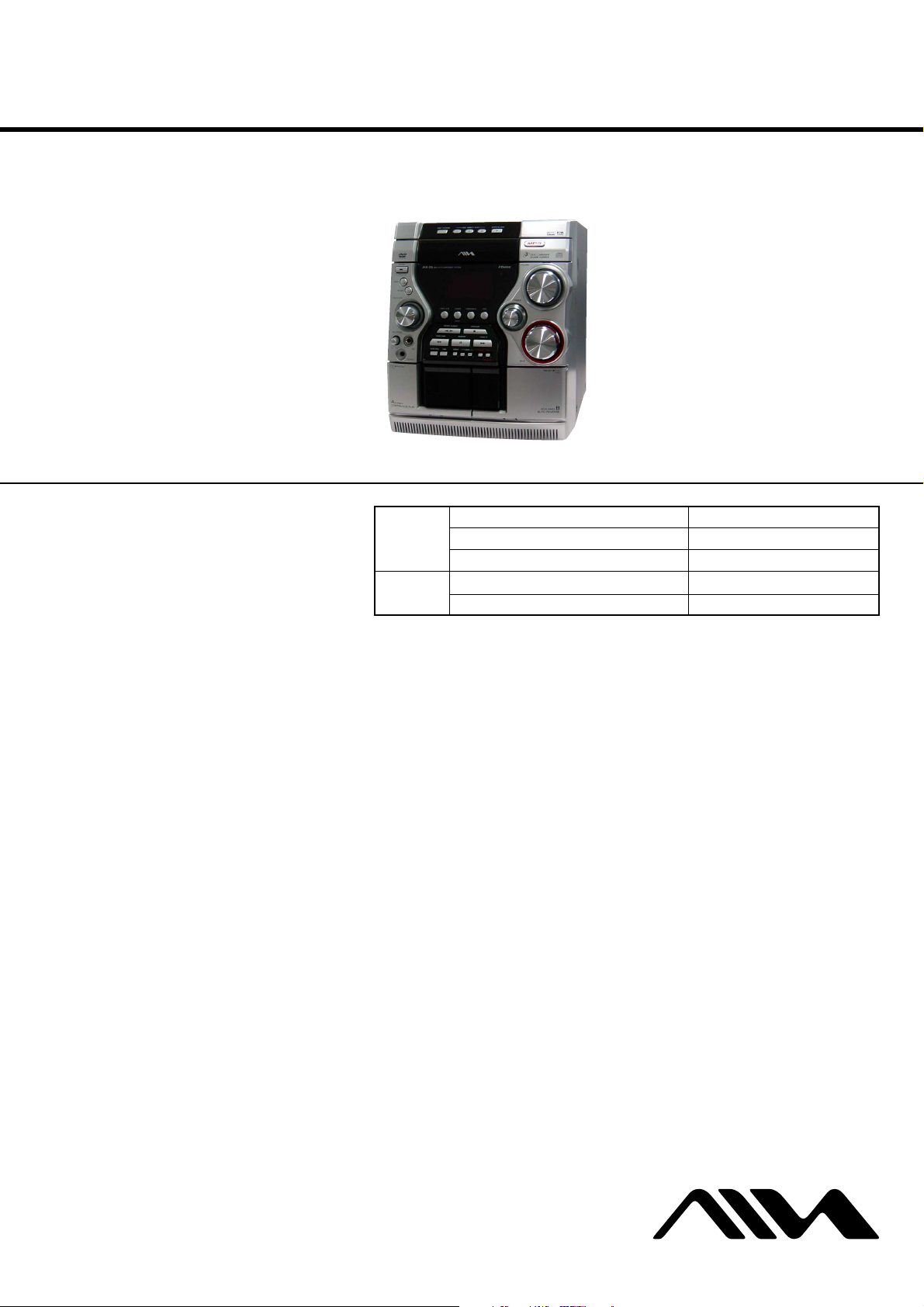
CX-JD5
SERVICE MANUAL
Ver. 1.2 2005.05
• CX-JD5 is the amplifier, DVD player, tape
deck and tuner section in JAX-D5.
This system incorporates Dolby* Digital, Dolby Pro
Logic (II) adaptive matrix surround decoder, and the
DTS** Digital Surround System.
*Manufactured under license from Dolby
Laboratories.
“Dolby”, “Pro Logic” and the double-D symbol are
trademarks of Dolby Laboratories.
** Manufactured under license from Digital Theater
Systems, Inc. “DTS” and “DTS Digital Surround”
are registered trademarks of Digital Theater
Systems, Inc.
US and foreign patents licensed from Dolby
Laboratories.
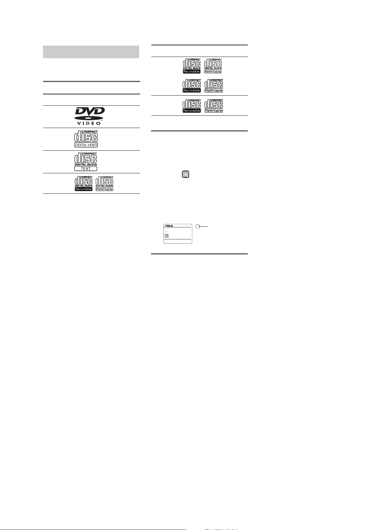
DVD
Section
Tape deck
Section
Model Name Using Similar Mechanism NEW
DVD Mechanism Type CDM74-DVBU23
Optical Traverse Unit Name DBU-1
Model Name Using Similar Mechanism NEW
Tape Transport Mechanism Type CWM43FR16/CWM43FR26
AEP Model
E Model
Australian Model
Amplifier section
The following measured at AC 120, 127, 220, 240 V,
50/60 Hz
Rated Power Output at Stereo mode
Continuous RMS power output (reference)
Front speaker: 90 + 90 watts
(6 ohms at 1 kHz, 10%
THD)
Center speaker: 30 watts (8 ohms at 1 kHz,
10% THD)
Surround speaker: 30 watts
(8 ohms at 1 kHz, 10%
THD)
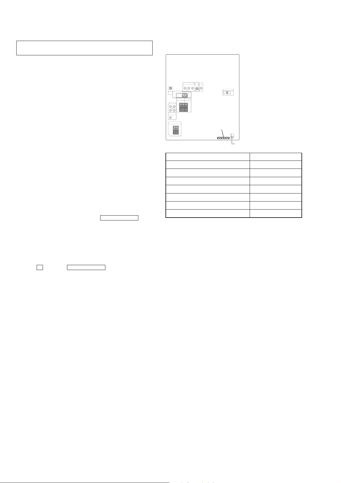
Inputs
MD/VIDEO (AUDIO) IN (phono jacks):
voltage 450/250 mV,
impedance 47 kilohms
MIC (phone jack): sensitivity 1 mV,
impedance 10 kilohms
Outputs
MD/VIDEO (AUDIO) OUT (phono jacks):
voltage 250 mV,
impedance 1 kilohm
SPECIFICATIONS
VIDEO OUT (phono jack):
S-VIDEO OUT (4-pin/mini-DIN jack):
COMPONENT VIDEO OUT:
PHONES (stereo mini jack):
Front speaker: Use only the supplied
Surround speaker: Use only the supplied
Center speaker: Use only the supplied
SUB WOOFER OUT: voltage 1 V,
max. output level
1 Vp-p, unbalanced, Sync
negative, load impedance
75 ohms
Y: 1 Vp-p, unbalanced,
Sync negative,
C: 0.286 Vp-p, load
impedance 75 ohms
Y: 1 Vp-p, 75 ohms
B
, PR: 0.7 Vp-p, 75 ohms
P
accepts headphones of
8ohms or more
speaker SX-JD5
speaker SX-JD5R
speaker SX-JD5C
impedance 1 kilohm
Disc player section
System Compact disc and digital
audio and video system
Laser Semiconductor laser
(DVD: λ=657 nm,
CD: λ=793 nm)
Emission duration:
continuous
Frequency response DVD (PCM 48 kHz):
2 Hz – 22 kHz (±1 dB)
CD: 2 Hz – 20 kHz (±1 dB)
Video color system format
NTSC, PAL
Tape deck section
Recording system 4-track 2-channel stereo
Frequency response 40 – 13,000 Hz (±3 dB),
using Sony TYPE I
cassette
– Continued on next page –
DVD DECK RECEIVER
9-961-039-03 Sony Corporation
2005E05-1 Personal Audio Group
© 2005.05 Published by Sony Engineering Corporation
Page 2
CX-JD5
Tuner section
FM stereo, FM/AM superheterodyne tuner
FM tuner section
Tuning range 87.5 – 108.0 MHz
Antenna FM lead antenna
Antenna terminals 75 ohm unbalanced
Intermediate frequency 10.7 MHz
AM tuner section
Tuning range
Latin American models: 530 – 1,710 kHz
Saudi Arabian model: 531– 1,602 kHz (with the
Other models: 531 – 1,602 kHz (with the
Antenna AM loop antenna
Antenna terminals External antenna terminal
Intermediate frequency 450 kHz
General
Power requirements
European model: 230 V AC, 50/60 Hz
Australian model: 230 – 240 V AC, 50/60 Hz
Saudi Arabian model: 120 – 127 V, 220 V or
Other models: 120 V, 220 V or 230 –
Power consumption
(with the interval set at
10 kHz)
531 – 1,710 kHz
(with the interval set at
9kHz)
interval set at 9 kHz)
interval set at 9 kHz)
530 – 1,710 kHz (with the
interval set at 10 kHz)
230 – 240V AC,
50/60 Hz
Adjustable with voltage
selector
240 V AC, 50/60 Hz
Adjustable with voltage
selector
255 watts
0.4 watts (in Power Saving
Mode, European Model
Only)
Notes on chip component replacement
•Never reuse a disconnected chip component.
• Notice that the minus side of a tantalum capacitor may be damaged by heat.
Flexible Circuit Board Repairing
•Keep the temperature of the soldering iron around 270 ˚C during repairing.
• Do not touch the soldering iron on the same conductor of the
circuit board (within 3 times).
• Be careful not to apply force on the conductor when soldering
or unsoldering.
CAUTION
Use of controls or adjustments or performance of procedures
other than those specified herein may result in hazardous radiation exposure.
The following caution label is located inside the unit.
This appliance is classified
CLASS 1 LASER PRODUCT
LUOKAN 1 LASER LAITE
KLASS 1 LASER APPARAT
as a CLASS 1 LASER
product.
This label is located on the
rear exterior.
The following caution label is located inside the apparatus.
Dimensions (w/h/d)
Mass
Design and specifications are subject to change
without notice.
Approx. 280 × 330 ×
405 mm
Approx. 11.75 kg
SAFETY-RELATED COMPONENT WARNING!!
COMPONENTS IDENTIFIED BY MARK 0 OR DOTTED
LINE WITH MARK 0 ON THE SCHEMATIC DIAGRAMS
AND IN THE PARTS LIST ARE CRITICAL TO SAFE
OPERATION. REPLACE THESE COMPONENTS WITH
SONY PARTS WHOSE PART NUMBERS APPEAR AS
SHOWN IN THIS MANUAL OR IN SUPPLEMENTS PUBLISHED BY SONY.
UNLEADED SOLDER
Boards requiring use of unleaded solder are printed with the leadfree mark (LF) indicating the solder contains no lead.
(Caution: Some printed circuit boards may not come printed with
the lead free mark due to their particular size)
: LEAD FREE MARK
Unleaded solder has the following characteristics.
• Unleaded solder melts at a temperature about 40 ˚C higher than
ordinary solder.
Ordinary soldering irons can be used but the iron tip has to be
applied to the solder joint for a slightly longer time.
Soldering irons using a temperature regulator should be set to
about 350 ˚C.
Caution: The printed pattern (copper foil) may peel away if the
heated tip is applied for too long, so be careful!
• Strong viscosity
Unleaded solder is more viscou-s (sticky, less prone to flow)
than ordinary solder so use caution not to let solder bridges occur such as on IC pins, etc.
• Usable with ordinary solder
It is best to use only unleaded solder but unleaded solder may
also be added to ordinary solder.
2
Page 3
CX-JD5
• DVD-RWs in VR mode (DVD-RWs created
in VR (Video Recording) mode allow the
contents to be programed or edited.)
• DVD-ROMs
• DVD Audio discs
•A DVD with a different region code.
•Audio tracks in MP3PRO format.
•A disc that has a non-standard shape (e.g.,
card, heart).
•A disc with paper or stickers on it.
•A disc that has the adhesive, cellophane tape,
or a sticker still left on it.
*1
ISO9660 Format
The most common international standard for the
logical format of files and folders on a CD-ROM.
There are severa l specification levels. In Leve l 1, file
names must be in the 8.3 format (no more than eight
characters in the name, no more than three characters
in the extension “.MP3” or “.JPG”) and in capital
letters. Folder names can be no longer than eight
characters. There can be no more than eight nested
folder levels. Level 2 sp ecifications allow file names
and folder names up to 31 characters long. Each
folder can have up to 8 trees.
For Joliet in the expansion format (file and folder
names can have up to 64 characters) m ake sure of the
contents of the writing software, etc.
*2
Multi Session
This is a recording method that enables adding of
data using the Track -At-Once method. Conventional
CDs begin at a CD control area called the Lead-in
and end at an area called Lead-out. A Multi Session
CD is a CD having multiple sessions, with each
segment from Lead-in to Lead-out regarded as a
single session.
CD-Extra: This format records audio (audio CD
data) on the tracks in se ssion 1 and data on the tracks
in session 2.
Playable discs
You can play back the following discs on this
system. Other discs cannot be played back.
List of playable discs
Format of
discs
DVD VIDEOs Audio +
VIDEO CDs Audio +
Audio CDs Audio
CD-R/CD-RW
(audio data)
Disc logo Contents
Video
Video
Audio
Format of
discs
CD-R/CD-RW
(MP3 files)
CD-R/CD-RW
(JPEG files)
The “DVD VIDEO” logo is a trademark.
Disc logo Contents
Audio
Video
Region code of DVDs you can
play on this system
Your system has a region code printed on the
back of the unit and will only play DVDs labeled
with identical region code.
DVDs labeled will also be played on this
ALL
system.
If you try to play any other DVD, the message
“Playback prohibited by area limitations.” will
appear on the TV screen. Depending on the
DVD, no region code indication may be labeled
even though playing the DVD is prohibited by
area restrictions.
MODEL NO.
CX-JD5
X
DVD DECK RECEIVER
AC: 120V/220V/230-240V
50/60Hz XXXW
SERIAL NO.
Sony Corporation
Region code
Discs that this system cannot
play
•CD-ROMs (except for extension “.MP3,”
“.JPG,” or “.JPEG”)
•CD-Rs/CD-RWs other than those recorded in
the following formats:
–music CD format
–video CD format
–MP3/JPEG format that conforms to
ISO9660*
Session*
•Data part of CD-Extras
•Super Audio CDs
•Progressive JPEG format files cannot be
played on this system.
1
Level 1/Level 2, Joliet or Multi
2
3
Page 4

CX-JD5
Notes on discs
•This system can play CD-R/CD-RW discs
edited by the user. However, note that
playback of some discs may not be possible
depending on the recording device used for
recording or the disc condition.
•Discs recorded on CD-R/CD-RW drives may
not be played back because of scratches, dirt,
recording condition or the driver’s
characteristics.
•CD-R and CD-RW discs that have not been
correctly finalized (processing to allow play
by a normal CD player) cannot be played.
•CD-R and CD-RW discs recorded in multisession that have not ended by “closing the
session” are not supported.
•The system may be unable to play MP3/JPEG
format files that do not have the extender
“.MP3”, “.JPG”, or “.JPEG”.
•Attempting to play non-MP3/JPEG format
files that have the extender “.MP3”, “.JPG”,
or “.JPEG” may result in noise or
malfunction. Playback is possible up to 8
levels.
•With formats other than ISO9660 level 1 and
2, folder names or file names may not be
displayed correctly.
•The following discs take a longer time to start
playback.
–a disc recorded with complicated tree
structure.
–a disc recorded in Multi Session.
–a disc to which data can be added (non-
finalized disc).
•Some CD-Rs, CD-RWs, DVD-Rs or DVDRWs (in video mode) (DVD-RWs created in
video mode have the same format as a DVD
VIDEO) cannot be played on this system
depending upon the recording quality or
physical condition of the disc, or the
characteristics of the recording device.
Furthermore, the disc will not play if it has not
been correctly finalized. For more
information, see the operating instructions for
the recording device.
•A disc recorded in packet write format cannot
be played.
Note on playback operations
of DVDs and VIDEO CDs
Some playback operations of DVDs and VIDEO
CDs may be intentionally set by software
producers. Since this system plays DVDs and
VIDEO CDs according to the disc contents the
software producers designed, some playback
features may not be available. Also, refer to the
instructions supplied with the DVDs or VIDEO
CDs.
Copyrights
This product incorporates copyright protection
technology that is protected by U.S. patents and
other intellectual property rights. Use of this
copyright protection technology must be
authorized by Macrovision, and is intended for
home and other limited viewing uses only unless
otherwise authorized by Macrovision. Reverse
engineering or disassembly is prohibited.
Music discs encoded w ith
copyright prote ction
technologies
This product is designed to playback discs that
conform to the Compact Disc (CD) standard.
Recently, various music discs encoded with
copyright protection technologies are marketed
by some record companies. Please be aware that
among those discs, there are some that do not
conform to the CD standard and may not be
playable by this product.
Cautions w hen pla ying a disc
that is recorded in Multi
Session
•This system can play Multi Session CDs when
an MP3 audio track is contained in the first
session. Any subsequent MP3 audio tracks
recorded in later sessions can also be played
back.
•This system can play Multi Session CDs when
a JPEG image file is contained in the first
session. Any subsequent JPEG image files
recorded in later sessions can also be played
back.
•If audio tracks and images in music CD
format or video CD format are recorded in the
first session, only the first session will be
played back.
4
Page 5

TABLE OF CONTENTS
CX-JD5
1. SERVICING NOTES ................................................ 6
2. GENERAL
Location of Controls ....................................................... 8
3. DISASSEMBLY
3-1. Disassembly Flow ........................................................... 9
3-2. Steel Cabinet Case .......................................................... 10
3-3. Tray Panel........................................................................ 10
3-4. DVD Mechanism Deck (CDM74-DVBU23) ................. 11
3-5. Front Panel Section ......................................................... 11
3-6. Mechanism Deck (CWM43FR16/CWM43FR26) ......... 12
3-7. Back Panel Section.......................................................... 12
3-8. MAIN Board Section ...................................................... 13
3-9. MAIN Board ................................................................... 13
3-10. I-BASS Board ................................................................. 14
3-11. FRONT AMP Board, SURROUND AMP Board........... 14
3-12. TRANS Board ................................................................. 15
3-13. MB03 Board .................................................................... 15
3-14. VIDEO Board.................................................................. 16
3-15. DRIVER Board, SW Board ............................................ 16
3-16. Table Assy ....................................................................... 17
3-17. MOTOR (TB) Board ....................................................... 17
3-18. MOTOR (LD) Board....................................................... 18
3-19. RF Board ......................................................................... 18
3-20. Optical Traverse Unit (DBU-1) ...................................... 19
4. TEST MODE.............................................................. 20
5. ELECTRICAL ADJUSTMENTS......................... 30
6. DIAGRAMS
6-1. Block Diagram – DVD DSP (1/2) Section –................. 31
6-2. Block Diagram – DVD DSP (2/2) Section –................. 32
6-3. Block Diagram – TUNER/TAPE DECK Section – ...... 33
6-4. Block Diagram – MAIN Section – ................................ 34
6-5. Block Diagram – AMP Section – .................................. 35
6-6. Block Diagram
– DISPLAY/POWER SUPPLY Section – ...................... 36
6-7. Note for Printed Wiring Boards
and Schematic Diagrams ................................................ 37
6-8. Printed Wiring Board – RF Section –............................ 38
6-9. Schematic Diagram – RF Section –............................... 39
6-10. Printed Wiring Boards – CHANGER Section – ............ 40
6-11. Schematic Diagram – CHANGER Section – ................ 41
6-12. Printed Wiring Board
– MB Section (Component Side) – ................................ 42
6-13. Printed Wiring Board
– MB Section (Conductor Side) – .................................. 43
6-14. Schematic Diagram – MB Section (1/8) – .................... 44
6-15. Schematic Diagram – MB Section (2/8) – .................... 45
6-16. Schematic Diagram – MB Section (3/8) – .................... 46
6-17. Schematic Diagram – MB Section (4/8) – .................... 47
6-18. Schematic Diagram – MB Section (5/8) – .................... 48
6-19. Schematic Diagram – MB Section (6/8) – .................... 49
6-20. Schematic Diagram – MB Section (7/8) – .................... 50
6-21. Schematic Diagram – MB Section (8/8) – .................... 51
6-22. Printed Wiring Board – MAIN Section – ...................... 53
6-23. Schematic Diagram – MAIN Section (1/4) – ................ 54
6-24. Schematic Diagram – MAIN Section (2/4) – ................ 55
6-25. Schematic Diagram – MAIN Section (3/4) – ................ 56
6-26. Schematic Diagram – MAIN Section (4/4) – ................ 57
6-27. Printed Wiring Board – I-BASS Section – .................... 58
6-28. Schematic Diagram – I-BASS Section – ....................... 59
6-29. Printed Wiring Board – FRONT AMP Section – .......... 60
6-30. Schematic Diagram – FRONT AMP Section –............. 61
6-31. Printed Wiring Board
– SURROUND AMP Section – ...................................... 62
6-32. Schematic Diagram – SURROUND AMP Section –.... 63
6-33. Printed Wiring Boards – PANEL Section – .................. 64
6-34. Schematic Diagram – PANEL Section –....................... 65
6-35. Printed Wiring Boards – KEY Section – ....................... 66
6-36. Schematic Diagram – KEY Section – ........................... 67
6-37. Printed Wiring Board – VIDEO Section – .................... 68
6-38. Schematic Diagram – VIDEO Section – ....................... 69
6-39. Printed Wiring Board – TRANS Section – ................... 70
6-40. Schematic Diagram – TRANS Section – ...................... 71
6-41. Printed Wiring Board – SUB TRANS Section –........... 72
6-42. Schematic Diagram – SUB TRANS Section – ............. 73
6-43. IC Pin Function Description ........................................... 78
7. EXPLODED VIEWS
7-1. Case Section .................................................................... 92
7-2. Front Panel Section-1...................................................... 93
7-3. Front Panel Section-2...................................................... 94
7-4. Front Panel Section-3...................................................... 95
7-5. Front Panel Section-4...................................................... 96
7-6. Chassis Section-1 ............................................................ 97
7-7. Chassis Section-2 ............................................................ 98
7-8. DVD Mechanism Deck Section-1
(CDM74-DVBU23) ........................................................ 99
7-9. DVD Mechanism Deck Section-2
(CDM74-DVBU23) ....................................................... 100
7-10. DVD Mechanism Deck Section-3
(CDM74-DVBU23) ....................................................... 101
7-11. DVD Mechanism Deck Section-4
(CDM74-DVBU23) ....................................................... 102
8. ELECTRICAL PARTS LIST .............................. 103
5
Page 6
CX-JD5
Ver 1.1
SECTION 1
SER VICING NOTES
NOTES ON HANDLING THE OPTICAL PICK-UP
BLOCK OR BASE UNIT
The laser diode in the optical pick-up block may suffer electrostatic break-down because of the potential difference generated
by the charged electrostatic load, etc. on clothing and the human
body.
During repair, pay attention to electrostatic break-down and also
use the procedure in the printed matter which is included in the
repair parts.
The flexible board is easily damaged and should be handled with
care.
NOTES ON LASER DIODE EMISSION CHECK
The laser beam on this model is concentrated so as to be focused
on the disc reflective surface by the objective lens in the optical
pick-up block. Therefore, when checking the laser diode emission, observe from more than 30 cm away from the objectiv e lens.
LASER DIODE AND FOCUS SEARCH OPERATION
CHECK
Carry out the “S curve check” in “CD section adjustment” and
check that the S curve waveforms is output three times.
DVD TRAY LOCK MODE
•This mode let you lock the disc trays. When this mode is activated, the disc tray will not open when
or [DISC CHANGE] button is pressed. The message “LOCKED”
will be displayed in the will be displayed on the fluorescent
indicator tube.
Z OPEN/CLOSE button
• MODEL IDENTIFICATION
– Rear Cover –
PART No.
MODEL PART No.
Singapore and Malaysia models 4-247-797-0
E model 4-247-797-1
Thai model 4-247-797-5
AEP and CIS models 4-247-797-7
Chilean and Peruvian models 4-247-797-8
Australian model 4-247-797-9
Saudi Arabia model 4-247-798-4
[]
[]
[]
[]
[]
[]
[]
Procedure:
1. Press [POWER] button to turn the set ON.
2. Select DVD function.
3. Press x button and Z OPEN/CLOSE button simultaneously
and hold down until “LOCKED” or “UNLOCKED” displayed
on the fluorescent indicator tube (around 5 seconds).
6
Page 7
HOW TO OPEN THE DISC TRAY WHEN POWER SWITCH TURNS OFF.
1 Remove the steel cabinet case.
2 Turn the loading gear
in the direction of arrow A.
A
3 Pull-out the disc tray.
CX-JD5
7
Page 8
CX-JD5
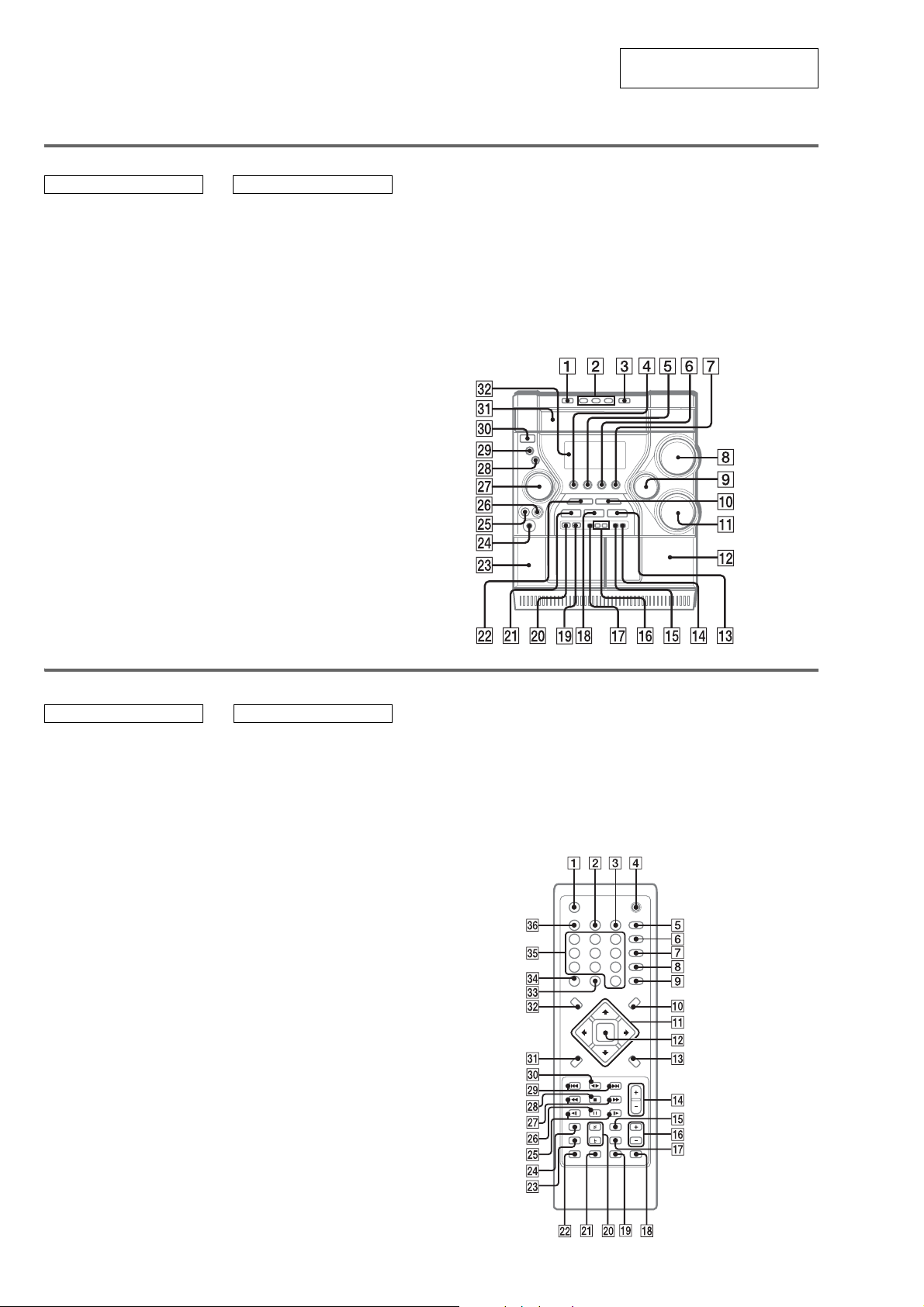
• LOCATION OF CONTROLS
Main unit
ALPHABETICAL ORDER
ALBUM +/– qh
BASS qa
CD SYNC qg
Deck A wd
Deck B qs
DIR (TAPE B) bB ws
DISC DIRECT PLAY 1/2/3 2
DISC SKIP/EX-CHANGE 1
Disc tray ea
DISPLAY qj
Display window es
DVD 7
ENTER wk
i-Bass ql
MD (VIDEO) 6
MIC jack wh
MIC LEVEL wg
MODE wl
MULTI JOG wj
OPEN/CLOSE Z 3
PHONES jack wf
REC PAUSE/START qf
SOUND FIELD w;
TAPE A/B 4
TREBLE/MIDDLE 9
TUNER/BAND 5
TUNING – ./m wa
TUNING + M/> qd
VOLUME control 8
BUTTON DESCRIPTIONS
[/1 (power) e;
X (pause) qk
Z (OPEN/CLOSE) 3
x (stop) q;
M/> (fast forward/
TUNING +) qd
nN DIRECTION ws
./m (rewind/TUNING –)
wa
SECTION 2
GENERAL
This section is extracted from
instruction manual.
Remote control
ALPHABETICAL ORDER BUTTON DESCRIPTIONS
ALBUM +/– qh
AMP MENU qg
CLEAR 9
CLOCK/TIMER SELECT 3
CLOCK/TIMER SET 2
DISPLAY 1
D.SKIP qk
DVD DISPLAY qd
DVD MENU q;
DVD SETUP qj
DVD TOP MENU es
ECHO wd
ENTER qs
FM MODE ql
FUNCTION*
KARAOKE wf
KEY CONTROL
i-Bass 6
Number buttons eg
PLAY MODE 7
PRESET –/PREV . wl
PRESET +/NEXT > wl
REPEAT 8
O RETURN ea
SELECT nN e;
SLOW –/+ wg
SHIFT*
SLEEP eh
SOUND FIELD 5
TUNER/BAND ed
TUNER MEMORY wa
TUNING –/+ wj
VOL +/– qf
1
ef
#/2 w;
2
ws
[/1 4
x (stop) wk
nN (SELECT) e;
X (pause) wh
M/m/</, qa
m (TUNING –) wj
M (TUNING +) wj
. (PRESET –/PREV) wl
> (PRESET +/NEXT) wl
t (SLOW –) wg
T (SLOW +) wg
# (KEY CONTROL) w;
2 (KEY CONTROL) w;
*1
Switches the active function among
CD, TAPE, TUNER, MD (VIDEO)
and DVD.
*2
Press and hold SHIFT and press m ,
, or < to do the following;
SHIFT + m = SUBTITLE
SHIFT + , = ANGLE
SHIFT + < = AUDIO
e.g.)Press and hold SHIFT, and
press m to active the subtitle menu.
8
Page 9
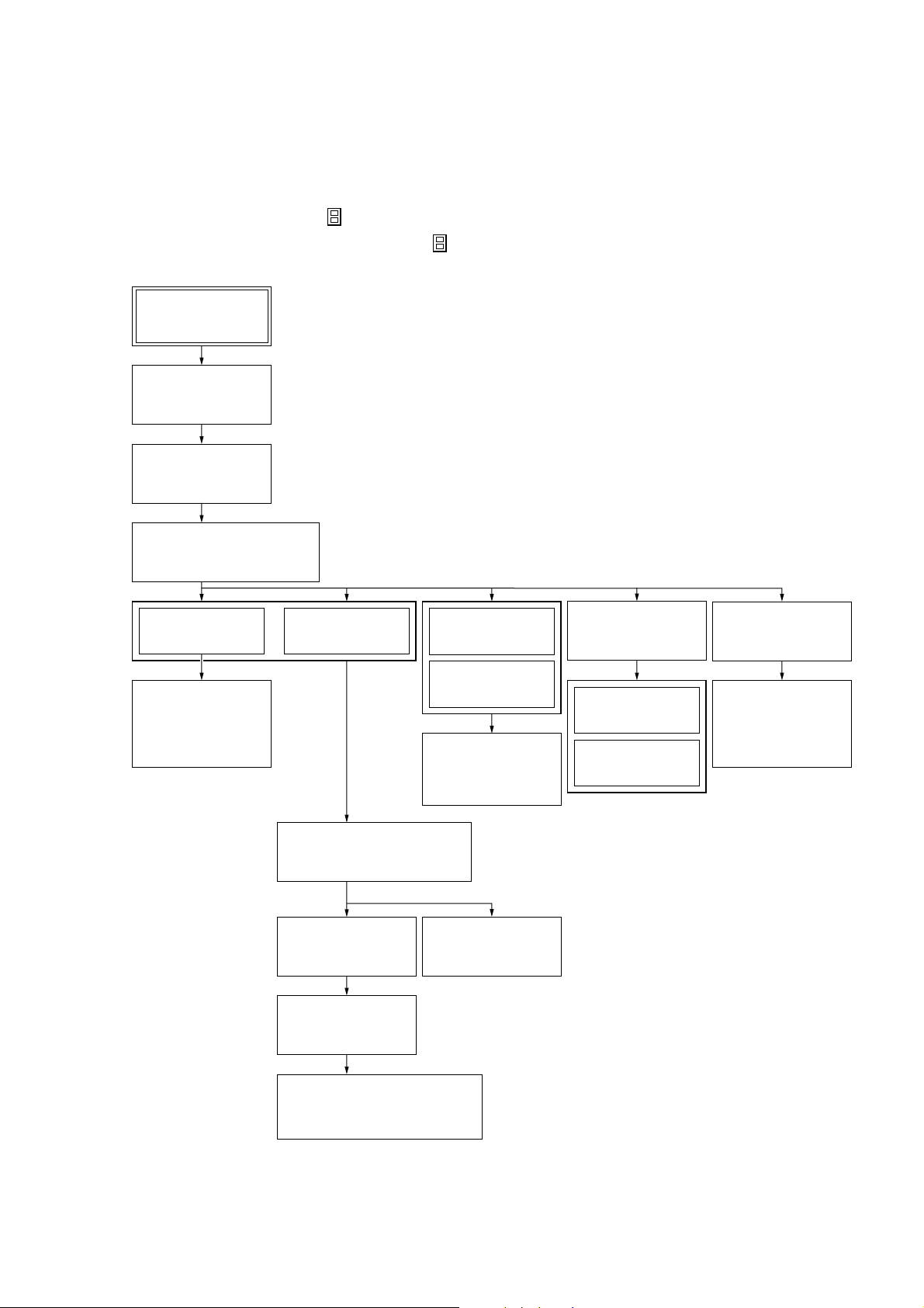
SECTION 3
DISASSEMBLY
• This set can be disassembled in the order shown below.
3-1. DISASSEMBLY FLOW
Note 1: The process described in can be performed in any order.
Note 2: Without completing the process described in , the next process can not be performed.
Set
3-2. STEEL
CABINET CASE
(Page 10)
3-3. TRAY PANEL
(Page 10)
CX-JD5
3-4. DVD MECHANISM DECK
(CDM74-DVBU23)
(Page 11)
3-5. FRONT PANEL
SECTION
(Page 11)
3-6. MECHANICAL
DECK
(CWM43FR16/
CWM43FR26)
(Page 12)
3-7. BACK PANEL
3-8. MAIN BOARD SECTION
3-9. MAIN BOARD
SECTION
(Page 12)
(Page 13)
(Page 13)
3-13. MB03
BOARD
(Page 15)
3-14. VIDEO
BOARD
(Page 16)
3-15. DRIVER
BOARD,
SW BOARD
(Page 16)
3-12. TRANS
BOARD
(Page 15)
3-16. TABLE ASSY
(Page 17)
3-17. MOTOR (TB)
BOARD
(Page 17)
3-18. MOTOR (LD)
BOARD
(Page 18)
3-19. RF BOARD
(Page 18)
3-20. OPTICAL
TRAVERSE
UNIT
(DBU-1)
(Page 19)
3-10. I-BASS BOARD
(Page 14)
3-11. FRONT AMP BOARD,
SURROUND AMP BOARD
(Page 14)
9
Page 10
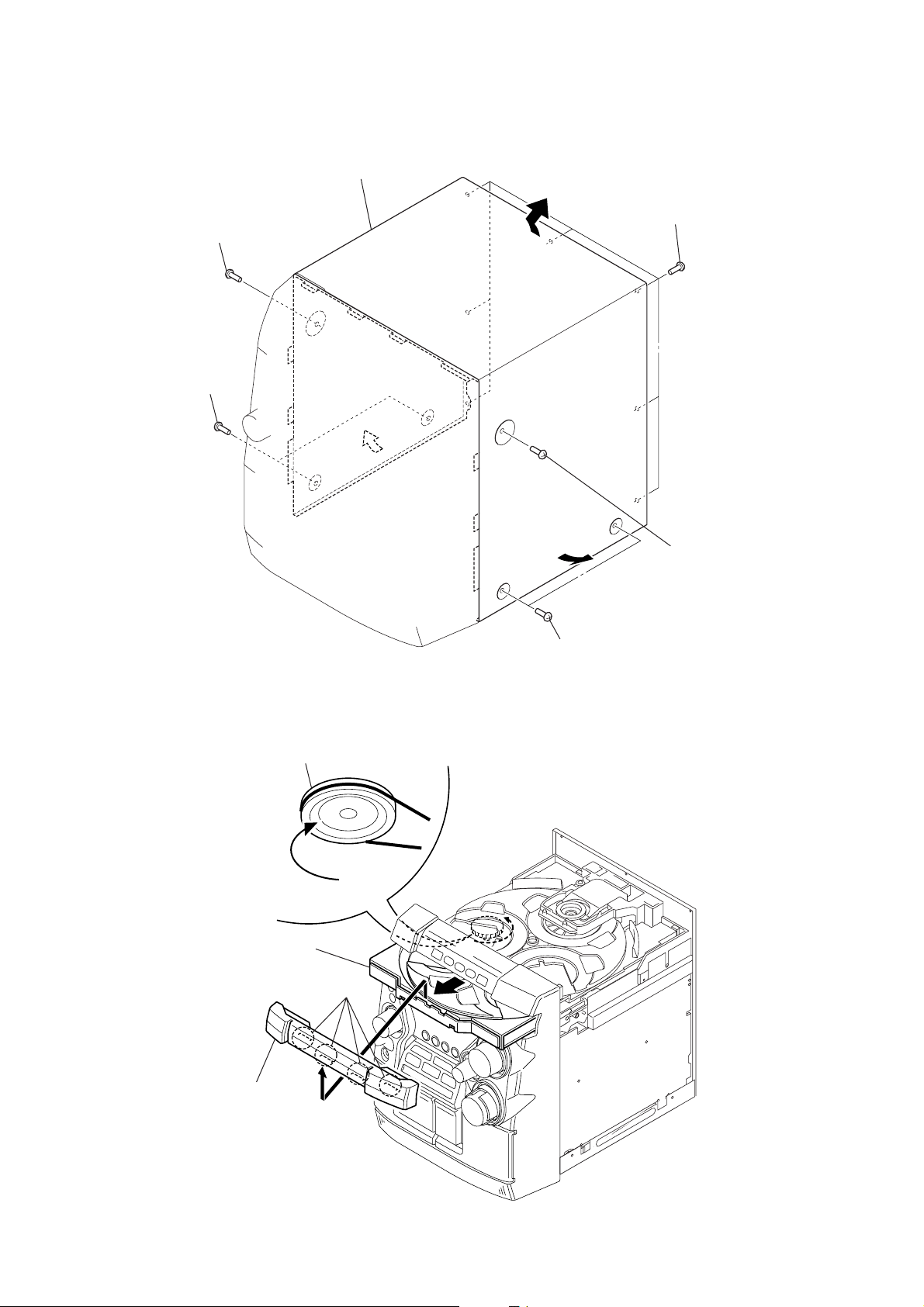
CX-JD5
)
Note: Follow the disassembly procedure in the numerical order given.
3-2. STEEL CABINET CASE
4
steel cabinet case
3
screw
(case3 TP2)
3
two screws
(case3 TP2)
1
seven screws
(BVTT3
×
6)
3-3. TRAY PANEL
1
2
Turn the loading gear
in the direction of arrow A.
A
Pull-out the disc table.
3
four claws
2
two screws
(case3 TP2)
2
screw
(case3 TP2
10
4
tray panel
Page 11
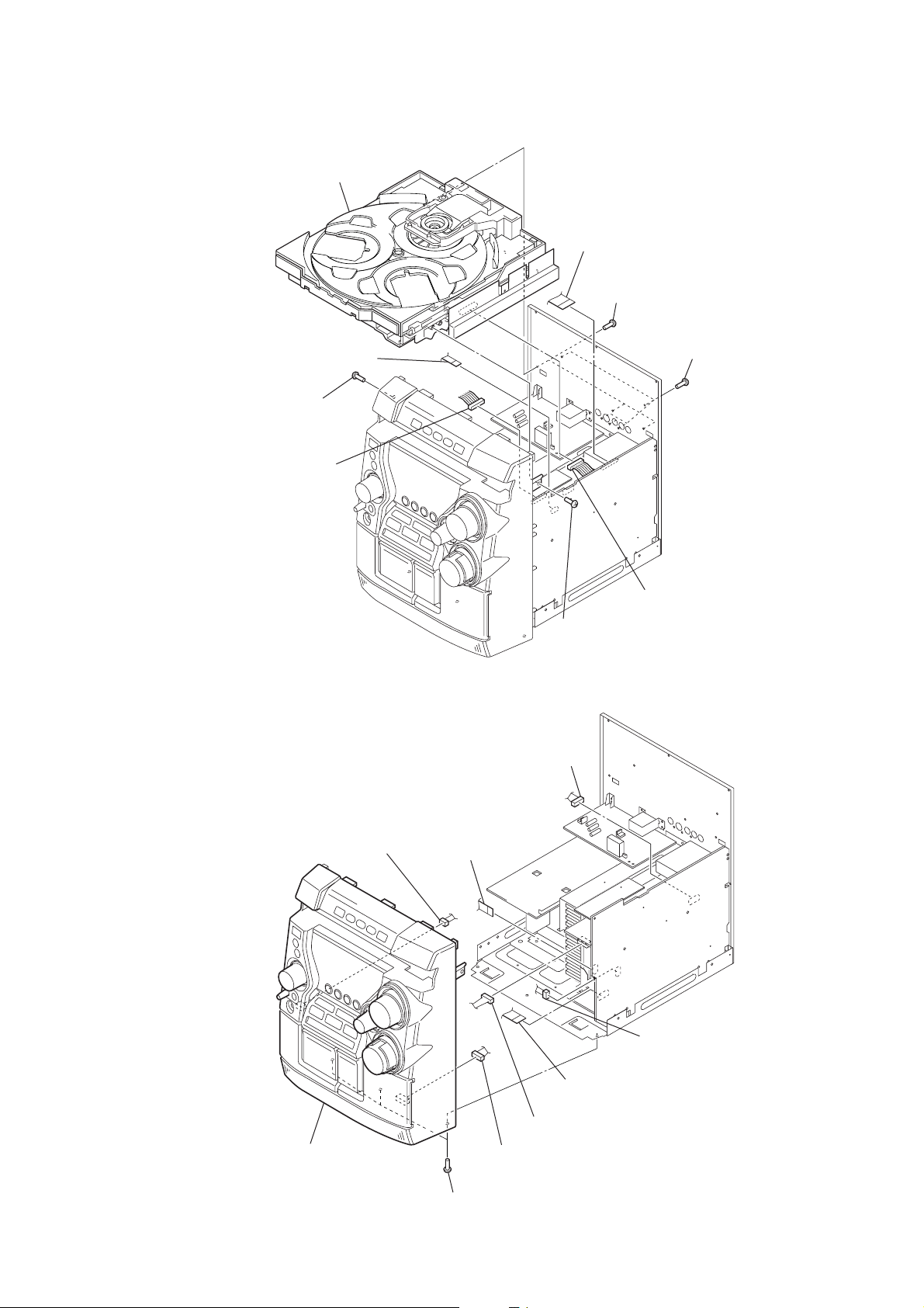
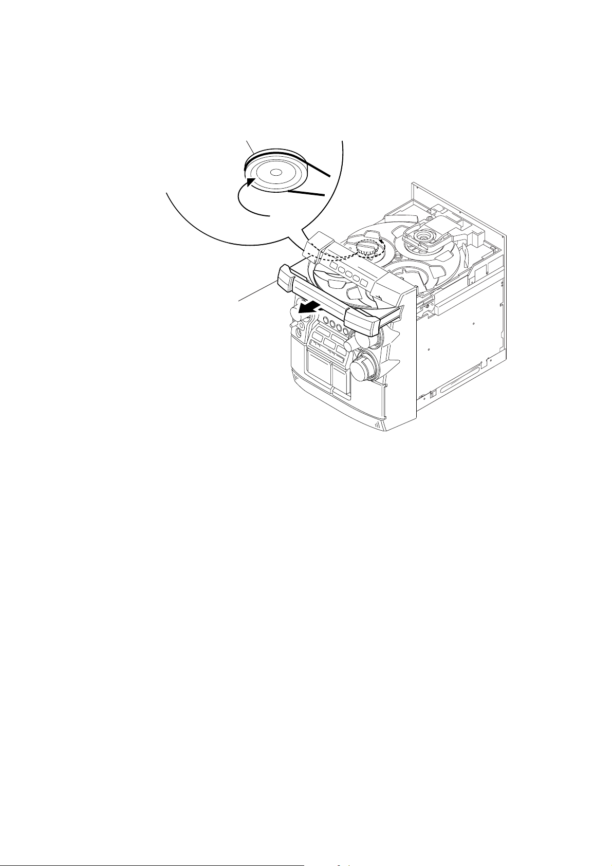
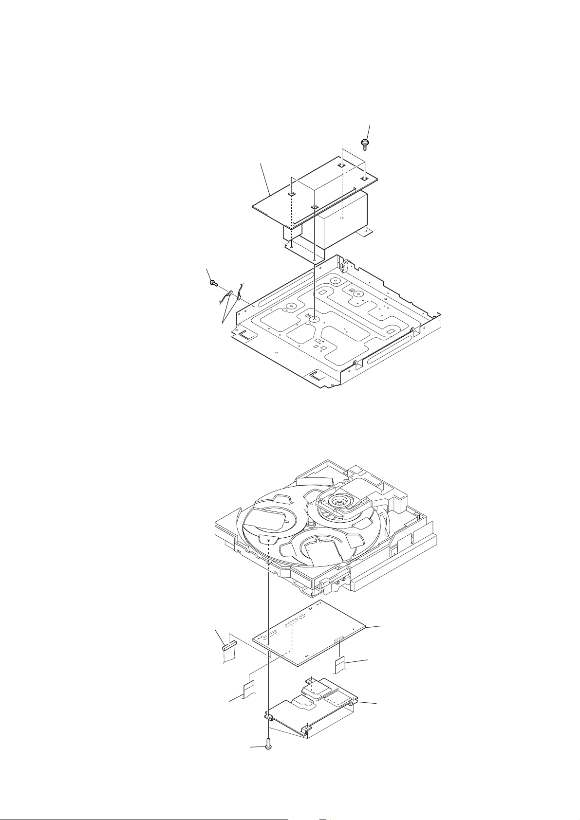
3-4. DVD MECHANISM DECK (CDM74-DVBU23)
)
)
5
DVD mechanism deck
(CDM74-DVBU23)
7
wire (flat type) (6 core)
(CN101)
2
screw
(BVTP3 × 10)
6
connector (CN543)
9
wire (flat type) (25 core)
(CN301)
4
three screws
(BVTT3 × 6)
3
five screws
(BVTP3 × 8
CX-JD5
3-5. FRONT PANEL SECTION
1
connector (CN503)
4
connector (CN902)
2
wire (flat type) (9 core)
(CN706)
1
screw
(BVTP3 × 10)
8
connector (CN804)
6
connector (CN802
8
front panel section
7
three screws
(BVTP3 × 10)
3
wire (flat type) (12 core)
(CN805)
5
connector (CN304)
9
connector (mechanical deck)
11
Page 12
CX-JD5
)
)
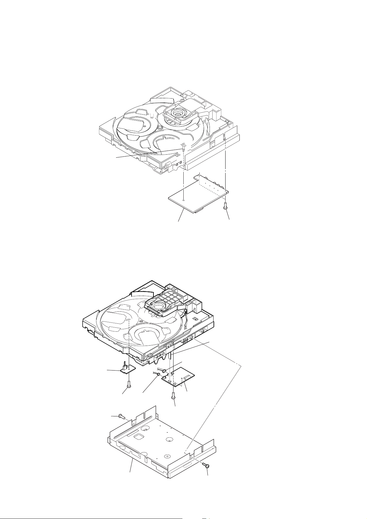
3-6. MECHANICAL DECK (CWM43FR16/CWM43FR26)
3
mechanical deck
(CWM43FR16/CWM43FR26)
4
1
wire (flat type) (13 core)
ground mechanical plate
2
six screws
(BVTP3
×
10
3-7. BACK PANEL SECTION
4
wire (flat type)
(11 core) (except AEP)
(15 core) (AEP)
(CN102)
8
three screws
(BVTT3
1
2
connector
(CN902)
×
3
connector
(CN901)
6)
connector
(CN903)
9
back panel section
0
connector
(CN704)
5
two screws
(BVTT3
7
×
6
five screws
(BVTP3
screw
(BVTT3
6)
×
8
×
6)
12
Page 13
3-8. MAIN BOARD SECTION
d
1
connector
(CN914)
4
two screws
(BVTT3
3
two screws
(BVTT3
×
6)
CX-JD5
7
main board section
×
6)
6
two screws
(BVTP3
×
5
8)
screw
(BVTT3
×
6)
2
connector
(CN915)
3-9. MAIN BOARD
1
connector
(CN303)
3
connector
(CN901)
4
connector
(CN104)
7
main boar
5
two PC board holders
2
connector
(CN103)
6
two connectors
(CN705, CN707)
13
Page 14
CX-JD5
)
)
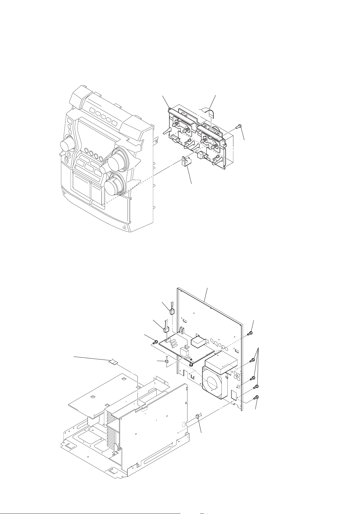
3-10. I-BASS BOARD
2
I-bass board
1
two screws
(BVTP3 × 8
3-11. FRONT AMP BOARD, SURROUND AMP BOARD
5
6
front amp board
surround amp board
2
3
two screws
(BVTP3
×
1
connector (CN305)
4
two screws
(BVTP3
connector (CN302)
10)
×
16
14
Page 15
3-12. TRANS BOARD
1
screw
(BVTT3 × 6)
4
trans board
3
four screws
(ITC+4-8R)
CX-JD5
3-13. MB03 BOARD
2
two earth lugs
3
connector
(CN102)
2
wire (flat type)
(17 core)(CN105)
4
four screws
(BVTT3 × 6)
6
MB03 board
1
wire (flat type) (29 core)
(CN501)
5
heat sink
15
Page 16
CX-JD5
)
)
3-14. VIDEO BOARD
2
PWB holder
3-15. DRIVER BOARD, SW BOARD
0
SW board
9
screw
(BVTP2.6)
2
screw
(BVTP3
×
8)
4
connector
(CN704)
3
video board
5
7
6
two screws
(BVTP2.6)
connector
(CN704)
driver board
1
two screws
(BVTT3 × 6
8
wire (flat type) (5 core
(CN702)
16
3
bracket (DVD)
1
screw
(BVTP3
×
8)
Page 17

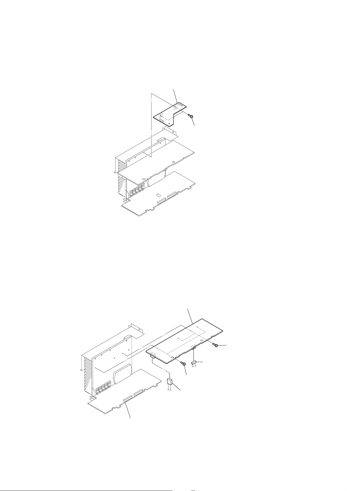
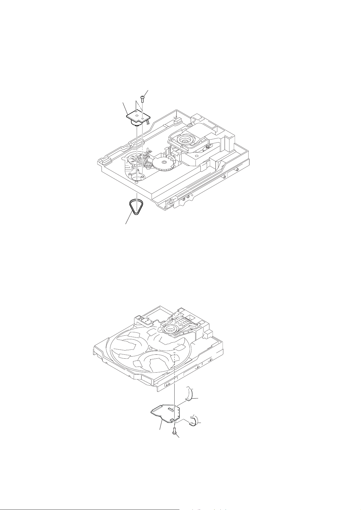
3-16. TABLE ASSY
)
6
table assy
5
two claws
CX-JD5
Ver. 1.2
3-17. MOTOR (TB) BOARD
2
Pull-out the table assy.
1
screw
(PTPWH M2.6)
2
tray
A
1
Turn the loading gear
in the direction of arrow A.
3
belt (table)
4
hook
3
wire (flat type) (5 core
(CN702)
4
connector
(CN731)
6
5
two screws
(BTTP M2.6)
motor (TB) board
17
Page 18
CX-JD5
)
3-18. MOTOR (LD) BOARD
3
motor (LD) board
2
two screws
(BTTP M2.6)
3-19. RF BOARD
1
belt (loading)
3
flexible flat cable
(24 core) (CN001
18
2
RF board
1
two screws
(BTTP 2.6)
4
flexible board
(CN003)
Page 19
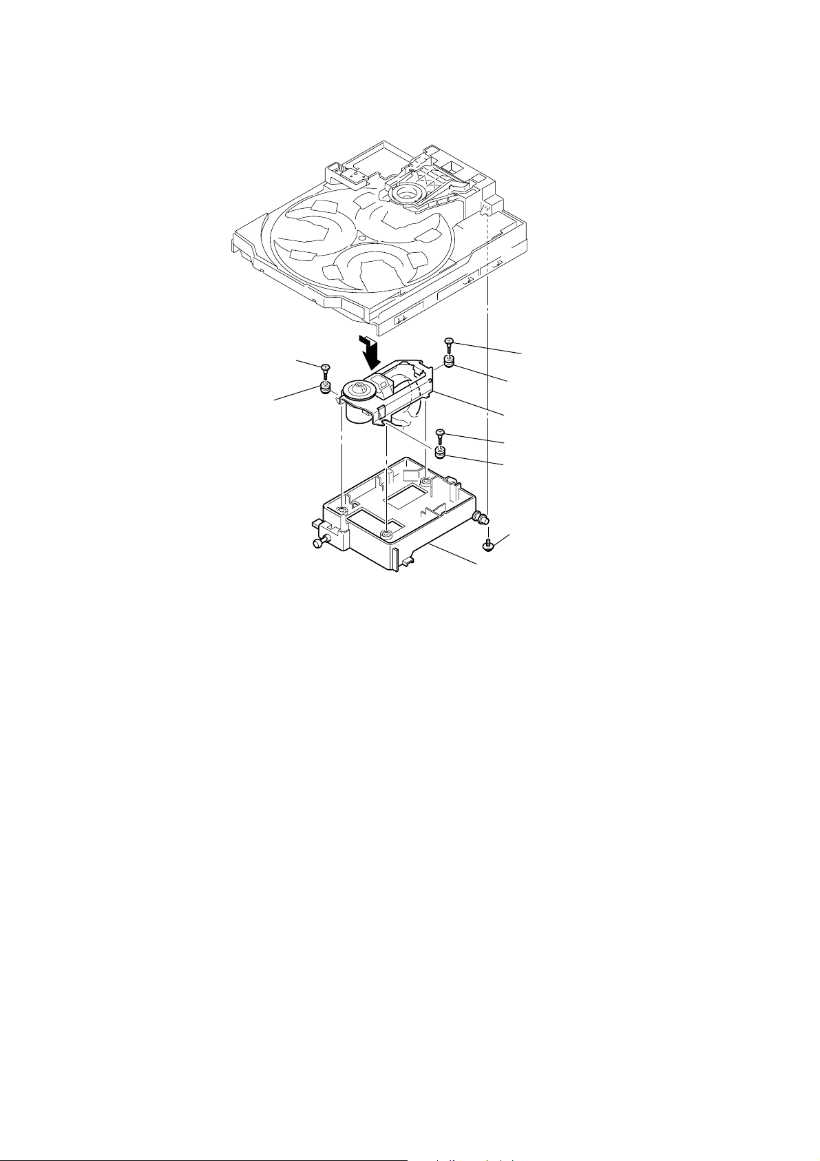
3-20. OPTICAL TRAVERSE UNIT (DBU-1)
CX-JD5
3
step
6
insulator
(HRC)
screw (M)
2
4
step
screw (M)
7
insulator
9
optical traverse unit (DBU-1)
5
step
screw (M)
8
insulator (HRC)
1
floating
0
holder (DBU) assy
screw (PTPWH M2.6)
19
Page 20

CX-JD5
SECTION 4
TEST MODE
[MC TEST MODE]
• This mode is used to check operations of the respective sections
of Amplifier, Tuner , and Tape.
Procedure:
* To enter MC Test Mode
1. P ress x button, [ENTER] but t on and [DISC 3] button
simultaneously, the message “TEST MODE” will be displayed
on the fluorescent indicator tube.
* Check of Amplifier
1. When [BASS] knob is turned clockwise, GEQ increases to its
maximum and a message “GEQ MAX” appears on the
fluorescent indicator tube.
2. When [BASS] knob is turned counter clockwise, GEQ
decreases to its minimum and a message “GEQ MIN” appears
on the fluorescent indicator tube.
3. When [SOUND FIELD] button is pressed, GEQ is set to flat
and a message “GEQ FLAT” appears on the fluorescent
indicator tube.
4. When the [VOLUME] knob is turned clockwise even slightly,
the sound volume increases to its maximum and a message
“VOL MAX” appears for two seconds, then the display returns
to the original display.
5. When the [VOLUME] knob is turned counter-clockwise even
slightly, the sound volume decreases to its minimum and a
message “VOL 0” appears for two seconds, then the display
returns to the original display.
* VACS ON/OFF Change Over
1. Press [i-Bass] button. The message “VACS OFF” or “VACS
ON” appears.
* Tape function
1. When a tape is inserted in Deck B and recording is started, the
function is changed to VIDEO automatically.
2. After recording is stopped by pressing
button will change the function to TAPE B and rewind Tape B
until the recording start position and playback of Tape B is
started. If the [REC PAUSE/ START] button is pressed for a
pause and pressed again to resume recording during recording
time, when tape deck B is rewind, tape deck B will be rewind
until the position where the pause is applied.
* AMS Test Mode
1. Select the function “TAPE A” or “TAPE B”.
2. Insert a test tape AMS-110A or AMS-120 to selected tape deck.
3. Press the [CD STNC] button to enter the AMS test mode.
4. After the test tape is rewind to the beginning of the tape, the
AMS+ is checked, and the mechanism is shut off after detecting
the AMS signal twice.
5. Then the AMS- is checked and the mechanism is shut off after
detecting the AMS signal twice.
6. When the check is complete, a message of either OK or NG
appears.
* To release MC Test mode.
1. To release this mode, press [POWER] button.
2. The cold reset is enforced at the same time.
x button, press – m
[AMP TEST MODE ]
• This mode is used in order to set up each section of amplifier.
Procedure:
1. Press x button, [ENTER] button and [DISC2] button
simultaneously, the message “AMP TEST” will be displayed
on the fluorescent indicator tube.
2. Press [ENTER] button and [DISC1] button simultaneously,
VACS display/amplifier regulation display is switched.
3. Press [SOUND FIELD] button, SURROUND ON/OFF is
switched.
4. Press [i-Bass] button, i-Bass ON/OFF is switched.
5. Turn the [BASS] knob, BASS (i-Bass) volume adjustment is
performed.
6. Press [ENTER] button, i-Bass f0 adjustment is performed.
7. To release this mode, pull out the A C cord. Then insert the AC
code, and press [POWER] button to turn the set ON. The cold
reset is enforced at the same time.
[PANEL TEST MODE ]
• This mode is used check operation of the front panel.
Procedure:
1. Press X button, [ENTER] button and [DISC2] button
simultaneously, all LED and se gments in fluorescent indicator
tube are lighted up.
2. Press [ENTER] button and [DISC2] button simultaneously,
the key check mode is activated. In the key check mode, the
fluorescent indicator tube displays “KEY 0 0 0”. While pressing
the key, the number corresponding to each key is displayed.
Example: When [ENTER] button is pressed “KEY 0 2 0”
3. Press [ENTER] button and [DISC2] button simultaneously
again, the key control mode is activated. In the key control
mode, the fluorescent indicator tube displays “KEYCONT 0”.
4. Press
5. Press [ENTER] button and [DISC2] button simultaneously
[ENTER] button and [DISC2] button simultaneously
again, “VOLUME FLR” will be displayed.
When the [VOLUME] knob is turned clockwise, the message
“VOLUME UP” appears for two seconds, then the message
“VOLUME FLR” is displayed again.
When the [VOLUME] knob is turned counter-clockwise, the
message “VOLUME DO W” appears for two seconds, then the
message “VOLUME FLR” is displayed again.
again, release from this mode.
[VERSION DISPLAY]
• This mode is used check the model, destination, software version.
Procedure:
1. Press X button, [ENTER] button and [DISC3] button
simultaneously, the model and destination are displayed.
2. Each time [ENTER] button and [DISC2] button is pressed
simultaneously, the display changes from MC version, GC
version and DVD version in this order, and release from this
mode.
3. When [ENTER] button and [DISC2] button is pressed
simultaneously while the version numbers are being displayed
except model and destination, the date of the software creation
appear. When [ENTER] button and [DISC2] button is pressed
simultaneously again, the display returns to the software
version display.
20
[COLD RESET]
• The cold reset clears all data stored in the RAM to initial condi-
tions. Execute this mode when returning the set to the customer .
Procedure:
1. Press x button, [ENTER] button, and [DISC1] button
simultaneously.
2. The fluorescent indicator tube becomes blank for a while, and
the set is reset.
Page 21

CX-JD5
[HOT RESET]
• The hot reset clears data except BUCKUP stored in the RAM.
Procedure:
1. Press X button, [ENTER] button, and [DISC1] button
simultaneously.
2. The fluorescent indicator tube becomes blank for a while, and
the set is reset.
[TUNER STEP CHANGE]
• The step interval of AM channels can be toggled between 9 kHz
and 10 kHz.
Procedure:
1. Press [POWER] button to turn the set ON.
2. Press [TUNER/BAND] button to select the “AM”.
3. Press [POWER] button to turn the set OFF.
4. Press [ENTER] button and [POWER] button simultaneously .
The system will turn ON automatically. The message “AM 9k
STEP” or AM 10k STEP” appears and thus the channel step is
changed.
[DVD REPEAT 5 LIMIT OFF MODE]
• The number of repeat for DVD playback is 5 times when the
repeat mode is “REPEAT ALL”. This mode enables DVD to
repeat playback for limitless times.
Procedure:
1. Press [POWER] button to turn the set ON.
2. Select DVD function.
3. Press X button, [ENTER] button, and [DVD] button
simultaneously to enter the DVD repeat 5 limit off mode.
4. To release this mode, operate the cold reset. (Refer to the “MC
COLD RESET”)
[DVD SHIP MODE (LOCK)]
• This mode moves the optical pick-up to the position durable to
vibration. Use this mode when returning the set to the customer
after repair.
Procedure:
1. Press [POWER] button to turn the set ON.
2. Select DVD function.
3. Press [DVD] button and [POWER] button simultaneously . T he
set will power off automatically.
4. After the “SEE YOU” blinking display finish, a message
“LOCK” is displayed on the fluorescent indicator tube and the
DVD ship mode is set.
[DVD POWER MANAGE]
• This mode let you switch on or off power supply to the BU
during TUNER function.
• When DVD POWER is set to OFF, the power supply to the B U
is cut off during TUNER function. It will increase the time taken
to access DVD when function change from TUNER to DVD
but it will improve tuner reception.
•When DVD POWER is set to ON, the power supply to the BU
is not cut off during TUNER function. It will reduce the time
taken to access DVD when function change from TUNER to
DVD but it will decrease tuner reception performance.
Procedure:
1. Press [POWER] button to turn the set ON.
2. Select DVD function.
3. Press [POWER] button to turn the set OFF.
4. Press x button, [POWER] button simultaneously . The set will
power on automatically.
5. The message “DVD POWER” will be displayed on the
fluorescent indicator tube.
[DVD COLOR SYSTEM CHANGE OVER]
• The color system can be changed over NTSC or PAL.
Procedure:
1. Press [POWER] button to turn the set ON.
2. Select DVD function.
3. Press [POWER] button to turn the set OFF.
4. Press X button, [POWER] button simultaneously. The set will
power on automatically.
5. The message “COLOR PAL” or “COLOR NTSC” will be
displayed on the fluorescent indicator tube. The color system is
changed over.
[DVD TRAY LOCK MODE]
• This mode let you lock the disc trays. When this mode is acti-
vated, the disc tray will not open when Z OPEN/CLOSE button
or [DISC CHANGE] button is pressed. The message “LOCKED”
will be displayed in the will be displayed on the fluorescent
indicator tube.
Procedure:
1. Press [POWER] button, to turn the set ON.
2. Select DVD function.
3. Press x button and Z OPEN/CLOSE button, simultaneously
and hold down until “LOCKED” or “UNLOCKED” displayed
on the fluorescent indicator tube (around 5 seconds).
[MD/VIDEO SWITCHING]
• This mode let you switch from MD to VIDEO and vice-versa.
Procedure:
1. Press [POWER] button, to turn the set ON.
2. Select MD function.
3. Press [VIDEO/AUX] and [POWER] button simultaneously.
The function will change to VIDEO. Press the same buttons
again to change from VIDEO to MD.
[DVD TEST MODE GENERAL DESCRIPTION]
The T est Mode allows you to make diagnosis and adjustment easily
using the remote commander and monitor TV. The instructions,
diagnostic results, etc. are given on the on-screen display (OSD).
[STARTING DVD TEST MODE]
1. Press the [POWER] button to turn the power on.
2. Select the function “DVD”.
3. Press the [POWER] button to turn the power off.
4. Press two buttons of x and Z OPEN/CLOSE for more than
1 second simultaneously, and [VOLUME] knob is turned clockwise.
5. It displays “SERVICE IN” on the fluorescent indicator tube,
and displays the Test Mode Menu on the monitor screen as
follows. (At the bottom of the menu screen, the model name
and revision number are displayed)
Test Mode Menu
0. Syscon Diagnosis
1. Drive Auto Adjustment
2. Drive Manual Operation
3. Mecha Aging
4. Emergency History
5. Mecha Error History
6. Version Information
7. Video Level Adjustment
Exit: POWER Key
Model :JAX-Dxxxx
Revision :x.xx
6. T o execute each function, select the desired menu and press its
number on the remote commander (RM-Z20013).
7. T o release from test mode, press the [POWER] button and turn
the power off.
21
Page 22

CX-JD5
[OPERATING DVD TEST MODE]
0. SYSCON DIAGNOSIS
The same contents as board detail check by serial interface can be
checked from the remote commander operation.
On the Test Mode Menu screen, press [10/0] key on the remote
commander, and the following Check Menu will be displayed.
### Syscon Diagnosis ###
Check Menu
0. Quit
1. All
2. Version
3. EEPROM
4. GPIO
5. SD Bus
6. Video
0-0. Quit
Quit the Syscon Diagnosis and return to the Test Mode Menu.
0-1. All (All items continuous check)
This menu checks all diagnostic items continuously. Normally, all
items are checked successively one after another automatically
unless an error is found, but at a certain item that requires judgment
through a visual check to the result, the following screen is displayed
for the key entry.
• Example display
### Syscon Diagnosis ###
General Description of Checking Method
Selecting 2 and subsequent items calls the submenu screen of each
item. And selecting 2 and subsequent items executes respective
menus and outputs the results.
For the contents of each submenu, see “Check Items List” as below.
Check Items List:
0-2. Version
0-2-1. All
0-2-2. Revision
0-2-3. ROM Check Sum
0-2-4. Model T ype
0-2-5. Region
0-3. EEPROM Check
0-3-1. Sampling Check
0-3-2. Detail Check
0-4. GP I/O Check
0-5. SD Bus Check
0-6. Video Check
0-7. Audio Check
0-2. Version
0-2-2. Revision
The revision number of ROM IC204 that the program for
the DVD system processor (IC207) is stored.
(4 digits hexadecimal number)
0-2-3. ROM Check Sum
The revision number of ROM IC204 that the program for
the DVD system processor (IC207) is stored.
0-2-4. Model Type
Model name is displayed. (JAX-D5)
0-2-5. Region
Model destination code is displayed. (2 digits number)
Diag All Check
No.2 Version
2-2. Version
ROM Reversion = 1.06
Press NEXT Key to Continue
Press PREV Key to Repeat
For the ROM Check, the check sum calculated by the Syscon is
output, and therefore you must compare it with the specified value
for confirmation.
Following the message, press the NEXT > button to go to the
next item, or press the PREV . button to repeat the same
operation again.
To quit the diagnosis and return to Check Menu screen, press the
[RETURN] key on the remote commander to display Check Menu.
• Error occurred
If an error occurred, the diagnosis is suspended and error is displayed.
Press the [RETURN] key on the remote commander to quit the
diagnosis, or press the PREV . button to repeat the same check
where an error occurred, or press the NEXT > button to continue
the check from the item next to faulty item.
0-3. EEPROM Check
0-3-1. Sampling Check
EEPROM check at every 64 words.
It compares read data with write data of each address. When
there are discrepancies between two data, it displays error.
0-3-2. Detail Check
EEPROM check at every 1 word.
It compares read data with write data of each address. When
there are discrepancies between two data, it displays error.
0-4. GP I/O Check
Pull up/down setting check of the DVD system processor (IC207)
pin 150, 151 and 154 (for clock setting port).
0-5. SD Bus Check
SD bus data check between DVD decoder (IC701) and MPEG
DECODER (IC207).
0-6. Video Check
Output the color bars for video level adjustment.
22
Page 23

CX-JD5
1. DRIVE AUTO ADJUSTMENT
On the Test Mode Menu screen, press the [1] key on the remote
commander, and the Adjustment Menu will be displayed.
## Drive Auto Adjustment ##
Adjustment Menu
0. ALL
1. DVD-SL
2. CD
3. DVD-DL
Exit: RETURN
Normally, [10/0] is selected to adjust DVD (single layer), CD and
DVD (dual layer) in this order . But, individual items can be adjusted
for the case where adjustment is suspended due to an error. In this
mode, the adjustment can be made easily through the operation
following the message displayed on the screen.
The disc used for adjustment must be the one specified for
adjustment.
1-0. ALL
Press the [10/0] key on the remote commander, and the servo set
data in EEPROM will be initialized. Then, 1. DVD-SL disc, 2. CD
disc and 3. DVD-DL disc are adjusted in this order.
Each time one disc was adjusted, it is ejected. Replace it with the
specified disc following the message. You can f inish the adjustment
by pressing the
[RETURN] button on the remote commander.
1-1. DVD-SL (single layer)
Press the [1] ke y on the remote commander and insert a DVD single
layer disc following the message. Then the adjustment will be made
through the steps, then adjusted values will be written to the
EEPROM.
DVD Single Layer Disc Adjustment Steps:
1. Sled reset
2. Disc check memory SL
3. Wait 300 msec
4. Set disc type SL
5. LD on
6. Spindle start
7. Wait 1 sec
8. Focus servo on 0
9. Auto track offset adjust
10. CLVA on
11. Wait 500 msec
12. Tracking on
13. Wait 1 sec
14. Sled on
15. Check CLV on
16. Auto focus offset adjust
17. Auto focus gain adjust
18. Auto focus offset adjust
19. EQ boost adjust
20. Auto track gain adjust
21. All servo stop
22. EEP copy loop filter offset
1-2. CD
Press the [2] key on the remote commander and insert a CD disc
following the message. Then the adjustment will be made through
the steps, then adjusted values will be written to the EEPROM.
Note: During adjustment of each disc, the measurement for disc type judg-
ment is made. As automatic adjustment does not judge the disc
type unlike conventional models, take care not to insert wrong type
discs. Also, do not give a shock during adjustment.
CD Adjustment Steps
1. Sled rest
2. Disc check memory CD
3. Wait 500 msec
4. Set disc type CD
5. LD on
6. Spindle start
7. Wait 500 msec
8. Focus servo on 0
9. Auto track offset adjust
10. CLVA on
11. Wait 500 msec
12. Tracking on
13. (TC display start)
14. Wait 1 sec
15. Sled ON
16. Check CLV on
17. Auto focus offset adjust
18. Auto focus gain adjust
19. Auto focus offset adjust
20. EQ boost adjust
21. Auto track gain adjust
22. All servo stop
23
Page 24

CX-JD5
1-3. DVD-DL (dual layer)
Press the [3] key on the remote commander and insert a DVD dual
layer disc following the message. Then the adjustment will be made
through the steps, then adjusted values will be written to the
EEPROM.
DVD Dual Layer Disc Adjustment Steps:
1. Sled reset
2. Disc check memory DL
3. Wait 500 msec
4. Set disc type DL
5. LD on
6. Spindle start
7. Wait 1 sec
Layer 1 Adjust
8. Focus servo on 0
9. Auto track offset adjust
10. CLVA on
11. Wait 500 msec
12. Tracking on
13. Wait 500 msec
14. Sled on
15. Check CLV lock
16. Auto focus adjust
17. Auto focus gain adjust
18. Auto focus offset adjust
19. EQ boost adjust
20. Auto Track Gain Adjust
Layer 0 Adjust
21. Focus jump (L1 t L0)
22. Auto track offset adjust L0
23. CLVA on
24. Wait 500 msec
25. Tracking on
26. Wait 500 msec
27. Sled on
28. Check CLV lock
29. Auto Focus Adjust
30. Auto focus gain adjust
33. Auto focus offset adjust
34. EQ boost adjust
35. Auto track gain adjust
37. All servo stop
2. DRIVE MANUAL OPERATION
Note: This mode is used for design, and not used in service fundamen-
tally.
On the Test Mode Menu screen, press the [2] key on the r emote
commander, and the Operation Menu will be displayed. For the
manual operation, each servo on/off control and adjustment can be
executed manually.
## Drive Manual Operation ##
Operation Menu
1. Disc Type
2. Servo Control
3. Track/Layer Jump
4. Non EEPROM Write Adjust
5. EEPROM Write Adjust
6. Memory Check
7. Disc Check Memory
8. Error Rate Display
9. SACD Water Mark
Exit: RETURN
In using the manual operation menu, take care of the following
points. These commands do not provide protection, thus requiring
correct operation. The sector address or time code field is displayed
when a disc is loaded.
Note:
1. Set correctly the disc type to be used on the Disc Type screen.
2. In case of an alarm, exit the manual operation menu immediately to stop the servo operation, and press the [POWER] button
to turn the power off.
Basic operation:
(controllable from front panel or remote commander)
[POWER] :Power OFF (release the Test Mode)
Z OPEN/CLOSE : Stop and eject/Loading
[RETURN] : Return to Operation Menu or Test
Mode Menu
PREV . , NEXT > :Transition between sub modes of menu
[1] to [9], [10/0] : Selection of menu items
Cursor o/
O
: Increase/Decrease in manually
adjusted value
24
Page 25

CX-JD5
2-1. Disc Type
Disc Type
Disc Type Select
1. Disc Type Auto Check
2. Set Disc Type DVD
3. Set Disc Type CD
4. Set Disc Type Hybrid
Exit: RETURN
2-1-1. Disc Type Auto Check
1) Press the [1] key on the remote commander to display the Disc
Type Auto Check screen.
2) Insert a disc and press the [ENTER] key on the remote
commander.
3) It judges the type of inserted disc automatically and displays
the disc type and so on as below.
Disc Type Auto Check
Disc Type xx
Layer xx
Mirr Time xx
Mirr Count xx
FZC Count xx
PI Reference xx
PI Peak xx
2-1-3. Disc Type CD
It sets up so that it may judge as a disc type of specification of the
disc with which the set was inserted.
[1]: CD disc (normal speed, 12 cm)
[2]: CD disc (double speed, 12 cm)
[3]: CD disc (normal speed, 8 cm)
[4]: CD disc (double speed, 8 cm)
[5]: CD-RW disc (normal speed, 12 cm)
[6]: CD-RW disc (double speed, 12 cm)
[7]: CD-RW disc (normal speed, 8 cm)
[8]: CD-RW disc (double speed, 8 cm)
2-1-4. Disc Type Hybrid
It sets up so that it may judge as a disc type of specification of the
disc with which the set was inserted.
[1]: SACD Hybrid disc (SACD layer, 12 cm)
[2]: SACD Hybrid disc (CD layer, normal speed, 12 cm)
[3]: SACD Hybrid disc (CD layer, double speed, 12 cm)
[4]: SACD Hybrid disc (SACD layer, 8 cm)
[5]: SACD Hybrid disc (CD layer, normal speed, 8 cm)
[6]: SACD Hybrid disc (CD layer, double speed, 8 cm)
2-2. Servo Control
Note: Be sure to perform the disc type setup before performing this item.
Servo Control
1.LD off R.Sled FWD
2.Focus off L.Sled REV
3.SPDL off U.Sled Reset
4.CLVA off D.Sled Limit
5.Trk. off
6.Sled off
7.Fcs.Srch off
ENTER.Execute
Exit: RETURN
Disc T ype : CD or DVD
Layer : SINGLE or DUAL
Mirr Time : Mirror time of between disc surface and record
surface when disc type judgment. (hexadecimal
number)
Mirr Count : The number of times which mirror counts between
disc surface and record surface when disc type
judging.
FZC Count : The number of times which focus zero cross points
of each layer when lens down.
PI Reference : The average of PI reference voltage. (hexadecimal
number)
PI Peak : PI peak level voltage. It performs only when disc
type judgment is successful. (hexadecimal number)
2-1-2. Disc Type DVD
It sets up so that it may judge as a disc type of specification of the
disc with which the set was inserted.
[1]: DVD single layer disc (12 cm)
[2]: DVD dual layer disc (0 layer, 12 cm)
[3]: DVD dual layer disc (1 layer, 12 cm)
[4]: DVD-RW disc (12 cm)
[5]: DVD single layer disc (8 cm)
[6]: DVD dual layer disc (0 layer, 8 cm)
[7]: DVD dual layer disc (1 layer, 8 cm)
[8]: DVD-RW disc (8 cm)
0.All Servo Off
Exit: RETURN
On this screen, the servo on/off control necessary for replay is
executed. Normally, turn on each servo from 1 sequentially and
when CLVA is turned on, the usual trace mode becomes active. In
the trace mode, DVD sector address or CD time code is displayed.
This is not displayed where the spindle is not locked.
The spindle could run overriding the control if the spindle system is
faulty or RF is not present. In such a case, do not operate CLVA.
[1] LD :Turn on/off the laser.
[2] Focus : Search the focus and turn on the focus.
[3] SPDL :Turn on/off the spindle.
[4] CLVA : Turn on/off normal servo of spindle servo.
[5] Trk. : Turn on/off the tracking servo.
[6] Sled : Turn on/off the sled servo.
[7] FCS. Srch :Turn on/off the focus search.
[10/0] : All servo off.
[R] Sled FWD (right cursor) :Move the sled forward.
[L] Sled REV (left cursor) : Move the sled reverse.
[U] Sled FWD (up cursor) : Reset the sled.
[D] Sled REV (down cursor): Limit in the sled.
25
Page 26
CX-JD5
2-3. Track/Layer Jump
Track/Layer Jump
1. 1Tj FWD
2. 1Tj REV
3.500Tj Fine FWD
4.500Tj Fine REV
5.10kTj Dirc FWD
6.10kTj Dirc REV
7.20kTj Dirc FWD
8.20kTj Dirc REV
0. All Servo Off
Exit: RETURN
On this screen, track jump, etc. can be performed. Only for the DVD
dual layer disc, the focus jump and layer jump are displayed in the
right field
[1] 1Tj FWD : 1 track jump forward.
[2] 1Tj REV : 1 track jump reverse.
[3] 500Tj FWD : 500 track jump (fine search)forward.
[4] 500Tj REV :500 track jump (fine search) reverse.
[5] 10kTj FWD : 10k track jump (direct search) forward.
[6] 10kTj REV :10k track jump (direct search) reverse.
[7] 20kTj FWD : 20k track jump (direct search) forward.
[8] 20kTj REV :20k track jump (direct search) reverse.
[10/0] : All servo off.
2-5. EEPROM Write Adjust
EEPROM Write Adjust
1. Focus Offset
2. Focus Gain
3. Trk. Offset Coarse
4. ——————
5. Trk. Gain
6. EQ Boost
0.All Servo Off
Exit: RETURN
On this screen, each item can be adjusted automatically. Select the
desired number
selected item is adjusted automatically. Thus value is stored in the
EEPROM.
[1] to [10/0] from the remote commander, and
[1] Focus Offset : Adjusts focus offset.
[2] Focus Gain : Adjusts focus gain.
[3] TRK. Offset Coarse : Adjusts tracking offset of the RF
amp (IC001) side.
[5] TRK. Gain : Adjusts track gain.
[6] EQ Boost : Adjusts amount of boost of
equalizer.
[10/0] : All servo off.
2-4. Non EEPROM Write Adjust
Non EEPROM Write Adjust
1. Focus Offset
2. Focus Gain
3. Trk. Offset Coarse
4. Trk. Offset Fine
5. Trk. Gain
6. EQ Boost
0.All Servo Off
Exit: RETURN
On this screen, each item can be adjusted automatically. Select the
desired number
current setting for the selected item will be displayed, then increase
or decrease numeric value with theOkey orokey. If CLV has
been applied, the jitter is displayed for reference for the adjustment.
[1] to [10/0] from the remote commander, and
[1] Focus Offset : Adjusts focus offset.
[2] Focus Gain : Adjusts focus gain.
[3] TRK. Offset Coarse : Adjusts tracking offset of the RF
amp (IC001) side.
[4] TRK. Offset Fine : Adjusts tracking offset of the DSP
(IC401) side.
[5] TRK. Gain : Adjusts track gain.
[6] EQ Boost : Adjusts amount of boost of
equalizer.
[10/0] : All servo off.
2-6. Memory Check
Display images are shown as follows, and all two screens are able
to switch by theOkey (UP) orokey (DW).
EEPROM Data 1/2 CD SL L0 L1
Focus Gain xx xx xx xx
Trk. Gain xx xx xx xx
Focus Offset xx xx xx xx
Trk. Offset xx xx xx xx
EQ. Boost xx xx xx xx
PI Level xx xx -- -Fcs. Balance -- xx -- -Jitter xx xx xx xx
Mirror Time xx xx xx -FE Level -- xx -- -Traverse Lv1. -- xx -- -Next:DW Default:CLR Exit:RET
EEPROM Data 2/2 CDRW DVDRW
Focus Gain xx xx
Trk. Gain xx xx
Focus Offset xx xx
Trk. Offset xx xx
EQ. Boost xx xx
Next:UP Default:CLR Exit:RET
26
On this screen, current servo adjusted data stored in the EEPROM
are displayed. The adjusted data are initialized by pressing the
[CLEAR] key, but be careful that they are not recoverable after
initialization.
Before clearing the adjusted data, make a note of the set data.
Page 27

CX-JD5
2-7. Disc Check Memory
Disc Check Memory
1. SL Disc check
2. SL Disc check
3. SL Disc check
Exit: RETURN
On this screen, measure the mirror time of chucked disc, and write
to the EEPROM.
2-8. Error Rate Display
Error Rate Display
UC CR Address
PI1 Err Now xx xxxx xxxxxxxx
Max xx xxxx xxxxxxxx
Avg xx xxxx
PI2 Err Now xx xxxx xxxxxxxx
Max xx xxxx xxxxxxxx
Avg xx xxxx
PO Err Now xx xxxx xxxxxxxx
Max xx xxxx xxxxxxxx
Avg xx xxxx
3. MECHA AGING
On the T est Mode Menu screen, selecting [3] executes the aging of
the mechanism deck.
### Aging Test MENU ###
** Pls use over 40 min.CD **
Operation Menu
1. Open/Close Test
Exit: RETURN
1) Set over-40-min. CDs in Disc 1 to 3.
2) On the Aging Test MENU screen, press the [1] key on the
remote commander to display the Open/Close Test screen.
3) Insert discs and press the [ENTER] key on the remote
commander.
4) Is starts the aging.
During aging, the disc number, operating status and repeat cyc le
are displayed. Aging can be aborted at any time by pressing
the [RETURN] key. After the oper ation is stopped, press the
[RETURN] key to return to the Aging Test MENU.
Exit: RETURN
On this screen, measure and display the error rate.
UC : Incorrect value
CR : Correct value
Add: Address
2-9. SACD Water Mark Check
SACD Water Mark Check
PSP AMP
PSN
Start: ENTER Exit: RETURN
On this screen, measure the PSP AMP v alue and PSN value of SACD
water mark.
27
Page 28

CX-JD5
4. EMERGENCY HISTORY
On the Test Mode Menu screen, selecting [4] displays the
information such as servo emergency history.
The history information from last 1 up to 10 can be scrolled with
theOkey orokey. Also, specific information can be displayed
by directly entering that number with ten keys.
### EMG. History ###
Laser Hours CD xxxxhxxm
DVD xxxxhxxm
a. bb xx xx xx xx xx xx xx
xx xx xx xx xx xx xx xx
a. bb xx xx xx xx xx xx xx
xx xx xx xx xx xx xx xx
Select:1-9 Scroll:UP/DOWN
(1.Latest EMG.) Exit: RETURN
xxxxhxxm: The laser on total hours. Data below minutes are
omitted.
a. : Error number.
bb :Error code.
xx :Not used.
• Clearing History Information
Clearing laser hours:
Press the [DVD DISPLAY] and [CLEAR] keys in this order.
Then both CD and DVD data are cleared.
Clearing emergency history:
Press the
Initializing EEPROM data:
Press [DVD MENU] and [CLEAR] keys in this order.
The data have been initialized when “EEPROM Initialize
Finished” message is displayed, press the [RETURN] key to
return to the EMG. History screen.
• Code list of Emergency History
10: Communication to RF AMP (IC001) failed.
11: Each servo for focus, tracking, and spindle is unlocked.
12: Check sum error of EEPROM (IC204).
14: Communication to servo DSP (IC509) failed, or servo DSP
15: Communication to DVD decoder (IC701) failed, or DVD
16: Communication to DSD decoder (IC801) failed, or DSD
20: Initialization of sled servo failed. It is not placed in the ini-
23: Sled servo operation error.
24: Made a request to move the sled servo to wrong position.
30: Tracking balance adjustment error.
31: Tracking gain adjustment error.
33: Focus bias adjustment error.
34: Focus gain adjustment error.
35: Equalizer adjustment error.
40: Focus servo does not operate.
41: With a DVD dual layer disc, focus jump failed.
50: CLV (spindle) servo does not operate.
51: Spindle does not stop.
60: Made a request to seek nonexistent address.
61: Seek error of retry more than regulated times.
70: Control data could not be read.
80: Disc reading failed.
[DVD TOP MENU] and [CLEAR] keys in this order.
(IC509) is faulty.
decoder (IC701) is faulty.
decoder (IC801) is faulty.
tial position.
5. MECHA ERROR HISTORY
On the T est Mode Menu screen, selecting [5] displays the information
of mechanism deck error history.
The history information from last 1 up to 8 can be scrolled with
theOkey orokey.
### Mecha Error History ###
1. aa bb cc dd ee xx xx xx
2. aa bb cc dd ee xx xx xx
3. aa bb cc dd ee xx xx xx
4. aa bb cc dd ee xx xx xx
5. aa bb cc dd ee xx xx xx
6. aa bb cc dd ee xx xx xx
7. aa bb cc dd ee xx xx xx
8. aa bb cc dd ee xx xx xx
Scroll:UP/DOWN
(1.Latest Err.) Exit: RETURN
aa : Initialization is completed or not.
FF : Complete.
other number : Not complete.
bb : Operating status of mechanism deck at an error occurred.
(lod sq jcp)
00 : Initializing.
10 to 15 : Open operating.
16 to 19 : Kicking cause open failed.
1A to 1F : Open operating.
20 to 27 : Complete the open operation.
28 : No disc and complete the open operation.
29 to 2F : Complete the open operation.
30 to 3F : Close requesting.
40 to 4F : Open requesting.
50 to 5F : Close operating.
60 to 6F : Complete the chucking operation.
80 to 8F : Complete the release operation.
(BU is home position)
90 to 9F :BU down operating.
A0 to AF: Opening/closing the shutter. Or stationary state in
open/close the shutter is enablement.
B0 to BF : BU up requesting.
C0 to CF : BU down requesting.
D0 to DF: BU upping.
E0 to EF : No disc checking in disc loading.
cc : Operating status of table at an error occurred.
(tbl sq jcp)
13 : The rotation stop position determination error of a
table.
11 to 12 : The loading position determination error of a table.
dd : Operating status of mechanism deck at an error occurred.
(lod op jcp)
00 : Complete the operation.
10 to 1F : Open operating.
20 to 2F : Close operating.
30 to 3F : Release operating.
60 to 6F : Chucking operating.
70 to 7F : Kicking operating.
80 to 8F : Returning the BU to home position. (after kicking)
ee : The status of table operation. (“n” is unfixed)
(tbl op cp)
1n : Rotating in the direction of a forward.
2n : Rotating in the direction of a reverse.
28
Page 29

6. VERSION INFORMATION
On the Test Mode Menu screen, selecting [6] displa ys the ROM
version and region code.
The parenthesized hexadecimal number in version field is checksum
value of ROM.
## Version Information ##
IF con. Ver.x. xxx
SYScon. Ver.x. xx (xxxx)
Model JAX-Dxx
Region xx
Config xxxxxxxx
Front End Ver.x.xx
Exit: RETURN
IF con. : The version of system controller (IC101).
SYScon. : The version of DVD system processor (IC207).
Front End: The version of mechanism controller (IC901).
CX-JD5
7. VIDEO LEVEL ADJUSTMENT
On the Test Mode Menu screen, selecting [7] displays color bars
for video level adjustment. During display of color bars, OSD
disappears but the menu screen will be restored if pressing the
[RETURN] key.
29
Page 30
CX-JD5
SECTION 5
ELECTRICAL ADJUSTMENTS
Note:
1. VIDEO board is basically designed to operate without adjustment.
Therefore, check each item in order given.
2. Use DVD reference disc unless othermise indicated.
[DVD reference disc]
TDV-520CSO (DVD-SL): PART No. J-2501-236-A
LUV-P01 (CD): PART No. 4-999-032-01
TDV-540C (DVD-DL): PART No. J-2501-235-A
Note: Do not use exiting test disc for DVD.
3. Use an oscilloscope with more than 10MΩ impedance.
4. Clean the object lens by an applicator with neutral detergent when the
signal level is low than specified value with the following checks.
AUTO SERVO ADJUSTMENT
After parts related to the servo circuit (RF amplifier (IC001), DSP
(IC401), motor driver (IC501), EEPROM (IC302) so on) are
replaced, re-adjusting the servo circuit is necessary. Select “ALL”
at “1. DRIVE AUTO ADJUSTMENT” (Refer to page 23 in TEST
MODE) and adjust DVD-SL (single layer), CD and D VD-DL (dual
layer).
Video Level Check (VIDEO BOARD)
Purpose
This adjustment is made to satisfy the NTSC standard, and if not
adjusted correctly, the brightness will be too large or small.
Oscilloscope
75
Ω
set
J802
VIDEO OUTPUT
Procedure:
1. Connect oscilloscope to VIDEO output.
2. Load a DVD reference disc playback.
3. Check the video signal level is 1.00±0.05Vp-p.
(WHITE 100%)
1.00 ± 0.05 Vp-p
30
Page 31

SECTION 6
DIAGRAMS
6-1. BLOCK DIAGRAM – DVD DSP (1/2) Section –
OPTICAL TRAVERSE
UNIT
(DBU-1)
IC001
CD/DVD RF AMP
CX-JD5
DOUT
SPINDLE
MOTOR
SLED
MOTOR
DVDLD
CDLD
LD GND
VCC
GND
FCS+
FCS-
TRK+
TRK-
M
M
INLIM
SW
64
SCLK
GFS
13
19
71
30
GFS_CD
SCLK_CD
DOUT
LRCK
PCMD
BCK
EXCK
C2PO
SCOR
WDCK
XTAI
COUT22FOK24LOCK
74
75
FOK_CD
LOCK_CD
COUT_CD
RFIN
117
SPIN
SCK_DSD
LRCK
163
MDAT
160
BCLK
158
SBIN
148
EXCK
147
WFCK
151
C2PO
155
SCOR
150
GSCOR
146
MDIN2
137
SPO
135
APE0
109
D0-D7 A0-A7
172-176
1,2,4
8 8
14-21
D0-D7
65
66
67
79SBSO
80
10WFCK
14
15
17
IC703(1/2)
AMP
25MDP
71
768FS
IC703(2/2)
AMP
26
64
SCOR
JIT
45
IC503
AMP
5
6
50 RFAC
20 MIRR
39 FE
40 SE
41 TE
RFDC
43
CE
42
VC
38
33
FFDR
34 FRDR
31
TFDR
32
TRDR
SFDR
29
30 SRDR
26
31
SSTP
76
52
INLIM
SQSO77SQCK
SQSO
XRST
MD2
2
63
98
54
3
SQCK
XDRST
DOCTRL/ISBTEST
IC509
CD DECODER
SERVO DSP
DATA5XLAT6CLOK7SENS
MUTE
4
3
49 27 50 9 72
59
LAT_CD
DATA_CD
MUTE_CD
8
CLOK_CD
SENS_CD
RF
B
A
D
C
E
F
VC
AUTOMATIC
POWER
CONTROL (FOR DVD)
Q001
AUTOMATIC
POWER
CONTROL (FOR CD)
Q002
PD
A +5V
SPDL+
SPDL-
SLEDA+
SLEDASLEDB+
SLEDB-
Q901
X901
20MHz
40 XTAL
41 EXTAL
1
DVDRFP
A23
B2
4
C25
6
D2
A12
B
11
C10
9
D
CD A16
CD B
15
14
CD C
13
CD D
17
CD F
18
CD E
VC
20
21
DVD LD
22
CD LD
23
DVDPD
24
CDPD
DO1+
36
DRV
DO1-
37
DO2+
34
DRV
DO2-
35
IC501
MOTOR/COIL DRIVE
DO5+
27
DRV
DO5-
28
IN6+
47
IN6-
46
DO3+
32
DO3-
31
DRV
DO4+
30
DO4-
29
TSD-M
76
73
63
LDSEL
TSD-M
57RFAC
27MIRR
40FE
39TE
MNTR
42
VI25
36
48SDEN
47SDATA
46SCLK
26LDON
42
40
IN1+
48
IN1-
1
IN2+
3
IN2-
4
43
VC VC
IN5-
13
OUT6
45
IN3-
10
IN4-
7
MUTE12
MUTE34
MUTE5
19202122
60
SP_ON
MUTE_2D
MIRR
PI/CE
SDEN
DATA RF
CLK RF
LDON
FFDR
FRDR
TFDR
TRDR
43
44
SLED_B
VC
62
FG
SLED_A
28
82
LDON
SDCLK_RF
2
83
SDATA_RF
7
8
SDEN
FCS_JMP_2
66
65TE67FE29
PI
FCS_JMP_1
61
MIRR
7
SLED
IC701
DVD DECODER
HDB0-HDB8
XRD17XWR18XCS19XINT020XINT1
5,7,
9-14
85
89-96
A0-A7
XRD
44,41,39,35
32,30,27,24,26
XHWR
XHRD NC
66-69,71,
MD0-MD9,
MDA-MDF
84
XWR
96,97,99,
101,102,
104-106
MA0-MA9
XMWR
XRAS RAS
XOE OE
XCAS
MA11/MNT2
XTL1
MA10/MNT1
GFS
164
21
XRST
22
12
25
XCS_DVD
INIT0_DVD23INIT1_DVD
XSAK
46HDRQ
XDCK
48
49
XSRQ
53XHAC
73-75,
79,80,
12
82-87,
89,91
76
95
93
171
92
107
XRST
58
XRST_1882
2-5,
16
7-10,
41-44,
46-49
21-24,
27-32,
20,19
6
MNT1
GFS_DVD
16Mbit D-RAM
I/O0-I/O15
WE
17
1878
3394
UCAS
34
LCAS
35
MECHANISM
CONTROLLER
IC706
A0-A11
IC901(1/2)
SDA_EEP
SCL_EEP
WP_EEP
HDB-DATA
XSAK
XSDCK
XSRQ
• Signal Path
5
100
99
: DVD
: DIGITAL OUT
768FS-2
768FS-1
5 SDA
6
7
(Page 32)
(Page 32)
IC903
EEPROM
SCL
WP
A
B
3131
Page 32

CX-JD5
6-2. BLOCK DIAGRAM – DVD DSP (2/2) Section –
DOUT
IC207
DVD SYSTEM PROCESSOR
A
(Page 31)
AUDIO
+5V
D +5V
ZIVA
D +3.3V
(Page 31)
B
HDB-DATA
X SAK
X DCK
X SRQ
A0-A9,A10/AP,NC
IC392
+3.3V
1 3
REGULATOR
IC907
+3.3V
1 3
REGULATOR
IC211
+1.8V
1 3
REGULATOR
768FS-2
768FS-1
IC203
SDRAM
DQ0-DQ31
8
2,4,5,7,
8,10,11,13,
74,76,77,79,
80,82,83,85,
31,33,34,36,
37,39,40,42,
45,47,48,50,
51,53,54,56
25-27
60-66
24,21
16,71,28,59
WE
17
18 52
19 51
20 49
22 48
23
D+3.3V
A3V-2
ZIVA
D +1.8V
IC901 (2/2)
MECHANISM
CONTROLLER
177-174
171-168,182
32
12
4
62,73,86,97
IC204
EEPROM
WC
DO
IC904
FF
CKQ
3 1
CLR
6
4
SDDATA0-SDDATA7,
SDEN
179
SDCLK
183
SDREQ
178
57-60
64-71
75-78
MD0-MD31
81-84
88-95
99-102
42-33
MA0-MA11
45,46
MDQM0-MDQM3DQM0-DQM3
53
MWE
MCASCAS
MRASRAS
MCS0CS
BA0BS0
47
BA1BS1
188 DRVRDY
162 CS (ZIVA_E2P)
165 WRITE_CTRL (ZIVA_E2P)
8
6
5DI
4SK
3CS
1R/B
Q202
IC902
GATE
2
1
33
32
CS_ZIVA
SDERROR
186 DRVTXSO_ZIVA
187 DRVRXSI_ZIVA
35
34
HAD0-HAD15
184 HIRQ1DRVIRQ36191 RST_SPCRST
185 DRVCLKSCK_ZIVA
37
HA1-HA3
116 HIRQ2
38
DRVRDY
156IEC958
155DATA3(CSW)
154DATA2(SLR)
151DATA1(FLR)
150DATA0(DM)
149BCK
148LRCK
147XCK
109CDSEL
110MREQ
115ML
114MC
113MDI
131VDAC 0
128VDAC 1
125VDAC 2
122VDAC 3
119
VDAC 4
107VS
22,19-14,
11-3
2,207,206
190ALE
195HCS0
XIN
139
161 I2C DAI2C_SIO78160 I2C CLI2C_SCL79202 RESET
Q903
Q904
25WEH.UDS
27HEL.LDS
D +3.3V
DOUT
IEC958
DATA3
DATA2
DATA1
DATA0
BCK-ZIBA
LRCK-ZIBA
CDSEL
MREQ
HAD0-15
HA1-3
HAD0-15
SYS-RESET
XCK
ML
MC
MDI
V
C
Y
CB/R
CR/B
WIDE
55,54,52,51,
49-47,45-40,38-36
27MM
768FS
768FS
40
SYS-RESET
IC252
DATA OUT SELECTOR
2
1
IC216
ADDRESS LATCH
34,33,31
1LE,2LE
29 56
IC206
RAM
26 CE
11 WE
28
OE
DQ0-DQ15
IC906
CLOCK GENERATOR
3 MO1
MO2
10
MO3
13
6
A0-A21
30
5
2,3,5,6,8-10
12-17,19-21,
23,24,26
25,24,23,
22-18,
8-1,48,
17,16,9,
29-36,
29
IIC-CLK
IIC-DATA
IC1104 (1/5)
HA4-22
HA1-3
HA1-22
10
HAD0-15
38-45
7XTI
8XTO
SYSTEM
CONTROLLER
X902
27MHz
DOUT
(NOT USE)
33
M-REQ
34
35
VIDEO-MUTE
AUDIO
D +3.3V
V
C
Y
CB/R
CR/B
WIDE
EJECT-SW
LOD-POG
LOD-NEG
VIDEO-MUTE2
TBL-POG
ENCODER-SW1
ENCODER-SW2
ENCODER-SW3
T-SENS
TBL-NEG
47
46
45
31
40
41
38
36
35
34
37
4V IN
2C IN
6Y IN
12 CY IN
14
16
15
3
S751
(OPEN/CLOSE DETECT)
54
LEVEL SHIFT
55
Q731
49
50
47
48
51
52
53
IC302
D/A CONVERTER
VOUT7
VOUT8
DATA3
DATA2
VOUT1
DATA1
VOUT2
DATA4
BCK
LRCK
SCKI
VOUT5
ML
MC
MDI
VOUT3
VOUT4
RST
VOUT6
IC801
VIDEO AMP/BUFFER
V OUTB
C-OUT
Y OUTB
CY OUTB 25
CB IN
CB OUTB 22
CR IN
CR OUTB 19
MUTE2
MUTE1
ENCODER
DISC TRAY
ADDRESS
16
20
14
13
10
12
11
9
30V OUTA
31
33
27Y OUTA
28
24CY OUTA
21CB OUTA
18CR OUTA
WIDE SWITCH
Q801, 802
TABLE ADDRESS
SENSOR
IC731
FIN
7
RIN
9
FIN
7
RIN
9
S711
ROTARY
DETECT
IC701
LODING MOTOR DRIVER
OUT2
MOTOR
OUT1
DRIVE
OUT2
MOTOR
OUT1
DRIVE
IC712
TABLE MOTOR DRIVER
DOWNMIX-L
DOWNMIX-R
FRONT-L
FRONT-R
CENTER
SURROUND-L
SURROUND-R
SW (LFE)
2
4
2
4
M
M
C
M751
(LOADING)
M741
(TABLE)
C
(Page 34)
J802
VIDEO
OUT
Y
Y
PB/C
PR/C
J803
S VIDEO
OUT
B
R
J801
COMPONENT
VIDEO OUT
• Signal Path
: DVD
: DIGITAL OUT
: VIDEO
3232
Page 33

6-3. BLOCK DIAGRAM – TUNER/TAPE DECK Section –
CX-JD5
PB
HEAD
REC/PB
HEAD
DECK-A
L – CH
R – CH
DECK-B
L – CH
R – CH
ERASE
HEAD
TAPE DECK BLOCK
REC(REV)
REC(FWD)
BSHUT
ASHUT
BPLAY
APLAY
BHALF
AHALF
ATRGM+
BTRGM+
CAP M+
CN601
R-CH
R-CH
R-CH
REC/PB SWITCH
Q604, 605
T601
REC BIAS
SWITCH
Q603, 612
BIAS OSC
Q601
R-CH
REC/PB SWITCH
Q608, 609
Q613, 614
A TRIG
DRIVE
Q617, 618
B TRIG
DRIVE
Q615, 616
CAP MOTOR
DRIVE
32
34
21
AIN1
A
B
BIN1
REC-OUT1
93
120
PB/REC EQUALIZER AMP
EQ
R-CH
EQ OUT1
DECK A/B SELECT
+
28 27 26
IC601
IC303
AMP
TAI1
A/B
REC MUTE ON/OFF
13 15 14
AMS DETECT
PB OUT1
REC IN1
MUTE ON/OFF
Q610, 611
24
SYSTEM CONTROLLER
72
AMS-IN
80
PB-MUTE
81
REC-MUTE
78
PB-A/B
79
TC-RELAY
BIAS
77
B REC. REV
67
B REC. FWD
66
61
B-SHUT-IN
A-SHUT-IN
60
71
B-PLAY
70
A-PLAY
B-HALF
69
A-HALF
68
58
A-TRIG
59
B-TRIG
CAPM-CONT
65
TAPE L-CH
REC L-CH
IC1104(2/5)
E
G
(Page 34)
(Page 34)
• R-ch is omitted due to same as L-ch.
• SIGNAL PATH
: TUNER
: TAPE PLAY
: REC
AM
FM 75
COAXIAL
ANTENNA
FM/AM TUNER UNIT
FM ANT
AM ANT
ST-DOUT/MC-DIN
ST-DIN/MC-DOUT
AM ANT
ST-L
ST-R
ST-MUTE
STEREO
TUNED
ST-CLK
ST-CE
TUNER L – CH
R-CH
F
(Page 34)
ST-MUTE
22
STEREO
23
TUNED
24
ST-DIN
27
ST-DOUT
26
28
ST-CLK
ST-CE
25
3333
Page 34

CX-JD5
6-4. BLOCK DIAGRAM – MAIN Section –
(Page 36)
(Page 33)
(Page 33)
J401
MIC
MD
(VIDEO)
IN
M
L
R
E
F
C
(Page 32)
E-DAT, E-CLK, E-LAT
J104 (1/2)
TAPE L-CH
TUNER L-CH
DOWNMIX-L
DOWNMIX-R
FRONT-L
FRONT-R
CENTER
SURROUND-L
SURROUND-R
SW (LFE)
R-CH
MIC LEVEL AGC
Q401
REC-L
J104 (2/2)
F-R
F-L
CENTER-L
REAR-L
REAR-R
STK MUTE
G
L
R
(Page 33)
MD (VIDEO)
OUT
J
(Page 35)
INPUT SELECTI
IC102 (1/2)
IC301
MIC OUT
R-CH
2
MIC
8
RECB1
14 15
BBE ON/OFF
AMP
CONTROL
Q323
L+R
19
IC101
25
31
30
29
28
27
26
1
ON/OFF
BASS BOOST ENHANCER
IC303
INA
7
FREQUENCY
CONTROL
Q314 – 316
FREQUENCY
CONTROL
SWITCH
Q331 – 333
F1
OUTA
BBE14VREF12GOUT
GIN
13
Q317 – 320
Q327 – 330
+5dB
F3
F2
6
BOOST
CONTROL
BOOST
CONTROL
SWITCH
+8dB
+6dB
R-CH
+10dB
+
FEED BACK
SWITCH
Q491
BOOST
CONTROL
Q492
VL IN1
GRAPHIC EQUALIZER CONTROL,
ELECTRICAL VOLUME
IC102 (2/2)
DATA
SWOUT
CLK
2221
OUT1
BB-A1
BB-B1
24
18
16
17
R-CH
LINE
MUTING
Q106, 153
MUTING
Q102, 152
MIC AMP
+
IC401 (1/2)
DIGTAL ECHO
IC402
E-LAT
E-CLK
E-DAT
37
40
41
2
13
6
10
15
14
38
39
R-CH
34
33
32
12
5
9
24
+
RV401
MIC MIXING
R-CH
IC401 (2/2)
6
3
5
4
42
41
11
4
3
8
7
MIC AMP
IND1
INA1
INC1
INB1
SUR1
SUR2
SURROUND
CONTROL
• R-ch is omitted due to same as L-ch.
• SIGNAL PATH
: TUNER
: DVD
: TAPE PLAY
: REC
: MIC
: MD (VIDEO) IN
I/F
DATA CLOCK
17 18
5 3
M61530-CLK
M61530-DATA
23
LPF
SYSTEM CONTROLLER
IC1104
(3/5)
J102
SUB WOOFER
OUT
22
F3
F2
57
MIC-SW
91
VACS-IN1
F1
ON/OFF
46 41 40 39 45 44 43 42
I-BASS F1
I-BASS ON/OFF
I-BASS F3
I-BASS F2
+6dB
+5dB
I-BASS +6dB
I-BASS +5dB
CENTER-MUTE
M61529-DATA
LINEOUT-MUTE
+8dB
+10dB
I-BASS +8dB
I-BASS +10dB
REAR-MUTE
SWFR-MUTE
M61529-CLK
LINE-MUTE
STK-MUTE
MUTING
Q373
CENTER
MUTING
Q724
38
37
63
6
7
84
85
83
MUTING
Q375
REAR
MUTING
Q719
MUTING
Q374
MUTING
Q370, 376, 377
SUB WOOFER
MUTING
Q721
LINE
MUTING
Q702
LINE
MUTING
Q707
LINE OUT
MUTING
Q723
3434
Page 35

6-5. BLOCK DIAGRAM – AMP Section –
F-L
F-R
STK MUTE
J
(Page 34)
4
3
POWER AMP
CT
OUT
IC201
STNDBY
SWITCH
Q221 – 223
OVER CURRENT
PROTECTOR
IC203
TH201
DC DET
OVER
LOAD
VP
OCP
THERMAL
DETECT
Q216, 217
VACS
CONTROL
Q602
2
1
CX-JD5
J221
PHONES
TM201
+
+
OVER LOAD
DETECT
Q201, 251
D291
HP MUTING
Q114, 115
RY281
RELAY DRIVE
Q281
RELAY DRIVE
CONTROL
Q282
PROTECT
SWITCH
Q233, 234
OVER LOAD
DETECT SWITCH
Q232
+
HP-SW
AC CUT DETECT
FAN DET
FAN
I-HOLD
FAN
SWITCH
Q708 – 710,
713, 714
+
-
(Page 36)
L
FRONT SPEAKER
R
L
M961
(FAN)
M
REAR-L
REAR-R
CENTER
86
PROTECT
IC301
POWER AMP
TH301
THERMAL
DETECT
Q316, 317
SYSTEM CONTROLLER
IC1104 (4/5)
D391
OVER LOAD
DETECT
Q301, 351
+
92
VACS-IN2
D491
OVER LOAD
DETECT
Q341
RELAY DRIVE
CONTROL
Q384
RELAY DRIVE
RELAY DRIVE
84
REAR-RELAY
Q381
Q383
RY381
RY382
88
FRONT-RELAY
I-HOLD
97
I-HOLD
83
FAN
FAN
HP-SW
56
HP-SW
TM301
+
+
-
+
-
L
R
CENTER
SPEAKER
SURROUND
SPEAKER
• R-ch is omitted due to same as L-ch.
• SIGNAL PATH
: TUNER (FM/AM)
3535
Page 36

CX-JD5
6-6. BLOCK DIAGRAM – DISPLAY/POWER SUPPLY Section –
VF1
VF2
FL1001
FLUORESCENT
INDICATOR TUBE
S1 – 22
G1
G2 – 12
–VP
(–25V)
GRID DRIVE
Q168
60
V.LOAD
S1 – 22
45 – 58, 61 – 68
G1
80
79 – 69
G2 – 12
FRONT PANEL CONTROLLER
MANUAL-LED
HIP_HOP-LED
TECHNO-LED
IC101
HEAVY-LED
VOCAL-LED
SALSA-LED
KEY0
|
KEY2
31 – 36
22 – 20
LED DRIVE
Q131 – 136
S11 – 19, 31 – 38, 51 – 55
LED205 – LED210
(ILLUMINATION)
MC +4V
GC +5V
A +9V
M +9V
M+12V
+4V
REGULATOR
IC932
+5V
REGULATOR
IC934
+9V
REGULATOR
IC923
+9V
REGULATOR
IC922
+12V
REGULATOR
IC921
ZIVA
D +3.3V
+3.3V
REGULATOR
IC804
POWER SWITCH
Q853, 857
RECT
D732
D230
D231
T911
POWER
TRANSFORMER
(MAIN)
AC3
AC3
AC CUT
DETECT
L
(Page 35)
BASS
TREBLE
MULTI JOG
VOLUME
ENCODER
ENCODER
ENCODER
ENCODER
(Page 34)
ROTARY
S802
ROTARY
S804
ROTARY
S803
ROTARY
S801
X101
5MHz
E-DAT, E-CLK, E-LAT
M
10 BASS-A
11 BASS-B
12 TRE/MID-A
13 TRE/MID-B
14 MULTI-A
15 MULTI-B
16 VOL-A
17 VOL-B
3X1
4
X2
E-DAT41E-CLK42E-LAT
43
E-LAT
E-CLK
E-DAT
9S-OUT
8S-IN
7S-CLK
6RESET
LED192
STANDBY/ON
REMOTE CONTROL
SCHMIT TRIGGER
IC102
LED DRIVE
Q191
DISPLAY
RECEIVER
IC801
X800
32.768kHz
S1
POWER
S2
X801
16MHz
1 S-OUT
100 S-IN
2 S-CLK
75 M-RESET
76 STBY-LED
74 POWER-KEY
73 DISPLAY-KEY
4 SIRCS
15 XIN
13 XOUT
10 XCIN
11 XCOUT
SYSTEM CONTROLLER
IC1104 (5/5)
31SYS POWER
87STB-RELAY
98VREF VREF
12RESET
18AC-CUT
SWITCH
Q601
D +5V
AUDIO +5V
POWER SWITCH
LEVEL
DETECT
IC703
+5V
REGULATOR
IC803
+5V
REGULATOR
IC805
Q855
EVER +4V
13
D707
B+ SWITCH
Q851, 852
(–25V)
REGULATOR
–VP
+VL
–VL
+VH
–VH
+4V
IC901
RECT
D733
RECT
D371
RECT
D271
–25V
REGULATOR
Q971
TO FLUORESCENT
INDICATOR TUBE
FL1001
POWER ON/OFF
RECT
D902 – 905
VF1
VF2
RELAY DRIVE
Q901
D911
RECT
AC4
AC4
VL
VL
GND
VH
VH
VP
VF
VF
RY901
T901
POWER
TRANSFORMER
(SUB)
EXCEPT AEP,
Saudi Arabia, Australian
VOLTAGE
SELECTOR
120V
|
220V
|
230 – 240V
S901
(Saudi Arabia)
VOLTAGE
SELECTOR
120– 127V
|
220V
|
230 – 240V
AC IN
3636
Page 37

CX-JD5
MOTOR (TB) board
TUNER PACK
DRIVER board
FRONT AMP board
I-BASS board
SURROUND AMP board
MAIN board
VIDEO board
TRANS board
SUB TRANS board
HEADPHONE JACK board
CD KEY board
MB03 board
MOTOR (LD) board
SW board
RF board
SENSOR board
KEY-MIC board
PANEL board
6-7. NOTE FOR PRINTED WIRING BOARDS AND SCHEMATIC DIAGRAMS
Note on Printed Wiring Board:
• X : parts extracted from the component side.
• Y : parts extracted from the conductor side.
• : Pattern from the side which enables seeing.
(The other layers' patterns are not indicated.)
Caution:
Pattern face side: Parts on the pattern face side seen from
(Conductor Side) the pattern face are indicated.
Parts face side: Parts on the parts face side seen from
(Component Side) the parts face are indicated.
Caution:
Pattern face side: Parts on the pattern face side seen from
(Side B) the pattern face are indicated.
Parts face side: Parts on the parts face side seen from
(Side A) the parts face are indicated.
• Indication of transistor.
C
Q
B
E
B
These are omitted.
Q
CE
These are omitted.
Note on Schematic Diagram:
• All capacitors are in µF unless otherwise noted. pF: µµF
50 WV or less are not indicated except for electrolytics
and tantalums.
• All resistors are in Ω and 1/
specified.
f
•
• 2 : nonflammable resistor.
• 5 : fusible resistor.
• C : panel designation.
Note: The components identified by mark 0 or dotted line
• A : B+ Line.
• B : B– Line.
•Voltages and waveforms are dc with respect to ground
•Voltages are taken with a V OM (Input impedance 10 MΩ).
•Waveforms are taken with a oscilloscope.
• Circled numbers refer to waveforms.
• Signal path.
•Abbreviation
: internal component.
with mark 0 are critical for safety.
Replace only with part number specified.
under no-signal conditions.
– RF, MB, VIDEO Section –
no mark : DVD
– Other Sections –
no mark : FM
(): DVD PLAY
〈〈 〉〉 : T APE PLAY
[]: REC
Voltage variations may be noted due to normal production tolerances.
Voltage variations may be noted due to normal production tolerances.
F : TUNER
d : TAPE PLAY
G : REC
J : DVD
c : DIGITAL OUT
q : MD (VIDEO) IN
N : MIC INPUT
g : VIDEO
AUS: Australian model
E51 : Chilean and Peruvian models
EA : Saudi Arabia model
MY : Malaysia model
SP : Singapore model
TH : Thai model
: Impossible to measure
∗
4
W or less unless otherwise
• Circuit Boards Location
3737
Page 38

CX-JD5
6-8. PRINTED WIRING BOARD – RF Section – • See page 37 for Circuit Boards Location. :Uses unleaded solder.
1 2 3 4 5 6 7 8 9 10 11 12 13
A
B
RF BOARD
E
E
(COMPONENT SIDE)
FLEXIBLE BOARD
OPTICAL TRAVERSE UNIT
(DBU-1)
RF BOARD
(CONDUCTOR SIDE)
C
64 49
D
1
48
IC001
A
MB03 BOARD
CN501
E
(Page 42)
16
17 32
33
F
• Semiconductor
Location
Ref. No. Location
D001 C-11
D002 B-11
IC001 D-11
Q001 B-3
Q002 B-3
1-684-822-
11
(11)
1-684-822-
11
(11)
3838
Page 39

6-9. SCHEMATIC DIAGRAM – RF Section – • See page 52 for Waveforms. • See page 74 for IC Block Diagram.
CX-JD5
RFMON
OPTICAL
TRAVERSE
UNIT
(DBU-1)
FLEXIBLE
BOARD
LD GND
DVD LD
INLIM_3V
R026C027C028
C031
12k0.10.1
1000p
0.01
C026
C025
0.1
R023
820
C024
JL005
R024
CN001
24P
D
C
RF
GND
VC
VCC
E
A
B
F
N.C
PD
VR
VCC
SW
INLIM
CD LD
FCS+
FCS-
TRK+
TRK-
100
R001
FD+
FD-
TD+
TD-
D
C
RFP
C009
0.1
RFP
A
E
A
B
B
C
F
D
PD FD-
DVD_LD
CD_LD
R041
1k
E
F
D
P
R019 R020
00
JL007
R035
0
R025
100
C019
R022
5600p
220
C017
2200p
C016
0.01
0
22p
22p
22p
22p
5600p
C020
C021
C022
C023
C018
2200p
2200p
C015
2200p
C014
C042
180p
0
R014
0
R013
0
R012
0
R011
0
R018
0
R017
0
R016
0
R015
C008
0.1
R021
0.1
JL004
CD/DVD RF AMP,
FOCUS/TRACKING ERROR AMP
SP3723BDAOPM
C041
0.1
0
C040
0.1
C030
C029
0.01
C032
0.047
JL006
JL003
IC001
JL002
JL001
R033
0
330p
0.033
0.033
C036
R034
0.47
C037
C039
C038
N
R
O
IR
D
L
M
10M
C006
C013
22
0.1
10V
C035
0.1
MIRR
PI/CE
TE
FE
0
R027
0
R028
0
R029
C033 C012
0.1 0.1
R032
100
C034
0.1
C005
22
10V
C049
0.1
DATA_RF
CLK_RF
SDEN
SDEN
DATA_RF
CLK_RF
LDON
RFMON
FE
TE
PI/CE
CN002
29P
AGND
RFAC
AGND
AVC
AVC
MIRR
PI
TE
FE
A5V
A5V
SDEN
DATA_RF
CLK_RF
LDON
A3V
RFMON
INLIM
LDSEL
FD+
TD-
TD+
SLB-
SLB+
SLA-
SLA+
FD-
FD+
TD-
TD+
SLEDB-
SLEDB+
SLEDA-
SLEDA+
SPDL-
SPDL+
MB03
BOARD
(2/8)
(Page 45)
CD_LD
C001
IOP2
Q001 Q002
2SB1132-T100-QR 2SB1132-T100-QR
AUTOMATIC POWER
CONTROL
1SS355TE
-17
(FOR DVD)
CN003
9P
SLEDA+
SLEDB+
SLEDB-
SLEDA-
{LIMIT-SW(A)}
LED
{LIMIT-SW(B)}
GND
{LIMIT-SW(B)}
INLIM
SPDL-
SPDL+
SLA+
SLB+
SLB-
SLA-
DVD_LD
R004R003
L001
47µH
C002D001
10
16V
R005 R009
47k 47k
3333
C010
1000p
R006
100
470
6.3V
IOP1
AUTOMATIC POWER
CONTROL
(FOR CD)
1SS355TE
-17
L002
47µH
C004D002
10
16V
C003
R010R008R007
100
4703333
6.3V
C011
1000p
The components identified by mark 0 or dotted
line with mark 0 are critical for safety.
Replace only with part number specified.
3939
Page 40

CX-JD5
6-10. PRINTED WIRING BOARDS – CHANGER Section – • See page 37 for Circuit Boards Location. :Uses unleaded solder.
SENSOR BOARD
IC731
CN731
13
CN741
1-687-132-
(11)
MOTOR (TB) BOARD
MOTOR (LD) BOARD
11
AK
EC
(TABLE)
M741
M
SW BOARD
CLOSE
OPEN
CN751
1
2
S751
OPEN/CLOSE
DETECT
1-687-669-
1-687-134-
CN742
11
(11)
11
(11)
DRIVER BOARD
Q731
R733
E
C737
R732
R734
R735
C736
CN705
2
1
CN702
C751
CN704
2
C735
R751
C741
JW710
R723
1
JW711
R722
CN703
C752
JW712
JW708
JW709
R721
D711
R701
D701
R702
4
JW707
C715
JW706
JW705
R713
MAIN BOARD
F
CN543
(Page 53)
CN701
R731
JW702
JW704
JW703
19
R711
R712
19
JW713
IC712
IC701
JW714
C731
JW701
1-687-135-
11
(11)
M751
(LOADING)
M
CN721
2
1
1-687-133-
S711
ROTARY ENCODER
DISC TRAY
ADDRESS DETECT
11
(11)
4040
Page 41

6-11. SCHEMATIC DIAGRAM – CHANGER Section – • See page 74 for IC Block Diagrams.
LOADING MOTOR
DRIVE
IC701
BA6956AN
VREF
OUT2
OUT1
CX-JD5
VCC
FIN
VM
GND
RIN
IC731
RPI-576
TABLE ADDRESS SENSOR
M741
(TABLE)
SENS-IN
SENS-OUT
CN731
3P
GND
M751
(LOADING)
CN741
3P
SENS-IN
SENS-OUT
GND
DISC TRAY
ADDRESS DETECT
S751
OPEN/CLOSE
DETECT
OPEN
CLOSE
S711
CN721
LM-2
LM-1 LM-1
E3
E2
E1
CN742 CN702
TM-2
TM-1
SENS-IN
SENS-OUT
GND
CN751 CN705
OPEN SW OPEN SW
GND GND
2P
5P 5P
2P 2P
CN704
CN703
2P
LM-2
4P
E-3
E-2
E-1
GND
TM-2
TM-1
SENS-IN
SENS-OUT
GND
0.1
C735
0.1
C736
0.1
C737
4.7k
R723
R735
100
4.7k
R722
4.7k
R721
R702 R701
100 470
DRIVE
IC712
BA6956AN
D701
MTZJ-T-72
5.1A
R712 R711
4.7k 1k
R713
22k
C751
0.01
TABLE MOTOR
D711
MTZJ-T-72
3.6B
R734 R732
12k 10k
R733
1k
VREF
DTC114ESA
OUT2
R731
LEVEL
C741
0.01
100
Q731
SHIFT
RNF RNF
OUT1
VCC
FIN
VM
RIN
GND
C731
10
50V
C752 R751
0.1 4.7k
C715
100
16V
TBL ADR SENS
OPEN SW
M+9V
LM-R
LM-F
TM-R
TM-F
CN701
12P
GND
E-1
E-2
E-3
3.3V
F
MAIN
BOARD
(3/4)
CN543
(Page 56)
4141
Page 42

CX-JD5
6-12. PRINTED WIRING BOARD – MB Section (Component Side) – • See page 37 for Circuit Boards Location. :Uses unleaded solder.
• Semiconductor
Location
Ref. No. Location
D202 C-5
D901 D-2
D1301 A-2
D1302 A-2
D1303 B-1
D1304 B-1
D1305 C-1
D1306 C-1
D1307 A-2
D1308 A-2
D1801 D-5
D1802 D-5
D1805 D-3
D1806 D-3
IC207 B-6
IC211 C-4
IC216 D-7
IC302 B-1
IC503 C-4
IC509 D-4
IC701 D-6
IC901 C-2
IC902 C-6
IC904 C-6
IC906 C-5
Q903 A-2
Q904 A-2
B
MAIN BOARD
CN301
(Page 53)
D1303
24
2
D1304
25
1
D1305
D1306
48 37
1
12
13 24
C306
C303
C305
C304
C302
C325
C321
FL302
R314
IC302
36
25
FL303
D1302
D1301
D1308
D1307
E
E
IC901
D
6
MAIN BOARD
CN101
(Page 53)
7
JW801
JW802
JW803
JW804
JW805
JW806
IC211
IC503
VIDEO BOARD
E
CN801
(Page 68)
16
17
R805
RB202
RB203
RB204
3
2
1
20
21
1
80
IC906
IC902
IC904
C716
IC207
IC509
R574
113
D1806
D1805
VIDEO BOARD
C
NO803
(Page 68)
40
61
6041
IC701
IC216
17
D1801
D1802
(FOR CHECK)
RF BOARD
A
CN002
(Page 38)
4242
Page 43

6-13. PRINTED WIRING BOARD – MB Section (Conductor Side) – • See page 37 for Circuit Boards Location. :Uses unleaded solder.
D1203
D1201
D1202
D1204
IC203
IC204
1
8
4
5
IC252
D1804
D1803
R313
C324
C326
C323
C322
R365
R367
R307
R306
R303
R305
R304
R302
R368
C307
R369
CX-JD5
• Semiconductor
Location
Ref. No. Location
D392 D-6
D393 D-7
D394 D-7
D1101 D-6
D1102 D-6
D1201 A-1
D1202 A-1
D1203 A-1
D1204 A-1
D1803 C-1
D1804 C-1
IC203 B-1
IC204 B-2
IC206 D-1
IC252 B-4
IC392 D-7
IC501 D-4
IC703 D-3
IC706 D-2
IC903 C-5
IC907 D-6
Q202 B-2
Q901 D-6
IC206
IC706
IC703
IC501
IC903
D1102
D1101
1
2
3
IC907
1
2
3
IC392
4343
Page 44

CX-JD5
6-14. SCHEMATIC DIAGRAM – MB Section (1/8) – • See page 74 for IC Block Diagram.
(Page 49)
(Page 50)
(Page 47)
(Page 47)
PCM_5.1CH_BUS_B
DAC_CTRL_BUS
AUDIO_5V
AUDIO_AGND
AUDIO_DGND
C392
22
16V
R392
10
1SS355TE-17
IC392
µPC2933T-E2
D393
1SS355TE-17
D392
C393
0.01
1SS355TE-17
IC392
+3.3V REG
JW392
SL392
0
C394
220
4V
D394
1SS355TE-17
1SS355TE-17
D1301
D1302
FL302
MCK-B
BCK-B
LRCK-B
C325
100
4V
FLR-B
SLR-B
CSW-B
R1301
100p
MDI
MC
ML
SL302
DAC_RST
C326
0.01
R311
R313
10k
R314
22
100
R310
100
R312
100
DMX-B
IC302
D/A CONVERTER
IC302
PCM1608Y/2K
FL303
C321
100
6.3V
C324
0.1
C323
0.1
C322
0.1
R309
220
R308
220
R307
220
R306
220
C309
100p
C308
100p
C307
0.01
C306
0.01
CN107
25P
B
MAIN BOARD
(1/4)
CN301
(Page 54)
(Page 47)
(Page 49)
(Page 49)
SG1
SG2
C1304
0
R1303
100p
R1304
100p
D1305
1SS355TE-17
D1306
1SS355TE-17
D1307
1SS355TE-17
D1308
1SS355TE-17
1SS355TE-17
D1304
1SS355TE-17
D1303
R1302
100p
C1302
0
R303
220
R302
220
R305
220
R304
220
C305
0.01
C304
0.01
C303
0.01
C302
0.01
R365
0
R367
0
DOUT
(Page 50)
R368
R369
0
0
D3V
DGND
(Page 47)
4444
Page 45

6-15. SCHEMATIC DIAGRAM – MB Section (2/8) – • See page 74 for IC Block Diagram.
CX-JD5
1
2
3
RF BOARD
CN002
(Page 39)
CN501
29P
CL544
CL537
CL536
CL535
CL531
CL530
CL529
CL527
CL526
CL525
CL524
CL523
CL522
CL509
CL510
CL511
CL512
CL513
CL514
CL515
CL516
CL517
CL518
CL519
CL520
CL521
SLEDB-
SLEDB+
SLEDA-
SLEDA+
SPDL-
SPDL+
DATA_RF
CLK_RF
FCS-
FCS+
TRK-
TRK+
LDON
INLIM
MIRR
SDEN
C592
C2PO
MIRR
COUT
C553
0.0033
GSCOR
GFS_CD
0
R585
C547
SCOR
33k
R584
0.1
0
R583
CL505
CL504
CL503
CL502
R536
C522
0.1
R537
68k
10k
FOK
LOCK
IC503
0.0022
C534
0.022
C533
R562
CL501
1k
0.0022
SLEDCTRL
C535
0.0022
C590
C589
0.0022
C588
C543
0.0022
TFDR
TRDR
FFDR
FRDR
C545
0.1
R545
10k
R569
0
R548
10k
10
R550
1k
R551
1k
R552
1k
R559
1k
R563
1k
R564
1k
0
R578
0
R577
C544
0.1
IC503
3404AV
SL501
R558
47k
SL502
R507
R506
R561
NJM
47k
47k
R505
R560
1k
C531
0.047
1k
10
0.01
C517
C518
C501
FE
TE
PI
RFAC
0.01
R599
R503
1k
RFAC
47
4V
C516
0.0022
R592
R555
0
0
PI
TE
FE
C502
0.01
R504
47k
47k
R587
0
IC509
10k
100k
R588
R593
0.01
0.47
C548
C551
IC509
CXD3068Q
100p
C573
WFCK
R601
D3V
CLOK
DATA
SENS
XLAT
SCLK
0
0
0
R541
R544
R540
R566
10k
R565
1k
C559
0.1
R567
3.3k
C560
0.0015
C558
100
0
4V
0
R539
0
R538
C563
MUTE_CD
R508
C565
0.1
C556
100p
XRST_CD
000
R502
R568
1M
10
C567
C561
FL502
0.1
C568
10
R9988
0
CL508
CL507
CL506
C569
0.1
R572
470k
R571
1M
C552
0
FL501
R615
0
0.1
R694
R501
R576
R575
C570
R695
R696
R699
R698
10
EXCK
SBSO
10k
0
SQCK
0
SQSO
768FS
0
CDSP2
0
0
BCLK
0
MDAT
0
LRCK
R629
0
MD2
R573
10k
4
5
(Page 46)
B6
7
RFMON
18
19
B17
20
FE
TE
MDP
PI
SPIN
21
B22
23
(Page 47)
RF_AC
ANALOG BUS
24
25
DGND
B11
B12
30
29
B28
B27
CD OUT
(Page 50)
4545
Page 46

CX-JD5
6-16. SCHEMATIC DIAGRAM – MB Section (3/8) – • See page 74 for IC Block Diagram.
(Page 45)
1
2
100k
R787
C782
0.0015
3
4
5
B6
7
B11
B12
FL706
MDIN
C783
C729
0.0015
10
SPIN
R767
47k
R786
100k
R788
100k
R789
100k
IC703
(2/2)
IC703(2/2)
NJM3404AV(TE2)
FL704
22k
R765
C774
0.0047
C771
0.047
FL703
MDIN
10k
785
R
MDP
C780
C781
GSCOR
EXCK
SBSO
SCOR
WFCK
C2PO
BCLK
MDAT
LRCK
10
4V
150
R764
1M
ANALOG_BUS
R726
100k
JIT
TP701
R727
3.3k
C721
0.1
C728
0.1
R728
10k
BDF
BDE
BDD
BDC
BDB
BDA
BD9
BD8
XCAS
XMOE
MA9
MA8
MA7
MA6
MA5
MA4
SIGNAL_BUS
(Page 49)
FF
R784
FL702
C777
0.1
SL703
C772
0.1
C773
0.47
R759
R756
R766
R755
R754
R753
R752
R799
C701
0
180
2.5V
FL701
C702
10
R751
0
C778
C779
0.1
10
C775
C776
0.1
0.1
R769
R763
2.2k
8.2k
C770
22k
R762
0.1
R770
0
0
R758
R757
0
0
0
C769
0.1
R778
100k
CL791
R750
R777
C768
0.1
C767
0.1
C766
100p
10k
0
0
0
0
0
0
D0
D1
D2
D3
D4
5
70
C
0.01
1.65V
C709
0.1
470k
100
C706
0.1
707
R
C752
0.1
0
CL787
CL786
CL785
R776
0
0.1
C765
R709
150k
0.01
708
R
C708
JITO
C712
C711
100p
0.047
R712
10k
10k
R711
CL703
2.2k
710
R
R700
8.2k
F_AC
R
TP703
C715
C703
0.0015
0.1
0.1
0.1
10k
713
C713
C714
R
10k
33k
714
747
R
R
C717
0.01
0.47
C716
33k
748
R
k
10
5
71
R
R718
10k
00
1
100k
0
1
78
R
0.1
0
17
716
7
R
0
R
718
78
C
R
719
1k
R
D
E
F
D
D
D
B
B
B
A
B
C
D
D
D
B
B
B
.1
0
0.1
23
C7
22
C7
E
O
8
9
D
D
B
B
A9
CAS
M
X
X
A8
M
M
IC701
IC701
TMC5792PGF-RDP
GFS_DVD
DRAM_BUS
R730
C740
R731
C741
R732
R733
R734
C743
R735
R736
R737
R738
C744
R741
R742
C745
R743
MNT1
C730
0.1
MA7
MA6
MA5
MA4
MA3
MA2
MA1
MA0
22
RAS
0.1
WE
22
BD7
BD6
BD5
0.1
BD4
BD3
BD2
BD1
BD0
10k
C742
0.1
10k
10k
0.1
10k
10k
10k
10k
22
22
XSRQ
0.1
XDCK
22
0.1
XSAK
IC703
(1/2)
IC703(1/2)
NJM3404AV(TE2)
R720
CL701
C727
10
C724
0.1
BD0
BD1
BD2
BD3
C725
0.1
BD4
BD5
BD6
BD7
WE
RAS
MA0
MA1
MA2
MA3
C726
0.1
FL705
IC706
1k
R724
1k
R721
33k
IC706
MSM51V1816
5B-60TSKR1
R725
1.8k
C720
0.1
US
_B
G
ALO
AN
6
5
D
D
32
31
35
B33
B34
B
36
C764
0.1
R
D
R
7
A1
A0
D
A6
A5
A4
A3
A2
W
H
XH
X
A7
C763
0.1
R745
47k
R746
47k
1882
IT0
7
IT1
CS
X
D
S
XIN
IN
B37
R744
C762
0.1
22
4
5
6
EF
D
SD
S
SD
SD
R9987
0
R9986
C760
0
0.1
C761
0.1
3
2
SD
D
S
0
1
SD
D
S
8
B3
(Page 48)
4646
Page 47

6-17. SCHEMATIC DIAGRAM – MB Section (4/8) –
19
18
B17
20
LDSEL
CX-JD5
(Page 45)
23
B22
24
25
21
30
29
B28
B27
SPDL+
SPDL-
SLEDB-
SLEDB+
SLEDA-
SLEDA+
TRK+
TRK-
FCS+
FCS-
DSAVE
R511
150k
R597
R510
150k
C504
R580
33k
33000p
R512
C503
33000p
SLEDCTRL
R581
12k
C519
0.01
56k
R589
10k
R516
4.7k
IC501
IC501
FAN8035L
C509
330p
TSD-M
SP_ON
MUTE_2D
JL521
C526
C527
22
0.01
16V
0
C529
C528
0.01
22
16V
0
0
R554
R553
R543
R547
0
R513
0
56k
C525
0.01
C506
330p
R522
4.7k
C514
0.01
C512
0.01
C510
0.001
M12V
SLED
M5V
MGND
R533
R529
33k
R527
2.2k
R579
8.2k
R534
56k
33k
R532
0
R530
56k
R517
2.2k
C508
0.001
R523
R586
R528
R525
R535
R531
10k
R524
10k
R521
100k
R519
100k
0
0
0
TRDR
TFDR
10k
FRDR
200k
FFDR
R520
10k
SLEDA
SLEDB
SPFG
P2
FJM
P1
FJM
C151
100
6.3V
1SS355TE-17
D901
D1102
D1101
C926
220
4V
C927
0.01
C925
22
C101
220
4V
1SS355TE-17
1SS355TE-17
VGND
V5V
D3V
(Page 48)
(Page 49)
54
55
56
(Page 50)
DGND
C928
(Page 49)
D5V
A3V-2
10
(Page 50)
(Page 50)
IC907
+3.3V REGULATOR
IC907
µPC2933T-E2
16V
DGND
D3V
AUDIO_DGND
AUDIO_5V
AUDIO_AGND
(Page 44)
(Page 44)
(Page 44)
C
VIDEO BOARD
NO803
(Page 69)
CN102
13P
R1101
100p
SG1
(Page 44) (Page 49)
4747
Page 48

CX-JD5
6-18. SCHEMATIC DIAGRAM – MB Section (5/8) – • See page 52 for Waveforms. • See page 74 for IC Block Diagrams.
(Page 46)
B33
B34
B32
31
B37
36
35
B38
D
MAIN
BOARD
(2/4)
CN101
(Page 55)
(Page 47)
(Page 49)
VMUTE
VIDEO_SW
768FS
FL901
DSP_BUS
AGND
C901
100
AGND
A3V
0.01
C906
XHRD
10k
978
R
R
W
XH
CLK_RF
DATA_RF
22
R905
TXD
22
R906
22
R907
RXD
10k
10k
R911
R912
Q901
DTC114TE-TL
I2C_SCL
I2C_SIO
LDSEL
A7
A6
A5
A4
A3
A2
A1
A0
P
W
R901
SCL
DSAVE
XRST_CD
22
22
R902
C902
0.01
4V
SDEN
54
SPC970_BUS
55
56
768FS
DY
LK
IC902
VR
R
CS_SPC
D
DRVC
TC7S32FU
(TE85R)
IC902
27M
768FS
ZIVA_CTRL_BUS
(Page 50)
IC904
IC903
CN101
IC903
BR24C16F-WE2
SCL
SDA
FJMP1
FJMP2
Q904
2SK1828TE85L
7P
CL906
CL907
CL908
CL909
CL910
I2C-SIO
I2C-SCL
C924
Q903
2SK1828TE85L
I2C_SCL
0.01
R970
0
SYS_RST
I2C_SIO
MREQ
0.01
C918
R913
10k
P
W
MD2
SDA
MNT1
SENS
CDSP2
XCS1882
D0
D1
D2
D3
D4
D5
D6
D7
XINIT0
XINIT1
JL910
R919
R949
R948
R947
R962
R958
R918
22
22
0
0
0
0
IC901
IC901
DRVTX
DRVCLK
100
R940
DRVIRQ
CXP973064
-237R
0.01
C910
X901
20MHz
R922
DGND
0
0.01
971
R
C905
SLEDB
SLEDA
100
R930
JITOFF
100
R929
100
R928
100
R926
DATA
R925
100
R904
10k
LOK
C
R935
10k
R964
10k
0
100
0
100
R943
100
SCOR
XLAT
R942
LDON
R976
IRR
M
R973
COUT
INLIM
R921
CS_SPC
0
R910
DRVRX
CL922
4.7k
C904
0.01
JL967
JL966
JL965
CL934
JL957
JL956
0
R991
0
R992
100
R915
0
R974
C903
100
4V
0
R988
R994
0
R995
R997
R998
R990
22
R923
220
0
R996
R920
LOCK
FOK
TSD-M
SCLK
GFS_CD
FL908
C909
100p
FE
1k
R916
PI
100p
C908
TE
1k
R917
JIT
SP_ON
SPFG
SLED
0
MUTE_2D
0
MUTE_CD
GFS_DVD
0
33000p
C913
100
SQCK
0
SQSO
RFMON
R984
RF_AC
10k
RST_SPC
FL903
C915
C914
7p
7p
JIG_MOD
SN74AHC2G74HDCU
X902
27MHz
L901
47µH
C917
0.01
IC904
R931
R927
22
1M
C907
0.01
IC906
SM8707GV-G
-E2
C916
100
4V
TXD
RXD
IC906
R908
10k
R975
10k
CL954
CL959
CL955
CL950
CL951
CL913
FB903
R932
R933
22
CL904
FB902
22
CN901
7P
CL952
CL953
ANALOG_BUS
3V-D
4848
Page 49

6-19. SCHEMATIC DIAGRAM – MB Section (6/8) –
B1
(Page 50)
SIGNAL_BUS
(Page 46)
FLR-B
SLR-B
CSW-B
LRCK-B
BCK-B
MCK-B
DMX-B
PCM_5.1CH_BUS_B
(Page 44)
JW601
JW602
JW603
JW604
JW605
JW606
JW607
CX-JD5
VMUTE
VIDEO_SW
CN105
17P
R270
RB202
RB203
RB204
0
R9994
0
0
0
R9980
R9981
R9993
0
0
R223
0
XSRQ
SD7
SD6
SD5
SD4
SD3
SD2
SD1
SD0
XSAK
SDEF
XDCK
0
FLR-A
0
SLR-A
0
CSW-A
0
LRCK-A
0
BCK-A
0
MCK-A
0
DMX-A
FLR-A
SLR-A
CSW-A
LRCK-A
BCK-A
MCK-A
DMX-A
JW801
JW802
JW803
JW804
JW805
JW806
0
0
0
0
0
0
DATA1(SEL)
DATA2
DATA3
LRCK-ZIVA
BCK-ZIVA2
XCK2
DATA0
BCK-ZIVA2
DATA1(SEL)
XCK2
LRCK-ZIVA
R9998
R9999
0
0
R221
R222
R224
0
R217
0
0
0
0
0
XSRQ_ZIVA
AV7
AV6
AV5
AV4
AV3
AV2
AV1
AV0
XSAK#
SDEF#
XDCK#
R219
R220
R218
DGND
D1802
R1801
100p
CL204
CL206
CL207
CL208
CL209
CL210
CL211
CL212
CL213
CL214
D1801
1SS355TE-17
1SS355TE-17
(Page 47) (Page 50)
V5V
VGND
D1806
1SS355TE-17
D1805
R1803
R1802
1000p
R1201
100p
100p
1SS355TE-17
D1804
1SS355TE-17
D1803
1SS355TE-17
1SS355TE-17
1SS355TE-17
R1202
100p
D1203
D1204
R278
R279
75
C413
L403
R280
C414
0
0
L413
0
75
C412
0
L402
0
0
0
L412
0
75
L404
R281
R282
75
75
C416
C415
0
L405
0
L414
0
0
0
L406
0
0
D1201
1SS355TE-17
D1202
1SS355TE-17
L415
L416
0
0
(Page 47)
SG1
(Page 44)
SG2
(Page 44)
(Page 47)
(Page 48)
VIDEO
BOARD
E
CN801
(Page 69)
66
B68
72
73
71
70
77
78
76
81
79
82
80
85
83
86
84
87
(Page 50)
4949
Page 50

CX-JD5
6-20. SCHEMATIC DIAGRAM – MB Section (7/8) – • See page 52 for Waveforms. • See page 74 for IC Block Diagram.
(Page 48)
(Page 49)
B
_
L
R
T
C
_
A
IV
Z
JL209
(Page 49)
73
100
R268
77
79
76
78
80
81
83
82
84
85
5
6
7
6
R
5
7
5
7
5
7
26
R
4
3
6
6
2
2
R
6
2
2
R
R
5
5
7
7
ML
MC
MDI
MREQ
CDSEL
87
86
S
U
B
_
L
R
T
_C
C
A
D
(Page 44)
6
22
C
JL208
0.1
0
JL207
0
R273
R207
180
R284
1k
R283
C230
0.01
C237
0.01
29
2
C
1
.0
0
IC207
7
0
2
IC
F
2
-C
X
5
A
IV
Z
0.01
C232
0
0
R275
C231
0.01
R274
0
0
0.01
C234
0.01
C233
R277
R276
0.01
C238
JL204
JL205
JL206
JL203
1
24
C
.01
0
1
3
D
M
0
3
D
M
9
2
D
M
8
2
D
M
2
4
2
.01
C
0
3
M
Q
D
M
5
1
2
R
2
7
2
D
M
6
2
D
M
5
2
D
M
4
2
D
M
3
2
D
M
2
2
D
M
1
2
D
M
0
2
D
M
48
2
C
1
.0
0
2
M
Q
D
M
4
1
2
R
2
9
1
D
M
8
1
D
M
7
1
D
M
6
1
D
M
52
2
C
1
0.0
5
1
D
M
4
1
D
M
3
1
D
M
2
1
D
M
3
1
25
C
0.0
1
M
Q
D
M
13
2
R
2
1
1
D
M
0
1
D
M
9
D
M
8
D
M
7
D
M
6
D
M
5
D
M
4
D
M
1
1
6
2
.0
C
0
0
M
Q
D
M
12
2
R
2
3
D
M
2
D
M
1
D
M
0
D
M
13
2
R
68
K
L
C
M
63
2
C
0.01
40
1
4
2
4
(Page 51)
DOUT
(Page 44)
IEC958
B68
9
25
R
k
4.7
JL214
DATA3
DATA2
70
71
72
0
R269
DATA0
R261
4.7k
C236
0.01
4.7k
R260
JL213
JL212
JL211
R1000
4.7k
JL210
66
1
0
0
1
R
0
3
5
2
P
T
T
C
E
EL
-S
T
U
O
D
CDSEL
3
4
2
R
0
IC204
04
2
IC
2
E
F-W
0
4
90
R
B
4
20
C
1
0.0
5
0
8
0
R
L257
C
MREQ
MREQ
51
2
R
M
7
2
R
4
L
C
S
_
I2C
IO
S
_
C
I2
4
1
4
2
.0
C
7
V
A
6
V
A
5
V
A
4
V
A
3
V
A
2
V
A
1
V
A
0
V
A
Q
R
S
X
K
A
S
X
EF#
D
S
K
C
D
X
Q
IR
V
R
D
LK
C
V
R
D
X
T
V
R
D
X
R
V
R
D
R
Y
D
R
V
R
D
C
P
_S
T
S
R
R
R
R
T
S
R
_
S
Y
S
0
7
4
2
.01
C
0
A
IV
Z
_
#
1
1
5
2
.0
C
0
#
27
2
R
k
.7
4
k
48
2
4.7
6
25
C
1
0.0
0
26
C
1
.0
0
44
2
1k
46
k
2
10
47
2
k
1
216
C
5
25
R
1
.0
0
0
2
26
C
0.01
0
33
2
R
0
4
5
2
k
.7
4.7k
R253
4
3
2
R
0k
1
6
1
JL2
41
2
0
R
17
2
JL
18
JL2
(Page 45)
CD OUT
2
5
2
P
T
E
T
U
-M
T
U
O
D
74
5
R
30
3
8
28
R
0
89
2
C
1
.0
0
IC252
T
U
O
TA
A
D
R
O
T
C
E
L
E
S
2
5
IC2
7FK
15
H
W
7
TC
)
84R
E
(T
9
3
2
R
0
10
1
B
IEC958
S
U
JIG_MOD
CS_SPC
0
24
R
k
7
4
2
0
2
Q
-TL
E
T
14
1
C
T
D
57
2
C
1
.0
0
CL254
CL253
CL252
CL251
CL255
CL256
(Page 47)
(Page 49)(Page 47)
(Page 47)
-2
3V
A
V
5
D
30
31
2
2
R
R
3
3
3
3
05
FL2
D
N
G
D
2
20
D
7
E-1
T
5
35
S
IC211
11
2
IC
-E1
8T
1
9
2
C
P
µ
V
3
D
C
0.0
1S
1
2
C
15
2
C
14
2
1
00
1
.01
0
4V
6
0
2
FL
SYS_RST
3
47
C
48
66
2
C
65
2
0.01
10
HA2
HA3
50
67
2
C
1
0.0
2
3
2
R
3
3
HA1
HAD15
HAD14
HAD13
HAD12
HAD11
HAD10
0.01
C268
HAD7
HAD6
HAD8
HAD9
0.01
C269
HAD1
HAD2
HAD3
HAD4
HAD5
4.7k
4.7k
R245
R257
HAD0
70
2
C
0.01
2
7
2
C
8
1
B
R
.01
0
3
3
MA4
MA5
MA6
MA7
MA8
MA9
0.01
22
22
2
0
2
JL
R10
C271
R11
44
1
2
B
MCSO
MRAS
MCAS
R
3
3
E
W
M
43
5
4
6
4
0
2
B
R
3
3
19
B
R
3
3
MA0
MA2
MA1
MA3
MA10
MA11
BA0
BA1
(Page 51)
5050
Page 51

6-21. SCHEMATIC DIAGRAM – MB Section (8/8) – • See page 74 for IC Block Diagram.
41
40
CX-JD5
S_RST
SY
(Page 50)
C218
0.01
IC203
T48LC4M
M
203
IC
-6
32B2TG
D15
M
14
D
M
D13
M
12
D
M
R
RB13
M
RB16
RB17
M
B12
68
D11
M
10
D
M
9
D
M
8
D
M
68
1
QM
D
CLK
M
A9
M
A8
M
A7
M
A6
M
A5
M
A4
M
A3
M
3
QM
D
D31
M
30
D
M
D29
M
28
D
M
68
27
D
M
26
D
M
D25
M
D24
M
68
C227
0.01
C239
0.01
301
R
1k
C245
0.01
C249
0.01
42
C255
F
10V
10
FL203
IC216
IC216
74ALVCH1
SN
R
6841DGG
HA4
HA5
HA6
HA7
C282
0.01
HA8
HA9
HA10
HA11
A12
44
45
46
H
H
HA14
H
HA16
H
HA18
H
HA20
H
HA22
A13
A15
A17
A19
C281
0.01
A21
CL390
CL389
CL388
CL387
CL386
CL385
CL384
CL383
CL382
CL381
CL380
CL379
CL378
CL377
CL376
CL375
CL374
CL373
CL372
CL371
CL350
CL351
CL352
CL353
CL354
CL355
CL356
CL357
CL358
CL359
CL360
CL361
CL362
CL363
CL364
CL365
CL366
CL367
CL368
CL369
CL370
C275
0.01
C315
0.01
C316
0.01
HAD0
H
HAD2
HAD3
H
HAD
HAD6
HAD7
H
H
AD10
H
AD
H
AD12
H
AD13
H
HAD14
HAD
1
AD
4
AD
5
AD8
9
AD
11
15
A1
H
HA2
HA3
FL204
A17
H
A16
H
HA15
HA14
HA13
HA12
HA11
HA10
HA9
HA20
214
R
0
HA21
262
R
0
HA22
R250
0
R215
0
HA19
HA18
HA8
A7
H
A6
H
A5
H
A4
HA3
HA2
H
C258
C259
0.01
10
C205
0.01
IC206
K40304
N
90TN-D
29PL32BM
BM
M
15
HAD
AD7
H
HAD14
HAD6
13
HAD
AD5
H
HAD12
4
AD
H
0.01
C264
11
AD
H
HAD3
HAD10
HAD2
AD9
H
HAD1
8
AD
H
0
AD
H
IC206
C254
0.01
0
D
M
D1
M
2
D
M
D3
M
R
D4
M
5
D
M
D6
M
7
D
M
R
CAS
M
RAS
M
CSO
M
A11
M
A10
M
A0
M
A1
M
A2
M
16
D
M
17
D
M
D18
M
19
D
M
20
D
M
21
D
M
22
D
M
23
D
M
B10
B11
RB14
C220
0.01
68
C235
0.01
68
C240
0.01
0
QM
D
M
E
W
M
BA0
BA1
2
M
DQ
M
C243
0.01
C246
0.01
68
C250
0.01
B15
68
R
(Page 50)
43
50
48
47
5151
Page 52

CX-JD5
• Waveforms
– RF Board –
– MB03 Board –
– MAIN Board –
– PANEL Board –
– VIDEO Board –
1 IC001 1 (DVD RFP)
2 IC001 el (TE)
3 IC001 r; (FE)
Approx.
400 mVp-p
Approx.
100 mVp-p
qa IC901 r; (XTAL)
50 ns
qs IC906 8 (XTO)
37 ns
qd IC906 q; (SO2)
3.3 Vp-p
3.5 Vp-p
qh IC207 <zx, (VDAC_1)
(NTSC Color Bars Play)
H
qj IC207 <zxb (VDAC_2)
(NTSC Color Bars Play)
qk IC207 <zxx (VDAC_3)
(NTSC Color Bars Play)
ua IC1104 qa (XC-OUT)
1 Vp-p
30.5 ns
us IC1104 qd (X-OUT)
1 Vp-p
H
62.5 ns
3 Vp-p
2 Vp-p
ia IC101 4 (X2)
5 Vp-p
200 ns
– KEY-MIC Board –
is IC402 6 (CLKO)
oa IC801 qk, ql (CR OUT)
(NTSC Color Bars Play)
1.4 Vp-p
H
os IC801 wa, ws (CB OUT)
(NTSC Color Bars Play)
1.4 Vp-p
H
od IC801 wf, wg (CY OUT), wj, wk (Y OUT)
(NTSC Color Bars Play)
4 IC001 tj (RFAC)
Approx.
50 mVp-p
Approx.
1.2 Vp-p
30 ns
qf IC906 qd (SO3)
30 ns
qg IC207 <zcz (VDAC_0)
(NTSC Color Bars Play)
4 Vp-p
4 Vp-p
H
ql IC207 <zz. (VDAC_4)
(NTSC Color Bars Play)
H
0.75 Vp-p
0.75 Vp-p
480 ns
5.8 Vp-p
2 Vp-p
H
of IC801 e;, ea (V OUT)
(NTSC Color Bars Play)
2 Vp-p
H
og IC801 ed (C OUT)
(NTSC Color Bars Play)
1 Vp-p
H
H
1.2 Vp-p
5252
Page 53

6-22. PRINTED WIRING BOARD – MAIN Section – • See page 37 for Circuit Boards Location. :Uses unleaded solder.
CX-JD5
1 2 3 4 5 6 7 8 9 10 11 12 13
AM
FM 75Ω
JW304
JW305
JW321
R975
JW339
C626
40
1
R602
JW351
C636
JW361
JW362
JW363
JW286
JW327
JW328
JW329
JW330
JW320
JW303
JW302
JW312
JW313
JW314
JW322
D710
D711
D714
31 30
10 11
JW350
C635
R636
C633
JW285
JW344
R611
C637
COAXIAL
FM/AM TUNER PACK
SUPPLIED WITH THE
ASSEMBLED BLOCK
CN102
C157
C159
C160
JR159
JW283
JW284
JW289
JW294
JW295
JW300
R766
R768
Q721
R780
R769
R770
D708
R726
D804
D709
R629
C624
C662
IC601
21
20
C609
R612
C611
C610
JW349
R637
Q612
R638
E
Q601
R691
E
Q603
E
R639
Q602
R563
JW296
JW297
D811
E
JW343
SURROUND AMP
(Page 62)
BOARD
G
NO301
C324
R386
R383
JW332
R395
1
CN901
7
JW260
JW271
R385
Q374
R623
C335
R376
JW316
R617
R616
R615
JR3
R323
R320
C323
R322
R321
C342
C321
JW270
C341
C325
R331
C334
JW273
C326
C332
R373
R332
C331
E
R384
C333
R374
R364
E
C364
C363
C337
R375
C314
C313
R314
JW274
JW298
JW315
R397
Q705
E
R729
JW331
R624
C619
R622
C618
R621
JW259
JW266
JW267
JW268
JW269
R
JW175
C315
JW193
Q704
E
JW462
JW245
JW247
JW248
JW249
CN707
FRONT AMP
BOARD
CN206
R362
JW192
JW214
JW239
JR4
JR5
R330
C312
R363
JW191
JW190
Q377
E
JW238
JW461
JW246
JW253
R341
R342
JW272
L341
C343
JW276
JW277
JW280
JW281
Q703
E
JW301
JW308
JW309
JW310
JW311
JW318
R767
JW319
C779
R901
D813
JW337
R709
JW336
R710
C774
Q702
JW335
JW338
R630
C625
C623
R614
C613
C605
R608
C604
Q608
R692
R660
E
Q609
E
R689
JW355
JW359
JW360
JW358
D809
E
C657
C607
JW348
C655
JW323
JW324
JW325
R604
R605
R707
JW334
C615
JW357
JW278
JW279
JW282
Q376
R389
R396
E
R393
E
Q373
R394
JW275
JW290
Q375
JW291
JW292
JW293
JW299
JW317
E
Q723
R774
R727
R776
R764
E
Q701
R706
R708
C775
JW333
C620
R626
C622
R627
C621
C617
R620
R618
JW261
R613
C612
R609
C608
R610
JW264
JW263
C606
JW262
JW265
D729
JW463
JW356
(Page 60)
C338
C330
R313
JW189
JW213
C308
R312
JW237
JW252
C322
R355
R354
C356
IC301
C345
JW188
JW236
JW258
JW138
C355
C320
C344
R311
JW180
JW212
JW235
JW243
JW460
JW254
JW255
JW256
JW459
JW257
C354
R305
R306
C305
C357
C306
R357
R356
C361
R310
C309
R309
JW174
JW178
JW101
JW187
JW211
JW234
JW240
JW241
JW242
JW244
1
JW251
JW250
(Page 70)
C304
C351
R304
C307
R351
R388
C809
R352
R353
R307
C352
C353
C808
JW136
C301
C359
R360
C302
R303
R302
R359
C358
R301
C303
C311
C360
R361
R146
JW134
JW186
JW210
Q
JW179
R123
R171
JW209
BOARD
JW185
TRANS
CN914
JW208
JW177
E
Q106
JW207
JW104
D734
R754
C169
JW184
JW206
CN709
JW228
C791
CN708
Q153
E
FRONT AMP
BOARD
CN201
(Page 60) (Page 62)
IC101
JW137
JW176
JW205
R755
JW231
JW233
JW458
JW183
JW230
C143
R139
R371
R177
D735
JW232
JW135
C156
JW204
MB03 BOARD
R387
D102
R753
JW100
(Page 42)
CN107
C347
C150
R382
14
85
JW172
JW202
C739
JW129
JW103
C152
C128
R377
R271
R381
JW102
C310
JW131
C155
R162
D112
C135
R141
JW132
R134
C144
R165
C129
R140
JW170
JW171
5
CN902
JW169
JW454
JW225
JW455
JW226
SURROUND AMP
L
JW199
JW223
JW224
JW222
BOARD
CN303
JW168
JW200
C753
JW173
JW201
JW203
C740
11
B
CN301
R372
R176
D111
JW181
JW182
16
JW229
CN705
J
JW164
C139
C138
C104
JW163
JW167
CN805
D733
H
C137
R158
JW130
R102
JW128
C141
1
JW166
JW165
JW198
C752
VIDEO BOARD
P
CN804
(Page 68)
PANEL BOARD
(Page 64)
CNA102
C154
C132
C134
C133
R138
42 22
R160
JW127
C102
121
C106
C109
C110
R109
C111
C142
JW156
JW157
JW155
JW161
114
197
JW
D732
C735
C734
EPT701
R137
C131
IC102
C112
R111
C151
JW154
C126
C140
C130
JW126
C113
C116
C117
JW153
JW152
JW151
JW160
JW159
JW158
R183
D113
JW196
C738
JW217
JW218
JW221
JW220
W103
D703
C719
R746
JW113
R178
R126
C170
JR104
R127
JW124
JW123
C123
R119
JW125
R117
JR105
JW144
JW145
JW219
R747
JW121
JW146
JW148
JW147
JW150
JW149
JW122
Q709
R179
JW111
JW112
JW119
R122
JW117
JW114
C120
D814
JW120
JW118
JW116
C127
R129
R121
JW139
JW142
R253
JW143
JW194
CN503
13
JW195
R131
R185
JW215
JW216
C145
JR17
JR16
Q708
Q710
CN104
8
JR1
JR2
D815
1
R116
R174
JW115
C176
R163
C153
R159
JW141
C119
R203
JW110
R202
E
Q102
R204
R254
Q152
E
C251
R124
R155
R104
R105
JW140
C201
R201
C252
R251
R252
M
I-BASS BOARD
NO104
(Page 58)
L IN
L OUT
J104
MD (VIDEO)
R IN
R OUT
I
HEADPHONE JACK
BOARD
CN503
(Page 64)
E
R130
Q714
C723
D716
D717
1-688-355-
R125
Q114
C125
C136
R184
CN704
C726
C724
E
C
B
Q713
E
12
E
R132
Q115
R120
C146
R749
R750
R748
JW464
EEE
J102
SUB WOOFER
OUT
M961
M
(FAN)
DRIVER BOARD
JW380
R831
R834
R833
IC1104
JW415
FB862
R675
Q613
C663
C660
JW379
JW377
D812
R825
R929
R930
31 30
E
Q615
R685
R683
E
JW448
R665
C661
R606
R662
C659
JW378
R829
80 81
JW416
JW417
JW426
D611
Q616
E
R686
R684
JW453
F
CN543
JW376
JW370
R830
R821
JW414
JW420
JW422
JW421
JW423
JW424
JW425
R661
N
I-BASS
BOARD
NO103
PANEL
BOARD
CN105
K
MAIN BOARD
3
1
TAPE
DECK
BLOCK
8
1
CN706
12
C772
JW440
JW441
JW395
R681
E
Q610
JW500
JW428
R875
JW442
JW444
R680
R688
R670
E
IC303
JW407
JW408
JW409
JW410
JW411
CN801
R679
Q724
E
JW381
R779
C773
R777
JW384
JW383
JW385
JR9
R839
R840
R841
R842
R843
R844
R845
R846
C821
JW382
R832
R835
JW391
JR8
R861
R860
R858
R859
R862
JW437
E
JW392
Q719
E
JW393
50
51
C863
R847
R848
R849
R850
R851
R852
R853
R854
R855
R856
JW501
R857
R863
C862
JW427
R868
R871
R869
R870
JW438
JW439
CN605
JR6
D609
JW443
R677
R676
D610
Q614
Q618
R687
E
E
JW449JW450
R669
C665
R666
R664
R631
R663
R762
R760
R867
R678
Q611
JW386
JW387
JW388
JW389
D810
JW390
(TEST)
R761
JW394
1
8
CN103
JW403
R947
R948
JW404
JW405
JW406
JW429
JW430
JW431
JW432
JW433
JW434
JW435
JW436
R682
Q617
R668
R667
C664
A
B
C
D
(Page 58)
E
(Page 64)
PB
HP901
(L-CH)
PB HEAD
PB
F
(DECK A)
(R-CH)
G
REC/PB
HRPE901
REC/PB/ERASE
HEAD
(DECK A)
(L-CH)
REC/PB
(R-CH)
ERASE
H
I
JW375
C658
R820
R819
JW452
R972
R973
JW447
JW374
R818
R810
R812
R826
JW451
CN701
R872
JW373
C814
JW446
R974
JW372
R817
JW371
C817
R811
C815
R873
JW402
JW445
(Page 40)
R824
JW369
IC703
3
C713
C714
X801
C811
C810
R809
X800
R807
R805
1
C899
100
C897
R882
JW401
R874
JW398
JW399
JW400
JW413
3
1
JW418
JW419
C632
C631
8
Q604
JW354
1
CN603
D712
FB801
D
CN101
1
R743
C813
FB899
JW368
R885
JW397
JW396
JW412
CN602
JW353
E
C638
Q707
E
MB03 BOARD
CN101
(Page 42)
R822
R823
R778
D202
D705
R744
R745
C715
D706
C816
D704
JW307
Q706
E
R808
R804
JW366
R803
C898
R893
(EXCEPT AEP)
JW367
R993
R902
R887
R886
JW365
JW341
JW342
C627
C628
C629
JW346
JW347
C601
C656
Q605
R658
E
E
Q606
JW352
JW287
D201
D707
JW288
R736
JW306
R730
R806
R802
R898
R801
R900
R895
R894
R994
(EXCEPT SP, MY, TH)
R888
R897
JW364
JW326
JW340
JW345
C630
R601
C603
C602
Q607
R659
9
T601
1
J
• Semiconductor Location
Ref. No. Location
D102 C-9
D111 D-9
D112 C-9
D113 F-11
D201 B-5
D202 B-5
D609 H-3
D610 H-3
D611 G-3
D703 I-11
D704 C-5
D705 C-5
D706 C-5
D707 C-5
D708 E-5
D709 F-6
D710 E-5
D711 E-5
D712 I-4
D714 F-5
D716 I-12
D717 J-12
D729 I-6
D732 G-10
D733 G-10
D734 G-9
D735 G-9
D804 E-6
D809 D-6
D810 B-2
D811 D-6
D812 B-3
D813 E-6
D814 C-11
D815 C-12
IC101 C-9
IC102 C-11
IC301 C-8
IC303 I-3
IC601 G-5
IC703 C-4
IC1104 D-3
Q102 E-12
Ref. No. Location
Q106 I-8
Q114 G-12
Q115 G-12
Q152 F-12
Q153 I-9
Q373 B-7
Q374 C-7
Q375 C-7
Q376 B-7
Q377 E-7
Q601 H-5
Q602 I-6
Q603 H-6
Q604 H-4
Q605 H-4
Q606 H-5
Q607 H-5
Q608 H-6
Q609 H-6
Q610 H-2
Q611 H-3
Q612 H-6
Q613 H-3
Q614 H-3
Q615 G-3
Q616 G-3
Q617 H-2
Q618 H-3
Q701 E-7
Q702 E-6
Q703 D-6
Q704 E-7
Q705 E-7
Q706 C-5
Q707 I-4
Q708 I-12
Q709 I-11
Q710 I-12
Q713 H-12
Q714 I-12
Q719 C-3
Q721 E-6
Q723 E-7
Q724 B-3
5353
Page 54

CX-JD5
6-23. SCHEMATIC DIAGRAM – MAIN Section (1/4) –
(Page 44)
CN301
25P
D-IN
D-OUT
D+3.3V
D-GND
A-GND
ANALOG-IN-L
A-GND
ANALOG-IN-R
AUDIO_5V
AUDIO_GND
DOWNMIX-L
A-GND
DOWNMIX-R
A-GND
FRONT-L
A-GND
FRONT-R
A-GND
CENTER
A-GND
SURROUND-L
A-GND
SURROUND-R
A-GND
SW(LFE)
(1/4)
C347
0.1
FL-IN
FR-IN
DM-L
DM-R
LFE-IN
SL-IN
SR-IN
DM-L
R271
C128
10
50V
C152
10
R377
DM-R
FL-IN
FR-IN
C-IN
50V
C150
10
R372
50V
C143
10
R371
50V
JW103
0
JW102
R381
100k
0
R382
100k
C360
R301
10
50V
C301
10
50V
R387
100k
R388
100k
R302
470
C302
220p
M61530FP-D60G
SURROUND VOL
CONTROL
C351
10
50V
IC301
47k
C303
220p
R303
10k
C352
220p
R352
470
R351
47k
0
0
0
0
R361
C358
47k
0.001
V
0
V
5
1
0
k
.2
2
9
5
3
R
R360
2.2k
k
0
1
3
5
3
R
V
0
5
p
0
0
2
1
2
9
3
0
5
8
3
C
C
0
5
k
0
7
.0
1
1
4
1
1
1
6
3
3
C
R
2
9
2
5
0
3
C
.0
0
7
0
3
C
5
0
3
k
7
C
4
7
5
0
0
3
3
R
R
0
1
3
C
V
0
5
0
1
1
0
.0
0
k
.2
2
SL-IN
C311
0
8
0
3
C
9
k
0
3
.2
R
2
0
k
1
3
.2
R
2
2
9
2
0
0
3
C
.0
0
V
0
8
5
0
k
8
.7
0
C
4
1
6
0
3
R
1
0
.0
R304
0
10k
6
0
3
C
C304
10
50V
V
1
0
FL
50V
V
6
5
1
4
3
0
C
k
0
0
1
1
3
V
1
6
3
4
1
R
4
3
0
C
0
1
2
1
M
3
1
R
5
1
5
0
3
.0
C
0
k
k
k
.2
0
7
2
1
4
5
4
5
57
35
3
3
R
R
R
C354
50V
SR-IN
FR
5
0
1
C315
2
1
10
3
50V
C
M
1
0
3
3
R
47
.0
0
0
3
3
C
V
0
7
5
5
3
C
10
6
k
5
3
.7
R
4
R321
2.2k
6
1
5
0
3
C
0.0
C322
10
50V
10
C-IN
SL
R362R363
10
1M10k
50V
R314
680
2
2
2
.2
0
3
1
3
C
1
1
2
0
3
C
0.0
.2
.2
0
0
3
4
6
1
3
3
C
C
V
0
0
5
2
3
V
C
0
0
1
5
0
1
2
k
2
3
.7
25
4
R
3
C
1
k
0
0
.0
1
0
0
2
3
3
2
3
R
C
LFE-IN
C
SR
C337C338
10
50V
R364
680
V
0
5
2
1
.2
0
1
4
33
6
C
3
C
C326
470p
0
0
1
1
4
3
R
C342
0.1
k
7
4
3
2
3
R
C341
100
16V
SW
C333
0.1
k
1
1
3
3
R
L341
100µH
C324
50V
C334
10
50V
k
.2
2
2
3
3
R
C343
1
50V
10
C332
0.22
0
42
0
3
1
R
FR
FL
Q373-376
SR
R374
2.2k
R375
2.2k
SL
C
R373
2.2k
SW
R376
2.2k
C135
100
16V
R139
100k
91
R146
22k
3
R134
5
47
C169
100
16V
MUTING
R394
10
50V
VCC
-17-6.2B
2SD2351
2SD2351
Q373
2SD2351
2SD2351
D102
UDZ-TE
R176
100k
1SS355
Q374
Q375
Q376
NJM4565M-D
R140
120k
D112
IC101
AMP
JW101 0
2.2k
R395
2.2k
CN901
7P
R393
2.2k
R389
1k
R396
2.2k
C144
10
50V
R141
100k
REAR GND
CENTER GND
SUB WOOFER GND
SUB WOOFER
REAR-R
REAR-L
CENTER
1
2
3
4
5
6
7
8
9
10
11
12
13
14
(Page 63)
(Page 55)
R384
100k
R385
100k
R383
100k
C335
R386
100k
GND
D111
1SS355
C156
R177
0.22
470k
50V
83
Q723 Q719 Q724
DTA114EUA DTA114EUA DTA114EUA
LINE OUT MUTING REAR MUTING CENTER MUTING SUB WOOFER MUTING
R774
0
R764 R768
47k 10k
37
R760
1k
R776
10k
38
D810
1SS355
C772
R762R761
10k47k
47
16V
R779
1k
1SS355
R777R778
10k47k
63
Q721
DTA114EUA
D812
C773
47
16V
5454
R770
4.7k
R769
4.7k
R780
10k
R766
1k
R767
47k
D811
1SS355
C779
16V
D813
1SS355
47
15
16
17
18
19
Page 55

6-24. SCHEMATIC DIAGRAM – MAIN Section (2/4) –
CX-JD5
TUNER PACK
FM 75Ω
COAXIAL
(Page 65)
FM/AM
CLOCK
DATA
VDD 10V
TUNED
STEREO
L-CH
GND
R-CH
MUTING
AM
ANTENNA
(Page 54)
(2/4)
R124
1k
R397
REC-R
CN902
5P
MIC+12V
MIC-DET
MIC-GND
MIC-SIG
HP-SW
CN102
11P
DO
CE
TP441
1
2
3
4
5
6
7
8
9
10
11
12
13
14
15
16
17
18
19
TP447
TP446
TP445
TP444
TP443
TP442
28
27
26
25
C157
0.001
24
23
C159
0.001
C160
0.001
22
57
56
PB-R
PB-L
REC-L
R162
0
IC102
M61529FP-D60G
INPUT SELECT
GRAPHICEQUALIZER
CONTROL,
ELECTRICAL
VOLUME
R158 R160
00
47k
R102
100 10V
C102
C139
2.2
50V
50V
50V
50V
2.2
C138
50V
50V
0
2.2
2.2
R165
C104
C129
50V
2.2
2.2
10
C137
C155
C154
50V
50V
50V
0.022
10
2.2
2.2
C109
C142
C106
C141
C132
R138
2.2k
10
50V
R137
0.0047
10k
C131
C130
0.047
C134
C133
0.022
0.022
C113
C112
0.0047
0.047
0.022
R111
C110
10k
C111
R109
2.2k
10
50V
IN
L
S
V
9
S
+
A
A
IB
R127JR104 R126
5600 10k
C176
10
50V
0.22
C140
C126
0.22
C117
0.22
C116
0.22
R119
T
U
O
L
S
S
A
IB
50V
10
560
C151
T
U
IN
-O
R
-R
-
S
S
S
S
A
A
IB
IB
C123
C120
D815
1SS355
0.1
10
50V
R122
1k
C127
C170
0.47
50V
R121
1k
R123
D814
1SS355
R117
10k
JR105
0
2.2k
R171
2.2k
R174
4.7k
R116
4.7k1050V
D113R179
1SS355100k
R178 R183
1M 10k
R163
2.2k
R129
2.2k
R185
R184
LINE MUTING
LINE MUTING
22k
22k
2SD2351
2SD2351
Q106
Q153
2.2k
Q377
2SD2351
MUTING
Q102,152
R203
MUTING
1k
R204
4.7k
Q102
2SD2351
R254
4.7k
R253 Q152
1k 2SD2351
C119
0.001
C153
0.001
C145
100V
R131
R132
C146
100V
C201
R202
100k
100p
C251
R252
100k
100p
R105
100k
R155
100k
680 2W
10
Q115
2SD2351
1k
HP MUTING
Q114
2SD2351
HP MUTING
1k
10
680 2W
7
6
D201
1SS355
D202
1SS355
R125C125
100k0.001
C136
C252
0
0
R201
1k
R251
1k
R104
1k
R159
1k
R120
CN503
HP-R
HP-GND
HP-L
R130
CN101
TP430
30
TP429
29
TP435
33
TP438
32
TP437
34
TP436
35
89
85
86
88
I2C-DATA
MUTE REQ
SYS.RESET
VIDEO MUTE1
VIDEO MUTE2
SURROUND RY
FRONT L
FRONT GND
FRONT R
CHASSIS GND
STK MUTE
SP PROTECT
FAN DETECT
FRONT RY
I2C-CLK
HP GND
VACS2
DGND
CN705
HP L
HP R
J102
SUB WOOFER
OUT
-4
OUT
R
-3
IN
J104
MD(VIDEO)
-2
OUT
L
-1
IN
3P
(Page 65)
7P
(Page 48)
15P
-B
NC
(Page 61)
20
21
22
34
23
24
25
26
27
28
29
30
32
33
(Page 57)
The components identified by mark 0 or dotted
line with mark 0 are critical for safety.
Replace only with part number specified.
5555
Page 56

CX-JD5
6-25. SCHEMATIC DIAGRAM – MAIN Section (3/4) –
HRPE901
REC/PB/ERASE
HEAD
(DECK B)
HP901
PB HEAD
(DECK A)
REC/PB
(L-CH)
REC/PB
(R-CH)
ERASE
(L-CH)
(R-CH)
PB
PB
TAPE
DECK
BLOCK
(Page 65)
CN602
3P
CN603
8P
Q601
2SC2001
BIAS OSC
CN605
13P
A-MODE
A-SOL
A-PHOTO
DGND
A-HALF
CAPM+
REC(FWD)
B-PHOTO
B-HALF
B-MODE
B-SOL
REC(REW)
DGND
CN706
9P
NC
S-IN(M.UCOM 1)
S-OUT(M.UCOM 100)
S-CLK(M.UCOM 2)
POWERLED
M-RESET
SIRCS(M.UCOM 4)
DISPLAY KEY
POWER KEY(M.UCOM 74)
Q604-607
REC/PB
SWITCH
0.015
R636
C635
27k
C628
680p
C629
680p
C631C632
680p680p
Q607
2SC4081
0.015
(3/4)
0V
5
C623
2.2 50V
.2
2
24
6
C
C662
0.01
REC/PB AMP
C626
47
16V
C627
1
50V
IC601
HA12237F
C630
47
16V
Q604Q606
2SC40812SC4081
Q605
2SC4081
R658
R659
4.7k
4.7k
T601
BIAS OSC
TRANSFORMER
C636
C637C633
R637
100
0.470.0047
0k
10k
1
81
82
6
6
R
R
10k
10k
10k
10k
7
9
8
80
67
67
67
6
R
R
R
R
C601
0.01
C603
C605
2.2
1
50V
R602
5.6k
C602
2.2
50V
Q603,612
REC BIAS
SWITCH
Q612
50V
R691
10k
R601
5.6k
2SB1689T106
C638
0.022
100V
Q603
2SC4081
10k
47k
5
6
67
67
R
R
70
60
68
66
61
69
71
67
1
100
2
76
75
4
73
74
R630R629
5.6k5.6k
R627
C621
1 50V
C604
2.2
50V
C656
2.2 50V
Q608,609
REC/PB SWITCH
Q609
2SC4081
D609
1SS355
C625
2.2 50V
1k
C619
0.0047
C620
2.2
50V
C609
C607
2.2 50V
2.2
50V
C608 R610
0.0047 22k
R604
1k
R606
10k
16V
00
Q608
2SA1576
R639
4.7k
1
58
6
C
R692
10k
R660R638
10k10k
C655
Q613,614 Q617,618
A TRIG DRIVE B TRIG DRIVE
Q613 Q617
2SB1689T106 2SB1689T106
Q614 Q615 Q618
DTC114EUA DTC114EUA DTC114EUA
C657
2.2 50V
C618R623R624 C622R626
0.00221.8k0 0.001510k
C617
2.2
50V
22k
620
R
C615
R618
100
0
16V
5V
2
11
6
2
C
2
R611
12k
R609R608
1.8k0
R662
1k
k
1
63
6
R
C659
100
16V
4.7 50V
D611 R685R683 R687
1SS355 1k1k 1k
58
0V
7k
5
4
2
0
1
1
6
R
12
6
C
Q615,616
CAPSTAN/REEL
MOTOR DRIVE
2SB1689T106
7k
4
3
1
6
R
C610
0.0022
Q616
V
25
22
3
61
C
R661
100
IC303(2/2)
NJM4565M-D
R689
R686R684
680680
R622
22k
R621
12k
47k
14
6
R
R664
1M
C660
22p
4.7k
D610
1SS355
34
PB-L
REC-L
REC-R
PB-R
R617
4.7k
R616
4.7k
R615
4.7k
R631
10k
R605C606
10k0.0015
AMP
R665
10k
C663C661
0.10.1
65
IC303(1/2)
NJM4565M-D
C664
10
R666
10k
R688
680
50V
R668
R667
10k
59
Q610
4.7k
2SC4081
Q610,611
AMS DETECT
R669
22k
Q611
DTC143TUA
C665
R670
47
22k
16V
81
80
78
CN709
6P
JW104
GC+5V
EVER+4V
TBL ADR
D+3.3V
OPEN SW
DGND
M+9V
LM-R
TM-R
CN543
GND
LM-F
TM-F
-VP
VF
VF
12P
E-1
E-2
E-3
72
79
77
GC+5V
EVER+4V
-VP
VF1
VF2
50
49
48
47
51
52
53
55
54
GC+5V
EVER+4V
-VP
VF1
VF2
35
36
37
38
39
40
41
42
43
44
45
(Page 57)
(Page 63)
(Page 41)
(Page 57)
5656
Page 57

6-26. SCHEMATIC DIAGRAM – MAIN Section (4/4) – • See page 52 for Waveforms.
CX-JD5
Ver 1.1
(Page 55)
(Page 56)
(Page 59)
(Page 59)
(Page 56)
20
21
34
22
23
24
25
26
27
28
29
30
32
33
(4/4)
34
CN805
10k
10k
10k
R974
R973
6
7
100
R805
5
DTC114EUA
2SC4081
5
7
100
R806
6
Q704
AMP
R972
3
4
7
7
100
100
R874
R873
100
R807
32.768KHz
7
C810 C811
18p 18p
R730
10k
Q705
FB862
3
6
10V
470
C862
0.01
C863
IC1104
M30620MCN-A29FP
SYSTEM
CONTROLLER
100
10k
4.7k
R810
R826
R812
9
1
TP710
C713
R743
47k
0.1
C714
R736
0.1
47k
1k
0
1
6
100
R817
2
2
8
5
9
6
0
1
7
7
6
6
6
67
6
2
7
100
100
100
100
100
R871
R872
X800
C813
0.1
R727
1k
100
100
R870
R869
R868
R867
R875
16MHz
X801
330k
R811
FB801
C816
C817
470
0.1
10V
Q705,706
SWITCH
Q706
2SC4081
D704
1SS355
R729C774
C815 C814
0.001 0.001
0
8
9
7
8
7
7
7
R894
*
(SP,MY,TH)
0
330
(E)
1k
(EA)
(AUS)
1.5k
4.7k (CIS,E51)
81 50
R882
100
83
84
R885
100
CN104
8P
A-GND
A-GND
A-GND
CN103
8P
35
36
37
38
39
40
41
42
43
44
45
IBASS-L-OUT
IBASS-L-IN
IBASS-R-IN
IBASS-R-OUT
A+9V
39
40
41
42
43
44
45
46
85
86
R975
87
10k
88
89
91
R993
92
3.3k
EXCEPT
()
SP,MY,TH
R994
R893
4.7k
97
C897
0.01
*
C898
0
100
10
1k
50V
4.7k
100
5
8
Q701
DTA114EUA
AMP
R706 R710
R708
1k 3.3k
R707
47k
R886
100
R887
100
R888
100
R897
100
R902
100
R895
100
(EXCEPT AEP)
R894
*
*
100
R898
R994
(AEP)
(CIS)
(E51)
(E,EA,AUS)
C899
0.01
R900
100
FB899
0
4
8
LINE MUTING
Q702
DTA114EUA
10k
C775
47
16V DTC114EUA
Q702,703
R709
100k
R808
0
R809
100
100
100
100
100
R801
R802
R803
R804
4
3
1
2
Q703
DTA114EUA
R726
22k
1SS355
D809
2.2
50V
10k
0.1
10k
10k
10k
10k
R862
C821
R859
R863
R858
R860
8
0
9
7
6
5
5
5
1k
R857
10k
100
10k
100
R818
R820
R819
R821
4
3
2
2
4.7k
R744
D705 D706
IC703
1SS355 1SS355
M62703SL-TP
OI
2
3
5
56
5
5
5
54
100
100
100
100
1k
R855
R854
R853
R852
R856
100
100
100
100
100
R829
R822
R824
R825
R823
8
6
29
2
2
27
25
2
9
D707
470
R745
G
C715
10
50V
10k
R861
1
5
100
R851
100
R830
0
3
R563
10k
1SS355
RB751V-40TE-17
DETECT
31
D735
R755
1SS355
22k
C739
W103
R746
4.7k
2.2
50V
1SS355
D703
C791
4.7
50V
TP705
R747
47k
Q708-710,713,714
FAN SWITCH
D734
1SS355
C752
0.01
C753
0.01
C734
0.01
C735
0.01
EPT701
R749 R750
22k 22k
UDZ-TE-17-6.2B
Q710
2SC4081
Q709
2SC4081
R754
22k
D716
Q713
2SD2525
D717
UDZ-TE-17-6.2B
D729
11EQS04
DTC114EUA
87
31
82
97
0.022
C726
0.022
Q714
C724
C723
0.01
R850
100
R849
R848
R847
R846
R845
R844
R843
R842
R841
R840
R839
R835
100
R834
100
R833
100
R832
100
R831
100
D710
1SS355
D804
R930
1SS355
10k
R901
10k
D711
LEVEL
1SS355
R929
10k
1SS355
Q707
DTA114EUA
LINE
MUTING
D712
1SS355
R948
100
4982
10k
48
100
100
47
R947
100
46
10k
100
45
100
44
100
43
100
42
100
41
100
40
100
39
38
37
35
34
33
32
31
D708
D709
D714
10EDB40
Q602
DTC114EUA
VACS
CONTROL
R753
6.8k
D733
D3SBA20
RECT
C740
10000
25V
W102
D732
D3SBA20
RECT
C738
6800
35V
R748
220k
C719
4.7
Q708
50V
19
TP707
MGND>UNREG_GND(VH)
UNREG+12V
D-GND (AUDIO)
UNREG_GND(VL)
UNREG_GND(VL)
DVD-POWER
STBY RELAY
UNREG+12V
D+4V(MC/RDS/TC)
CD/DVD POWER
CN704
3P
FAN+
FAN-
NC
14P
NC
A+5V-GND
D-GND
D-GND
M+12V
VIDEO-GND
+5V
VIDEO SW
CN708
11P
NC
EVER+4V
D-GND
VP
VF
VF
AC4
AC4
AC3
AC3
CN707
15P
UNREG GND
AC3
AC3
GC+5V
D-GND
A+9V
A-GND
M+9V
UNREG+20V
UNREG+20V
DVD+12V
DVD-GND
CN801
4P
IIC-DATA
IIC-CLK
D+5V (TEST )
D-GND
(Page 69)
(Page 71)
(Page 61)
M961
(FAN)
5757
Page 58

CX-JD5
• Semiconductor
Location
Ref. No. Location
IC303 B-3
6-27. PRINTED WIRING BOARD – I-BASS Section – • See page 37 for Circuit Boards Location. :Uses unleaded solder.
1 2 3 4 5
Q314 C-2
Q315 B-2
Q316 B-2
Q317 B-2
Q318 B-2
Q319 B-2
Q320 A-2
Q323 A-3
Q327 B-2
Q328 B-2
Q329 B-2
Q330 A-2
Q331 B-2
Q332 B-2
Q333 C-2
Q491 B-5
Q492 B-4
A
B
N
MAIN
BOARD
CN103
(Page 53)
I-BASS BOARD
R330
NO103
8
1
R329
R328
R327
R384
R385
R386
Q330
E
Q329
E
Q328
E
Q327
E
Q331
E
Q332
E
Q333
E
JW308
JW307
R380
R337
R379
R378
R377
R381
R382
R383
R467
R479
R339
R340
R333
R403
R375
G
S
Q320
G
S
Q319
G
R334
S
Q318
G
S
Q317
G
S
Q316
G
R331 R336
S
Q315
G
S
Q314
R367
C340
JW306
JW305
R370
Q323
E
D
D
D
D
D
JR303
D
D
R300
C367
JR304
R468
C400
C396
JR302
C383
C385
R335
R332
JW304
1
10
IC303
JR301
JW303
20
11
JW302
C382
C384
JR305
R338
C315
C492
R495
JW301
R347
Q492
G
S
R494
C341
C316
D
R366
R492
R491
C329
C330
C491
E
R493
Q491
NO104
1
8
1-689-690-
M
MAIN
BOARD
CN104
(Page 53)
11
(11)
C
5858
Page 59

6-28. SCHEMATIC DIAGRAM – I-BASS Section – • See page 74 for IC Block Diagram.
R375 R339 R403 R331
10k 1k 1.5k 1.5k
R340
10k
Q314-316
FREQUENCY
CONTROL
CX-JD5
(Page 57)
NO104
8P
IBASS-R-OUT
A-GND
IBASS-R-IN
A-GND
IBASS-L-IN
A-GND
IBASS-L-OUT
A+9V
R366
2SK21582SK21582SK2158
Q319
2SK2158
Q316Q315Q314
100k
R383
100k
R385
10k
R336R467R337R334
18k1.5k1.5k8.2k
Q320
2SK2158
Q323
2SC3052
BBE CONTROL
Q331-333
FREQUENCY
CONTROL
SWITCH
R380 R379 R378 R377
100k 100k 100k 100k
R370
10k
R367
4.7k
C341
47
16V
Q327-330
CONTROL
Q327
2SC3052
Q328
2SC3052
Q329
2SC3052
Q330
2SC3052
R382
R381
BOOST
SWITCH
R384
10k
100k
R327
10k
R328
10k
R329
10k
R330
10k
NO103
8P
39
40
41
42
43
44
45
46
(Page 57)
IC303
Q491
2SC3052
FEED BACK
SWITCH
R347
4.7k
R495
Q492
2SK2158
BOOST
CONTROL
C492
R494C491R493
220k0.015100k
R338
4.7k
B
IN
A
IN
1
50V
C340
47
16V
C384C382
0.0330.0033
B
IN
H
A
IN
H
B
TB
U
O
H
TA
U
O
H
TB
U
LIN
LO
TA
A
U
LO
LIN
C385C383
0.0330.0033
EF
TB
U
VR
O
TA
U
BE
O
B
22k
R386
10k
Q333 Q332 Q331
2SC3052 2SC3052 2SC3052
R333R468R332
10k15k15k
R479
47k
Q317
2SK2158
T
R335
C367
56k
0.22
D
U
N
O
G
G
IN
+
V
LP
0.22
C396
Q317-320
BOOST
CONTROL
IN
G
T
U
O
LP
2SK2158
C400
22
25V
Q318
R300
4.7k
R492R491
220k220k
C330
4.7
50V
C316
4.7
50V
BASS BOOST
ENHANCER
NJM2156
C315
4.7
50V
C329
4.7
220
50V
5959
Page 60

CX-JD5
6-29. PRINTED WIRING BOARD – FRONT AMP Section – • See page 37 for Circuit Boards Location. :Uses unleaded solder.
1 2 3 4 5 6 7 8 9 10 11
SURROUND AMP
BOARD
S
CN371
TRANS BOARD
A
V
CN913
(Page 62)
(Page 70)
FRONT AMP BOARD
JW201
B
NO274
1
NO271
4
C
1
R274
3
C273
R273
C274
1
3
NO273
D
JW933
JW216
C938
IC934
TRANS BOARD
T
CN915
C934
C933
C937
IC932
(Page 70)
E
SURROUND AMP
BOARD
CN372
(Page 62)
NO272
JW246
R271
R272
C922
C925
JW215
4
1
C272
C926
AA
JW214
C924
C923
Q222
R224
R223
C271
JW209
E
Q221
C921
IC923
R225
E
R222
13131313
R221
R924
JW208
JW200
R226
JW212
JW213
MAIN BOARD
R
CN707
(Page 53) (Page 53)
CN206
C221
JW202
JW203
JW206
JW276
C201
1
IC922
R201
JW204
JW205
JW207
JW275
IC921
4
JW245
C252
R252
JW217
R202
JW244
JW243
C254
R251
JW247
JW234
JW233
JW232
JW272
JW231
JW230
JW229
JW228
JW227
JW226
C258
R261
JW210
C251
JW219
C202
JW220
CN201
R258
R254
JW221
J
D251
MAIN BOARD
CN705
JW236
JW237
JW240
C256
R255
C253
R253
JW223
JW222
R211
JW238
JW241
C257
R256
JW224
R257
JW239
JW242
R260
Q251
E
R259
R209
D201
C208
R240
R220
R219
IC201
R239
R205
JW248
JW249
JW258
R208
R210
R206
JW255
JW273
R207
C203
JW252
JW253
JW254
JW256
JW257
E
C204
C216
JW250
JW251
C207
Q201
R203
R214
JW267
C206
R204
D230
R230
R231
D231
E
JW266
Q216
R215
Q217
JW259
JW265
D291
TH201
JW264
R218
E
E
R289
R287
Q281
RY281
D281
JW261
JW262
JW263
NO251
1
R217
R216
Q233
E
R233
U
SURROUND
BOARD
CN302
(Page 62)
C231
R288
E
R285
Q282
-2
-1
6
JW268
C234
L282
R282
R290
(12)
+
R
–
+
–
12
TM201
FRONT
SPEAKER
L
R284
C283
JW260
L281
R280
C281
C235
R281
R283
C282
JW270
R286
JW274
C232
E
Q232
E
Q234
C233
C286
C284
C285
(AEP)
JW271
64
IC203
13
JW269
1-688-356-
• Semiconductor Location
Ref. No. Location
D201 C-7
D230 D-8
D231 D-8
D251 C-6
D281 C-9
D291 D-9
IC201 E-7
IC203 D-10
IC921 E-5
IC922 E-4
IC923 E-4
IC932 E-3
Ref. No. Location
IC934 E-3
Q201 D-8
Q216 D-9
Q217 D-9
Q221 D-4
Q222 C-4
Q232 D-9
Q233 D-9
Q234 D-9
Q251 C-7
Q281 B-9
Q282 B-9
6060
Page 61

6-30. SCHEMATIC DIAGRAM – FRONT AMP Section – • See page 74 for IC Block Diagram.
POWER AMP
IC201
STK403-100
+4V REGULATOR
IO
G
IC932
µPC3504AHF
+5V REGULATOR
G
IC934
TA7805S
+9V REGULATOR
G
IC923
TA7809S
+9V REGULATOR
G
IC922
TA7809S
T
ND
G
CON
10 50V 1k
C201 R201
10 50V 1k
C251 R251
Q232
2SC1740S
-RT
OVER LOAD
C231
10
DETECT
50V
IO
IO
IO
UT
O
C922 C921
1000
C933
0.1
50V
C937
0.1
50V
C925
0.1
50V
C203
*
C923
0.1
50V
R203
47k
R204
0.001
180
IN
0.1
16V
50V
R233
4.7k
Q233,234
PROTECT
SWITCH
C202
0.001
C252
2SC1740S
C232
100
10V
47k
202
R
C204
47
50V
∗C203, 253
C216
0.01
100P (AEP,CIS)
C254
47
50V
R253
180
47k
252
R
C253
Q233
-RT
220P (EXCEPT AEP,CIS)
∗
Q234
2SC1740S
-RT
VP
D
OUT
GN
CT
R219 R220
P
OVER CURRENT
PROTECT
OC
VCC
IC203
RT8H015C
(Page 57)
(Page 55)
CN206
15P
UNREG+12V
UNREG GND
D+4V(MC/RDS/TC)
AC3
AC3
GC+5V
D-GND
A+9V
A-GND
M+9V
UNREG+20V
UNREG+20V
DVD+12V
DVD-GND
CD/DVD POWER
CN201
15P
SURROUND RY
-B
FRONT L
FRONT GND
FRONT R
CHASSIS GND
HP L
HP GND
HP R
NC
STK MUTE
SP PROTECT
FAN DETECT
FRONT RY
VACS2
C934
470
10V
C938
470
10V
JW933
C926
100
16V
C924
1000
16V
R924
1k
+12V REGULATOR
IC921
PQ12RF21
JW245
JW244
JW243
R231
D231
4.7k
1SS133T-72
R230
D230
4.7k
1SS133T-72
11
R254
47k
CX-JD5
Ver 1.1
NO273
3P
+VL
GND
AC-GND
AC-GND
FAN DETECT
PROTECT
DC DETECT
SURROUND RY
A+9V
NO271
-VL
NO274
+VH
-VH
NO272
NO251
(Page 63)
3P
(Page 71)
4P
(Page 71)
TM201
4P
+
L
FRONT
SPEAKER
+
R
-
4P
(Page 63)
6P
(Page 63)
C274C273
2200
2200
42V
42V
R273 R274
100k 100k
R216
R218
R217
10k
10k
Q216
2SC1841TP
-PAFAEA
Q217
2SC1740S-RT
R214
120
TH201
R205
0.22
2W
C235
R211
100
R261
100
C208
C258
63V
C233
2.2
50V
0.1
22
63V
22
R239
47k
C234
100
10V
D201
1SS133T
D251
1SS133T
R207
1k
R208
15k
-72
-72
R258
15k
R257
1k
Q216,217
THERMAL
DETECT
R215
22k
R206
0.22
2W
Q201
2SC1841TP
-PAFAEA
OVER LOAD
R209
DETECT
100k
R259
100k
1SS133T-72
Q251
2SC1841TP
-PAFAEA
OVER LOAD
DETECT
R256
0.22
2W
R255
0.22
2W
100k
R225
68k
C221
470 50V
R226
5.6k
R287
10k
C206
0.068
C207
0.068
R210
10
1/2W
D291
R260
10
1/2W
C257
0.068
C256
0.068
R290
10k
R289
10k
R240
56k
Q221
2SA988TP
-PAFAEA
R288
47k
RELAY DRIVE
Q281
2SA933AS
-RT
RELAY
DRIVE
2SC1841TP
-PAFAEA
CONTROL
R221
2.2k
Q221,222
STANDBY
R222
22k
SWITCH
R223
10k
Q222
2SC1841TP
-PAFAEA
R280
1k
2W
Q282
-1
-2
RY281
1SS133T
R224
10k
D281
-72
63V
2200
100k
271
C
R271
C272
R272
2200
100k
63V
L281
1.7µH
R281
10
1/2W
L282
1.7µH
R282
10
47k
286
R
1/2W
R285
47k 0.01
R283
R284
10
10
1/2W
1/2W
C283
C281
0.1
0.1
C282
0.1
C286
C284
0.1
C285
0.01
OVERLOAD DETECT
The components identified by mark 0 or dotted
line with mark 0 are critical for safety.
6161
Replace only with part number specified.
Page 62

CX-JD5
6-31. PRINTED WIRING BOARD – SURROUND AMP Section – • See page 37 for Circuit Boards Location. :Uses unleaded solder.
1 2 3 4 5 6 7 8 9 10 11
SURROUND AMP BOARD
IC301
A
B
W
PANEL
BOARD
CNA106
(Page 64)
L
MAIN
BOARD
CN709
(Page 53)
CN304
CN303
TH301
C346
R343
C343
R342
C342
R341
C344
C312
R344
C341
6
R345
R347
R318
R317
Q317
R315
Q316
R316
JW338
E
E
D491
D391
R348
D341
R349
Q341
E
R350
C347
C354
C353
R352
C352
R351
C301
C351
C304
R354
C311
R302
C302
R303
C303
R301
JW324
JW325
R353
R358
D351
R359
R319
R357
Q351
E
C357
R355
R360
JW319
R304
C356
C310
Q301
R309
R308
D301
R307
E
C307
R305
C306
JW318
R310
R320
R321
JW317
JW314
JW313
JW312
JW311
JW309
JW316
D382
C384
C383
C386
RY382
C385
L382
R386
JW305
R383
R385
-2
-1
L383
R382
JW321
JW302
JW303
–
CENTER
SPEAKER
+
–
R
+
–
L
+
SURROUND
SPEAKER
TM401
C
D
• Semiconductor
Location
Ref. No. Location
D301 B-7
D341 B-5
D351 B-7
D381 B-8
D382 B-8
D391 C-4
D491 C-4
CN371
FRONT AMP BOARD
S
13
NO273
JW347
JW354
JW355
JW348
JW349
JW353
JW350
JW351
NO301
G
JW336
MAIN BOARD
CN901
JW334
JW329
JW333
JW332
JW331
JW330
JW327
CN302
16
U
JW357
FRONT AMP BOARD
NO251
JW328
R397
Q384
E
C308
R396
CN372
JW326
R398
R390
Q381
EE
AA
(Page 60) (Page 53) (Page 60) (Page 60)
R311
13
R395
Q383
FRONT AMP BOARD
NO272
JW308
R394
R333
R331
R332
D381
JW307
R399
RY381
JW306
C382
C381
-2
-1
JW304
R381
R391
L381
11
1-688-357-
(11)
IC301 A-7
Q301 B-7
Q316 B-4
Q317 B-4
Q341 B-5
Q351 B-7
Q381 D-7
Q383 D-8
Q384 D-6
6262
Page 63

6-32. SCHEMATIC DIAGRAM – SURROUND AMP Section –
POWER AMP
IC301
STK403-240
CN303
6P
VF
VF
-VP
EVER+4V
DGND
GC+5V
(Page 56)
(Page 65)
CN304
6P
GC+5V
DGND
EVER+4V
-VP
VF
VF
R319
100k
R311
CX-JD5
CN302
6P
SURROUND RY
OVERLOAD DETECT
DC DETECT
PROTECT
FAN DETECT
A+9V
R318
8.2k
Q316,317
THERMAL
DETECT
Q317
2SC1740
TH301
100
Q316
2SC1841T
R315
22k
R316R317
100k100k
CN371
+VL
GND
-VL
(Page 61)
3P
(Page 61)
(Page 54)
NO301
7P
REAR R
REAR GND
REAR L
CENTER GND
CENTER
SUB WOOFER GND
SUB WOOFER
R301
C301
1k
10
50V
C302 R302
0.001 47k
R352
C352
0.001
C351
R351
10
50V 1k
R341
C341
1k
10
50V
C342 R342
0.001 47k
k
6k
68k
5
47
1
332
33
R305
0.22
OVER LOAD
OVER LOAD
D491
1SS133T
-72
Q301
2SC1841T
DETECT
Q351
2SC1841T
DETECT
R345
0.22
2W
R310
10
1/2W
C306
0.1
C307
0.1
C357
0.1
C356
0.1
R360
10
1/2W
D391
1SS133T
-72
R355
0.22
2W
R350
10
2W
1/2W
C346
0.1
C347
0.1
C303
220p
C310
10p
Q341
2SC1841T
OVER LOAD
DETECT
R320R321
11
R349
100k
R304
47k
R303
1.2k
C304
10
50V
C354
10
47k
50V
R353
1.2k
C311
10p
R354
47k
C353
220p
C343
220p
R343
1.2k
R344
47k
C312
10p
C344
10
50V
D341
1SS133T
-72
R347
R348
1k
15k
307
R
R308
15k
D301
1SS133T
D351
1SS133T
R358
15k
1k
C308
100
50V
-72
-72
R309
100k
R359
100k
R357
1k
333
R
R
R
Q381
2SA933
RELAY
DRIVE
Q383
2SA933
RELAY
DRIVE
R397
1k
Q384
DTC114ESA
-TP
RELAY
DRIVE
CONTROL
R394
220
2W
R398R390
22k10k
R399
220
2W
R396R395
22k10k
RY381
-1
-2
1SS133T
RY382
-1
-2
D381
-72
D382
1SS133T
-72
R383
1.5k
1/2W
L383
1.7µH
R382
1.5k
1/2W
L382
R381
1.5k
1/2W
L381
TM401
6P
+
R
SURROUND
L
CENTER
SPEAKER
SPEAKER
+
-
+
-
W
W
/2W
/2
1
1/2
1
0
0
0
1
1
1
5
391
38
386
R
R
R
.1
.1
0
0.1
0
3
5
8
8
381
3
C
C
C3
.1
.1
0
0.1
0
384
382
386
C
C
C
CN372
GND
GND
GND
(CHASSIS)
3P
(Page 61)
The components identified by mark 0 or dotted
line with mark 0 are critical for safety.
6363
Replace only with part number specified.
Page 64

CX-JD5
6-33. PRINTED WIRING BOARDS – PANEL Section – • See page 37 for Circuit Boards Location. :Uses unleaded solder.
1 2 3 4 5 6 7 8 9 10 11 12 13 14 15 16 17 18 19 20 21 22 23
A
B
C
D
E
F
G
H
I
J
K
W
SURROUND AMP
BOARD
CN304
(Page 62)
K
MAIN
BOARD
CN706
(Page 53)
H
MAIN
BOARD
CN902
(Page 53)
PANEL BOARD
CNA106
1
6
CN105
CNA102
1
5
R933
R931
R930
R932
R929
R926
R927
R928
R925
C197
1
2
R197
3
LED210
Q131
E
JW116
JW103
R131
JW117
LED208 – 210
(ILLUMINATION)
JW118
LED209
R132
Q132
E
JW114
C353
C301
C199
C198
R192
R191
JW102
JW101
JW108
C191
JW109
C194
JW111
JW110
C193
14 8
R194
IC102
JR101
17
JW112
JW113
C192
JW115
R196
CN106
KEY-MIC BOARD
AB
CN107
5
IC801
4
LED208
Q133
E
R133
JW119
JW120
JW121
JW148
JW122
FL1001
FLUORESCENT INDICATOR TUBE
JW123
JW125
JW126
R106
R108
R107
R109
JW124
(Page 66)
R924
JW127
R920
R922
R921
R923
Q168
C100
JW138
C207
C208
C209
C206
JW129
JW130
JW131
JW128
R914
R915
R912
R913
JW149
JW150
JW151
JW152
E
JW146 JW147
80
1
X101
JW134
JW132
JW133
R916
R917
JW135
JW153
R918
JW154
JW136
R919
JW155
61 60
20 21
R120
JW137
C333
R168
JW156
C195
IC101
R1016
R1036
C335
JW157
C225
R902
JW158
C125
C337
JW159
41
40
R904
JW160
JW139
R906
C341
C339
C343
R908
R910
R903
R901
R905
C336
C334
LED207
Q134
R134
LED206
Q135
E
R135
LED205
Q136
E
R136
LED205 – 207
(ILLUMINATION)
CNA103
1
2
1-689-692-12(12)
JW140
JW141
C342
R909
C344
C340
JW143
JW144
JW145
R907
C338
R911
JW142
HEADPHONE JACK BOARD
CN104
1
2
I
MAIN
BOARD
CN503
(Page 53)
JW503
3
1
CN503
C507
FB504
FB503
D503
D504
1-689-695-12(12)
J221
PHONES
• Semiconductor Location
Ref. No. Location
D503 K-20
D504 K-20
IC101 F-13
IC102 G-5
IC801 B-8
LED205 E-17
LED206 D-17
LED207 C-18
LED208 E-8
Ref. No. Location
LED209 D-7
LED210 C-7
Q131 C-7
Q132 D-7
Q133 F-8
Q134 C-18
Q135 D-18
Q136 F-17
Q168 D-12
6464
Page 65

6-34. SCHEMATIC DIAGRAM – PANEL Section – • See page 52 for Waveform.
LED205-210 Q131-136
R136 R135 R134 R133 R132 R131
220 220 220 220 220 220
SLR-505
YCT31
LED206LED205 LED207 LED208 LED209 LED210
DTC114EUA
-T106
SLR-505
DCT31
L-YELLOW
DTC114EUA
-T106
SLR-505
VCT31
L-ORANGE
DTC114EUA
-T106
SLR-505
YCT31
L-RED
DTC114EUA
-T106
LED DRIVE(ILLUMINATION)
SLR-505
DCT31
R-YELLOW
DTC114EUA
-T106
SLR-505
VCT31
R-ORANGE
Q131Q132Q133Q135 Q134Q136
DTC114EUA
-T106
R-RED
CX-JD5
Ver 1.1
FL1001
FLUORESCENT INDICATOR TUBE
100p
100p
100p
100p
100p
100p
100p
100p
100p
100p
100p
C334
C335
C336
C337
C338
C339
S1
S2
S3
S4
S5
S6
S8
S7
S9
S10
S11
S12
S13
S14
S16
S15
S17
S18
S19
S20
S21
S22
47k
47k
47k
47k
47k
47k
47k
47k
47k
47k
47k
47k
47k
47k
47k
47k
47k
47k
47k
47k
R933
R932
R931
R930
R929
R928
R927
R926
R925
R924
R923
R922
R921
R920
R919
R918
R917
47k
47k
R916
R915
R914
R913
R912
C333
R168
47k
G5
G4
G3
G2
47k
47k
47k
R903
R902
R901
C340
G9
G8
G7
G6
47k
47k
47k
47k
R904
R905
R906
R907
100p
C341
C342
C343
C344
G12
G11
G10
47k
47k
47k
47k
R908
R909
R910
R911
(Page 56)
(Page 55)
J221
PHONES
HP-R
HP-GND
HP-L
CN503
3P
CN105
9P
NC
S-IN(M.UCOM 1)
S-OUT(M.UCOM 100)
S-CLK(M.UCOM 2)
POWERLED
M-RESET
SIRCS(M.UCOM 4)
DISPLAY KEY
POWER KEY(M.UCOM 74)
(AEP)
C505
100P
C506
100P
C507
1SS355
1SS355
0.01
C198
C199
100p
100p
100
R191
100
R192
(Page 63)
POWER LED
DISPLAY KEY
POWER KEY
CNA106
6P
GC+5V
DGND
POWER LED/SIRCS EVER+4V
-VP
VF
VF
CNA102
5P
MIC+12V
MIC-DET
MIC-GND
MIC-SIG
HP-SW
3.3k
R196
MIC 12V
MIC DET
MIC SIG
SCHMITT
TRIGGER
IC102
SN74AHCT04NSR
6.3V
100
0.01
C192
C193
R194
R106 R107
100
1k 100
C191C197
0.10.01
R109
2.2k
R108
100
C301
C100
2.2
100
50V
6.3V
C353
2.2
50V
X101
5MHz
R197
100k
100p
100p
C209
C208
K4
K3
K2
K1
K6
K5
100p
0.022
K8
C207
C206
K7
(Page 55)
R120
REMOTE
FB504
(AEP, CIS)
(EXCEPT AEP, CIS)
FB504
47
47
FB503
FB503
(AEP)
503
D503
D504
JW
CN104
2P
CNA103
2P
CONTROL
RECEIVER
IC801
GP1UE27SXK0F
15k
KEY2
Q168
DTC114TUA
GRID
DRIVE
VDD
VSS
X1
X2
IC
RESET
S-CLK
S-IN
S-OUT
BASS-A
BASS-B
TRE/MID-A
TRE/MID-B
MULTI-A
MULTI-B
VOL-A
VOL-B
AVSS
NC
KEY2
R1036R1016
15k15k
G2
4
1
G
1
Y
E
K
KEY1
5
G
G
D
D
D
D
V
A
V
7
6
G
G
FRONT PANNEL CONTROLLER
D
E
D
-L
E
R
-L
E
D
N
V
U
T
D
3
2
G
G
0
Y
S
E
S
K
V
KEY0
8
G
µPD7B0232GC
D
E
-L
E
P
A
T
9
G
ED
-L
D
M
G10
IC101
-082-8BT
0
1
G
D
LE
S
S
A
I-B
G11
1
1
G
D
E
-L
Y
V
A
E
H
L-YELLOW
G12
2
1
G
D
E
-L
L
A
C
O
V
L-ORANGE
S22
L-RED
S15
S16
S18
S17
S19
S20
S21
1
2
2
2
S
S
D
E
-L
ED
L
-L
A
A
U
N
LS
A
A
M
S
R-RED
20
S
D
E
-L
P
O
H
_
IP
H
R-ORANGE
9
1
S
ED
-L
O
N
H
C
E
T
R-YELLOW
7
8
6
1
1
1
15
S
S
S
S
V.LOAD
VDD
S14
S13
S12
S11
S10
S9
S8
S7
S6
S5
S4
S3
S2
S1
0
E-DAT
0
E-LAT
0
D
E
I-L
T
L
U
M
E-CLK
D
D
D
E
E
E
-L
-L
-L
1
2
3
C
C
C
IS
IS
IS
D
D
D
G8
G9
G7
G6
G5
G4
G3
C194
47
50V
C195
0.01
S14
S13
S12
S11
S10
S9
S8
S7
S6
S5
S4
S3
S2
S1
E1
E2
E3
C125
C225
100
6.3V0.01
K7
K8
K1
K2
K5
K6
K3
K4
POWER LED
POWER KEY
DISPLAY KEY
KEY0
KEY1
KEY2
MIC 12V
MIC DET
MIC SIG
VDD
D-GND
K7
K8
K1
K2
K5
K6
K3
K4
O-POWER LED
POWER KEY
DISPLAY KEY
KEY-0
KEY-1
KEY-2
EVER 4V
MIC 12V
MIC-DET
MIC-SIG
MIC-GND
E1
LATCH(ECHO)
E2
DATA(ECHO)
E3
CLK(ECHO)
CN106
24P
(Page
67)
6565
Page 66

CX-JD5
6-35. PRINTED WIRING BOARDS – KEY Section – • See page 37 for Circuit Boards Location. :Uses unleaded solder.
• Semiconductor
Location
Ref. No. Location
D191 I-14
D401 L-16
D403 K-14
IC401 K-17
IC402 L-15
LED192 D-19
Q191 I-14
Q401 L-16
1 2 3 4 5 6 7 8 9 10 11 12 13 14 15 16 17 18 19 20
A
B
C
KEY-MIC BOARD
CD KEY BOARD
S19
OPEN/CLOSE
DISC DIRECT PLAY
R18
R19
S18
R17
S17
S1, 2, 11 – 19,
S31 – 38, 51 – 55
123
R16
S16
R15
S15
DISC CHANGE/DISC SKIP
STANDBY/ON
R195
D
S1
POWER
R803
R804
S801
ROTARY ENCODER
VOLUME
C801
31
R801
R802
C802
R32
R33
S31
MODE
R31
S32
ENTER
E
F
G
LED192
CN302
1
2
3
1-689-694-12(12)
3
CN301
2
C406
VR401
MIC MIXING
1
406
JW
C434
12
1-689-693-
(12)
H
S804
ROTARY ENCODER
TREBLE
I
R13
R14
13
J
K
S802
ROTARY ENCODER
BASS
JW1
C808
L
R807
13
R808
C803
C804
JW2
R806
M
R805
JW4
N
R815
R816
C807
R814
R813
JW9
JW8
JW7
JW6
5
JW
JW3
CN107
PANEL BOARD
AB
CN106
C440
12
11
JW
JW
10
JW
S37
REC
REC MUTING
S14
DVD
S52
STOP/CLEAR
R52
R53
R54
S53
TUNING UP
R37
R38
S38
SYNC DUB
S13
VIDEO/AUX
R51
S54
PAUSE/SET
R35
S35
R36
S36
–+
ALBUM
R11
S2
DISPLAY
R12
TUNER
BAND
S12
8
1
JW
S51
DIR (TAPE B)/PRESET
TUNING DOWN
R55
15
JW
S34
i-Bass
Q191
R193
D191
401
402
R
S11
TAPE A/B
7
6
1
1
JW
JW
411
JW
C437
S55
R425
R429
R430
14
13
JW
JW
R34
D403
JR401
R420 R421
C423
C420
C436
R428
R431
R427
R435
R423
R408
R426
C441
C422
C421
R414
C431
R424
JW403
IC402
439
R
C432
L401
JR402
S33
SOUND FIELD
C430
JW410
C
C412
8
40
C410
4
42
C
JW
C409
IC401
R409
4
40
JW
425
C
R407
C408
R406
C407
D401
C404
SG
Q401
C405
D
R403
C401
FB401
C426
C427
8
C429
C42
C403
C411
R413
R402
R411
R810
R404
C806
405
JW
05
4
R
R412
R410
R432
R499
S803
ROTARY ENCODER
MULTI JOG
R811
R812
C805
R809
JR403
13
407
JW
JR404
C439
(CHASSIS)
J401
MIC
(Page 64)
6666
Page 67

6-36. SCHEMATIC DIAGRAM – KEY Section – • See page 52 for Waveform. • See page 74 for IC Block Diagram.
CX-JD5
(Page 65)
J401
MIC
(CHASSIS)
CN107
24P
VDD
D-GND
K7
K8
K1
K2
K5
K6
K3
K4
O-POWER LED
POWER KEY
DISPLAY KEY
KEY-0
KEY-1
KEY-2
EVER 4V
MIC 12V
MIC-DET
MIC-SIG
MIC-GND
LATCH(ECHO)
DATA(ECHO)
CLK(ECHO)
CN302
VR401
10KA
MIC
KEY1
NC
D-GND
3P
C411 R413
820p 33k
C434
0.1
50V
C410
50V
DISC CHANGE/DISC SKIP
R412R432
68010k
22
DISC
DIRECT
PLAY
OPEN/CLOSE
NJM4565M-TE2
IC401(2/2)
5
6
R15
1.5k
S15
R16
S16
1
2
3
7
4
2.2k
R17
S17
3.3k
R18
S18
4.7k
R19
S19
6.8k
K5
K7
K1
i-Bass
R193
K2
R813
10k
R814 R816
10k 10
C807
0.001
S55S54S53S52S51
1k
S1S2
R815R807R805
101010k
C808
0.001
R36R35R34R33R32R31
2.2k1.5k1.5k1k680470
ALBUM
TUNING DOWN
A
B
C
R37
3.3k
REC MUTING
R38
4.7k
S38
REC
SYNC
DUB
C401
0.1
MIC 12V
MIC SIG
C440
3.3
50V
R499
0
K3
K4
A
R806 R808 R802
10k 10 10k
C803
0.001
R11 R12 R13 R14
KEY0
KEY1
KEY2
K7
K8
K1
K2
K5
K6
K3
K4
KEY0
KEY1
KEY2
MIC 12V
MIC SIG
E1
E2
E3
C439
0.1
470 680 1k 1.5k
S11 S12
TAPE A/B DVDTUNER
MODE ENTER
R51 R52 R53 R54 R55
470 680 1k 1.5k 1.5k
DIR(TAPE B)/PRESET
BAND
S32S31 S33
STOP/CLEAR
D191
1SS355TE-17
LED192
SLR325VC
-N-T32
STANDBY/ON
S52
B
C
C804
0.001
S13 S14
VIDEO/
AUX
S34 S35 S36 S37
SOUND - +
FIELD
TUNING UP PAUSE/SET
Q191
DTA114EUA
-T106
LED DRIVE
R195
220
DISPLAY POWER
K8
R801 R803
10k 10
C801
0.001
R414
10
R408
100
R402
4.7k
0.0047
100k
0.1
401
403
R
C
C402
FB401
R420R421
180180
25V
ZSTE-175.6B
D
100
0.1
U
436
C437
C
D403
R804
R425
2.2k
10
C802
0.001
DIGITAL ECHO
IC402
BU9262
AFS
A
B
C
C412
50V
C404
0.22
50V
Q401
2SK2158
-T2B
MIC LEVEL
S
AGC
C420
0.1
-IN
C
C
N
R431 0
E1
R430 0
E2
R429 0
E3
K6
1
-IN
IC
M
T1
TES
47k
428
R
R809
10k
R810 R812
10k 10
C
LIN
VC
LK
C
47k
R427
R811
10
C806
C805
1000p
1000p
MIC AMP
R405
2.2k
R404
100
C406
220
10V
C405
R403 R424 R407
10
220k 120k 1k
50V
C431R423
0.14.7k
R435
1M
C423
47
10V
T
T
T
IN
R
CH
LAT
47k
R426
EF
U
U
U
R
O
V
LO
R
C-O
T
I
O
OU
O
TA
A
D
S
LK
D
NC
C
CLK
R439
L401
82µH
C432 C430
150p 150p1k0.0033
S803S801S804S802
MULTI JOGVOLUMETREBLEBASS
A
B
C
KEY1
NC
D-GND
R406
270k
C407
82p
D401
1SS355TE-17
C441
0.1
0.0033
C421 C422 C425
0.1 820p 0.1
T
2
T
IN
U
U
IN
R
O
V
IC-O
M
I
2
TE
IN
IN
C427 C426C429
820p 0.10.1
C428
CN301
3
2
IC401(1/2)
NJM4565M-TE2
C424
I
T
U
IN
O
T
IN
OU
3P
C408
0.1
8
1
R409
470
IN
D
T
N
G
OU
50V
R410
MIXING
22k
C409
R411
10
22k
50V
6767
Page 68

CX-JD5
• Semiconductor
Location
Ref. No. Location
D838 D-3
D861 B-5
D871 C-5
IC801 B-3
IC803 B-5
IC804 B-5
IC805 C-5
Q801 C-3
Q802 C-3
Q851 B-6
Q852 B-6
Q853 D-6
Q855 D-5
Q857 D-6
6-37. PRINTED WIRING BOARD – VIDEO Section – • See page 37 for Circuit Boards Location. :Uses unleaded solder.
1 2 3 4 5 6 7
A
VIDEO BOARD
B
C
D
J801
COMPONENT
VIDEO OUT
J803
S VIDEO OUT
Y
PB/C
B
PR/C
R
(CHASSIS)
(CHASSIS)
(CHASSIS)
Y
G
C815
C824
EP802
C821
C818
C819
R834
R835
D838
C840
R839
R824
FB824
FB827
C811
FB834
C822
C810
R821
FB821
FB818
R827
C827
R818
C833
C830
R830
R833
FB833
R838
JW857
C805
C809
C
G
IC801
JW590
JW501
C801
EE
Q801
JW816
JW814
C800
Q802
FB830
C802
C808
R803
R815
JW815
C816
C814
C812
C807
C806
C804
JW812
JW810
JW813
IC803
16
2
CN801
1
3
IC804
IC805
17
L800
1
JW809
MAIN BOARD
P
CN805
(Page 53)
CN804
C817
114
C852
C851
L861
R861
1
2
4
2
4
5
1
5
JW819
D861
R871
D871
JW818
C863
L871
C873
Q851
JW817
FB872
E
Q855
E
JW804
E
C862
C872
JW820
Q852
FB862
R851
Q853
Q857
C871
JW860
C860
JW821
JW822
E
E
C876
JW806
C877
JW808
JW802
JW858
JW805
JW807
L862
C861
L872
JW861
NO803
JW853
JW862
JW801
JW803
1
13
1-688-359-
C
MB03 BOARD
CN102
(Page 42)
13
(13)
E
J802
VIDEO OUT
E
MB03 BOARD
CN105
(Page 42)
6868
Page 69

6-38. SCHEMATIC DIAGRAM – VIDEO Section – • See page 52 for Waveforms. • See page 74 for IC Block Diagrams.
IC803
TA7805S
IO
G
(Page
47)
NO803
13P
AUDIO-GND
AUDIO_5V
DGND (AUDIO)
V+5V
VGND
DGND
DGND
D+3.3V
D+3.3V
DGND
D+5V
MGND
M+12V
JW862
C877
330
6.3V
C851
220
JW858
R851
10k
C876
330
6.3V
Q835,857
JW861
POWER SWITCH
10V
Q857Q853
DTC114ESADTC114ESA
L862
C861
330
6.3V
FB862
150µH
C862
1000
6.3V
R861
L861
CONT
VREF
+5V REGULATOR
OUT
GND
D861
11EQS04
IN
+3.3V REGULATOR
IC804
SI-8033S
1000
25V
CX-JD5
Q851
0.001
RT1P137L
Q851,852
B+ SWITCH
CN804
Q852
DTC114ESA
DVD-POWER(H=ON/L=OFF)
MGND>UNREG_GND(VH)
C817
C815 EP802
AUDIO-GND
UNREG+12V
A+5V-GND
D-GND (AUDIO)
UNREG_GND(VL)
UNREG_GND(VL)
VIDEO-GND
VIDEO SW
D-GND
D-GND
M+12V
14P
(Page 57)
+5V
(CHASSIS)
C852
0.1
50V
C860C863
1000
25V
(Page
49)
CN801
17P
WIDE
NO USE
V5V
VGND
CR/B_GND
CR/B
CB/R_GND
CB/R
Y/G_GND
Y/G
C_GND
C
V_GND
V
V_GND
VMUTE 1
VMUTE 2
JW853
R803
+5V REGULATOR
VREF
CONT
OUT
GND
Q855
DTC114ESA
POWER SWITCH
L872
10µH 150µH
C871 C872
330
JW860 FB872
R815
10k
C816
1
50V
C814
1 50V
C812
1
50V
C807
C808
100
0.01
10V
C806
1
50V
C804
1 50V
C802
1
50V
L800
10µH
C801
0.01
10k
GND2
CR IN
MUTE2
CB IN
CLP
CY IN
NC
GND1
TRAP
GND1
BIAS
Y IN
YC MIX
V IN
MUTE1
C IN
VCC1
IC801
MM1568
CR OUTA
CR OUTB
GND2
CB OUTA
CB OUTB
GND2
CY OUTA
CY OUTB
GND2
Y OUTA
Y OUTB
GND2
V OUTA
V OUTB
GND2
C OUT
VCC2
6.3V
Q801,802VIDEO AMP,75W DRIVER
WIDE SWITCH
C800
470
6.3V
1000
6.3V
DTA114ESA
DTC114ESA
Q801
Q802
R871
L871
C819
C822
C833
R835
D871
11EQS04
22 50V
C818
100 10V
22 50V
C821
100 10V
C824
1000
6.3V
C827
1000
6.3V
C830
1000
6.3V
0.1
10k
IC805
IN
SI-8050S
C805
0.001
C873
1000
25V
J801
3P
(CHASSIS)
(CHASSIS)
PR/C
PB/C
VIDEO OUT
Y
J802
1P
S VIDEO OUT
R
COMPONENT
B
VIDEO OUT
J803
R834
R818
75
FB818
R821
75
FB821
0.001
C840
100p
R839
C811
C809
0.001
10k
FB834
C810
0.1
R824
68
FB824
R827
68
FB827
R830
68
FB830
R833
75
FB833
10k
JW856 JW857
D838
1SS133T
-72
R838
(CHASSIS)
6969
Page 70

CX-JD5
6-39. PRINTED WIRING BOARD – TRANS Section – • See page 37 for Circuit Boards Location. :Uses unleaded solder.
SUB TRANS BOARD
Y
CN903
TRANS BOARD
(Page 72)
Q
MAIN
BOARD
CN708
(Page 53)
T
FRONT AMP
BOARD
NO271
(Page 60)
V
FRONT AMP
BOARD
NO274
(Page 60)
CN914
CN915
CN913
NO912
13
JW973
JW975
D271
C271
C372
JW974
C272
JW956
D371
JW957
R915
R916
972
JW
C371
R914
D913
Q971
ECB
C913
FH926
FH920
FH918
FH922
FH924
R938
D912
F916
F917
C912
F918
F915
F914
C918
FH925
FH921
FH923
FH919
FH917
R917
C929
D911
JW960
R911
C930
C915
954
JW
955
JW
T911
POWER
TRANSFORMER
(MAIN)
JW923
CN911
4
1
X
SUB TRANS
BOARD
CN902
(Page 72)
1-688-359-
13
(13)
7070
Page 71

6-40. SCHEMATIC DIAGRAM – TRANS Section –
CN913
3P
+VL
GND
-VL
CX-JD5
Ver 1.1
(Page 61)
(Page 61)
CN915
+VH
AC-GND
AC-GND
-VH
D371
D5SBA204101
C372 C371
0.01 0.01
4P
D271
D5SBA204101
C271
0.1
100V
C272
0.1
100V
F914
T6.3AL
250V
F916
T6.3AL
250V
F917
T6.3AL
250V
F915
T6.3AL
250V
F918
T5AL
250V
T911
POWER TRANSFORMER
(MAIN)
JW923
C930C929R917
10
10
10
50V
50V
(AEP,CIS,AUS)
230-240
EXCEPT
()
AEP,CIS,AUS
230-240
NC
220
NC
120
NEUTRAL
CN911
4P
(Page 73)
(Page 57)
CN914
11P
AC3
AC3
AC4
AC4
VF
VF
VP -25.18V
D-GND
EVER+4V
STBY RELAY
C915
C918
100
63V
R938
10k
0.1
CN912
1
50V
3P
D-GND
EVER+4V
STBY RELAY
R911
1
D911
10EDB40
-TA2
Q971
2SA1932
-25V
REGULATOR
D912
MTZJ-T-72
-27
R915R916
100100
RD6.2F
-T7B1
R914
10k
D913
C913 C912
100
50V
(Page 73)
The components identified by mark 0 or dotted
line with mark 0 are critical for safety.
Replace only with part number specified.
7171
Page 72

CX-JD5
Ver 1.1
6-41. PRINTED WIRING BOARD – SUB TRANS Section – • See page 37 for Circuit Boards Location. :Uses unleaded solder.
SUB TRANS BOARD
TRANS BOARD
Y
CN912
(Page 70)
X
TRANS
BOARD
CN911
(Page 70)
4
1
CN902
FH916
F913
FH915
(EXCEPT AEP, CIS, AUS)
FH914
F912
FH913
JW907
(AEP, CIS, AUS)
FH912
F911
FH911
(AEP, CIS, AUS)
JW910
(EXCEPT AEP, CIS, AUS)
JW903
JW906
1
CN901
2
C901
JW901
JW902
RY901
(EXCEPT AEP, CIS, AUS)
(AEP, CIS, AUS)
CN903
E
R901
Q901
C902
3
R904
JW930
D901
IC901
1
3
C903
(EXCEPT AEP, CIS, AUS)
-1 -2
S901
VOLTAGE SELECTOR
120V 220V 230 – 240V (E, E51, SP, MY, TH)
120V – 127V 220V 230 – 240V (EA)
(AC IN)
(AEP, CIS, AUS)
JW905
JW909
POWER TRANSFORMER
T901
(SUB)
C904
D905
D904
D903
D902
1-688-360-
13
(13)
7272
Page 73

6-42. SCHEMATIC DIAGRAM – SUB TRANS Section –
EXCEPT
()
AEP,CIS,AUS
F911
T5AL
250V
F912
T5AL
250V
CX-JD5
Ver 1.1
(Page 71)
(Page 71)
EXCEPT
()
AEP,CIS,AUS
CN902
4P
CN903
3P
STBY RELAY
EVER+4V
D-GND
230-240
220
120
NEUTRAL
(AEP,CIS,AUS)
NC
NC
230-240
POWER ON/OFF
RELAY DRIVE
R901
10k
Q901
2SC2785TP
C903
(EXCEPT AEP,CIS,AUS)
F913
T8AL
250V
(AEP,CIS,AUS)
(EXCEPT AEP,CIS,AUS)
R904
C904
0.1
+4V REGULATOR
IC901
µPC3504AHF
IO
G
100
16V
C902
2200
D903
10EDB40
-TA2B
10EDB40
-TA2B
16V
D902
10EDB40
-TA2B
D904D905
10EDB40
-TA2B
22
120V 230-240V (E,E51,SP,MY,TH)220V
T901
POWER TRANSFORMER
(SUB)
JW909
S901
VOLTAGE SELECTOR
230-240V (EA)220V120-127V
-1
-2
JW906
JW903
JW907
C901
0.01
250V
JW901
JW905
(AEP,CIS,AUS)
RY901
JW902
(AEP,CIS,AUS)
D901
1SS133T
-72
NEUTRAL
CN901
LIVE
2P
(AC IN)
The components identified by mark 0 or dotted
line with mark 0 are critical for safety.
Replace only with part number specified.
7373
Page 74

CX-JD5
• IC Block Diagrams
– RF Board –
IC001 SP3723BDAOPM
RFDC
RFSIN
64 63 62 61 60 59 58 57 5156
ATOP
ATON
AIN
AIP
VPA
RFAC
BYP
DIN
DIP
55 54 53 52 50 49
FNP
FNN
VNA
MEV
– DRIVER Board –
IC701, 712 BA6956AN
RX
TSD
DVDRFP
DVDRFN
CD D
CD C
CD B
CD A
CONTROL
SIGNALS
TO EACH
BLOCK
CE ATT
CEPOL
GCA
GCA
GCA
GCA
GCA
GCAGCA
FROM
S-PORT
HOLDEN
COMPA-
RATOR
–
+
INPUT
IMPEDANCE
FROM S-PORT
INPUT
BUFFER
MIN
FAST ATTACK
AGC CHARGE
PUMP
3
LPF ATT
POL SEL
BUFFER
3
SEL
SINK CURRENT
2
FROM S-PORT
REGISTER
V33 FOR
OUTPUT
BUFFER
CE
V25
V125
V25/3
TE
RST
FOR SERVO
OUTPUT
V25/2
LINKEN
AGCO
SERIAL
PORT
PI
FE
TE
MNTR
CONTROL
GCASEL
ENVELOPE
2
AGC
HOLD
PH
BOTTOM
MUX
MEVO
CONTROL LOGIC
1 2 3 4 5 6 7 8 9
VCC
FIN
GND
RIN
48
47
46
45
SDEN
SDATA
SCLK
V33
VREF
UT2
RNF
UT1
VM
– BD Board –
LCP
44
LCN
43
MNTR
42
41
CE
40
FE
39
TE
38
PI
37
V25
36
V125
35
TPH
34
DFT
33
LINK
IC216 SN74ALVCH1684DGGR
56
1LELE
1Q1
55
1Q2
54
GND
53
1Q3
52
1Q4
51
VCC
50
1Q5
49
1Q6
48
GND
47
1Q7
46
1Q8
45
1Q9
44
1Q10
43
2Q1
42
2Q2
41
2Q3
40
GND
39
2Q4
38
2Q5
37
2Q6
36
VCC
35
2Q7
34
2Q8
33
GND
32
2Q9
31
2Q10
30
29
2LE
1D1
1D2
GND
1D3
1D4
VCC
1D5
1D6
GND
1D7
1D8
1D9
1D10
2D1
2D2
2D3
GND
2D4
2D5
2D6
VCC
2D7
2D8
GND
2D9
2D10
1OE
2OE
OE
1
2
3
4
5
6
7
8
LATCH
9
10
11
12
13
14
15
16
17
18
19
20
21
LATCH
22
23
24
25
26
27
LE
28
OE
PH
IC252 TC7WH157FK (TE85R)
8
VCC
117
ST
116
SELECT
EN G
GND
1
A
B
3
Y
A
Y
2
B
Y
4
5
Y
IC302 PCM1609KPTR
MLMCMDI
MDO
36 35 34 33
ZERO DETECT
ZERO2/GPO2
ZERO3/GPO3
FUNCTION
CONTROL
INTERFACE
4X/8X
OVER SAMPLING
DIGITAL
FILTER
WITH
FUNCTION
CONTROLLER
ZERO4/GPO4
ZERO5/GPO5
ZERO6/GPO6
RST
SCKI
SCKO
BCK
LRCK
TEST
VDD
DGND
DATA1
DATA2
DATA3
ZEROA
37
SYSTEM
38
39
40
41
42
43
44
45
46
47
48
CLOCK
MANAGER
SERIAL
INPUT
INTERFACE
1 2 3 4 5 6 7 8 9 10 11 12
ZERO1/GPO1
32
ZERO8
31 30
DATA4
ZERO7
ENHANCED
MULTI-
LEVEL
DELTA-
SIGMA
MOJULE
NC
NC
NC
VCC1
29 28 27 26 25
DAC LPF
DAC LPF
DAC LPF
DAC LPF
DAC LPF
DAC LPF
DAC LPF
DAC LPF
AGND1
VCC2
VOUT6
AGND2
VOUT5
VOUT4
VOUT3
VCC3
24
AGND3
23
VCC4
22
AGND4
21
VOUT8
20
AGND6
19
VCC5
18
AGND5
17
VOUT7
16
VCOM
15
VOUT1
14
VOUT2
13
INPUT
SEL
ATT
4
PROGRAMMABLE
1
2
MUX ATT
2
INPUT
IMPEDANCE
SEL
INPUT
BIAS
2
INPUT
IMPEDANCE
SEL
+
–
AGC
CLAMP &
ENVELOPE
BUFFER
2
SIGDET
LEVEL
DAC
EQUALIZER
FILTER
DIFFERENTIATOR
AGCO
+
–
OUTPUT
INHIBIT
FROM S-PORT
FULL WAVE
RECTIFER
COMPARATOR
A2
3
PHASE
B2
4
GCA
EQ
C2
5
D2
6
3
S-PORT
D
C
B
A
FROM
3
VC
GCA
FROM
S-PORT
CP
7
CN
8
D
9
C
10
B
11
A
12
DETECTOR
PHASE
DETECTOR
A+D
+
+
+
+
B+C
+
+
3
MUX
13
14
15
16
CD/DVD
FROM
S-PORT
GCA
W/LPF
FROM
S-PORT
B+D
+
+
SUM
AMP
+
+
3
A+C
–
GCA
FROM
S-PORT
3
GCA
FROM
S-PORT
+
4
––
GCA
FROM
S-PORT
CD/DVD
+
+
TOPHOLD
TOPHOLD
4
CP/CN
LOW
IMPEDANCE
GCALPF
–
+
–
+
CEFDB
OFFSET
CANSEL
FROM
S-PORT
BCA
DET
GCALPF
SUBGCAMUX GCALPF
OFFSET
CANSEL
4
FROM
S-PORT
OFFSET
CANSEL
5
FROM
S-PORT
OFFSET
CANSEL
6
FROM
S-PORT
5
TOP
HOLD
2
FROM
DAC
S-PORT
VCI FOR SERVO INPUT
HYSTERESISTER
VC = VPB/2
VNB
LDON
APC SEL
DVD/CD
MIRR
DUAL APC
LD H/L
FROM S-PORT
17
18 19 20 21 22 24 2523 26 27 28 29 31 3230
VC
VPB
CD F
CD E
CDLD
DVDLD
DVDPD
CDPD
FROM S-PORT
INTERNAL
FDGHG
& OFFSET
MIRR
COMPARATOR
PEAK/BOTTOM
HOLD
MP
MB
INPUT GAIN
FROM S-PORT
2
MLPF
7474
Page 75

IC509 CXD3068Q
DVDD2
61
ASYE
62
MD2
63
DOUT
LRCK
PCMD
BCK
EMPH
XTSL
DVSS2
XTAI
XTAO
SOUT
SOCK
XOLT
SQSO
SQCK
SCSY
SBSO
EXCK
DIGITAL
64
OUT
65
66
67
68
69
70
71
72
73
74
75
76
77
78
79
80
D/A DIGITAL
INTERFACE
60
CLOCK
GENERATOR
CPU
INTERFACE
VPCO
32K
RAM
SERVO INTERFACE
SERVO
AUTO
SEQUENCER
AVDD0
IGEN
FOCUS
SERVO
DSP
TRACKING
SERVO
DSP
SLED
SERVO
DSP
AVSS0
AVSS1
RFAC
ASYI
ASYMMETRY
CORRECTOR
ASYO
BIAS
AVDD1
PCO
FILI
FILO
DIGITAL
PLL
EFM
CLTV
V16M
VCTL
59 58 57 56 55 54 53 52 51 50 49 48 474645 44 43 42 41
OSC
DEMODULATOR
ERROR
CORRECTOR
SUBCODE
PROCESSOR
ADIO
RFDCCETE
A/D
CONVERTER
GENERATOR
GENERATOR
GENERATOR
PROCESSOR
MIRR, DFCT,
AMPLIFIER &
OPERATIONAL
ANALOG SWITCH
FOCUS
PWM
TRACKING
PWM
SLED
PWM
DIGITAL
CLV
FOK
DETECTOR
CX-JD5
40
SE
39
TE
38
VC
37
TES1
36
TEST1
35
DVSS1
FRDR
34
FFDR
33
TRDR
32
TFDR
31
SRDR
30
29
SFDR
DVDD1
28
FSTO
27
SSTP
26
MDP
25
LOCK
24
PWMI
23
FOK
22
DFCT
21
1 2 3 4 5 6 7 8 9
XLAT
MUTE
DATA
CLOK
SENS
DVDD0
XRST
IC706 MSM51V18165F-60TSKR1
VSS
DQ16
DQ15
DQ14
DQ13
VSS
DQ12
DQ11
DQ10
DQ9
DQ7
40 – 36
CONTROLLER
CONTROLLER
11 – 16
DQ8
4950 4748 4546 4344 4142 35
OUTPUT
BUFFER
OUTPUT
BUFFER
VCC
1 43 65 87 109
VCC
DQ1
INPUT
BUFFER
INPUT
BUFFER
VCC VCC
DQ3
DQ4
VCC
DQ5
DQ6
DQ2
12 13 14 15 16 17 18 19 20
10 11
GFS
ATSK
SCLK
XUGF
XPCK
WFCK
I/O
SELECTOR
LCAS34UCAS33OE
17 18
WE
RAS
GENERATOR
NC
I/O
I/O
NC
C4M
C2PO
SCOR
TIMING
SENSE
AMPLIFIER
MEMORY
CELLS
ON CHIP
VBB GENERATOR
ON CHIP
IVCC GENERATOR
WDCK
DVSS0
REFRESH
CONTROL
CLOCK
COLUMN
ADDRESS
BUFFERS
COLUMN
DECODERS
WORD
DRIVERS
COUT
MIRR
A9A8A7A6A5A4VSS
3132 2930 262728
INTERNAL
ADDRESS
COUNTER
ROW
ADDRESS
BUFFERS
ROW
DECODERS
VCC
VCC
2019 2221 24 25232
NC
NC
A0A1A2
A3
VCC
75
Page 76

CX-JD5
– I-BASS Board –
IC303 NJM2156M (TE2)
INB
HINB
LINB
HOUTB
LOUTB
20
17
BBE
18
19
OUTB
16
15
+
BBE
3
5
LOUTA
6
OUTA
2
1
INA
HINA
HOUTA
4
LINA
– KEY-MIC Board –
IC402 BU9262AFS
– FRONT AMP Board –
IC203 RT8H015C-T112-1
GOUT11GND
BIAS
GIN
13
12
VREF
14
+
MACH3
+
BBE
8
LPOUT
9
10
V+
LPIN
7
VCC
6
OVER LOAD
DETECTDCDETECT
1
OCP
GND
5
2 3
VP
CT
4
OUT
1N. C.
2TESTB
3SCK
4SLT
5SI
6CLKO
7CLKI
8N. C.
9DSOUT
10TESTOUT
11LPF1I1
12LPF1I2
13LPF1O
14ADI
15ADO
16GND
LOGIC INPUT
SERIAL
CONTROL
CIRCUIOT
CLOCK
TEST OUT
LOW-PASS
FILTER
A/D
CONVERETR
CONTROL
FBVOL
RAM
PROCESSOR
DLYVOL
INPUT
MIX
SELECTOR
MIX OUT
REFERENCE
RESET
LOW-PASS
FILTER
D/A
CONVERETR
32 MIXIN
31 MICIN
30 VDD
29 LCIN
28 RCIN
27 FBOUT
26 LCOUT
25 RCOUT
24 VREF
23 DSIG
22 VOIN
21 LPF2O
20 LPF2I2
19 LPF2I1
18 DAO
17 DAI
76
Page 77

OVER
CURRENT
PROTECTOR
LATCH
&
DRIVER
OVER HEAT
PROTECTOR
REGULATOR
+
–
+
–
RESET
VREF
COMPARATOR
ERROR AMP
OSC
1
VIN
2
SW OUT
3
GND
4
VOS
5
S.S
– VIDEO Board –
IC801 MM1568
CX-JD5
VCC1
MUTE1
YC MIX
BIAS
GND1
GND1
CYIN
CLP
CbIN
MUTE2
CrIN
GND2
CIN
VIN
YIN
1
BIAS
2
3
CLAMP
4
4dB
LPF
LPF
+
5
CLAMP
BIAS
4dB
4dB
4dB
LPF
LPF
LPF
LPF
6
7
8
NC
9
10
NC
11
12
13
CLAMP
14
15
16
17
4dB
BIAS
BIAS
BIAS
2dB4dB
2dB
2dB
2dB
2dB
2dB
75Ω
DRIVER
75Ω
DRIVER
75Ω
DRIVER
75Ω
DRIVER
75Ω
DRIVER
75Ω
DRIVER
34
33
32
31
30
29
28
27
26
25
24
23
22
21
20
19
18
VCC2
COUT
GND2
VOUT
VSAG
GND2
YOUT
YSAG
GND2
CYOUT
CYSAG
GND2
CbOUT
CbSAG
GND2
CrOUT
CrSAG
IC804 SI-8033S IC805 SI-8050S-LF1101
OVER
RESET
COMPARATOR
+
–
ERROR AMP
CURRENT
PROTECTOR
+
–
OVER HEAT
PROTECTOR
VREF
2
SW OUT
3
GND
LATCH
&
DRIVER
5
4
VOS
ON/OFF
REGULATOR
1
VIN
ON/OFF
SOFT
START
OSC
77
Page 78

CX-JD5
6-43. IC PIN FUNCTION DESCRIPTION
• MB03 BOARD IC207 ZIVA5X-CIF (DVD SYSTEM PROCESSOR)
Pin No. Pin Name I/O Description
1VDDP — Power supply terminal (+3.3V) (I/O signal)
2 HA1 I/O Address bus
3 to 11 HD15 to HD7 I/O Data bus (address signal multiplexed)
12 VDDP — Power supply terminal (+3.3V) (I/O signal)
13 GNDP — Ground terminal (I/O signal)
14 to 19 HD6 to HD1 I/O Data bus (address signal multiplexed)
20 VDDP — Power supply terminal (+3.3V) (I/O signal)
21 GNDP — Ground terminal (I/O signal)
22 HD0 I/O Data bus (address signal multiplexed)
23 HDTACK I/O Acknowledge signal input/output for host data transfer (not used)
24 HIRQ0 I Interrupt signal input for Medusa (not used)
25 WEH.UDS I/O Host upper data strobe signal output (not used)
26 WEL.LDS I/O Host lower data strobe signal output (not used)
27 HREAD I/O Read/write strobe signal output
28 GPIO0 I/O Jig detection port (pull-up)
29 GND — Ground terminal (inside core)
30 VDD — Power supply terminal (+1.8V) (inside core)
31 GND25 — Ground terminal (SDRAM I/O signal)
32 VDD25 — Power supply terminal (+3.3V) (SDRAM I/O signal)
33 to 42 MA9 to MA0 O SDRAM address bus
43 GND25 — Ground terminal (SDRAM I/O signal)
44 VDD25 — Power supply terminal (+3.3V) (SDRAM I/O signal)
45, 46 MA10,MA11 O SDRAM address bus
47 BA1 O SDRAM bank select 1 signal output
48 BA0 O SDRAM bank select 0 signal output
49 MCS0 O SDRAM chip select 0 signal output
50 MCS1 O Not used
51 MRAS O SDRAM row address strobe signal output
52 MCAS O SDRAM column address strobe signal output
53 MWE O SDRAM write enable signal output (“H” : read, “L” : write)
54 GND25 — Ground terminal (SDRAM I/O signal)
55 VDD25 — Power supply terminal (+3.3V) (SDRAM I/O signal)
56 MCLK O SDRAM Clock output
57 to 60 MD0 to MD3 I/O SDRAM data
61 GND25 — Ground terminal (SDRAM I/O signal)
62 MDQM0 O Byte read /write mask signal 0 output
63 VDD25 — Power supply terminal (+3.3V) (SDRAM I/O signal)
64 to 71 MD6 to MD11 I/O SDRAM data
72 GND25 — Ground terminal (SDRAM I/O signal)
73 MDQM1 O Byte read /write mask signal 1 output
74 VDD25 — Power supply terminal (+3.3V) (SDRAM I/O signal)
75 to 78 MD12 to MD15 I/O SDRAM data
79 GND — Ground terminal (inside core)
80 VDD — Power supply terminal (+1.8V) (inside core)
81 to 84 MD16 to MD19 I/O SDRAM data
85 GND25 — Ground terminal (SDRAM I/O signal)
78
Page 79

Pin No. Pin Name I/O Description
86 MDQM2 O Byte read /write mask signal 2 output
87 VDD25 — Power supply terminal (+3.3V) (SDRAM I/O signal)
88 to 95 MD20 to MD27 I/O SDRAM data
96 GND25 — Ground terminal (SDRAM I/O signal)
97 MDQM3 O Byte read /write mask signal 3 output
98 VDD25 — Power supply terminal (+3.3V) (SDRAM I/O signal)
99 to 102 MD28 to MD31 I/O SDRAM data
103 GND25 — Ground terminal (SDRAM I/O signal)
104 VDD25 — Power supply terminal (+3.3V) (SDRAM I/O signal)
105 VCLK I/O System clock (not used)
106 XCK_I/O_SEL I/O 5.1ch/downmix switch signal output
107 VS O S1 signal output
108 I/P SW O Progressive/interlace switch signal output
109 CDSEL O CD-DA selection signal output
110 MREQ O Audio muting request signal output
111 VDDP — Power supply terminal (+3.3V) (I/O signal)
112 GNDP — Ground terminal (I/O signal)
113 MDI O Serial data output to the D/A converter
114 MC O Serial data clock output to the D/A converter
115 ML O Latch enable signal output to the D/A converter
116 HIRQ2_ I Busy signal input from the EEPROM
117 VDAC_4B — Video DAC bias bit 4 (connected to the ground)
118 VDAC_VDD4 — Power supply terminal (+3.3V) (Video DAC 4)
119 VDAC_4 O VDAC output 4
120 VDAC_3B — Video DAC bias bit 3 (connected to the ground)
121 VDAC_VDD3 — Power supply terminal (+3.3V) (Video DAC 3)
122 VDAC_3 O VDAC output 3
123 VDAC_2B — Video DAC bias bit 2 (connected to the ground)
124 VDAC_VDD2 — Power supply terminal (+3.3V) (Video DAC 2)
125 VDAC_2 O VDAC output 2
126 VDAC_1B — Video DAC bias bit 1 (connected to the ground)
127 VDAC_VDD1 — Power supply terminal (+3.3V) (Video DAC 1)
128 VDAC_1 O VDAC output 1
129 VDAC_0B — Video DAC bias bit 0 (connected to the ground)
130 VDAC_VDD0 — Power supply terminal (+3.3V) (Video DAC 0)
131 VDAC_0 O VDAC output 0
132 VDAC_DVSS — Ground terminal (Video DAC digital system)
133 VDAC_DVDD — Power supply terminal (+3.3V) (Video DAC digital system)
134 VDAC_REFVDD — Power supply terminal (Video DAC reference)
135 VDAC_REF I Reference voltage input terminal(for Video DAC)
136 VDAC_REFVSS — Ground terminal (Video DAC reference)
137 XVSS — Ground terminal (crystal oscillator)
138 XOUT O Crystal oscillation signal output
139 XIN I Crystal oscillation signal input
140 XVDD — Power supply terminal (crystal oscillator)
141 AVSS2 — Ground terminal (analog PLL)
142 AVDD2 — Power supply terminal (+3.3V) (analog PLL)
CX-JD5
79
Page 80

CX-JD5
Pin No. Pin Name I/O Description
143 AVDD1 — Power supply terminal (+3.3V) (analog PLL)
144 AVSS1 — Ground terminal (analog PLL)
145 VDD — Power supply terminal (+1.8V) (inside core)
146 GND — Ground terminal (inside core)
147 XCK O Audio system clock output
148 LRCK O LRCK signal output for audio
149 BCK O BCK signal output for audio
150 DATA0(DM) O Audio data(Down Mix signal) output
151 DATA1(FLR) O Audio data(Front L/R signal) output
152 VDDP — Power supply terminal (+3.3V) (I/O signal)
153 GNDP — Ground terminal (I/O signal)
154 DATA2(SLR) O Audio data(Rear L/R signal) output
155 DATA3(CSW) O Audio data(Center/Subwoofer signal) output
156 IEC958 O S/PDIF signal (not used)
157 DAI_DATA I Data input from ADC (not used)
158 DAI_BCK I BCK signal input from ADC (not used)
159 DAI_LRCK I LRCK signal input from ADC (not used)
160 I2C_CL I/O I2C clock bus
161 I2C_DA I/O I2C data bus
162 CS(ZIVA_E2P) O Chip select signal output to the EEPROM
163 RXD1 I Serial data input for check jig
164 TXD1 O Serial data output for check jig
165
166 GNDP — Ground terminal (I/O signal)
167 VDDP — Power supply terminal (+3.3V) (I/O signal)
168 SDDATA7 I SDBus data7 input
169 SDDATA6 I SDBus data6 input
170 SDDATA5 I SDBus data5 input
171 SDDATA4 I SDBus data4 input
172 GND — Ground terminal (inside core)
173 VDD — Power supply terminal (+1.8V) (inside core)
174 SDDATA3 I SDBus data3 input
175 SDDATA2 I SDBus data2 input
176 SDDATA1 I SDBus data1 input
177 SDDATA0 I SDBus data0 input
178 SDREQ O SDBus data request signal output
179 SDEN I SDBus data enable signal input
180 GNDP — Ground terminal (I/O signal)
181 VDDP — Power supply terminal (+3.3V) (I/O signal)
182 SDERROR I SDBus data error signal input
183 SDCLK I SDBus data clock input
184 HIRQ1 I Interrupt signal input from the mechanism controller
185 DRVCLK I Serial data clock input from the mechanism controller
186 DRVTX I Serial data input from the mechanism controller and the EEPROM
187 DRVRX I Serial data output to the mechanism controller and the EEPROM
188 DRVRDY O Ready signal input from the mechanism controller
WRITE_CTRL
(ZIVA_E2P)
OWrite control signal output to the EEPROM
80
Page 81

Pin No. Pin Name I/O Description
189 VNW — Power supply for 5V tolerance voltage input
190 ALE O Latch enable signal output for address data demux
191 RST_SPC O Reset signal output to the mechanism controller
192 INT/EXT O Input selection signal output for SDBus or ADC (not used)
193 HCS2 O Chip select signal output for Medusa (not used)
194 HCS1 I/O Not used
195 HCS0 O Chip select signal output to the external ROM
196 VDDP — Power supply terminal (+3.3V) (I/O signal)
197 TRST I Reset signal input
198 TDO O Data output
199 TDI I Data input
200 TMS I TMS signal input
201 TCK I TCK signal input
202 RESET I ZIVA reset input
203 BUS CLK I/O Not used
204 GND — Ground terminal (inside core)
205 VDD — Power supply terminal (+1.8V) (inside core)
206 HA3 I/O Address bus 3
207 HA2 I/O Address bus 2
208 GNDP — Ground terminal (I/O signal)
CX-JD5
81
Page 82

CX-JD5
• MB03 BOARD IC701 TMC57929PGF-RDP (DVD DECODER)
Pin No. Pin Name I/O Description
1, 2 D5, D6 I/O Two-way data bus with CXP973064-226R
3 VSS — Ground
4D7I/O Two-way data bus with CXP973064-226R
5A0IAddress signal input from CXP973064-226R
6 VDD — Power supply (+3.3V)
7A1IAddress signal input from CXP973064-226R
8VDD5V — Power supply (+5V)
9 to 14 A2 to A7 I Address signal input from CXP973064-226R
15 VSS — Ground
16 XWAIT O Not used
17 XRD I Read strobe signal input from CXP973064-226R
18 XWR I Write strobe signal input from CXP973064-226R
19 XCS I Chip select signal input from CXP973064-226R
20, 21 XINT0, XINT1 O Interrupt signal output to CXP973064-226R
22 VDD — Power supply (+3.3V)
23 XHRS I Not used
24 HDB7 O Stream data signal output to ZIVA5X-C1F
25 VSS — Ground
26 HDB8 O Error flag signal output to ZIVA5X-C1F
27 HDB6 O Stream data signal output to ZIVA5X-C1F
28 VDDS — Power supply (+5V)
29 HDB9 O Not used
30 HDB5 O Stream data signal output to ZIVA5X-C1F
31 HDBA O Not used
32 HDB4 O Stream data signal output to ZIVA5X-C1F
33 VSS — Ground
34 HDBB O Not used
35 HDB3 O Stream data signal output to ZIVA5X-C1F
36 VDD — Power supply (+3.3V)
37 HDBC O Not used
38 VDDS — Power supply (+5V)
39 HDB2 O Stream data signal output to ZIVA5X-C1F
40 HDBD O Not used
41 HDB1 O Stream data signal output to ZIVA5X-C1F
42 VSS — Ground
43 HDBE O Not used
44 HDB0 O Stream data signal output to ZIVA5X-C1F
45 HDBF O Not used
46 XSAK O Serial data effect flag signal output to ZIVA5X-C1F
47 VDDS — Power supply terminal (+5V) (digital system)
48 XDCK O Serial data transfer clock signal output to ZIVA5X-C1F
49 XSHD O Header flag signal (Not used)
50 VDD — Power supply (+3.3V)
51 REDY O Not used
52 VSS — Ground
82
Page 83

Pin No. Pin Name I/O Description
53 XHAC I DVD mode: Serial data request signal input from ZIVA5X-C1F
54 HINT O Not used (Pull up)
55 XS16 O Not used (Pull up)
56 HA1 I Not used (Pull up)
57 XPDI I/O Not used (Pull up)
58 VDDS — Power supply (+5V)
59, 60 HA0, HA2 I Not used (Pull up)
61 VSS — Ground (open)
62, 63 HCS0, HCS1 I Not used
64 VDD — Power supply (+3.3V)
65 DASP I/O Not used
66 to 69
70 VSS — Ground
71 MDB4 I/O Two-way data bus with the D-RAM
72 VDD5V — Power supply (+5V)
73 to 75
76 XMWR O Write enable signal output to the D-RAM
77 VDD — Power supply (+3.3V)
78 XRAS O Row address strobe signal output to the D-RAM
79, 80 MA0, MA1 O Address signal output to the D-RAM
81 VSS — Ground
82 to 87 MA2 to MA7 O Address signal output to the D-RAM
88 VDD — Power supply (+3.3V)
89 MA8 O Address signal output to the D-RAM
90 VSS — Ground
91 MA9/MNT0 O Address signal output to the D-RAM
92 MNT1/MNT1 O EEPROM ready signal output to CXP973064
93 MNT2/MNT2 O Address signal output to the D-RAM
94 XMOE O Output enable signal output to the D-RAM
95 XCAS O Column address strobe signal output to the D-RAM
96, 97 MDB8, MDB9 I/O Two-way data bus with the D-RAM
98 VSS — Ground
99 MDBA I/O Two-way data bus with the D-RAM
100 VDD — Power supply (+3.3V)
101, 102
103 VDD5V — Power supply (+5V)
104 to 106 MDBD to MDBF
107 GFS O Guard frame sync signal output to CXP973064-226R
108 VSS — Ground
109 APEO O Absolute phase error signal output
110 VDD — Power supply (+3.3V)
111 DASYO O RF binary signal output
112 GNDA5 — Ground
113, 114 ASF1, AFS2 — Filter connected terminal for selection the constant asymmetry compensation
115 DASYI I Analog signal input after integrated from the RF binary signal
116 RFDCC I Input terminal for adjusting DC cut high-pass filter for RF signal
MDB0 to MDB3
MDB5 to MDB7
MDBB, MDBC
I/O Two-way data bus with the D-RAM
I/O Two-way data bus with the D-RAM
I/O Two-way data bus with the D-RAM
I/O Two-way data bus with the D-RAM
CX-JD5
83
Page 84

CX-JD5
Pin No. Pin Name I/O Description
117 RFIN I RF signal input from the CD/DVD RF amplifier
118, 119
120 VCOR1 — VCO oscillating range setting resistor connected
121 VCOIN I VCO input
122, 123
124 LPF5 O Signal output from the operation amplifier from PLL loop filter
125 VC1 I Middle point voltage (+1.65V) input
126, 127 LPF2, LPF1 I Inverted signal input to the operation amplifier from PLL loop filter
128, 129
130 PDO O Signal output from the charge pump for phase comparator
131 PDHVCC I Middle point voltage input terminal for RF PLL
132 FDO O Signal output from the charge pump for frequency comparator
133, 134
135 SPO O Spindle motor control signal output to FAN8035L
136 VC2 I Middle point voltage (+1.65V) input
137 MDIN2 I Spindle motor servo drive signal input
138 MDIN1 I MDP input
139 VCCA1 — Power supply (+3.3V)
140 CLVS O Control signal output for selection the spindle control filter constant at CLVS
141 VSS — Ground
142 MDSOUT O Frequency error output terminal of internal CLV circuit
143 VDD — Power supply (+3.3V)
144 MDPOUT O Phase error output of internal CLV circuit
145 DEFECT I Defect signal input (Not used)
146 GSCOR I Guard subcode sync (S0+S1) detection signal input from CXD3068Q
147 EXCK O Subcode serial data reading clock signal output to CXD3068Q
148 SBIN I Subcode serial data input from CXD3068Q
149 VSS — Ground
150 SCOR I Subcode sync (S0+S1) detection signal input from CXD3068Q
151 WFCK I Write frame clock signal input from CXD3068Q
152 VDD5V — Power supply (+5V)
153 XRCI I Not used (Pull down)
154 VDDS — Power supply (+5V)
155 C2PO I C2 pointer signal input from CXD3068Q
156 VDD — Power supply (+3.3V)
157 DBCK O Bit clock signal (2.8224 MHz) output (Not used)
158 BCLK I Bit clock signal (2.8224 MHz) input from CXD3068Q
159 DDAT O PCM data (Not used)
160 MDAT I Serial data input from CXD3068Q
161 VSS — Ground
162 DLRC O L/R sampling clock signal (Not used)
163 LRCK I L/R sampling clock signal (44.1 kHz) input from CXD3068Q
164 XRST I Reset signal input from CXP973064-226R “L”: reset
165 IFS0 I Not used (connected to ground)
166 IFS1 I Not used (connected to VDD)
167 XTAL I 33.8688 MHz clock signal input from SM8707GV
VCCA5, VCCA4
GNDA4, GNDA3
VCCA3, VCCA2
GNDA2, GNDA1
— Power supply (+3.3V)
— Ground
— Power supply (+3.3V)
— Ground
84
Page 85

Pin No. Pin Name I/O Description
168 VSS — Ground
169 XTA2 O System clock output (33.8688 MHz)
170 XTA1 I System clock input (33.8688 MHz)
171 VDD — Power supply (+3.3V)
172 to 176
D0 to D4 I/O Two-way data bus with the CXP973064-226R
CX-JD5
85
Page 86

CX-JD5
• MB03 BOARD IC901 CXP973064-232R (MECHANISM CONTROLLER)
Pin No. Pin Name I/O Description
1 NO_USE O Not used
2 SDEN O Serial data enable signal output to SP3723BDAOPM
3 DOCTRL O Digital out on/off control signal output to CXD3068Q
4 XRST_2753 O Not used
5 SDA_EEP I/O Data bus with the EEPROM
6 MNT1 I EEPROM ready signal input from TMC57929PGF-RDP
7 FCS_JMP_1 O Focus jump 1 signal output to the FAN8035L
8 FCS_JMP_2 O Focus jump 2 signal output to the FAN8035L
9 SENS_CD I Internal status (SENSE) signal input from CXD3068Q
10 CDSP2 O Not used
11 CDSP4 O Not used
12 XCS_DVD O Chip select signal output to TMC57929PGF-RDP
13 VSS — Ground
14 to 21 D0 to D7 I/O Two-way data bus with TMC57929PGF-RDP
22 INIT0_DVD I Interrupt signal input from TMC57929PGF-RDP
23 INIT1_DVD I Interrupt signal input from TMC57929PGF-RDP
24 MSCK_SAMBA O Not used
25 XRST_1882 O Reset signal output to TMC57929PGF-RDP
26 SCOR I Subcode sync (S0+S1) detection signal input from CXD3068Q
27 LAT_CD O Serial data latch pulse signal output to CXD3068Q
28 LD ON O Laser diode on/off control signal output to SP3723BDAOPM
29 MIRR I Mirror signal input from SP3723BDAOPM
30 COUT_CD I Numbers of track counted signal input from SP3723BDAOPM
31 INLIM I Detection signal input from limit in switch The optical pick-up is inner position when “H”
32 CS_ZIVA O Chip select signal output to ZIVA5X-C1F
33 SI_ZIVA I Serial data input from ZIVA5X-C1F
34 SO_ZIVA O Serial data output to ZIVA5X-C1F
35 SCK_ZIVA O Serial data transfer clock signal output to ZIVA5X-C1F
36 DRVIRQ O Interrupt request signal output to ZIVA5X-C1F
37 DRVRDY O Ready signal output to ZIVA5X-C1F
38 RST I System reset signal input from ZIVA5X-C1F
39 VSS — Ground
40 XTAL I System clock input terminal (20 MHz)
41 EXTAL O System clock output terminal (20 MHz)
42 VDD — Power supply (+3.3V)
43, 44
SLED_A, SLED_B
45 SCK_DSD O Clock output to TMC57929PGF-RDP
46 SDOUT_DSD O Serial data output Not used
47 SDIN_DSD I Serial data input Not used
48 READY_DSD I Ready signal input Not used
49 DATA_CD O Serial data output to CXD3068Q
50 CLOK_CD O Serial data transfer clock signal output to CXD3068Q
51 XMSLAT O Serial data latch pulse signal Not used
52 SQSO I Subcode Q data input from TMC57929PGF-RDP
53 MUTE_DSD O Muting on/off control signal Not used
O Sled motor drive signal output to FAN8035L
86
Page 87

Pin No. Pin Name I/O Description
54 SQCK O Subcode Q data reading clock signal output to TMC57929PGF-RDP
55 VSS — Ground
56 CONTROL_2 I Not used
57 CONTROL_1 I Not used
58 GFS_DVD I Guard frame sync signal input from TMC57929PGF-RDP
59 MUTE_CD O Muting on/off control signal output to CXD3068Q
60 MUTE_2D O Muting on/off control signal output to FAN8035L
61 SLED I Sled motor servo drive PWM signal input from CXD3068Q
62 FG I Spindle motor control signal input from SP3723BDAOPM
63 SP_ON O Muting on/off control signal output to FAN 8035L
64 JIT I Jitter signal input
65 TE I Tracking error signal input from SP3723BDAOPM
66 PI I Pull in signal input from SP3723BDAOPM
67 FE I Focus error signal input from SP3723BDAOPM
68 AVSS — Ground
69 AVREF I Reference voltage input (for A/D converter)
70 AVDD — Power supply (+3.3V) (for A/D converter)
71 GFS_CD I Guard frame sync signal input from CXD3068Q
72 SCLK_CD O SENSE serial data reading clock signal output to CXD3068Q
73 TSD-M O Thermal shut down signal output to FAN8035L
74 FOK_CD I Focus OK signal input from CXD3068Q
75 LOCK_CD I GFS is sampled by 460 Hz “H” input when GFS is “H”
76 LDSEL O Laser diode selection signal output
77 SACD/DVD O SACD/DVD selection signal output
78 I2C_SIO I/O Communication data bus input/output
79 I2C-SCL I/O Communication data reading clock signal input/output
80 RXD I Serial data input from the RS-232C (for check)
81 TXD O Serial data output to the RS-232C (for check)
82 SDCLK_RF O Serial data transfer clock signal output to SP3723BDAOPM
83 SDATA_RF I/O Two-way data bus with SP3723BDAOPM
84 XWR O Write strobe signal output to TMC57929PGF-RDP
85 XRD O Read strobe signal output to TMC57929PGF-RDP
86 (PWE) — Not used
87 VDD — Power supply (+3.3V)
88 VSS — Ground
89 to 96 A0 to A7 O Address signal output to TMC57929PGF-RDP
97 A8 O Motor/coil driver power save control signal Not used
98 XDRST O Reset signal output
99 WP_EEP O Write protect signal output to the EEPROM
100 CLK_EEP O Clock signal output to the EEPROM
CX-JD5
87
Page 88

CX-JD5
• MAIN BOARD IC1104 M30620MCN-A29FP (SYSTEM CONTROLLER)
Pin No. Pin Name I/O Description
1 S-OUT O Serial data output to the front panel controller
2 S-CLK O Serial data transfer clock signal output to the front panel controller
3 61530-CLK O Serial data transfer clock signal output to the M62530FP-D60G
4 SIRCS I Remote control signal input from the remote control receiver
5 61530-DAT O Serial data output to the M62530FP-D60G
6 61529-DAT O Serial data output to the M62529FP-D60G
7 61529-CLK O Serial data transfer clock signal output to the M62529FP-D60G
8BYTE I External data bus line byte selection signal input terminal “L”: 16 bit, “H”: 8 bit (fixed at “L”)
9CNVSS — Not used
10 XCIN I Sub system clock input terminal (32.768 kHz)
11 XCOUT O Sub system clock output terminal (32.768 kHz)
12 RESET I
13 XOUT O Main system clock output terminal (16MHz)
14 VSS — Ground terminal
15 XIN I Main system clock input terminal (16MHz)
16 VCC — Power supply terminal (+3.3V)
17 NMI I Non-maskable interrupt input Fixed at “H” in this set
18 AC-CUT I AC off detection signal input from the level detect “L”: AC cut checked
19 VIDEO-OUT-SW O Video out select signal output terminal “H”: DVD mode, “L”: other mode Not used
20 RDS-INT I Serial data reading clock signal input terminal Not used
21 RDS-DATA I Serial data input terminal Not used
22 ST-MUTE O Tuner muting control signal output to the FM/AM tuner unit “L”: muting on
23 STEREO I FM stereo detection signal input from the FM/AM tuner unit “L”: stereo
24 TUNED I
25 ST-CE
26 ST-DOUT O
27 ST-DIN I
28 ST-CLK O
29 IIC-CLK I/O
30 IIC-DAT I/O
31 SYS-POWER O
32 SYS-RESET O
33 M-REQ I DAC muting request signal input from the ZIVA5X-CIF
34, 35
39 to 41
VIDEO-MUTE1,
VIDEO-MUTE2
36 DAC-MUTE O Muting on/off control signal output “L”: muting (front speaker)
SURROUND-MUTE
37
38
42 I-BASS +10dB O I-BASS +10db control signal output terminal
43 I-BASS +8dB O I-BASS +8db control signal output terminal
44 I-BASS +6dB O I-BASS +6db control signal output terminal
45 I-BASS +5dB O I-BASS +5db control signal output terminal
CENTER-MUTE
I-BASS F3 to
I-BASS F1
System reset signal input from the reset switch “L”: reset
For several hundreds msec. after the power supply rises, “L” is input, then it change to “H”
Tuning detection signal input from the FM/AM tuner unit “L”: tuned
O PLL serial chip enable signal output to the FM/AM tuner unit
PLL serial data output to the FM/AM tuner unit
PLL serial data input from the FM/AM tuner unit
PLL serial data transfer clock signal output to the FM/AM tuner unit
IIC data reading clock signal input or transfer clock signal output
IIC two-way data bus
CD/DVD power on/off control signal output terminal “H”: CD on
System reset signal output to the ZIVA5X-CIF
O Video muting on/off control signal output terminal “L”: muting on
OMuting on/off control signal output “L”: muting (surround speaker)
OMuting on/off control signal output “L”: muting (center speaker)
O I-BASS f0 control signal output terminal
88
Page 89

Pin No. Pin Name I/O Description
E
46 I-BASS ON/OFF O
47 TBL-POS O Table motor drive signal (clockwise) output terminal
48 TBL-NEG O Table motor drive signal (counterclockwise) output terminal
49 LOD-POS O Loding motor drive signal output (load-out direction)
50 LOD-NEG O Loding motor drive signal output (load-in direction)
51 to 53
ENCODER-SW1 to
ENCODER-SW3
I-BASS on/off control signal output terminal
I Rotary encoder pulse input from the CD/DVD mechanism deck section
CX-JD5
54 EJECT-SW I
55 T-SENS I CD/DVD table address detection signal input terminal
56 HP-SW I
57 MIC-SW I
58 A-TRG O
59 B-TRG O
60 A-SHUT-IN I
61 B-SHUT-IN I
62 VCC — Power supply terminal (+3.3V)
63 SWFR-MUTE O Muting on/off control signal output “L”: muting (sub woofer)
64 VSS — Ground terminal
65 CAPM-CONT O Capstan motor drive signal output “H”: active
66 B-RECFWD O
67 B-RECREV O
68 A-HALF I
69 B-HALF I
70 A-PLAY I
71 B-PLAY I
72 AMS-IN I
73 DISPLAY-KEY I Display key input terminal (A/D input)
74 POWER-KEY I Power key input terminal (A/D input)
75 M-RESET O System reset signal output to the front panel controller
76 STANDBY-LED O LED drive signal output of the standby indicator “L”: LED on
77 BIAS O
78 PB-A/B O
79 TC-RELAY O
80 PB-MUTE O
81 REC-MUTE O
82 FAN-CONTROL
83 LINEOUT-MUT
84 LINE-MUTE O line muting on/off control signal output “L”: muting
85 STK-MUTE O
86 PROTECT I
87 STB-RELAY O
88 FRONT-RELAY O
89 REAR-RELAY O
Detection input from the tray open/close detect switch
“L”: when tray is close, “H”: when tray is open
Connection detection signal input of the headphone jack
“L”: no connected, “H”: headphone connected
Connection detection signal input of the microphone jack
“L”: no connected, “H”: headphone connected
Deck-A side trigger plunger drive signal output “H”: plunger on
Deck-B side trigger plunger drive signal output “H”: plunger on
Shut off detection signal input from the deck-A side reel pulse detector
Shut off detection signal input from the deck-B side reel pulse detector
Detection input from the deck-B record detect switch (forward direction)
Detection input from the deck-B record detect switch (reverse direction)
Detection input from the deck-A cassette detect switch “L”: cassette in, “H”: no cassette
Detection input from the deck-B cassette detect switch “L”: cassette in, “H”: no cassette
Detection input from the deck-A play detect switch “H”: deck-A play
Detection input from the deck-B play detect switch “H”: deck-B play
Automatic music sensor detection signal input terminal
Recording bias on/off control signal output “H”: bias on
Deck-A/B selection signal output “H”: deck-A, “L”: deck-B
Recording/playback select signal output to the REC/PB switch “L”: recording
Playing muting on/off control signal output terminal “L”: muting on
Recording muting on/off control signal output terminal “L”: muting on
O Fan motor drive signal output “H”: active
OMuting on/off control signal output “L”: muting (line out (MD/VIDEO))
Power amplifier on/off selection signal output terminal “L”: muting
Protect on/off signal input terminal “L”: protect
Main power on/off relay drive signal output terminal “H”: power on
Front speaker on/off relay drive signal output terminal “H”: front speaker on
Rear and center speakers on/off relay drive signal output terminal
“H”: rear and center speakers on
89
Page 90

CX-JD5
Pin No. Pin Name I/O Description
90 NO-USE —
91, 92
93 NO-USE —
94 MODEL-IN
95 DEST-IN I
96 AVSS — Ground terminal
97 I-HOLD O
98 V.REF I
99 AVCC — Power supply terminal (+3.3V)
100 S-IN I Serial data input from the front panel controller
VACS-IN1,
VACS-IN2
Not used
I VACS input terminal
Not used
IModel selection signal input terminal
Destination setting terminal
Fan on/off control signal output terminal “L”: fan on
Reference voltage (+3.5V) input terminal
90
Page 91

• MICON-KEY BOARD IC101 uPD780232GC-082-8BT (FRONT PANEL CONTROLLER)
Pin No. Pin Name I/O Description
1 VDD — Power supply terminal (+5V)
2 VSS — Ground terminal
3X1
4X2
5IC—Not used
6 RESET I
7 S-CLK I
8 S-IN O
9 S-OUT I
10
11
12
13
14
15
16
17
18 AVSS — Ground terminal
19 NC — Not used
20 to 22 KEY2 to KEY0
23 VSS — Ground terminal
24 AVDD — Power supply terminal (+5V)
25 VDD — Power supply terminal (+5V)
26 DVD-LED
27 TUNER-LED
28 TAPE-LED
29 MD-LED
30 I-BASS-LED
31 HEAVY-LED
32 VOCAL-LED
33 SALSA-LED
34 MANUAL-LED
35 HIP_HOP-LED
36 TECHNO-LED
37 MULTI-LED
38 DISC1-LED
39 DISC2-LED
40 DISC3-LED
41 E-CLK — Not used
42 E-LAT — Not used
43 E-DAT — Not used
44 to 58
59 VDD — Power supply terminal (+5V)
60 V.LOAD
61 to 68
69 to 80
BASS-A I Jog dial pulse input from the rotary encoder (BASS) (A phase input)
BASS-B I Jog dial pulse input from the rotary encoder (BASS) (B phase input)
TRE/MID-A I Jog dial pulse input from the rotary encoder (TREBLE/MIDDLE) (A phase input)
TRE/MID-B I Jog dial pulse input from the rotary encoder (TREBLE/MIDDLE) (B phase input)
MULTI-A I Jog dial pulse input from the rotary encoder (MULTI JOG) (A phase input)
MULTI-B I Jog dial pulse input from the rotary encoder (MULTI JOG) (B phase input)
VOL-A I Jog dial pulse input from the rotary encoder (VOLUME) (A phase input)
VOL-B I Jog dial pulse input from the rotary encoder (VOLUME) (B phase input)
S1 to S14
S15 to S22
G12 to G1
I
System clock input terminal (5MHz)
O
System clock output terminal (5MHz)
System reset signal input from the system controller
Serial data transfer clock signal input from the system controller
Serial data output to the system controller
Serial data input from the system controller
IKey input terminal (A/D input)
O LED drive signal output terminal “L”: LED on Not used
O LED drive signal output terminal “L”: LED on Not used
O LED drive signal output terminal “L”: LED on Not used
O LED drive signal output terminal “L”: LED on Not used
O LED drive signal output terminal “L”: LED on Not used
O LED drive signal output terminal “L”: LED on
O LED drive signal output terminal “L”: LED on
O LED drive signal output terminal “L”: LED on
O LED drive signal output terminal “L”: LED on
O LED drive signal output terminal “L”: LED on
O LED drive signal output terminal “L”: LED on
O LED drive signal output terminal “L”: LED on Not used
O LED drive signal output terminal “L”: LED on Not used
O LED drive signal output terminal “L”: LED on Not used
O LED drive signal output terminal “L”: LED on Not used
O
Segment drive signal output to the fluorescent indicator tube
—
Power supply terminal (–25V) (for fluorescent indicator tube drive)
O
Segment drive signal output to the fluorescent indicator tube
O
Grid drive signal output to the fluorescent indicator tube
CX-JD5
91
Page 92

CX-JD5
3
Ver 1.1
SECTION 7
EXPLODED VIEWS
NOTE:
• -XX and -X mean standardized parts, so they
may have some difference from the original
one.
• Color Indication of Appearance Parts
Example:
KNOB, BALANCE (WHITE) . . . (RED)
•Abbreviation
AUS: Australian model
E51 : Chilean and Peruvian models
↑↑
Parts Color Cabinet's Color
EA : Saudi Arabia model
MY : Malaysia model
7-1. CASE SECTION
CDM74-DVBU23
• Items marked “*” are not stocked since they
are seldom required for routine service. Some
delay should be anticipated when ordering
these items.
• The mechanical parts with no reference number in the exploded views are not supplied.
• Accessories are given in the last of the electrical parts list.
SP : Singapore model
TH : Thai model
6
7
5
6
The components identified by
mark 0 or dotted line with mark
0 are critical for safety.
Replace only with part number
specified.
#2
chassis section-1
#3
#2
#
front panel section-1
#1
4
not supplied
3
#1
not supplied
2
not supplied
10
1
#1
11
Ref. No. Part No. Description Remark
1 4-225-252-01 CUSHION (FOOT)
2 4-246-682-01 EMBLEM (30), MP3
3 4-245-158-01 EMBLEM
4 4-245-186-31 PANEL, TRAY
5 3-363-099-01 SCREW (CASE 3 TP2)
12
not
supplied
5
not
supplied
14
#3
not supplied
#2
#3
9
not supplied
1
not supplied
8
13
#2
not supplied
Ref. No. Part No. Description Remark
9 A-4750-319-A MB03 BOARD, COMPLETE (TH)
10 WIRE (FLAT TYPE) (29 CORE)
11 WIRE (FLAT TYPE) (13 CORE)
12 WIRE (FLAT TYPE) (7 CORE)
13 WIRE (FLAT TYPE) (17 CORE)
#2
6 3-363-099-31 SCREW (CASE 3 TP2)
7 4-248-760-01 CASE, CABINET STEEL
8 A-4748-816-A VIDEO BOARD, COMPLETE (TH)
8 A-4749-192-A VIDEO BOARD, COMPLETE (EXCEPT TH)
9 A-4749-993-A MB03 BOARD, COMPLETE (EXCEPT TH)
92
14 4-240-168-01 CUSHION (B)
#1 7-685-647-79 SCREW +BVTP 3X10 TYPE2 N-S
#2 7-685-871-01 SCREW +BVTT 3X6 (S)
#3 7-685-646-79 SCREW +BVTP 3X8 TYPE2 IT-3
Page 93

7-2. FRONT PANEL SECTION-1
CX-JD5
not supplied
51
not supplied
52
53
54
front panel section -2
#1
not supplied
57
#1
55
Ref. No. Part No. Description Remark
51 4-245-178-01 PLATING, KNOB ROTARY (JOG)
52 4-245-180-01 PLATING, KNOB ROTARY (TRE)
53 4-245-182-01 PLATING, KNOB ROTARY (VOL)
54 4-245-176-01 PLATING, KNOB ROTARY (BASS)
55 1-796-486-41 DECK, MECHANICAL (CWM43FR16)
(EXCEPT TH)
Ref. No. Part No. Description Remark
55 1-796-486-51 DECK, MECHANICAL (CWM43FR26) (TH)
57 WIRE (FLAT TYPE) (13 CORE)
#1 7-685-647-79 SCREW +BVTP 3X10 TYPE2 N-S
93
Page 94

CX-JD5
7-3. FRONT PANEL SECTION-2
#1
102
101
103
104
111
108
105
#1
106
#1
109
front panel section -3
Ref. No. Part No. Description Remark
101 1-689-694-11 CD KEY BOARD
102 1-689-695-11 HEADPHONE JACK BOARD
103 3-229-336-01 SCREW, +BVWH TAPPING
104 4-245-189-01 REFLECTOR, REMOTE CONTROL
105 A-4748-808-A PANEL BOARD, COMPLETE (TH)
105 A-4749-176-A PANEL BOARD, COMPLETE (EXCEPT TH)
106 WIRE (FLAT TYPE) (9 CORE)
110
Ref. No. Part No. Description Remark
108 WIRE (FLAT TYPE) (3 CORE)
109 A-4748-819-A KEY-MIC BOARD, COMPLETE (TH)
109 A-4749-188-A KEY-MIC BOARD, COMPLETE (EXCEPT TH)
110 WIRE (FLAT TYPE) (24 CORE)
111 4-245-194-01 SHEET, FL
#1 7-685-647-79 SCREW +BVTP 3X10 TYPE2 N-S
94
Page 95

7-4. FRONT PANEL SECTION-3
CX-JD5
152
156
157
158
154
155
159
160
161
front panel section -4
151
Ref. No. Part No. Description Remark
151 4-245-193-01 RING (BASS)
152 4-248-628-01 WINDOW, DISPLAY
154 4-245-171-01 KEY (CD) (DISC CHANGE. 1. 2. 3. Z)
155 4-245-172-11 KEY (FUN) (TAPE A/B. TUNER BAND.
VIDEO/AUX. DVD. nN. x)
156 4-245-190-01 REFLECTOR (BASS)
157 4-245-164-01 GUIDE (BASS)
Ref. No. Part No. Description Remark
158 X-4955-560-1 KEY ASSY (POWER)
159 4-248-913-02 KEY (OPE DVD) (m. X. M. SOUND FIELD.
i-Bass. DISPLAY. –. +. SYNC DUB.
z REC/REC MUTING)
160 4-245-165-01 GUIDE (VOL)
161 4-245-192-01 REFLECTOR (VOL)
95
Page 96

CX-JD5
7-5. FRONT PANEL SECTION-4
205
207
211
208
210
212
209
204
201
206
210
203
202
Ref. No. Part No. Description Remark
201 4-245-198-01 WINDOW (2), CASSETTE
202 4-245-160-11 BOX (2), CASSETTE
203 4-245-196-01 SPRING (BOX CASS R), TORSION
204 4-245-197-01 WINDOW (1), CASSETTE
205 4-245-159-01 BOX (1), CASSETTE
206 4-245-195-01 SPRING (BOX CASS L), TORSION
96
Ref. No. Part No. Description Remark
207 4-245-153-61 CABINET, FRONT
208 4-231-836-01 SPRING (HEART CAM-A)
209 4-231-841-01 SPRING (HEART CAM-B)
210 4-224-104-41 DAMPER
211 4-231-824-01 CAM (A), HEART
212 4-231-825-01 CAM (B), HEART
Page 97

7-6. CHASSIS SECTION-1
2
F913
(EXCEPT AEP, CIS, AUS)
F912
F911
CX-JD5
Ver 1.1
not supplied
#2
#2
251
not supplied
chassis section-2
254
253
#2
#3
#2
#3
#3
#3
#
M961
Ref. No. Part No. Description Remark
251 A-4748-815-A SUB TRANS BOARD, COMPLETE (TH)
251 A-4749-191-A SUB TRANS BOARD, COMPLETE
(E, E51, EA, SP, MY)
251 A-4750-590-A SUB TRANS BOARD, COMPLETE (AEP, CIS)
251 A-4750-592-A SUB TRANS BOARD, COMPLETE (AUS)
253 1-693-615-21 TUNER (FM/AM) (E, E51, SP, MY, TH)
253 1-693-617-11 TUNER (FM/AM) (AEP, CIS, AUS, EA)
254 WIRE (FLAT TYPE) (11CORE) (EXCEPT AEP)
254 WIRE (FLAT TYPE) (15CORE) (AEP)
The components identified by mark 0 or dotted
line with mark 0 are critical for safety.
Replace only with part number specified.
Ref. No. Part No. Description Remark
0 F911 1-533-472-12 FUSE, GLASS TUBE (DIA. 5) (T5AL/250V)
0 F912 1-533-472-12 FUSE, GLASS TUBE (DIA. 5) (T5AL/250V)
0 F913 1-576-655-12 FUSE, GLASS TUBE (DIA. 5) (T8AL/250V)
M961 1-763-072-11 FAN, DC
#2 7-685-871-01 SCREW +BVTT 3X6 (S)
#3 7-685-646-79 SCREW +BVTP 3X8 TYPE2 IT-3
(EXCEPT AEP, CIS, AUS)
(EXCEPT AEP, CIS, AUS)
97
Page 98

CX-JD5
3
Ver 1.1
7-7. CHASSIS SECTION-2
302
301
F918
F915
F914
F916
F917
#3
T911
not supplied
302
#3
#2
#2
#3
not supplied
303
304
#2
#3
#3
not supplied
#3
not supplied
306
305
#
#4
not supplied
not supplied
#2
#2
Ref. No. Part No. Description Remark
301 A-4748-814-A TRANS BOARD, COMPLETE (TH)
301 A-4749-190-A TRANS BOARD, COMPLETE
(E, E51, EA, SP, MY)
301 A-4750-589-A TRANS BOARD, COMPLETE (AEP, CIS, AUS)
302 4-242-527-01 S-SCREW, ITC+4-8 R
0 303 1-696-848-22 CORD, POWER (AUS)
0 303 1-775-787-21 CORD, POWER (E, E51, EA, SP, MY)
0 303 1-777-071-83 CORD, POWER (AEP, CIS)
0 303 1-824-818-11 CORD, POWER (WITH CONNECTOR) (TH)
304 A-4748-800-A I-BASS BOARD, COMPLETE (TH)
304 A-4749-158-A I-BASS BOARD, COMPLETE (EXCEPT TH)
305 A-4748-811-A SURROUND AMP BOARD, COMPLETE (TH)
305 A-4749-179-A SURROUND AMP BOARD, COMPLETE
(EXCEPT TH)
306 A-4748-807-A FRONT AMP BOARD, COMPLETE (TH)
306 A-4749-178-A FRONT AMP BOARD, COMPLETE
(EXCEPT AEP, CIS, TH)
306 A-4750-345-A FRONT AMP BOARD, COMPLETE (AEP, CIS)
* 307 3-703-244-00 BUSHING (2104), CORD (EXCEPT E)
not supplied
not supplied
307
#4
#3
not supplied
308
The components identified by mark 0 or dotted
line with mark 0 are critical for safety.
Replace only with part number specified.
Ref. No. Part No. Description Remark
307 3-703-571-11 BUSHING (S) (4516), CORD (E)
308 A-4748-801-A MAIN BOARD, COMPLETE (TH)
308 A-4749-175-A MAIN BOARD, COMPLETE (SP, MY)
308 A-4749-203-A MAIN BOARD, COMPLETE (AUS)
308 A-4749-271-A MAIN BOARD, COMPLETE (EA)
308 A-4749-273-A MAIN BOARD, COMPLETE (E)
308 A-4749-276-A MAIN BOARD, COMPLETE (E51)
308 A-4749-306-A MAIN BOARD, COMPLETE (AEP)
308 A-4751-920-A MAIN BOARD, COMPLETE (CIS)
0 F914 1-533-473-12 FUSE, GLASS TUBE (DIA. 5) (T6.3AL/250V)
0 F915 1-533-473-12 FUSE, GLASS TUBE (DIA. 5) (T6.3AL/250V)
0 F916 1-533-473-12 FUSE, GLASS TUBE (DIA. 5) (T6.3AL/250V)
0 F917 1-533-473-12 FUSE, GLASS TUBE (DIA. 5) (T6.3AL/250V)
0 F918 1-533-472-12 FUSE, GLASS TUBE (DIA. 5) (T5AL/250V)
0 T911 1-443-042-11 TRANSFORMER, POWER (EXCEPT EA)
0 T911 1-443-043-11 TRANSFORMER, POWER (EA)
#2 7-685-871-01 SCREW +BVTT 3X6 (S)
#3 7-685-646-79 SCREW +BVTP 3X8 TYPE2 IT-3
#4 7-685-650-79 SCREW +BVTP 3X16 TYPE2 IT-3
#3
98
Page 99

7-8. DVD MECHANISM DECK SECTION-1
(CDM74-DVBU23)
CX-JD5
Ver. 1.2
501
513
516
514
514
502
515
515
513
516
505
511
502
510
503
503
504
506
M741
512
502
507
508
509
DVD mechanism deck section -2
Ref. No. Part No. Description Remark
501 4-243-816-01 TRAY
502 4-218-252-61 SCREW (+PTPWH M2.6), FLOATING
503 4-218-253-21 SCREW (M2.6), +BTTP
504 1-687-132-11 SENSOR BOARD
505 4-243-819-01 GEAR (GENEVA)
506 4-243-820-01 GEAR (TABLE)
507 4-243-823-01 BELT (TABLE)
508 4-243-821-01 PULLEY (TABLE)
509 1-776-182-11 WIRE (FLAT TYPE) (5 CORE)
Ref. No. Part No. Description Remark
510 1-687-134-11 MOTOR (TB) BOARD
511 4-243-815-01 TABLE (LOADING)
512 3-231-598-01 SHEET (BA)
513 4-245-570-01 GEAR (JOINT)
514 4-245-571-02 GEAR (STOPPER)
515 4-985-672-01 SCREW (+PTPWH M2.6), FLOATING
516 4-245-572-01 BUSHING (GEAR)
M741 A-4723-963-A MOTOR ASSY, TABLE
99
Page 100

CX-JD5
3
7-9. DVD MECHANISM DECK SECTION-2
(CDM74-DVBU23)
561
S711
566
558
559
562
557
563
M751
554
551
551
564
565
DVD mechanism deck section -
556
553
552
551
Ref. No. Part No. Description Remark
551 4-218-252-61 SCREW (+PTPWH M2.6), FLOATING
552 4-244-034-01 BELT (LOADING)
553 4-224-613-01 GEAR (SHAFT)
554 4-218-253-31 SCREW (M2.6), +BTTP
555 1-687-669-11 SW BOARD
556 1-687-135-11 DRIVER BOARD
557 4-225-844-01 GEAR (LOADING A)
558 4-224-611-01 GEAR (LOADING B)
559 4-224-609-01 GEAR (LOADING C)
554
555
554
Ref. No. Part No. Description Remark
561 4-244-108-01 GEAR, SWING
562 4-224-608-01 COLLAR, SWING
563 1-687-133-11 MOTOR (LD) BOARD
564 4-224-606-01 GEAR (RV)
565 4-243-818-01 GEAR (U/D)
566 3-016-533-01 WASHER (FR), STOPPER
M751 A-4737-553-A MOTOR ASSY, LOADING
S711 1-477-680-12 ENCODER, ROTARY
(DISC TRAY ADDRESS DETECT)
100
 Loading...