

Page 1
CX-J3000/J3000M
)
SERVICE MANUAL
Ver 1.0 2004.08
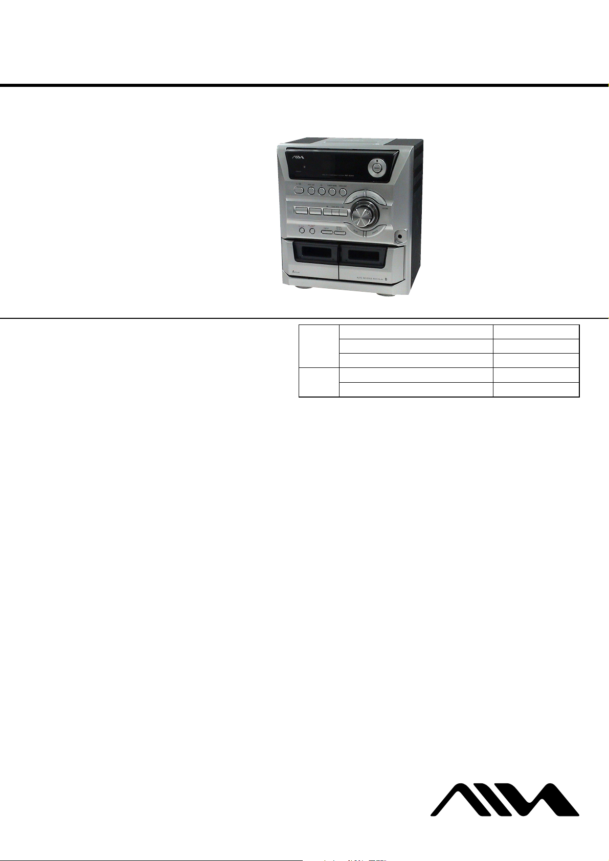
• CX-J3000 is the amplifier, CD player, tape deck and
tuner section in RBT-3000.
• CX-J3000M is the amplifier, CD player, tape deck
and tuner section in RBT-3000M.
photo: CX-J3000M
CD
Section
TAPE
Section
SPECIFICATIONS
Russian Model
CX-J3000M
E Model
CX-J3000/J3000M
Model Name Using Similar Mechanism NEW
Optical Pick-up Block Name KSM-213RDP
Optical Pick-up Name KSS-213R
Model Name Using Similar Mechanism NEW
Tape Transport Mechanism Type CWM43FR55
Amplifier section
CX-J3000
Continuous RMS power output (reference):
CX-J3000M
Continuous RMS power output (reference):
CX-J3000M
Continuous RMS power output (reference):
CX-J3000M (Chilean and Peruvian models)
Continuous RMS power output (reference):
Inputs
VIDEO/SAT IN (phono jacks):
Outputs
PHONES (stereo mini jack):
(Russian model)
(Mexican model)
25 + 25 watts (6 ohms at 1
kHz, 10% THD) measured
at AC 240 V 50/60 Hz
2 + 2 watts (6 ohms at 1
kHz, 10% THD) measured
at DC 12 V
25 + 25 watts (6 ohms at 1
kHz, 10% THD) measured
at AC 230 V 50/60 Hz
45 + 45 watts (6 ohms at 1
kHz, 10% THD) measured
at AC 127 V 60 Hz
45 + 45 watts (6 ohms at 1
kHz, 10% THD) measured
at AC 240 V 50/60 Hz
Voltage 0.775 V,
impedance 47 kilohms
Accepts headphones of 8
ohms or more
SPEAKER: Accepts impedance of 6 to
CD player section
System Compact disc and digital
Laser Semiconductor laser
Frequency response 2 Hz – 20 kHz (±0.5 dB)
Wavelength 760 – 800 nm
Signal-to-noise ratio More than 90 dB
Dynamic range More than 90 dB
Tape deck section
Recording system 4-track 2-channel, stereo
Frequency response 50 – 13,000 Hz (±3 dB),
Tuner section
FM stereo, FM/AM superheterodyne tuner
FM tuner section
Tuning range 87.5 – 108.0 MHz
Antenna FM telescopic antenna
Intermediate frequency 10.7 MHz
AM tuner section
Tuning range
2 Band type:
Mexican, Chilean and Peruvian models:
16 ohms
audio system
(λ =780 nm)
Emission duration:
continuous
using Sony TYPE I
cassettes
(50-kHz step)
530 – 1,710 kHz
(with the tuning interval
Russian model: 531 – 1,602 kHz (with the
3 Band type:
MW: 531 – 1,602 kHz
SW1: 3.200 – 7.300 MHz
SW2: 9.500 – 21.850 MHz
Antenna AM loop antenna
Antenna terminals External antenna terminal
Intermediate frequency 450 kHz
General
Power requirements
Indian and African
Russian model: 230 V AC, 50/60 Hz
Mexican model: 127 V AC, 60 Hz
Chilean and Peruvian models:
set at 10 kHz
531 – 1,710 kHz
(with the tuning interval
set at 9 kHz)
tuning interval set at 9
kHz)
(with the tuning interval
set at 9 kHz)
(with the tuning interval
set at 1 kHz)
(with the tuning interval
set at 5 kHz)
models:
220 – 240 V AC, 50/60 Hz
12 V DC
110 – 120 V or 220 – 240 V
AC, 50/60 Hz
Adjustable with voltage
selector
-
Continued on next page
-
9-879-115-01
2004H0579-1
© 2004.08
COMPACT DISC DECK RECEIVER
Sony Corporation
Personal Audio Company
Published by Sony Engineering Corporation
Page 2
CX-J3000/J3000M
Power consumption
nd CX-J3000M (
CX-J3000 a
CX-J3000M (
CX-J3000M (
Dimensions (w/h/d) incl. projecting parts and controls
Amplifier/Tuner/Tape/CD section:
Mass
CX-J3000 and CX-J3000M (Russian model):
CX-J3000M (Mexican, Chil ean and Peruvian models)
Design and specifications are subject to change
without notice.
Mexican model):
Chilean and Peruvian models):
Russian model):
70 watts
90 watts
100 watts
Approx. 270 × 300 × 294
mm
Approx. 4.8 kg
Approx. 5.5 kg
Notes on chip component replacement
• Never reuse a disconnected chip component.
• Notice that the minus side of a tantalum capacitor may be
damaged by heat.
Flexible Circuit Board Repairing
• Keep the temperature of the soldering iron around 270 ˚C
during repairing.
• Do not touch the soldering iron on the same conductor of the
circuit board (within 3 times).
• Be careful not to apply force on the conductor when soldering
or unsoldering.
CAUTION
Use of controls or adjustments or performance of procedures
other than those specified herein may result in hazardous radiation
exposure.
This appliance is classified as
a CLASS 1 LASER product.
The CLASS 1 LASER
PRODUCT MARKING is
located on the rear exterior.
SAFETY-RELATED COMPONENT WARNING!!
COMPONENTS IDENTIFIED BY MARK 0 OR DOTTED LINE
WITH MARK 0 ON THE SCHEMATIC DIAGRAMS AND IN
THE PARTS LIST ARE CRITICAL TO SAFE OPERATION.
REPLACE THESE COMPONENTS WITH SONY PARTS WHOSE
PA RT NUMBERS APPEAR AS SHOWN IN THIS MANUAL OR
IN SUPPLEMENTS PUBLISHED BY SONY.
2
Page 3
CX-J3000/J3000M
Playable discs
You can play back the following discs on this
system. Other discs cannot be played back.
List of playable discs
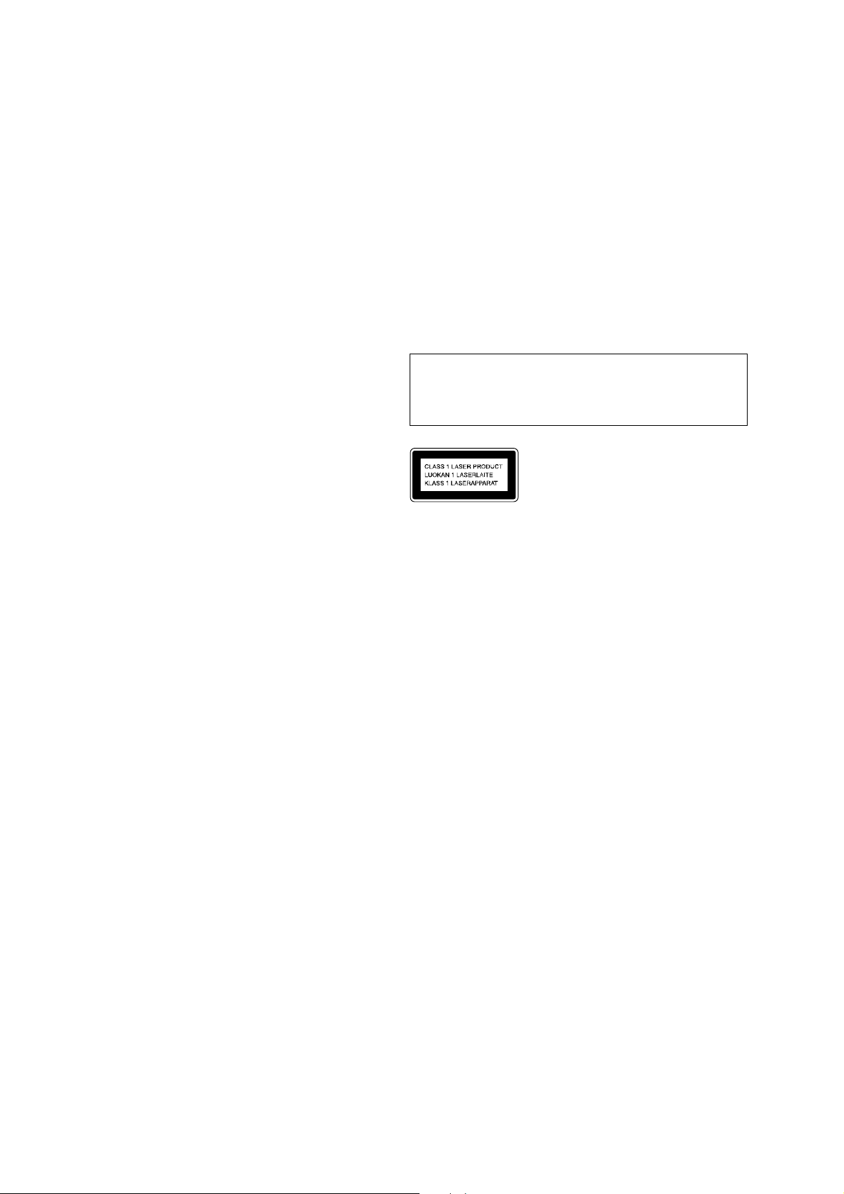
Format of discs Disc logo
Audio CDs
CD-R/CD-RW
(audio data/MP3
files*)
* CX-J3000M only
Discs that this system cannot
play
CD-ROMs
••CD-Rs/CD-RWs other than those recorded in
the following formats:
–music CD format
–MP3 format that conforms to ISO9660
Level 1/Level 2, Joliet, Romeo or Multi
2)
Session
• Discs with non-standard shapes (e.g., heart,
square, star) cannot be played on this unit.
Attempting to do so may damage the unit. Do
not use such discs.
• A disc with paper or stickers on it.
• A disc that has the adhesive, cellophane tape,
or a sticker still left on it.
1)
A logical format of files and folders on a CDROMs, defined by ISO (International Organization
for Standardization).
2)
Multi Session
This is a recording method that enables adding of
data using the Track-At-Once method.
Conventional CDs begin at a CD control area called
the Lead-in and end at an area called Lead-out. A
Multi Session CD is a CD having multiple sessions,
with each segment from Lead-in to Lead-out
regarded as a single session.
Notes on CD-R and CD-RW
• Some CD-Rs or CD-RWs cannot be played
on this system depending upon the recording
quality or physical condition of the disc, or
the characteristics of the recording device.
Furthermore, the disc will not play if it has not
been correctly finalized. For more
information, see the operating instructions for
the recording device.
• Discs recorded on CD-R/CD-RW drives may
not be played back because of scratches, dirt,
recording condition or the driver’s
1)
• CD-R and CD-RW discs recorded in packet
write format are not supported.
• CD-R and CD-RW discs that have not ended
by “closing the session” are not supported.
• The system may be unable to play MP3
format files that do not have the “.MP3”
extension.
• Attempting to play non-MP3 format files that
have the “.MP3” extension may result in noise
or malfunction.
• With formats other than ISO9660 Level 1,
Joliet and Romeo, folder names or file names
may not be displayed correctly.
• The following discs take a longer time to start
playback.
–a disc recorded with complicated tree
structure.
–a disc recorded in Multi Session.
–a disc to which data can be added (non-
finalized disc).
Music discs encoded with
copyright protection
technologies
This product is designed to playback discs that
conform to the Compact Disc (CD) standard.
Recently, various music discs encoded with
copyright protection technologies are marketed
by some record companies. Please be aware that
among those discs, there are some that do not
conform to the CD standard and may not be
playable by this product.
Cautions when playing a disc
that is recorded in Multi
Session
If the disc begins with a CD-DA session, it is
•
recognized as a CD-DA (audio) disc, and
playback continues until an MP3 session is
encountered.
If the disc begins with an MP3 session, it is
•
recognized as an MP3 disc, and playback
continues until a CD-DA (audio) session is
encountered.
The playback range of an MP3 disc is
•
determined by the tree structure of files
produced by analyzing of the disc.
A disc with a mixed CD or CD-Extra format
•
will be recognized as a CD-DA (audio) disc.
3
Page 4

CX-J3000/J3000M
TABLE OF CONTENTS
1. SERVICING NOTES ................................................... 5
2. GENERAL ...................................................................... 6
3. DISASSEMBLY
3-1. DISASSEMBLY FLOW .................................................... 8
3-2. SIDE PANEL (L/R) ............................................................ 8
3-3. TOP PANEL SECTION ..................................................... 9
3-4. OPTICAL BLOCK SECTION ........................................... 9
3-5. OPTICAL PICK-UP (KSS-213R).................................... 10
3-6. FRONT PANEL SECTION.............................................. 10
3-7. MECHANICAL DECK (CWM43FR55) ......................... 11
3-8. MAIN BOARD ................................................................ 11
4. TEST MODE ................................................................12
5. MECHANICAL ADJUSTMENTS.......................... 13
6. ELECTRICAL ADJUSTMENTS ........................... 13
7. DIAGRAMS
7-1. BLOCK DIAGRAM – SERVO SECTION – ................... 17
7-2. BLOCK DIAGRAM – TUNER SECTION – .................. 18
7-3. BLOCK DIAGRAM – AUDIO SECTION – ................... 19
7-4. BLOCK DIAGRAM
– DISPLAY/POWER SUPPLY SECTION – .................. 20
7-5. PRINTED WIRING BOARD
– CD SECTION (J3000) – ............................................... 22
7-6. SCHEMATIC DIAGRAM
– CD SECTION (J3000) – ............................................... 23
7-7. PRINTED WIRING BOARD
– CD/MP3 SECTION (SIDE A) (J3000M) –................... 24
7-8. PRINTED WIRING BOARD
– CD/MP3 SECTION (SIDE B) (J3000M) – ................... 25
7-9. SCHEMATIC DIAGRAM
– CD/MP3 SECTION (J3000M) – ................................... 26
7-10. PRINTED WIRING BOARDS
– PANEL SECTION –...................................................... 28
7-11. SCHEMATIC DIAGRAM – PANEL SECTION – ..........29
7-12. PRINTED WIRING BOARD
– MAIN SECTION – ....................................................... 30
7-13. SCHEMATIC DIAGRAM
– MAIN SECTION (1/3) – ............................................... 31
7-14. SCHEMATIC DIAGRAM
– MAIN SECTION (2/3) – ............................................... 32
7-15. SCHEMATIC DIAGRAM
– MAIN SECTION (3/3) – ............................................... 33
7-16. PRINTED WIRING BOARD – AMP SECTION – ......... 34
7-17. SCHEMATIC DIAGRAM – AMP SECTION – .............. 35
7-18. PRINTED WIRING BOARDS
– POWER SUPPLY SECTION –..................................... 36
7-19. SCHEMATIC DIAGRAM
– POWER SUPPLY SECTION –..................................... 37
8. EXPLODED VIEWS
8-1. BACK/SIDE PANEL SECTION...................................... 45
8-2. TOP PANEL SECTION ................................................... 46
8-3. FRONT PANEL (TAPE DECK) SECTION .................... 47
8-4. FRONT PANEL SECTION.............................................. 48
8-5. CHASSIS SECTION ........................................................ 49
8-6. OPTICAL PICK-UP SECTION (KSM-213RDP) ........... 50
9. ELECTRICAL PARTS LIST ................................... 51
4
Page 5
SECTION 1
SERVICING NOTES
CX-J3000/J3000M
NOTES ON HANDLING THE OPTICAL PICK-UP
BLOCK OR BASE UNIT
The laser diode in the optical pick-up block may suffer electrostatic
break-down because of the potential difference generated by the
charged electrostatic load, etc. on clothing and the human body.
During repair, pay attention to electrostatic break-down and also
use the procedure in the printed matter which is included in the
repair parts.
The flexible board is easily damaged and should be handled with
care.
NOTES ON LASER DIODE EMISSION CHECK
The laser beam on this model is concentrated so as to be focused on
the disc reflective surface by the objective lens in the optical pickup block. Therefore, when checking the laser diode emission,
observe from more than 30 cm away from the objective lens.
UNLEADED SOLDER
Boards requiring use of unleaded solder are printed with the leadfree mark (LF) indicating the solder contains no lead.
(Caution: Some printed circuit boards may not come printed with
the lead free mark due to their particular size)
: LEAD FREE MARK
Unleaded solder has the following characteristics.
• Unleaded solder melts at a temperature about 40 °C higher
than ordinary solder.
Ordinary soldering irons can be used but the iron tip has to be
applied to the solder joint for a slightly longer time.
Soldering irons using a temperature regulator should be set to
about 350 °C.
Caution: The printed pattern (copper foil) may peel away if
the heated tip is applied for too long, so be careful!
• Strong viscosity
Unleaded solder is more viscou-s (sticky, less prone to flow)
than ordinary solder so use caution not to let solder bridges
occur such as on IC pins, etc.
• Usable with ordinary solder
It is best to use only unleaded solder but unleaded solder may
also be added to ordinary solder.
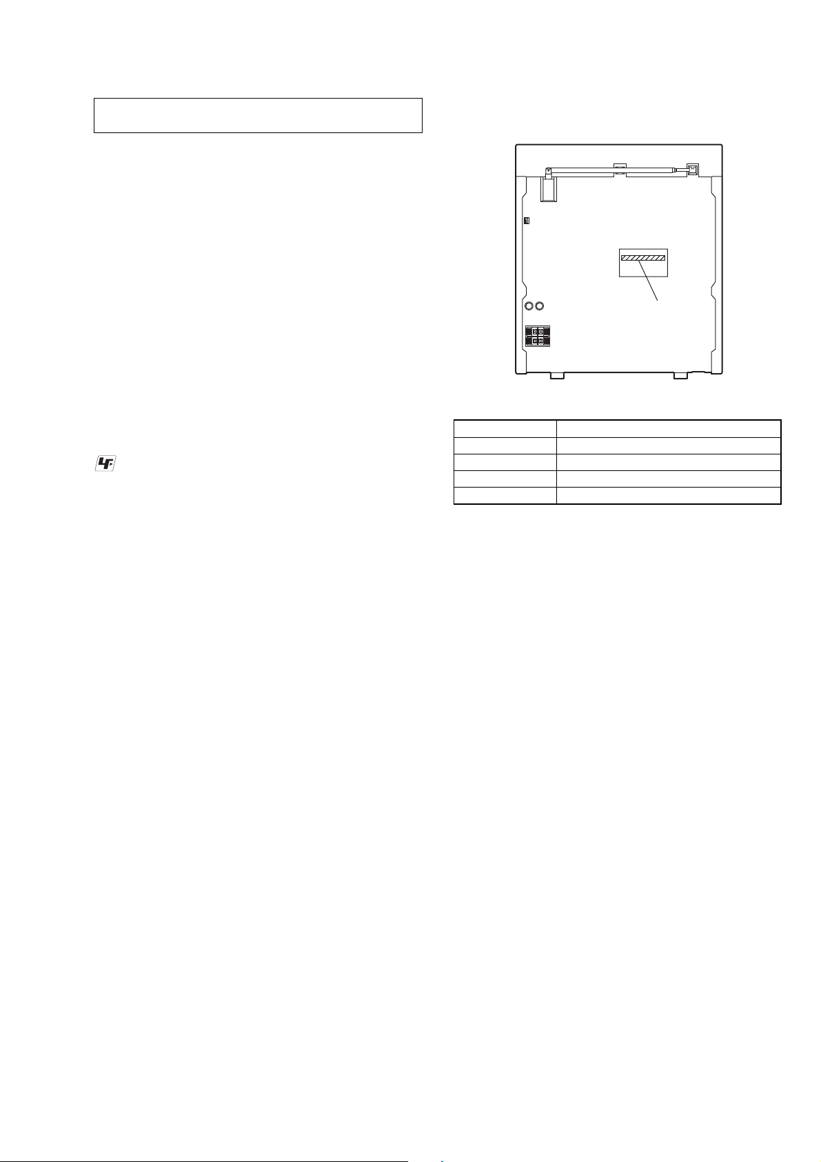
• MODEL IDENTIFICATION
– Back Panel –
Power Voltage
Indication
MODEL Power Voltage Indication
CX-J3000 AC: 220-240V ~ 50/60Hz 70W
CX-J3000M: RU AC: 230V ~ 50/60Hz 70W
CX-J3000M: E51 AC: 110-120V/220-240V ~ 50/60Hz 100W
CX-J3000M: MX ca ~ 127V 60Hz 90W
•Abbreviation
E51 : Chilean and Peruvian models
MX : Mexican model
RU : Russian model
5
Page 6
CX-J3000/J3000M
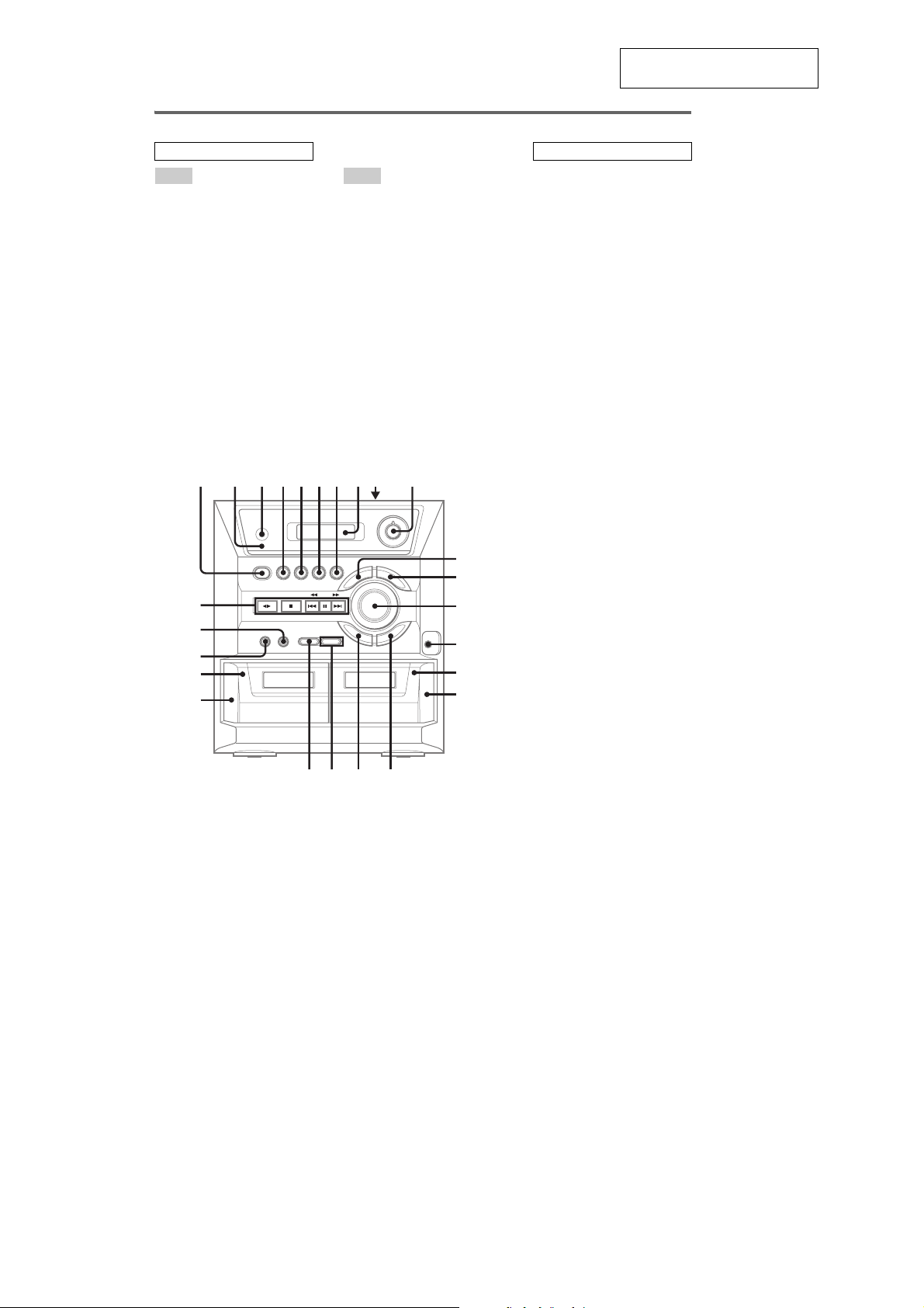
q
q
w
q
Main unit
ALPHABETICAL ORDER
A – O P – Z
ALBUM +/–
CD 5
CD SYNC wd
DANCE qj
Deck A wa
Deck B qh
DISPLAY w;
Display window 8
FLAT qk
FM MODE
i-Bass 0
134567
1)
ql
2)
ql
2 89
SECTION 2
GENERAL
PHONES jack qf
POP qs
3)
POWER
REC PAUSE/START wf
Remote sensor 3
REPEAT
ROCK qa
STANDBY indicator 2
TAPE A/B 4
TUNER/BAND 6
TUNING MODE wg
VIDEO/SAT 7
VOLUME control qd
1
2)
ql
q;
This section is extracted from
instruction manual.
BUTTON DESCRIPTIONS
4)
?/1
(power) 1
./> (go back/go forward)
wg
m/M (rewind/fast forward)
wg
x (stop) wg
X (pause) wg
nN (play) wg
Z PUSH (deck A) (open/close)
ws
Z PUSH (deck B) (open/close)
qg
Z PUSH OPEN/CLOSE (open/
close) 9
+/– (tuning) wg
1)
CX-J3000M only
2)
Except for CX-J3000M
3)
Except for CX-J3000
4)
CX-J3000 only
wg
wf
wd
ws
wa
qa
qs
qd
qf
qg
qh
k
l
;
j
6
Page 7
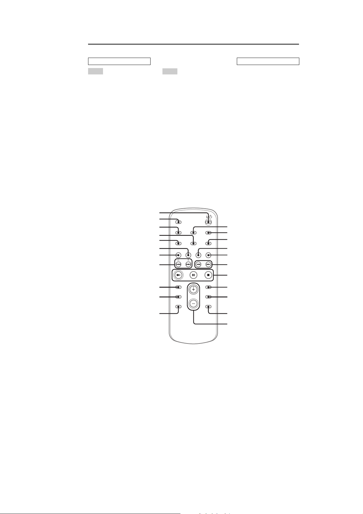
Remote control
CX-J3000/J3000M
ALPHABETICAL ORDER
A – O
ALBUM +
ALBUM –
CD qj
CLEAR qf
DISC SKIP
DISPLAY w;
ENTER 8
EQ qd
FM MODE 3
FUNCTION 5
1)
0
1)
qs
2)
9
P – Z
PLAY MODE ql
REPEAT 3
2)
SELECT
2)
SET
2
SLEEP wa
TAPE qh
TUNER BAND 4
TUNER MEMORY qk
TUNING MODE ql
VOLUME +/– qa
ws
wa
w;
ql
qk
qj
qh
qg
1
BUTTON DESCRIPTIONS
?/1 (power) ws
./> (go back/go forward)
qg
m/M (rewind/fast forward)
6
x (stop) 7
X (pause) 7
N (play) 7
+/– (tuning) qg
1)
CX-J3000M only
2)
This button cannot be used in
this system.
1
2
3
4
5
6
qf
qd
qs
7
8
9
q;
qa
7
Page 8
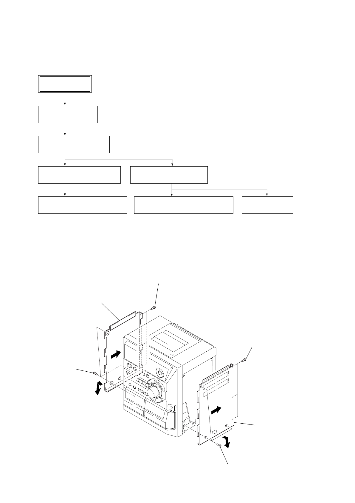
CX-J3000/J3000M
• This set can be disassembled in the order shown below.
3-1. DISASSEMBLY FLOW
SET
3-2. SIDE PANEL (L/R)
(Page 8)
3-3. TOP PANEL SECTION
(Page 9)
SECTION 3
DISASSEMBLY
3-4. OPTICAL BLOCK SECTION
(Page 9)
3-5. OPTICAL PICK-UP (KSS-213R)
(Page 10)
Note: Follow the disassembly procedure in the numerical order given.
3-6. FRONT PANEL SECTION
(Page 10)
3-7. MECHANICAL DECK (CWM43FR55)
3-2. SIDE PANEL (L/R)
5
side panel (L)
3
(Page 11)
2
three screws
(BVTP 3
3-8. MAIN BOARD
(Page 11)
×
10)
7
three screws
(BVTP 3
×
10)
1
three screws
(case 3 TP2)
4
8
side panel (R)
0
9
6
three screws
(case 3 TP2)
8
Page 9
3-3. TOP PANEL SECTION
)
)
s
6
4
connector
(CN851)
top panel section
2
1
two screws
(BVTP 3
3
FFC 14P (J3000
FFC 20P (J3000M
(CNP702)
5
terminal
(CN206)
CX-J3000/J3000M
×
10)
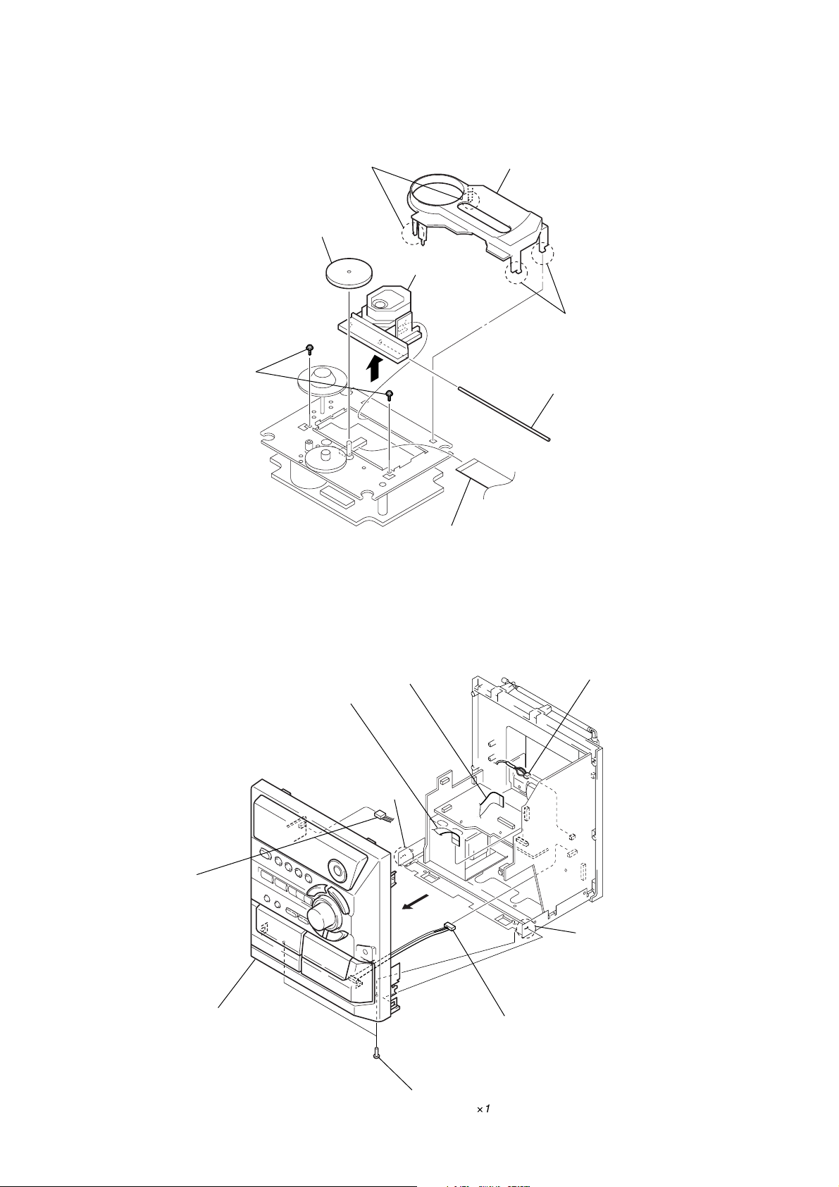
3-4. OPTICAL BLOCK SECTION
1
four screws
(BVTP 3
´
10)
5
two vibration
proof robbers
3
2
insulating sheet
screw
(PTPWH M2.6)
4
7
optical block section
6
CD cover
3
screw
(PTPWH M2.6)
5
3
two screws
(PTPWH M2.6)
two vibration
proof robber
9
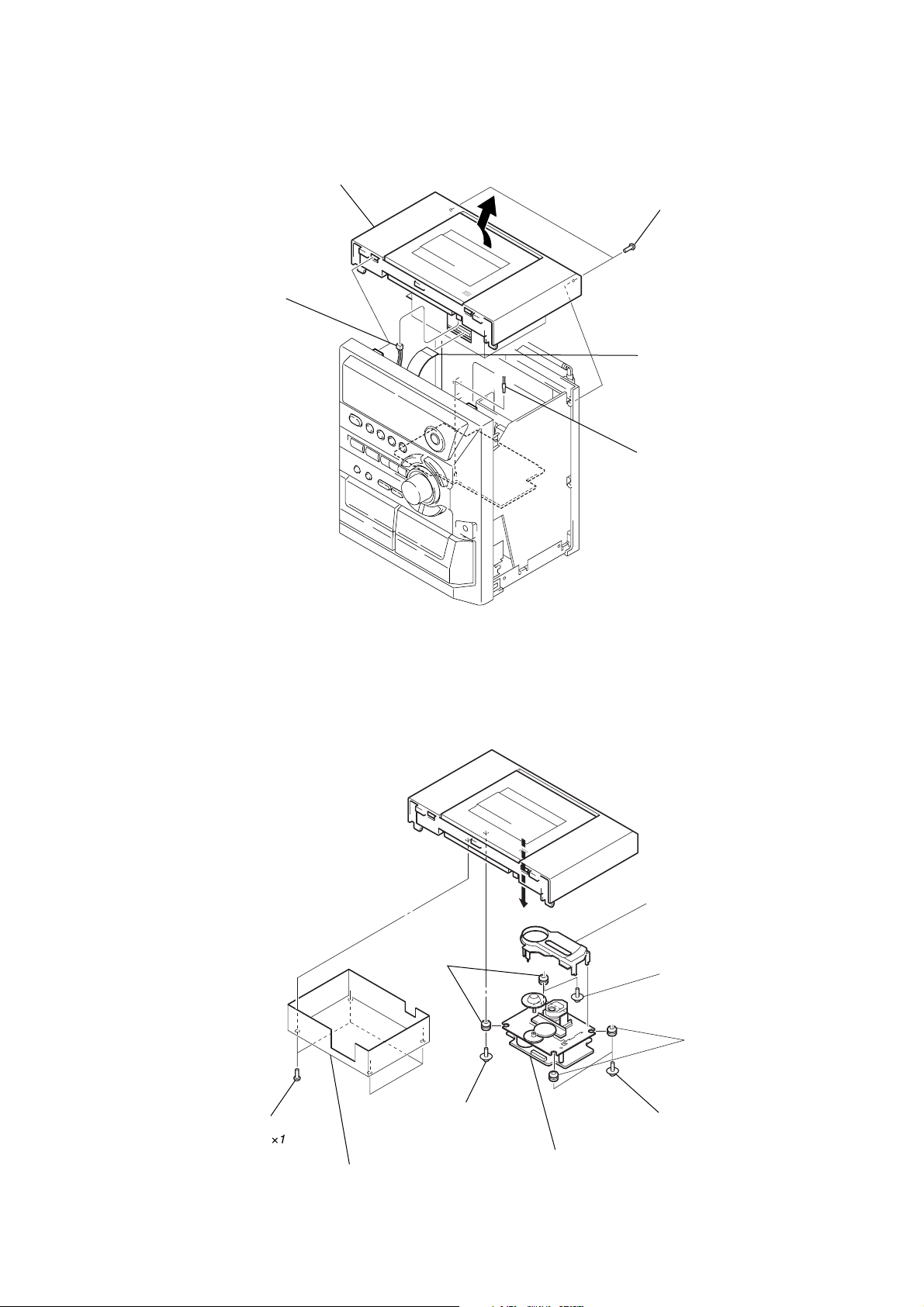
Page 10
CX-J3000/J3000M
s
r
3-5. OPTICAL PICK-UP (KSS-213R)
4 two screws (M2)
1 two claws
3 gear (B)
5
2 CD cover
8 optical pick-up
(KSS-213R)
1 two claw
6 sled shaft
7 flexible flat cable (16core) (CNP701)
3-6. FRONT PANEL SECTION
5
connector
(CN003)
9
front panel section
3
FFC13P (J3000M)
FFC15P (J3000)
(CN102)
2
6
FFC15P
(CN105)
claw
7
4
connecto
(CN301)
6
claw
connector
8
10
1
two screws
(BVTP 3
´
10)
Page 11
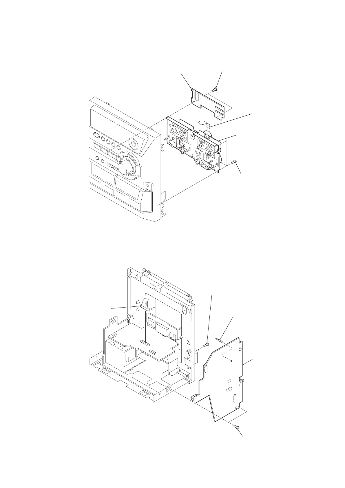
3-7. MECHANICAL DECK (CWM43FR55)
P
ck
rd
CX-J3000/J3000M
2 wire PWB
1 two screws
(BVTP3 × 10)
3 FFC 13
5 mechanical de
(CWM43FR55)
4 four screws
(BVTP3 × 10)
3-8. MAIN BOARD
1 connector
(CN201)
3 three screws
(BVTP3 × 10)
2 terminal
(CN501)
4 MAIN boa
3 two screws
(BVTP3 × 10)
11
Page 12

CX-J3000/J3000M
SECTION 4
TEST MODE
COLD RESET
• The cold reset clears all data including preset data stored in
the RAM to initial conditions. Execute this mode when
returning the set to the customer.
Procedure:
1. Press the [POWER] button to turn the power on.
2. While pressing the x button, press the [i-Bass] button and
turn the [VOLUME] knob counter-clockwise.
3. The message “RESET” is displayed and the set is reset.
GC TEST MODE
Procedure:
1. Press the [POWER] button to turn the power on.
2. While pressing the [DISPLAY] button, press the [i-Bass] button
for 5 seconds.
3. It change displays in order of version, model type and suffix
at 2 seconds interval, then the display is back to normal status.
AMP TEST MODE
Procedure:
1. In the power off status, while pressing the [i-Bass] button and
press the [POWER] button (J3000M) or connect the AC plug
(J3000) to turn the power on. Then enter the AMP test mode
and display “AMP TEST”.
2. If turn the [VOLUME] knob clockwise, it displays “VOL MAX”,
and if turn the knob counter-clockwise, it displays “VOL
MIN”.
3. To release from this mode, turn the power off.
CD REPEAT 5 LIMIT CANCEL MODE
• Number of repeat for CD playback is 5 times when the repeat
mode is “REPEAT”. This mode enables CD to repeat playback
for limitless times.
Procedure:
1. Press the [POWER] button to turn the power on.
2. In the repeat on status, while pressing the x button, press the
[CD] button to enter the CD repeat 5 limit cancel mode and
repeat mark blinks on the liquid crystal display.
3. To release this mode, press the [POWER] button to turn the
power off.
CHANGE-OVER OF AM TUNER STEP BETWEEN
9 kHz AND 10 kHz
•A step of AM channels can be changed over between 9 kHz and
10 kHz.
Procedure:
In the power off status, while pressing the [TUNER/BAND] button and press the [POWER] button to the display on fluorescent
liquid crystal display changes to “AM 530 kHz” (10 kHz step) or
“AM 531 kHz” (9 kHz step), and thus the channel step is changed
over.
FUNCTION CHANGE MODE
• Select either VIDEO or SAT of the external function input.
Procedure:
1. In the power off status, while pressing the [VIDEO/SAT] button and press the [POWER] button (J3000M) or connect the
AC plug (J3000).
2. Each time this operation is operated, it change displays in
order of “VIDEO” and “SAT”.
TC TEST MODE
Procedure:
1. In the power off status, while pressing the [TAPE A/B] button
and press the [POWER] button (J3000M) or connect the AC
plug (J3000) to turn the power on. Then enter the TC test mode
and display “TC TEST”.
2. Set the tape into the deck-B.
3. Press the > button, tape is forwarded to the last position.
Press the . button, tape is rewound to the beginning position.
4. Press the [REC PAUSE/START] button, tape is rewound to the
beginning position and recording starts.
5. In the step 4 status, press the x button, tape is rewound to the
beginning position and playing starts.
6. To release from this mode, turn the power off.
CD TEST MODE
Procedure:
1. In the power off status, while pressing the [CD] button and
press the [POWER] button (J3000M) or connect the AC plug
(J3000) to turn the power on. Then enter the CD test mode
and liquid crystal display is all turned on.
2. Press the > button to move the optical pick-up to outside
track, or . button to inside track. This time, “CD TEST” is
displayed on the liquid crystal display.
3. Press the Y button, normally playing is performed. In case
of focus on isrot able, focus seach is performed continuously.
4. Press the x button, focus seach is performed continuously
and LD is lited on. This time, “READING” is displayed on
the liquid crystal display.
5. Each time X button is pressed, traverse on/off are changed.
6. To release from this mode, turn the power off.
12
Page 13
SECTION 5
set
MAIN board
PHONES jack
(J202 or J203)
+
–
level meter
test tape
P-4-A063
(6.3 kHz, –10 dB)
MECHANICAL ADJUSTMENTS
CX-J3000/J3000M
SECTION 6
ELECTRICAL ADJUSTMENTS
PRECAUTION
1. Clean the following parts with a denatured alcohol-moistened
swab:
record/playback heads pinch rollers
erase head rubber belts
capstan idlers
2. Demagnetize the record/playback head with a head demagnetizer.
3. Do not use a magnetized screwdriver for the adjustments.
4. After the adjustments, apply suitable locking compound to the
parts adjusted.
5. The adjustments should be performed with the rated power
supply voltage unless otherwise noted.
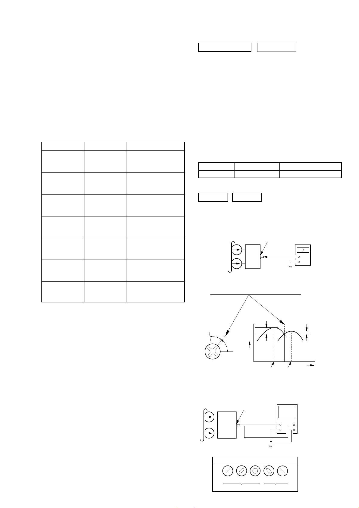
TORQUE MEASUREMENT
Mode
Tor que meter
Meter reading
3.06 N • m to 6.96 N • m
FWD
CQ-102C
31 to 71 g • cm
(0.43 – 0.98 oz • inch)
FWD
back tension
CQ-102C
0.19 N • m to 0.58 N • m
2 to 6 g • cm
(0.02 – 0.08 oz • inch)
3.06 N • m to 6.96 N • m
REV
CQ-102RC
31 to 71 g • cm
(0.43 – 0.98 oz • inch)
REV
back tension
CQ-102RC
0.19 N • m to 0.58 N • m
2 to 6 g • cm
(0.02 – 0.08 oz • inch)
6.96 N • m to 14.02 N • m
FF/REW
CQ-201B
71 to 143 g • cm
(0.98 – 1.99 oz • inch)
9.80 N • m
FWD tension
CQ-403A
100 g or more
(3.53 oz or more)
9.80 N • m
REV tension
CQ-403R
100 g or more
(3.53 oz or more)
DECK SECTION
0 dB=0.775 V
1. Demagnetize the record/playback head with a head
demagnetizer.
2. Do not use a magnetized screwdriver for the adjustments.
3. After the adjustments, apply suitable locking compound to the
parts adjust.
4. The adjustments should be performed with the rated power
supply voltage unless otherwise noted.
5. The adjustments should be performed in the order given in
this service manual. (As a general rule, playback circuit
adjustment should be completed before performing recording
circuit adjustment.)
6. The adjustments should be performed for both L-CH and RCH.
7. Switches and controls should be set as follows unless otherwise
specified.
• Test Tape
Tape Signal Used for
P-4-A063 6.3 kHz, −10 dB Azimuth Adjustment
RECORD/PLAYBACK HEAD AZIMUTH ADJUSTMENT
DECK A DECK B
Note: Perform this adjustments for both decks
Procedure:
1. Mode: Playback
2. Turn the adjustment screw and check output peaks. If the peaks
do not match for L-CH and R-CH, turn the adjustment screw
so that outputs match within 1dB of peak.
L-CH
peak
R-CH
Screw
position
peak
3. Mode: Playback
test tape
P-4-A063
(6.3 kHz, –10 dB)
set
waveform of oscilloscope
in phase 45°90°135°180
within
1dB
Output
level
MAIN board
PHONES jack
(J202 or J203)
good
L-CH
peak
wrong
R-CH
peak
oscilloscope
H
V
°
within
1dB
Screw
position
13
Page 14
CX-J3000/J3000M
3
m
4
B
7
d
s
O
a
T)
)
T)
3
m
4
er
J
f
4. After the adjustments, apply suitable locking compound to
the pats adjusted.
Adjustment Location: Playback Head (Deck A).
Record/Playback/Erase Head (Deck B).
orward
reverse
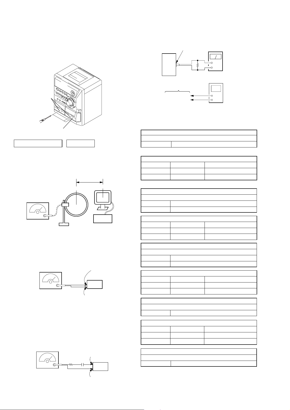
TUNER SECTION 0 dB=1 µV
[MW]
Setting:
Function : RADIO
TUNER/BAND button : MW
60 cm
loop antenna A
AM RF signal
generator
loop antenna
MAIN board
PHONES jack
(J202 or J203)
set
MAIN board
JW527 (VT)
W528 (GND)
level meter
(range: 0.5 – 5 V ac)
8 Ω
+
–
digital voltmet
•Repeat the procedures in each adjustment several times, and the
tracking adjustments should be finally done by the trimmer capacitors.
• Remove FM/SW telescopic antenna in FM and SW adjustment.
MW IF ADJUSTMENT
Adjust for a maximum reading on level meter
L514 450 kHz
<< >>: J3000 only, ( ): 10kHz step status
MW VT VOLTAGE ADJUSTMENT
Adjustment Part Frequency Display Reading on Digital Voltmeter
L503 531, (530) kHz 1.5 ± 0.1 <<1.1±0.1>> V
Confirmation 1,602, (1,710) kHz 6.3 ± 0.5 <<7.5±0.5>> V
( ): 10kHz step status
MW TRACKING ADJUSTMENT
Adjust for a maximum reading on level meter
L516 603 (620) kHz
TC503 1,404 (1,490) kHz
0% amplitude
odulation by
00 Hz signal
[FM]
Setting:
Function : RADIO
TUNER/BAND button: FM
FM RF signal
generator
5 kHz frequency
eviation by 1 kHz
ignal
utput level:
s low as possible
[SW]
Setting:
Function : RADIO
TUNER/BAND button: SW-1 or SW-2
AM RF signal
generator
14
0% amplitude
odulation by
00 Hz signal
33 Ω
MAIN board
JW535 (AN
MAIN board
JW501 (GND)
MAIN board
JW535 (AN
10 pF
set
Adjustment Part Frequency Display Reading on Digital Voltmeter
Adjustment Part Frequency Display Reading on Digital Voltmeter
set
set
SW1 VT VOLTAGE ADJUSTMENT (J3000 only)
L501 3.2 MHz 1.45 ± 0.1 V
Confirmation 7.3 MHz 6.5 ± 0.8 V
SW1 TRACKING ADJUSTMENT (J3000 only)
Adjust for a maximum reading on level meter
L504 3.2 MHz
TC502 7.3 MHz
SW2 VT VOLTAGE ADJUSTMENT (J3000 only)
L502 9.5 MHz 1.95 ± 0.1 V
Confirmation 21.85 MHz 7.5 ± 0.5 V
SW2 TRACKING ADJUSTMENT (J3000 only)
Adjust for a maximum reading on level meter
L505 15 MHz
FM VT VOLTAGE ADJUSTMENT
Adjustment Part Frequency Display Reading on Digital Voltmeter
L513 87.5 MHz 1.75 ± 0.1 V
Confirmation 108 MHz 5.8 ± 0.5 V
FM TRACKING ADJUSTMENT
Adjust for a maximum reading on level meter
L512 98 MHz
Adjustment Location: MAIN board (See page 15)
MAIN board
JW501 (GND
Page 15
Adjustment Location:
− MAIN BOARD (Component Side) −
TC503
MW Tracking Adjustment
L516
JW527
(GND)
TC502
L504
JW528
(VT)
SW1
Tr acking
Adjustment
(J3000 only)
CX-J3000/J3000M
L502
SW2 VT Voltage Adjustment (J3000 only)
L501
SW1 VT Voltage Adjustment (J3000 only)
L503
MW VT Voltage Adjustment
JW501
(GND)
JW535
(ANT)
L505
SW2 Tracking Adjustment
(J3000 only)
L513
FM VT Voltage Adjustment
L512
FM Tracking Adjustment
L514
MW IF Adjustment
J202 (J3000)
or
J203 (J3000M)
15
Page 16
CX-J3000/J3000M
CD SECTION
CD section adjustments are done automatically in this set.
In case of operation check, confirm that focus bias.
Focus Bias Check (J3000)
1. Connect the oscilloscope to TP (RF) and TP (GND) on the
CD board.
2. Insert the disc (YEDS-18). (Part No. : 3-702-101-01)
3. Press the
4. Confirm that the oscilloscope waveform is as shown in the
figure below. (eye pattern)
A good eye pattern means that the diamond shape (◊) in the
center of the waveform can be clearly distinguished.
• RF signal reference waveform (eye pattern)
VOLT/DIV: 200 mV (with the 10: 1 probe in use.)
TIME/DIV: 500 ns
When observing the eye pattern, set the oscilloscope
for AC range and raise vertical sensitivity.
Y
button.
0.85
±
0.2 Vp-p
Focus Bias Check (J3000M)
1. Connect the oscilloscope to TP (RF) and TP (VREF) on the
CD/MP3 board.
2. Insert the disc (YEDS-18). (Part No. : 3-702-101-01)
3. Press theY button.
4. Confirm that the oscilloscope waveform is as shown in the
figure below. (eye pattern)
A good eye pattern means that the diamond shape (◊) in the
center of the waveform can be clearly distinguished.
• RF signal reference waveform (eye pattern)
VOLT/DIV: 50 mV (with the 10: 1 probe in use.)
TIME/DIV: 500 ns
0.85
±
0.2 Vp-p
When observing the eye pattern, set the oscilloscope
for AC range and raise vertical sensitivity.
Adjustment Location:
− CD/MP3 BOARD (Side B) −
Adjustment Location:
− CD BOARD (Conductor Side) −
IC701
TP (GND)
TP (RF)
TP (RF)
TP (VREF)
16
Page 17
SECTION 7
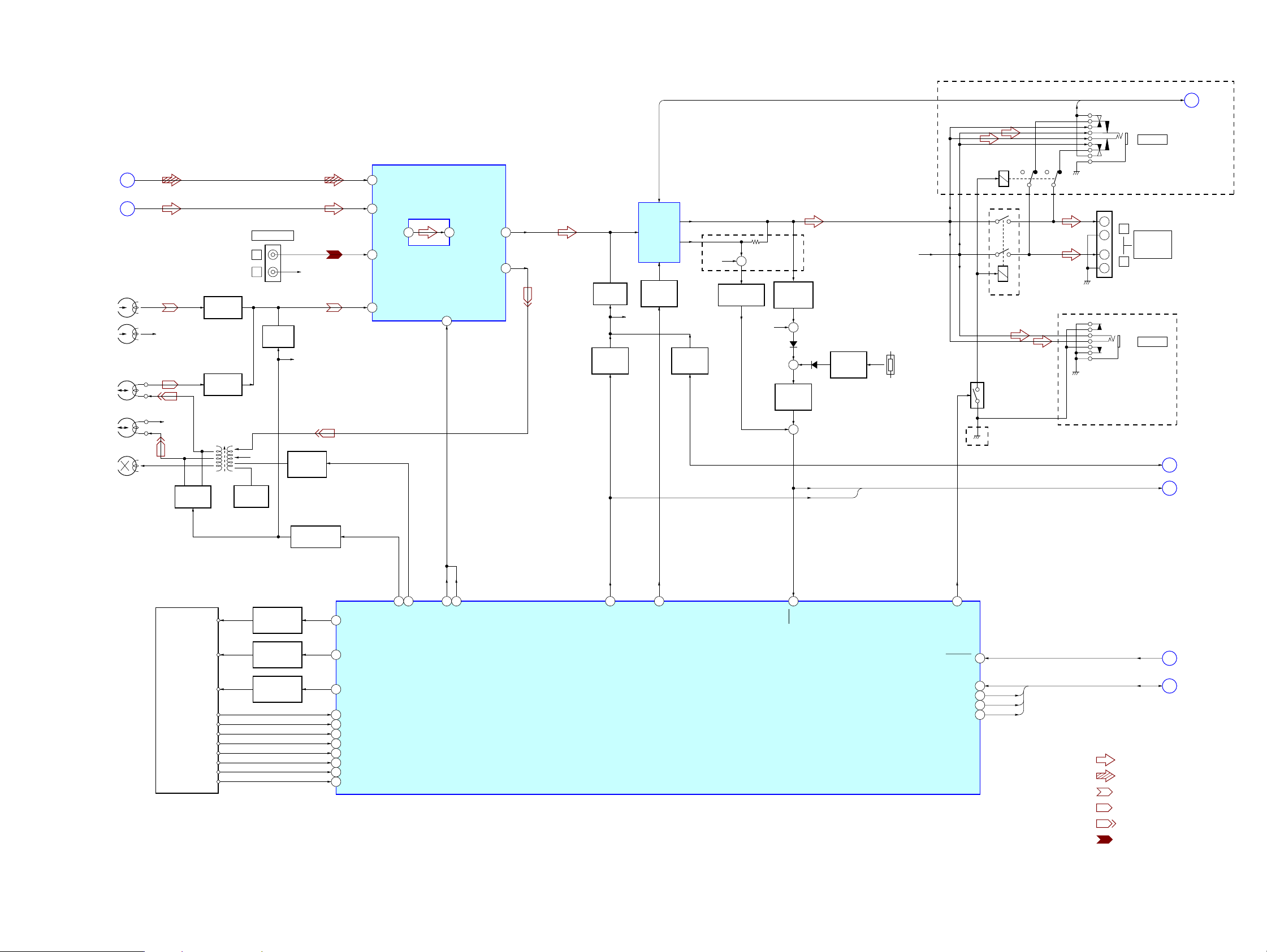
7-1. BLOCK DIAGRAM – SERVO SECTION –
CX-J3000/J3000M
DIAGRAMS
A
C
B
D
E
F
LD
PD
VREF
OPTICAL PICK-UP
BLOCK
(KSM-213RDP)
(TRACKING)
(FOCUS)
M702
(SLED)
M701
(SPINDLE)
• R-ch is omitted due to same as L-ch.
• SIGNAL PATH
M
M
: CD PLAY
A
C
B
D
E
F
LD
PD
VR
VREF
T+
T–
F+
F–
SL+
SL–
SP+
SP–
LD POWER
CONTROLLER
Q701
VREF
FIN2
FIN1
7
TIN1
9
TIN2
10
LDD
80
LDS
79
VREF
11
T+
17
T–
18
F+
12
F–
11
SL+
26
SL–
27
SP+
2
SP–
1
SLED/SPINDLE
MOTOR DRIVER,
TRACKING/FOCUS
APC
TRACKING
COIL
DRIVE
FOCUS
COIL
DRIVE
SLED
MOTOR
DRIVE
SPINDLE
MOTOR
DRIVE
COIL DRIVER
IC702
(CX-J3000)
(CX-J3000M)
PH/BH
MUTE
VREF
OPIN
TIN
FIN
SLIN
SPIN
RF
48
20
10
7
25
3
23
15
D/A
CONVERTER
TDDTD
FDD
SPDO
20
21 22 23
FD
SP
TD
FD
SL
SP
VREF
S851
CD LID OPEN/CLOSE
DETECT
EFMIN
3
AGC
HFL
PH(RFENV)
FE
TE
VREF
SLDO
SL
SLICE
LEVEL
CONTROL
CLV,CAV
CONTROL
A/D
CONVERTER,
SERVO
PROCESSOR
RF AMP,
SYSTEM SERVO PROCESSOR,
DIGITAL SIGNAL PROCESSOR
(CX-J3000)
(CX-J3000M)
IC701
S701
(LIMIT)
I_CD_LID
22
SWITCH
ERROR
CORRECTION
AUDIO CD
FRAME SYNC
DETECT,PROTECT
INSERT
EFM DECODER
GENERAL
PURPOSE
PORT
CONT1
FSEQ
DRF
67
31 72 25 66 63 61 62 49 48
9 28 3 100 5 25 41
I_CD_DRF
I_MP3_FSEQ
INTERPOLATION
MUTE
ATTENUATION
DEEMPHASIS
CONT4
RES
O_CD_RST
SYSTEM CONTROLLER
IC801 (1/3)
&
PLL
VCEC
COMMAND
INTERFACE
DICECL
O_CD_DATA
WRQ
65 64
O_CD_CE
O_CD_CLK
DO
I_CD_WRQ
8FS
DIGITAL
FILTER
&
1-bit DAC
SERIAL
OUT
EXTERNAL
AUDIO IN
CLOCK
GENERATOR
XIN
X701
16.93MHz
I_CD_DATA
O_MP3_CE/O_AMP_ON
I_MP3_INTB/I-HP
XOUT
LCHO
LPF
RCHO
DATA
DATACK
LRSY
ASDFIN
ASDACK
ASLRCK
FSX/16MIN
16MOUT
CF2
42
CD-L
A
(Page 19)
45
R-CH
7960
DATA IN
DATACK
59
58
57
56
55
52
50
99
27
80
1
LRSY
2
ADDATA
3
ADBCK
4
ADLRCK
5
CF2IN
CKOUT
9
CKIN
754
CMDOUT
73
74
CMDIN
75
CL
76
CE
INTB
77
78
RESB
MDATA0
MDATA15
23-30,33-40 60-53,50
2-5,7-10,
35-38,40-43
DQ0-DQ15
AMP-ON
HP-ON
I
MP3 DECODER,
CD-ROM DECODER,
ANTI-SHOCK
CONTROLLER
IC1001
MADRS0
I
MADRS8
18-21,24-28
B
A0-A8
SDRAM
IC1002
(Page 19)
41 44 43 45 42
16 30 31 29 15
RASB
RAS
CASLB
CASUB
LCAS
UCAS
OEB
OE
(J3000M)
WEB
WE
(J3000)
CX-J3000/J3000M
1717
Page 18
CX-J3000/J3000M
7-2. BLOCK DIAGRAM – TUNER SECTION –
L516, TC503
CN502
LOOP
ANTENNA
MW TRACKING
L516
MW ANT
TC503
(J3000)
(J3000M)
MW SWITCH
Q509
ANT501
FM/SW TELESCOPIC
ANTENNA
RF AMP
Q510
OSC
SWITCH
Q506
TU +5V
L503
MW OSC
MW VT
VOLTAGE
L512
FM RF
FM TRACKING
L513
FM OSC
FM VT
VOLTAGE
2
24
21
22
FM RF-IN
FM RF-OUT
FM-OSC
AM RF-IN
MIX-O
FM/AM FRONT END,
IF AMP, EQ
IC501
L514
MW IF
MW IF
4
CF501
BUFFER
Q514
MUTING
Q513
CF503
CF502
10
7
6
QUAD
FM IF-IN
AM IF-IN
17
IF-REQ
18
DET-O
ST.IND
R-CH
TU-L
ST-IND
C
(Page 19)
D
16
15
R-OUT
LPF213LPF1
14
12
11
L-OUT
MPX-IN
(Page 19)
L505
SW2 ANT
SW2 TRACKING
D505
L504
SW1 ANT
D506
L504, TC502
SW1 TRACKING
TC502
SW1
SWITCH
Q508
SW2 SWITCH
Q507
D501
D502
OSC
SWITCH
Q504
OSC
SWITCH
Q505
TU +5V
L502
SW2 OSC
SW2 VT
VOLTAGE
L501
SW1 OSC
SW1 VT
VOLTAGE
(J3000M)
MW OSC
Q503
SW2 OSC
Q501
SW1 OSC
Q502
BAND SELECT
SWITCH
Q516
BAND SELECT
SWITCH
Q511, 512
BAND SELECT
SWITCH
Q515
D503
D504
20
AM-OSC
OSC-O
19
LOW-PASS
FILTER
12
IF-IN
13
IF-MUT
10
AM
11
MONO BEAT
DO
DI
CL
CE
TU-DO
6
TU-DI
4
TU-CLK
5
TU-CE
3
E
(Page 19)
16
15
FM-IN
AM-IN
SW2
SW1
8
7
20
LP-OUT
X-IN
1 22
X501
4.5MHz
19
X-OUT
18
LP-IN
P-DET
9
MUTE
PLL
IC502
• R-ch is omitted due to same as L-ch.
• SIGNAL PATH
: FM
: AM (MW/SW)
(J3000)
CX-J3000/J3000M
1818
Page 19
7-3. BLOCK DIAGRAM – AUDIO SECTION –
CX-J3000/J3000M
(Page 17)
(Page 18)
L-CH
R-CH
(REC/PB/ERASE)
L-CH
R-CH
ERASE
A
C
HP301
(PB)
(DECK A)
HRPE302
(DECK B)
CD-L
TU-L
R-CH
R-CH
Q311 – 313
MUTING
PB SWITCH
Q307
PB SWITCH
Q306
L451
BIAS OSC
VIDEO/SAT IN
L
R
R-CH
BIAS OSC
Q451
J301
MUTING
Q309
R-CH
R-CH
REC BIAS
SWITCH
Q453, 454
AMP-ON, HP-ON
HP-ON
AMP-ON
INPUT SELECT,
ELECTRICAL VOLUME
IC302
CD-L
21
TU-L
23
PBO-L
6
AUX-L
19
TA-L
2
13
7
CONT
VOLI-L
OUT-L
REC-L
18
28
MUTING
Q251
MUTING
CONTROL
Q253
POWER AMP
R-CH
IC201
(J3000)
IC202
(J3000M)
(J5000V)
STANDBY
SWITCH
Q254
POWER ON
MUTING
Q104
R-CH
Q204, 205, 207
+
DC DETECT
R-CH
OVER LOAD
DETECT
Q201
D204
PROTECT
DETECT
Q203
(J3000M)
R-CH
+
D205
THERMAL
+
DETECT
Q206
TH202
RY201
RY202
(J3000M)
RELAY
DRIVE
Q210
+
–
+
–
L
R
J202
PHONES
J201
SPEAKER
IMPEDANCE
USE 6Ω
J203
PHONES
(J3000M)
B
(Page 17)
(J3000)
+
(J3000)
I-PROTECT
O-POWER
P-ON MUTING
I-PROTECT,
O-POWER
(Page 20)
G
(Page 20)
F
TAPE MECHANISM
DECK BLOCK
CAP-MT
A-SOL
B-SOL
A-PHOTO
A-HALF
A-MODE
B-PHOTO
B-HALF
B-MODE
REC-FWD
REC-REV
CAPSTAN/REEL
MOTOR DRIVE
Q459, 460
PLUNGER DRIVE
(DECK A)
Q456, 458
PLUNGER DRIVE
(DECK B)
Q455, 457
REC/PB SWITCH
Q314, 315
O_MOTOR
40
O_A_SOL
38
O_B_SOL
39
I_A_PHOTO
31
I_A_HALF
32
I_A_MODE
30
I_B_PHOTO
34
I_B_HALF
35
I_B_MODE
36
I_REC_FWD
33
I_REC_REV
37
42
41
O_PB2
O_BIAS
97
98
O_FUNC_CLK
O_FUNC_DATA
94
O_MUTE
SYSTEM CONTROLLER
95
O_POWER
IC801 (2/3)
19
I_PROTECT
96
O_SP_ON
I_ST_IND
I_TU_DATA
O_TU_DATA
O_TU_CLK
O_TU_CE
93
TU-DO
7
TU-DI
6
TU-CLK
8
TU-CE
2
ST-IND
D
(Page 18)
(Page 18)
E
• R-ch is omitted due to same as L-ch.
• SIGNAL PATH
: FM
: CD PLAY
: TAPE PLAY (DECK A)
: TAPE PLAY (DECK B)
: TAPE REC
: AUX IN
CX-J3000/J3000M
1919
Page 20
CX-J3000/J3000M
7-4. BLOCK DIAGRAM – DISPLAY/POWER SUPPLY SECTION –
O_TU_ON
87
LCD801
LIQUID
CRYSTAL
DISPLAY
D812 – 817
LCD
BACK LIGHT
D802
i-Bass
D801
STANDBY
REMOTE CONTROL
RECEIVER
IC803
VOLUME
S801 – 812, 814, 815, 817, 818, 820 – 822 (J3000)
ROTARY ENCODER
S813
S802 – 812, 814 – 819, 821, 822 (J3000M)
LED DRIVE
Q804
LED DRIVE
Q805
LED DRIVE
Q806
S0 – S33
56 – 79
44 – 53,
COM0 – COM3
83 – 86
O_BACK_LIGHT
92
O_LED_S_BASS
91
O_LED_STANDBY
43
I_REM
29
I_VOL_ENC
23
I_KEY1,
I_KEY2
24, 25
SYSTEM CONTROLLER
IC801 (3/3)
I_POWER_DN
O_CD_ON
RES
88
V1
82
V2
81
V3
80
11
18
SW +2.6V
+2.6V
REGULATOR
Q156
SW +5V
SW +3.3V
CD +7V
SW +2.6V, SW +3.3V,
SW +5V, SW +7V
TU +5V
TUNER ON
SWITCH
Q518, 519
+5V
REGULATOR
IC151
+3.3V
REGULATOR
Q157, 158
CD/VCD ON
SWITCH
Q155
LOW VOLTAGE
DETECT
Q160
RESET SWITCH
Q803
REGULATOR
B+ SWITCH
Q154
OVER CURRENT
DETECT
Q159
VT B+
RY B+
VCC +3.3V
VOLTAGE
DETECT
IC802, Q807
B+ 3.3V
+5V
Q517
SW +7V
SW +9V
B+ SWITCH
Q520
D166
D805
D807
D809
+7V
REGULATOR
Q151 – 153
+9V
REGULATOR
Q101 – 103
B+ SWITCH
Q209
+4V
REGULATOR
Q801, 802
PROTECT SWITCH
Q208
O-POWER
I-PROTECT
O-POWER,
I-PROTECT
(Page 19)
F
F004
(J3000)
J001
DC IN 12V
–
+
CX-J3000/J3000M
X801
8.64MHz
J002
(AC IN)
(J3000M)
- AC
G
(Page 19)
(J3000M)
AMP B+
AMP B–
O_CF2
16
15
I_CF1
I_OP_BATT
21
UNREG
(J3000)
RECT
D155 – 158
RECT
D151 – 154
RECT
D104, 105
POWER TRANSFORMER
PT001 (Chilean, Peruvian)
PT002 (EXCEPT Chilean, Peruvian)
F001
F002
F003
(EXCEPT Chilean, Peruvian)
S2
VOLTAGE
SELECTOR
(Chilean, Peruvian)
S001
POWER
P-ON MUTING
2020
Page 21
CX-J3000/J3000M
B
d.
B
d.
B
d.
B
)
•NOTE FOR PRINTED WIRING BOARDS AND SCHEMATIC DIAGRAMS
Note on Printed Wiring Board:
• X : parts extracted from the component side.
• Y : parts extracted from the conductor side.
• W : indicates side identified with part number.
• f : internal component.
• : Pattern from the side which enables seeing.
(The other layers' patterns are not indicated.)
Caution:
Pattern face side: Parts on the pattern face side seen from
(Side B) the pattern face are indicated.
Parts face side: Parts on the parts face side seen from
(Side A) the parts face are indicated.
Caution:
Pattern face side: Parts on the pattern face side seen from
(Conductor Side) the pattern face are indicated.
Parts face side: Parts on the parts face side seen from
(Component Side) the parts face are indicated.
• Indication of transistor.
C
Q
E
Q
CE
Q
CE
These are omitte
These are omitte
These are omitte
Note on Schematic Diagram:
• All capacitors are in µF unless otherwise noted. pF: µµF
50 WV or less are not indicated except for electrolytics
and tantalums.
• All resistors are in Ω and 1/
specified.
f
•
• 2 : nonflammable resistor.
• 5 : fusible resistor.
• C : panel designation.
Note:
The components identified by mark 0 or dotted line with
Replace only with part number specified.
• A : B+ Line.
• B : B– Line.
•Voltages and waveforms are dc with respect to ground un-
•Voltages are taken with a VOM (Input impedance 10 MΩ).
•Waveforms are taken with a oscilloscope.
• Circled numbers refer to waveforms.
• Signal path.
•Abbreviation
: internal component.
mark 0 are critical for safety.
der no-signal conditions.
– CD and CD/MP3 Section –
no mark : CD PLAY
– MAIN Sections (3/3) –
no mark : FM
<< >> : MW
(): SW-1
[]: SW-2
– Other Sections –
no mark : TUNER
(): CD PLAY
[]: TAPE PLAY
{}: TAPE REC
Voltage variations may be noted due to normal production
tolerances.
Voltage variations may be noted due to normal production
tolerances.
F : FM
f : AM (MW/SW)
E : TAPE PLAY (DECK A)
d : TAPE PLAY (DECK B)
G : TAPE REC
J : CD PLAY
L : VIDEO
j : AUX IN
E51 : Chilean and Peruvian models
MX : Mexican model
RU : Russian model
4
W or less unless otherwise
• Circuit Boards Location
POWER-SW board
(J3000M)
ACK LIGHT board
PT board
AC INLET board
(J3000)
PANEL board
CD/MP3 board (J3000M
CD board (J3000)
AMP board
MAIN board
CX-J3000/J3000M
2121
Page 22
CX-J3000/J3000M
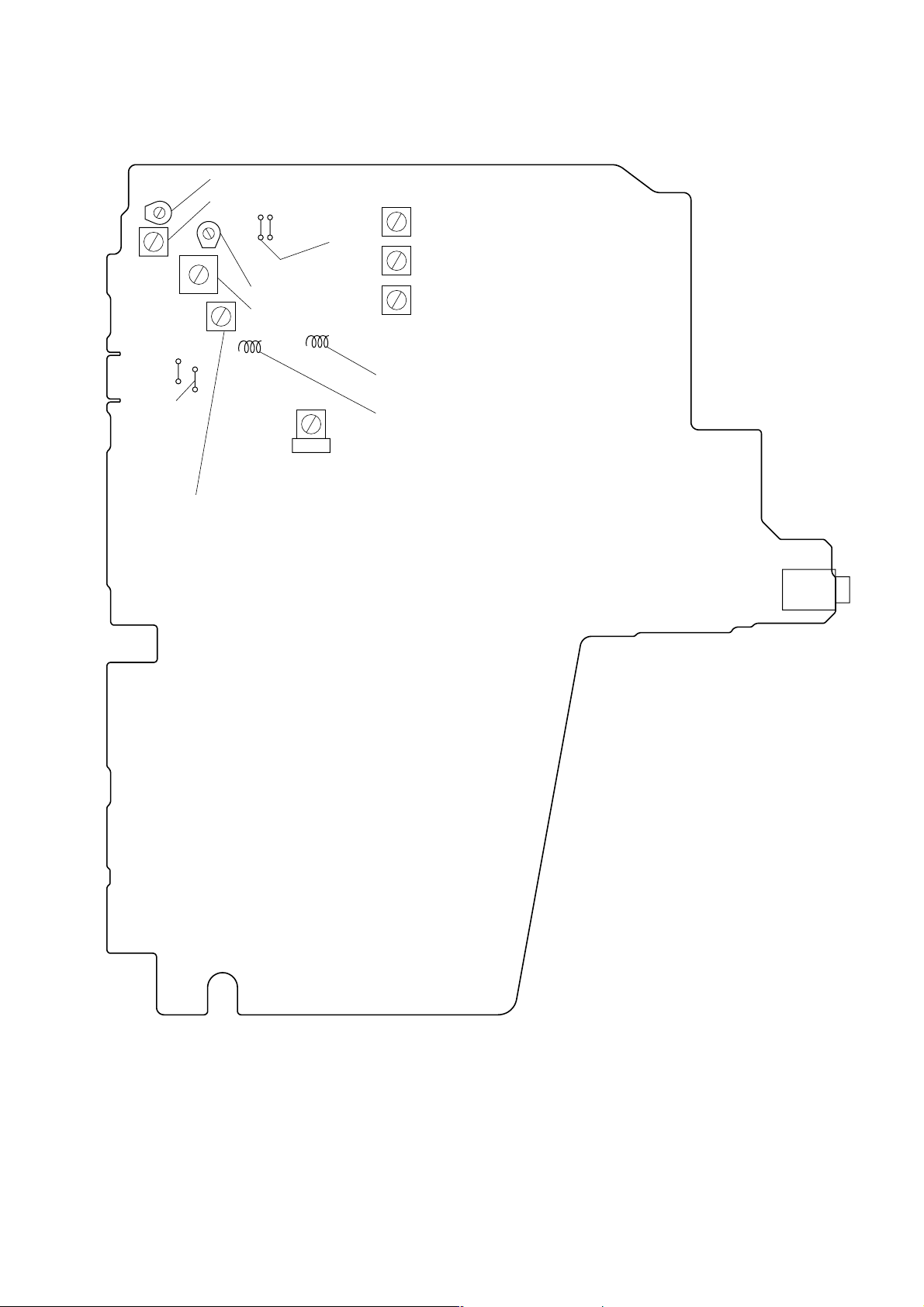
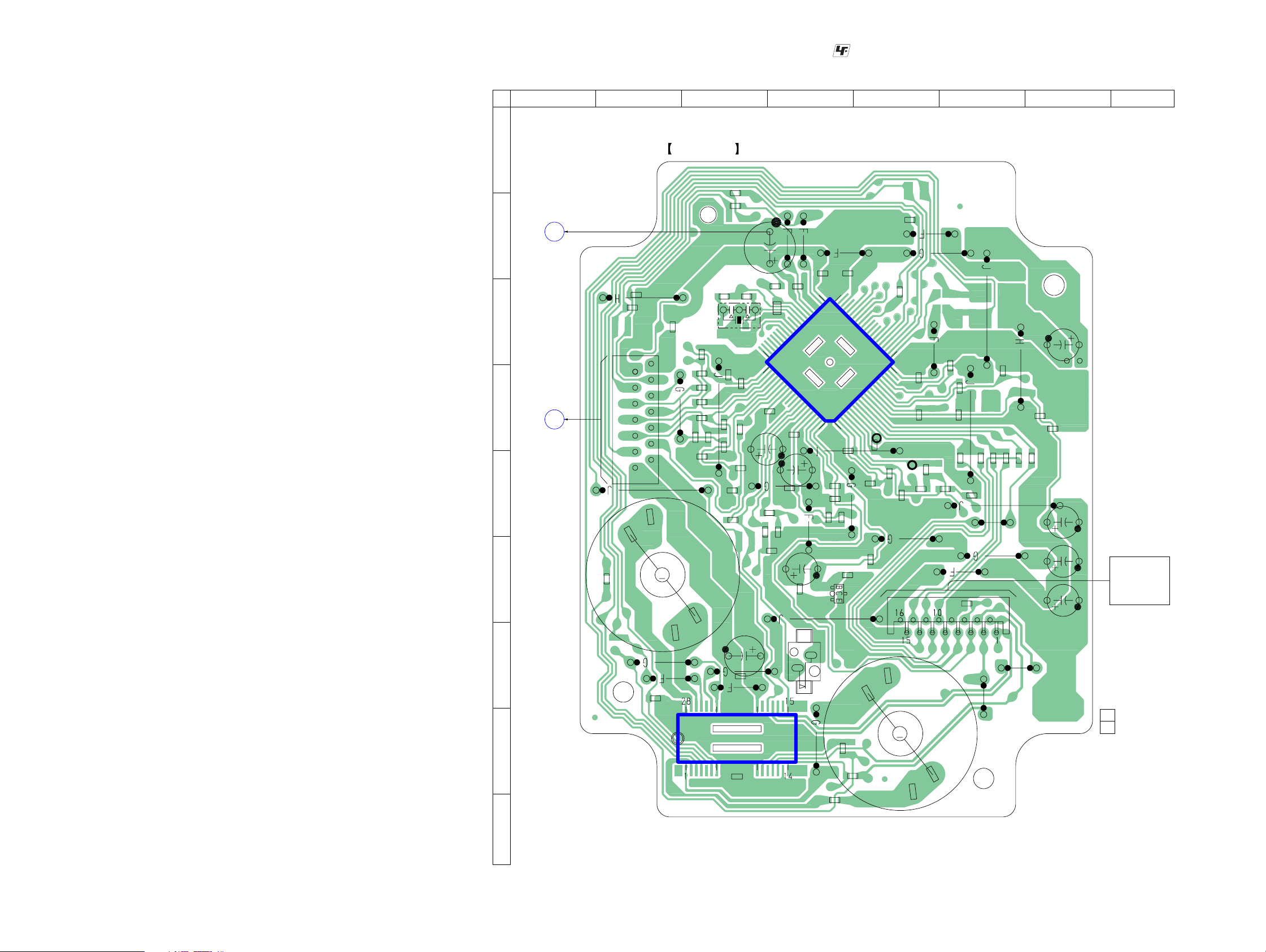
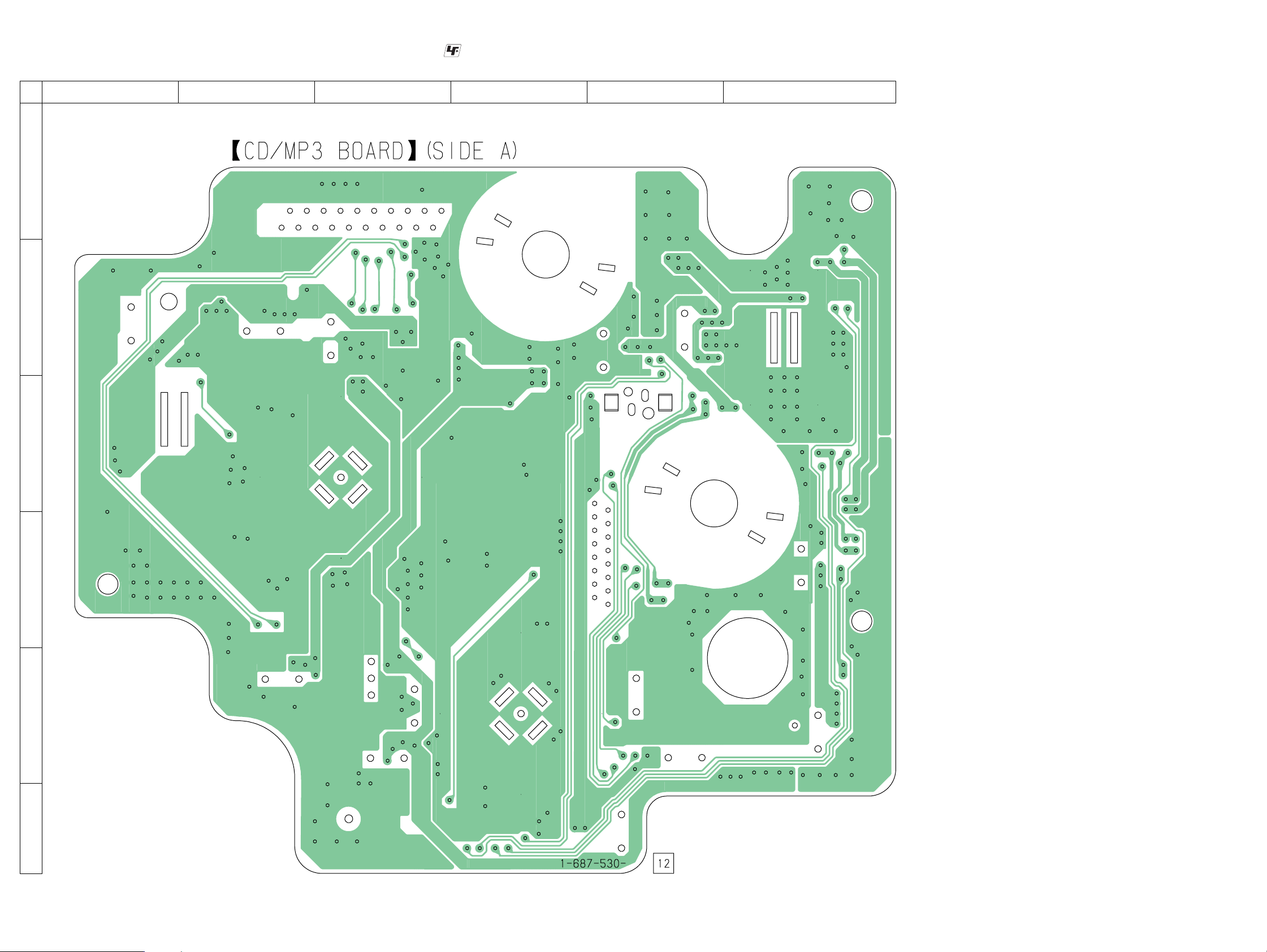
7-5. PRINTED WIRING BOARD – CD SECTION (J3000) – • : Uses unleaded solder. • See page 21 for Circuit Boards Location.
21 3 4 5 6 7
JW730
14
2
M702
CD BOARD
L706
JW729
C724
JW728
M
C722
R716
R718
R717
R719
C723
C725
R715
R714
JC704
C720
C721
JW727
R720
R721
R731
C726
R724
R732
X701
R722
60
61
C747
JW724
R725
FB701
C745
R726
C728
C717
C729
C735
C730
JW701
C716
C744
C746
C702
R707
JW702
C711
IC701
80
JW723
R729
R730
R728
Q701
JW703
C709
4041
1
C703
C701
JW722
R727
C743
JW726
C731
JW725
C751
TP
(GND)
R708
R723
21
20
C704
C727
C742
C734
TP
(RF)
JW712
R711
CNP701
JW705
JW707
C705
R710
C708
JC703
C736
R704
R709
JW714
JW708
R702
R712
JW706
R703
JW711
JW713
C707
R705
JW710
C732
JW709
C739
C738
R701
R706
C706
C750
C733
A
B
F
AMP
BOARD
CN206
(Page 34)
C754
C755
C
CNP702
13
D
A
PANEL
BOARD
CN803
(Page 28)
E
F
1
R743
(SLED)
8
OPTICAL
PICK-UP
BLOCK
(KSM-213RDP)
CX-J3000/J3000M
JW716
JW715
1-688-377-
11
(11)
G
JW720
JW719
R744
C740
C741
JW718
JW721
IC702
H
(LIMIT)
JW717
S701
JC702
R741
JC701
M701
(SPINDLE)
M
I
2222
Page 23

7-6. SCHEMATIC DIAGRAM – CD SECTION (J3000) – • See page 27 for Waveforms. • See page 38 for IC Block Diagrams.
C726
C725
C724
C723
C722
C721
C720
S701
(LIMIT)
R724
47k
C750
C751
0.1
C742
100
0.1
10V
C745C743 R731
100
0.10.1 2.2k
10V
R729R730
2201k
C744
0.1
C730 R728
0.1 10k
C747C746
100
10V
R727
2.2k
C729
1
R726 R725
680 680
8
7
2
4
7
.0
C
0
1000p
1000p
22p
0.01
CX-J3000/J3000M
S4
S5
S6
S8
S7
S9
S10
0
0
k
0
0
1
1
1
1
0
2
2
2
2
7
7
7
R
R
R
22p
22p
22p
k
k
k
00
1
1
1
1
6
7
8
1
1
1
19
7
7
7
7
R
R
R
R
(KSM-213RDP)
M702
(SLED)
M701
(SPINDLE)
CNP701
VREF
VCC
E
D
A
B
C
F
GND
LD
VR
PD
F+
T+
T-
F-
SL+
SL-
SP+
SP-
C704
22p
R709
22k
R710
16P
47k
R701
R702
15k
R703
15k
R704
15k
R705
15k
47k
R706
C739
0.1
100
R712
K1
K2
K3
K4
GND
SP-
0
2
0
7
C
J
KTN2907AS
AUTOMATIC
POWER
CONTROL
A4
SL-
SL+
SLIN
RST
SP+
SPIN
R743
6.8k
A1
R707
10
Q701
-RTK
VCC
VCC
(SLIN)
REG-B
VREF
REGO
(FIN)
GND
MUTE
TIN
4
k
4
0
7
0
R
1
A2
A3
1000p
C738
0.1
C702
47
10V
C732
100
10V
C733
100
10V
C701
K1
K4
F-
F+
FIN
T-
T+
(TIN)
K2
K3
4.7k
C703
C705
0.1
4700p
C706
1 50V
C707
1
C708
C736
100p
4700p
NC
FOCUS/TRACKING
OPIN
COIL DRIVE,
SPINDLE/SLED
MOTOR DRIVE
OPOUT
GND
0
1
70
JC
BA5826FP-E2
R741
6.8k
IC702
R708 C731
10k 0.047
R711
330
RF
VC
C734
4700p
FE
TE
JC703
0
TX TY
SLCO
SLCIST
EFMIN
RF
RFVDD
RFVSS
FIN1
FIN2
TIN1
TIN2
VREF
REFI
FE
TEC
TE
RFMON
JITTC
ADAVDD
ADAVSS
TDO
FR
LDS
LDD
SPDO
FDO
Y
P
S
FY
X
FX
P
S
A3
A1
VVSS
PDO1
PDO2
VVDD
PCKIST
RF AMP,FOCUS/TRACKING SERVO,
CONT5
CONT4
GPDAC
SLDO
SLY
SLX
A2
A4
CONT2
CONT1
DIGITAL SIGNAL PROCESSOR,
CLV SERVO,D/A CONVERTER
IC701
LC78646E
V/*P
DEFECT
SBCK/FG
SBCK/CONT6
C727 R723
1000p 100
DRF
VSS
VDD5
CONT3
MONI3
MINI2
MONI1
FSEQ
S1
*RES
MONI4
*WRQ
MONI5
DO
(3.3V)VSS
DI
VDD
CL
DATACK
ASDFIN
ASDACK
ASLRCK
16MOUT
FSX/16MIN
DOUT
CE
DATA
LRSY
EFLG
C2F
XVSS
XIN
XOUT
XVDD
RVDD
RCHO
RVSS
LVSS
LCHO
LVDD
TEST
C717
R732
0.01
C709
0.1
1M
JC704
FB701
C735
1000
6.3V
X701
16.9344MHz
1K
C755
0.01
R-CH
S3
R715
150
C716
0.01
C711
0.01
L-CH
S2
C754
R714
0.01
150
L706
S1
S10
S7
S8
S5
S4
S6
S9
S3
S2
CNP702
CD6.0V
CD R-OUT
CD L-OUT
CD 3.3V
P.GND
DOUT
D.GND
14P
FSEQ
DRF
WRQ
CL
CE
DIN
XRT
PANEL
BOARD
CN803
(Page 29)
F
AMP
BOARD
CN206
(Page 35)
CX-J3000/J3000M
C741
0.1
C740
470
10V
The components identified by mark 0 or dotted
line with mark 0 are critical for safety.
2323
Replace only with part number specified.
Page 24
CX-J3000/J3000M
7-7. PRINTED WIRING BOARD – CD/MP3 SECTION (SIDE A) (J3000M) – • : Uses unleaded solder. • See page 21 for Circuit Boards Location.
1 2 3 4 5 6
A
B
C
D
E
F
CX-J3000/J3000M
2424
Page 25
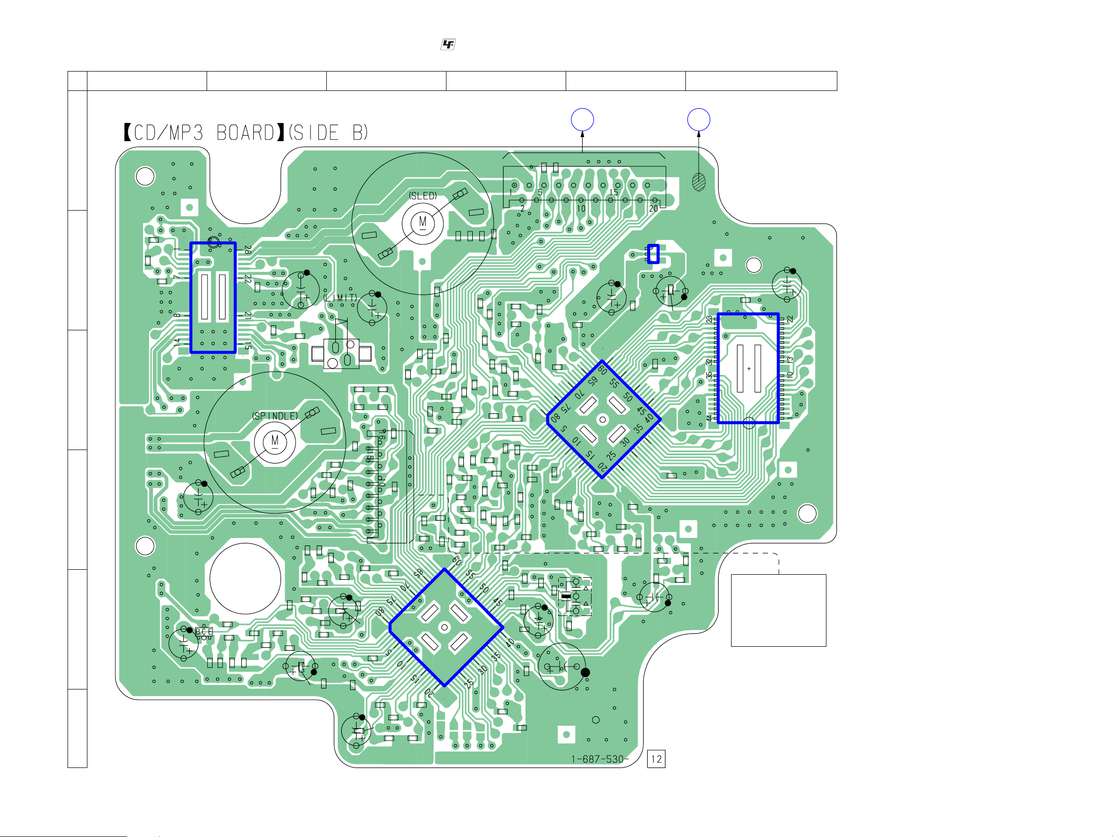
7-8. PRINTED WIRING BOARD – CD/MP3 SECTION (SIDE B) (J3000M) – • : Uses unleaded solder. • See page 21 for Circuit Boards Location.
CX-J3000/J3000M
A
B
C
D
E
F
1 2 3 4 5
PANEL BOARD
B
CNP702
R1074
C1001
R1080
FB1002
R1005
C1066
C767
C733
C732
R766
C756
R1077
C1074
FB1001
R734
R765
C730
C722
C731
R1068
C737
C734
C1043
R1073
C1044
FB701
C729
C1010
C1011
R1017
X701
R713
C1042
IC1001
R1081
R1019
R1020
R744
R712
R743
C704
C723
Q701
R707
C705
R710
R709
IC702
R708
R759
C711
C712
C747
R753
M
701
R711
C710
C713
C748
R760
C707
R704
R726
C708
R730
R757
C744
R764
R727
R729
C706
S701
R702
C743
R755
R725
R763
C709
C740
R758
R756
R728
C715
C703
R706
C714
C701
C702
R724
C746
C717
R705
R703
C716
C718
R745
C742
C719
M
R716
R701
CNP701
C721
C720
702
C754
R720
C763
R717
C745
R719
R723
C753
C761
R718
C741
C750
R1001
C762
FB707
FB706
R731
R721
C751
R1002
C1069
C1068
C764
R733
R732
IC701
FB705
C1058
R722
R1079
R1003
R1004
C1067
R735
R1075
R1076
C1057
R1078
R736
R737
FB703
R740
FB702
C1059
C1056
C1070
C760
C766
FB704
CN802
(Page 28)
C1013
C1012
R1018
IC1003
1
3
C1110
C1031
C1037
R1082
R762
R715
C1014
C1030
R714
G
C1029
R761
6
AMP BOARD
CN206
(Page 34)
C1055
IC1002
OPTICAL
PICK-UP
BLOCK
(KSM-213RDP)
C1054
CX-J3000/J3000M
2525
Page 26

CX-J3000/J3000M
7-9. SCHEMATIC DIAGRAM – CD/MP3 SECTION (J3000M) – • See page 27 for Waveforms. • See page 38 for IC Block Diagrams.
(KSM-213RDP)
CNP701
S701
R745
R701
R702
R703
R704
R705
R706
R755
R756
R757
R758
C701
C715
C718
C711
C712
C702
C703
C716
C707
C740
R759
C723
C710
C721
R707
C706
C717
C719C720
R728 R727
Q701
C705
C713R711R708R710R709
C714
C743
R725
R763
C741
C750
C742
IC701
R740
C754
C753
R724
R716
R717
R718
R719
R731
R722
R721
R720
C745
C751
R723
R734
R733
R732
15
C737
14
FB701
R715
R714
IC B/D
C722
R766
R765
R713
C733
C732
C730
C729
R762
C760
C761
C762
C763
C764
C766
R735
R736
R737
FB703
C767
R761
4701010V
1000 6.3V
X701
C1066
C1067
C1068
FB704
R1001
C1012
R1002
R1003
R1004
R1005
FB1001
R1081R1017
C1011
C1069
C1074
FB1002
C1010
C1070
R1018R1082
C1056
C1001
C1057
C1058
IC B/D
R1019
R1020
C1014
R1080
C1013
R1078
R1079
16
R1077
R1076
R1075
R1074
R1073
IC1001
C1044
C1037
R1068
C1059
IC1003
C1110
C1042
C1043
C1031
C1030
C1029
C709
C746
C744
R729R730C708
C704
R726
R764
11
12
13
PANEL
BOARD
CN802
(Page 29)
AMP
BOARD
CN206
(Page 35)
CNP702
SL704
SL703
SL702
SL701
B
C734 C731
FB702
FB705
FB706
G
FB707
M702
M701
R743
R712
R744
C756
C747
C748
R760
R753
IC702
C1054
C1055
IC1002
IC B/D
CX-J3000/J3000M
The components identified by mark 0 or dotted
line with mark 0 are critical for safety.
Replace only with part number specified.
2626
Page 27

• Waveforms
CX-J3000/J3000M
– CD Board (J3000 only) –
IC701 4 (RF)
1
(CD play mode)
0.65 to
1.05Vp-p
500 mV/DIV, 500 ns/DIV
IC701 qd (FE)
2
(CD play mode)
Approx.
90 mVp-p
50 mV/DIV, 500 ns/DIV
IC701 qg (TE)
3
(CD play mode)
– CD/MP3 Board (J3000M only) – – PANEL Board –
IC701 4 (RF)
qa
(CD play mode)
500 mV/DIV, 500 ns/DIV
IC701 qd (FE)
qs
(CD play mode)
50 mV/DIV, 500 ns/DIV
IC701 qg (TE)
qd
(CD play mode)
0.65 to
1.05Vp-p
Approx.
100 mVp-p
– MAIN Board –
IC801 qh (O_CF2)
wa
1 V/DIV, 50 ns/DIV
L451 6, 7
ea
(REC mode)
117 ns
2.9 Vp-p
20 mV/DIV, 500 ns/DIV
IC701 rk (XOUT)
4
(CD play mode)
59 ns
2 V/DIV, 20 ns/DIV
Approx.
60 mVp-p
4.4 Vp-p
50 mV/DIV, 500 ns/DIV
IC701 rk (XOUT)
qf
(CD play mode)
59 ns
2 V/DIV, 20 ns/DIV
IC701 t; (FSX/16MIN (I))
qg
(CD play mode)
60 ns
2 V/DIV, 50 ns/DIV
IC1001 7 (CKIN (I))
qh
(CD play mode)
Approx.
100 mVp-p
6.0 Vp-p
6.0 Vp-p
20 V/DIV, 5 µs/DIV
L451 5
es
(REC mode)
10 V/DIV, 5 µs/DIV
L451 3
ed
(REC mode)
IC502 ws (X-OUT)
ef
53.2 Vp-p
13.3 µs
28.0 Vp-p
13.3 µs
13.0 Vp-p
13.3 µs
5 V/DIV, 5 µs/DIV
CX-J3000/J3000M
60 ns
2 V/DIV, 50 ns/DIV
7.0 Vp-p
3.8 Vp-p
223 ns
1 V/DIV, 100 ns/DIV
2727
Page 28

CX-J3000/J3000M
7-10. PRINTED WIRING BOARDS – PANEL SECTION – • : Uses unleaded solder. • See page 21 for Circuit Boards Location.
1 2 3 4 5 6 7 8 9 10
BACK LIGHT BOARD
2
1
A
W801
D812
D813
PANEL BOARD
B
D802
JW928
JW929
JW930
D802, S806
i-BASS
C
JW813
JW814
JW815
JW816
JW817
JW818
D
L
MAIN
BOARD
CN105
(Page 30)
E
F
H
AMP
BOARD
CN102
(Page 34)
CN805
2
14
JW819
1
15
JW932
JW826
(J3000)
JW827
CN804
S806
R902
R901
JW829
JW828
JW839
G
JW456
H
S801 – 812,
S814 – 822
S812
DANCE
I
D812 – 817
(LCD BACK LIGHT)
R1836
E
Q805
JW844
JW841
JW812
C459
JW452
R1838
C824
R1832
JW859
JW840
JW453
D815
S851
CD LID
OPEN/CLOSE
DETECT
JW931
JW809
JW807
JW808
R903
JW820
JW824
R1840
JW892
JW863 JW907
JW864
C822C823
13
S813
ROTARY ENCODER
VOLUME
R471
R468
Q459
JW460
E
D451
JW457
R463
R459
R460
R462
R461
JW454
R458
D814
R892
JW831
JW830
S821 S822
JW927
JW455
JW451
R465
R464
21
W802
E
Q804
Q460
E
JW458
C458
D816
JW933
CN806
JW810
R875
R1839
12
R1830
JW821
JW822
C805
R877
R876
R874
JW842
E
EE
Q456
Q455
Q457
R466
R470
R467
CN451
TAPE MECHANISM
DECK BLOCK
SUPPLIED WITH THE
ASSEMBLED BLOCK
D817
R1837
JW923
R1817
E
Q801
Q802
JW836
E
ROCKPOP
JW869
C813
JW838
R469
Q458
E
1-862-948-11(11)
R1811
R1809
R1804
LCD801
LIQUID CRYSTAL DISPLAY
R807
R806
R808
R815
R814
R816
R818
R817
R819
R820
R821
R823
R824
R825
R827
R826
R828
R829
R830
R831
R809
D804
R868
R867
Q807
C806
R865
R866
C808
JW870
C807
JW934
D452
JW872
JW871
S815
FLAT
JW459
JW919
E
C829
D809
R893
JW833
R870
D805
JW832
R1841
R1833
JW834
(CHASSIS)
R1818
R812
D808
R869
D806
JW843
JW837
TUNING MODE +
(J3000M)
S816
ALBUM
+
IC802
D807
R884
JW845
S811
W803
R822
R898
R1824
R1823
R1822
JR802
R813
R895
C809
C810
D818
D810
R871
S805
VIDEO/SAT
JW909
R888
JW835
D811
R1843
S820
REPEAT/
FM MODE
(J3000)
JW823
C811
R899
R804
R805
R1819
R810
R811
R873
E13
Q803
C812
R872
JW848
JW849
JW906
JW860
S810
(J3000M)
S819
ALBUM
R832
JW851
–
R836
R834
R833
R835
R837
R838
R840
R839
R841
R842
R843
R844
C821
51 50
JW852
S804
TUNER/BAND
JW897
JW846
100 1
R845
R1821
JW853
R886
JW847
IC801
R846
JW854
R882
(J3000)
S809
TUNING MODE –
JW893
S818
80
81
C816
R1820
R1829
JW850
R883
R887
R896
R1842
R864
R1803
JR804
C817
R847
R852
R853
R851
R848
R850
R849
JW865
JW866
JW867
S803
CD
R881
R1835
CD BOARD
A
CNP702
(Page 22)
138
R1801
31
30
CN803
C827
JW868
JW894
R1802
JW902
JW901
C828
JW895
R1805
L802
(J3000)
R885
JW896
JW916
R1806
R1807
R854
L803
JW873
S802
TAPE A/B
(J3000)
R1816
R858
R1815
R856
(J3000M)
R1849
JW886
R859
JW882
JW877
JW908
R863
JR805
C818
JW884
J3000M: RU
R880
JW918
(J3000)
EXCEPT
R879
R878
JW887
R1854
R1827
JW920
JW862
R857
JW883
JW921
R1853
X801
JW888
R862
R861
R860
R801
JW910
JW922
R855
JW917
C804
R894
R1852
JW911
JW889
R890
1
JW913
JW914
IC803
E
Q806
D801
STANDBY
JW915
3
C815
R891
R889
C814
R897
C825
C826
• Semiconductor
Location
Ref. No. Location
D451 H-3
D452 H-4
D801 C-9
D802 B-2
D804 D-4
D805 E-5
D806 E-5
D807 E-5
D808 D-5
D809 D-5
JW898
JW899
JW905
(J3000)
S801
1
R1812
R1813
R1814
R1808
R1810
JW885
R803
C819
L801
R802
JW811
JW881
JW876
JW875
JW874
D810 D-5
D811 G-5
D812 A-2
D813 A-2
D814 A-3
JW903
JW861
JW904
D815 A-3
S808
JW856
JW855
JW857
S807
JW858
(J3000M)
JW926
JW925
JW924
CN802
D816 A-4
D817 A-4
D818 D-5
IC801 C-7
IC802 D-5
IC803 C-9
Q455 H-4
Q456 H-4
Q457 H-4
Q458 H-4
Q459 H-3
Q460 H-4
Q801 D-4
Q802 D-4
R1834
JW890
JW891
B
CD/MP3
BOARD
CNP702
(Page 25)
Q803 D-5
S817
REC PAUSE/
START
S814
CD SYNCDISPLAY
1-862-945-11(11)
Q804 D-4
Q805 B-3
Q806 C-9
Q807 D-5
CX-J3000/J3000M
2828
Page 29

7-11. SCHEMATIC DIAGRAM – PANEL SECTION – • See page 27 for Waveforms. • See page 43 for IC Pin Function Description.
CX-J3000/J3000M
(J3000M)
(Page 26)
(J3000)
(Page 23)
(Page 35)
(Page 32)
(J3000)
CE(MP3)
RESB(MP3)
∗RES(CD)
FSEQ(CD)
CE(CD)
CL(CD)
DI(CD)
DO(CD)
DRF(CD)
CL(MP3)
CMDIN(MP3)
CMDOUT(MP3)
∗WRQ(CD)
INTB(MP3)
R-CH
L-CH
CD D.GND
P.GND
D.VDD(3.3V)
P.VDD(6.2V)
CD 3.3V
D.GND
CD L-CH
CD R-CH
XRT
DIN
CE
CL
WRQ
DOUT
DRF
FSEQ
CD6.0V
P.GND
SW_9V
MT-GND
CD-P-GND
D-VDD(3.3V)
P-VDD(7V)
A-GND
CD-D-GND
VP-GND
UNREG
CD-ON
POWER-ON
I-PROTECT
O-MUTE
AMP-ON
OP-BATT
TU-CE
TU-CLK
TU-DI
TU-DO
ST-IND
TU-ON
F-CLK
F-DATA
SP-ON
HP-ON
O-BIAS
PB2
A-GND
CD-R
CD-L
D814D813D812
SLI-325DCT31WSLI-325DCT31WSLI-325DCT31W
D812-817
0
S
S0
R898
10k
M62703ML-TP
Q807
R467
1k
1
S
S2
S1
V2
V1
COM0
COM1
COM2
COM3
O_TU_ON
O_CD_ON
VSS3
VDD3
O_LED_S_BASS
O_BACK_LIGHT
I-ST_IND
O_MUTE
O_POWER
O_SP_ON
L802
D809
R870
D808
IC802
G
3
2
S
S
3
S
k
.3
3
7
1
8
1
R
3
V
T
S
R
_
D
C
_
O
0
0
1
5
4
8
R
1
M
1SS133T-77
4.7k
1SS133T-77
OI
C829
0.22
PLUNGER DRIVE
(LCD BACK LIGHT)
4
S
S5
S4
2
3
S3
S3
k
k
.7
.7
4
4
5
4
1
1
8
8
R
R
3
3
S
E
C
_
U
T
_
O
0
0
0
0
1
1
6
7
4
4
8
8
R
R
5
M
T4
C809
Q456,458
(DECK A)
R469R470
6
5
S
S
S6
1
S3
k
.7
4
6
1
8
R
1
2
3
3
S
S
A
A
T
T
A
A
D
D
_
_
D
D
C
C
_
I_
O
0
0
1
3
5
8
R
6
M
R1829
0.1
1k1k
2SA952TP-K1K2
2SA952TP-K1K2
7
8
S
S
8
S7
S
0
29
S3
S
k
k
.7
.7
4
4
8
7
1
1
8
8
R
R
9
0
2
3
S
S
O_FUNC_DATA
O_FUNC_CLK
O_MP3_CE/O_AMP_ON
O_CD_CE
A
T
K
L
A
C
D
_
_
D
U
T
C
_
_
O
O
0
0
0
0
1
1
8
9
4
4
8
8
R
R
4
T1
M
220k
L803
10µH
C810
0.1
7
7
-
8
T
1
3
8
3
D
1
S
S
1
DTC114YKA-T146
Q458
Q457
9
S
S9
S10
7
8
S2
S2
k
k
.7
.7
4
4
0
9
2
1
8
8
R
R
8
2
S
A
T
A
D
_
U
T
I_
0
0
0
0
1
1
0
1
5
5
8
8
R
R
T2
T3
C5
Q456
W801
2P
W802
L2
T5
A3
L1
L2
T6
A0
A2
A1
A6
A7
A8
R1824
CM0
CM1
CM2
CM3
C807
0.1
MTZJ-T-77
-3.6B
CAPSTAN/REEL
MOTOR DRIVE
10k
Q459,460
2P
4.7k
R806
4.7k
R807
4.7k
R808
4.7k
R809
R1822
R1823
1k
R804
1k
R805
R1818
R1819
100
R810
100
R811
100
R812
100
R813
R1820
R1821
C3
Q460
DTC114YKA-T146
Q804
DTC114YKA
-T146
LED DRIVE
1k
1k
4.7k
100
100
100
D806
1SS133T
-77
R869
470
D807
1SS133T
-77
C808
22
25V
DTA114EKA
VOLTAGE
DETECT
R893
470
D805
1SS133T-77
VOLTAGE
DETECT
R892
680
D802
SLR-325DCT31
i-Bass
CN802
20P
CN803
14P
D811
2A02M
CN804
(J3000M)
13P
(J3000)
15P
CN805
15P
M0
M1
M2
M3
M4
M5
100
R1852
M6
3.3k
R1853
3.3k
R1854
M7
M8
M9
M1
M3
M8
M7
M2
R901
33
1/2W
R902 R903
33
A3
A2
A4
A0
A8
A5
T4
T2
T1
T3
T6
T5
A6
A7
A1
C2
C1
1/2W331/2W
C805
0.1
2SC3052F
T1-LF
C459
22
50V
L1
Q805
DTC114YKA
-T146
LED DRIVE
R899
10k
C816
0.1
R1830
22k
JR802
0
M0
M3
Q802
KTC3198GR
-AT
R865
4.7k
R866
1k
C806
0.01
R867
Q801 D804
Q801,802
+4V REGULATOR
Q459
2SA1296GR
1k
R868
1k
R471R468
1k1k
R1838R1836 R1839
100100 100
D815 D816 D817
SLI-325DCT31W SLI-325DCT31W SLI-325DCT31W
LCD801
LIQUID CRYSTAL DISPLAY
6
7
8
9
0
1
2
3
0
1
S
S11
6
S2
k
.7
4
1
2
8
R
7
2
S
K
L
C
_
U
T
_
O
0
0
1
2
5
8
R
7
M
R871
47k
2
k
7
7
8
4
R
1
2
1
1
S
S
S12
5
S2
k
.7
4
2
2
8
R
5
6
2
2
S
S
2
N
F
O
R
_
P
D
_
M
D
A
C
_
O
I_
R895
4.7k
C827C828
11
1
1
1
0
8
.0
C
0
4.7k
R466
Q455,457
PLUNGER DRIVE
(DECK B)
3
4
1
1
S
S
15
S13
S
S14
3
22
S
S2
S24
k
k
k
.7
.7
.7
4
4
4
5
4
3
2
2
2
8
8
8
R
R
R
3
4
2
2
S
S
LC877448A-54A6-E
LC877472C-54A4-E
SYSTEM CONTROLLER
1
T
S
X
E
R
I_
C818
33p
R873
Q803
2SC3052F
T1-LF
RESET
SWITCH
D810
1SS133T-77
0
(J3000M:RU)
(J3000/J3000M:E51,MX)
2.2k (J3000)
4.7k
(J3000M:E51,MX)
1k
D452
1SS133T-77
5
1
S
2
2
S
2
T
X
_
O
8.64MHz
*
*
1
1
1
1
S
S
S
S
17
19
S16
S
S
S18
18
20
S21
S
S19
S
k
k
k
k
.7
.7
.7
.7
4
4
4
4
9
8
7
6
2
2
2
2
8
8
8
8
R
R
R
R
8
9
0
1
1
1
2
2
S
S
S
S
IC801
(J3000)
(J3000M)
1
1
1
F2
F
D
S
C
C
_
S
D
V
I_
O
V
0
0
1
3
0
8
X801
R
C819
33p
C817
0.1
10k
V
.3
6
0
1
0
.0
2
0
2
2
3
1
1
8
8
C
C
R801
R802
2
2
S
S
21
S
S20
16
S
S17
k
k
.7
.7
4
4
1
0
3
3
8
8
R
R
6
7
1
1
S
S
N
D
T
_
C
R
E
E
R
O
W
R
O
P
P
I_
I_
k
k
0
0
.7
1
4
5
4
5
5
8
8
R
R
A4
)
U
:R
M
0
0
0
J3
T
P
*
E
2
C
0
X
8
R
(E
DTC114YKA-T146
1SS133T-77
4
2
2
2
S
S
S
24
22
S
S23
S
S25
13
15
S
S14
S
S12
k
k
k
k
.7
.7
.7
.7
4
4
4
4
5
4
3
2
3
3
3
3
8
8
8
8
R
R
R
R
3
4
5
1
1
1
S
S
S
I_B_PHOTO
I_REC_FWD
I_A_HALF
I_A_PHOTO
T
T
A
ID
IX
B
L
F
_
F
_
P
U
D
O
S
C
I_
I_
I_
k
0
0
1
6
5
8
R
k
k
.7
1
4
A5
8
7
5
5
8
8
R
R
k
2
2
*
1
4
0
9
8
8
R
R
4
C
Q455
D451
R1837
100
R891
1k
D801
SLR-325VC
5
6
7
8
9
0
1
2
2
S
29
30
S
S
9
S
k
.7
4
8
3
8
R
2
D
D
V
P
I-H
/
B
T
IN
_
3
P
M
I_
0
0
1
7
9
8
R
R861
100
9
M
3
3
3
S
S
S
31
S32
S33
S
L801
8
S7
S
k
k
.7
.7
4
4
0
9
4
3
8
8
R
R
8
9
7
S
S
S
O_LED_STBY
O_PB2
O_BIAS
O_MOTOR
O_B_SOL
O-A_SOL
I_REC_REV
I_B_MODE
I_B_HALF
Q
E
E
S
D
F
_
O
3
M
M
P
E
_
M
A
R
I_
I_
I_
(J3000M)
R862
100
R886R885
S807 S808
3
2
1
0
3
3
C
C
C
S
C
3
2
1
0
M
M
CM
C
CM
C
S6
S5
S4
S3
S2
S1
S0
0.01
C804
10k
R1849
(J3000)
R1827
22k
2
M
(J3000)
S801
330220
2
2
2
2
S
S
S
S
26
27
S
S28
S
10
11
.1
S
S
0
1
2
k
k
8
C
.7
.7
4
4
7
6
3
3
8
8
R
R
2
0
1
2
S
1
1
1
S
S
S
S
V
C
Q
N
R
E
_
W
1
2
L
_
Y
Y
O
E
E
D
V
K
K
C
I_
I_
I_
I_
)
0
0
0
3
(J
k
k
1
1
0
9
8
6
5
8
8
M
R
R
1
.0
0
5
2
R879
8
C
3.3k
R878
3.3k
C826
0.01
C458
0.1
STANDBY
Q806
DTC114YKA-T146
LED DRIVE
4.7k
R841
S6
S5
4.7k
R842
S4
4.7k
R843
S3
4.7k
R844
S2
4.7k
R864
S1
4.7k
R1801
S0
4.7k
R1802
1k
R1803
C1
1k
R1804
C2
1k
R1805
C3
1k
R1806
C4
1k
R1807
C5
1k
R1808
C6
4.7k
R1809
C7
4.7k
R1810
C8
4.7k
R1811
C9
4.7k
R1812
C10
4.7k
R1813
C11
4.7k
R1814
C12
4.7k
R1815
R1816
4.7k
C13
R863
R889
4.7k
47k
C814
220p
S802 S803 S804
TAPE A/B CD TUNER/BAND VIDEO/SAT i-Bass POP ROCK FLAT DANCE
R888R887
R896 R1834 R1835 R1842
680470
S809 S810 S811 S814 S817 S818
TUNING MODE - TUNING MODE +
C13
R465
22k
C12
R464
22k
R463
22k
C11
R462
22k
C10
R461
22k
C9
R460
22k
C8
R459
22k
C7
C6
R458
22k
CN451
REMOTE CONTROL
RECEIVER
IC803
PRM7240-H4
C
M
R
R883R882R881R880
680470330220
1k 1.5k 2.2k 4.7k
CD SYNC
A-MODE
A-SOL
A-PHOTO
GND
A-HALF
CAP-MT
REC-FWD
B-PHOTO
B-HALF
B-MODE
B-SOL
REC-REV
D-GND
13P
W803
D
C
N
C
G
V
C824
0.0022
R877
22k
C815
0.1
R890
47
R876
10k
REC PAUSE DISPLAY
/START
(CHASSIS)
CN851CN806
2P2P
S813
VOLUME
2
3
1
1
2
2
8
8
.0
.0
0
C
0
C
R875
10k
R874
10k
R1841 R1833R1840R884 R1832
4.7k 10k2.2k1k 1.5k
S819 S820 S816
REPEAT/
-
FM MODE +
(J3000)
(J3000M) (J3000M)
TAPE MECHANISM
DECK BLOCK
SUPPLIED WITH
THE ASSEMBLED
BLOCK
S851
CD LID
OPEN/CLOSE
DETECT
R1843
10k
S812S815S822S821S806S805
ALBUMALBUM
CX-J3000/J3000M
2929
Page 30

CX-J3000/J3000M
7-12. PRINTED WIRING BOARD – MAIN SECTION – • : Uses unleaded solder. • See page 21 for Circuit Boards Location.
1 2 3 4 5 6 7 8 9
MAIN BOARD
L509
C517
L504
R454R455
R453
AMP BOARD
(Page 34)
Q453
CN104
E
CN210
L515
Q517
(J3000)
(J3000M)
JR503
R591
Q509
TC503
R524
L508
TC502
JR519
C518
L510
JW530
R543
Q518
JW401
R307
1
JR209
13
C246
L516
R525
D506
C519
D505
L511
JW501
JW535
R554
C561
JW534
E
EE
W401
JW402
JW334
JW333
L301
(J3000M)
C312
JW332
C240
C244
JW321
JW322
JW201
C239
W402
JW338
EP203
1-862-941-
R552
JW524
JW525
JR516
D503
D507
GD
R516
C506
Q510
C513
D511
JW526
C528
24
R558
R556
C527
C540
1
R526
CF501
E
R530
Q514
C542
JW506
13
R309
CN301
C326
R324
Q308
SDG
R373
Q306
R328
R329
Q310
C333
C304
CN302
C301
Q313
JW453
9
L451
L204
JW522
JW523
R512
C507
R515
R560
S
R518
JR514
R561
C529
JR510
C522
C539
R538
R529
JR506
R533
R534
C303
C325
C329
R323
Q307
GDS
Q305
GDS
JR302
Q309
GDS
JW309
G
D
JW310
S
R305
1
L203
C516
R522
R520
JR518
JW527
JW528
JW529
R519
Q508
R514
SW1 ANTENNA
C512
JR517
Q507
R521
C532
D510
R559
C521
JW533
C327
1
Q311
Q451
R457
JW206
JW203
JW204
JW205
L506
L505
SW2 ANTENNA
C514
L512
JR513
C525
R557
CN501
L517
JR511
D509
D508
C520
JW532
R537
D512
E
Q513
C563
R544
Q519
D514
R475
R476
E
Q314
JW311
C302
R327
E
Q315
R308
E
Q454
D301
R325
C455
D302
C457
C456
C451
C452
R456
E
C569
R550
IC502
JW504
JW327
C356
R271
JW216
W403
(J3000)
R535
R536
R310
R383
R302
R301
C331
C353
R371
R334
R343
JW319
C504
C534 R564
C538
R523
C374
JW308
C332
R351
R349
C349
R344
C384
C387
R508
Q511
Q505
C503
Q504
C505
C547
C536
C543
C541
R384
C393
C394
C382
R341
E
E
D504
Q516
C502
C501
R510
E
JR515
E
Q515
R507
R506
JW520
R566
JR507
CF503
R377
C350
R352
R350
C347
R347
R342
C348
R348
R509
R513
C544
JR502
Q506
13
12
CF502
R381
R375
C306
C366
R366
R304
C383
D501
D502
C511
JW521
IC501
C524
JR505
C376
C305
R378
C372
R364
R361
R363
JW212
R511
(J3000M)
JR509
C535
R379
114
2815
R362
C363
(J3000M)
JW215
JW213
C509
R565
C537
C523
JR504
R531
R382
C371
IC302
JW336
R303
R359
R360
C364
Q512
C530
L513
R563
JR508
C373
R380
C375
R374
SDG
R326
8
C365
SDG
R365
JR301
R370
R369
C368
C367
C345
R367
C361
C362
C545
JR520
C533
R562
C531
R527
L514
C548
R532
R376
JW335
SDG
C330
C328
Q312
SDG
R368
C346
L502
JW536
C560
JW314
R306
R387
C352
C241
Q210
JR207
(J3000M)
JW317
R504
JW518
R501
Q501
L501
R502
R505
Q502
L503
R517
JW516
R503
JR501
(J3000M)
Q503
JW337
JW515
JW511
JW512
JW513
C559
JW514
R528
JW538
C571
JW339
C390C389
R398
R397
C351
JW315
R335
C386
C360
R354
C354
JW340
C381
R333
C359
R355
JW341
JW316
C388
D210
D211
D209
RY201 (J3000)
RY202 (J3000M)
111
1222
JW537
JW313
C343
R330
C385
R356
R353
JR208
E
JW517
JW510
JW509
R551
C556
C557
C558
JW503
JW328
C339
C355
C337
JW214
R260
R242
EP401
A
JW502
C570
R569
E
Q520
R567
C568
JW508
C566
JW507
R547
X501
JW312
C564
C565
R549
R548
C567
C592
C550
C552
R541
C549
C553
C593
R540
C554
R542
C555
JW325
JW324
JW323
C338
JW329
C336
JW342
JW320
R389
R388
JW330
CN105
15214
L
PANEL
B
BOARD
CN805
(Page 28)
1
JW603
JR602
JW601
C
JW602
R262
(J3000)
JW211
JW209
C358
C357
R275
R250
R249
R263
R276
(J3000M)
JR203
R264
JW218
C251
(J3000)
R261
JW207
JW539
L251
JW208
C243
W404
JW217
JW210
C250
D
J202 (J3000)
E
F
J203 (J3000M)
PHONES
JW219
J202
J203
G
H
RY202 RY201
I
-1 -2
-1 -2
J
(CHASSIS)
J
CN502
LOOP
JW542
L507
ANTENNA
• Semiconductor
Location
Ref. No. Location
D209 I-5
ANT501
FM/SW
TELESCOPIC
ANTTENA
HP301
(PB)
(DECK A)
3
1
8
1
R346
R336
R345
R337
C311
JW318
C245
JW331
JW202
(CHASSIS)
11
(11)
R
L
+
–
+
–
HRPE302
(REC/PB/ERASE)
(DECK B)
J301
VIDEO/SAT
R
SPEAKER
IMPEDANCE
USE 6Ω
L
L-CH
R-CH
R-CH
L-CH
ERASE
IN
J201
D210 H-5
D211 I-5
D301 G-7
D302 G-7
D501 B-6
D502 B-6
D503 A-6
D504 A-6
D505 B-8
D506 B-8
D507 B-7
D508 C-7
D509 C-7
D510 C-7
D511 B-7
D512 D-7
D514 D-7
IC302 F-6
IC501 C-6
IC502 C-5
Q210 H-5
Q305 F-7
Q306 F-7
Q307 F-7
Q308 F-7
Q309 F-7
Q310 F-7
Q311 G-7
Q312 G-6
Q313 G-7
Q314 E-7
Q315 F-7
Q451 G-7
Q453 F-8
Q454 F-7
Q501 B-5
Q502 B-5
Q503 B-5
Q504 B-6
Q505 A-6
Q506 B-6
Q507 B-7
Q508 B-7
Q509 A-8
Q510 B-7
Q511 A-6
Q512 B-6
Q513 D-7
Q514 D-7
Q515 B-6
Q516 A-6
Q517 D-8
Q518 D-8
Q519 D-7
Q520 B-4
CX-J3000/J3000M
3030
Page 31

7-13. SCHEMATIC DIAGRAM – MAIN SECTION (1/3) – • See page 27 for Waveforms. • See page 38 for IC Block Diagrams.
CX-J3000/J3000M
HP301
(DECK A)
HRPE302
(REC/PB/ERASE)
(DECK B)
J301
2P
VIDEO/SAT IN
L-CH
(PB)
R-CH
R-CH
L-CH
ERASE
L
R
R345R346
22k22k
R337
V
0
5
1
3
8
3
C
k
2
1
33
3
R
1
p
8
0
3
0
C
1
2
5
0k
3
1
R
220k
R336
220k
∗C353,354,359,360
0.15 (J3000M: E51, MX)
0.22 (J3000/J3000M: RU)
C387 C388
∗∗
0
0
1
3
5
1
k
3
0
35
R
1
R
3
5
3
∗
C
∗
59
3
C
k
0
.2
0
2
1
4
55
5
3
3
R
R
4
5
3
∗
C
∗
0
6
3
C
CN301
CN302
∗∗R341,342
33k
(J3000/J3000M:RU)
(J3000M:E51,MX)
56k
R343,344
33k
(J3000/J3000M:RU)
(J3000M:E51,MX)
47k
TU-R
CD-R
TU-L
CD-L
V
V
V
0
5
1
5
5
3
C
∗
1
4
3
R
p
0
47
0
3
0
C
1
8
k
4
0
3
1
R
V
0
0
0
5
5
5
1
1
1
8
7
4
5
5
8
3
3
3
C
C
C
k
∗
∗
2
1
4
3
4
4
3
3
34
3
R
R
R
0
2
p
p
p
5
49
8
0
0
0
3
3
3
C
47
C
47
C
10
9
0
7
k
k
k
4
5
4
0
3
3
3
.7
.7
1
4
4
R
R
R
2SJ460
Q305-308
PB SWITCH
2SK2541-T
S
Q307
2SJ460
R327
10k
S
Q308
R359
3.3k
S
Q310
10k
Q309
2SJ460
D301
1SS133T-77
D302
1SS133T-77
2SJ460
S
C333
0.001
R308
22k
S
Q306
2SK2541-T
R328
10k
S
Q305
S
Q309,310
MUTING
R329
C301
470p
R305
220k
R360
3.3k
C368C367
470p470p
R369
470
R370
470
6
6
2
8
0
.0
0
3
6
3
C
0
3
3
61
3
R
k
.2
2
5
6
3
R
2
V
5
5
8
0
0
5
.00
.00
.0
0
0
0
1
6
3
C
k
.2
1
3
6
3
R
3
k
30
10
R
p
65
3
20
2
C
1
2
4
6
6
6
5
3
3
3
C
C
C
0
k
∗
3
.2
3
1
2
4
4
3
62
6
3
R
3
R
R
p
0
48
0
3
0
C
1
4
k
0
30
1
R
k
.2
2
6
6
p
3
66
R
3
20
2
C
C325
3P
C304C303
0.10.1
8P
330p
0.001
C326 R324
330p 330k
C328 R326
820p 330k
0.001
2SK2541-T
R323
330k
C329
C330
R325C327
330k820p
Q311
L301
10µH
C311
0.1
(J3000M)
∗C387,388
0.47 50V (J3000/J3000M: RU)
4.7 50V (J3000M: E51, MX)
C352
10
50V
R371
100
R356
2.2k
C312
0.1
A1
A2
A3
A4
(Page 32)
(1/3)
C457
0.022
Q453
DTC114YKA
-T146
O-BIAS
NF-L
S
Q312
2SK2541-T
L451
BIAS OSC
C455
10
50V
Q453,454
REC BIAS
SWITCH
R454
1k
R455
4.7k
R475
1k
Q454
2SA952TP
-K1K2
Q311-313
MUTING
R453
47
S
Q313
2SK2541-T
C451
0.015
R456
27k
C452 Q451
0.015 2SC2001TP
BIAS OSC
C456 R457
4700p 10
C302
220
10V
-K1K2
Q315
DTA114EKA
R307
2.2k
Q314,315
REC/PB
SWITCH
1
0
01
0k
0k
.0
.0
1
1
0
0
6
5
67
68
4
4
3
3
3
3
R
R
C
C
Q314
DTC114YKA
-T146
R476
1k
PB2
C343
47
10V
INPUT SELECT,
ELECTRICAL
BD3881FV
R373
470
R374
470
C373
47
10V
C374
47
10V
R309 R310
100k 100k
VOLUME
IC302
R376
100
R375
100
R306
100
68
0
.0
0
5
0
3
C
k
.2
1
8
7
3
R
k
8
1
2
8
3
R
REC-L
NF-L
NF-R
TA-R
TA-L
p
p
0
0
0
0
1
1
1
2
7
7
3
3
C
C
68
0
.0
0
6
0
3
C
k
k
k
0
0
.2
9
9
1
3
3
7
0
9
7
8
7
3
3
3
R
R
R
p
75
76
0
3
3
47
C
C
k
8
1
1
38
R
TU-L
PBO-L
CD-L
CD-R
VOLI-L
VOLI-R
V
V
0
0
5
5
4.7
4.7
0
9
39
38
C
C
AUX-R
VREF
AUX-L
TRE-L
56
0
.0
0
1
3
3
C
C386
470 10V
R335
C394
OUT-L
OUT-R
BASS-L
BASS-R
VDD
TRE-R
CONT
VEE
A5
p
56
2
0
2
.0
0
1
5
2
3
3
C
3
C3
9
.1
3
0
C
1k
0.1
R387
10
R389
10
R388
10
C385
47 10V
k
k
2
2
2
2
7
8
9
9
3
3
R301
R
R
470k
R302
470k
R330
1k
.1
.1
0
0
9
8
3
3
3
3
C
C
F-CLK
F-DATA
A6
A7
TU-R
REC-R
PB0-R
NF-R
0
0
0
0
1
1
4
3
38
38
R
R
p
0
7
4
CX-J3000/J3000M
3131
Page 32
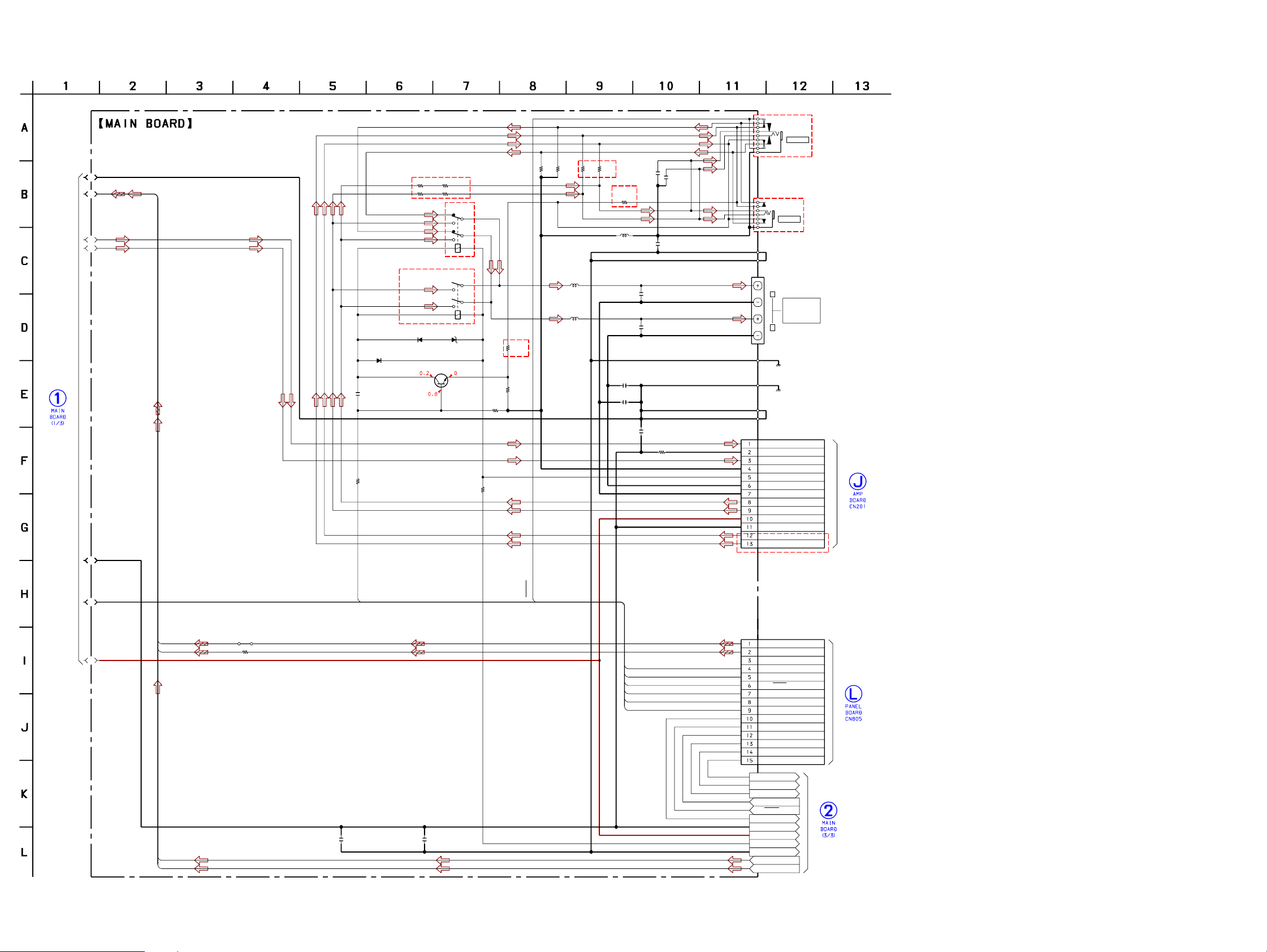
CX-J3000/J3000M
7-14. SCHEMATIC DIAGRAM – MAIN SECTION (2/3) –
(2/3)
∗
R263,264,275,276
180 1/2W
(J3000M:RU)
220 1/2W
(J3000M:E51,MX)
(Page 31)
A1
A2
A3
A4
A5
0.0047
R242
4.7k
D209
1SS133T-77
C241
(J3000M)
(J3000M)
R264
∗
R263 R275
∗∗
MTZJ-77-13B1SS133T-77
*
JR208
0
(J3000)
100k
(J3000M)
R276
RY201
(J3000)
RY202
D211D210
2SC3052F
RELAY
DRIVE
(J3000)
J202
PHONES
L203
1.7µH
L204
1.7µH
(J3000)
R262R261R250R249
100100
(J3000M)
JR203
0
L251 C243
10µH
C244
0.1
C245
0.1
C250
C251
0.01
0.01
(J3000M)
J203
PHONES
0.1
C239
0.01
C240
0.01
C246
0.1
JR209
CN104
11P
13P (J3000)
0
(J3000M)
EP401
EP203
W404
W403
J201
4P
L
SPEAKER
IMPEDANCE
USE 6Ω
R
(CHASSIS)
(CHASSIS)
W401
W402
L-IN
S-GND
R-IN
HP-GND
UNREG
RL-
R1+
L1+
SW_7V
A-GND
R2+
L2+
(J3000)
(Page 35)
R249,250
∗
(J3000M)
0
(J3000)
2.2k
∗
-1
-2
-1
-2
)
JR207
0
(J3000M
Q210
1-LF
JR208
*
R260
10k
R271
470
∗∗
N
-O
P
A6
CD-L
CD-R
A7
TU-L
TU-R
JW601
JR602
0
S
C336C337
0.10.1
N
-O
P
H
CN105
15P
CD-L
CD-R
TU-CE
TU-CLK
TU-DI
TU-DO
ST-IND
TU-ON
A-GND
7V
UNREG
S-GND
TUNER-L
TUNER-R
A-GND
PB2
O-BIAS
HP-ON
SP-ON
F-DATA
F-CLK
TU-ON
ST-IND
TU-DO
TU-DI
TU-CLK
TU-CE
(Page 29)
(Page 33)
PB2
O-BIAS
~~~~~~~~~
HP-ON
SP-ON
F-DATA
F-CLK
CX-J3000/J3000M
3232
Page 33
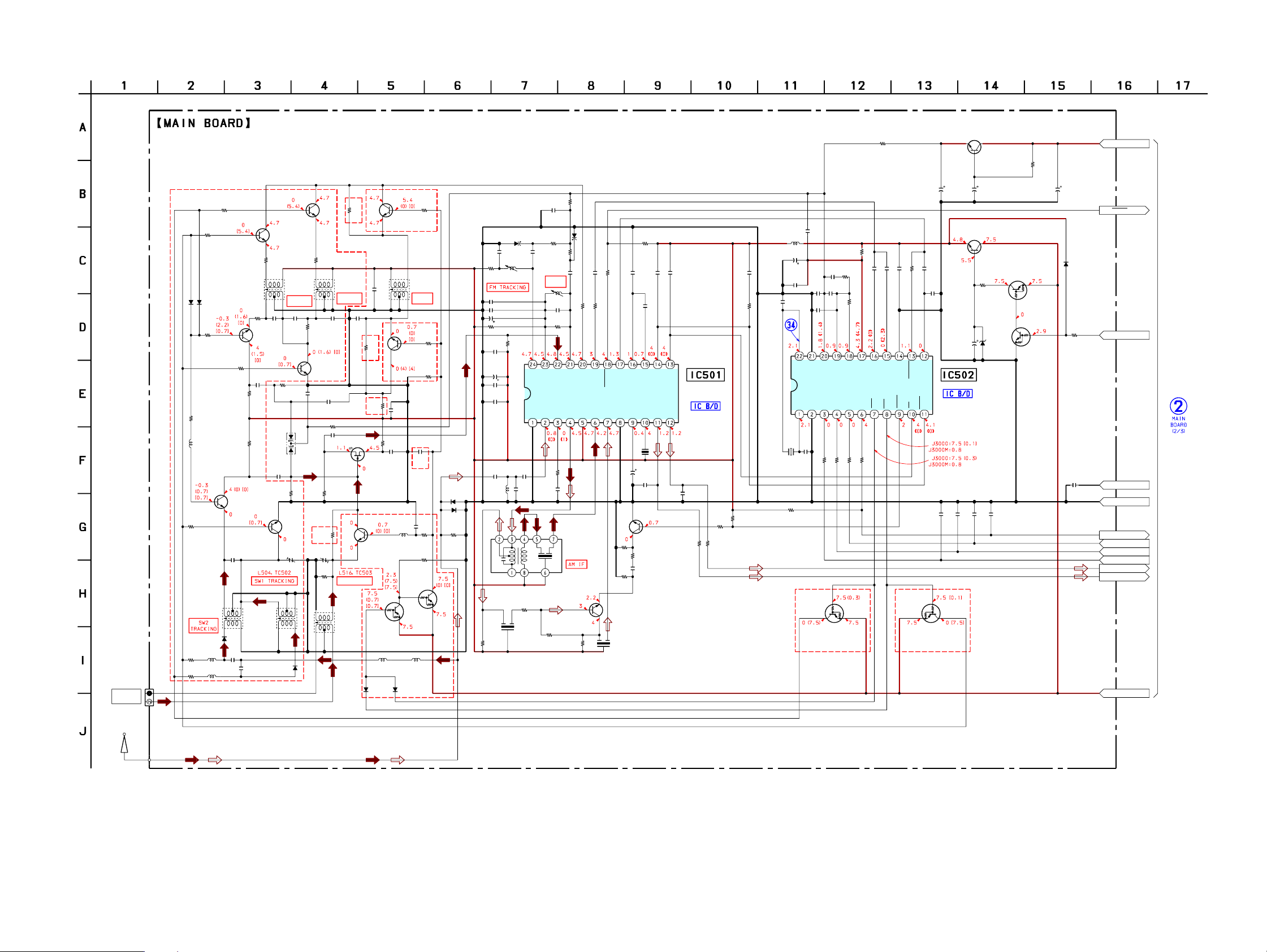
7-15. SCHEMATIC DIAGRAM – MAIN SECTION (3/3) – • See page 27 for Waveforms. • See page 38 for IC Block Diagrams.
(3/3)
CX-J3000/J3000M
ANTTENA
ANT501
FM/SW
TELESCOPIC
ANTENNA
R569
4.7k
C570 C569
47
NC
MUTE
0.1
C561
IF-MUT
BAND SELECT
25V
2.2k
R528
C560
470p
IF-IN
ONO
AM
BEAT
M
Q516Q515
DTA114EKADTA114EKA
SWITCH
(J3000)(J3000)
1000p
C559
PLL
IC502
LC72131D
C564 C565 C566 C567
100p 100p 100p 100p
(J3000)
Q502
R501
4.7k
Q501
2SC5585H
SW2 OSC
1SS133T-77
1SS133T-77
D501
D502
R506
R507 C501
10k 4p
Q504
2SC5585H
OSC SWITCH
R508
C506
1000p
4.7k
R509
2.2M
R519
10k
R514L506
2.2M1mH
Q507
2SC5585H
SW SWITCH
R520
10k
L505
SW2
ANTENNA
D505
1SS133T-77
L507R524
1mH
4.7k
L508R525
1mH4.7k
CN502
LOOP
2P
Q508
2SC5585H
SW SWITCH
C514
12p
ANTENNA
C519
C518 L511 L510
0.01
0.01
2SC5585H
SW1 OSC
R504 R505
10 100
SW2 OSC
VOLTAGE
0
C512
0.01
R521
2.2M
TC502
L504
SW1
D506
1SS133T
-77
L502
SW2 VT
SVC384
D507
2SC5585H
C507R512
R518
2.2k
)
(J3000M
SWITCH
1100k
JR503
TC503
C503R510C502
22p3.3k0.0047
Q505
OSC
C509
560p
2SK302-GR
0
R591
220k
)
0
JR501
(J3000M
L501
SW1 OSC
SW1 VT
VOLTAGE
C505
0
JR502
(J3000M)
R513
2.2M
(J3000)
470
R515
0.01
C513
Q510 C545
TE85L
RF AMP
Q509
2SC5585H
MW SWITCH
MW TRACKING
L516
DTA114EKA
MW ANT
BAND SELECT SWITCH
1SS133T
C504
0.01
22p
Q511
1µH1µH
-77
2SC5585H
MW OSC
R516
470
0.01
Q511,512
Q503
(J3000)
2SC5585H
OSC SWITCH
C517
0.01
L509
1mH
DTA114EKA
D504D503
1SS133T
-77
(J3000)
Q506
(J3000)
L503
MW OSC
MW VT
VOLTAGE
(J3000)
C516
0.01
Q512
R503R502
4.7k10k
D510 R559
HV202A3TRF 47k
C525
0.01
R557
10
L512
FM RF
C527
0.01
C530
0.01
C528
47 10V
R558
R511
10k
R517
22k
D509
1SS133T
-77
D508
1SS133T
R522
-77
10k
R554
2.2k
R552
4.7k
47
C523
R556
0.01
4.7k
C524
47
10V
C540
0.1
C548C511
0.10.1
C520
C522
22p
22p
C521
L517
22p
R529
1.5k
CF501
R527 R531
330 330
R560
1k
D511
C532
0.01
HV202A3TRF
R566
10k
R561C529
4.7k470p
L513
330p
FM OSC
FM VT
VOLTAGE
C533
C531
2p
R562
2.2k
AM
VCC2
RF-IN
FM
RF-OUT
GND2
FM-OSC
IX-O
FM
LO-CUT
RF-IN
M
15k
R526
C539
0.022
L514
AM IF
Q514
2SC27140
BUFFER
R530
47k
AM-OSC
VCC1
100
ST.IND
IF-IN
CF502
R565
IF-REQ
D1
GN
R534
2.2k
R532
330p
C535
DET-O
AGC
CF503
50V
4.7
C544 C543
C541
2SC27140
SWITCHING
R533
0
C542
0.01
1k
1000p
C534
0
0
R564
R563
OSC-O
FM
AM
IF-IN
0.1
0.1
C547
C536
0.22
C537
LPF1
LPF2
PX-IN
M
AD
QU
R-OUT
∗∗
Q513
L-OUT
FM/AM
FRONT END,
IF AMP,EQ
IC501
TA2149N
R536 R535
1k 1k
C538
R523
3.3k
R538R537
10k4.7k
1
0.01
0.015
∗
C543,544
(J3000/J3000M:RU)
(J3000M:E51,MX)
L515
10µH
C555
47 10V
C556
0.01
C549
12p
X501 C550
4.5MHz 15p
R547
100k
X-OUT
X-IN
C593
0.01
C552 C553
0.01 0.01
C592
0.01
GND
X-GND
BAND SELECT
C554 R540
1 4.7k
LP-OUT
CE
4.7k
R548
SWITCH
R542
220
1000p
1000p
C558
C557
3.3k
R541
-IN
-IN
VDD
LP-IN
DI
FM
P-DET
CL
4.7k
R549
AM
1
SW
DO
SW2
4.7k
4.7k
R551
R550
Q520
2SC3052F
1-LF
B+ SWITCH
10
50V
Q517
KTC3198GR-
+5V REGULATOR
R543
2.2k
Q518,519
TUNER ON
SWITCH
C563
10
D512
50V
5.6B
MTZJ-T-77-
Q518
DTA114EKA
DTC114YKA
R567
220k
C568
47
25V
D514
1SS133T-77
R544
1k
Q519
-T146
C571
0.1
UNREG
ST-IND
TU-ON
S-GND
A-GND
TU-DO
TU-CLK
TU-DI
TU-CE
TUNER-L
TUNER-R
(Page 32)
7V
CX-J3000/J3000M
CN501
1P
3333
Page 34
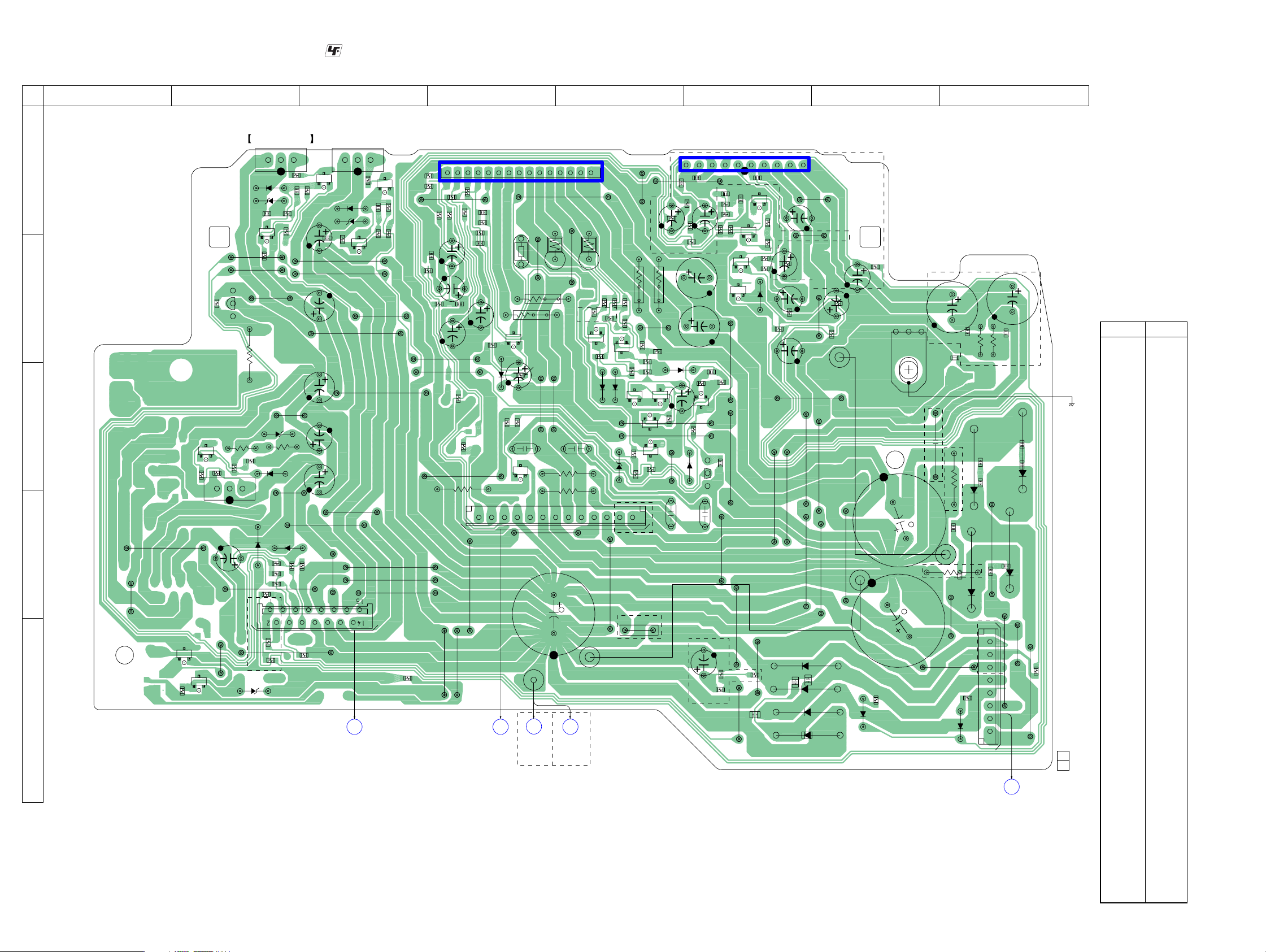
CX-J3000/J3000M
7-16. PRINTED WIRING BOARD – AMP SECTION – • : Uses unleaded solder. • See page 21 for Circuit Boards Location.
1 2 3 4 5 6 7 8
D
A
B
C
E
JW156
JW139
Q158
E
R170
EB
Q155
E
Q160
E
R173
R163
R169
Q154
Q157
C108
JW162
JW161
E
R166
R171
C
(J3000)
JW150
AMP BOARD
Q152
JW126
Q101
E
R101
D101
D102
Q103
C102
R104
JW160
JW159
C163
JW157
C169
JW137
JW125
Q151
EBCEB
C162
Q153
R164
R112
R109
R161
JW168
D164
R122
R106
E
D163
R107
R158
R167
R160
JW138
JW146
D176
R110
R162
R157
C161
R113
R159
C103
C159
C168
R111
CN102
JW149
D160
D161
R168
D170
JW144
D173
H
PANEL
BOARD
CN804
(Page 28)
(J3000)
C
E
JW158
JW153
C101
R105
Q102
IC202
E
R103
R102
JW123
JW122
JW166
R174
R256
R255
C225
C203
R201
R253
R202
R269
C207
15
R236
R238
C160
CN206
F
CD
BOARD
(J3000)
R220
R219
JW143
JW113
JW152
CN201
JW121
R204
JW141
(Page 25)
R235
JW133
C217
R254
R270
C226
JW155
JW154
JW163
C204
R226
JW164
R257
R258
C218
C208
R225
JW128
R273
113
JW167
R237
D206
R241
TH202
Q254
C211
E
C258
Q209
E
J
MAIN
BOARD
(Page 22)
CN104
(Page 30)
JW151
(J3000M: E51, MX)
C257
R267
R268
G
CD/MP3
BOARD
(J3000M)
R244
E
W101
R203
Q202
1
R206
R210
D202
R243
R218
E
D201
D203
R217
Q201
(J3000)
JW107
(J3000M)
R205
R212
R209
Q205
Q207
R231
R222
JW001
JW148
R259
R208
E
E
E
JW140
Q206
R221
R213
R207
JW145
Q204
R240
C214
E
JW135
JW134
C228
10
R233
D204
C219
R216
R215
C229
JW132
R214
R239
C238
C209
C213
R211
E
Q203
R280
Q208
D205
C227
(J3000)
C104
C230
C249
G
D
S
R272
R156
R154
C224
R228
R227
C237
JW114
C223
R230
R229
Q253
Q104
JW136
JW131
JW105
R155
JW106
Q251
E
IC201
D106
R252
R251
C212
R279
C210
1
R232
JW112
C215
JW129
JW130
C107
R117
W103
C216
R119
R234
EP201
C233
JR204
C235
R246
C234
R245
(J3000)
C236
• Semiconductor
Location
Ref. No. Location
D101 A-3
D102 A-3
C220
Q252
E
E
R278
E
R277
R120
C106
D104 E-8
D105 E-7
JW127
(J3000M)
(CHASSIS)
D106 B-6
D151 E-6
D152 E-6
D153 E-6
D154 E-6
D155 D-8
D156 C-8
D157 D-8
D158 C-8
D160 A-2
D161 A-2
D163 C-2
D164 C-2
D170 D-2
D173 E-2
D176 D-2
D201 C-5
D202 C-5
D203 C-5
D204 C-5
D205 C-6
D206 C-4
IC201 A-6
IC202 A-4
Q101 A-3
Q102 A-3
Q103 B-3
Q104 B-6
Q151 A-2
Q152 A-3
Q153 A-2
Q154 B-2
Q155 E-2
Q157 C-2
Q158 C-2
Q160 E-2
Q201 B-5
Q202 B-5
Q203 C-6
C154
JW104
JW110
JW109
C151
JW124
JW119
D153
C152
JW120
D151
D154
D152
JW118
C153
JW108
W102
D105
C201
C202
R116
(J3000)
JW115
R247
(J3000)
W104
D104
R248
C171
C170
JW111
JW116
R115
D158
C156
D157
(J3000)
CN202
8
1
C173
C172
JW117
C155
K
C158
C157
D155
JW103
1-862-946-
PT BOARD
(Page 36)
D156
JW169
R118
JW101
11
(11)
CN005
Q204 C-5
Q205 C-5
Q206 C-5
Q207 C-5
Q208 C-6
Q209 C-4
Q251 A-6
Q252 A-6
Q253 B-6
Q254 B-4
CX-J3000/J3000M
3434
Page 35
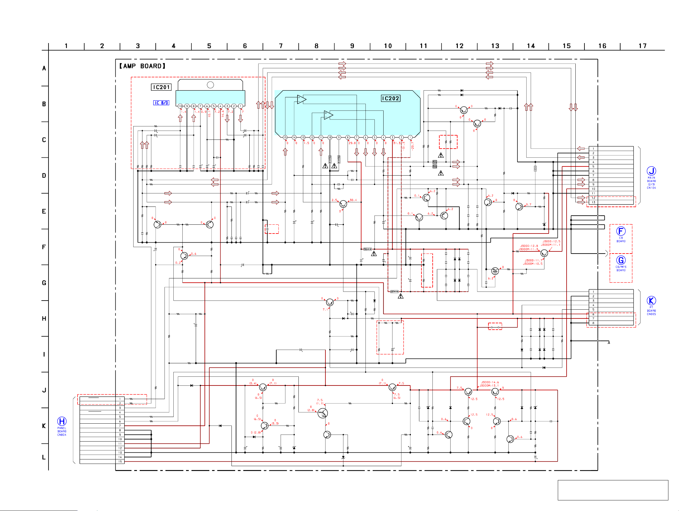
7-17. SCHEMATIC DIAGRAM – AMP SECTION – • See page 38 for IC Block Diagrams.
CX-J3000/J3000M
(J3000)
GND
POWER ON
R120
47k
C217
R257
C211
10
50V
Q104
2SA1235
MUTING
1SS133T-77
10p
47k
F
IC202
(J3000/J3000M:RU)
(J3000M:E51,MX)
SUB
+PRE
R258
C218
Q254
2SC3052F
1-LF
STANDBY
SWITCH
R119
2.2k
C107
D106
R117
C106
47k
10p
47
10V
22k
1
50V
T-CH2
T-CH1
OU
OUT-CH2
OU
R217
47k
C219
R213
100
100k
10V
R259
100
C209 C238
∗∗
D206
1SS133T-77
R237 R236
33k 10k
R118
2.2k
R156
3.3k
POWER AMP
OUT-CH1
1SS133T-7715k
D202R210
1k
R244
D201
:E51,MX)
(J3000M
C257
0.33
C227
0.33
R267 R268
2.2
1/2W
D157
1N5401M
D158
1N5401M
1SS133T-77
C258
0.33
C228
0.33
2.2
1/2W
C171
0.1
C172
0.1
C173
0.1
D204R207
C249
1SS133T-7710k
0.1
R208
10k
Q202
2SA1235
F
Q201,202
OVER LOAD
DETECT
D205
R273
47 1/2W (J3000M)
68 1/2W (J3000)
R115
1k
D104
R241
4.7k
2SC3052F
THERMAL
DETECT
TH202
R221
10k
Q206
1-LF
D203
MTZJ-77-5.1B
0.1
C151
0.1
C152
R222
1k
R231
10k
D151
2A02M
D152
2A02M
1SS133T-77
Q209
2SA1235
B+ SWITCH
0.1
C153
D153
2A02M
R116
1k
0.1
C154
D154
2A02M
D105
R272
47k
1SS133T-77
Q203
2SC3052F
1-LF
R211
470k
PROTECT
DETECT
R280
10k
R238
4.7k
S
Q208
2SK2541-T
PROTECT
C237
SWITCH
0.1
JW001
(J3000M)
1SS133T-77
CN201
(J3000M)
11P
13P (J3000)
CN202
(J3000M)
(J3000)5P8P
CN206
EP201
L-IN
S-GND
R-IN
HP-GND
UNREG
R-
L-
R1+
L1+
SW_7V
A-GND
R2+
L2+
W104
W103
W102
W101
(J3000)
(Page 32)
(Page 23)
1P
(J3000)
(Page 26)
(J3000M)
AC1
AC-GND
AC2
AC3
AC4
(CHASSIS)
AC/DC
AC-OP
BATT-GND
(J3000)
(Page 37)
15k
R209
Q201
2SA1235
F
+VCC
-VCC
-PRE
R218
47k
R212
100k
Q204
2SC3052F
1-LF
Q205
2SC3052F
1-LF
Q204,205,207
DC DETECT
C201
R247
∗
2.2k
1/2W
R248
C202
2.2k
∗
1/2W
∗
C201,202
(J3000M:RU)
(EXCEPT J3000M:RU)
(J3000)
R233
100
2200 35V
2200 50V
R155R154
2.2k10k
C104
22
50V
(J3000)
1k
R205R206
R243
1k1k
R203
0.22
2W
R204
0.22
2W
R216
22k
Q207
2SA1235
C155 C170
0.1 0.1
D155
C156
0.1
C157
0.1
D156
C158
0.1
1N5401M
1N5401M
STK433-030
C207C208
22
50V
C209,238
NF-CH1
(J3000)
(J3000M)
STK433-060
IN-CH1
R219 R220
11
POWER AMP
IC201
LA4600
R234
C213
C214
47k
47k
2.7k
2.7k
R239
R240
R214
R215
R225
18k
R226
18k
0
R227
100p
10k
Q251 R252R251
2SC3052F
C223
R229
1-LF
C210
10
50V
4.7k
1 50V
1 50V
IN-1
S-GND
STBY
IN-2
P-P
FILTER
10V
16V
2SA1235
MUTING
47
25V
50V
0.001
100
4.7
100
C230
Q253
F
C216
Q252
2SC3052F
1-LF
R111
4.7k
C215
C212
R278
47k
R277R279
1M22k
0.001
C229
Q251,252
MUTING
2.2k2.2k
CONTROL
R122
4.7k
C108
R112
3.9k
(J3000)
5.6k
(J3000M)
R113
2.2k
P-GND
VCC
C220
0.001
OUT-1
OUT-2
C233
1000
16V
ST-BY
NF-CH2
C234
1000
R232
470k
16V
220
220
0.001
0.001
R245
R246
C235
C236
C225
220p
C204
C160
2200
4.7 50V
25V
R269
1k
R270
C226
4.7
1k
50V
JR204
R201
10k
R202
10k
0
R228
220p
100p
10k
C203
C224
R230
IN-CH2
R256 R255
R254 R253
47k 47k
∗∗
22
)
0.01
50V
(J3000M
∗
1.2k
(J3000M:E51,MX)
1.5k (J3000/J3000M:RU)
JW115
0
R253,254
R235
4.7k
∗
100 35V
100 50V
C159
220
16V
(Page 29)
CX-J3000/J3000M
(J3000)
OP-BATT
AMP-ON
O-MUTE
I-PROTECT
POWER-ON
CD-ON
UNREG
VP-GND
CD-D-GND
A-GND
P-VDD(7V)
D-VDD(3.3V)
CD-P-GND
MT-GND
SW_9V
13P
(J3000M)
15P (J3000)
CN102
Q157
R107
100
R109
1k
R106
1k
R110
100
R162
1k
D176
1SS133T
-77
D170
1SS133T-77
C169
470
10V
2SB1375
R170 R167
100 100
+3.3V REGULATOR
2SC3052F
T1-LF
D164
1SS133T-77
R171
470
Q158
R169
47k
Q157,158
Q154
2SA1296GR
R166
470
Q155
DTC114YKA-T146
R168
CD/VCD ON
100
SWITCH
Q160
2SC3052F
T1-LF
LOW BATTERY
C168
100
10V
D163
MTZJ-T-77-3.3A
DETECT
R164
470
R173
470k
D173
MTZJ-77-3.3A
B+ SWITCH
R163
47k
C162
0.1
D161
MTZJ-77-5.1B
R160 C161
1.5k 0.001
R174
1k
C163
220
16V
Q153
2SC3052F
T1-LF
R161
470
+7V REGULATOR +9V REGULATOR
Q151 Q101
2SB1375 2SB1375
D160R159
1SS133T-774.7k
Q152
2SC3052F
T1-LF
Q151-153
R157 R101
100 100
Q102
2SC3052F
T1-LF
R158 R102
68 68
D101 R103
1SS133T-77 4.7k
Q103
2SC3052F
T1-LF
Q101-103
MTZJ-77-6.8B
R104C101
1.5k0.001
R105
470
C103
100
16V
D102
C102
0.1
The components identified by mark 0 or dotted
line with mark 0 are critical for safety.
3535
Replace only with part number specified.
Page 36
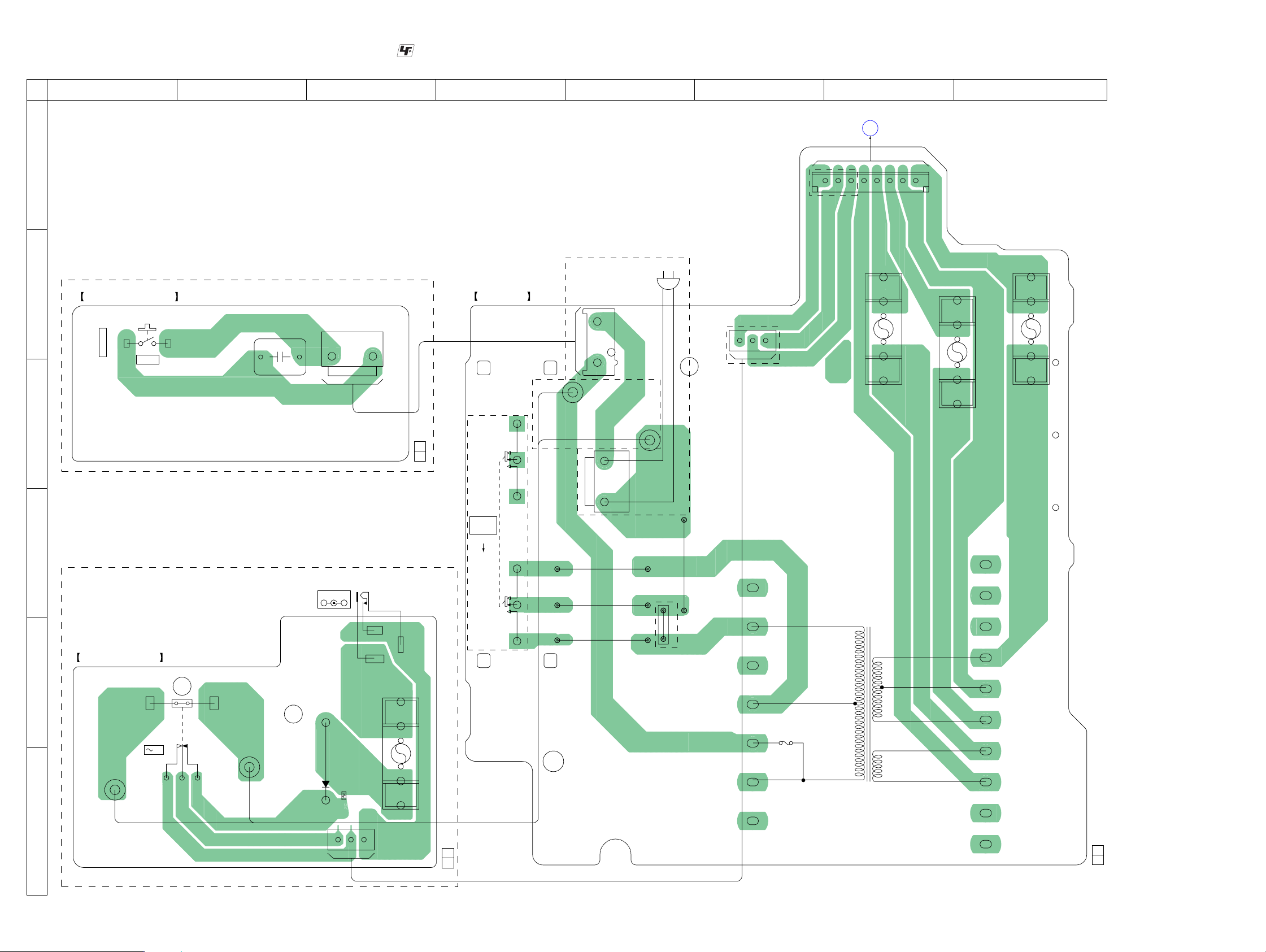
CX-J3000/J3000M
7-18. PRINTED WIRING BOARDS – POWER SUPPLY SECTION – • : Uses unleaded solder. • See page 21 for Circuit Boards Location.
1 2 3 4 5 6 7 8
K
AMP BOARD
CN202
(Page 34)
A
B
C
(J3000M)
POWER-SW BOARD
S001
POWER
C001
CN003
21
1-862-944-11(11)
PT BOARD
(J3000M: E51)
8
(J3000)
(J3000M)
CN006
2
1
RED2
W003
RED1
1
-2
CN004
(J3000)
W001
(AC IN)
(J3000)
3
1
W005
CN005
F003
1
F001
F002
D
2
JW013
JW012
JW011
JW002
(J3000/J3000M: RU, MX)
JW014
8
7
PT001 (J3000M: E51)
PT002 (J3000/J3000M: RU, MX)
POWER TRANSFORMER
(J3000)
AC INLET BOARD
J001
DC IN 12V
–
S2
VOLATGE
SELECTOR
110 – 120V
220 – 240V
-1
+
E
1
∗
NOT REPLACEABLE:
∗
BUILT IN TRANSFORMER
17
1-862-942-11(11)
J002
AC
W004
F
RED2
W002
RED1
D001
F004
R001
31
W006
1-861-943-11(11)
CX-J3000/J3000M
3636
Page 37
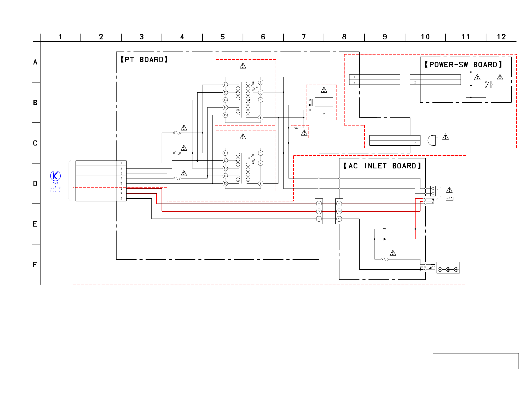
7-19. SCHEMATIC DIAGRAM – POWER SUPPLY SECTION –
CX-J3000/J3000M
(J3000M:E51)
(Page 35)
AC1
AC-GND
AC2
AC3
AC4
AC/DC
AC-OP
BATT-GND
CN005
5P
(J3000M)
8P (J3000)
T4AL 250V
T5AL 250V
∗
F001,002
(J3000/J3000M:RU)
(J3000M:E51,MX)
F001
F002
F003
T2AL
250V
W002
W004
W006
CN006
2P
LOAD
LIVE
LIVE
NEUTRAL
CN004
2P
CN003
2P
LOAD
LIVE
(AC IN)
J002
(J3000)
C001
2200p
250V
S001
POWER
(J3000M)
PT001
POWER TRANSFORMER
(J3000M:E51)
0V
115V
230V
∗
∗
(J3000/J3000M:RU,MX)
POWER TRANSFORMER
∗
NOT REPLACEABLE:
BUILT IN TRANSFORMER
PT002
0V
230V
JW002
0
(J3000/J3000M:RU,MX)
W005
S2
VOLTAGE
SELECTOR
110-120V
220-240V
W001
W003
3P 3P
R001
10k
D001
RK46LF-T2
F004
T5AL
250V
J001
DC IN 12V
The components identified by mark 0 or dotted
line with mark 0 are critical for safety.
Replace only with part number specified.
CX-J3000/J3000M
3737
Page 38
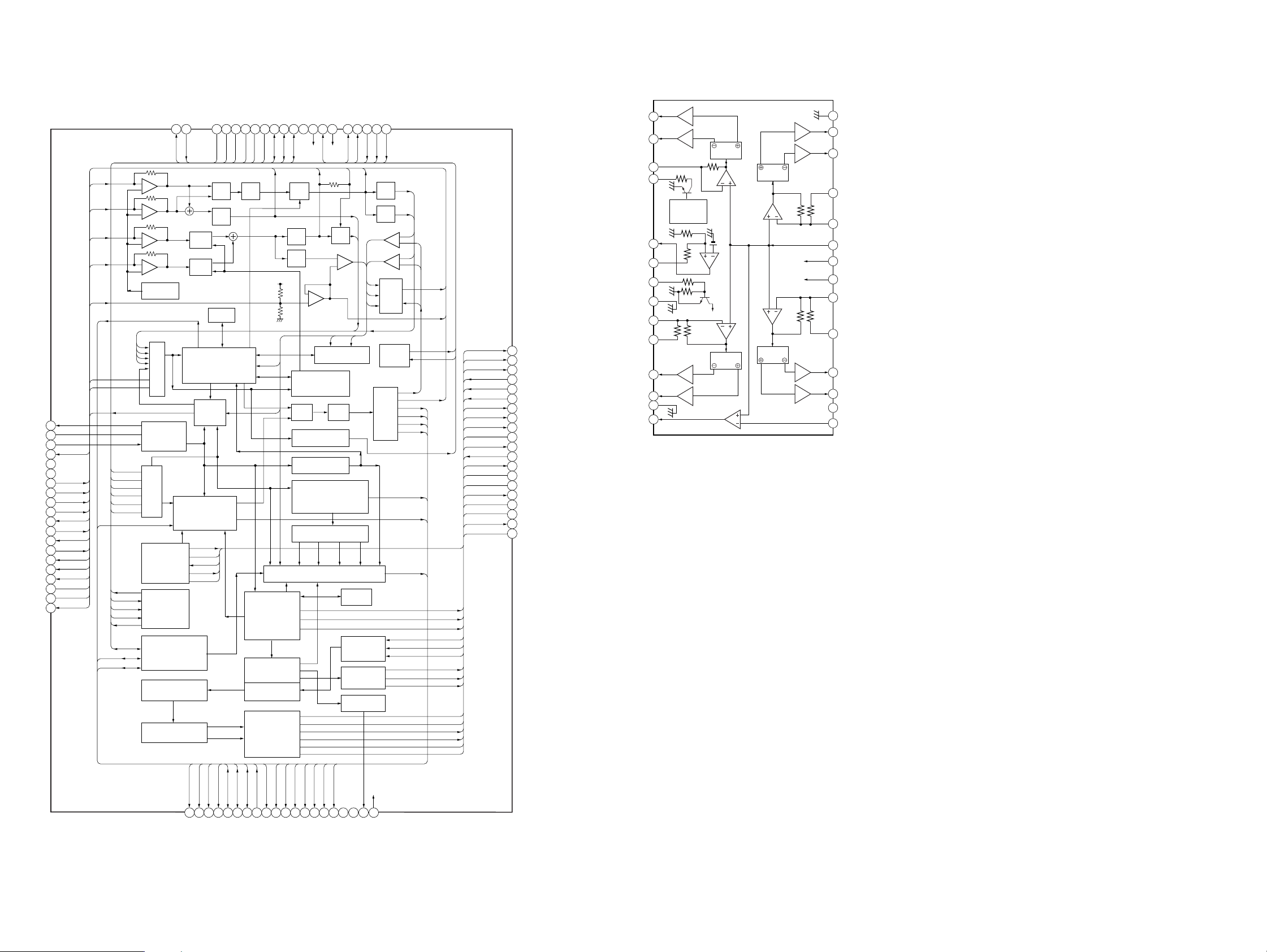
CX-J3000/J3000M
• IC Block Diagrams
– CD Board –
IC701 LC78646E-E
FIN1
FIN2
TIN1
TIN2
REFI
DEFECT
ADAVDD
ADAVSS
JITTC
SLCO
1
SLCO
SLCIST
EFMIN
RFVDD
RFVSS
VREF
RFMON
JITTC
ADAVDD
ADAVSS
FIN1
FIN2
TIN1
TIN2
REFI
TEC
TDO
SLCIST
2
EFMIN
3
RF
4
RF
5
6
FIN1
7
FIN2
8
TIN1
9
TIN2
10
VREF
11
REFI
12
FE
13
FE
TE
14
15
16
17
18
19
20
TEC
TE
RFMON
JITTC
ADAVDD
ADAVSS
TDO
PDO1
PDO2
FR
PCKIST
VVDD
VVSS
SBCK/FG
WRQ
CL
CE
DI
DO
CONT1-3
SBCK/CONT6
CONT4,5
LDS80LDD
79 78 77 76 75 74 73 72 71
LDS
LDD
+
–
+
–
+
–
+
–
LEVEL SET
A/D
SLICE LEVEL
CONTROL
PLL
VCEC
CLOCK
GENERATOR
COMMAND
INTERFACE
GENERAL PURPOSE
DIGITAL FILTER
SERVO PROCESSOR
CONTROL
PORTS
8FS
1BIT DAC
TBAL
TBAL
JITTER
DETECT
CLV,CAV
16MOUT
XVSS
XIN
XOUT
XVDD
FR
MIX
LPF
RAM
FR
VVDD
VVDD
PCKIST
VVSS
PCKIST
VVSS
EQ
INTERPOLATION
PDO2
PDO1
CONT1
CONT270CONT3
PDO2
PDO1
CONT1
CONT2
CONT3
FE
AGC
LPF
LPF
AUTO ADJUST
SW
RUPTURE DEFECT
DETECT,PROTECT,INSERT,
SUBCODE DECODE CRC
MONITOR SIGNAL SELECTOR
ERROR
CORRECTION
AUDIO CD
MUTE
ATTENUATION
DEEMPHASIS
LPF
VSS
VDD5
DRF
RES
DRF
TE
SW
TRACK JUMP
D/A
WRQDODICLCE
WRQDODICLCE
RF
TEC
+
–
RAM
EXTERNAL
AUDIO IN
SERIAL
OUT
AUDIO OUT
S/H
69 68 67 66 65 64 63 62 61
–
+
DRF
FRAME SYNC
EFM DECODE
PH
BH
MONI
CONT
APC
+
–
+
–
FDO
SPDO
SLDO
GPDAC
FSEQ
MONI1-5
V/P
RFMON
VREF
LDD
LDS
TDO
FSX/16MIN
ASDACK
ASLRCK
DATACK
DRF
EFLG
ASDFIN
DATA
LRSY
LVDD
LVSS
LCHO
RCHO
RVDD
RVSS
C2F
DATA
DATACK
LRSY
ASDFIN
ASDACK
ASLRCK
16MOUT
EFLG
C2F
XVSS
FSX/16MIN
XIN
XOUT
XVDD
RVDD
RCHO
RVSS
LVSS
LCHO
LVDD
60
59
58
57
56
55
54
53
52
51
50
49
48
47
46
45
44
43
42
41
DATA
DATACK
LRSY
ASDFIN
ASDACK
ASLRCK
16MOUT
EFLG
C2F
XVSS
FSX/16MIN
XIN
XOUT
XVDD
RVDD
RCHO
RVSS
LVSS
LCHO
LVDD
IC702 BA5826FP-E2
1
SP–
D.BUFF
2
SP+
D.BUFF
3
SPIN
4
RST
THERMAL
SHUT-DOWN
MONITOR
5
REG–B
6
REGO
MUTE
7
GND
TIN
(TIN)
GND
OPOUT
8
9
10
T–
11
T+
12
13
14
D.BUFF
D.BUFF
DRIVER
MUTE
LEVEL
SHIFT
REGULATOR
LEVEL
SHIFT
LEVEL
SHIFT
LEVEL
SHIFT
D.BUFF
D.BUFF
VCC
VCC
D.BUFF
D.BUFF
28
GND
27
SL–
SL+
26
25
SLIN
24
(SLIN)
23
VREF
VCC
22
VCC
21
20
(FIN)
FIN
19
F–
18
F+
17
NC
16
OPIN
15
CX-J3000/J3000M
SBCK/FG
SBCK/CONT6
CONT5
SBCK/FG
SBCK/CONT6
V/P
DEFECT
DEFECT
V/P
FSEQ
FSEQ
MONI1
MONI2
MONI1
MONI3
MONI2
MONI3
MONI4
MONI5
MONI4
MONI5
VSS
FDO
SLDO
SPDO
CONT4
CONT5
GPDAC
21 22 23 24 25 26 27 28 29 30 31 32 33 34 35 36 37 38
FDO
SLDO
SPDO
CONT4
GPDAC
39 40
DOUT
VDD(3.3V)
TEST
3838
Page 39

– CD/MP3 Board –
IC701 LC78646E-E
FIN1
FIN2
TIN1
TIN2
REFI
DEFECT
+
–
+
–
+
–
+
–
LEVEL SET
LDS80LDD
FR
VVDD
PCKIST
VVSS
VVDD
PCKIST
VVSS
PDO2
PDO2
EQ
79 78 77 76 75 74 73 72 71
LDS
LDD
FR
MIX
LPF
TBAL
TBAL
RAM
PDO1
PDO1
VSS
VDD5
CONT1
CONT1
CONT2
FE
CONT270CONT3
CONT3
LPF
LPF
DRF
69 68 67 66 65 64 63 62 61
DRF
TE
AGC
–
+
RES
WRQDODICLCE
WRQDODICLCE
TEC
SW
+
–
CX-J3000/J3000M
RF
PH
BH
+
–
+
–
MONI
CONT
RFMON
VREF
SLCO
SLCIST
EFMIN
RFVDD
RFVSS
FIN1
FIN2
TIN1
TIN2
VREF
REFI
TEC
RFMON
JITTC
ADAVDD
ADAVSS
TDO
DRF
ASDFIN
DATA
LRSY
LVDD
LVSS
LCHO
RCHO
RVDD
RVSS
EFLG
C2F
DATA
DATACK
LRSY
ASDFIN
ASDACK
ASLRCK
16MOUT
EFLG
C2F
XVSS
FSX/16MIN
XIN
XOUT
XVDD
RVDD
RCHO
RVSS
LVSS
LCHO
LVDD
60
59
58
57
56
55
54
53
52
51
50
49
48
47
46
45
44
43
42
41
DATA
DATACK
LRSY
ASDFIN
ASDACK
ASLRCK
16MOUT
EFLG
C2F
XVSS
FSX/16MIN
XIN
XOUT
XVDD
RVDD
RCHO
RVSS
LVSS
LCHO
LVDD
FDO
SPDO
SLDO
GPDAC
FSEQ
V/P
LDD
LDS
TDO
FSX/16MIN
ASDACK
ASLRCK
DATACK
TRACK JUMP
AUTO ADJUST
SW
RUPTURE DEFECT
DETECT,PROTECT,INSERT,
SUBCODE DECODE CRC
D/A
DRF
FRAME SYNC
EFM DECODE
RAM
EXTERNAL
AUDIO IN
SERIAL
AUDIO OUT
PORTS
8FS
1BIT DAC
SERVO PROCESSOR
JITTER
DETECT
CLV,CAV
CONTROL
16MOUT
XVSS
XIN
XOUT
XVDD
MONITOR SIGNAL SELECTOR
ERROR
CORRECTION
AUDIO CD
INTERPOLATION
MUTE
ATTENUATION
DEEMPHASIS
LPF
ADAVDD
ADAVSS
JITTC
SLCO
1
SLCIST
2
EFMIN
3
RF
4
RF
5
6
FIN1
7
FIN2
8
TIN1
9
TIN2
10
VREF
11
REFI
12
FE
13
FE
TE
14
15
16
17
18
19
20
TEC
TE
RFMON
JITTC
ADAVDD
ADAVSS
TDO
PDO1
PDO2
FR
PCKIST
VVDD
VVSS
SBCK/FG
WRQ
CL
CE
DI
DO
CONT1-3
SBCK/CONT6
CONT4,5
A/D
SLICE LEVEL
CONTROL
PLL
VCEC
CLOCK
GENERATOR
COMMAND
INTERFACE
GENERAL PURPOSE
DIGITAL FILTER
APC
S/H
MONI1-5
OUT
FDO
SLDO
SPDO
CONT4
CONT5
GPDAC
21 22 23 24 25 26 27 28 29 30 31 32 33 34 35 36 37 38
FDO
SLDO
SPDO
CONT4
CONT5
GPDAC
DEFECT
SBCK/FG
SBCK/CONT6
DEFECT
SBCK/FG
SBCK/CONT6
V/P
V/P
FSEQ
FSEQ
MONI1
MONI2
MONI1
MONI3
MONI2
MONI3
MONI4
MONI4
MONI5
MONI5
VSS
39 40
DOUT
VDD(3.3V)
TEST
39
Page 40
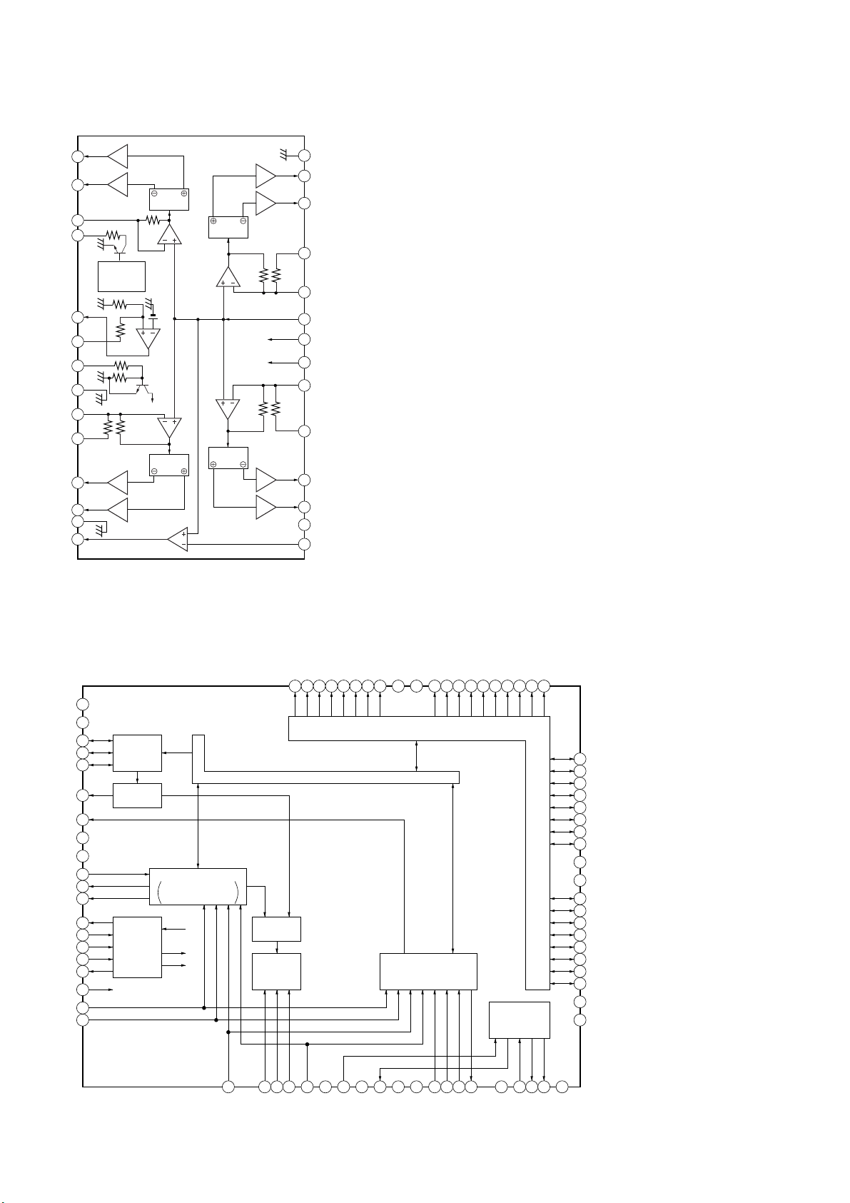
CX-J3000/J3000M
IC702 BA5826FP-E2
1
SP–
D.BUFF
2
SP+
SPIN
RST
REG–B
REGO
MUTE
GND
TIN
(TIN)
GND
OPOUT
D.BUFF
3
4
THERMAL
SHUT-DOWN
MONITOR
5
6
7
8
9
10
D.BUFF
T–
11
D.BUFF
T+
12
13
14
DRIVER
MUTE
LEVEL
SHIFT
REGULATOR
LEVEL
SHIFT
LEVEL
SHIFT
LEVEL
SHIFT
VCC
VCC
D.BUFF
D.BUFF
D.BUFF
D.BUFF
28
GND
27
SL–
SL+
26
25
SLIN
24
(SLIN)
23
VREF
VCC
22
VCC
21
20
(FIN)
FIN
19
F–
18
F+
17
NC
16
OPIN
15
IC1001 LC78684E-E
DVDD5
61
62
VSS
STREQ
STCK 64
STDAT 65
FSYNC 66
CRCF 67
DVDD6
VSS
WOK 70
CNTOK 71
OVF 72
CMDOUT 73
CMDIN 74
CL 75
CE 76
INTB 77
RESB 78
DATAIN 79
DATACK
63
68
69
80
DATA
INTERFACE
MP3
DECODER
CPU
INTERFACE
ANTI-SHOCK
COMPRESSION/
NON-COMPRESSION
MUX
AUDIO
INTERFACE
MADRS0
59
60
MADRS2
MADRS1
57
58
DATA BUS
MADRS4
MADRS3
55
56
MADRS6
MADRS5
53
54
VSS
MADRS7
52
INTERFACE
DVDD4
51
D-RAM
CD-ROM
DECODER
MADRS8
50
MADRS9
48
49
MADRS11
MADRS10
46
47
CASUB
OEB45MADRS12
43
44
SYSTEM
CLOCK
GENERATOR
WEB42CASLB
41
RASB
32
31
23
22
MDATA1540
MDATA1439
MDATA1338
MDATA1237
MDATA1136
MDATA1035
MDATA934
MDATA833
VSS
DVDD3
MDATA730
MDATA629
MDATA528
MDATA427
MDATA326
MDATA225
MDATA124
MDATA0
VSS
DVDD221
40
1
LRSY
2
ADDATA
3
ADBCK
4
ADLRCK
5
C2FIN
6
TEST1
7
CKIN
10
11PW12
13
14
15
SFSY
SBCK
16
AVDD
17
18
VCOC
VPRFR
19
VPDO
20
AVSS
8
9
VSS
CKOUT
TEST2
DVDD1
SBSY
Page 41

– MAIN Board –
IC302 BD3881FV
CX-J3000/J3000M
REC1O27REC1N
28
1
2
PB1P3PB2P
PB1N
IC501 TA2149N
REC2N25REC2O24INC223INC122INB221INB120INA219INA1
26
VOLUME
VOLUME
4
PB2N
5
PB2O
6
PB1O
7
VOLIN18VOLIN2
OUT117BAS116OUT215BAS2
18
BASS
TREBLE
9
GND
10
TRE1
TREBLE
11
TRE2
BASS
12
VDD
LOGIC
CONTROL
13
CONT
14
VEE
RF GND
FM RFIN
AM LOW CUT
MIX OUT
VCC
AM IF IN
FM IF IN
GND
AGC
QUAD
R-OUT
L-OUT
24
23
22
21
20
19
18
17
16
15
14
13
FM RFOUT
RF VCC
AM RFIN
FM OSC
AM OSC
OSC OUT
ST LED
IF REQ
DET OUT
MPX IN
LPF1
LPF2
1
FM RF
2
3
4
5
6
7
8
9
10
11
MUTE
12
AM IF
FM IF
AGC
FM
MIX
AM
MIX
LEVEL
DET
AM
DET
FM
DET
ST/MO
FM/AM
FM
OSC
AM
OSC
AF BUFF
VCO
DIVIDE
DECODE
1/1 OR
1/16
IF REQ
BUFF
ST
SW
AF
BUFF
IF BUFF
1/8
41
Page 42

CX-J3000/J3000M
IC502 LC72131D
VSS
AOUT
XOUT
2122
AIN
19
20
REFERENCE
DIVIDER
PHASE
DETECTOR
CHARGE PUMP
UNLOCK
DETECTOR
PD
18
SWALLOW COUNTER
1/16, 1/17 4BITS
12BITS
PROGRAMMABLE
DRIVER
17
POWER
ON
RESET
VDD
NC
AMIN
IO2
FMIN
15
16
1/2
14
IFIN
12
13
CCB
INTERFACE
3
2
5
4
1
NC
XIN
6
DI
CE
CL
– AMP Board –
IC201 LA4600
TSD
PROTECTOR
OUTPUT
AMP
OUTPUT
AMP
DO
PRE
DRIVE AMP
PRE
DRIVE AMP
RIPPLE
FILTER
DATA SHIFT REGISTER LATCH
7
POP NOISE
PREVENTION
CIRCUIT
INPUT
AMP
INPUT
AMP
STANDBY
SWITCH
9
8
BO2
BO1
REFERENCE
BO3
AMP
UNIVERSAL
COUNTER
10
11
IO1
BO4
42
OUT1
GND
OUT2
VCC
FILTER
10987654321
P. P.
STANDBY
IN2
GND
IN1
Page 43

• IC Pin Function Description
PANEL BOARD IC801 (SYSTEM CONTROLLER)
LC877448A-54A6-E (CX-J3000) LC8774725C-54A4-E (CX-J3000M)
Pin No. Pin Name I/O Description
1 O_CD_RST O
2 O_TU_CE O Chip enable signal output to the PLL
3 O_CD_DATA
4 I_CD_DATA I
5 O_CD_CLK
6 O_TU_DATA O Serial data output to the PLL
7 I_TU_DATA I Serial data input from the PLL
8 O_TU_CLK O Serial clock signal output to the PLL
9 I_CD_DRF I DRF signal input from the CD DSP
10 O_AMP_ON2 O Not used
11 RES I
12 I_XT1 I Not used
13 O_XT2 O Not used
14 VSS1 – Ground terminal
15 I_CF1 I Main system clock input terminal (8.64 MHz)
16 O_CF2 O Main system clock output terminal (8.64 MHz)
17 VDD1 – Power supply terminal (+3.3V)
18 I_POWER_DN I Power down monitor input terminal “L”: power down
19 I_PROTECT I Abnormal voltage monitor input terminal (A/D input)
20 I_SUFFIX I Destination setting terminal (A/D input)
21 I_OP_BATT I
22 I_CD_LID I
23 I_VOL_ENC I Jog dial pulse input from the rotary encoder (VOLUME)
24, 25 I_KEY1, I_KEY2 I Front panel key input terminal (A/D input)
26 I_CD_WRQ I WRQ signal input from the CD DSP
27
28 I_CD_FSEQ I FSEQ signal input from the CD DSP
29 I_REM I Remote control signal input from the remote control receiver
30 I_A_MODE I
31 I_A_PHOTO I
32 I_A_HALF I
33 I_REC_FWD I
34 I_B_PHOTO I
I_MP3_INTB/
I-HP INTB signal input from the MP3 decoder (CX-J3000M)
Reset signal output to the CD DSP “L”: reset (CX-J3000)
Reset signal output to the CD DSP and MP3 decoder “L”: reset (CX-J3000M)”
O Serial data output to the CD DSP (CX-J3000)
Serial data output to the CD DSP and MP3 decoder (CX-J3000M)
Serial data input from the CD DSP (CX-J3000)
Serial data input from the CD DSP and MP3 decoder (CX-J3000M)
O Serial clock signal output to the CD DSP (CX-J3000)
Serial clock signal output to the CD DSP and MP3 decoder (CX-J3000M)
Reset signal input terminal “L”: reset
For several hundreds msec. after the power supply rises, “L” is input, then it
changes to “H”
Battery drive detection signal input terminal “L”: DC power, “H”: AC power
(CX-J3000 only)
CD lid open/close detection signal input terminal “L”: CD lid is closed, “H”: CD
lid is opened
Headphone in detection signal input terminal “L”: headphone in (CX-J3000)
I
Deck A mode detect switch input from the tape mechanism deck block
“L”: Deck A mode
Deck A side photo sensor detection signal input from the tape mechanism deck
block
Deck A side cassette in detect switch input from the tape mechanism deck
block “L”: cassette in
Recording-proof (forward direction) detection signal input from the tape
mechanism deck block “L”: recording possible
Deck B side photo sensor detection signal input from the tape mechanism deck
block
CX-J3000/J3000M
43
Page 44

CX-J3000/J3000M
Pin No. Pin Name I/O Description
35 I_B_HALF I
36 I_B_MODE I
37 I_REC_REV I
38 O_A_SOL O Deck-A side solenoid control signal output terminal “H”: solenoid on
39 O_B_SOL O Deck-B side solenoid control signal output terminal “H”: solenoid on
40 O_MOTOR O Capstan/reel motor drive signal output terminal “H”: motor on
41 O_BIAS O Recording bias on/off control signal output terminal “H”: bias on
42 O_PB2 O Deck A/B selection signal output terminal “L”: deck A, “H”: deck B
43 O_LED_STBY O LED drive signal output of the STANDBY indicator “H”: LED on
44 to 53 S0 to S9 O Segment drive signal output to the liquid crystal display
54 VDD2 – Power supply terminal (+3.3V)
55 VSS2 – Ground terminal
56 to 79 S10 to S33 O Segment drive signal output to the liquid crystal display
80 to 82 V3 to V1 I Liquid crystal display drive voltage input terminal
83 to 86 COM0 to COM3 O Common drive signal output to the liquid crystal display
87 O_TU_ON O Power supply on/off control signal output for the tuner section “H”: power on
88 O_CD_ON O Power supply on/off control signal output for the CD section “H”: power on
89 VSS3 – Ground terminal
90 VDD3 – Power supply terminal (+3.3V)
91 O_LED_S_BASS O LED drive signal output of the i-Bass indicator “H”: LED on
92 O_LED_
BACK_LIGHT “H”: LED on
93 I_ST_IND I
94 O_MUTE O Muting on/off control signal output terminal “H”: muting on
95 O_POWER O Power on/off control signal output terminal “H”: power on
96 O_SP_ON O Speaker protect relay drive signal output terminal “H”: relay on
97 O_FUNC_DATA O Control signal output to the function switch
98 O_FUNC_CLK O Control signal output to the function switch
99
100 O_CD_CE O Chip select signal output to the CD DSP
O_MP3_CE/
O_AMP_ON
Deck B side cassette in detect switch input from the tape mechanism deck block
“L”: cassette in
Deck B mode detect switch input from the tape mechanism deck block
“L”: Deck B mode
Recording-proof (reverse direction) detection signal input from the tape
mechanism deck block “L”: recording possible
LED drive signal output of the liquid crystal display back light indicator
O
Tuner stereo detection signal input from the FM/AM front end
“L”: stereo, “H”: mono
Amplifier on/off control signal output to the power amplifier
O
“H”: amplifier on (CX-J3000)
Chip select signal output to the MP3 decoder (CX-J3000M)
44
Page 45

SECTION 8
2
#1
EXPLODED VIEWS
CX-J3000/J3000M
NOTE:
• -XX and -X mean standardized parts, so they may
have some difference from the original one.
• Color Indication of Appearance Parts
Example:
KNOB, BALANCE (WHITE) . . . (RED)
↑ ↑
Parts Color Cabinet’s Color
•Abbreviation
E51 : Chilean and Peruvian models
MX : Mexican model
RU : Russian model
8-1. BACK/SIDE PANEL SECTION
top panel section
1
• Items marked “*” are not stocked since they are
seldom required for routine service. Some delay
should be anticipated when ordering these items.
• The mechanical parts with no reference number in
the exploded views are not supplied.
• Accessories are given in the last of the electrical
parts list.
#1
(J3000M)
A
#1
7
F004
A
#1
not supplied
(AC INLET
board)
(J3000)
#1
A
The components identified by mark
0 or dotted line with mark 0 are
critical for safety.
Replace only with part number
specified.
ANT501
#2
#1
3
#1
6
4
5
chassis section
front panel (tape deck) section
(J3000)
#1
2
8
6
Ref. No. Part No. Description Remark
1 2-067-368-01 PANEL (L), SIDE
2 3-363-099-32 SCREW (CASE 3 TP2)
* 3 3-260-105-01 BRACKET, ANTENNA
4 2-067-371-02 PANEL, BACK (J3000M: RU)
4 2-067-371-22 PANEL, BACK (J3000)
Ref. No. Part No. Description Remark
6 4-233-980-11 RUBBER FOOT
* 7 3-703-150-11 CLAMP (J3000M)
0 8 1-769-412-22 CORD, POWER (J3000)
ANT501 1-754-309-11 ANTENNA, ROD
0 F004 1-532-505-51 FUSE (T5AL/250V) (J3000)
4 2-067-371-72 PANEL, BACK (J3000M: MX)
4 2-067-371-82 PANEL, BACK (J3000M: E51)
5 2-067-369-01 PANEL (R), SIDE
#1 7-685-647-79 SCREW +BVTP 3X10 TYPE2 IT-3
#2 7-685-873-09 SCREW +BVTT 3X10 (S)
45
Page 46

CX-J3000/J3000M
8-2. TOP PANEL SECTION
S851
57
52
55
54
53
51
optical pick-up section
(KSM-213RDP)
60
56
61
64
60
62
59
61
62
61
63
#3
65
Ref. No. Part No. Description Remark
51 2-067-370-01 PANEL, CD
52 3-260-087-01 CHUCKING, PLATE
53 3-260-103-01 BRACKET, MAGNET
54 1-471-248-11 MAGNET
55 3-260-096-01 CHUCKING, BASE
56 3-260-101-01 SPRING, CD
57 2-067-367-02 PANEL, TOP
58 4-242-171-01 DAMPER 150 N
59 3-923-736-01 COVER, CD
60 3-931-379-21 RUBBER, VIBRATION PROOF
58
#1
not supplied
Ref. No. Part No. Description Remark
61 4-985-672-01 SCREW (+PTPWHM2.6) FLOATING
62 3-931-379-31 RUBBER, VIBRATION PROOF
63 1-757-689-11 CABLE, FLEXIBLE FLAT (16 CORE)
* 64 A-3347-681-A CD/MP3 BOARD, COMPLETE (J3000M)
* 64 A-3683-956-A CD BOARD, COMPLETE (J3000)
65 2-177-942-01 SHEET, INSULATING
S851 1-692-960-11 SWITCH, PUSH (1 KEY)
(CD LID OPEN/CLOSE DETECT)
#1 7-685-647-79 SCREW +BVTP 3X10 TYPE2 IT-3
#3 7-685-853-04 SCREW +BVTT 2X6 (S)
46
Page 47

8-3. FRONT PANEL (TAPE DECK) SECTION
108
109
CX-J3000/J3000M
(J3000M)
not supplied
#1
114
111
#1
105
107
103
104
106
115
101
102
107
113
110
112
109
front panel section
Ref. No. Part No. Description Remark
101 2-067-354-02 PANEL (R), CASSETTE
102 2-067-377-01 SPRING (OPEN-R), CASSETTE
103 2-067-356-01 WINDOW (R), CASSETTE
104 2-067-376-01 SPRING (OPEN-L), CASSETTE
105 2-067-355-01 WINDOW (L), CASSETTE
106 2-067-353-02 PANEL (L), CASSETTE
107 4-246-745-01 CASSETTE, SPRING
108 2-067-357-02 WINDOW, INDICATION (J3000)
108 2-067-357-12 WINDOW, INDICATION (J3000M)
Ref. No. Part No. Description Remark
109 4-224-104-41 DAMPER
110 4-231-825-01 CAM (B), HEART
111 4-231-836-01 SPRING (HEART CAM-A)
112 1-796-486-91 DECK, MECHANICAL (CWM43FR55)
113 4-231-841-01 SPRING (HEART CAM-B)
114 4-231-824-01 CAM (A), HEART
115 2-349-556-01 FILTER
#1 7-685-647-79 SCREW +BVTP 3X10 TYPE2 IT-3
47
Page 48

CX-J3000/J3000M
8-4. FRONT PANEL SECTION
(J3000)
158
(J3000M)
not supplied
(POWER-SW board)
153
#1
154
155
(J3000M)
160
156
159
not supplied
(BACK LIGHT
board)
165
157
#1
#1
not supplied
#1
161
162
163
164
166
151
152
Ref. No. Part No. Description Remark
151 2-067-366-01 KNOB (VOL)
152 2-067-352-02 PANEL, FRONT (J3000M)
152 2-067-352-22 PANEL, FRONT (J3000)
153 2-067-359-01 BUTTON (POWER) (J3000M)
153 2-067-382-01 BUTTON (POWER-D) (J3000)
154 2-067-362-01 BUTTON (REC-FM) (J3000)
154 2-067-363-02 BUTTON (REC-MP3) (J3000M)
155 2-067-381-01 INDICATOR (POWER)
156 2-067-360-01 BUTTON (FUNC)
157 A-1055-875-A PANEL BOARD, COMPLETE (J3000)
157 A-1056-184-A PANEL BOARD, COMPLETE (J3000M: RU)
157 A-1075-926-A PANEL BOARD, COMPLETE
(J3000M: E51, MX)
167
Ref. No. Part No. Description Remark
158 1-829-919-11 CABLE, FLEXIBLE FLAT (14 CORE) (J3000)
159 1-829-920-11 CABLE, FLEXIBLE FLAT (20 CORE) (J3000M)
160 2-067-361-01 BUTTON (PLAY) (Y, x, ., X, > )
161 1-769-972-11 WIRE (FLAT TYPE) (13 CORE)
162 1-773-006-11 WIRE (FLAT TYPE) (15 CORE) (J3000)
162 1-769-982-11 WIRE (FLAT TYPE) (13 CORE) (J3000M)
163 1-757-649-11 WIRE (FLAT TYPE) (15 CORE)
164 2-067-358-01 BUTTON (I-BASS)
165 2-067-380-01 INDICATOR (I-BASS)
166 2-067-364-01 BUTTON (POP) (ROCK, POP)
167 2-067-365-01 BUTTON (FLAT) (FLAT, DANCE)
#1 7-685-647-79 SCREW +BVTP 3X10 TYPE2 IT-3
48
Page 49
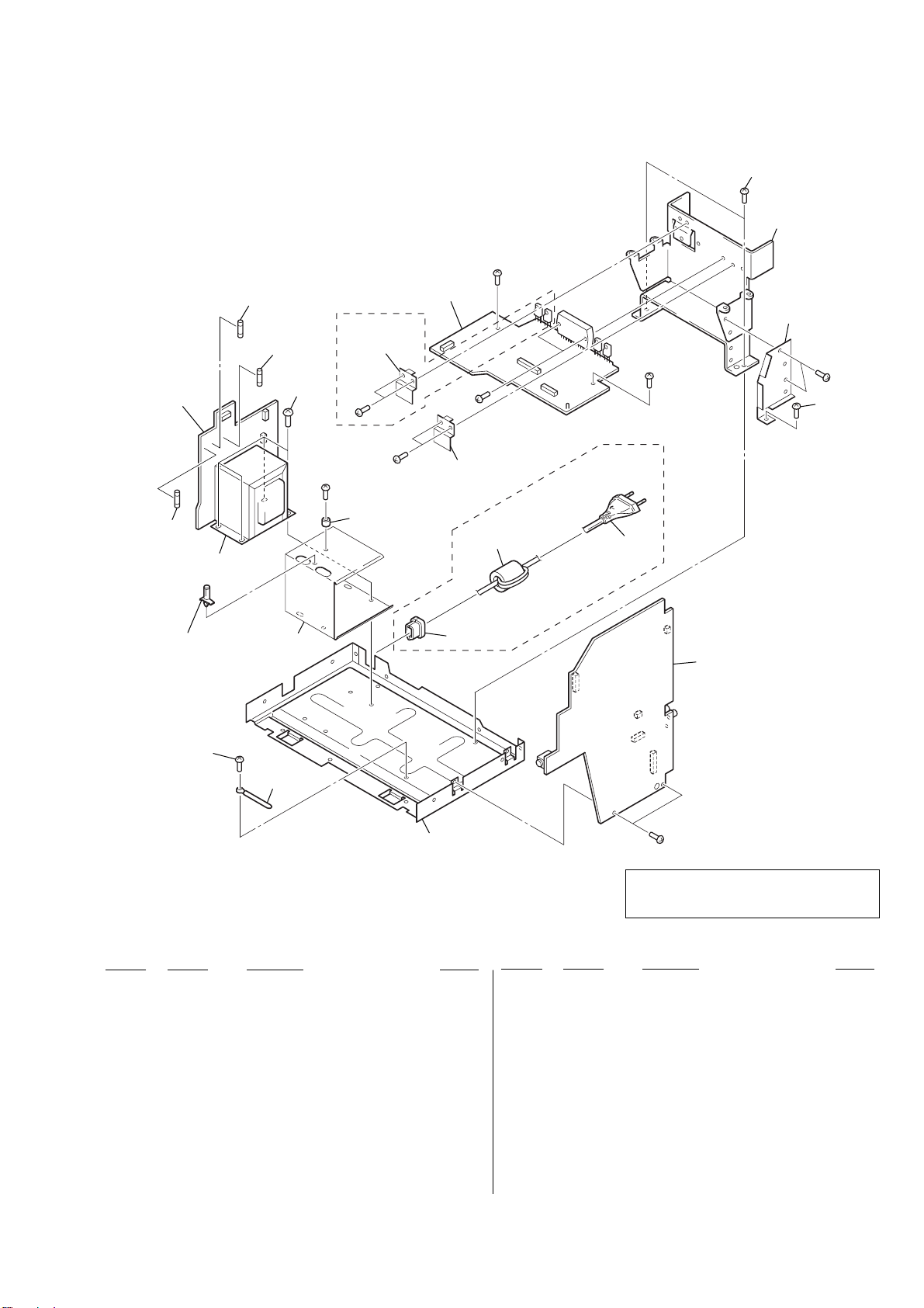
8-5. CHASSIS SECTION
CX-J3000/J3000M
202
not supplied
#1
not supplied
(PT board)
F001
PT001, PT002
not supplied
F002
F003
not supplied
203
#4
(J3000)
not supplied
#1
#1
not supplied
207
#5
not supplied
204
205
(J3000M)
206
#1
not supplied
#1
202
208
202
201
not supplied
Ref. No. Part No. Description Remark
* 201 3-703-150-11 CLAMP
202 3-970-608-11 SUMITITE (B3), +BV
203 4-900-386-01 SCREW
204 3-703-244-00 BUSHING (2104), CORD (J3000M)
205 1-500-386-11 FILTER, CLAMP (FERRITE CORE) (J3000M)
0 206 1-769-744-52 CORD, POWER (J3000M: RU, E51)
0 206 1-827-226-11 CORD, POWER (J3000M: MX)
207 A-1055-876-A AMP BOARD, COMPLETE (J3000)
207 A-1056-185-A AMP BOARD, COMPLETE (J3000M: RU)
207 A-1075-924-A AMP BOARD, COMPLETE (J3000M: E51, MX)
208 A-1055-870-A MAIN BOARD, COMPLETE (J3000)
208 A-1056-180-A MAIN BOARD, COMPLETE (J3000M: RU)
#1
The components identified by mark 0 or dotted
line with mark 0 are critical for safety.
Replace only with part number specified.
Ref. No. Part No. Description Remark
208 A-1075-922-A MAIN BOARD, COMPLETE (J3000M: E51, MX)
0 F001 1-532-504-51 FUSE (T4AL/250V) (J3000, J3000M: RU)
0 F001 1-532-505-51 FUSE (T5AL/250V) (J3000M: E51, MX)
0 F002 1-532-504-51 FUSE (T4AL/250V) (J3000, J3000M: RU)
0 F002 1-532-505-51 FUSE (T5AL/250V) (J3000M: E51, MX)
0 F003 1-532-388-51 FUSE (T2AL/250V)
0 PT001 1-443-380-11 TRANSFORMER, POWER (J3000M: E51)
0 PT002 1-443-379-11 TRANSFORMER, POWER (J3000, J3000M: RU)
0 PT002 1-443-383-11 TRANSFORMER, POWER (J3000M: MX)
#1 7-685-647-79 SCREW +BVTP 3X10 TYPE2 IT-3
#4 7-685-871-01 SCREW +BVTT 3X6 (S)
#5 7-685-650-79 SCREW +BVTP 3X16 TYPE2 IT-3
49
Page 50
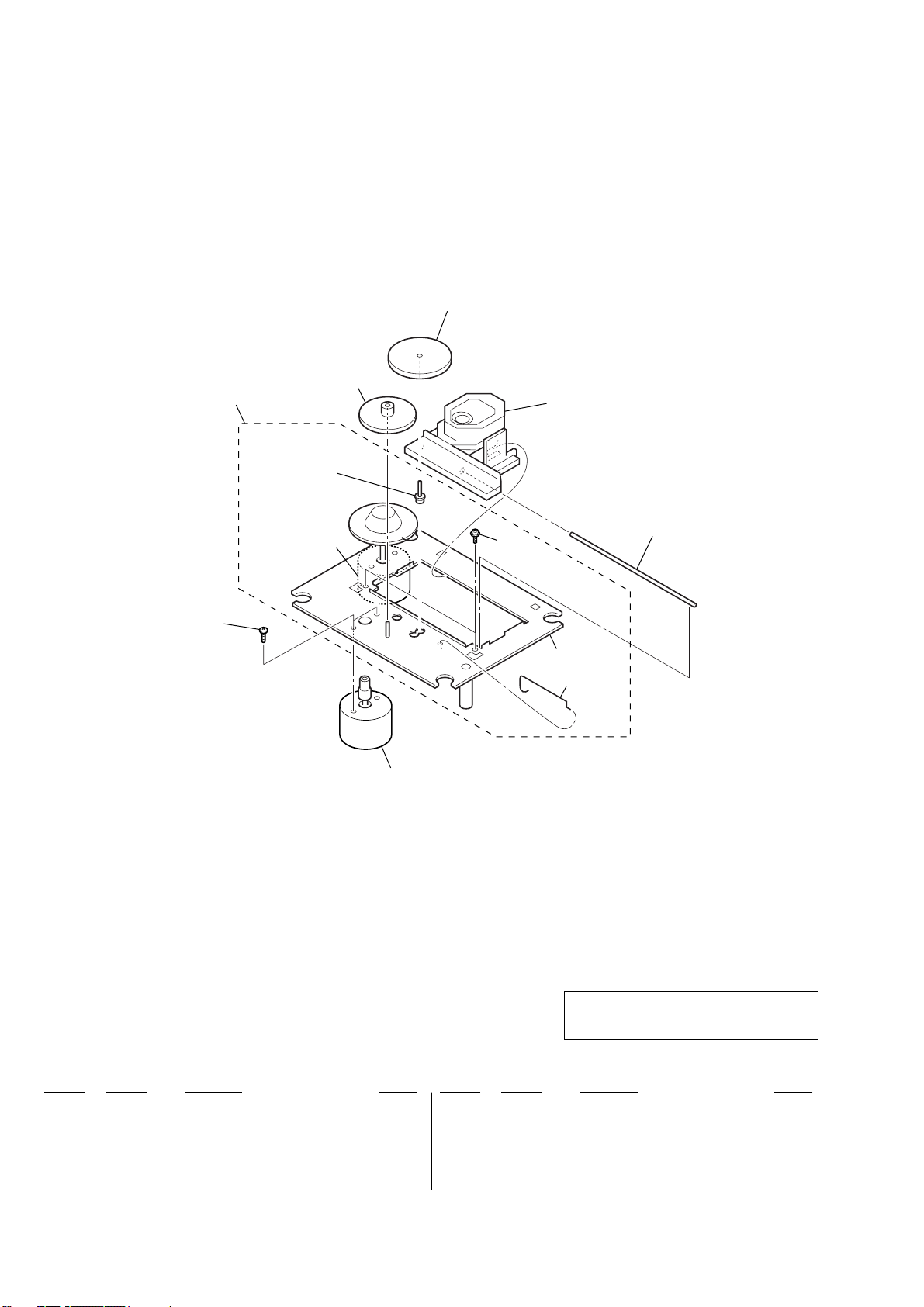
CX-J3000/J3000M
8-6. OPTICAL PICK-UP SECTION (KSM-213RDP)
553
551
(including M701 (spindle))
not supplied
M701 (spindle)
557
552
555
559
556
554
not supplied
558
M702
Ref. No. Part No. Description Remark
551 X-2162-707-2 CHASSIS ASSY (RDP) (RP), MOTOR
(including M701 (SPINDLE))
* 552 2-647-408-02 GEAR (B)
* 553 2-169-065-01 GEAR (A)
554 2-169-388-11 TAPPING (M2), +PWB
0555 8-820-161-02 OPTICAL PICK-UP (KSS-213R/C2RP)
50
The components identified by mark 0 or dotted
line with mark 0 are critical for safety.
Replace only with part number specified.
Ref. No. Part No. Description Remark
556 2-626-908-01 SHAFT, SLED
557 2-174-500-01 SCREW (2X3)
* 558 2-169-385-01 SPRING, SLED
* 559 2-169-384-01 SHAFT (S), GEAR
M702 X-2126-712-2 GEAR ASSY (R) (RP), MOTOR (SLED)
Page 51
SECTION 9
ELECTRICAL PARTS LIST
CX-J3000/J3000M
AC INLET AMP
NOTE:
• Due to standardization, replacements in the parts
list may be different from the parts specified in
the diagrams or the components used on the set.
• -XX and -X mean standardized parts, so they may
have some difference from the original one.
• RESISTORS
All resistors are in ohms.
METAL: metal-film resistor
METAL OXIDE: Metal Oxide-film resistor
F: nonflammable
•Abbreviation
E51 : Chilean and Peruvian models
MX : Mexican model
RU : Russian model
Ref. No. Part No. Description Remark Ref. No. Part No. Description Remark
AC INLET BOARD (J3000)
**************
1-533-233-31 FUSE HOLDER
< DIODE >
D001 8-719-059-21 DIODE RK46LF-T2
< JACK >
J001 1-507-563-00 JACK, DC (DC IN 12V)
0 J002 1-526-838-11 INLET, AC 2P (~AC)
< RESISTOR >
R001 1-216-833-11 METAL CHIP 10K 5% 1/10W
************************************************************
A-1055-876-A AMP BOARD, COMPLETE (J3000)
A-1056-185-A AMP BOARD, COMPLETE (J3000M: RU)
A-1075-924-A AMP BOARD, COMPLETE (J3000M: E51, MX)
********************
• Items marked “*” are not stocked since they are
seldom required for routine service. Some delay
should be anticipated when ordering these items.
• SEMICONDUCTORS
In each case, u: µ, for example:
uA... : µA... uPA... : µPA... ,
uPB... : µPB... uPC... : µPC... ,
uPD... : µPD...
• CAPACITORS:
uF: µF
• COILS
uH: µH
C168 1-104-665-11 ELECT 100uF 20% 25V
C169 1-126-934-11 ELECT 220uF 20% 16V
C170 1-131-992-11 CERAMIC CHIP 100000PF 35V
C171 1-131-992-11 CERAMIC CHIP 100000PF 35V
C172 1-131-992-11 CERAMIC CHIP 100000PF 35V
C173 1-131-992-11 CERAMIC CHIP 100000PF 35V
C201 1-126-953-11 ELECT 2200uF 20% 35V
C201 1-128-550-11 ELECT 2200uF 20% 50V
C202 1-126-953-11 ELECT 2200uF 20% 35V
C202 1-128-550-11 ELECT 2200uF 20% 50V
C203 1-164-230-11 CERAMIC CHIP 220PF 5% 50V
C204 1-164-230-11 CERAMIC CHIP 220PF 5% 50V
C207 1-126-965-11 ELECT 22uF 20% 50V
C208 1-126-965-11 ELECT 22uF 20% 50V
C209 1-126-948-11 ELECT 100uF 20% 35V
The components identified by mark
0 or dotted line with mark 0 are
critical for safety.
Replace only with part number
specified.
When indicating parts by reference
number, please include the board.
(J3000M: RU)
(EXCEPT J3000M: RU)
(J3000M: RU)
(EXCEPT J3000M: RU)
(J3000/J3000M: RU)
< CAPACITOR >
C101 1-162-964-11 CERAMIC CHIP 0.001uF 10% 50V
C102 1-107-826-11 CERAMIC CHIP 0.1uF 10% 16V
C103 1-126-933-11 ELECT 100uF 20% 16V
C104 1-126-965-11 ELECT 22uF 20% 50V
(J3000)
C106 1-126-960-11 ELECT 1uF 20% 50V
C107 1-126-947-11 ELECT 47uF 20% 35V
C108 1-126-947-11 ELECT 47uF 20% 35V
C151 1-131-992-11 CERAMIC CHIP 100000PF 35V
C152 1-131-992-11 CERAMIC CHIP 100000PF 35V
C153 1-131-992-11 CERAMIC CHIP 100000PF 35V
C154 1-131-992-11 CERAMIC CHIP 100000PF 35V
C155 1-131-992-11 CERAMIC CHIP 100000PF 35V
C156 1-131-992-11 CERAMIC CHIP 100000PF 35V
C157 1-131-992-11 CERAMIC CHIP 100000PF 35V
C158 1-131-992-11 CERAMIC CHIP 100000PF 35V
C159 1-126-934-11 ELECT 220uF 20% 16V
C160 1-126-943-11 ELECT 2200uF 20% 25V
C161 1-162-964-11 CERAMIC CHIP 0.001uF 10% 50V
C162 1-107-826-11 CERAMIC CHIP 0.1uF 10% 16V
C163 1-126-934-11 ELECT 220uF 20% 16V
C209 1-126-968-11 ELECT 100uF 20% 50V
(J3000M: E51, MX)
C210 1-126-964-11 ELECT 10uF 20% 50V
C211 1-126-964-11 ELECT 10uF 20% 50V
C212 1-126-963-11 ELECT 4.7uF 20% 50V
(J3000)
C213 1-126-960-11 ELECT 1uF 20% 50V
(J3000)
C214 1-126-960-11 ELECT 1uF 20% 50V
(J3000)
C215 1-126-933-11 ELECT 100uF 20% 16V
(J3000)
C216 1-104-665-11 ELECT 100uF 20% 25V
(J3000)
C217 1-162-915-11 CERAMIC CHIP 10PF 0.5PF 50V
C218 1-162-915-11 CERAMIC CHIP 10PF 0.5PF 50V
C219 1-104-665-11 ELECT 100uF 20% 25V
C220 1-162-964-11 CERAMIC CHIP 0.001uF 10% 50V
(J3000)
C223 1-162-927-11 CERAMIC CHIP 100PF 5% 50V
C224 1-162-927-11 CERAMIC CHIP 100PF 5% 50V
C225 1-126-963-11 ELECT 4.7uF 20% 50V
C226 1-126-963-11 ELECT 4.7uF 20% 50V
51
Page 52

CX-J3000/J3000M
AMP
Ref. No. Part No. Description Remark
C227 1-136-171-00 FILM 0.33uF 5% 50V
C228 1-136-171-00 FILM 0.33uF 5% 50V
C229 1-162-964-11 CERAMIC CHIP 0.001uF 10% 50V
(J3000)
C230 1-162-964-11 CERAMIC CHIP 0.001uF 10% 50V
(J3000)
C233 1-126-767-11 ELECT 1000uF 20% 16V
(J3000)
C234 1-126-767-11 ELECT 1000uF 20% 16V
(J3000)
C235 1-162-964-11 CERAMIC CHIP 0.001uF 10% 50V
(J3000)
C236 1-162-964-11 CERAMIC CHIP 0.001uF 10% 50V
(J3000)
C237 1-107-826-11 CERAMIC CHIP 0.1uF 10% 16V
C238 1-126-948-11 ELECT 100uF 20% 35V
(J3000/J3000M: RU)
C238 1-126-968-11 ELECT 100uF 20% 50V
(J3000M: E51, MX)
C249 1-107-826-11 CERAMIC CHIP 0.1uF 10% 16V
C257 1-136-171-00 FILM 0.33uF 5% 50V
C258 1-136-171-00 FILM 0.33uF 5% 50V
< CONNECTOR >
CN102 1-784-774-11 CONNECTOR, FFC 13P (J3000M)
CN102 1-784-776-11 CONNECTOR, FFC 15P (J3000)
* CN201 1-764-334-11 PLUG, CONNECTOR 11P (J3000M)
* CN201 1-564-516-11 PLUG, CONNECTOR 13P (J3000)
* CN206 1-564-187-00 PIN, CONNECTOR
Ref. No. Part No. Description Remark
< EARTH TERMINAL >
* EP201 1-537-738-21 TERMINAL, EARTH
< IC >
IC201 8-759-452-80 IC LA4600 (J3000)
IC202 6-705-620-01 IC STK433-060 (J3000M: E51, MX)
IC202 6-705-854-01 IC STK433-030 (J3000/J3000M: RU)
< SHORT >
JR204 1-216-864-11 SHORT CHIP 0
< CAPACITOR >
JW115 1-127-876-21 CERAMIC 0.01uF 10% 50V
(J3000M)
< TRANSISTOR >
Q101 8-729-209-60 TRANSISTOR 2SB1375
Q102 8-729-120-28 TRANSISTOR 2SC1623-L5L6
Q103 8-729-120-28 TRANSISTOR 2SC1623-L5L6
Q104 6-550-580-01 TRANSISTOR 2SA1235TP-1F
Q151 8-729-209-60 TRANSISTOR 2SB1375
Q152 8-729-120-28 TRANSISTOR 2SC1623-L5L6
Q153 8-729-120-28 TRANSISTOR 2SC1623-L5L6
Q154 6-550-305-01 TRANSISTOR 2SA1296GR-(TPE2)
Q155 8-729-027-46 TRANSISTOR DTC114YKA-T146
Q157 8-729-209-60 TRANSISTOR 2SB1375
< DIODE >
D101 8-719-991-33 DIODE 1SS133T-77
D102 8-719-109-97 DIODE RD6.8ESB2
D104 8-719-991-33 DIODE 1SS133T-77
D105 8-719-991-33 DIODE 1SS133T-77
D106 8-719-991-33 DIODE 1SS133T-77
D151 8-719-046-07 DIODE 2A02M
D152 8-719-046-07 DIODE 2A02M
D153 8-719-046-07 DIODE 2A02M
D154 8-719-046-07 DIODE 2A02M
D155 8-719-046-47 DIODE 1N5401TM
D156 8-719-046-47 DIODE 1N5401TM
D157 8-719-046-47 DIODE 1N5401TM
D158 8-719-046-47 DIODE 1N5401TM
D160 8-719-991-33 DIODE 1SS133T-77
D161 8-719-109-85 DIODE RD5.1ESB2
D163 8-719-982-01 DIODE MTZJ-3.3B
D164 8-719-991-33 DIODE 1SS133T-77
D170 8-719-991-33 DIODE 1SS133T-77
D173 8-719-982-01 DIODE MTZJ-3.3B
D176 8-719-991-33 DIODE 1SS133T-77
D201 8-719-991-33 DIODE 1SS133T-77
D202 8-719-991-33 DIODE 1SS133T-77
D203 8-719-109-85 DIODE RD5.1ESB2
D204 8-719-991-33 DIODE 1SS133T-77
D205 8-719-991-33 DIODE 1SS133T-77
D206 8-719-991-33 DIODE 1SS133T-77
Q158 8-729-120-28 TRANSISTOR 2SC1623-L5L6
Q160 8-729-120-28 TRANSISTOR 2SC1623-L5L6
Q201 6-550-580-01 TRANSISTOR 2SA1235TP-1F
Q202 6-550-580-01 TRANSISTOR 2SA1235TP-1F
Q203 8-729-120-28 TRANSISTOR 2SC1623-L5L6
Q204 8-729-120-28 TRANSISTOR 2SC1623-L5L6
Q205 8-729-120-28 TRANSISTOR 2SC1623-L5L6
Q206 8-729-120-28 TRANSISTOR 2SC1623-L5L6
Q207 6-550-580-01 TRANSISTOR 2SA1235TP-1F
Q208 8-729-048-99 FET 2SK2541-T
Q209 6-550-580-01 TRANSISTOR 2SA1235TP-1F
Q251 8-729-120-28 TRANSISTOR 2SC1623-L5L6
Q252 8-729-120-28 TRANSISTOR 2SC1623-L5L6
Q253 6-550-580-01 TRANSISTOR 2SA1235TP-1F
Q254 8-729-120-28 TRANSISTOR 2SC1623-L5L6
< RESISTOR >
R101 1-216-809-11 METAL CHIP 100 5% 1/10W
R102 1-216-807-11 METAL CHIP 68 5% 1/10W
R103 1-216-829-11 METAL CHIP 4.7K 5% 1/10W
R104 1-216-823-11 METAL CHIP 1.5K 5% 1/10W
R105 1-216-817-11 METAL CHIP 470 5% 1/10W
R106 1-216-821-11 METAL CHIP 1K 5% 1/10W
(J3000)
R107 1-216-809-11 METAL CHIP 100 5% 1/10W
R109 1-216-821-11 METAL CHIP 1K 5% 1/10W
(J3000)
R110 1-216-809-11 METAL CHIP 100 5% 1/10W
R111 1-216-829-11 METAL CHIP 4.7K 5% 1/10W
52
Page 53

CX-J3000/J3000M
AMP
Ref. No. Part No. Description Remark
R112 1-216-828-11 METAL CHIP 3.9K 5% 1/10W
(J3000)
R112 1-216-830-11 METAL CHIP 5.6K 5% 1/10W
(J3000M)
R113 1-216-825-11 METAL CHIP 2.2K 5% 1/10W
R115 1-216-821-11 METAL CHIP 1K 5% 1/10W
R116 1-216-821-11 METAL CHIP 1K 5% 1/10W
R117 1-216-837-11 METAL CHIP 22K 5% 1/10W
R118 1-216-825-11 METAL CHIP 2.2K 5% 1/10W
R119 1-216-825-11 METAL CHIP 2.2K 5% 1/10W
R120 1-216-841-11 METAL CHIP 47K 5% 1/10W
R122 1-216-829-11 METAL CHIP 4.7K 5% 1/10W
R154 1-216-833-11 METAL CHIP 10K 5% 1/10W
(J3000)
R155 1-216-825-11 METAL CHIP 2.2K 5% 1/10W
(J3000)
R156 1-216-827-11 METAL CHIP 3.3K 5% 1/10W
(J3000)
R157 1-216-809-11 METAL CHIP 100 5% 1/10W
R158 1-216-807-11 METAL CHIP 68 5% 1/10W
R159 1-216-829-11 METAL CHIP 4.7K 5% 1/10W
R160 1-216-823-11 METAL CHIP 1.5K 5% 1/10W
R161 1-216-817-11 METAL CHIP 470 5% 1/10W
R162 1-216-821-11 METAL CHIP 1K 5% 1/10W
R163 1-216-841-11 METAL CHIP 47K 5% 1/10W
R164 1-249-413-11 CARBON 470 5% 1/4W
R166 1-249-413-11 CARBON 470 5% 1/4W
R167 1-247-807-31 CARBON 100 5% 1/4W
R168 1-216-809-11 METAL CHIP 100 5% 1/10W
R169 1-216-841-11 METAL CHIP 47K 5% 1/10W
R170 1-216-809-11 METAL CHIP 100 5% 1/10W
R171 1-216-817-11 METAL CHIP 470 5% 1/10W
R173 1-216-853-11 METAL CHIP 470K 5% 1/10W
R174 1-216-821-11 METAL CHIP 1K 5% 1/10W
R201 1-216-833-11 METAL CHIP 10K 5% 1/10W
R202 1-216-833-11 METAL CHIP 10K 5% 1/10W
0 R203 1-216-361-31 METAL OXIDE 0.22 5% 2W F
0 R204 1-216-361-31 METAL OXIDE 0.22 5% 2W F
R205 1-216-821-11 METAL CHIP 1K 5% 1/10W
R206 1-216-821-11 METAL CHIP 1K 5% 1/10W
R207 1-216-833-11 METAL CHIP 10K 5% 1/10W
R208 1-216-833-11 METAL CHIP 10K 5% 1/10W
R209 1-216-835-11 METAL CHIP 15K 5% 1/10W
R210 1-216-835-11 METAL CHIP 15K 5% 1/10W
R211 1-216-853-11 METAL CHIP 470K 5% 1/10W
R212 1-216-845-11 METAL CHIP 100K 5% 1/10W
R213 1-216-845-11 METAL CHIP 100K 5% 1/10W
R214 1-216-826-11 METAL CHIP 2.7K 5% 1/10W
(J3000)
R215 1-216-826-11 METAL CHIP 2.7K 5% 1/10W
(J3000)
R216 1-216-837-11 METAL CHIP 22K 5% 1/10W
R217 1-216-841-11 METAL CHIP 47K 5% 1/10W
R218 1-216-841-11 METAL CHIP 47K 5% 1/10W
0 R219 1-202-972-61 FUSIBLE 1 5% 1/4W F
0 R220 1-202-972-61 FUSIBLE 1 5% 1/4W F
R221 1-216-833-11 METAL CHIP 10K 5% 1/10W
R222 1-216-821-11 METAL CHIP 1K 5% 1/10W
R225 1-216-836-11 METAL CHIP 18K 5% 1/10W
Ref. No. Part No. Description Remark
R226 1-216-836-11 METAL CHIP 18K 5% 1/10W
R227 1-216-864-11 SHORT CHIP 0
R228 1-216-864-11 SHORT CHIP 0
R229 1-216-833-11 METAL CHIP 10K 5% 1/10W
R230 1-216-833-11 METAL CHIP 10K 5% 1/10W
R231 1-216-833-11 METAL CHIP 10K 5% 1/10W
R232 1-216-853-11 METAL CHIP 470K 5% 1/10W
(J3000)
0 R233 1-212-881-11 FUSIBLE 100 5% 1/4W F
R234 1-216-829-11 METAL CHIP 4.7K 5% 1/10W
(J3000)
R235 1-216-829-11 METAL CHIP 4.7K 5% 1/10W
R236 1-216-833-11 METAL CHIP 10K 5% 1/10W
R237 1-216-839-11 METAL CHIP 33K 5% 1/10W
R238 1-216-829-11 METAL CHIP 4.7K 5% 1/10W
R239 1-216-841-11 METAL CHIP 47K 5% 1/10W
(J3000)
R240 1-216-841-11 METAL CHIP 47K 5% 1/10W
(J3000)
R241 1-216-829-11 METAL CHIP 4.7K 5% 1/10W
R243 1-216-821-11 METAL CHIP 1K 5% 1/10W
(J3000M: E51, MX)
R244 1-216-821-11 METAL CHIP 1K 5% 1/10W
(J3000M: E51, MX)
R245 1-249-409-11 CARBON 220 5% 1/4W
(J3000)
R246 1-249-409-11 CARBON 220 5% 1/4W
(J3000)
R247 1-260-103-11 CARBON 2.2K 5% 1/2W
(J3000)
R248 1-260-103-11 CARBON 2.2K 5% 1/2W
(J3000)
R251 1-216-825-11 METAL CHIP 2.2K 5% 1/10W
R252 1-216-825-11 METAL CHIP 2.2K 5% 1/10W
R253 1-216-822-11 METAL CHIP 1.2K 5% 1/10W
(J3000M: E51, MX)
R253 1-216-823-11 METAL CHIP 1.5K 5% 1/10W
(J3000/J3000M: RU)
R254 1-216-822-11 METAL CHIP 1.2K 5% 1/10W
(J3000M: E51, MX)
R254 1-216-823-11 METAL CHIP 1.5K 5% 1/10W
(J3000/J3000M: RU)
R255 1-216-841-11 METAL CHIP 47K 5% 1/10W
R256 1-216-841-11 METAL CHIP 47K 5% 1/10W
R257 1-216-841-11 METAL CHIP 47K 5% 1/10W
R258 1-216-841-11 METAL CHIP 47K 5% 1/10W
0 R259 1-212-881-11 FUSIBLE 100 5% 1/4W F
R267 1-260-296-11 CARBON 2.2 5% 1/2W
R268 1-260-296-11 CARBON 2.2 5% 1/2W
R269 1-216-821-11 METAL CHIP 1K 5% 1/10W
R270 1-216-821-11 METAL CHIP 1K 5% 1/10W
R272 1-216-841-11 METAL CHIP 47K 5% 1/10W
R273 1-260-083-11 CARBON 47 5% 1/2W
(J3000M)
R273 1-260-085-11 CARBON 68 5% 1/2W
(J3000)
R277 1-216-857-11 METAL CHIP 1M 5% 1/10W
R278 1-216-841-11 METAL CHIP 47K 5% 1/10W
R279 1-216-837-11 METAL CHIP 22K 5% 1/10W
R280 1-216-833-11 METAL CHIP 10K 5% 1/10W
The components identified by mark 0 or dotted
line with mark 0 are critical for safety.
Replace only with part number specified.
53
Page 54

CX-J3000/J3000M
CDBACK LIGHT
Ref. No. Part No. Description Remark
< THERMISTOR >
TH202 1-807-796-11 THERMISTOR
************************************************************
BACK LIGHT BOARD
****************
< LED >
D812 6-500-424-01 LED SLI-325DCT31W (LCD BACK LIGHT)
D813 6-500-424-01 LED SLI-325DCT31W (LCD BACK LIGHT)
D814 6-500-424-01 LED SLI-325DCT31W (LCD BACK LIGHT)
D815 6-500-424-01 LED SLI-325DCT31W (LCD BACK LIGHT)
D816 6-500-424-01 LED SLI-325DCT31W (LCD BACK LIGHT)
D817 6-500-424-01 LED SLI-325DCT31W (LCD BACK LIGHT)
< RESISTOR >
R1836 1-216-809-11 METAL CHIP 100 5% 1/10W
R1837 1-216-809-11 METAL CHIP 100 5% 1/10W
R1838 1-216-809-11 METAL CHIP 100 5% 1/10W
R1839 1-216-809-11 METAL CHIP 100 5% 1/10W
************************************************************
* A-3683-956-A CD BOARD, COMPLETE (J3000)
*******************
< CAPACITOR >
C701 1-162-964-11 CERAMIC CHIP 0.001uF 10% 50V
C702 1-126-947-11 ELECT 47uF 20% 35V
C703 1-107-826-11 CERAMIC CHIP 0.1uF 10% 16V
C704 1-162-919-11 CERAMIC CHIP 22PF 5% 50V
C705 1-162-968-11 CERAMIC CHIP 0.0047uF 10% 50V
Ref. No. Part No. Description Remark
C740 1-126-935-11 ELECT 470uF 20% 16V
C741 1-164-156-11 CERAMIC CHIP 0.1uF 25V
C742 1-164-156-11 CERAMIC CHIP 0.1uF 25V
C743 1-164-156-11 CERAMIC CHIP 0.1uF 25V
C744 1-164-156-11 CERAMIC CHIP 0.1uF 25V
C745 1-164-156-11 CERAMIC CHIP 0.1uF 25V
C746 1-104-665-11 ELECT 100uF 20% 25V
C747 1-104-665-11 ELECT 100uF 20% 25V
C750 1-104-665-11 ELECT 100uF 20% 25V
C751 1-164-156-11 CERAMIC CHIP 0.1uF 25V
C754 1-162-970-11 CERAMIC CHIP 0.01uF 10% 25V
C755 1-162-970-11 CERAMIC CHIP 0.01uF 10% 25V
< CONNECTOR >
CNP701 1-779-553-21 CONNECTOR, FFC (LIF (NON-ZIF)) 16P
* CNP702 1-784-736-11 CONNECTOR, FFC 14P
< FERRITE BEAD >
FB701 1-469-701-21 FERRITE, EMI (SMD) (1608)
< IC >
IC701 6-701-796-01 IC LC78646E-US-E
IC702 6-701-787-11 IC BA5826FP-E2
< RESISTOR >
JC701 1-216-864-11 SHORT CHIP 0
JC702 1-216-864-11 SHORT CHIP 0
JC703 1-216-864-11 SHORT CHIP 0
JC704 1-216-821-11 METAL CHIP 1K 5% 1/10W
< FERRITE BEAD >
C706 1-126-960-11 ELECT 1uF 20% 50V
C707 1-115-156-11 CERAMIC CHIP 1uF 10V
C708 1-162-927-11 CERAMIC CHIP 100PF 5% 50V
C709 1-164-156-11 CERAMIC CHIP 0.1uF 25V
C711 1-162-974-11 CERAMIC CHIP 0.01uF 50V
C716 1-162-974-11 CERAMIC CHIP 0.01uF 50V
C717 1-163-021-11 CERAMIC CHIP 0.01uF 10% 50V
C720 1-162-919-11 CERAMIC CHIP 22PF 5% 50V
C721 1-162-919-11 CERAMIC CHIP 22PF 5% 50V
C722 1-162-919-11 CERAMIC CHIP 22PF 5% 50V
C723 1-162-974-11 CERAMIC CHIP 0.01uF 50V
C724 1-162-919-11 CERAMIC CHIP 22PF 5% 50V
C725 1-162-964-11 CERAMIC CHIP 0.001uF 10% 50V
C726 1-162-964-11 CERAMIC CHIP 0.001uF 10% 50V
C727 1-162-964-11 CERAMIC CHIP 0.001uF 10% 50V
C728 1-165-176-11 CERAMIC CHIP 0.047uF 10% 16V
C729 1-125-837-11 CERAMIC CHIP 1uF 10% 6.3V
C730 1-107-826-11 CERAMIC CHIP 0.1uF 10% 16V
C731 1-165-176-11 CERAMIC CHIP 0.047uF 10% 16V
C732 1-104-665-11 ELECT 100uF 20% 25V
C733 1-104-665-11 ELECT 100uF 20% 25V
C734 1-162-968-11 CERAMIC CHIP 0.0047uF 10% 50V
C735 1-126-916-11 ELECT 1000uF 20% 6.3V
C736 1-162-968-11 CERAMIC CHIP 0.0047uF 10% 50V
C738 1-164-156-11 CERAMIC CHIP 0.1uF 25V
C739 1-164-156-11 CERAMIC CHIP 0.1uF 25V
L706 1-414-445-11 FERRITE, EMI (SMD) (1608)
< TRANSISTOR >
Q701 8-729-054-57 TRANSISTOR KTN2907AS-RTK
< RESISTOR >
R701 1-216-841-11 METAL CHIP 47K 5% 1/10W
R702 1-216-835-11 METAL CHIP 15K 5% 1/10W
R703 1-216-835-11 METAL CHIP 15K 5% 1/10W
R704 1-216-835-11 METAL CHIP 15K 5% 1/10W
R705 1-216-835-11 METAL CHIP 15K 5% 1/10W
R706 1-216-841-11 METAL CHIP 47K 5% 1/10W
R707 1-216-797-11 METAL CHIP 10 5% 1/10W
R708 1-216-833-11 METAL CHIP 10K 5% 1/10W
R709 1-216-837-11 METAL CHIP 22K 5% 1/10W
R710 1-216-829-11 METAL CHIP 4.7K 5% 1/10W
R711 1-216-815-11 METAL CHIP 330 5% 1/10W
R712 1-216-809-11 METAL CHIP 100 5% 1/10W
R714 1-216-811-11 METAL CHIP 150 5% 1/10W
R715 1-216-811-11 METAL CHIP 150 5% 1/10W
R716 1-216-821-11 METAL CHIP 1K 5% 1/10W
R717 1-216-821-11 METAL CHIP 1K 5% 1/10W
R718 1-216-821-11 METAL CHIP 1K 5% 1/10W
R719 1-216-809-11 METAL CHIP 100 5% 1/10W
R720 1-216-809-11 METAL CHIP 100 5% 1/10W
R721 1-216-821-11 METAL CHIP 1K 5% 1/10W
54
Page 55

CX-J3000/J3000M
CD CD/MP3
Ref. No. Part No. Description Remark
R722 1-216-809-11 METAL CHIP 100 5% 1/10W
R723 1-216-809-11 METAL CHIP 100 5% 1/10W
R724 1-216-841-11 METAL CHIP 47K 5% 1/10W
R725 1-216-819-11 METAL CHIP 680 5% 1/10W
R726 1-216-819-11 METAL CHIP 680 5% 1/10W
R727 1-216-825-11 METAL CHIP 2.2K 5% 1/10W
R728 1-216-833-11 METAL CHIP 10K 5% 1/10W
R729 1-216-813-11 METAL CHIP 220 5% 1/10W
R730 1-216-821-11 METAL CHIP 1K 5% 1/10W
R731 1-216-825-11 METAL CHIP 2.2K 5% 1/10W
R732 1-216-841-11 METAL CHIP 47K 5% 1/10W
R741 1-218-867-11 METAL CHIP 6.8K 0.5% 1/10W
R743 1-218-867-11 METAL CHIP 6.8K 0.5% 1/10W
R744 1-216-845-11 METAL CHIP 100K 5% 1/10W
< SWITCH >
S701 1-571-936-11 SWITCH, LEAF (LIMIT)
< VIBRATOR >
X701 1-781-801-21 VIBRATOR, CERAMIC (16.9344MHz)
************************************************************
* A-3347-681-A CD/MP3 BOARD, COMPLETE (J3000M)
***********************
< CAPACITOR >
C701 1-164-156-11 CERAMIC CHIP 0.1uF 25V
C702 1-104-665-11 ELECT 100uF 20% 25V
C703 1-164-156-11 CERAMIC CHIP 0.1uF 25V
C704 1-126-947-11 ELECT 47uF 20% 35V
C705 1-162-964-11 CERAMIC CHIP 0.001uF 10% 50V
C706 1-164-156-11 CERAMIC CHIP 0.1uF 25V
C707 1-104-665-11 ELECT 100uF 20% 25V
C708 1-107-826-11 CERAMIC CHIP 0.1uF 10% 16V
C709 1-104-665-11 ELECT 100uF 20% 25V
C710 1-165-176-11 CERAMIC CHIP 0.047uF 10% 16V
C711 1-107-826-11 CERAMIC CHIP 0.1uF 10% 16V
C712 1-162-923-11 CERAMIC CHIP 47PF 5% 50V
C713 1-162-968-11 CERAMIC CHIP 0.0047uF 10% 50V
C714 1-164-156-11 CERAMIC CHIP 0.1uF 25V
C715 1-126-960-11 ELECT 1uF 20% 50V
C716 1-162-964-11 CERAMIC CHIP 0.001uF 10% 50V
C717 1-162-968-11 CERAMIC CHIP 0.0047uF 10% 50V
C718 1-115-156-11 CERAMIC CHIP 1uF 10V
C719 1-162-968-11 CERAMIC CHIP 0.0047uF 10% 50V
C720 1-162-927-11 CERAMIC CHIP 100PF 5% 50V
C721 1-164-156-11 CERAMIC CHIP 0.1uF 25V
C722 1-164-156-11 CERAMIC CHIP 0.1uF 25V
C723 1-104-665-11 ELECT 100uF 20% 25V
C729 1-126-916-11 ELECT 1000uF 20% 6.3V
C731 1-162-968-11 CERAMIC CHIP 0.0047uF 10% 50V
C732 1-162-970-11 CERAMIC CHIP 0.01uF 10% 25V
C733 1-162-970-11 CERAMIC CHIP 0.01uF 10% 25V
C734 1-162-968-11 CERAMIC CHIP 0.0047uF 10% 50V
C737 1-162-970-11 CERAMIC CHIP 0.01uF 10% 25V
C740 1-164-156-11 CERAMIC CHIP 0.1uF 25V
C741 1-115-156-11 CERAMIC CHIP 1uF 10V
Ref. No. Part No. Description Remark
C742 1-164-156-11 CERAMIC CHIP 0.1uF 25V
C743 1-165-176-11 CERAMIC CHIP 0.047uF 10% 16V
C744 1-115-156-11 CERAMIC CHIP 1uF 10V
C745 1-162-923-11 CERAMIC CHIP 47PF 5% 50V
C746 1-164-156-11 CERAMIC CHIP 0.1uF 25V
C747 1-164-156-11 CERAMIC CHIP 0.1uF 25V
C748 1-126-935-11 ELECT 470uF 20% 16V
C750 1-162-919-11 CERAMIC CHIP 22PF 5% 50V
C751 1-162-923-11 CERAMIC CHIP 47PF 5% 50V
C753 1-162-923-11 CERAMIC CHIP 47PF 5% 50V
C754 1-162-923-11 CERAMIC CHIP 47PF 5% 50V
C756 1-162-923-11 CERAMIC CHIP 47PF 5% 50V
C760 1-162-923-11 CERAMIC CHIP 47PF 5% 50V
C761 1-162-923-11 CERAMIC CHIP 47PF 5% 50V
C762 1-162-923-11 CERAMIC CHIP 47PF 5% 50V
C763 1-162-923-11 CERAMIC CHIP 47PF 5% 50V
C764 1-162-923-11 CERAMIC CHIP 47PF 5% 50V
C766 1-162-923-11 CERAMIC CHIP 47PF 5% 50V
C767 1-162-919-11 CERAMIC CHIP 22PF 5% 50V
C1001 1-162-923-11 CERAMIC CHIP 47PF 5% 50V
C1010 1-164-156-11 CERAMIC CHIP 0.1uF 25V
C1011 1-164-156-11 CERAMIC CHIP 0.1uF 25V
C1012 1-115-156-11 CERAMIC CHIP 1uF 10V
C1013 1-164-156-11 CERAMIC CHIP 0.1uF 25V
C1014 1-104-665-11 ELECT 100uF 20% 25V
C1029 1-126-916-11 ELECT 1000uF 20% 6.3V
C1030 1-164-156-11 CERAMIC CHIP 0.1uF 25V
C1031 1-164-156-11 CERAMIC CHIP 0.1uF 25V
C1037 1-164-156-11 CERAMIC CHIP 0.1uF 25V
C1042 1-104-665-11 ELECT 100uF 20% 25V
C1043 1-164-156-11 CERAMIC CHIP 0.1uF 25V
C1044 1-164-156-11 CERAMIC CHIP 0.1uF 25V
C1054 1-126-935-11 ELECT 470uF 20% 16V
C1055 1-164-156-11 CERAMIC CHIP 0.1uF 25V
C1056 1-115-156-11 CERAMIC CHIP 1uF 10V
C1057 1-162-923-11 CERAMIC CHIP 47PF 5% 50V
C1058 1-162-923-11 CERAMIC CHIP 47PF 5% 50V
C1059 1-162-923-11 CERAMIC CHIP 47PF 5% 50V
C1066 1-162-923-11 CERAMIC CHIP 47PF 5% 50V
C1067 1-162-923-11 CERAMIC CHIP 47PF 5% 50V
C1068 1-162-923-11 CERAMIC CHIP 47PF 5% 50V
C1069 1-162-923-11 CERAMIC CHIP 47PF 5% 50V
C1070 1-162-923-11 CERAMIC CHIP 47PF 5% 50V
C1074 1-162-919-11 CERAMIC CHIP 22PF 5% 50V
< CONNECTOR >
CNP701 1-779-553-21 CONNECTOR, FFC (LIF (NON-ZIF)) 16P
CNP702 1-784-742-11 CONNECTOR, FFC 20P
< FERRITE BEAD >
FB701 1-469-701-21 FERRITE, EMI (SMD) (1608)
FB702 1-469-701-21 FERRITE, EMI (SMD) (1608)
FB703 1-469-701-21 FERRITE, EMI (SMD) (1608)
FB704 1-469-701-21 FERRITE, EMI (SMD) (1608)
FB705 1-469-701-21 FERRITE, EMI (SMD) (1608)
FB706 1-469-701-21 FERRITE, EMI (SMD) (1608)
FB707 1-469-701-21 FERRITE, EMI (SMD) (1608)
FB1001 1-469-701-21 FERRITE, EMI (SMD) (1608)
55
Page 56

CX-J3000/J3000M
MAINCD/MP3
Ref. No. Part No. Description Remark
FB1002 1-469-701-21 FERRITE, EMI (SMD) (1608)
< IC >
IC701 6-701-796-01 IC LC78646E-US-E
IC702 6-701-787-11 IC BA5826FP-E2
IC1001 6-704-008-01 IC LC78684E-US-E
IC1002 6-704-009-01 IC LC32V4265CT-25-MPB-E
IC1003 6-704-059-01 IC S-817B18AMC-CWHT2G
< TRANSISTOR >
Q701 8-729-054-57 TRANSISTOR KTN2907AS-RTK
< RESISTOR >
R701 1-216-841-11 METAL CHIP 47K 5% 1/10W
R702 1-216-833-11 METAL CHIP 10K 5% 1/10W
R703 1-216-833-11 METAL CHIP 10K 5% 1/10W
R704 1-216-833-11 METAL CHIP 10K 5% 1/10W
R705 1-216-833-11 METAL CHIP 10K 5% 1/10W
R706 1-216-841-11 METAL CHIP 47K 5% 1/10W
R707 1-216-797-11 METAL CHIP 10 5% 1/10W
R708 1-216-833-11 METAL CHIP 10K 5% 1/10W
R709 1-216-837-11 METAL CHIP 22K 5% 1/10W
R710 1-216-829-11 METAL CHIP 4.7K 5% 1/10W
R711 1-216-813-11 METAL CHIP 220 5% 1/10W
R712 1-216-825-11 METAL CHIP 2.2K 5% 1/10W
R713 1-216-821-11 METAL CHIP 1K 5% 1/10W
R714 1-216-809-11 METAL CHIP 100 5% 1/10W
R715 1-216-809-11 METAL CHIP 100 5% 1/10W
R716 1-216-809-11 METAL CHIP 100 5% 1/10W
R717 1-216-809-11 METAL CHIP 100 5% 1/10W
R718 1-216-809-11 METAL CHIP 100 5% 1/10W
R719 1-216-809-11 METAL CHIP 100 5% 1/10W
R720 1-216-809-11 METAL CHIP 100 5% 1/10W
R721 1-216-809-11 METAL CHIP 100 5% 1/10W
R722 1-216-809-11 METAL CHIP 100 5% 1/10W
R723 1-216-809-11 METAL CHIP 100 5% 1/10W
R724 1-216-841-11 METAL CHIP 47K 5% 1/10W
R725 1-216-817-11 METAL CHIP 470 5% 1/10W
R726 1-216-817-11 METAL CHIP 470 5% 1/10W
R727 1-216-825-11 METAL CHIP 2.2K 5% 1/10W
R728 1-216-833-11 METAL CHIP 10K 5% 1/10W
R729 1-216-813-11 METAL CHIP 220 5% 1/10W
R730 1-216-821-11 METAL CHIP 1K 5% 1/10W
R731 1-216-825-11 METAL CHIP 2.2K 5% 1/10W
R732 1-216-809-11 METAL CHIP 100 5% 1/10W
R733 1-216-809-11 METAL CHIP 100 5% 1/10W
R734 1-216-809-11 METAL CHIP 100 5% 1/10W
R735 1-216-809-11 METAL CHIP 100 5% 1/10W
R736 1-216-809-11 METAL CHIP 100 5% 1/10W
R737 1-216-809-11 METAL CHIP 100 5% 1/10W
R740 1-216-809-11 METAL CHIP 100 5% 1/10W
R743 1-216-829-11 METAL CHIP 4.7K 5% 1/10W
R744 1-216-845-11 METAL CHIP 100K 5% 1/10W
R745 1-216-809-11 METAL CHIP 100 5% 1/10W
R753 1-216-829-11 METAL CHIP 4.7K 5% 1/10W
R755 1-216-829-11 METAL CHIP 4.7K 5% 1/10W
R756 1-216-829-11 METAL CHIP 4.7K 5% 1/10W
R757 1-216-829-11 METAL CHIP 4.7K 5% 1/10W
Ref. No. Part No. Description Remark
R758 1-216-829-11 METAL CHIP 4.7K 5% 1/10W
R759 1-216-809-11 METAL CHIP 100 5% 1/10W
R760 1-216-825-11 METAL CHIP 2.2K 5% 1/10W
R761 1-216-805-11 METAL CHIP 47 5% 1/10W
R762 1-216-805-11 METAL CHIP 47 5% 1/10W
R763 1-216-813-11 METAL CHIP 220 5% 1/10W
R764 1-216-813-11 METAL CHIP 220 5% 1/10W
R765 1-216-841-11 METAL CHIP 47K 5% 1/10W
R1001 1-216-809-11 METAL CHIP 100 5% 1/10W
R1002 1-216-809-11 METAL CHIP 100 5% 1/10W
R1003 1-216-809-11 METAL CHIP 100 5% 1/10W
R1004 1-216-809-11 METAL CHIP 100 5% 1/10W
R1005 1-216-809-11 METAL CHIP 100 5% 1/10W
R1017 1-216-825-11 METAL CHIP 2.2K 5% 1/10W
R1018 1-216-809-11 METAL CHIP 100 5% 1/10W
R1019 1-216-821-11 METAL CHIP 1K 5% 1/10W
R1020 1-216-821-11 METAL CHIP 1K 5% 1/10W
R1068 1-216-825-11 METAL CHIP 2.2K 5% 1/10W
R1073 1-216-809-11 METAL CHIP 100 5% 1/10W
R1074 1-216-821-11 METAL CHIP 1K 5% 1/10W
R1075 1-216-821-11 METAL CHIP 1K 5% 1/10W
R1076 1-216-821-11 METAL CHIP 1K 5% 1/10W
R1077 1-216-809-11 METAL CHIP 100 5% 1/10W
R1078 1-216-809-11 METAL CHIP 100 5% 1/10W
R1079 1-216-809-11 METAL CHIP 100 5% 1/10W
R1080 1-216-809-11 METAL CHIP 100 5% 1/10W
R1081 1-216-821-11 METAL CHIP 1K 5% 1/10W
R1082 1-216-805-11 METAL CHIP 47 5% 1/10W
< SWITCH >
S701 1-571-936-11 SWITCH, LEAF (LIMIT)
< VIBRATOR >
X701 1-795-563-21 VIBRATOR, CERAMIC (16.9344MHz)
************************************************************
A-1055-870-A MAIN BOARD, COMPLETE (J3000)
A-1056-180-A MAIN BOARD, COMPLETE (J3000M: RU)
A-1075-922-A MAIN BOARD, COMPLETE (J3000M: E51, MX)
*********************
< CAPACITOR >
C239 1-162-974-11 CERAMIC CHIP 0.01uF 50V
C240 1-162-974-11 CERAMIC CHIP 0.01uF 50V
C241 1-162-968-11 CERAMIC CHIP 0.0047uF 10% 50V
C243 1-107-826-11 CERAMIC CHIP 0.1uF 10% 16V
C244 1-107-826-11 CERAMIC CHIP 0.1uF 10% 16V
C245 1-107-826-11 CERAMIC CHIP 0.1uF 10% 16V
C246 1-107-826-11 CERAMIC CHIP 0.1uF 10% 16V
C250 1-162-974-11 CERAMIC CHIP 0.01uF 50V
C251 1-162-974-11 CERAMIC CHIP 0.01uF 50V
C301 1-162-962-11 CERAMIC CHIP 470PF 10% 50V
C302 1-126-934-11 ELECT 220uF 20% 16V
C303 1-107-826-11 CERAMIC CHIP 0.1uF 10% 16V
C304 1-107-826-11 CERAMIC CHIP 0.1uF 10% 16V
C305 1-130-481-00 MYLAR 0.0068uF 5% 50V
C306 1-130-481-00 MYLAR 0.0068uF 5% 50V
56
Page 57

CX-J3000/J3000M
MAIN
Ref. No. Part No. Description Remark
C311 1-107-826-11 CERAMIC CHIP 0.1uF 10% 16V
(J3000M)
C312 1-107-826-11 CERAMIC CHIP 0.1uF 10% 16V
C325 1-162-959-11 CERAMIC CHIP 330PF 5% 50V
C326 1-162-959-11 CERAMIC CHIP 330PF 5% 50V
C327 1-164-473-11 CERAMIC CHIP 820PF 5% 50V
C328 1-164-473-11 CERAMIC CHIP 820PF 5% 50V
C329 1-162-964-11 CERAMIC CHIP 0.001uF 10% 50V
C330 1-162-964-11 CERAMIC CHIP 0.001uF 10% 50V
C331 1-164-172-11 CERAMIC CHIP 0.0056uF 10% 25V
C332 1-164-172-11 CERAMIC CHIP 0.0056uF 10% 25V
C333 1-162-964-11 CERAMIC CHIP 0.001uF 10% 50V
C336 1-107-826-11 CERAMIC CHIP 0.1uF 10% 16V
C337 1-107-826-11 CERAMIC CHIP 0.1uF 10% 16V
C338 1-107-826-11 CERAMIC CHIP 0.1uF 10% 16V
C339 1-107-826-11 CERAMIC CHIP 0.1uF 10% 16V
C343 1-126-947-11 ELECT 47uF 20% 35V
C345 1-162-964-11 CERAMIC CHIP 0.001uF 10% 50V
C346 1-162-964-11 CERAMIC CHIP 0.001uF 10% 50V
C347 1-162-964-11 CERAMIC CHIP 0.001uF 10% 50V
C348 1-162-964-11 CERAMIC CHIP 0.001uF 10% 50V
C349 1-162-962-11 CERAMIC CHIP 470PF 10% 50V
C350 1-162-962-11 CERAMIC CHIP 470PF 10% 50V
C351 1-162-919-11 CERAMIC CHIP 22PF 5% 50V
C352 1-126-964-11 ELECT 10uF 20% 50V
C353 1-136-167-00 FILM 0.15uF 5% 50V
(J3000M: E51, MX)
C353 1-136-169-00 FILM 0.22uF 5% 50V
(J3000/J3000M: RU)
C354 1-136-167-00 FILM 0.15uF 5% 50V
(J3000M: E51, MX)
C354 1-136-169-00 FILM 0.22uF 5% 50V
(J3000/J3000M: RU)
C355 1-126-960-11 ELECT 1uF 20% 50V
C356 1-126-960-11 ELECT 1uF 20% 50V
C357 1-126-960-11 ELECT 1uF 20% 50V
C358 1-126-960-11 ELECT 1uF 20% 50V
C359 1-136-167-00 FILM 0.15uF 5% 50V
(J3000M: E51, MX)
C359 1-136-169-00 FILM 0.22uF 5% 50V
(J3000/J3000M: RU)
C360 1-136-167-00 FILM 0.15uF 5% 50V
(J3000M: E51, MX)
C360 1-136-169-00 FILM 0.22uF 5% 50V
(J3000/J3000M: RU)
C361 1-164-172-11 CERAMIC CHIP 0.0056uF 10% 25V
C362 1-164-172-11 CERAMIC CHIP 0.0056uF 10% 25V
C363 1-164-174-11 CERAMIC CHIP 0.0082uF 10% 25V
C364 1-164-174-11 CERAMIC CHIP 0.0082uF 10% 25V
C365 1-164-230-11 CERAMIC CHIP 220PF 5% 50V
C366 1-164-230-11 CERAMIC CHIP 220PF 5% 50V
C367 1-162-962-11 CERAMIC CHIP 470PF 10% 50V
C368 1-162-962-11 CERAMIC CHIP 470PF 10% 50V
C371 1-162-927-11 CERAMIC CHIP 100PF 5% 50V
C372 1-162-927-11 CERAMIC CHIP 100PF 5% 50V
C373 1-126-947-11 ELECT 47uF 20% 35V
C374 1-126-947-11 ELECT 47uF 20% 35V
C375 1-162-962-11 CERAMIC CHIP 470PF 10% 50V
C376 1-162-962-11 CERAMIC CHIP 470PF 10% 50V
Ref. No. Part No. Description Remark
C381 1-162-927-11 CERAMIC CHIP 100PF 5% 50V
C382 1-162-927-11 CERAMIC CHIP 100PF 5% 50V
C383 1-126-960-11 ELECT 1uF 20% 50V
C384 1-126-960-11 ELECT 1uF 20% 50V
C385 1-126-947-11 ELECT 47uF 20% 35V
C386 1-126-935-11 ELECT 470uF 20% 16V
C387 1-126-959-11 ELECT 0.47uF 20% 50V
(J3000/J3000M: RU)
C387 1-126-963-11 ELECT 4.7uF 20% 50V
(J3000M: E51, MX)
C388 1-126-959-11 ELECT 0.47uF 20% 50V
(J3000/J3000M: RU)
C388 1-126-963-11 ELECT 4.7uF 20% 50V
(J3000M: E51, MX)
C389 1-126-963-11 ELECT 4.7uF 20% 50V
C390 1-126-963-11 ELECT 4.7uF 20% 50V
C393 1-107-826-11 CERAMIC CHIP 0.1uF 10% 16V
C394 1-107-826-11 CERAMIC CHIP 0.1uF 10% 16V
C451 1-164-245-11 CERAMIC CHIP 0.015uF 10% 25V
C452 1-164-245-11 CERAMIC CHIP 0.015uF 10% 25V
C455 1-126-964-11 ELECT 10uF 20% 50V
C456 1-162-968-11 CERAMIC CHIP 0.0047uF 10% 50V
C457 1-130-487-00 MYLAR 0.022uF 5% 50V
C501 1-162-909-11 CERAMIC CHIP 4PF 0.25PF 50V
(J3000)
C502 1-162-968-11 CERAMIC CHIP 0.0047uF 10% 50V
(J3000)
C503 1-162-919-11 CERAMIC CHIP 22PF 5% 50V
(J3000)
C504 1-162-974-11 CERAMIC CHIP 0.01uF 50V
C505 1-162-919-11 CERAMIC CHIP 22PF 5% 50V
C506 1-130-471-00 MYLAR 0.001uF 5% 50V
(J3000)
C507 1-115-156-11 CERAMIC CHIP 1uF 10V
C509 1-107-737-11 FILM 560PF 5% 100V
C511 1-107-826-11 CERAMIC CHIP 0.1uF 10% 16V
C512 1-162-970-11 CERAMIC CHIP 0.01uF 10% 25V
C513 1-162-974-11 CERAMIC CHIP 0.01uF 50V
C514 1-162-916-11 CERAMIC CHIP 12PF 5% 50V
(J3000)
C516 1-162-974-11 CERAMIC CHIP 0.01uF 50V
(J3000)
C517 1-162-974-11 CERAMIC CHIP 0.01uF 50V
(J3000)
C518 1-162-974-11 CERAMIC CHIP 0.01uF 50V
(J3000)
C519 1-162-974-11 CERAMIC CHIP 0.01uF 50V
(J3000)
C520 1-162-919-11 CERAMIC CHIP 22PF 5% 50V
C521 1-162-919-11 CERAMIC CHIP 22PF 5% 50V
C522 1-162-919-11 CERAMIC CHIP 22PF 5% 50V
C523 1-162-970-11 CERAMIC CHIP 0.01uF 10% 25V
C524 1-126-947-11 ELECT 47uF 20% 35V
C525 1-162-970-11 CERAMIC CHIP 0.01uF 10% 25V
C527 1-162-970-11 CERAMIC CHIP 0.01uF 10% 25V
C528 1-126-947-11 ELECT 47uF 20% 35V
C529 1-162-962-11 CERAMIC CHIP 470PF 10% 50V
C530 1-162-970-11 CERAMIC CHIP 0.01uF 10% 25V
C531 1-162-907-11 CERAMIC CHIP 2PF 0.25PF 50V
C532 1-162-970-11 CERAMIC CHIP 0.01uF 10% 25V
57
Page 58

CX-J3000/J3000M
MAIN
Ref. No. Part No. Description Remark
C533 1-162-959-11 CERAMIC CHIP 330PF 5% 50V
C534 1-162-964-11 CERAMIC CHIP 0.001uF 10% 50V
C535 1-162-961-11 CERAMIC CHIP 330PF 10% 50V
C536 1-107-826-11 CERAMIC CHIP 0.1uF 10% 16V
C537 1-165-128-11 CERAMIC CHIP 0.22uF 16V
C538 1-115-156-11 CERAMIC CHIP 1uF 10V
C539 1-162-995-11 CERAMIC CHIP 0.022uF 50V
C540 1-107-826-11 CERAMIC CHIP 0.1uF 10% 16V
C541 1-126-963-11 ELECT 4.7uF 20% 50V
C542 1-162-970-11 CERAMIC CHIP 0.01uF 10% 25V
C543 1-162-970-11 CERAMIC CHIP 0.01uF 10% 25V
(J3000/J3000M: RU)
C543 1-164-245-11 CERAMIC CHIP 0.015uF 10% 25V
(J3000M: E51, MX)
C544 1-162-970-11 CERAMIC CHIP 0.01uF 10% 25V
(J3000/J3000M: RU)
C544 1-164-245-11 CERAMIC CHIP 0.015uF 10% 25V
(J3000M: E51, MX)
C545 1-162-974-11 CERAMIC CHIP 0.01uF 50V
C547 1-107-826-11 CERAMIC CHIP 0.1uF 10% 16V
C548 1-107-826-11 CERAMIC CHIP 0.1uF 10% 16V
C549 1-162-916-11 CERAMIC CHIP 12PF 5% 50V
C550 1-162-917-11 CERAMIC CHIP 15PF 5% 50V
C552 1-162-970-11 CERAMIC CHIP 0.01uF 10% 25V
C553 1-162-970-11 CERAMIC CHIP 0.01uF 10% 25V
C554 1-115-156-11 CERAMIC CHIP 1uF 10V
C555 1-126-947-11 ELECT 47uF 20% 35V
C556 1-162-970-11 CERAMIC CHIP 0.01uF 10% 25V
C557 1-162-964-11 CERAMIC CHIP 0.001uF 10% 50V
C558 1-162-964-11 CERAMIC CHIP 0.001uF 10% 50V
C559 1-162-964-11 CERAMIC CHIP 0.001uF 10% 50V
C560 1-162-962-11 CERAMIC CHIP 470PF 10% 50V
C561 1-107-826-11 CERAMIC CHIP 0.1uF 10% 16V
C563 1-126-964-11 ELECT 10uF 20% 50V
C564 1-162-927-11 CERAMIC CHIP 100PF 5% 50V
C565 1-162-927-11 CERAMIC CHIP 100PF 5% 50V
C566 1-162-927-11 CERAMIC CHIP 100PF 5% 50V
C567 1-162-927-11 CERAMIC CHIP 100PF 5% 50V
C568 1-126-947-11 ELECT 47uF 20% 35V
C569 1-126-964-11 ELECT 10uF 20% 50V
C570 1-126-947-11 ELECT 47uF 20% 35V
C571 1-107-826-11 CERAMIC CHIP 0.1uF 10% 16V
C592 1-162-970-11 CERAMIC CHIP 0.01uF 10% 25V
C593 1-162-970-11 CERAMIC CHIP 0.01uF 10% 25V
< FILTER >
CF501 1-567-390-11 FILTER, CERAMIC
CF502 1-567-390-11 FILTER, CERAMIC
CF503 1-781-171-11 DISCRIMINATOR, CERAMIC
< CONNECTOR >
CN105 1-784-776-11 CONNECTOR, FFC 15P
* CN301 1-564-705-11 PIN, CONNECTOR (SMALL TYPE) 3P
* CN302 1-564-710-11 PIN, CONNECTOR (SMALL TYPE) 8P
* CN501 1-564-187-00 PIN, CONNECTOR
CN502 1-778-310-11 PLUG, CONNECTOR 2P (LOOP ANTENNA)
Ref. No. Part No. Description Remark
< DIODE >
D209 8-719-991-33 DIODE 1SS133T-77
D210 8-719-991-33 DIODE 1SS133T-77
D211 8-719-921-88 DIODE MTZJ-13B
D301 8-719-991-33 DIODE 1SS133T-77
D302 8-719-991-33 DIODE 1SS133T-77
D501 8-719-991-33 DIODE 1SS133T-77 (J3000)
D502 8-719-991-33 DIODE 1SS133T-77 (J3000)
D503 8-719-991-33 DIODE 1SS133T-77 (J3000)
D504 8-719-991-33 DIODE 1SS133T-77 (J3000)
D505 8-719-991-33 DIODE 1SS133T-77 (J3000)
D506 8-719-991-33 DIODE 1SS133T-77 (J3000)
D507 6-500-712-01 DIODE SVC384
D508 8-719-991-33 DIODE 1SS133T-77
D509 8-719-991-33 DIODE 1SS133T-77
D510 8-719-058-78 DIODE HVU202A3TRF
D511 8-719-058-78 DIODE HVU202A3TRF
D512 8-719-109-89 DIODE RD5.6ESB2
D514 8-719-991-33 DIODE 1SS133T-77
< EARTH TERMINAL >
* EP203 1-537-738-21 TERMINAL, EARTH
* EP401 1-537-738-21 TERMINAL, EARTH
< IC >
IC302 6-702-895-01 IC BD3881FV
IC501 8-759-662-67 IC TA2149N
IC502 8-759-590-13 IC LC72131D
< JACK >
J201 1-537-240-31 TERMINAL BOARD (CHECKER PIN)
(SPEAKER IMPEDANCE USE 6Ω)
J202 1-750-032-11 JACK (DIA. 3.5) (PHONES) (J3000)
J203 1-770-768-22 JACK (PHONES) (J3000M)
J301 1-793-987-11 JACK, PIN 2P (VIDEO/SAT IN)
< RESISTOR >
JR203 1-216-864-11 SHORT CHIP 0 (J3000M)
JR207 1-216-864-11 SHORT CHIP 0 (J3000M)
JR208 1-216-845-11 METAL CHIP 100K 5% 1/10W
(J3000M)
JR208 1-216-864-11 SHORT CHIP 0 (J3000)
JR209 1-216-864-11 SHORT CHIP 0
JR301 1-216-864-11 SHORT CHIP 0
JR302 1-216-864-11 SHORT CHIP 0
JR501 1-216-864-11 SHORT CHIP 0 (J3000M)
JR502 1-216-864-11 SHORT CHIP 0 (J3000M)
JR503 1-216-864-11 SHORT CHIP 0 (J3000M)
JR504 1-216-864-11 SHORT CHIP 0
JR505 1-216-296-11 SHORT CHIP 0
JR506 1-216-864-11 SHORT CHIP 0
JR507 1-216-296-11 SHORT CHIP 0
JR508 1-216-864-11 SHORT CHIP 0
JR509 1-216-864-11 SHORT CHIP 0
JR510 1-216-864-11 SHORT CHIP 0
JR511 1-216-864-11 SHORT CHIP 0
JR513 1-216-864-11 SHORT CHIP 0
JR514 1-216-864-11 SHORT CHIP 0
58
Page 59

CX-J3000/J3000M
MAIN
Ref. No. Part No. Description Remark
JR515 1-216-296-11 SHORT CHIP 0 (J3000)
JR516 1-216-864-11 SHORT CHIP 0 (J3000)
JR517 1-216-864-11 SHORT CHIP 0
JR518 1-216-864-11 SHORT CHIP 0 (J3000)
JR519 1-216-864-11 SHORT CHIP 0 (J3000)
JR520 1-216-864-11 SHORT CHIP 0
JR602 1-216-864-11 SHORT CHIP 0
< COIL >
L203 1-422-009-13 COIL, AIR-CORE
L204 1-422-009-13 COIL, AIR-CORE
L251 1-410-509-11 INDUCTOR 10uH
L301 1-410-509-11 INDUCTOR 10uH
L451 1-437-220-11 TRANSFORMER, BIAS OSCILLATION
L501 1-456-597-11 COIL, SW1 OSC (J3000)
L502 1-456-598-11 COIL, SW2 OSC (J3000)
L503 1-456-596-11 COIL, MW OSC
L504 1-456-599-11 COIL, SW1 ANT (J3000)
L505 1-456-600-11 COIL, SW2 ANT (J3000)
L506 1-410-686-11 INDUCTOR 1mH (J3000)
L507 1-410-686-11 INDUCTOR 1mH (J3000)
L508 1-410-686-11 INDUCTOR 1mH (J3000)
L509 1-410-686-11 INDUCTOR 1mH (J3000)
L510 1-414-142-11 INDUCTOR 1uH (J3000)
L511 1-414-142-11 INDUCTOR 1uH (J3000)
L512 1-456-601-11 COIL, FM RF
L513 1-456-602-11 COIL, FM OSC
L514 1-813-158-11 FILTER
L515 1-410-509-11 INDUCTOR 10uH
Ref. No. Part No. Description Remark
Q508 8-729-050-32 TRANSISTOR 2SC5585TL (J3000)
Q509 8-729-050-32 TRANSISTOR 2SC5585TL (J3000)
Q510 8-729-232-11 FET 2SK302-GR-TE85L
Q511 8-729-027-23 TRANSISTOR DTA114EKA-T146 (J3000)
Q512 8-729-027-23 TRANSISTOR DTA114EKA-T146 (J3000)
Q513 8-729-200-86 TRANSISTOR 2SC2714-O
Q514 8-729-200-86 TRANSISTOR 2SC2714-O
Q515 8-729-027-23 TRANSISTOR DTA114EKA-T146 (J3000)
Q516 8-729-027-23 TRANSISTOR DTA114EKA-T146 (J3000)
Q517 8-729-036-89 TRANSISTOR KTC3198GR-AT
Q518 8-729-027-23 TRANSISTOR DTA114EKA-T146
Q519 8-729-027-46 TRANSISTOR DTC114YKA-T146
Q520 8-729-120-28 TRANSISTOR 2SC1623-L5L6
< RESISTOR >
R242 1-216-829-11 METAL CHIP 4.7K 5% 1/10W
R249 1-216-825-11 METAL CHIP 2.2K 5% 1/10W
(J3000)
R249 1-216-864-11 SHORT CHIP 0 (J3000M)
R250 1-216-825-11 METAL CHIP 2.2K 5% 1/10W
(J3000)
R250 1-216-864-11 SHORT CHIP 0 (J3000M)
R260 1-216-833-11 METAL CHIP 10K 5% 1/10W
R261 1-216-174-00 RES-CHIP 100 5% 1/8W
(J3000)
R262 1-216-174-00 RES-CHIP 100 5% 1/8W
(J3000)
R263 1-260-319-51 CARBON 180 5% 1/2W
(J3000M: RU)
R263 1-260-320-11 CARBON 220 5% 1/2W
(J3000M: E51, MX)
L516 1-456-807-11 COIL, ANTENNA (MW)
L517 1-456-603-11 COIL, BPF
< TRANSISTOR >
Q210 8-729-120-28 TRANSISTOR 2SC1623-L5L6
Q305 8-729-048-99 FET 2SK2541-T
Q306 8-729-048-99 FET 2SK2541-T
Q307 6-550-290-01 FET 2SJ460
Q308 6-550-290-01 FET 2SJ460
Q309 6-550-290-01 FET 2SJ460
Q310 6-550-290-01 FET 2SJ460
Q311 8-729-048-99 FET 2SK2541-T
Q312 8-729-048-99 FET 2SK2541-T
Q313 8-729-048-99 FET 2SK2541-T
Q314 8-729-027-46 TRANSISTOR DTC114YKA-T146
Q315 8-729-027-23 TRANSISTOR DTA114EKA-T146
Q451 8-729-011-92 TRANSISTOR 2SC2001TP-K1K2
Q453 8-729-027-46 TRANSISTOR DTC114YKA-T146
Q454 8-729-195-23 TRANSISTOR 2SA952-K2
Q501 8-729-050-32 TRANSISTOR 2SC5585TL (J3000)
Q502 8-729-050-32 TRANSISTOR 2SC5585TL (J3000)
Q503 8-729-050-32 TRANSISTOR 2SC5585TL (J3000)
Q504 8-729-050-32 TRANSISTOR 2SC5585TL (J3000)
Q505 8-729-050-32 TRANSISTOR 2SC5585TL (J3000)
Q506 8-729-050-32 TRANSISTOR 2SC5585TL (J3000)
Q507 8-729-050-32 TRANSISTOR 2SC5585TL (J3000)
R264 1-260-319-51 CARBON 180 5% 1/2W
(J3000M: RU)
R264 1-260-320-11 CARBON 220 5% 1/2W
(J3000M: E51, MX)
R271 1-216-817-11 METAL CHIP 470 5% 1/10W
R275 1-260-319-51 CARBON 180 5% 1/2W
(J3000M: RU)
R275 1-260-320-11 CARBON 220 5% 1/2W
(J3000M: E51, MX)
R276 1-260-319-51 CARBON 180 5% 1/2W
(J3000M: RU)
R276 1-260-320-11 CARBON 220 5% 1/2W
(J3000M: E51, MX)
R301 1-216-853-11 METAL CHIP 470K 5% 1/10W
R302 1-216-853-11 METAL CHIP 470K 5% 1/10W
R303 1-216-833-11 METAL CHIP 10K 5% 1/10W
R304 1-216-833-11 METAL CHIP 10K 5% 1/10W
R305 1-216-849-11 METAL CHIP 220K 5% 1/10W
R306 1-216-809-11 METAL CHIP 100 5% 1/10W
R307 1-216-825-11 METAL CHIP 2.2K 5% 1/10W
R308 1-216-837-11 METAL CHIP 22K 5% 1/10W
R309 1-216-845-11 METAL CHIP 100K 5% 1/10W
R310 1-216-845-11 METAL CHIP 100K 5% 1/10W
R323 1-216-851-11 METAL CHIP 330K 5% 1/10W
R324 1-216-851-11 METAL CHIP 330K 5% 1/10W
R325 1-216-851-11 METAL CHIP 330K 5% 1/10W
R326 1-216-851-11 METAL CHIP 330K 5% 1/10W
R327 1-216-833-11 METAL CHIP 10K 5% 1/10W
59
Page 60

CX-J3000/J3000M
MAIN
Ref. No. Part No. Description Remark
R328 1-216-833-11 METAL CHIP 10K 5% 1/10W
R329 1-216-833-11 METAL CHIP 10K 5% 1/10W
R330 1-216-821-11 METAL CHIP 1K 5% 1/10W
R333 1-216-834-11 METAL CHIP 12K 5% 1/10W
R334 1-216-834-11 METAL CHIP 12K 5% 1/10W
R335 1-216-821-11 METAL CHIP 1K 5% 1/10W
R336 1-216-849-11 METAL CHIP 220K 5% 1/10W
R337 1-216-849-11 METAL CHIP 220K 5% 1/10W
R341 1-216-839-11 METAL CHIP 33K 5% 1/10W
(J3000/J3000M: RU)
R341 1-216-842-11 METAL CHIP 56K 5% 1/10W
(J3000M: E51, MX)
R342 1-216-839-11 METAL CHIP 33K 5% 1/10W
(J3000/J3000M: RU)
R342 1-216-842-11 METAL CHIP 56K 5% 1/10W
(J3000M: E51, MX)
R343 1-216-839-11 METAL CHIP 33K 5% 1/10W
(J3000/J3000M: RU)
R343 1-216-841-11 METAL CHIP 47K 5% 1/10W
(J3000M: E51, MX)
R344 1-216-839-11 METAL CHIP 33K 5% 1/10W
(J3000/J3000M: RU)
R344 1-216-841-11 METAL CHIP 47K 5% 1/10W
(J3000M: E51, MX)
R345 1-216-837-11 METAL CHIP 22K 5% 1/10W
R346 1-216-837-11 METAL CHIP 22K 5% 1/10W
R347 1-216-833-11 METAL CHIP 10K 5% 1/10W
R348 1-216-833-11 METAL CHIP 10K 5% 1/10W
R349 1-216-829-11 METAL CHIP 4.7K 5% 1/10W
R350 1-216-829-11 METAL CHIP 4.7K 5% 1/10W
R351 1-216-833-11 METAL CHIP 10K 5% 1/10W
R352 1-216-833-11 METAL CHIP 10K 5% 1/10W
R353 1-216-809-11 METAL CHIP 100 5% 1/10W
R354 1-216-809-11 METAL CHIP 100 5% 1/10W
R355 1-216-825-11 METAL CHIP 2.2K 5% 1/10W
R356 1-216-825-11 METAL CHIP 2.2K 5% 1/10W
R359 1-216-827-11 METAL CHIP 3.3K 5% 1/10W
R360 1-216-827-11 METAL CHIP 3.3K 5% 1/10W
R361 1-216-815-11 METAL CHIP 330 5% 1/10W
R362 1-216-815-11 METAL CHIP 330 5% 1/10W
R363 1-216-822-11 METAL CHIP 1.2K 5% 1/10W
R364 1-216-822-11 METAL CHIP 1.2K 5% 1/10W
R365 1-216-825-11 METAL CHIP 2.2K 5% 1/10W
R366 1-216-825-11 METAL CHIP 2.2K 5% 1/10W
R367 1-216-833-11 METAL CHIP 10K 5% 1/10W
R368 1-216-833-11 METAL CHIP 10K 5% 1/10W
R369 1-216-817-11 METAL CHIP 470 5% 1/10W
R370 1-216-817-11 METAL CHIP 470 5% 1/10W
R371 1-216-809-11 METAL CHIP 100 5% 1/10W
R373 1-216-817-11 METAL CHIP 470 5% 1/10W
R374 1-216-817-11 METAL CHIP 470 5% 1/10W
R375 1-216-809-11 METAL CHIP 100 5% 1/10W
R376 1-216-809-11 METAL CHIP 100 5% 1/10W
R377 1-216-822-11 METAL CHIP 1.2K 5% 1/10W
R378 1-216-822-11 METAL CHIP 1.2K 5% 1/10W
R379 1-216-852-11 METAL CHIP 390K 5% 1/10W
R380 1-216-852-11 METAL CHIP 390K 5% 1/10W
R381 1-216-836-11 METAL CHIP 18K 5% 1/10W
R382 1-216-836-11 METAL CHIP 18K 5% 1/10W
Ref. No. Part No. Description Remark
R383 1-216-809-11 METAL CHIP 100 5% 1/10W
R384 1-216-809-11 METAL CHIP 100 5% 1/10W
R387 1-216-150-11 RES-CHIP 10 5% 1/8W
R388 1-249-393-11 CARBON 10 5% 1/4W
R389 1-249-393-11 CARBON 10 5% 1/4W
R397 1-216-837-11 METAL CHIP 22K 5% 1/10W
R398 1-216-837-11 METAL CHIP 22K 5% 1/10W
R453 1-216-805-11 METAL CHIP 47 5% 1/10W
R454 1-216-821-11 METAL CHIP 1K 5% 1/10W
R455 1-216-829-11 METAL CHIP 4.7K 5% 1/10W
R456 1-216-838-11 METAL CHIP 27K 5% 1/10W
R457 1-216-797-11 METAL CHIP 10 5% 1/10W
R475 1-216-821-11 METAL CHIP 1K 5% 1/10W
R476 1-216-821-11 METAL CHIP 1K 5% 1/10W
R501 1-216-829-11 METAL CHIP 4.7K 5% 1/10W
(J3000)
R502 1-216-833-11 METAL CHIP 10K 5% 1/10W
(J3000)
R503 1-216-829-11 METAL CHIP 4.7K 5% 1/10W
(J3000)
R504 1-216-797-11 METAL CHIP 10 5% 1/10W
(J3000)
R505 1-216-809-11 METAL CHIP 100 5% 1/10W
(J3000)
R506 1-216-864-11 SHORT CHIP 0 (J3000)
R507 1-216-833-11 METAL CHIP 10K 5% 1/10W
(J3000)
R508 1-216-829-11 METAL CHIP 4.7K 5% 1/10W
(J3000)
R509 1-216-861-11 METAL CHIP 2.2M 5% 1/10W
(J3000)
R510 1-216-827-11 METAL CHIP 3.3K 5% 1/10W
(J3000)
R511 1-216-833-11 METAL CHIP 10K 5% 1/10W
(J3000)
R512 1-216-845-11 METAL CHIP 100K 5% 1/10W
R513 1-216-861-11 METAL CHIP 2.2M 5% 1/10W
(J3000)
R514 1-216-861-11 METAL CHIP 2.2M 5% 1/10W
(J3000)
R515 1-216-817-11 METAL CHIP 470 5% 1/10W
R516 1-216-817-11 METAL CHIP 470 5% 1/10W
R517 1-216-837-11 METAL CHIP 22K 5% 1/10W
(J3000)
R518 1-216-825-11 METAL CHIP 2.2K 5% 1/10W
R519 1-216-833-11 METAL CHIP 10K 5% 1/10W
(J3000)
R520 1-216-833-11 METAL CHIP 10K 5% 1/10W
(J3000)
R521 1-216-861-11 METAL CHIP 2.2M 5% 1/10W
(J3000)
R522 1-216-833-11 METAL CHIP 10K 5% 1/10W
(J3000)
R523 1-216-827-11 METAL CHIP 3.3K 5% 1/10W
R524 1-216-829-11 METAL CHIP 4.7K 5% 1/10W
(J3000)
R525 1-216-829-11 METAL CHIP 4.7K 5% 1/10W
(J3000)
R526 1-216-835-11 METAL CHIP 15K 5% 1/10W
R527 1-216-815-11 METAL CHIP 330 5% 1/10W
R528 1-216-825-11 METAL CHIP 2.2K 5% 1/10W
60
Page 61

CX-J3000/J3000M
MAIN PANEL
Ref. No. Part No. Description Remark
R529 1-216-823-11 METAL CHIP 1.5K 5% 1/10W
R530 1-216-841-11 METAL CHIP 47K 5% 1/10W
R531 1-216-815-11 METAL CHIP 330 5% 1/10W
R532 1-216-821-11 METAL CHIP 1K 5% 1/10W
R533 1-216-864-11 SHORT CHIP 0
R534 1-216-825-11 METAL CHIP 2.2K 5% 1/10W
R535 1-216-821-11 METAL CHIP 1K 5% 1/10W
R536 1-216-821-11 METAL CHIP 1K 5% 1/10W
R537 1-216-829-11 METAL CHIP 4.7K 5% 1/10W
R538 1-216-833-11 METAL CHIP 10K 5% 1/10W
R540 1-216-829-11 METAL CHIP 4.7K 5% 1/10W
R541 1-216-827-11 METAL CHIP 3.3K 5% 1/10W
R542 1-216-813-11 METAL CHIP 220 5% 1/10W
R543 1-216-825-11 METAL CHIP 2.2K 5% 1/10W
R544 1-216-821-11 METAL CHIP 1K 5% 1/10W
R547 1-216-845-11 METAL CHIP 100K 5% 1/10W
R548 1-216-829-11 METAL CHIP 4.7K 5% 1/10W
R549 1-216-829-11 METAL CHIP 4.7K 5% 1/10W
R550 1-216-829-11 METAL CHIP 4.7K 5% 1/10W
R551 1-216-829-11 METAL CHIP 4.7K 5% 1/10W
R552 1-216-829-11 METAL CHIP 4.7K 5% 1/10W
(J3000)
R554 1-216-825-11 METAL CHIP 2.2K 5% 1/10W
R556 1-216-829-11 METAL CHIP 4.7K 5% 1/10W
R557 1-216-797-11 METAL CHIP 10 5% 1/10W
R558 1-216-805-11 METAL CHIP 47 5% 1/10W
Ref. No. Part No. Description Remark
C459 1-126-965-11 ELECT 22uF 20% 50V
C804 1-162-970-11 CERAMIC CHIP 0.01uF 10% 25V
C805 1-164-156-11 CERAMIC CHIP 0.1uF 25V
C806 1-162-970-11 CERAMIC CHIP 0.01uF 10% 25V
C807 1-107-826-11 CERAMIC CHIP 0.1uF 10% 16V
C808 1-104-662-91 ELECT 22uF 20% 25V
C809 1-107-826-11 CERAMIC CHIP 0.1uF 10% 16V
C810 1-107-826-11 CERAMIC CHIP 0.1uF 10% 16V
C811 1-162-964-11 CERAMIC CHIP 0.001uF 10% 50V
C812 1-162-970-11 CERAMIC CHIP 0.01uF 10% 25V
C813 1-104-656-11 ELECT 2200uF 20% 6.3V
C814 1-164-230-11 CERAMIC CHIP 220PF 5% 50V
C815 1-107-826-11 CERAMIC CHIP 0.1uF 10% 16V
C816 1-107-826-11 CERAMIC CHIP 0.1uF 10% 16V
C817 1-107-826-11 CERAMIC CHIP 0.1uF 10% 16V
C818 1-162-921-11 CERAMIC CHIP 33PF 5% 50V
C819 1-162-921-11 CERAMIC CHIP 33PF 5% 50V
C821 1-107-826-11 CERAMIC CHIP 0.1uF 10% 16V
C822 1-162-970-11 CERAMIC CHIP 0.01uF 10% 25V
C823 1-162-970-11 CERAMIC CHIP 0.01uF 10% 25V
C824 1-162-966-11 CERAMIC CHIP 0.0022uF 10% 50V
C825 1-162-970-11 CERAMIC CHIP 0.01uF 10% 25V
C826 1-162-970-11 CERAMIC CHIP 0.01uF 10% 25V
C827 1-125-837-11 CERAMIC CHIP 1uF 10% 6.3V
C828 1-125-837-11 CERAMIC CHIP 1uF 10% 6.3V
C829 1-115-467-11 CERAMIC CHIP 0.22uF 10% 10V
R559 1-216-841-11 METAL CHIP 47K 5% 1/10W
R560 1-216-821-11 METAL CHIP 1K 5% 1/10W
R561 1-216-829-11 METAL CHIP 4.7K 5% 1/10W
R562 1-216-825-11 METAL CHIP 2.2K 5% 1/10W
R563 1-216-864-11 SHORT CHIP 0
R564 1-216-864-11 SHORT CHIP 0
R565 1-216-809-11 METAL CHIP 100 5% 1/10W
R566 1-216-833-11 METAL CHIP 10K 5% 1/10W
R567 1-216-849-11 METAL CHIP 220K 5% 1/10W
R569 1-216-829-11 METAL CHIP 4.7K 5% 1/10W
R591 1-216-849-11 METAL CHIP 220K 5% 1/10W
< RELAY >
RY201 1-755-532-12 RELAY (J3000)
RY202 1-755-170-11 RELAY (12V) (J3000M)
< TRIMMER >
TC502 1-141-245-00 CAP, CERAMIC TRIMMER (J3000)
TC503 1-141-227-00 TRIMMER, CERAMIC
< VIBRATOR >
X501 1-760-549-31 VIBRATOR, CRYSTAL (4.5MHz)
************************************************************
A-1055-875-A PANEL BOARD, COMPLETE (J3000)
A-1056-184-A PANEL BOARD, COMPLETE (J3000M: RU)
A-1075-926-A PANEL BOARD, COMPLETE (J3000M: E51, MX)
**********************
< CAPACITOR >
< CONNECTOR >
CN451 1-784-774-11 CONNECTOR, FFC 13P
CN802 1-784-781-11 CONNECTOR, FFC 20P (J3000M)
CN803 1-784-775-11 CONNECTOR, FFC 14P (J3000)
CN804 1-784-774-11 CONNECTOR, FFC 13P (J3000M)
CN804 1-784-776-11 CONNECTOR, FFC 15P (J3000)
CN805 1-784-776-11 CONNECTOR, FFC 15P
< DIODE >
D451 8-719-991-33 DIODE 1SS133T-77
D452 8-719-991-33 DIODE 1SS133T-77
D801 8-719-063-93 LED SLR325VC-N-T32 (STANDBY)
D802 8-719-061-96 LED SLR-325DCT31 (i-Bass)
D804 8-719-109-69 DIODE RD3.6ESB2
D805 8-719-991-33 DIODE 1SS133T-77
D806 8-719-991-33 DIODE 1SS133T-77
D807 8-719-991-33 DIODE 1SS133T-77
D808 8-719-991-33 DIODE 1SS133T-77
D809 8-719-991-33 DIODE 1SS133T-77
D810 8-719-991-33 DIODE 1SS133T-77
D811 8-719-046-07 DIODE 2A02M
D818 8-719-991-33 DIODE 1SS133T-77
< IC >
IC801 6-804-464-01 IC LC877448A-54A6-E (J3000)
IC801 6-804-465-01 IC LC877472C-54A4-E (J3000M)
IC802 8-759-533-04 IC M62703ML-E1
IC803 6-600-174-01 IC RPM7240-H4
C458 1-107-826-11 CERAMIC CHIP 0.1uF 10% 16V
61
Page 62

CX-J3000/J3000M
PANEL
Ref. No. Part No. Description Remark
< SHORT >
JR802 1-216-864-11 SHORT CHIP 0
JR804 1-216-864-11 SHORT CHIP 0
JR805 1-216-864-11 SHORT CHIP 0
< COIL >
L801 1-410-509-11 INDUCTOR 10uH
L803 1-410-509-11 INDUCTOR 10uH
< LIQUID CRYSTAL DISPLAY >
LCD801 1-805-638-11 DISPLAY PANEL, LIQUID CRYSTAL
< TRANSISTOR >
Q455 8-729-027-46 TRANSISTOR DTC114YKA-T146
Q456 8-729-027-46 TRANSISTOR DTC114YKA-T146
Q457 8-729-195-23 TRANSISTOR 2SA952-K2
Q458 8-729-195-23 TRANSISTOR 2SA952-K2
Q459 6-550-305-01 TRANSISTOR 2SA1296GR-(TPE2)
Q460 8-729-027-46 TRANSISTOR DTC114YKA-T146
Q801 8-729-120-28 TRANSISTOR 2SC1623-L5L6
Q802 8-729-036-89 TRANSISTOR KTC3198GR-AT
Q803 8-729-120-28 TRANSISTOR 2SC1623-L5L6
Q804 8-729-027-46 TRANSISTOR DTC114YKA-T146
Ref. No. Part No. Description Remark
R811 1-216-809-11 METAL CHIP 100 5% 1/10W
R812 1-216-809-11 METAL CHIP 100 5% 1/10W
R813 1-216-809-11 METAL CHIP 100 5% 1/10W
R814 1-216-829-11 METAL CHIP 4.7K 5% 1/10W
R815 1-216-829-11 METAL CHIP 4.7K 5% 1/10W
R816 1-216-829-11 METAL CHIP 4.7K 5% 1/10W
R817 1-216-829-11 METAL CHIP 4.7K 5% 1/10W
R818 1-216-829-11 METAL CHIP 4.7K 5% 1/10W
R819 1-216-829-11 METAL CHIP 4.7K 5% 1/10W
R820 1-216-829-11 METAL CHIP 4.7K 5% 1/10W
R821 1-216-829-11 METAL CHIP 4.7K 5% 1/10W
R822 1-216-829-11 METAL CHIP 4.7K 5% 1/10W
R823 1-216-829-11 METAL CHIP 4.7K 5% 1/10W
R824 1-216-829-11 METAL CHIP 4.7K 5% 1/10W
R825 1-216-829-11 METAL CHIP 4.7K 5% 1/10W
R826 1-216-829-11 METAL CHIP 4.7K 5% 1/10W
R827 1-216-829-11 METAL CHIP 4.7K 5% 1/10W
R828 1-216-829-11 METAL CHIP 4.7K 5% 1/10W
R829 1-216-829-11 METAL CHIP 4.7K 5% 1/10W
R830 1-216-829-11 METAL CHIP 4.7K 5% 1/10W
R831 1-216-829-11 METAL CHIP 4.7K 5% 1/10W
R832 1-216-829-11 METAL CHIP 4.7K 5% 1/10W
R833 1-216-829-11 METAL CHIP 4.7K 5% 1/10W
R834 1-216-829-11 METAL CHIP 4.7K 5% 1/10W
Q805 8-729-027-46 TRANSISTOR DTC114YKA-T146
Q806 8-729-027-46 TRANSISTOR DTC114YKA-T146
Q807 8-729-027-23 TRANSISTOR DTA114EKA-T146
< RESISTOR >
R458 1-216-837-11 METAL CHIP 22K 5% 1/10W
R459 1-216-837-11 METAL CHIP 22K 5% 1/10W
R460 1-216-837-11 METAL CHIP 22K 5% 1/10W
R461 1-216-837-11 METAL CHIP 22K 5% 1/10W
R462 1-216-837-11 METAL CHIP 22K 5% 1/10W
R463 1-216-837-11 METAL CHIP 22K 5% 1/10W
R464 1-216-837-11 METAL CHIP 22K 5% 1/10W
R465 1-216-837-11 METAL CHIP 22K 5% 1/10W
R466 1-216-049-11 RES-CHIP 1K 5% 1/10W
R467 1-216-821-11 METAL CHIP 1K 5% 1/10W
R468 1-216-821-11 METAL CHIP 1K 5% 1/10W
R469 1-216-049-11 RES-CHIP 1K 5% 1/10W
R470 1-216-821-11 METAL CHIP 1K 5% 1/10W
R471 1-216-049-11 RES-CHIP 1K 5% 1/10W
R801 1-216-829-11 METAL CHIP 4.7K 5% 1/10W
(EXCEPT J3000M: RU)
R801 1-216-864-11 SHORT CHIP 0 (J3000M: RU)
R802 1-216-825-11 METAL CHIP 2.2K 5% 1/10W
(J3000)
R802 1-216-829-11 METAL CHIP 4.7K 5% 1/10W
(J3000M: E51, MX)
R803 1-216-809-11 METAL CHIP 100 5% 1/10W
R804 1-216-821-11 METAL CHIP 1K 5% 1/10W
R805 1-216-821-11 METAL CHIP 1K 5% 1/10W
R806 1-216-829-11 METAL CHIP 4.7K 5% 1/10W
R807 1-216-829-11 METAL CHIP 4.7K 5% 1/10W
R808 1-216-829-11 METAL CHIP 4.7K 5% 1/10W
R809 1-216-829-11 METAL CHIP 4.7K 5% 1/10W
R810 1-216-809-11 METAL CHIP 100 5% 1/10W
R835 1-216-829-11 METAL CHIP 4.7K 5% 1/10W
R836 1-216-829-11 METAL CHIP 4.7K 5% 1/10W
R837 1-216-829-11 METAL CHIP 4.7K 5% 1/10W
R838 1-216-829-11 METAL CHIP 4.7K 5% 1/10W
R839 1-216-829-11 METAL CHIP 4.7K 5% 1/10W
R840 1-216-829-11 METAL CHIP 4.7K 5% 1/10W
R841 1-216-829-11 METAL CHIP 4.7K 5% 1/10W
R842 1-216-829-11 METAL CHIP 4.7K 5% 1/10W
R843 1-216-829-11 METAL CHIP 4.7K 5% 1/10W
R844 1-216-829-11 METAL CHIP 4.7K 5% 1/10W
R845 1-216-809-11 METAL CHIP 100 5% 1/10W
R846 1-216-809-11 METAL CHIP 100 5% 1/10W
R847 1-216-809-11 METAL CHIP 100 5% 1/10W
R848 1-216-809-11 METAL CHIP 100 5% 1/10W
R849 1-216-809-11 METAL CHIP 100 5% 1/10W
R850 1-216-809-11 METAL CHIP 100 5% 1/10W
R851 1-216-809-11 METAL CHIP 100 5% 1/10W
R852 1-216-809-11 METAL CHIP 100 5% 1/10W
R853 1-216-809-11 METAL CHIP 100 5% 1/10W
R854 1-216-829-11 METAL CHIP 4.7K 5% 1/10W
R855 1-216-845-11 METAL CHIP 100K 5% 1/10W
R856 1-216-845-11 METAL CHIP 100K 5% 1/10W
(J3000)
R857 1-216-829-11 METAL CHIP 4.7K 5% 1/10W
R858 1-216-821-11 METAL CHIP 1K 5% 1/10W
R859 1-216-821-11 METAL CHIP 1K 5% 1/10W
R860 1-216-821-11 METAL CHIP 1K 5% 1/10W
R861 1-216-809-11 METAL CHIP 100 5% 1/10W
R862 1-216-809-11 METAL CHIP 100 5% 1/10W
R863 1-216-829-11 METAL CHIP 4.7K 5% 1/10W
R864 1-216-829-11 METAL CHIP 4.7K 5% 1/10W
R865 1-216-829-11 METAL CHIP 4.7K 5% 1/10W
R866 1-216-821-11 METAL CHIP 1K 5% 1/10W
R867 1-216-821-11 METAL CHIP 1K 5% 1/10W
62
Page 63

CX-J3000/J3000M
POWER-SW PTPANEL
Ref. No. Part No. Description Remark
R868 1-216-821-11 METAL CHIP 1K 5% 1/10W
R869 1-216-817-11 METAL CHIP 470 5% 1/10W
R870 1-216-829-11 METAL CHIP 4.7K 5% 1/10W
R871 1-216-841-11 METAL CHIP 47K 5% 1/10W
R872 1-216-841-11 METAL CHIP 47K 5% 1/10W
R873 1-216-833-11 METAL CHIP 10K 5% 1/10W
R874 1-216-833-11 METAL CHIP 10K 5% 1/10W
R875 1-216-833-11 METAL CHIP 10K 5% 1/10W
R876 1-216-833-11 METAL CHIP 10K 5% 1/10W
R877 1-216-837-11 METAL CHIP 22K 5% 1/10W
R878 1-216-827-11 METAL CHIP 3.3K 5% 1/10W
R879 1-216-827-11 METAL CHIP 3.3K 5% 1/10W
R880 1-216-813-11 METAL CHIP 220 5% 1/10W
R881 1-216-815-11 METAL CHIP 330 5% 1/10W
R882 1-216-817-11 METAL CHIP 470 5% 1/10W
R883 1-216-819-11 METAL CHIP 680 5% 1/10W
R884 1-216-821-11 METAL CHIP 1K 5% 1/10W
R885 1-216-813-11 METAL CHIP 220 5% 1/10W
R886 1-216-815-11 METAL CHIP 330 5% 1/10W
R887 1-216-817-11 METAL CHIP 470 5% 1/10W
R888 1-216-819-11 METAL CHIP 680 5% 1/10W
R889 1-216-841-11 METAL CHIP 47K 5% 1/10W
R890 1-216-805-11 METAL CHIP 47 5% 1/10W
R891 1-216-821-11 METAL CHIP 1K 5% 1/10W
R892 1-216-819-11 METAL CHIP 680 5% 1/10W
R893 1-216-817-11 METAL CHIP 470 5% 1/10W
R894 1-216-837-11 METAL CHIP 22K 5% 1/10W
R895 1-216-829-11 METAL CHIP 4.7K 5% 1/10W
R896 1-216-821-11 METAL CHIP 1K 5% 1/10W
R897 1-216-809-11 METAL CHIP 100 5% 1/10W
R898 1-216-833-11 METAL CHIP 10K 5% 1/10W
R899 1-216-833-11 METAL CHIP 10K 5% 1/10W
Ref. No. Part No. Description Remark
R1823 1-216-821-11 METAL CHIP 1K 5% 1/10W
R1824 1-216-833-11 METAL CHIP 10K 5% 1/10W
R1827 1-216-837-11 METAL CHIP 22K 5% 1/10W
(J3000)
R1829 1-216-849-11 METAL CHIP 220K 5% 1/10W
R1830 1-216-837-11 METAL CHIP 22K 5% 1/10W
R1832 1-216-823-11 METAL CHIP 1.5K 5% 1/10W
R1833 1-216-833-11 METAL CHIP 10K 5% 1/10W
R1834 1-216-823-11 METAL CHIP 1.5K 5% 1/10W
R1835 1-216-825-11 METAL CHIP 2.2K 5% 1/10W
R1840 1-216-825-11 METAL CHIP 2.2K 5% 1/10W
R1841 1-216-829-11 METAL CHIP 4.7K 5% 1/10W
R1842 1-216-829-11 METAL CHIP 4.7K 5% 1/10W
R1843 1-216-833-11 METAL CHIP 10K 5% 1/10W
(J3000M)
R1849 1-216-833-11 METAL CHIP 10K 5% 1/10W
(J3000M)
R1852 1-216-809-11 METAL CHIP 100 5% 1/10W
R1853 1-216-827-11 METAL CHIP 3.3K 5% 1/10W
R1854 1-216-827-11 METAL CHIP 3.3K 5% 1/10W
< SWITCH >
S801 1-786-050-21 SWITCH, KEY BOARD (I/1) (J3000)
S802 1-786-050-21 SWITCH, KEY BOARD (TAPE A/B)
S803 1-786-050-21 SWITCH, KEY BOARD (CD)
S804 1-786-050-21 SWITCH, KEY BOARD (TUNER/BAND)
S805 1-786-050-21 SWITCH, KEY BOARD (VIDEO/SAT)
S806 1-786-050-21 SWITCH, KEY BOARD (i-Bass)
S807 1-786-050-21 SWITCH, KEY BOARD (Y)
S808 1-786-050-21 SWITCH, KEY BOARD (x)
S809 1-786-050-21 SWITCH, KEY BOARD
(TUNING MODE –, m, .)
S810 1-786-050-21 SWITCH, KEY BOARD (X )
R901 1-260-081-11 CARBON 33 5% 1/2W
R902 1-260-081-11 CARBON 33 5% 1/2W
R903 1-260-081-11 CARBON 33 5% 1/2W
R1801 1-216-829-11 METAL CHIP 4.7K 5% 1/10W
R1802 1-216-829-11 METAL CHIP 4.7K 5% 1/10W
R1803 1-216-821-11 METAL CHIP 1K 5% 1/10W
R1804 1-216-821-11 METAL CHIP 1K 5% 1/10W
R1805 1-216-821-11 METAL CHIP 1K 5% 1/10W
R1806 1-216-821-11 METAL CHIP 1K 5% 1/10W
R1807 1-216-821-11 METAL CHIP 1K 5% 1/10W
R1808 1-216-821-11 METAL CHIP 1K 5% 1/10W
R1809 1-216-829-11 METAL CHIP 4.7K 5% 1/10W
R1810 1-216-829-11 METAL CHIP 4.7K 5% 1/10W
R1811 1-216-829-11 METAL CHIP 4.7K 5% 1/10W
R1812 1-216-829-11 METAL CHIP 4.7K 5% 1/10W
R1813 1-216-829-11 METAL CHIP 4.7K 5% 1/10W
R1814 1-216-829-11 METAL CHIP 4.7K 5% 1/10W
R1815 1-216-829-11 METAL CHIP 4.7K 5% 1/10W
R1816 1-216-829-11 METAL CHIP 4.7K 5% 1/10W
R1817 1-216-827-11 METAL CHIP 3.3K 5% 1/10W
R1818 1-216-829-11 METAL CHIP 4.7K 5% 1/10W
R1819 1-216-809-11 METAL CHIP 100 5% 1/10W
R1820 1-216-809-11 METAL CHIP 100 5% 1/10W
R1821 1-216-809-11 METAL CHIP 100 5% 1/10W
R1822 1-216-821-11 METAL CHIP 1K 5% 1/10W
S811 1-786-050-21 SWITCH, KEY BOARD
(TUNING MODE +, M, >)
S812 1-786-050-21 SWITCH, KEY BOARD (DANCE)
S813 1-478-642-11 ENCODER, ROTARY (VOLUME)
S814 1-786-050-21 SWITCH, KEY BOARD (CD SYNC)
S815 1-786-050-21 SWITCH, KEY BOARD (FLAT)
S816 1-786-050-21 SWITCH, KEY BOARD (ALBUM +) (J3000M)
S817 1-786-050-21 SWITCH, KEY BOARD (REC PAUSE/START)
S818 1-786-050-21 SWITCH, KEY BOARD (DISPLAY)
S819 1-786-050-21 SWITCH, KEY BOARD (ALBUM –) (J3000M)
S820 1-786-050-21 SWITCH, KEY BOARD (REPEAT/FM MODE)
(J3000)
S821 1-786-050-21 SWITCH, KEY BOARD (POP)
S822 1-786-050-21 SWITCH, KEY BOARD (ROCK)
< VIBRATOR >
X801 1-795-880-11 VIBRATOR, CERAMIC (8.64MHz)
************************************************************
POWER-SW BOARD (J3000M)
****************
< CAPACITOR >
0 C001 1-113-920-11 CERAMIC 0.0022uF 20% 250V
The components identified by mark 0 or dotted
line with mark 0 are critical for safety.
Replace only with part number specified.
63
Page 64

CX-J3000/J3000M
PT
Ref. No. Part No. Description Remark
< CONNECTOR >
CN003 1-564-321-00 PIN, CONNECTOR (3.96mm PITCH) 2P
< SWITCH >
0 S001 1-572-267-71 SWITCH, PUSH (AC POWER) (1 KEY) (POWER)
************************************************************
PT BOARD
*********
1-533-233-31 FUSE HOLDER
< CONNECTOR >
CN004 1-564-321-00 PIN, CONNECTOR (3.96mm PITCH) 2P
(J3000M)
* CN005 1-564-508-11 PLUG, CONNECTOR 5P (J3000M)
* CN005 1-564-511-11 PLUG, CONNECTOR 8P (J3000)
< SWITCH >
ACCESSORIES
************
0 1-569-008-32 ADAPTOR, CONVERSION (J3000M: E51)
0 S2 1-786-404-11 SELECTOR, VOLTAGE (SWS-2201)
************************************************************
MISCELANEOUS
*************
08 1-769-412-22 CORD, POWER (J3000)
54 1-471-248-11 MAGNET
63 1-757-689-11 CABLE, FLEXIBLE FLAT (16 CORE)
112 1-796-486-91 DECK, MECHANICAL (CWM43FR55)
158 1-829-919-11 CABLE, FLEXIBLE FLAT (14 CORE) (J3000)
159 1-829-920-11 CABLE, FLEXIBLE FLAT (20 CORE) (J3000M)
161 1-769-972-11 WIRE (FLAT TYPE) (13 CORE)
162 1-773-006-11 WIRE (FLAT TYPE) (15 CORE) (J3000)
162 1-769-982-11 WIRE (FLAT TYPE) (13 CORE) (J3000M)
163 1-757-649-11 WIRE (FLAT TYPE) (15 CORE)
205 1-500-386-11 FILTER, CLAMP (FERRITE CORE) (J3000M)
0 206 1-769-744-52 CORD, POWER (J3000M: RU, E51)
0 206 1-827-226-11 CORD, POWER (J3000M: MX)
551 X-2162-707-2 CHASSIS ASSY (RDP) (RP), MOTOR
0 555 8-820-161-02 OPTICAL PICK-UP (KSS-213R/C2RP)
ANT501 1-754-309-11 ANTENNA, ROD
0 F001 1-532-504-51 FUSE (T4AL/250V) (J3000, J3000M: RU)
0 F001 1-532-505-51 FUSE (T5AL/250V) (J3000M: E51, MX)
0 F002 1-532-504-51 FUSE (T4AL/250V) (J3000, J3000M: RU)
0 F002 1-532-505-51 FUSE (T5AL/250V) (J3000M: E51, MX)
(VOLTAGE SELECTOR) (J3000M: E51)
(including M701 (SPINDLE))
0 F003 1-532-388-51 FUSE (T2AL/250V)
0 F004 1-532-505-51 FUSE (T5AL/250V) (J3000)
M702 X-2126-712-2 GEAR ASSY (R) (RP), MOTOR (SLED)
0 PT001 1-443-380-11 TRANSFORMER, POWER (J3000M: E51)
0 PT002 1-443-379-11 TRANSFORMER, POWER
(J3000, J3000M: RU)
0 PT002 1-443-383-11 TRANSFORMER, POWER (J3000M: MX)
S851 1-692-960-11 SWITCH, PUSH (1 KEY)
(CD LID OPEN/CLOSE DETECT)
************************************************************
64
The components identified by mark 0 or dotted
line with mark 0 are critical for safety.
Replace only with part number specified.
Page 65

MEMO
CX-J3000/J3000M
65
Page 66

CX-J3000/J3000M
REVISION HISTORY
Clicking the version allows you to jump to the revised page.
Also, clicking the version at the upper right on the revised page allows you to jump to the next revised
page.
Ver. Date Description of Revision
1.0 2004.08 New
2
 Loading...