

Page 1
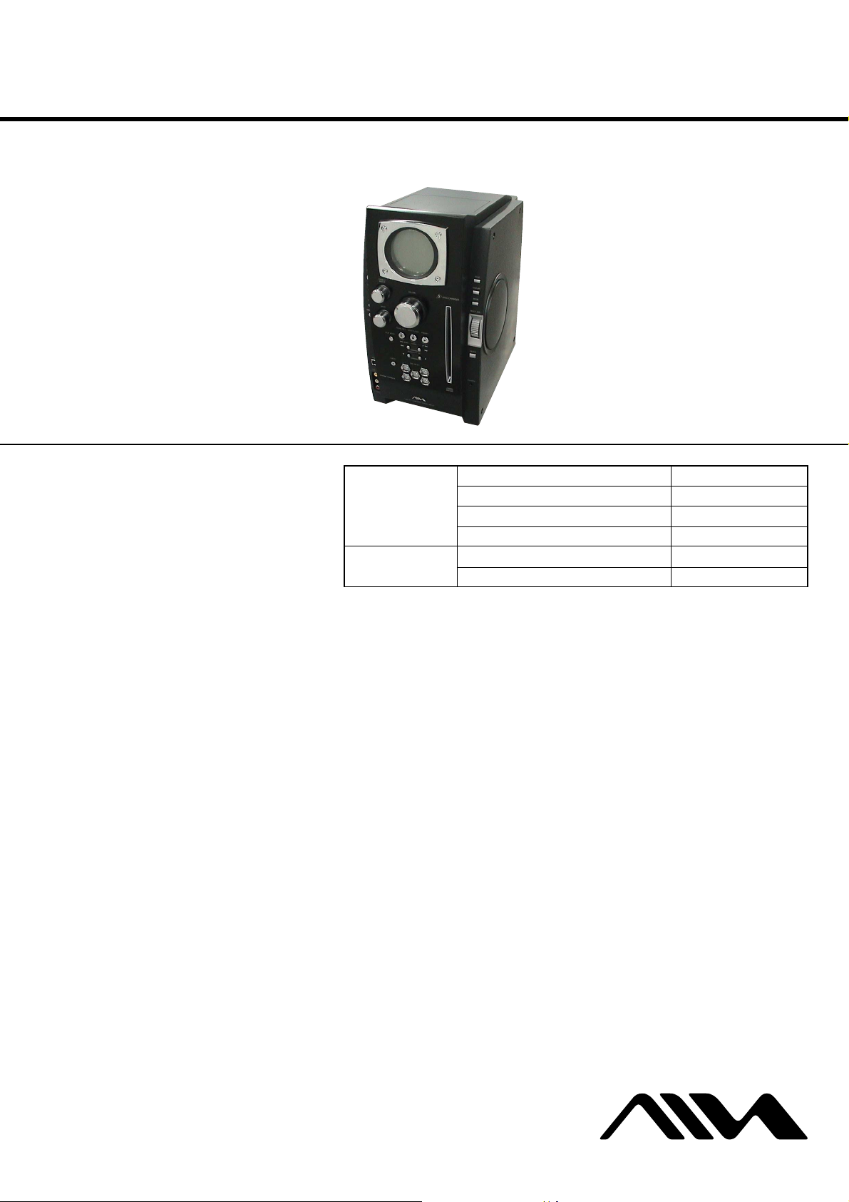
CX-BK1
SERVICE MANUAL
Ver 1.0 2003.06
• CX-BK1 is the amplifier, CD pla yer, tape dec k
and tuner section in BMZ-K1.
• Tape deck is not loaded in US model.
Licensed by BBE Sound, Inc. under USP4638258, 5510752
and 5736897.
CD Section
TAPE Section
(Except US model)
US Model
AEP Model
UK Model
E Model
Model Name Using Similar Mechanism NEW
CD Mechanism Type CDM69BV-30CBD64NS
Base Unit Name BU-30CBD64NS
Optical Pick-up Name A-MAX.3
Model Name Using Similar Mechanism NEW
Tape T ransport Mechanism T ype CMAL1Z240A
TUNER
FM tuning range 87.5 MHz to 108 MHz
FM usable sensitivity (IHF) 13.2 dBf
FM antenna terminal 75 Ω (unbalanced)
AM tuning range 530 kHz to 1710 kHz (10 kHz step)
531 kHz to 1710 kHz (9 kHz step)
AM usable sensitivity 350 µV/m
AM antenna Loop antenna
AMPLIFIER
Power output
US model: 110 W + 110 W (40 Hz - 20 kHz,
THD less than 1%, 6 Ω)
140 W + 140 W (40 Hz - 20 kHz,
THD 10%, 6 Ω)
Chilean, Peruvian and Mexican models:
140 W + 140 W (1 kHz, THD
less than 1%, 6 Ω)
180 W + 180 W (1 kHz, THD
10%, 6 Ω)
Total harmonic distortion 0.08 % (90 W, 1 kHz, 6 Ω)
Input LINE IN VIDEO: 1.0 Vp-p (75 Ω)
LINE IN AUDIO: 1.1 V
AUX (MD) IN: 1.1 V
MIC: 2.5mV (Chilean, Peruvian
and Mexican models)
Outputs SPEAKERS: 6 Ω or more
PHONES: 32 Ω or more
AUX (MD) OUT: 500 mV
VIDEO OUT: 1.0 Vp-p (75 Ω)
SPECIFICATIONS
CD PLAYER
Laser Semiconductor laser (λ = 800 nm)
Emission duration: continuous
D/A converter 1 bit dual
Signal-to-noise ratio 85 dB (1 kHz, 0 dB)
Wow and flutter Unmeasurable
CASSETTE DECK (Except US model)
Track format 4 tracks, 2 channels stereo
Frequency response 100 Hz – 10000 Hz (± 3dB)
Recording system AC bias
Heads Recording/playback × 1, erase × 1
GENERAL
Power requirements
US model: 120 V, 60 Hz
Mexican model: 127 V, 60 Hz
Chilean and Peruvian models:
120 V/220 – 230 V/240 V AC
(switchable), 50/60 Hz
COMPACT DISC RECEIVER
COMPACT DISC DECK RECEIVER
Power consumption
US model: 120 W
Chilean and Peruvian models:
Mexican model: 160 W
Power consumption in standby mode
US model: with ECO mode on: 0.25 W
Chilean and Mexican models:
Dimensions (w/h/d) Approx. 211 × 379 × 419 mm
Mass
US model: Approx. 8.6 kg (19 lbs)
Chilean and Peruvian models:
Specifications and external appearance are subject to change
without notice.
155 W
with ECO mode off: 20 W
with ECO mode on: 0.25 W
with ECO mode off: 28 W
3
(8
/8 × 15 ×16 5/8 in.)
Approx. 9.9 kg
US model
9-877-426-01 Sony Corporation
2003F05-1 Home Audio Company
C 2003.06 Published by Sony Engineering Corporation
AEP, UK, Chilean, Peruvian and Mexican models
Page 2
CX-BK1
r
Notes on chip component replacement
•Never reuse a disconnected chip component.
• Notice that the minus side of a tantalum capacitor may be damaged by heat.
Flexible Circuit Board Repairing
•Keep the temperature of the soldering iron around 270 ˚C during repairing.
• Do not touch the soldering iron on the same conductor of the
circuit board (within 3 times).
• Be careful not to apply force on the conductor when soldering
or unsoldering.
CAUTION
Use of controls or adjustments or performance of procedures
other than those specified herein may result in hazardous radiation exposure.
The following caution label is located inside the unit.
This appliance is classified
CLASS 1 LASER PRODUCT
LUOKAN 1 LASER LAITE
KLASS 1 LASER APPARAT
as a CLASS 1 LASER
product.
This label is located on the
rear exterior.
SAFETY CHECK-OUT
After correcting the original service problem, perform the following safety check before releasing the set to the customer:
Check the antenna terminals, metal trim, “metallized” knobs,
screws, and all other exposed metal parts for AC leakage.
Check leakage as described below.
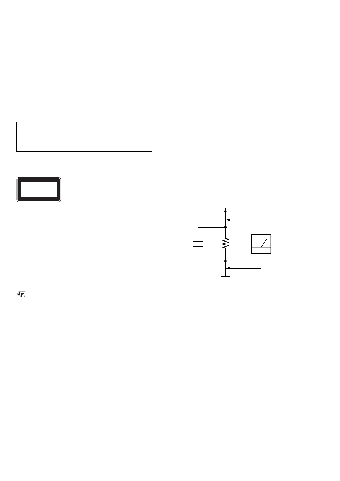
LEAKAGE TEST
The AC leakage from any exposed metal part to earth ground and
from all exposed metal parts to any exposed metal part having a
return to chassis, must not exceed 0.5 mA (500 microamperes.).
Leakage current can be measured by any one of three methods.
1. A commercial leakage tester, such as the Simpson 229 or RCA
WT -540A. Follo w the manufacturers’ instructions to use these
instruments.
2. A battery-operated AC milliammeter. The Data Precision 245
digital multimeter is suitable for this job.
3. Measuring the voltage drop across a resistor by means of a
VOM or battery-operated AC voltmeter. The “limit” indication is 0.75 V, so analog meters must have an accurate lowvoltage scale. The Simpson 250 and Sanwa SH-63Trd are examples of a passive VOM that is suitable. Nearly all battery
operated digital multimeters that have a 2 V A C range are suitable. (See Fig. A)
To Exposed Metal
Parts on Set
UNLEADED SOLDER
Boards requiring use of unleaded solder are printed with the leadfree mark (LF) indicating the solder contains no lead.
(Caution: Some printed circuit boards may not come printed with
the lead free mark due to their particular size)
: LEAD FREE MARK
Unleaded solder has the following characteristics.
• Unleaded solder melts at a temperature about 40 ˚C higher than
ordinary solder.
Ordinary soldering irons can be used but the iron tip has to be
applied to the solder joint for a slightly longer time.
Soldering irons using a temperature regulator should be set to
about 350 ˚C.
Caution: The printed pattern (copper foil) may peel away if the
heated tip is applied for too long, so be careful!
• Strong viscosity
Unleaded solder is more viscou-s (sticky, less prone to flow)
than ordinary solder so use caution not to let solder bridges occur such as on IC pins, etc.
• Usable with ordinary solder
It is best to use only unleaded solder but unleaded solder may
also be added to ordinary solder.
AC
1.5 k
0.15 µF
Fig. A. Using an AC voltmeter to check AC leakage.
Ω
Earth Ground
voltmete
(0.75 V)
SAFETY-RELATED COMPONENT WARNING!!
COMPONENTS IDENTIFIED BY MARK 0 OR DOTTED
LINE WITH MARK 0 ON THE SCHEMATIC DIA GRAMS
AND IN THE PARTS LIST ARE CRITICAL TO SAFE
OPERATION. REPLACE THESE COMPONENTS WITH
SONY PARTS WHOSE PART NUMBERS APPEAR AS
SHOWN IN THIS MANUAL OR IN SUPPLEMENTS PUBLISHED BY SONY.
2
Page 3

TABLE OF CONTENTS
CX-BK1
1. SERVICING NOTES ................................................ 4
2. GENERAL
Location of Controls ....................................................... 6
3. DISASSEMBLY
3-1. Disassembly Flow ........................................................... 8
3-2. Panel ................................................................................ 9
3-3. Top Panel Block .............................................................. 9
3-4. Fr ont Panel Assy ............................................................. 10
3-5. MAIN Board ................................................................... 10
3-6. Rear Cover....................................................................... 11
3-7. Tuner (FM/AM) .............................................................. 11
3-8. SPEAKER Board ............................................................ 12
3-9. ACDC Board, Power Transformer.................................. 12
3-10. AMP Board ..................................................................... 13
3-11. CD Mechanism Deck (CDM69BV-30CBD64NS)......... 13
3-12. Signal Cassette Mechanism ............................................ 14
3-13. Base Unit Section............................................................ 14
3-14. Base Unit (BU-30CBD64NS)......................................... 15
3-15. BD Board......................................................................... 15
3-16. SW (1) Board, SW (2) Board, SW (3) Board,
SW (4) Board, Bracket (Top) Assy................................. 16
3-17. CONNECTOR Board ..................................................... 16
3-18. Motor (Stocker) Assy (Stocker) (M761) ........................ 17
3-19. Motor (Roller) Assy (Roller) (M781)............................. 17
3-20. Motor (Mode) Assy (Mode) (M771) .............................. 18
3-21. Rubber Roller (Slider) Assy ........................................... 18
3-22. Timing Belt (Front/Rear) ................................................ 19
3-23. Cam (Gear)...................................................................... 19
3-24. SENSOR Board............................................................... 20
4. ASSEMBLY
4-1. How to Install the Cam (Eject Lock) .............................. 21
4-2. How to Install the Cam (Gear)........................................ 21
4-3. How to Install the Gear (Mode C) .................................. 22
4-4. How to Install the Gear (Mode Cam) ............................. 22
4-5. How to Install the Rotary Encoder (S702),
Gear (Stocker Communication) ...................................... 23
4-6. How to Install the Stocker Assy...................................... 23
5. TEST MODE.............................................................. 24
6. MECHANICAL ADJUSTMENTS....................... 25
7. ELECTRICAL ADJUSTMENTS
Deck Section ................................................................... 25
CD Section ...................................................................... 28
8. DIAGRAMS
8-1. Block Diagram – CD Section – ..................................... 31
8-2. Block Diagr am – TUNER/TAPE/USB Section – ......... 32
8-3. Block Diagr am – AMP Section – .................................. 33
8-4. Block Diagr am – POWER SUPPLY Section –............. 34
8-5. Note for Printed Wiring Boards
and Schematic Diagrams ................................................ 35
8-6. Printed Wiring Board – BD Board – ............................. 36
8-7. Schematic Diagram – BD Board – ................................ 37
8-8. Printed Wiring Boards – CHANGER Section –............ 38
8-9. Schematic Diagram – CHANGER Section – ................ 39
8-10. Printed Wiring Board
– DECK Board (Except US model) –............................ 40
8-11. Schematic Diagram
– DECK Board (Except US model) –............................. 41
8-12. Printed Wiring Board – MAIN Board – ........................ 43
8-13. Schematic Diagram – MAIN Board (1/4) – .................. 44
8-14. Schematic Diagram – MAIN Board (2/4) – .................. 45
8-15. Schematic Diagram – MAIN Board (3/4) – .................. 46
8-16. Schematic Diagram – MAIN Board (4/4) – .................. 47
8-17. Printed Wiring Board – USB AUX Board –.................. 48
8-18. Schematic Diagram – USB AUX Board –..................... 49
8-19. Printed Wiring Boars – MIC Board
(Chilean, Peruvian and Mexican models) – ................... 50
8-20. Schematic Diagram – MIC Board
(Chilean, Peruvian and Mexican models) – ................... 51
8-21. Schematic Diagram – AMP Board (1/2) – .................... 52
8-22. Schematic Diagram – AMP Board (2/2) – .................... 53
8-23. Printed Wiring Board – AMP Board – .......................... 54
8-24. Printed Wiring Board – HEADPHONE Board – .......... 55
8-25. Schematic Diagram – HEADPHONE Board – ............. 55
8-26. Printed Wiring Board – SPEAKER Board – ................. 56
8-27. Schematic Diagram – SPEAKER Board –.................... 57
8-28. Printed Wiring Boards – KEY Section –....................... 58
8-29. Schematic Diagram – KEY Section – ........................... 59
8-30. Printed Wiring Boards – LCD Section – ....................... 60
8-31. Schematic Diagram – LCD Section – ........................... 61
8-32. Printed Wiring Board – ACDC Board – ........................ 62
8-33. Schematic Diagram – ACDC Board – ........................... 63
8-34. Printed Wiring Board
– PT Board (US, AEP and UK models) – ...................... 64
8-35. Schematic Diagram
– PT Board (US, AEP and UK models) – ...................... 65
8-36. Printed Wiring Board – PT Board
(Chilean, Peruvian and Mexican models) – ................... 66
8-37. Schematic Diagram – PT Board
(Chilean, Peruvian and Mexican models) – ................... 67
8-38. IC Pin Function Description ........................................... 73
9. EXPLODED VIEWS
9-1. Panel Section ................................................................... 79
9-2. Top Panel Block .............................................................. 80
9-3. F ront Panel Block-1 ........................................................ 81
9-4. F ront Panel Block-2 ........................................................ 82
9-5. F ront Panel Block-3 ........................................................ 83
9-6. Chassis Block-1............................................................... 84
9-7. Chassis Block-2............................................................... 85
9-8. CD Mechanism Deck Section-1
(CDM69BV-30CBD64NS) ............................................. 86
9-9. CD Mechanism Deck Section-2
(CDM69BV-30CBD64NS) ............................................. 87
9-10. CD Mechanism Deck Section-3
(CDM69BV-30CBD64NS) ............................................. 88
9-11. CD Mechanism Deck Section-4
(CDM69BV-30CBD64NS) ............................................. 89
9-12. CD Mechanism Deck Section-5
(CDM69BV-30CBD64NS) ............................................. 90
9-13. CD Mechanism Deck Section-6
(CDM69BV-30CBD64NS) ............................................. 91
9-14. Optical Pick-up Section (BU-30CBD64NS).................. 92
10. ELECTRICAL PARTS LIST ............................... 93
3
Page 4
CX-BK1
SECTION 1
SERVICING NOTES
NOTES ON HANDLING THE OPTICAL PICK-UP
BLOCK OR BASE UNIT
The laser diode in the optical pick-up block may suffer electrostatic break-down because of the potential difference generated
by the charged electrostatic load, etc. on clothing and the human
body.
During repair, pay attention to electrostatic break-down and also
use the procedure in the printed matter which is included in the
repair parts.
The flexible board is easily damaged and should be handled with
care.
NOTES ON LASER DIODE EMISSION CHECK
The laser beam on this model is concentrated so as to be focused
on the disc reflective surface by the objective lens in the optical
pick-up block. Therefore, when checking the laser diode emission, observe from more than 30 cm away from the objectiv e lens.
LASER DIODE AND FOCUS SEARCH OPERATION
CHECK
Carry out the “S curve check” in “CD section adjustment” and
check that the S curve waveforms is output three times.
• MODEL IDENTIFICATION
– Rear Cover –
PART No.
MODEL PART No.
US model 4-245-039-0
Chilean and Peruvian models 4-245-039-1
AEP and UK models 4-245-039-2
Mexican model 4-245-039-3
[]
[]
[]
[]
SERVICE POSITION
– Tape mechanism deck (except US) –
Connect the wire (flat type) (8 core)
to the main board (CN903) and
the mechanism deck.
Connect the wire (flat type) (11 core)
to the deck board (CN008) and the main board (CN009).
4
Page 5
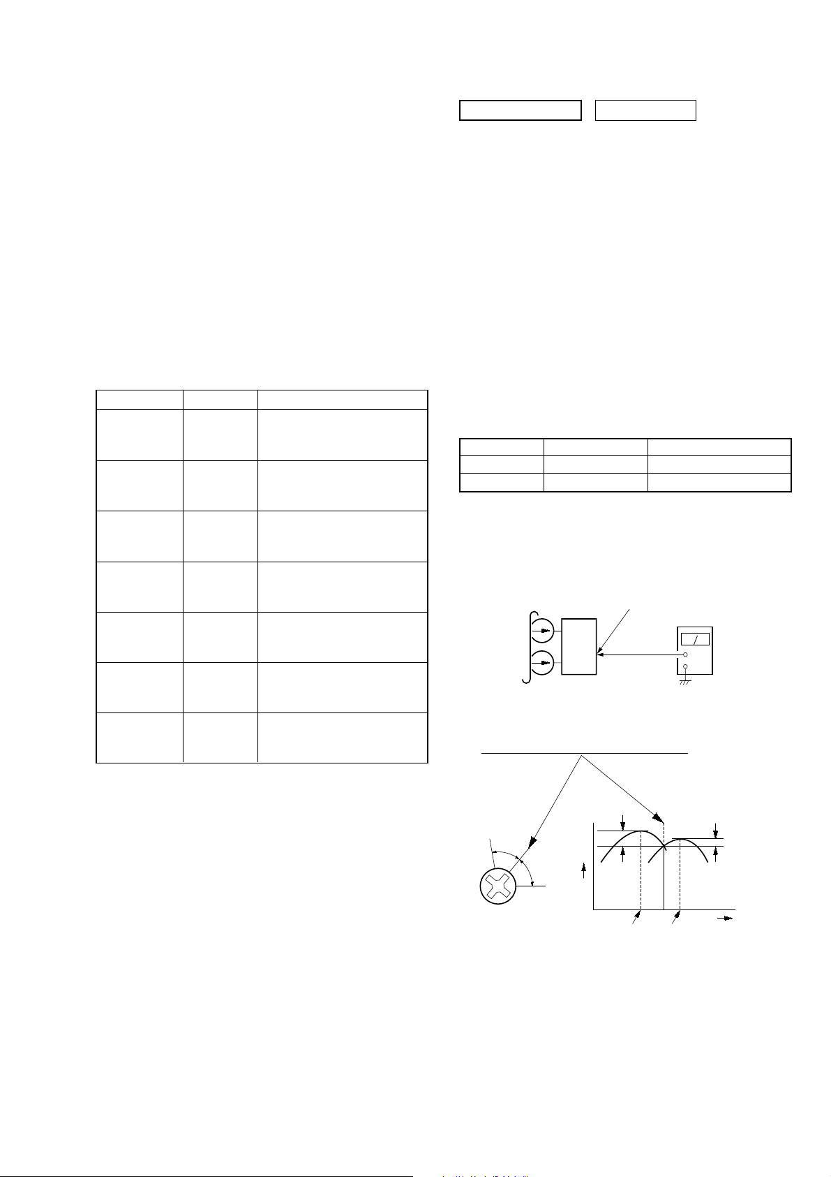
– CD mechanism deck –
• In checking the CD mechanism deck section, prepare three extension jigs (Part No. J-2501-242-A:1.00 mm 11core/
Part No. J-2501-245-A: 1.00 mm 23 core/Part No. J-2501-248-A: 1.00mm 27 core).
Note: The CD mechanism deck of this model is a vertical type and putting it vertically as shown in the figure is the standard position.
When checking signals such as RF waveforms, operate it with the CD mechanism deck in the standard position as shown below.
Connect the extension jig (J-2501-248-A)
to the connector board (CN701) and
the main board (CN901).
CX-BK1
Connect the extension jig (J-2501-245-A)
to the BD board (CN102) and
the main board (CN902).
Connect the extension jig (J-2501-242-A)
to the BD board (CN104) and the main board (CN507).
– main board, ACDC board –
• For connecting the CD mechanism deck, prepare three extension jigs. (Refer to “– CD mechanism deck –”)
AMP board
speaker board
PT board
front panel section
ACDC board
main board
tuner unit
CD mechanism deck
5
Page 6
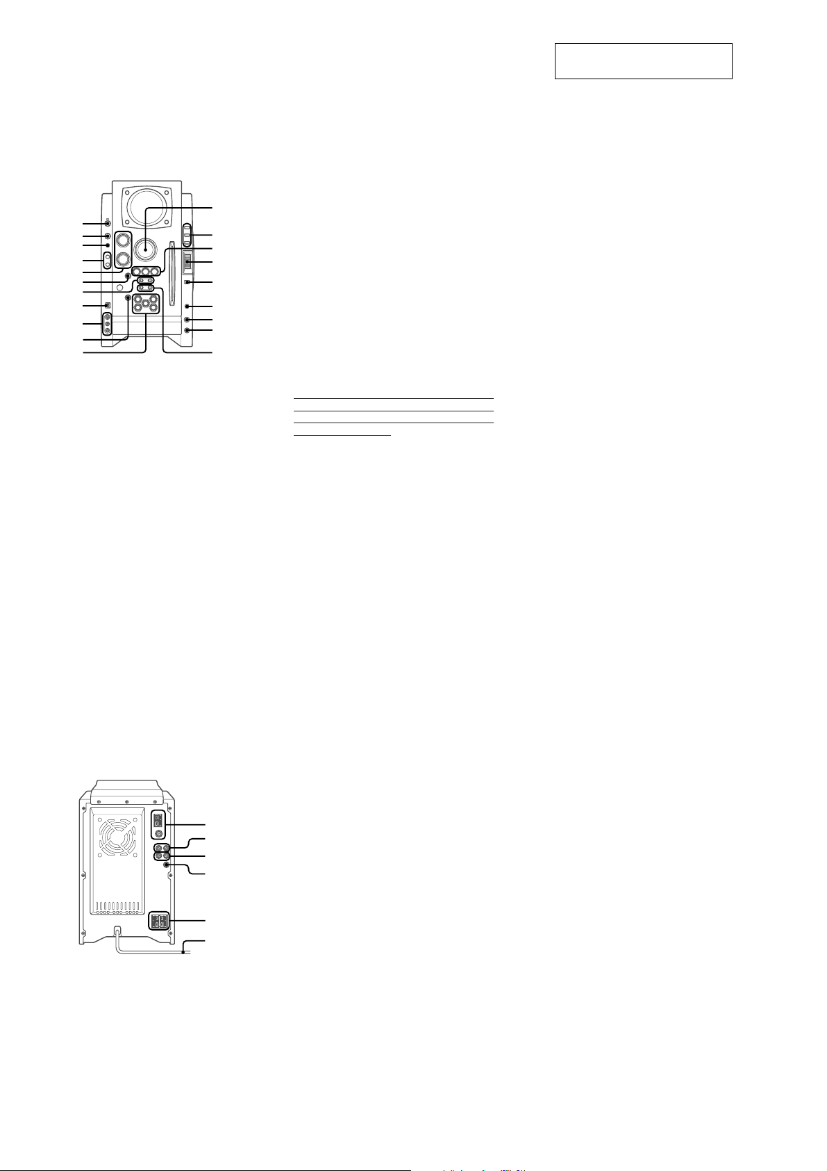
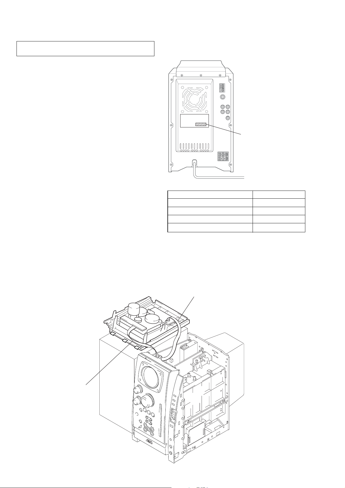
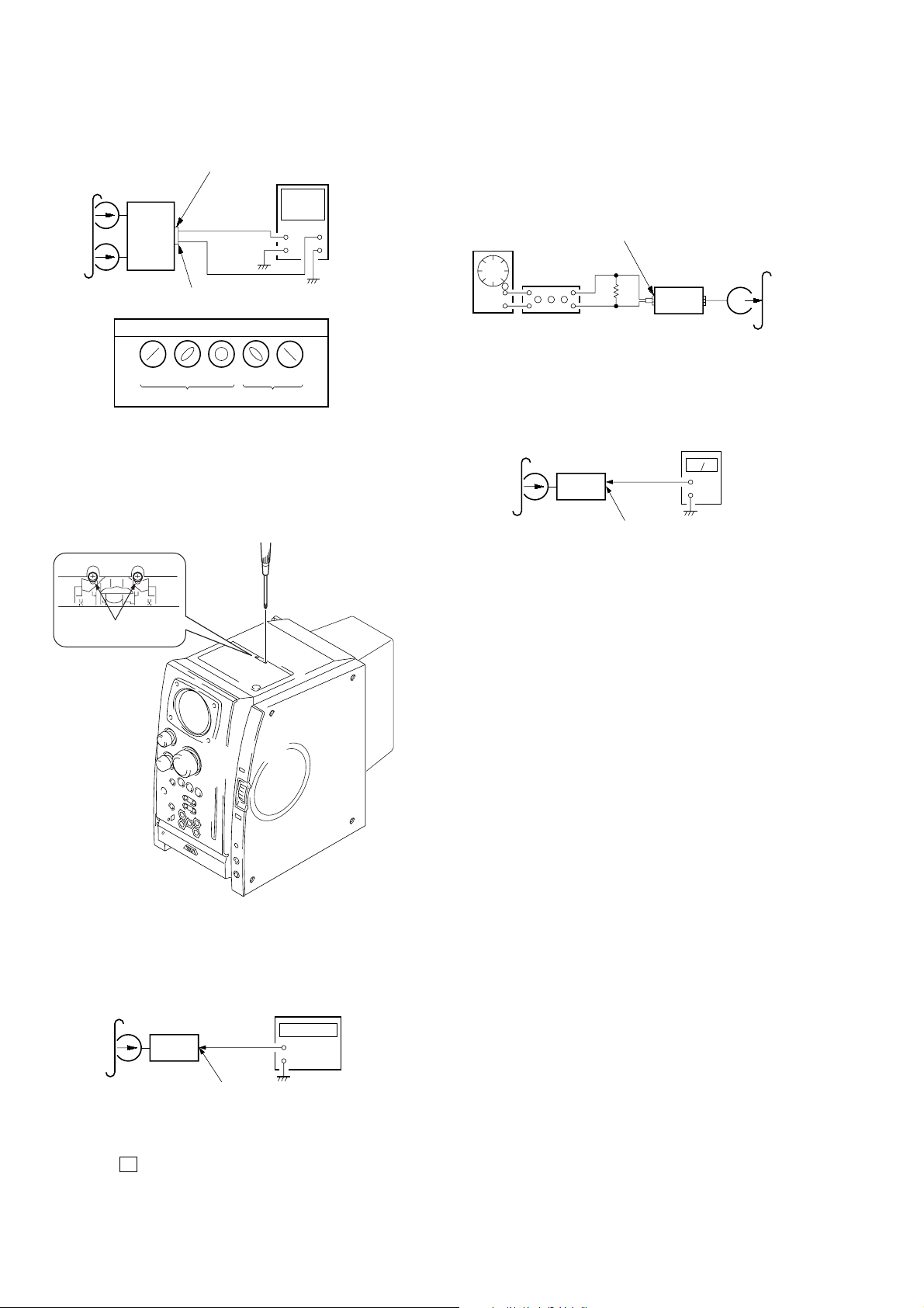
CX-BK1
• LOCATION OF CONTROLS
SECTION 2
GENERAL
This section is extracted from
instruction manual.
Main unit: front
1
2
3
4
5
6
7
8
9
0
!
1 POWER 6STANDBY/ON
Switches the unit on and off (standby).
2 FUNCTION
Switches the active function among CD, USB, TAPE
(Except US model), TUNER, VIDEO and AUX.
3 BAND
Select tuner function and the tuner band.
4 GEQ
Selects a sound equalization curve.
i-Bass
Produces rich and clear low frequency sound.
5 TREBLE/MIDDLE
Adjusts the treble or middle range level.
BASS
Adjusts the bass level.
6 PLA Y MODE (US model)
Selects various CD play mode.
wREC (Except US model)
Starts tape recording.
Also used to enter 4-second blank spaces during
@
#
$
%
^
&
*
(
)
recording.
7 TUNING DOWNf/r, UPg/t
CD: skips to a previous or a succeeding track when
pressed, searches a track in fast forward or reverse
playback when held down.
Tape: rewinds or fast forwards the tape. (Except US
model)
Tuner: manually tunes up or down within the band.
8 USB terminal
Accepts sound signals from a personal computer.
Connect your personal computer to this terminal with a
USB cable so that the unit can output the sound of an
audio file which is played back by the Winamp3 on your
computer.
Be sure to see “CONNECTING A PERSONAL
COMPUTER” for the details about the computer
requirements, how to connect and so on before actually
connecting your computer.
9 LINE IN (VIDEO/AUDIO) jacks
Accepts analog signals from external equipment.
Connect using an optional connecting cable with RCA
phono plugs (red plug to R jack, white plug to L jack,
yellow plug to VIDEO jack).
Refer also to the operating instructions of your equipment.
To switch function to external input, press FUNCTION
repeatedly to display “VIDEO”.
0 zEJECT
Ejects the disc(s).
! DISC SELECT (1-5)
Selects a disc slot.
Starts CD play for one desired disc.
@ VOLUME
Adjusts the volume.
#
TITLE
When the unit is turned off: activates or deactivated
DEMO.
Changes the display in MP3-CD or USB source.
DISPLAY
Changes the display in CD playback mode.
Turns the back light on and off when the unit is turned
off.
MODE
Selects various modes (sound adjustment, etc.) when
used in combination with ENTER and MULTI JOG.
Switches the ECO mode on and off when the unit is turned
off.
$ aPAUSE/SET
Pauses CD play.
sSTOP/CLEAR
Stops CD play.
cPRESET (US model)
Starts CD play.
dPRESET (Except US model)
Starts CD or tape play.
% MULTI JOG
When used in combination with ENTER and MULTI JOG,
CD: selects a track.
Tuner: selects a preset station.
^ ENTER
Fixes the modes and the time (clock and timer, etc.) when
used in combination with ENTER and MULTI JOG.
& PHONES jack
Plug in optional headphones set with a stereo mini plug
(Ø3.5 mm). Speaker output is canceled.
* MIC MIXING (Chilean and Peruvian
models)
Adjusts the microphone volume.
( MIC jack (Chilean and Peruvian models)
Connects the microphone.
) ALBUM/PLAY LIST k,i
Skips to a previous or succeeding album or play list.
Main unit: rear
1 AM LOOP jack and FM 75 Ω terminal
Plug in the supplied AM and FM antennas.
2 AUX IN jacks
Accept analogue sound signals from external equipment.
Connect external equipment using an optional connecting
cable with RCA phono plugs (red plug to R jack, white
1
2
3
4
5
6
plug to L jack). Refer also to the operating instructions
for your equipment.
To switch function to external input, press FUNCTION
repeatedly to display “AUX” (US model) or “MD”
(Chilean, Peruvian and Mexican models).
3 AUX OUT jacks
Analog sound signals for all functions can be output
through these jacks. Use a cable with RCA phono plugs
to connect audio equipment.
Connect the red plug to the R jack, and the white plug to
the L jack.
However, the signal is not output when the function is
“VIDEO” or “AUX” (US model) or “MD” (Chilean,
Peruvian and Mexican models).
4 VIDEO OUT
Signals from VIDEO IN jack output through this jack.
5 #SPEAKERS terminals
Connect the speaker cords of the supplied speakers.
6 AC power cord
6
Page 7

CX-BK1
Remote commander
Refer to the pages indicated in parentheses for details.
1
4
6
7
9
8
0
!
@
5
3
2
Buttons with the same or similar names on the main unit
basically have the same function.
1 POWER
2 1-9, 0/10, +10
CD: selects a track of the specified number.
Tuner: tunes in the station with the specified preset
number.
The numbered buttons take on these functions when
pressed with SHIFT held down.
3 c/d
Starts CD play.
s
a
f/g
r/ tPRESET
Tuner: selects a preset station.
M/ N ALBUM
Selects a previous or a succeeding album.
4 PLAY MODE
REPEAT
Selects repeat CD playback mode.
5 CLOCK/TIMER SET
Enters clock and timer setting mode.
CLOCK/TIMER SELECT
Switches timer setting on and off.
6 DISPLAY
SOUND
Selects bass, treble or middle range level setting mode.
CLEAR
Clears a track of the CD programed playback and a tuner
preset station.
7 SHIFT
Hold down when pressing a numbered button to change
its function to that printed above the number.
8 FUNCTION
9 DISC SKIP
Changes a disc slot.
0 ENTER
! SLEEP
Selects sleep-timer mode.
@ VOLUME +, -
EDIT (Chilean, Peruvian and Mexican
BAND
SPECTRUM
Changes the spectrum analyser display.
TUNER MODE
Switches between stereo or monaural FM reception.
models)
Selects edited CD recording.
KARAOKE (Chilean, Peruvian and
GEQ
Mexican models)
Selects a Karaoke mode.
Setting the clock
1
Press CLOCK/TIMER SET on the remote.
See below when to adjust the clock.
2
Press r or t to set the hour, then press
ENTER.
3
Press r or t to set the minute.
Each press changes the time in 1-minute steps.
4
Press ENTER.
The time display stops flashing and the clock starts from
00 seconds.
•MULTI JOG is also available in place of r or t.
To adjust the clock
1 Press CLOCK/TIMER SET on the remote.
2 Press r or t repeatedly to display “CLOCK” and
then press ENTER.
3 Carry out steps 2 to 4 described in “Setting the clock” to set
the time.
To display the time while the power is on
Press DISPLAY repeatedly. The clock display appears in the
display for 6 seconds.
If “- -:- -” appears when the unit is turned off
There has been a power interruption. Reset the clock.
7
Page 8
CX-BK1
• This set can be disassembled in the order shown below.
3-1. DISASSEMBLY FLOW
SECTION 3
DISASSEMBLY
SET
3-2. PANEL
(Page 9)
3-3. TOP PANEL BLOCK
(Page 9)
3-4. FRONT PANEL
ASSY
(Page 10)
3-5. MAIN BOARD
(Page 110)
3-7. TUNER (FM/AM)
(Page 11)
3-9. ACDC BOARD, POWER TRANSFORMER
(Page 12)
3-6. REAR COVER
3-8. SPEAKER BOARD
Note 1: The process described in can be performed in any order.
Note 2: Without completing the process described in , the next process can not be performed.
Note 3: Tape deck is not loaded in US model.
(Page 11)
(Page 12)
3-7. TUNER (FM/AM)
(Page 11)
3-8. SPEAKER
BOARD
(Page 12)
3-12. SIGNAL
CASSETTE
MECHANISM
(Page 14)
3-10. AMP BOARD
(Page 13)
3-11. CD MECHANISM DECK
(CDM69BV-30CBD64NS)
(Page 13)
3-13. BASE UNIT SECTION
(Page 14)
3-14. BASE UNIT
(BU-30CBD64NS)
(Page 15)
3-15. BD BOARD
(Page 15)
3-16. SW (1) BOARD,
SW (2) BOARD,
SW (3) BOARD,
SW (4) BOARD,
BRACKET (TOP) ASSY
(Page 16)
3-19. MOTOR (ROLLER)
ASSY (ROLLER)
(M781)
(Page 17)
3-18. MOTOR (STOCKER)
ASSY (STOCKER)
(M761)
(Page 17)
3-21. RUBBER ROLLER
(SLIDER) ASSY
(Page 18)
3-22. TIMING BELT
(FRONT/REAR)
(Page 19)
3-17. CONNECTOR BOARD
(Page 16)
3-20. MOTOR (MODE)
ASSY (MODE)
(M771)
(Page 18)
3-23. CAM (GEAR)
(Page 19)
3-24. SENSOR BOARD
(Page 20)
8
Page 9
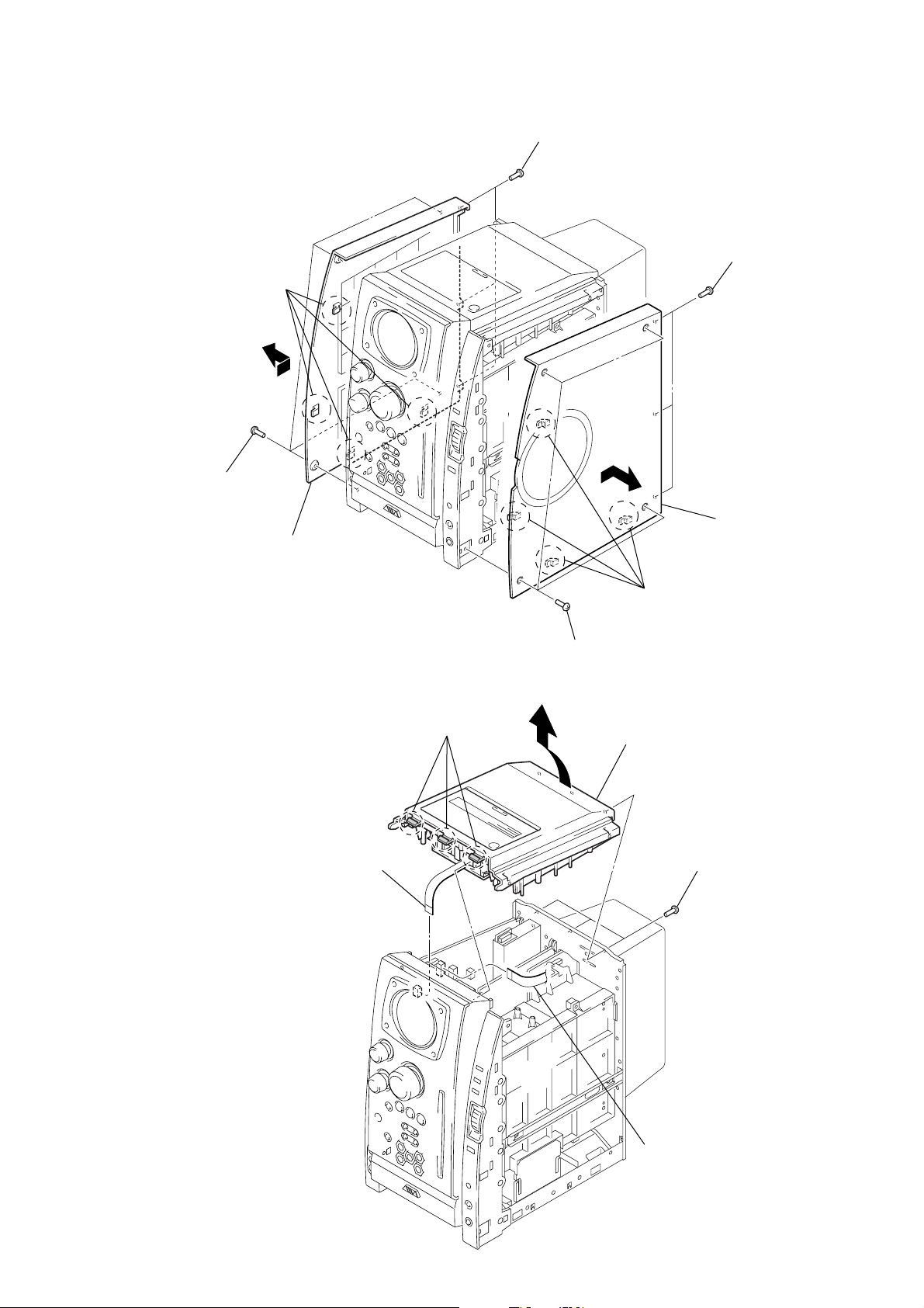
Note: Follow the disassembly procedure in the numerical order given.
)
3-2. PANEL
•
Tape deck is not loaded in US model.
The shape of the top panel shown in
“DISASSEMBLY” is different from the
actual shape.
3
four claws
4
2
four screws
(BVTP3
×
10)
1
three screws
(BVTP3
×
10)
9
6
three screws
(BVTP3
0
right panel
CX-BK1
×
10)
5
panel (left)
3-3. TOP PANEL BLOCK
•
Tape deck is not loaded in US model.
The shape of the top panel shown
in “DISASSEMBLY” is different from
the actual shape.
4
wire (flat type) (8core)
(CN903)
2
three claws
7
3
four screws
(BVTP3
×
top panel block
6
8
10)
four claws
1
three screws
(BVTP3
×
10)
5
wire (flat type) (11core
(CN009)
9
Page 10
CX-BK1
)
3-4. FRONT PANEL ASSY
9
1
wire (flat type) (19core)
(CN905)
front panel assy
2
wire (flat type) (17core)
(CN004)
E51, MX
3
wire (flat type) (5core)
(CN504)
6
3-5. MAIN BOARD
2
wire (flat type)
(11core: US, E51) (CN509)/
(15core: AEP, UK) (CN508)
qs
two screws
(BVTP3 × 10)
main board
5
five screws
(BVTP3 × 10)
5
1
wire (flat type) (11core)
(CN502)
6
wire (flat type) (11core)
(CN507)
8
7
six screws
(BVTP3 × 10)
7
8
two claws
connector
(CN007)
connector
(CN006)
4
connector (CN530)
3
two screws
(BVTP3
×
4
10)
screw
(BVTP3
×
10
10
qa
two screws
(BVTP3
0
×
6)
wire (flat type) (27core)
(CN901)
9
wire (flat type) (23core)
(CN902)
Page 11
3-6. REAR COVER
)
r
3
connector
(CN303)
2
1
seven screws
(BVTP3
rear cove
4
CX-BK1
×
10
3-7. TUNER (FM/AM)
2
tuner (FM/AM)
1
two screws
(BVTP3
×
8)
11
Page 12
CX-BK1
)
3-8. SPEAKER BOARD
3
speaker board
2
two screws
(BVTP3
×
10
1
connector
(CN503)
3-9. ACDC BOARD, POWER TRANSFORMER
1
connector (CN003)
2
connector (CN006)
5
seven screws
(BVTP3 × 10)
3
connector (CN011)
7
connector
(E51, MX: CN015)/
(US: CN011)/
(AEP, UK: CN001)
4
two screws
(BVTP3 × 10)
6
ACDC board
12
9
two screws
(ITC+4-8)
0
power transformer
8
connector
(CN008)
8
connector
(CN010)
EXCEPT E51
E51
Page 13

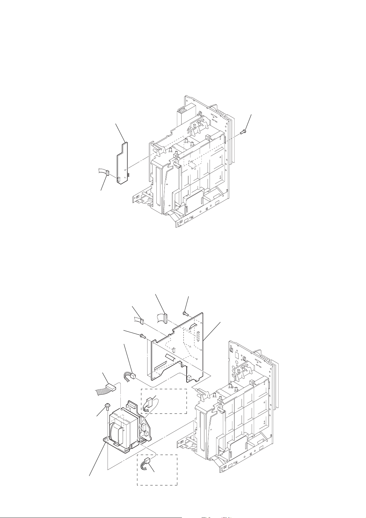
3-10. AMP BOARD
)
4
two screws
(BVTP3
×
10)
5
AMP board
3
two screws
(BVTP3
×
CX-BK1
10)
1
3-11. CD MECHANISM DECK (CDM69BV-30CBD64NS)
5
disk mecanical holder
4
four screws
(BVTP3 × 10)
2
CD support board
two screws
(BVTP3
×
10)
1
four screws
(BVTP3 × 10
6
CD mechanism deck (CDM69BV-30CBD64NS)
3
disk mechanical cover
2
four screws
(BVTP3 × 10)
13
Page 14
CX-BK1
3-12. SIGNAL CASSETTE MECHANISM
•
Tape deck is not loaded in US model.
1
connector
(CN302)
3
signal cassette mechanism
2
3-13. BASE UNIT SECTION
four screws
(BVTP3 × 10)
2
screw
(+PTPWH) (M2) (DIA. 7)
14
4
boss
7
base unit section
5
boss
6
boss
3
boss
1
floating
screw
(DIA. 12)
Page 15
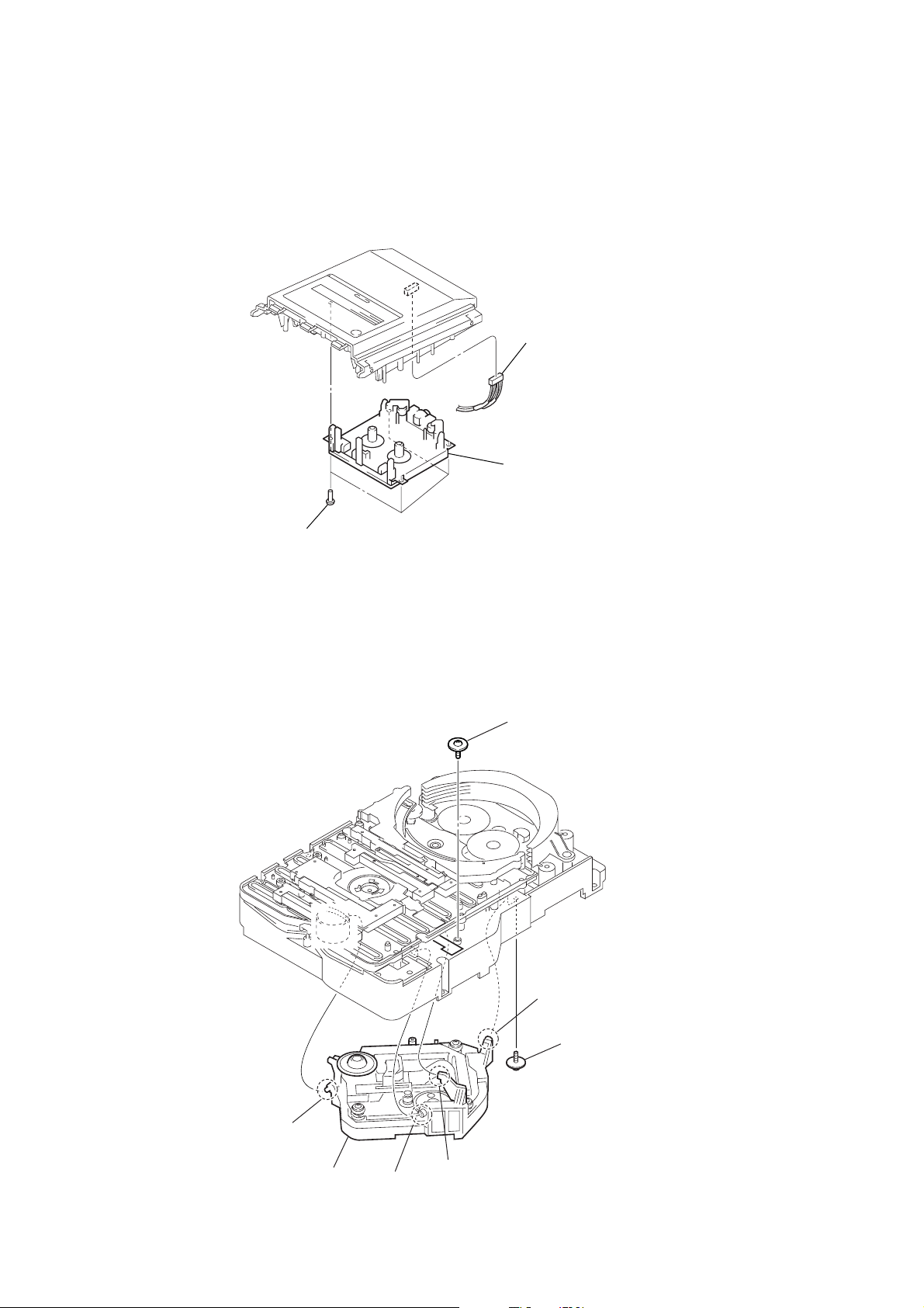
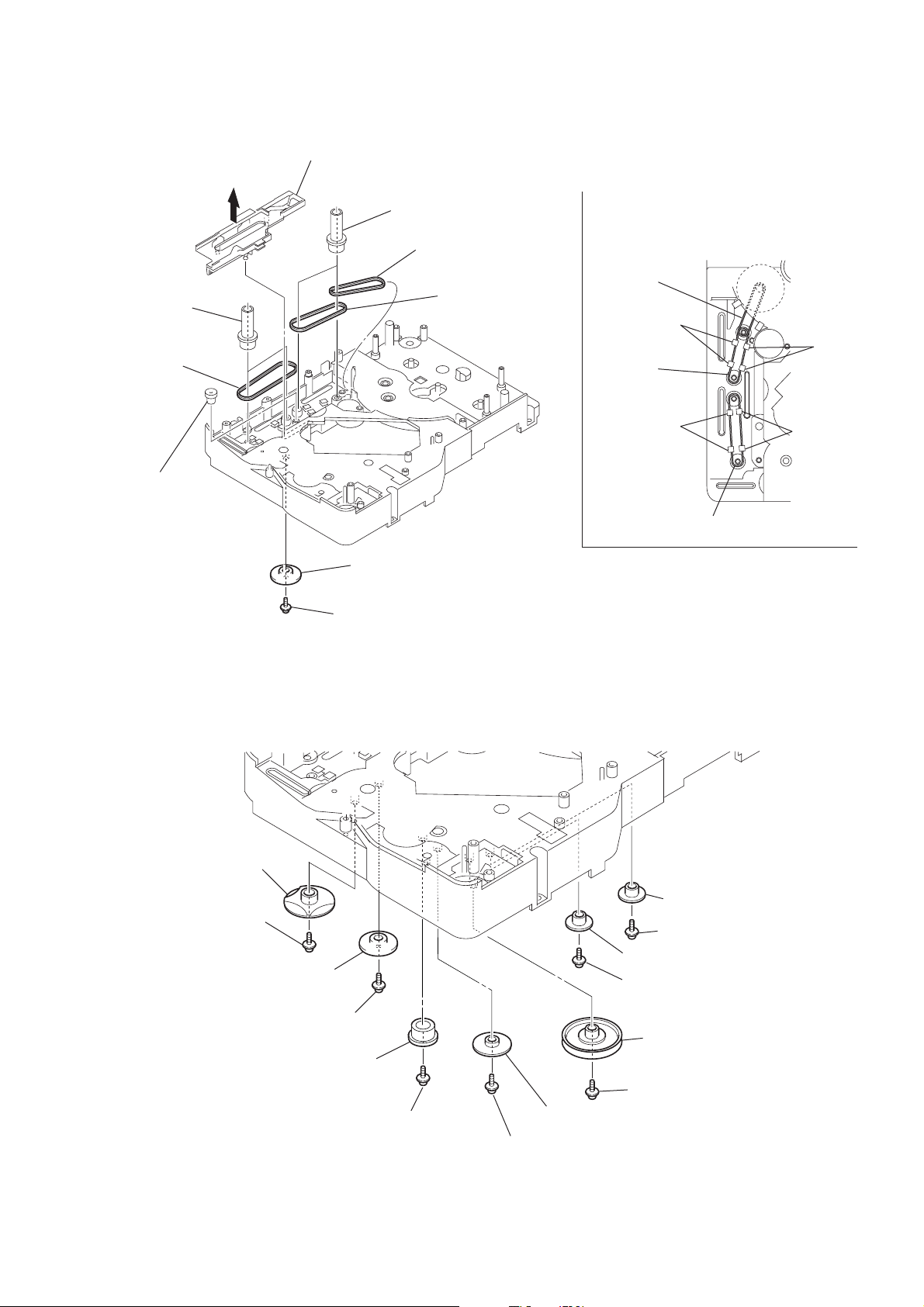
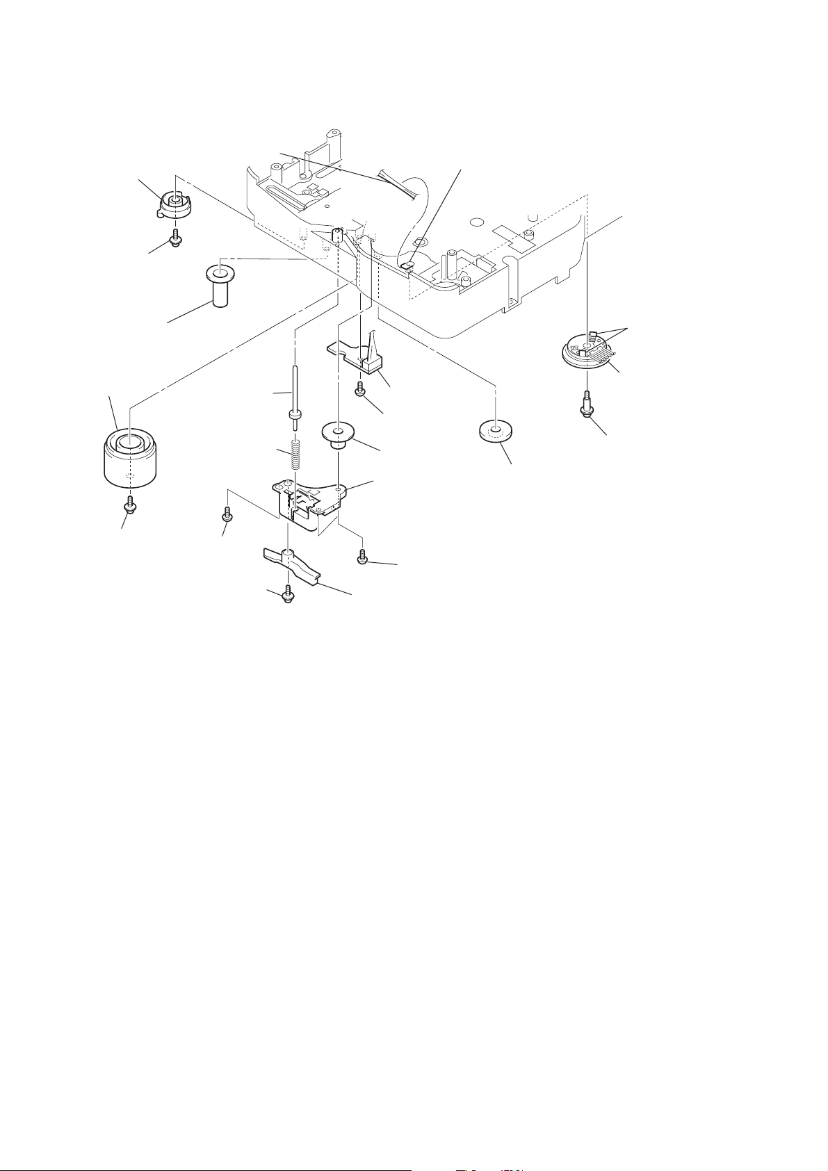
3-14. BASE UNIT (BU-30CBD64NS)
r
qa
base unit (BU-30CBD64NS)
1
tension spring (BU30-1)
5
floating screw
(+PTPWHM2.6
q;
vibration proof rubbers
×
6)
6
4
floating screw
(+PTPWHM2.6
9
vibration proof rubber
2
floating screw
(+PTPWHM2.6
7
vibration proof rubber
×
6)
3
floating screw
(+PTPWHM2.6
8
vibration proof rubber
×
6)
CX-BK1
×
6)
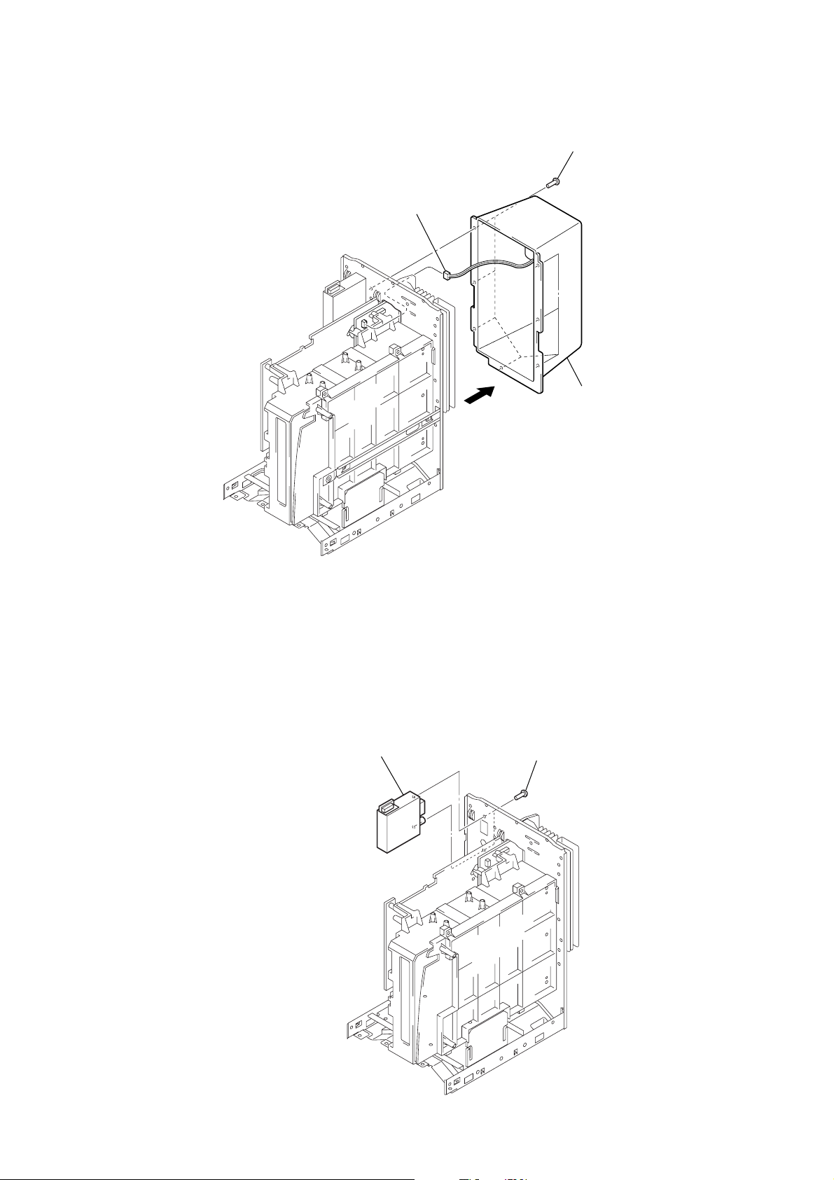
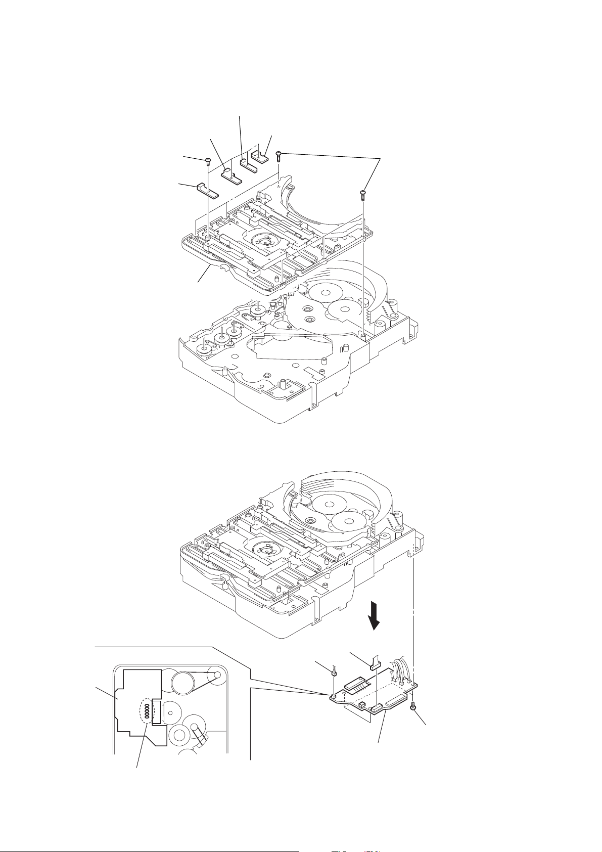
3-15. BD BOARD
2
wire (flat type) (11 core)
5
BD board
4
wire (flat type) (16 core)
3
Remove the solde
(four portions).
1
wire (flat type) (23 core)
15
Page 16
CX-BK1
)
)
3-16. SW (1) BOARD, SW (2) BOARD, SW (3) BOARD, SW (4) BOARD, BRACKET (TOP) ASSY
4
SW (3) board
5
SW (4) board
6
six screws
(BVTP2.6
×
8
1
four
(BTP2.6
2
SW (1) board
7
3
SW (2) board
screws
×
6)
bracket (top) assy
3-17. CONNECTOR BOARD
– bottom view –
CONNECTOR board
5
connector
(CN703)
4
connector
(CN710)
3
2
four screws
6
CONNECTOR board
(BVTP2.6
×
8
16
1
Remove five solders.
Page 17
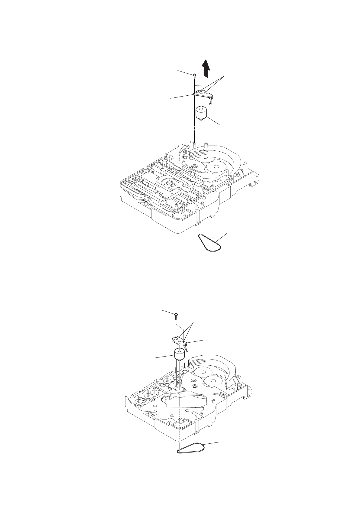
3-18. MOTOR (STOCKER) ASSY (STOCKER) (M761)
s
d
CX-BK1
3
two screws
(BVTP2.6
5
stocker motor board
×
4
8)
2
Remove two solder
6
motor (stocker) assy (stocker) (M761)
1
belt (stocker)
3-19. MOTOR (ROLLER) ASSY (ROLLER) (M781)
3
two screws
5
motor (roller) assy
(roller)(M781)
2
Remove two solders.
4
ROLLER MOTOR
1
boar
belt (roller V)
17
Page 18
CX-BK1
)
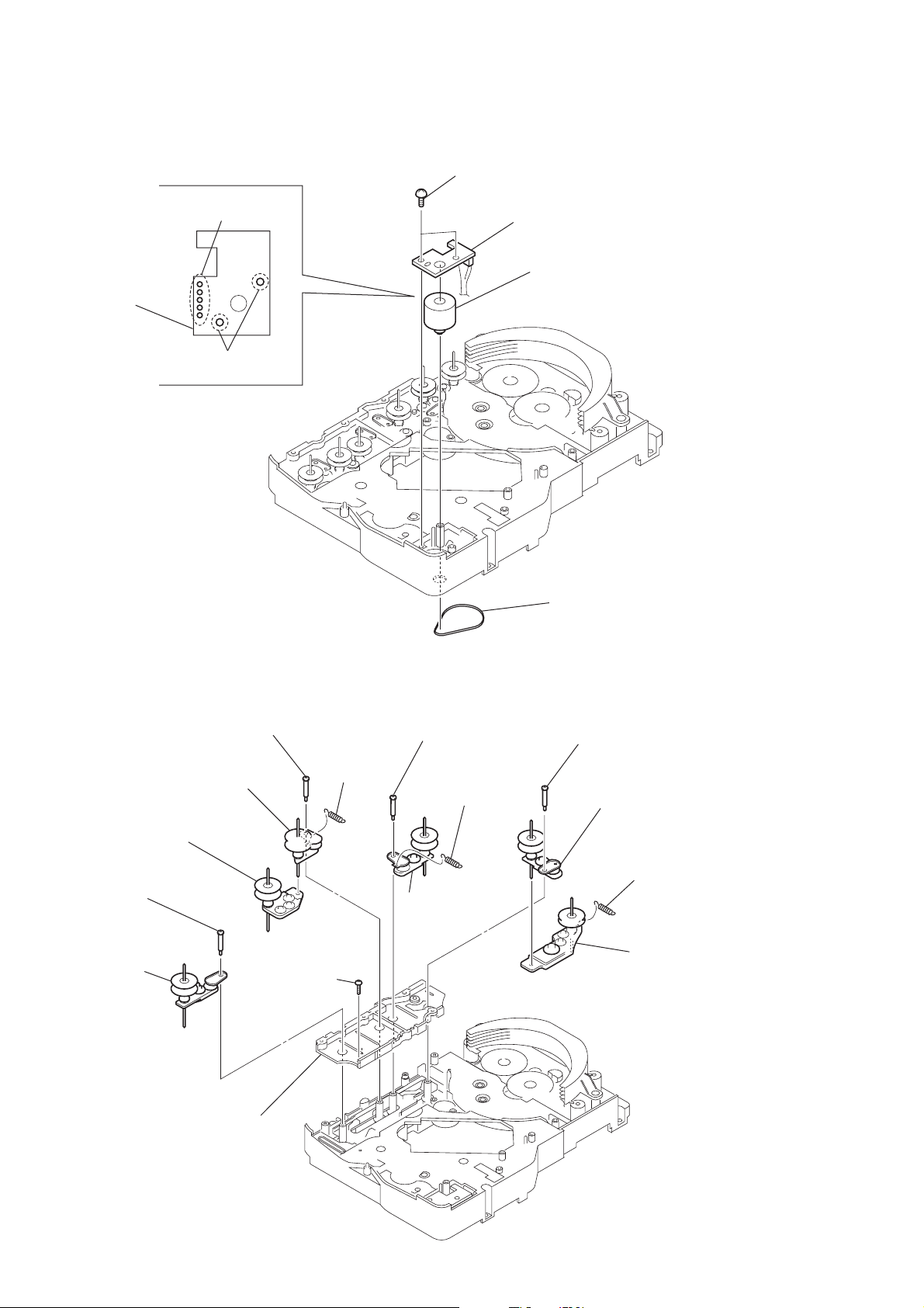
3-20. MOTOR (MODE) ASSY (MODE) (M771)
1
Remove five solders
of rotary encoder.
MODE MOTOR
board
2
Remove two solders
of motor (M771)
3
two screws
(BVTP2.6
×
8)
4
MODE MOTOR board
6
motor (mode) assy (mode) (M771)
3-21. RUBBER ROLLER (SLIDER) ASSY
8
qs
qd
rubber roller
(slider 1) assy
qa
rubber roller
(slider 2) assy
step screw
0
rubber roller
(slider 4) assy
step screw
qf
screw
(BVTP2.6
9
×
tension
spring
(slider 2)
8)
5
step screw
6
tension spring
(base slider 4)
7
rubber roller
(slider 1) assy
5
belt (mode V)
1
step screw
2
rubber roller
(slider S) assy
3
4
tension spring
(base slider 5
rubber roller
(slider 5) assy
18
qg
sub chassis
Page 19
3-22. TIMING BELT (FRONT/REAR)
)
3
slider (mode cam) assy
5
two gears
(center)
6
timing belt
(front)
7
two gears (center)
8
timing belt (rear)
9
timing belt (rear)
When install three timing belts,
its pass under each claws.
timing belt
(rear)
claw
timing belt
(rear)
CX-BK1
claw
4
gear
(timing)
3-23. CAM (GEAR)
qf
cam (gear)
: Note
2
gear (mode cam)
: Note
1
screw
(PTPWH2.6
×
claw
timing belt (front)
Note: Refer to assembly (Section 4)
8)
claw
qd
screw
qs
gear(mode cam)
qa
screw
(PTPWH2.6
0
Note: Refer to assembly
(Section 4).
×
8)
gear (mode C)
:Note
9
screw
(PTPWH2.6
6
gear (mode 5)
5
screw (PTPWH2.6 × 8
4
gear (mode 5)
3
screw (PTPWH2.6 × 8)
2
pulley
(mode deceleration)
1
screw(PTPWH2.6 × 8)
8
gear (mode D)
×
8)
7
screw (PTPWH2.6 × 8)
19
Page 20
CX-BK1
r
3-24. SENSOR BOARD
q;
cam (eject lock)
: Note
9
screw
(PTPWH2.6
qs
cam (BU U/D)
qd
×
8)
gear (eject lock)
7
compression spring
(shutter)
ql
8
harness
shaft
(shutter)
wa
SENSOR board
w;
screw
(BVTP2.6
6
gear (mode A)
5
base (shutter) block
qk
claw
qh
two claws
qj
rotary encode
(S771)
×
8)
qf
gear
(mode B)
qg
screw
(PTPWH2.6
×
8)
qa
screw
(PTPWH2.6
3
8)
screw
(BVTP2.6
1
screw
(PTPWH2.6
×
8)
4
two screws
×
8)
2
lever shutter (A)
(BVTP2.6
×
8)
Note: Refer to assembly (Section 4).
×
20
Page 21
SECTION 4
ASSEMBLY
• This set can be assembled in the order shown below.
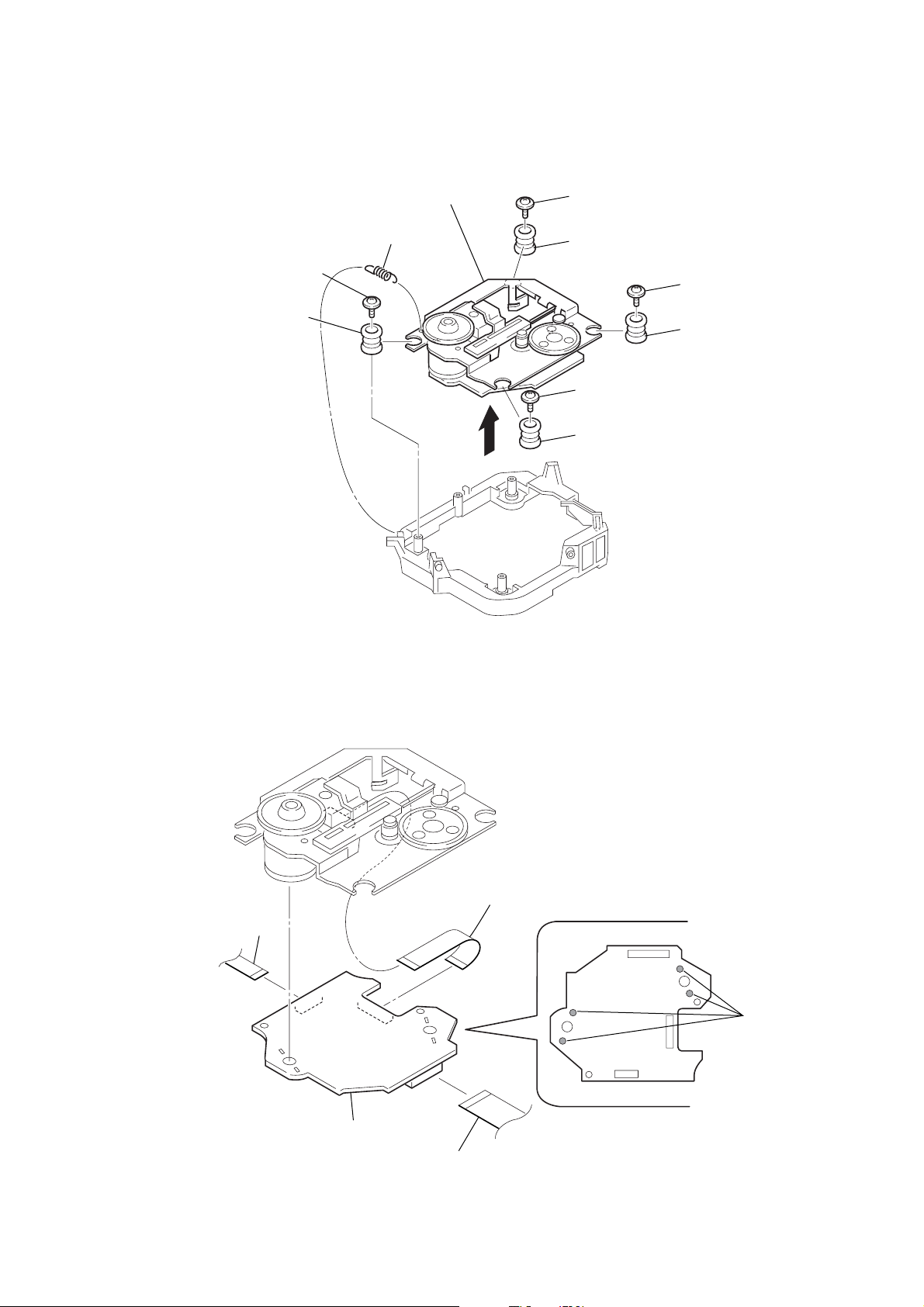
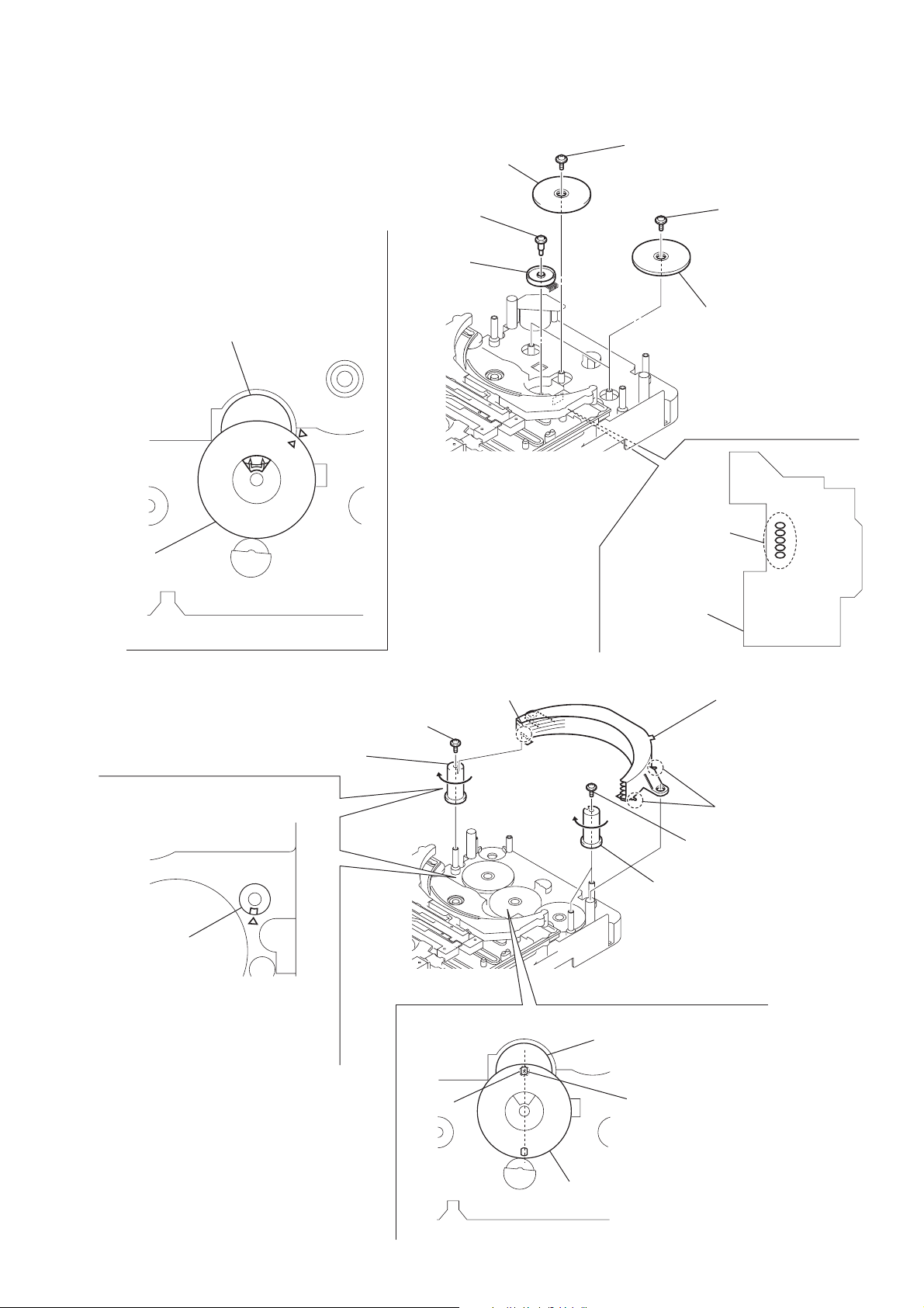
4-1. HOW TO INSTALL THE CAM (EJECT LOCK)
1
Rotate the cam (BU U/D) fully in the direction of arrow.
2
Engage the gear (eject lock) and the gear of the cam (eject lock)
aligning the mark with the center of the gear (eject lock).
cam (BU U/D)
CX-BK1
mark
gear (eject lock)
4-2. HOW TO INSTALL THE CAM (GEAR)
1
Check that the cam (BU U/D) can not be rotated in the direction of arrow.
2
Align the mark on the cam (gear) with the boss as shown in the figure
and install the cam (gear).
cam (gear)
cam (BU U/D)
cam (eject lock)
– bottom view • front –
boss
mark
– bottom view • front –
21
Page 22
CX-BK1
4-3. HOW TO INSTALL THE GEAR (MODE C)
1
Align the mark on the rotary encoder (S771) with the projection of the assy.
2
Check that the cam (BU U/D) can not be rotated in the direction of arrow.
3
Install the gear (
rotary encoder
(S771)
mode
C)
gear (
mode
C)
cam (BU U/D)
mark projection
4-4. HOW TO INST ALL THE GEAR (MODE CAM)
1
Slide the shaft in the direction of arrow.
2
Align mark A on the gear (mode cam) with mark B on the slider (mode cam) assy,
then install the gear (mode cam).
3
Check that mark C on the gear (mode cam) is in alignment with mark D on the cam (gear).
mark
A
gear (mode cam)
chassis
– bottom view • front –
shaft
slider (mode cam) assy
22
cam (gear)
mark
D
– bottom view • front –
mark
mark
B
C
Page 23
CX-BK1
2
five
solders
6
two gears
(stocker communication)
4
gear
(stocker communication)
CONNECTOR board
7
two screws
(PTPWH2.6
×
8)
5
screw
(PTPWH2.6
×
8)
3
screw
(PWH2
×
6)
rotary encoder
(S702)
gear
(stocker
communication)
– rear –
1
rotary encoder
(S702)
Engage the rotary encoder (S702)
and the gear (stocker communication)
as shown below in the figure.
4-5. HOW TO INSTALL THE ROTARY ENCODER (S702), GEAR (STOCKER COMMUNICATION)
4-6. HOW TO INSTALL THE STOCKER ASSY
To install three cams, align each groove
of the cam with each
chassis as shown in the figure.
cam
f
mark on the
3
screw
(PTPWH2.6
2
cam
(stocker V)
×
8)
screw
boss
rotary encoder
(S702)
hole
4
two cams
(stocker U/D)
Install the stocker assy
fitting three bosses into the
each groove of cam
then fix by rotating the cams
in the direction of arrow.
boss
5
two screws
(PTPWH2.6
×
8)
gear
(stocker communication)
– rear –
1
Position the hole on the gear
(stocker communication) on the
screw of the rotary encoder (S702).
23
Page 24

CX-BK1
SECTION 5
TEST MODE
[Cold Reset]
* The cold reset clears all data including preset data stored in
the RAM to initial conditions. Execute this mode when returning the set to the customer.
Procedure:
1. Press the POWER 1 button to turn off the main power.
2. While depressing the x button, press the POWER 1 button.
3. The fluorescent indicator tube does not display any message
and the set is reset.
[Version Display Mode]
*The version of the microcomputer is displayed.
Procedure:
1. Press the POWER 1 button to turn the set on.
2. T o enter the test mode, press two buttons x and POWER 1
simultaneously for more than five seconds. T he version of the
microcomputer is displayed.
[FL T ube Check]
* All fluorecent segments are tested.
Procedure:
1. Insert a disc, and extract an AC plug.
2. While depressing the [FUNCTION] button, insert an AC plug
to enter the test mode.
3. The message “CD TEST” is displayed, the initialization is
performed.
Then all segments of the fluorecent indicator tube are turned on.
[CD Ship Mode]
*This mode moves the optical pick-up to the position durable
to vibration. Use this mode when returning the set to the customer after repair.
Procedure:
1. Press the
2. Set the FUNCTION to CD.
3. Press the x button for more than five seconds.
4. After a message “MECHA LOCK” is displayed on the fluorescent indicator tube, the CD ship mode is set and the power
is turned off.
POWER 1 button to turn the set on.
sage “EQ MAX”, “EQ MIN” or “EQ FLAT” is displayed in
this order.
[AM Channel Step 9 kHz/10kHz Selection Mode]
* Either the 9 kHz step or 10 kHz step can be selected for the
AM channel step.
Procedure:
1. Set the FUNCTION to AM.
2. While depressing the
ton.
3. The channel step is changed over.
[CD Test Mode]
*This mode can run the CD sled motor freely. Use this mode,
for instance, when cleaning the pickup.
Procedure:
1. Extract an AC plug.
2. While depressing the [FUNCTION] button, insert an AC plug
to enter the CD test mode. The message “CD TEST” is displayed.
3. With the CD in stop status, press the > button to move the
pickup to outside track, or press the . button to inside track.
4. When press the B button, normal playback is performed.
5. Each time the B button is pressed during normal playback,
the tracking servo is switched on or off.
[CD Repeat 5 Times Limit Release Mode]
Procedure:
1. Press the POWER 1 button to turn the set on.
2. Select the FUNCTION to CD.
3. Press three buttons of x and [FUNCTION] and B simultaneously.
4. The repeat all mark blinks and then repeat 5 times limit is
released.
[BAND] button, press the POWER 1 but-
[Disc T ray Lock]
The disc tray lock function for the antitheft of an demonstration
disc in the store is equipped.
Setting Procedure :
1. Press the POWER 1 button to turn the set on.
2. Press two buttons of x and Z simultaneously for five seconds.
3. The message “LOCKED” is displayed and the tray is locked.
Releasing Procedure :
1. Press two buttons of x and Z simultaneously for five seconds again.
2. The message “UNLOCKED” is displayed and the tray is unlocked.
Note : When “LOCKED” is displayed, the tray lock is not released
by turning power on/off with the POWER 1 button.
[AMP Test]
*This mode is used to check the function of the amplifier.
Procedure:
1. Extract an AC plug.
2. While depressing the [GEQ] button, insert an AC plug to enter the AMP test mode. The message “AMP TEST” is displayed.
3. The message “Volume MAX” is displayed, when the [VOL-
UME] knob is rotated clockwise. The message “Volume 0” is
displayed, when the [VOLUME] knob is rotated counterclockwise.
4. Each time the [BASE] or [TREBLE] knob is turned, the mes-
24
Page 25
SECTION 6
)
MECHANICAL ADJUSTMENTS
CX-BK1
SECTION 7
ELECTRICAL ADJUSTMENTS
• TAPE MECHANISM DECK SECTION
Note: Tape deck is not loaded in US model.
Precaution
1. Clean the following parts with a denatured alcohol-moistened
swab:
record/playback heads pinch rollers
erase head rubber belts
capstan idlers
2. Demagnetize the record/playback head with a head
demagnetizer.
3. Do not use a magnetized screwdriver for the adjustments.
4. After the adjustments, apply suitable locking compound to the
parts adjusted.
5. The adjustments should be performed with the rated power
supply voltage unless otherwise noted.
Torque Measurement
Mode
FWD
FWD
back tension
REV
REV
back tension
FF/REV
FWD tension
REV tension
Torque meter
CQ-102C
CQ-102C
CQ-102RC
CQ-102RC
CQ-201B
CQ-403A
CQ-403R
Meter reading
2.94 – 7.84 mN • m
(30 to 79 g • cm)
(0.42 – 1.11 oz • inch)
0.15 – 0.6 mN • m
2 to 6 g • cm
(0.03 – 0.08 oz • inch)
2.94 – 7.84 mN • m
(30 to 79 g • cm)
(0.42 – 1.11 oz • inch)
2.94 – 7.84 mN • m
(30 to 79 g • cm)
(0.42 – 1.11 oz • inch)
6.86 – 17.64 mN • m
(70 to 179 g • cm)
(0.98 – 2.49 oz • inch)
9.8 mN • m
(100 • cm or more)
(1.4 oz • inch or more)
9.8 mN • m
(100 • cm or more)
(1.4 oz • inch or more)
DECK SECTION
Note: Tape deck is not loaded in US model.
0 dB = 0.775 V
Precaution
1. Demagnetize the record/playback head with a head
demagnetizer.
2. Do not use a magnetized screwdriver for the adjustments.
3. After the adjustments, apply suitable locking compound to the
parts adjust.
4. The adjustments should be performed with the rated power
supply voltage unless otherwise noted.
5. The adjustments should be performed in the order given in
this service manual. (As a general rule, playback circuit adjustment should be completed before performing recording
circuit adjustment.)
6. The adjustments should be performed for both L-CH and RCH.
7. Switches and controls should be set as follows unless otherwise specified.
• Test Tape
Tape Signal Used for
P-4-A100 10 kHz, – 10 dB Azimuth Adjustment
WS-48B 3 kHz, 0 dB Tape Speed Check
Record/Playback Head Azimuth Adjustment
Procedure:
1. Mode: Playback
test tape
P-4-A100
(10 kHz, – 10 dB)
SPEAKER board
SPEAKER terminal (JK502
L-CH, R-CH
set
level meter
+
–
2. Turn the adjustment screw and check output peaks. If the peaks
do not match for L-CH and R-CH, turn the adjustment screw
so that outputs match within 1dB of peak.
Output
level
within
1dB
L-CH
peak
R-CH
peak
within
1dB
Screw
position
L-CH
peak
R-CH
Screw
position
peak
25
Page 26
CX-BK1
)
3. Mode: Playback
SPEAKER board
test tape
P-4-A100
(10 kHz, – 10 dB)
L-CH
set
R-CH
in phase 45°90°135°180
SPEAKER terminal (JK502)
L-CH
R-CH
waveform of oscilloscope
good
oscilloscope
V
wrong
H
°
4. After the adjustments, apply suitable locking compound to the
parts adjusted.
Adjustment Location:Record/Playback/Erase Head
Record Bias Adjustment
Procedure:
1. Record mode
MAIN board
AUX IN jack (JK602)
1) 315 Hz
AF OSC
2) 10 kHz
attenuator
600
2. Mode: Playback
i-Bass OFF
BASS 0
TREBLE 0
recorded
portion
set
SPEAKER board SPEAKER terminal (JK502
50 mV (–23.8 dB)
Ω
set
level meter
blank tape
CN-123
+
–
adjustment screw
Tape Speed Check
Mode: Playback
test tape
WS-48B
(3 kHz, 0 dB)
3. Confirm playback the signal recorded in step 1 become
adjustment level as follows.
4. If these levels do not adjustment level, adjustment the SFR451
(L-CH) and SFR452 (R-CH) to repeat steps 1 and 4.
Adjustment level: Playback output of 315 Hz to playback out-
put
of 10 kHz: 0 ± 1.0 dB (0 ± 4.5mV).
Adjustment Location:DECK board (Page 27)
frequency counter
set
SPEAKER board
SPEAKER terminal (JK502)
L-CH, R-CH
+
–
1. Insert the WS-48B into the deck.
2. Press the B button.
3. Confirm that the frequency counter reads 3,000 ± 90 Hz.
Sample value of Wow and Flutter: 0.3% or less W.RMS (JIS)
(WS-48B)
26
Page 27
– DECK Board (Component Side) (Except US model) –
CX-BK1
SFR451
Record Bias
Adjustment
(L-CH)
– MAIN Board (Conductor Side) –
SFR452
Record Bias
Adjustment
(R-CH)
JK602
AUX IN jack (R-CH)
AUX IN jack (R-CH)
– SPEAKER Board (Conductor Side) –
SPEAKER terminal
(R-CH)
JK602
SPEAKER terminal
(L-CH)
27
Page 28
CX-BK1
CD SECTION
Note:
1. Use YEDS-18 disc (3-702-101-01) unless otherwise indicated.
2. Use an oscilloscope with more than 10M Ω impedance.
3. Clean the object lens by an applicator with neutral detergent when the
signal level is low than specified value with the following checks.
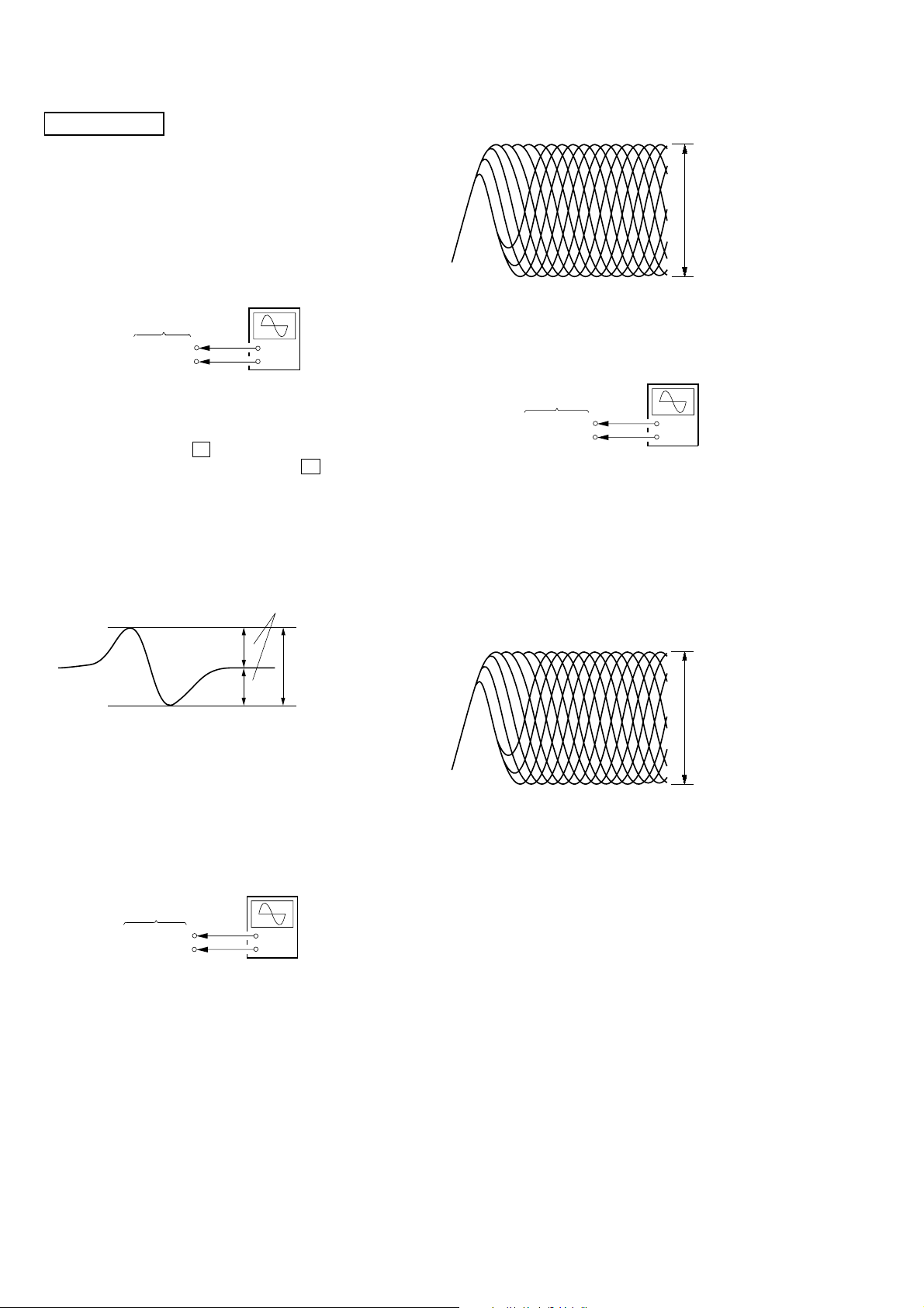
S-curve Check
Connection:
oscilloscope
BD board
TP (FE)
TP (VC)
Procedure:
1. Connect an oscilloscope to test point TP (FE) and TP (VC)
on the BD board.
2. While depressing the button, insert an AC plug.
B
3. Put the disc (YEDS-18) in and press the button and
actuate the focus search. (actuate the focus search when disc
table is moving in and out)
4. Check the oscilloscope waveform (S-curve) is symmetrical
between A and B. And confirm peak to peak lev el within 2 ± 1
Vp-p.
S-curve waveform
+
–
symmetry
A
B
x
within 2
±
1 Vp-p
RFDC signal waveform
VOLT/DIV: 200 mV
TIME/DIV: 500 ns
level: 0.6
±
0.15 Vp-p
Checking Location: CD board (Conductor side)
RFAC Level Check
Connection:
oscilloscope
BD board
TP (RFAC)
TP (VC)
+
–
Procedure:
1. Connect an oscilloscope to test point TP (RFA C) and TP (VC)
on the BD board.
2. Turn the power on.
3. Put the disc (YEDS-18) in to playback the number five track.
4. Confirm that oscilloscope waveform is clear and check RF AC
signal level is correct or not.
Note: A clear RFAC signal waveform means that the shape “◊” can be
clearly distinguished at the center of the waveform.
RFAC signal waveform
VOLT/DIV: 200 mV
TIME/DIV: 500 ns
Note: •Try to measure se veral times to make sure than the ratio of A : B
or B : A is more than 10 : 7.
•Take sweep time as long as possible and light up the
brightness to obtain best waveform.
Checking Location: BD board (Side B)
RFDC Level Check
Connection:
oscilloscope
BD board
TP (RFDC)
TP (VC)
+
–
Procedure:
1. Connect an oscilloscope to test point TP (RFDC) and TP (VC)
on the BD board.
2. Turn the power on.
3. Put the disc (YEDS-18) in to playback the number five track.
4. Confirm that oscilloscope waveform is clear and check RFDC
signal level is correct or not.
Note: A clear RFDC signal waveform means that the shape “◊” can be
clearly distinguished at the center of the waveform.
Checking Location: BD board (Side B)
level: 1.0
±
0.4 Vp-p
28
Page 29
CX-BK1
E-F Balance Adjustment
Connection:
oscilloscope
BD board
TP (TE)
TP (VC)
+
–
Procedure:
1. Connect an oscilloscpe to test point TP (TE) and TP (VC) on
the BD board.
B
2. AC is put in pushing
button to enter the CD test mode.
3. Put the disc (YEDS-18) in to playback the number five track.
B
4. Press the button. If it plays, press the button again.
B
(The tracking servo and the sledding servo are turned OFF)
5. Rotate RV101 on the BD board to adjust A (DC voltage) of
the center of the oscilloscope waveform becomes 0 V.
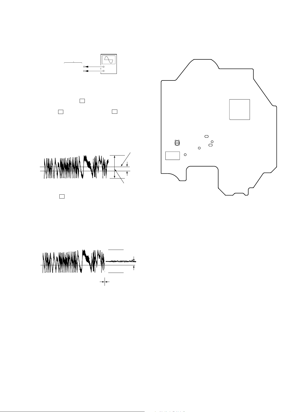
Traverse Waveform
0V
Center of
the waveform
B
A (DC
voltage)
Checking Location:
– BD BOARD (Side B) –
RV101
E-F Balance
Adjustment
TP7
(VC)
IC103
TP2
(TE)
TP8
(RFAC)
IC101
TP6
(RFDC)
TP4
(FE)
level: 1.0 ± 0.5 Vp-p
6. Press the button. (The tracking servo and sledding servo
B
are turned ON)
Confirm A (DC voltage) at that tome is 0 V.
7. To exit from this mode, turn the power off.
Notes: •Always move the optical pick-up to most inside track when
0V
exiting from this mode. Otherwise, a disc will not be unloaded.
• Do not run the sled motor excessively, otherwise the gear can
be chipped.
Traverse Waveform
Tracking servo
Sled servo
OFF
Tracking servo
Sled servo
ON
A (DC
voltage)
Checking Location: BD board (Side B)
Adjustment after CD Base Unit (BU-30CBD64NS) is Replaced
Perform the “E-F Balance (1 track jump) check”.
29
Page 30

CX-BK1
MEMO
30
Page 31

8-1. BLOCK DIAGRAM – CD Section –
OPTICAL PICK-UP
BLOCK
VC
2
VCC
4
PD1
7
PD2
5
I5-10
3
I1-6
1
LD
GND
PD
VR
F+
FOCUS
COIL
F-
COIL
T+
T-
TRACKING
VDD (3.3V)
POWER CONTROL
E-F BALANCE
(1 TRACK JUMP)
(SLED)
(SPINDLE)
AUTOMATIC
Q101
RV101
M102
M101
M
M
RF AMP
IC103
VC
27
A
6
RFDCI
B
7
C
8
D
9
E
10
F
11
LD
1
19
PD
2
MOTOR/COIL DRIVE
IC102
VO1+
52
VO1-
47
VO2+
56
VO2-
55
VO3+
2
VO3-
1
VO4+
10
VO4-
5
RF AC
RFDC
FE
FEI
TE
SWTE_BAL
IN1+
IN1-
IN2+
IN2-
IN3+
IN3-
IN4R
STBY
SECTION 8
DIAGRAMS
15
28
29
16
17
18
12
35
34
32
31
27
26
24
8
DIGITAL SERVO,
DIGITAL SIGNAL PROCESSOR
IC101
D OUT
RFAC
50
RFDC
43
FE
39
TE
41
SE
40
FFDR
33
FRDR
34
TFDR
31
TRDR
32
SFDR
29
SRDR
30
MDP
25
PCMD
BCLK
LRCK
XTAI
XTAO
DATA
CLOK
XLAT
SQCK
SCLK
SCOR
SQSO
SENS
64
66
67
65
71
72
4
6
5
77
8
15
76
7
X201
16.9344MHz
D/A CONVERTER,
MP3 DECODER
SDIO
12
BCKIA
13
LRCKIA
14
XI
62
XO
63
IC104
MIDIO
STAND BY
RESET
MICK
MICS
REQ
MILP
CX-BK1
• R-ch is omitted due to same as L-ch.
• SIGNAL PATH
: CD
: DIGITAL OUT
OPTICAL
TRANSCEIVER
IC604
LO
23
RO
26
R-CH
5
19
6
7MIACK
1
3
39
4
DIGITAL
OPTICAL
OUT
(AEP, UK)
SYSTEM CONTROLLER
IC901 (1/3)
IO-MIDIO
64
38
O-MP3STB
O-MICK
62
I-MIACK
37
O-MP3RST
19
5
O-MICS
I-MP3REQ
65
66
O-MILP
O-DATA
52
O-CLOCK
55
O-XLT
60
O-SQCK
57
I-SCOR
21
I-SQSO
56
I-SENS
58
O-ELV_POS
O-ELV_NEG
O-LOD_NEG
O-LOD_POS
O-SLD_POS
O-SLD_NEG
I-SLD_E0
I-SLD_E1
I-SLD_E2
I-SLD_E3
CD-L
STOCKER MOTOR DRIVE
IC721
FIN
75
87
85
77
76
86
88
73
89
70
7
9
ROLLER MOTOR DRIVE
7
9
MODE MOTOR DRIVE
7
9
1
2
3
4
OUT1
OUT2
RIN
IC711
FIN
OUT1
OUT2
RIN
IC701
FIN
OUT1
OUT2
RIN
S771
ROTARY ENCODER (MODE)
(Page 32)
A
4
2
4
2
4
2
G
M
M
M
M761
(STOCKER)
M781
(ROLLER)
M771
(MODE)
XRST
S702
ROTARY ENCODER
2
90
I-ELV_E0
69
I-ELV_E1
67
I-ELV_E2
I-ELV_E3
68
O-XRST
61
49
51
47
59
O-PWM3
O-PWM2
O-PWM1
O-LDON
I-SW1-A
I-SW2-A
I-SW2-B
I-SW3
I-SW4
I-SW5-A
I-SW5-B
I-D_SENSOR
S711 (DISC INSERT(8/12cm))
82
S713 (DISC IN (8/12cm))
79
S714 (DISC IN (8cm))
83
80
78
S717 (DISC POSITION)
84
S716 (STOCKER IN/OUT)
74
81
(STOCKER POSITION)
1
2
3
4
S715 (DISC OUT)
S718 (STOCKING)
LEVEL SHIFT
Q731
G
(ON : When disc insert)S711
S713
(ON : Play position)
S714
(ON : When disc out from play position)
S715
S718
S717
S716
DISC INSERT
DETECT SENSOR
IC751
ON : Play position
(8cm disc only)
OFF: In the Midst disc is moving
between play position and
stocker
In the midst disc is moving
between play position and stocker
ON : disc is play position side
OFF : disc is stocker side
ON : The moment disc in/out
from stocker
3131
Page 32

CX-BK1
8-2. BLOCK DIAGRAM – TUNER/TAPE/USB Section –
(EXCEPT US)
HRPE1
(REC/PB/ERASE)
D –
CD-L
A
SFR452
RECORD
BIAS (R)
J700
(USB)
3
D+
2
1
(Page 31)
FM 75 Ω
(COAXIAL)
AM LOOP
L-CH
R-CH R-CH
ERASE
VBAS
R-CH
AUDIO
USB ON/OFF
SWITCH
Q702
USB VBUS ON
(Chilean, Peruvian, Mexican)
J201
FM/AM TUNER PACK
TUNER-L
FM ANT
REC SWITCH
Q305 – 308
BIAS OSC
L451
IC700
FOUTR
XTI
1 2
X700
12MHz
R-CH
MDATA
MCLK
PLLCE
TUNED
STEREO
RDS DATA
RDS CLK
RDS SIG
(AEP, UK)
BIAS OSC
Q453, 454
R-CH
34FOUTL
37
XTO
DO
R-CH
R-CH
AUX IN
MUTING
Q443
REC/PB
REC MUTE
REC BIAS
SWITCH
Q451
BIAS
JK603
VIDEO OUT
JK602 (1/2)
L
R
39 FINR
SDA21SCL13ACK12INT_DATA
20
USB ACK
USB CLK
USB DATA
USB INT
R-CH
+12V
R-CH
5OUTL
6OUTR
PB AMP
IC301
REC AMP
IC401
TUNER-R
AM ANT
FM SIGNAL OUT
VIDEO
DO
DI
CLK
CE
TUNED
STEREO
RDS DATA
RDS INT
MUTING
Q309
R-CH
SFR451
RECORD
BIAS (L)
J701
LINE IN
L
R
USB INTERFACE
26 D+ 36 FINL 15 X2
25 D –
23 VBUS
MIC
R-CH
IC201 (1/2)
LINE AMP
Q605
R-CH
AUX AUDIO
SELECTOR
14 X1
12 X0
MIC LEVEL
AGC
Q201
MIC AMP
MUTING
Q607
Q608
IC501
COM X
BA
10 9
B
A
VR201
MIC MIXING
R-CH
13
MIC AMP
IC201 (2/2)
JK602 (2/2)
• R-ch is omitted due to same as L-ch.
• SIGNAL PATH
: CD
: TUNER
: TAPE PLAY
: REC
: USB
INPUT SELECT
IC601 (1/2)
MIC
2
CD-L
40
TUNER-L
39
TAPE-L
38
AUX-L
37
RECB-2
35
L
AUX OUT
R
SHIFT REGISTER
IC703
BIAS
REC MUTE
REC/PB
A
B
6Q0
7Q1
8Q2
SO
18 3
3
DATA
14 Q8
9Q3
16 Q10
SHIFT REGISTER
IC701
TOUTL
DATA
4 5
4 5
Q10
CLOCK
CLOCK
SO
LCK
LCK
10Q4
11Q5
12Q6
13Q7
14Q8
15Q9
16
17Q11
18
15Q9
10Q4
29
9Q3
7Q1
8Q2
6Q0
V-BASS
SHIFT SO
TUNER ON
18
19
20
21
22
23
24
INH
USB ON
CD ON
DO
MDATA
MCLK
PLLCE
TUNED
STEREO
(AEP, UK)
RDS-DATA
RDS-CLK
RDS-SIG
USB VBUS
USB DATA
USB CLK
USB ACK
USB INT
CLK
MDATA
LCK
MCLK
SYSTEM CONTROLLER
IC901 (2/3)
6 I-DO
50 O-MDATA
48 O-MCLK
46 O-PLLCE
9 I-TUNE
8 I-STEREO
2 I-RDS_DATA
20 I-RDS_CLK
1 I-RDS SIG
(AEP, UK, Chilean, Peruvian)
33 I-USB_VBUS_ON
24 I2C-USB_DATA
25 I2-USB_CLK
31 I-USB_ACK
32 I-USB_INT
44 O-SHIFT_DATA
43 O-SHIFT_CLK
45 O-SHIFT_STB
: MIC
: AUX IN
: LINE IN (AUDIO)
: VIDEO
BAND-PASS
99I-LEVEL
27I-DECK_ENDSW
28I-DECK_PACK
29I-DECK_FREC
30I-DECK_RREC
26I-DECK_PLAYSW
PLUNGER DRIVE
CAPSTAN/REEL
MOTOR DRIVE
Q905
Q904
FILTER
Q902
OUT-L
V-BASS,
18 – 24
MDATA, MCLK,
LEVEL
LEVEL
TAPE MECHANISM
DECK BLOCK
END SW
PACK
F_REC
R_REC
PLAY SW
(DECK-A)
A-SOL
(CAPSTAN/REEL)
CAPM+
INH, SHIFT SO,
CLK, LCK
USB ON,
CD ON, TUNER ON
B
C
D
(EXCEPT US)
MM
E
F
(Page 33)
(Page 33)
(Page 33)
(Page 33)
(Page 34)
3232
Page 33

CX-BK1
8-3. BLOCK DIAGRAM – AMP Section –
• R-ch is omitted due to same as L-ch.
• SIGNAL PATH
: TUNER
BASS BOOST ENHANCER
IC603
(Page 32)
(Page 32)
(Page 32)
OUT-L
B
V-BASS,
18 –24
C
MDATA, MCLK,
LEVEL
D
BBE ON/OFF
CONTROL
Q623
V-BASS
1
INA
BBE14VREF12GOUT
7
FREQUENCY
CONTROL
Q614 – 616
19
18
6
OUTA 25OUT 2
GIN
13
BOOST
CONTROL
Q617 – 620
23
20
222124
R-CH
+
FEED BACK
SWITCH
Q625
BOOST
CONTROL
Q624
ELECTRICAL VOLUME
IC601 (2/2)
28 VOLIN2
DATA22CLOCK
21
MCLK
MDATA
SAOUT
19
LEVEL
M301
FAN MOTOR
Q301 – 303
R-CH
RELAY DRIVE
Q530
(FAN)
MM
DRIVE
+
THERMAL DETECT
POWER
POWER MONITOR
JK502
5 SPEAKER
+
–
+
–
J521
PHONES
L
R
G
H
(Page 34)
(Page 34)
SWITCHING
Q618
R-CH
SWITCHING
Q619
R-CH
CURRENT
MIRROR
Q521, 523
PRE DRIVE
Q517
27BB_A2
26BB_B2
R-CH
D611
MUTING
Q525
MUTING
CONTROL
Q527
R-CH
+
OVER CURRENT
DETECT
Q013
X901
32.768kHz
R-CH
CASCADE
Q511, 513, 515
X902
5MHz
BIAS
Q507, 509
–VP
+VP
FINAL DRIVE
Q531, 533
R-CH
OVER LOAD
DETECT
Q505
+
HOLD
Q012
+
+VH
+VL
– VH
– VL
OUTPUT LEVEL
DETECT
Q620, 621
OUTPUT LEVEL
DETECT
Q617, 622 – 624
+
TH501, 502
THERMAL
DETECT
Q610, 611
R-CH
+
R-CH
RY501
(Page 32)
INH, SHIFT SO,
CLK, LCK
E
LIQUID CRYSTAL
DISPLAY
LCD001
67 – 70 1 – 65
LCD DRIVER
COM1 – COM4 S1 – S65
IC001
OSC
INH
39
O-MUTE
DI
80
CL
79
CE
78
77
76
OSC
C105, R101
INH
SHIFT SO
CLK
LCK
CLK
LCK
3
4
5
18
2
3
4
53
54
63
LED DRIVE
IC602
DATA
CLK
LCK
SO
LED DRIVE
IC601
DATA
CLK
LCK
O-LCD_DATA
O-LCD_CLK
O-LCD_CE
Q0 – Q9
Q10
Q1 – Q6
Q8, Q9
Q7
16
12
6 – 15
6 – 11
13, 14
LED DRIVE
Q601 – 605
LED203
i-Bass
LED204 – 221
(ILLUMINATION)
LED251 – 254
(LCD BACKLIGHT)
LED601
(DISC SLOT ILLUMINATION)
17 18
XT1
LED631 – 635
(DISC INDICATOR 1 – 5)
XT2
14 15
X1
STBY
34
LED202
STANDBY/ON
X2
SYSTEM CONTROLLER
IC901 (3/3)
S311 – 320, 331 – 339,
S341 – 344
VOLUME
BASS
TREBLE/MIDDLE
MULTI JOG
REMOTE CONTROL
98
I-POWER_MONI
ROTARY
ENCODER
ROTARY
ENCODER
ROTARY
ENCODER
ROTARY
ENCODER
RECEIVER
IC603
S301
S302
S303
S304
I-KEY1 – I-KEY3
97 – 95
93
I-RE_VOL
92
I-RE_BAS
91
I-RE_TRE
94
I-RE_JOG
23
I-RMC
I-HEADPHONE
O-POWER
42
40
41I-POWER_DOWN
16RESET
POWER_DOWN
RESET
J
(Page 34)
3333
Page 34

CX-BK1
8-4. BLOCK DIAGRAM – POWER SUPPLY Section –
POWER,
(Page 33)
POWER MONITOR
H
POWER MONITOR
VOLTAGE
DETECT
Q107 – 109
AC DETECT
Q105, 106
++
+VH – VH
DC UNBALANCE
DETECT
D139, 140
(Page 32)
USB ON,
TUNER ON, CD ON
F
USB ON
TUNER ON
SERVO
+2.5V
+2.5V
REGULATOR
IC121
VDD (3.3V)
USB 5V
POWER
REGULATOR
FR VDD (3.3V)
B+ SWITCH
Q024, 025
VCC 9V
+5V
IC701
+9V
REGULATOR
Q050, 051
B+ SWITCH
Q700, 701
VM 10V
TU 9V
REGULATOR
CONTROL
Q891, 892
+3.3V
REGULATOR
Q018, 019
+10V
REGULATOR
IC101
+9V
REGULATOR
Q890
M+12V,
VM, +12V
CD VM (7V),
+7V
D002
+12V
REGULATOR
IC003
+7V
REGULATOR
IC001
(US)
FAN B+
DC UNBALANCE
DETECT
D112, 113
+VL – VL
OVER CURRENT
Q102 – 104
(EXCEPT US)
DETECT
+VH
– VH
– VL
+
D116, 117
D120, 121
D114, 115
RECT
D004
+VL
RECT
D002
REG
(US, Chilean, Peruvian, Mexican)
RECT
RECT
RECT
RECT
D007 – 010
POWER TRANSFORMER
(MAIN)
PT001 (Mexican)
PT002 (Chilean, Peruvian)
PT003 (US, AEP, UK)
VH
VH
VL
VL
REG
REG
THERMAL DETECT
(Chilean, Peruvian)
VLOTAGE SELECTOR
220 – 230V
RY502
RY001
S001
120V
240V
G
(Page 33)
(AC IN)
(Page 33)
POWER_DOWN,
RESET
J
CD ON
POWER_DOWN
RESET
EVER 3.3V
RESET SIGNAL
GENERATOR
IC902
B+ SWITCH
Q901, 906
VDD
VOLTAGE
DETECT
IC904
D902
D906
+4V
REGULATOR
IC905
VSTBY
+12V
D612
POWER TRANSFORMER
PT005 (Chilean, Peruvian)
PT006 (EXCEPT Chilean, Peruvian)
RECT
D005, 006
(SUB)
RELAY DRIVE
Q101
EXCEPT
Chilean, Peruvian
3434
Page 35

CX-BK1
d
deck board (EXCEPT US)
SW (3) board
speaker motor board
SW (4) board
roller motor board
connector board
BD board
mode motor board
headphone board
right button (2) board
MIC board
LED board
jog board
USB AUX board
key LED RMC board
LCD VOL board
left button board
right button (1) board
SW (1) board
SW (2) board
8-5. NOTE FOR PRINTED WIRING BOARDS AND SCHEMATIC DIAGRAMS
Note on Printed Wiring Boards:
• X : parts extracted from the component side.
• Y : parts extracted from the conductor side.
a
•
f
•
• : Pattern from the side which enables seeing.
(The other layers' patterns are not indicated.)
Caution:
Pattern face side: Parts on the pattern face side seen from
(Side B) the pattern face are indicated.
Parts face side: Parts on the parts face side seen from
(Side A) the parts face are indicated.
: Through hole.
: internal component.
Note on Schematic Diagram:
• All capacitors are in µF unless otherwise noted. pF: µµF
50 WV or less are not indicated except for electrolytics
and tantalums.
• All resistors are in Ω and 1/
specified.
f
•
• 2 : nonflammable resistor.
• C : panel designation.
Note: The components identified by mark 0 or dotted line
• A : B+ Line.
• B : B– Line.
• H : adjustment for repair.
•Voltages and waveforms are dc with respect to ground
•Voltages are taken with a V OM (Input impedance 10 MΩ).
•Waveforms are taken with a oscilloscope.
• Circled numbers refer to waveforms.
• Signal path.
: internal component.
with mark 0 are critical for safety.
Replace only with part number specified.
under no-signal (detuned) conditions.
– BD Board –
no mark : CD PLAY
– DECK Board –
no mark : TAPE PLAY
(): TAPE REC
– USB AUX Board –
no mark : USB
– Other Board –
no mark : TUNER
(): CD PLAY
〈〈 〉〉 : TAPE PLAY
{ } : TAPE REC
[]: USB
Voltage variations may be noted due to normal production tolerances.
Voltage variations may be noted due to normal production tolerances.
F : TUNER
J : CD
c : DIGITAL OUT
E : TAPE PLAY
d : USB
j : REC
N : MIC
G : AUX IN
q : LINE IN (AUDIO)
r : VIDEO
Abbreviation
E51 : Chiliean and Peruvian models
MX : Mexican model
: Impossible to measure
∗
4
W or less unless otherwise
• Circuit Boards Location
speaker board
ACDC board
main board
PT board
tuner unit
AMP boar
3535
Page 36

CX-BK1
• Semiconductor
Location
Ref. No. Location
IC101 B-6
IC102 C-6
IC103 C-5
IC104 B-5
IC121 C-5
Q101 C-3
8-6. PRINTED WIRING BOARD – BD Board – • See page 35 for Circuit Boards Location. :Uses unleaded solder.
12
34567
A
B
C
D
R284
C272
IC104
IC101
A
IC121
CN507
(Page 43)
TP7(VC)
E
TP2(TE)
TP8(RFAC)
TP4(FE)
TP6(RFDC)
IC102
B
(Page 43)
IC103
A-MAX. 3
3636
Page 37

8-7. SCHEMATIC DIAGRAM – BD Board – • See page 42 for Waveforms. • See pag e 68 for IC Block Diagrams.
C203
1000p
TP9
CKO
220
R251
D/A CONVERTER,
MP3 DECODER
IC104
TC94A20F-CX4
R303
0
100p
C209
1k
R218
C269
47 4V
C256
0.1
C257
0.33
C270
220p
C249
0.1
220
R250
C272
0
C211
0.1
R206
1M
4.7k
R207
DIGITAL SIGNAL PROCESSOR
C255
0.1
C212
1500p
3.3k
1k
R204
R205
DIGITAL SERVO,
IC101
CXD3068Q
220p
C273
C215
0.47
B
C216
0.01
10k
100k
R202
R203
A
MAIN
BOARD
(4/4)
CN507
(Page 47)
B
MAIN
BOARD
(1/4)
CN902
(Page 44)
CN104
R216
FB102
0
C263
47 4V
10k
0.01
0.01
R271
10k
R279
100
R255
R257
R276
R259
11P
C253
R260
R261
0.1
1k
0.1
FB103
0
C261
C251
220
0.1
R351
0
0
FB351
C121
0
C122
0.1
100
R221
100
R222
1k
R220
100
R223
100
R224
100
R225
100
R226
100
R227
CN102
23P
4V
R311
L101
C314
1
0
C264
47
4V
C267
R291
C231
1000
6.3V
C229
R266
R265
220
4700p
0
IC121
BA25BCOFP-E2
0.1 0.1
C265
220
47
4V
C268
4700p
C316
0.1
FB204
0
C260
100
6.3V
C208
0
R314
4.7k
R284
220p
R275
C271
C274
R272
100
100
100
100
C266
0.1
FB203
0
C227
0.1
X201
C254
C258
0
FB201
R318
R319
0
R249
0
R321
R316
0
0
1M
C259
0.1
FB104
0
C230
C226
0.1
47 4V
R308
0
R230
150
R231
330
R232
330
R233
330
0
R310
16.9344MHz
R252
22p
1M
R253
22p
1k
560
C205
0.1
C202
0.1
CX-BK1
C292
0.1
0
FB291
C250
0.1
TP5
RFACI
C107
R104
TE
TP2
R102
0
C310
R313
0.1
C224
1
33k
R201
C313
0.1
C101
C103
470p
C115
100 10V
0
R199
SE
TP3
FE
TP4
R166
1k
R168
1k
R167
0
R169
0
C222
0.1
R219
1k
R309
0
15k
15k
R105
1k
R103
100k
B
R116
R115
33k
C102
C104
3300p
470p
C117
0.1
10k
10k
R163
R162
0.1
RV101
47k
E-F Balance
(1Track Jump)
R101
0
C133
2.2
C132
33k
RFDC
R120
33p
120k
R117
120k
R114
390k
R113
TP6
2.4k
TP7
VC
2.2k
R133
R132
330k
R131
68k
C131
0.068
0.022
R111
150k
0.1 B
C116
3300p
C213
TP8
RFAC
C112
0.1
C109
0.1
CXA2647N
IC103
C110
0.1 B
C111 C108
47 4V 0.1
R118
10k
C151
0.1
C152
0.1
R126
39k
R125
39k
C119
C118
1
1
C114
1000p
Q101
2SB970
C113
R122
100
100k
IC102
AN41020A
R155
0
R123
10V
3.3
C153
0.1
TP1
SP
CN101
16P
A-MAX. 3
M102
M101
FB161
BLM21P331
C150 C169
220 10V
220 10V
R151
100k
L163
C156
0
0.01
R152
2.2k
The components identified by mark 0 or dotted
line with mark 0 are critical for safety.
Replace only with part number specified.
3737
Page 38

CX-BK1
8-8. PRINTED WIRING BOARDS – CHANGER Section – • See page 35 for Circuit Boards Location. :Uses unleaded solder.
A
B
C
12
IC751
34567 9
8
SW (1) BOARD
(Page 43)
C
SW (2) BOARD
IC701
D
E
• Semiconductor
Location
Ref. No. Location
D701 C-4
D711 C-4
D721 C-4
IC711
IC721
SW (3) BOARD
SW (4) BOARD
S718 (STOCKING)
OFF: In the Midst disc is moving
between play position and
stocker
S717 (DISC POSITION)
In the midst disc is moving
between play position and stocker
ON : disc is play position side
OFF : disc is stocker side
S716 (STOCKER IN/OUT)
ON:The moment disc in/out
from stocker
IC701 C-4
IC711 D-4
IC721 C-4
IC751 C-2
Q731 B-5
3838
Page 39

8-9. SCHEMATIC DIAGRAM – CHANGER Section – • See page 68 for IC Block Diagram.
CX-BK1
M781
(ROLLER)
M761
(STOCKER)
CN751
3P
DIODE DIODE
IC751
DISC INSERT
DETECT SENSOR
IC751
RPR-220
+
-
+
-
D SENSE D SENSE
GND
CN781
2P
MTR RL 2
MTR RL 1
CN761
2P
MTR ST 2
MTR ST 1
CN702
3P
1
1
GND
3
3
OUT2
VREF
R702
100
D701
MTZJ-T-77-4.7B
CN703
2P
1
1
MTR RL 2
MTR RL 1
2
2
CN704
2P
1
1
MTR ST 2
MTR ST 1
2
2
C781
0.01
D721
MTZJ-T-77-3.6A
VREF
OUT2
VCC
RNF
OUT1
VM
R721
680
STOCKER MOTOR
GND
RIN
FIN
RNF
DRIVE
IC721
BA6956AN
OUT1
VM
R701
680
(DISC INSERT(8/12cm))
(ON:WHEN DISC INSERT)
VCC
FIN
MTZJ-T-77-5.6B0.01 100
MODE MOTOR
GND
RIN
DRIVE
IC701
BA6956AN
RNF
OUT1
R711
680
VCC
VM
FIN
GND
CN711 CN705
2P 2P
1
GND
SW1
2
RIN
VREF
OUT2
R712
100
D711C761 R722
S711
ROLLER MOTOR
DRIVE
IC711
BA6956AN
1
GND
SW1
2
R731
100
R733
R734
12k
R732
1k
10k
3 . 2
Q731
RT1N141
LEVEL
SHIFT
C711
10
50V
SW1
C754
0.1
C758
0.1
C756
0.1
C751
0.1
C752
0.1
C753
0.1
C764
0.1
C763
0.1
SW3
SW1
C755
0.1
SW2A
SW2B
SW5B
SW5A
SW4
C765
0.1
C762
0.1
D.SENSOR
SLD (MD) POS
SLD (MD) NEG
LOD (ROL) NEG
LOD (ROL) POS
ELV POS
ELV NEG
P02 SLD E1
CN701
27P
D+3.3V
M+12V
M+12V
MGND
MGND
SW3
SW1-A
SW2-A
SW2-B
SW5-B
SW5-A
SW4
SLD E0
SLD E2
SLD E3
ELV E0
ELV E1
ELV E2
ELV E3
ROTARY ENCODER
(STOCKER POSITION)
S702
C
MAIN BOARD
(1/4)
CN901
(Page 44)
S713
(DISC IN(8/12cm))
(ON:PLAY POSITION)
S714
(DISC IN(8cm))
(ON:PLAY POSITION(8cm DISC ONLY))
S715
(ON:WHEN DISC OUT FROM PLAY POSITION)
BETWEEN PLAY POSITION AND STOCKER
ON:DISC IS PLAY POSITION SIDE
OFF:IN THE MIDST DISC IS MOVING
BETWEEN PLAY POSITION AND STOCKER
(DISC OUT)
S716
(STOCKER IN/OUT)
ON:THE MOMENT DISC IN/OUT
FROM STOCKER
S717
(DISC POSITION)
IN THE MIDST DISC IS MOVING
OFF:DISC IS STOCKER SIDE
S718
(STOCKING)
CN721 CN706
3P 3P
11
GND
SW2-A
SW2-B
33
CN731 CN707
2P 2P
1
GND
SW3
2
CN741 CN708
4P 4P
11
GND
SW5-B
SW5-A
SW4
44
GND
SW2-A
SW2-B
1
GND
SW3
2
GND
SW5-B
SW5-A
SW4
SW2A
SW2B
SW5B
SW5A
SW4
S771
ROTARY ENCODER
CN710
MTR MD 1
MTR MD 2
7P
E1
E2
GND
E3
E4
C769
0.1
SW3
C768
0.1
C767
0.1
C766
0.1
C771
0.01
CN771
11
77
7P
E1
E2
GND
E3
E4
MTR MD 1
MTR MD 2
(MODE)
+
M771
(MODE)
-
3939
Page 40

CX-BK1
• Semiconductor
Ref. No. Location
Location
D401 F-3
8-10. PRINTED WIRING BOARD – DECK Board (Except US model) – • See page 35 for Circuit Boards Location. :Uses unleaded solder.
1 2 3 4 5 6 7 8 9
IC301 E-7
IC401 E-3
Q305 E-4
Q306 D-5
Q307 E-4
Q308 F-4
Q309 E-5
Q310 E-5
Q443 E-3
Q444 F-3
Q451 B-6
Q453 B-5
Q454 B-5
A
B
C
D
E
F
(CHASSIS)
DECK BOARD
C402
EP301
C325
C408
R412
R416
R414
R402
C404
R425
D401
C412
R404
R406
R410
IC401
5
8
R417
R418
C459
C457
R408
C406
JW314
C327
E
Q444
C458
JW317
C401
R403
R405
4
1
Q443
E
R420
C403
C405
R413
R422
BIAS OSC
R401
C409
C410
L451
C411
R409
R407
R411
R419
JW316
C413
R421
JR402
JW315
C315
C407
R415
G
R423
JR322
R399
C399
R424
Q308
GDS
C456
E
SFR451
R465
Q306
E
Q307
DS
G
D
S
Q454
JR320
JW312
C461
R319
E
Q309
Q305
E
Q310
JR319
R323
JW302
C308
R316
R318
8
5
C314
CN008
JW301
R314
FB301
R310
D
MAIN
BOARD
CN009
(Page 43)
1-688-685-12(12)
C452
C460
R459
JW307
R376
JR303
JR321
JW308
R305
R303
C303
R304
C304
R458
R460
JR318
JR304
R321
C317
R307
R453
Q451
R457
C307
R315
E
C360
C309
R308
R317
R375
JW306
JW305
JW304
JW303
R309
C313
R313
C326
IC301
1
4
R322
C318
R306
C310
C453
R456
R455
C455
C454
1
CN302
8
Q453
E
R466
R454
SFR452
C462
JR401
JW310
JR302
JW309
G
18
R-CH L-CH ERASE
4040
Page 41

8-11. SCHEMATIC DIAGRAM – DECK Board (Except US model) – • See page 42 for Waveforms.
CX-BK1
(Page 46)
CN008
11P
PB-L
REC-L
PB-R
REC-R
A-GND
REC/PB SW
VM_A
REC-MUTE
O-BIAS
DECK-D-GND
+12V
R321
0
R323
100
R322
0
C401
0.1
50V
R401
120k
R403
1k
C403 R405 R407 R409
82p 47k 1k 1.2k
C405
0.01
C406
0.01
C402
R402
120k
R406C404
47k82p
0.1
50V
R404
1k
FB301
0
R457
R453
R410R408
1.2k1k
15
C460
3.3k
C411
C412
0.1
50V
50V
C317
0.1
50V
C318
0.1
50V
10
10
R306
R399
1M
R309
C307
100
10V
R310
56
C308
100
10V
56
SS
3.9k
R307C309
47047p
R308C310
47047p
C413
0.1
C456
0.01
C452
25V
22
3
8
12
R376
1k
C326
0.022
1
IC401(1/2)
NJM14558M
TE2 2.2k
R412
15k
7
IC401(2/2)
NJM14558M
TE2
C315
R411
R375
1.2k
3
8
2
REC AMP
6
5
4
Q451
2SA1981
Y
REC BIAS
SWITCH
220
16V
15k
C360
R413
R415
C407
0.01
C408 R425
0.01 10k
R416
R414
2.2k
R458
100k
R460
33
R459
15
R317
1.2k
R313 C313
18k 0.0068
R314 C314
18k 0.0068
R318
1.2k
220
16V
680
680
D401
1SS355
C453
0.0027
C455
0.0027
C454
0.0027
C327
0.1
R315
390k
R316
390k
Q444
2SA1362G
MUTING
R455
18k
2SA1362G
MUTING
R418
10k
R456
18k
Q443
IC301(1/2)
NJM14558M
TE2
PB AMP
IC301(2/2)
NJM14558M
TE2
C409
0.0047
Q453
KTC3198GR
Q453,454
BIAS OSC
Q454
KTC3198GR
R419
6
7
5
4
1k
C410R422R417
0.004722k10k
R423
R421
22k
Q307
2SJ460
Q308
2SJ460
18k
Q305
2SJ460
C399
470p
Q305-308
Q306
KRC104
S
REC SWITCH
R454
8.2
S
R424R420
18k1k
JR303
JR304
R319
4.7k
L451
BIAS OSC
R305
220k
0
0
Q309
2SA1362G
MUTING
Q310
2SA1362G
MUTING
JR401
0
C458
0.001
C459
560p
C325
R303
82k
C303
0.0012
R304
82k
C304
0.0012
HRPE301
(REC/PB/ERASE)
CN302
8P
C462C461
C457
0.0056
100K
SFR451
33K
SFR452
33K
390p390p
R466
100K
EP301
(CHASSIS)
R465
0.1
ERASE
L-CH
R-CH
4141
Page 42

CX-BK1
p
• Waveforms
– BD Board –
– DECK Board –
– MAIN Board –
– USB AUX Board –
1 IC103 qg (RFAC) (CD play mode)
2 IC101 us (XTAO)
59.1 ns
1.2 Vp-p
3.9 Vp-p
qa Q453, 454 Base (REC mode)
11.2 µs
qs Q453, 454 Collector (REC mode)
11.4 µs
qd Q453, 454 Emitter (REC mode)
3.6 Vp-p
10.9 Vp-
wa IC901 qg (X2)
200 ns
ws IC901 qk (XT2)
30.4 µs
2.4 Vp-p
2.5 Vp-p
ea IC700 2 (XTO) (USB mode)
37 Vp-p
84 ns
– LCD VOL Board –
ra IC001 uh (OSC)
5.7
0.9 Vp-p
21.5
µ
µ
S
s
1.5 Vp-p
4242
Page 43

8-12. PRINTED WIRING BOARD – MAIN Board – • See page 35 for Circuit Boards Location. :Uses unleaded solder.
CX-BK1
1 2 3 4 5 6 7 8 9 10 11
• Semiconductor
Location
(Page 48) (Page 40)
JW984
JW966
JW968
CN102
JW995
JW996
R531
JW985
JW969
IC904
JR902
R968
JW917
R950
R928
R930
B
C905
JW941
JW918
JW970
JW919
JW986
JR901
R940
JW944
C906
CN902
USB AUX
BOARD
G
CN701
CN004
JW645
JW652
JW990
R530
R986
R529
IC905
C914
R984
D910
C933
R981
D905
D906
C932
R980
1
3
JW956
354
1
IC902
D911
R997
C910
C926
R954
JW942
C951
C950
JW924
JW923
JW920
R942
R932
R931
JW901
FM 75Ω
(AEP, UK)
JW803
CN509
(EXCEPT AEP, UK)
JW805
R784
R786
R787
JW714
R768
R982
R624
JW075
JW052
R779
R755
R778
JW038
JW651
C692
C883
(EXCEPT AEP, UK)
JW047
JW046
JR702
R788
R789
10
1
JW713
C792
JW054
R769
R983
R623
JW053
R767
R765
C791
C790
R756
R759
C691
JW055
1
10
(COAXIAL)
AM LOOP
JW048
JW974
JW972
JW971
JW722
JW715
JW915
JW056
R772
R770
R774
JW712
IC701
JW909
JW032
JW049
JW911
JW908
JW907
R773
JW037
JW910
R771
JW906
JW905
C702
20
11
(EXCEPT US)
CN009
JW045
JW044
JW709
R781
JW710
JW711
JR701
R780
JW902
JW050
JW903
JW051
C637
R628
R761
JW904
C945
JW036
JW965
JW967
JW950
JW949
JW948
JW947
JW946
JW945
JW916
R926
R924
JR908
(AEP, UK)
BD BOARD
(Page 36)
F
FM/AM/TUNER PACK
SUPPLIED WITH THE
ASSEMBLED BLOCK
A
(Page 50)
MIC BOARD
CN205
(Page 54)
R516
R524
1816
C508
R526
C630
C683
C685
R668
E
Q623
C641
R666
R655
R656
G
Q614
S
R657
D
G
Q615
JW532
JW531
JW559
JW552
JW551
JW545
JW547
JW550
JW546
JW020
(Page 36)
JR501
IC501
R669
R667
JW632
R689
S
D
R660
S
D
JW064
JW560
BD BOARD
CN506
C697
JW061
CN104
10
JR620
JW633
JW066
JW553
A
C518
C686
1
C677
Q625
G
R659
9
Q624
JW525
JW526
R521
R679
6
1
JW018
JW009
CN006
C517
R510
JW502
B5
R635
E
IC603
R680
R681
S
D
C519
R515
R523
C515
R513
R525
R511
R509
JR502
C507
CN504
C682
20
R682
11
C640
JR621
R672
R687
R688
R686
C675
G
D
Q619
S
R678
G
D
Q620
C676
R677
JW067
R636
JW505
JW011
JW022
C012
JW019
JW021
C011
C007
R003
I
AMP BOARD
CN006
(Page 54)
D501
JW522
C503
∗
CN508 15PIN CONNECTOR (AEP, UK)
CN509 11PIN CONNECTOR (EXCEPT AEP, UK)
JW643
JW501
C882
C684
R683
E
Q617
E
Q618
JR706
JR707
R685
S
JW523
JW029
C013
JR708
JR709
JR703
JR705
JR704
3
1
R684
JW801
JW554
JW025
R884
(AEP, UK)
JW024
Q051
JW017
JW043
JW008
JR801
C872
C866
D861
Q890
E
JW555
R863
(AEP, UK)
JW012
JW040
JW016
JW026
E
R053
IC101
R052
C050
C477
R880
C876
C867
Q892
JW802
C894
JW708
JW057
JW027
C052
Q050
R051
(Page 62)
R890
JW702
JW703
JW704
JW705
JW706
JW707
D050
R050
JW031
R895
JW701
JW041
JW028
E
BOARD
CN004
ACDC
C504
R885
C873
R887
CN508
JR802
R962
R893
JW804
E
R894
R892
R896
R891
Q891
E
R879
R888
C892
R881
R782
R785
R783
11
20
IC703
C700
CN007
4
JW042
1
D612
JW039
JW030
JW023
JW717
JW035
JW034
JW033
J
AMP BOARD
E
JW074
C622
C634
JW073
JW618
E
JW072
JW648
Q607
JW650
R644
R662
C618
R618
R648
E
R663
R607
JW542
CN502
(US, AEP, UK)
C624
JR601
R626
C662
JW637
JW638
C610
JR608
R606
R646
R647
R641
R645
R664
E
Q608
JW543
JW071
C019
CN502
R610
JW605
JW607
C608
R612
C602
C607
(E51, MX)
R627
R692
C666
JR624
C604
JW604
C653
C603
1
C628
21
C655
C656
C632
R622
R620
C636
JW641
JW627
R605
R670
R671
R697
Q605
E
C643
R643
C20
Q25
R031
R032
Q024
E
C018
42
IC601
22
JW611
JR610
JW612
JR611
JW616
JW613
JW614
JW644
JR614
Q602
JW626
E
R642
C638
R696
R640
R694
R695
JR617
C639
JW538
JW541
JW540
JW069
JW070
E
JW015
JW004
D017
D016
E
Q018
R018
R038
R019
C623
R616
JW606
R613
R615
(EXCEPT US)
C619
JW610
C654
C635
R619
C657
JW511
R016
D015
C601
JW536
JW537
JW608
C661
JW534
C017
JW615
R630
C631
JW512
C613
R614
JW609
C665
JR613
R629
JW549
JW535
JW065
E
Q019
R609
(EXCEPT US)
R693
C625
C627
JR612
JR615
R621
D613
JW513
C015
JW003
R017
R625
C617
C633
C621
JW514
JW006
JW007
JW556
JW557
JW558
C016
B
MAIN BOARD
C
JW602
D611
R674
C626
D
C693
R665
JW617
JW620
R604
R603
C694
C606
JR602
IC604
JW619
C672
R602
JW647
R601
Q604
R650
R652
C615
R651
R649
C614
JW649
JR607
1
C669
2
3
C668
E
R
AUX IN
L
JK602
R
AUX OUT
F
G
JK603
VIDEO OUT
DIGITAL
OPTICAL
OUT
(AEP, UK)
L
H
I
J
K
R617
JW527
C502
JW562
JW630
JW631
JW603
JW625
JW601
JW561
R698
JW058
JW059
JW533
JW628
JW629
R699
JW528
CN507
R675
C014
JW548
C611
JW544
JW639
JW529
C663
C501
C664
JW563
JW063
R517
R512
R522
JR503
R514
JW640
R676
JW621
JW622
C687
C645
C629
JW646
C696
G
Q616
R658
JW530
D018
R011
JW060
R021
R020
JW062
(EXCEPT US)
R988
R985
C936
D904
R969
C911
JW943
C946
R739
C908
JW925
R746
R934
R933
R935
R929
X901
JW940
R927
JW997
Q906
E
C901
C957
C955
R936
JW982
R987
C924
JW921
3
Q904
R992
C953
JW957
C956
R747
R938
R937
D
Q905
R989
R991
C938
Q901
C925
JR903
R999
R749
R744
JW922
R732
R939
R941
R925
R923
DECK BOARD
CN008
JW993
JW992
D907
E
R990
E
R763
JW980
C934
541
C935
C931
D902
E
X902
R947
R998
30
31
C920
R750
R753
R748
R745
R704
JW927
JW926
R754
R903
R905
R901
R963
R902
C939
C940
(Page 38)
JW994
CN903
JW981
JW953
JW976
C927
L901
JW958
C923
R703
JW930
R737
JW929
JW928
R738
R752
JW931
C
CONNECTOR
BOARD
CN701
JW955
R951
C943
C948
R733
R527
R528
JW983
R959
JW954
C944
R953
R952
(EXCEPT US)
C922
50
R734
R741
JW935
JW932
R904
CN999
JW959
R995
1 100
IC901
51
JW936
R909
R906
R730
R731
R908
JW963
JW975
R520
R639
R907
JW951
JW964
JW988
R958
(FOR CHECK)
R996
C959
C961
R913
R911
CN901
R914
R912
R910
(AEP, UK)
JW952
Q902
R960
JR904
R944
R740
R707
R723
R921
1-688-416-
JW961
R957
E
R961
R967
JR906
R943
(EXCEPT US)
JW960
R945
R701
R751
R709
R708
R713
C963
JW973
R915
R917
JW933
JR905
R916
CN905
(Page 60)
H
LCD VOL
BOARD
CN001
TAPE MECHANISM
DECK BLOCK
SUPPLIED WITH THE
R956
C930
R970
R946
R702
C909
C954
C921
C949
R710
R711
R712
R716
R920
R919
R922
JW937
JR907
R918
R955
C928
JW912
JW913
JW914
JW977
JW978
JW979
C952
C913
C915
JW962
C916
C917
C918
JW987
R760
C919
C912
R762
R764
R766
R729
81
R728
80
R727
R726
R725
R724
R714
R722
R715
JW939
R717
R718
R721
R719
JW938
JW991
JW934
JW989
C958
C962
C960
12
(12)
ASSEMBLED BLOCK
Ref. No. Location
D015 K-3
D016 K-3
D017 J-3
D018 G-4
D050 G-6
D501 B-5
D611 D-2
D612 F-6
D613 E-3
D861 C-6
D902 D-9
D904 E-8
D905 D-8
D906 D-8
D907 C-9
D910 D-8
D911 E-8
IC101 G-5
IC501 B-5
IC601 D-3
IC603 D-5
IC604 G-2
IC701 G-7
IC703 E-7
IC901 F-9
IC902 E-8
IC904 E-8
IC905 D-9
Q25 I-2
Q018 K-3
Q019 K-3
Q024 J-2
Q050 G-6
Q051 G-6
Q602 E-3
Q604 F-2
Q605 F-2
Q607 F-2
Q608 F-2
Q614 E-5
Q615 F-5
Q616 E-4
Q617 D-5
Q618 E-5
Q619 E-5
Q620 E-5
Q623 E-5
Q624 E-5
Q625 E-5
Q890 D-6
Q891 D-6
Q892 C-6
Q901 D-9
Q902 C-10
Q904 C-9
Q905 C-9
Q906 E-8
4343
Page 44

CX-BK1
8-13. SCHEMATIC DIAGRAM – MAIN Board (1/4) – • See page 42 for Waveforms. • See page 68 for IC Block Diagram.
(Page 39)
(Page 47)
(Page 45)
(Page 37)
(Page 46)
(Page 61)
ELV_E3
ELV_E2
ELV_E1
ELV_E0
SLD_E3
SLD_E2
SLD_E1
SLD_E0
SW5-B
ELV_NEG
ELV_POS
SLD_NEG
SLD_POS
LOD_NEG
LOD_POS
SW5-A
SW4
SW2-B
SW2-A
SW1-A
SW3
D.SENSOR
MGND
MGND
M+12V
M+12V
D+5V
CD_D-OUT
I2C_DATA
USB_ACK
USB_VBUS_ON
M-GND
D-OUT
D-GND
MILP
MICS
MP3REQ
MP3RST
MIDIO
MIACK
MICK
MP3STB
DGND
PWM3
PWM2
PWM1
XRST
DATA
XLT
CLOK
LDON
SQSO
SENS
SQCK
SCOR
I2C_CLK
USB_INT
TREBLE
BASS
VOL
JOG
KEY3
KEY2
KEY1
INH
CE
CL
DI
I-RMC
LCK
CLK
DATA
STBY
VDD
GND
VM
D-GND
CN901
CN902
CN905
(1/4)
27P
R910
R911
R912
R913
R914
R915
JR908
0
R923
R924
R925
R926
R927
R928
R929
R930
R931
R932
R933
R934
R935
R936
R937
R938
R939
23P
19P
R527
R528
R529
R530
R531
100
100
100
100
100
100
100
100
100
100
100
100
100
100
100
100
100
100
100
100
100
100
100
100
100
100
100
(AEP,UK)
100
M23
M22
M21
M20
M19
M18
M17
M16
M15
M14
M13
M12
M11
M10
M9
M8
M7
M6
M5
M3
M2
M1
C945
0.1
C2
C3
C4
C5
C6
C7
C8
C9
C10
C11
C12
C13
C14
C15
C16
C17
C18
C19
C20
C1
U1
U2
U3
U4
U5
K7
K6
K5
K4
K3
K2
K1
47k
R901
47k
R902
47k
R903
47k
R904
47k
R905
47k
R906
47k
R907
47k
R908
47k
R909
0.001
C958
0.001
C959
0.001
C960
0.001
C961
0.001
C962
0.001
C963
47k
R916
2.2k
R917
47k
R918
47k
R919
47k
R921
47k
R922
C939
0.1
C940
1000
16V
B6
B5
B4
B3
B2
B1
B7
M1
M3
M6
M8
M10
M12
M14
M16
M18
M20
C931
10
50V
C912
C919
C918
C917
C916
C915
C913
P1
2.7k
R940
C10
Q901
DTA114EKA-
T146
RESET SIGNAL
GENERATOR
BD4923G
10k
R719
10k
R721
10k
R722
10k
R714
1k
R724
1k
R725
1k
R726
10k
R727
10k
R728
10k
R729
1200p
1200p
1200p
1200p
0.0022
0.0022
1200p
P2
P3
68k
150k
R942
R941
11
C12
C
DTC144EKA-
IC902
Q901,906
B+ SWITCH
Q906
T146
C901
100
10V
R766
K7
R764
K6
R762
K5
R760
K4
K3
K2
K1
F8
R701
220k
F10
R702 C954
47k 0.0039
R945
∗
R946
0
)
S
R944
U
T
10k
P
E
R943
C
0
X
(E
∗
R945
(E51,MX)
4.7k
(US)
10k
(AEP,UK)
150k
D911 R968
1SS355TE-17 1k
R969
27k
T
D
D
E
D
N
S
V
G
E
R
C
C
N
N
2.7k
2.7k
2.7k
2.7k
C909
1800p
10k
1M
(AEP, UK)
C922
0.1
3
C
I-D_
SENSOR
I-SW1-A
I-SW2-B
I-SW5-A
O-LOD_NEG
O-SLD_NEG
O-ELV_NEG
I-SLD_E0
I-SLD_E2
I-ELV_E0
I-RE_TRE
I-RE_BAS
I-RE_VOL
I-RE_JOG
I-KEY3
I-KEY2
I-KEY1
I-POWER_MONI
I-LEVEL
I-SUFIX
R995
(US, E51, MX)
(AEP, UK)
R952
100k
R953
100k
C952
100p
C923
∗
0 (AEP, UK)
0 (AEP, UK)
10k (US, E51, MX)
C925
0.1
R520
470k
1
R996
C932
0.1
R920
10k
7
9
M
M
1k
10k
R712
R716
4
S
-A
O
W
2
P
W
_
I-S
D
I-S
O
-L
O
S
S
V
A
VOLTAGE DETECT
IC904
M62703ML
G
13
11
15
M
M
M
1k
1k
10k
R723
R713
R715
S
S
O
O
P
P
_
_
V
D
L
L
E
-
-S
O
O
IG
S
_
S
D
R
A
I_
T
A
)
E
D
C
_
_
S
O
D
H
R
C
AVREF0
I_
(E
S
IC
O
-M
I-D
O
T7
C943
0.001
C924
0.22F
50V
D906D902
1SS3551SS355
IO
5
2
M
M
10k
10k
R718
R717
3
W
I-S
T1
T3
R996
∗
R980
4.7k
D904 R981
1SS355 470
B6
C949 R950
23
22
M
M
10k
10k
R708
R707
1
3
2
E
E
E
_
_
_
V
V
V
L
L
E
I-E
I-E
I-L
SYSTEM CONTROLLER
µPD703260YGF-S04
C
S
G
E
1
S
X
V
R
X902
5MHz
10
100p 0
C2
C4
100
1k
R751
R741
P
IL
-M
O
IC901
-JBT-A
2
X
R947
1k
Q
E
R
3
P
-M
O
T
E
S
E
R
X901
C6
1k
R740
IO
ID
-M
IO
1
T
X
4.7M
R998
32.768KHz
18p
C910
8
C
C13
1k
1k
2.2k
R639
R731
R730
T
E
K
S
C
IC
_
R
D
X
-M
-
C
O
O
-L
O
K
T
L
S
C
R
_
3
S
P
D
2
-M
T
I-R
X
O
330k
2
T
R999
R997
∗
22p
C5
C911
C936
100
16V
17
M
10k
R711
-B
5
W
I-S
1
F
E
R
V
A
T4
22
25V
21
19
M
M
10k
10k
R710
R709
1
3
S
D
E
E
S
D
_
_
V
V
D
D
B
B
L
L
I-S
I-S
O
E
0
E
R
D
N
E
D
T
U
M
D
L
V
F
I-T
I-S
L901
T5
0
C927
R951
C944
10k
0.001
50V
D905
1SS355
C934C933
100
16V
1
2
4
2
C948
100p
17
C15
C19
C
1k
1k
2.2k
R734
R733
R752
)
)
1
2
A
A
T
T
A
A
D
D
_
_
H
H
C
C
4
(4
(
T
N
L
O
-X
D
O
-L
O
W
S
K
D
C
A
N
E
P
_
_
K
K
C
C
E
E
I-D
I-D
E
S
U
R
'T
O
C
N
A
C
I-S
C1
B3 S1
+4V REGULATOR
IC905
MM1614A
5
B
B
1k
1k
R704
R703
K
A
K
T
L
C
A
C
O
_
D
L
_
D
D
C
I-C
C
-L
-L
O
O
I-POWER_DOWN
O-MP3STB(I2C_CLK)
I-MIACK(I2C_DATA)
W
I-USB_VBUS_ON
S
Y
A
L
P
_
K
C
E
I-D
6
A5
A
S2
C905
C906
0.001
VIN VOUT
T
D
N
N
O
C
G
C914D910C935
0.1MA8100-M0.022
P
14
C
2.2k
R737
A
O-PWM2
T
A
-D
O
O-MDATA
O-PWM3
O-MCLK
O-PWM1
O-PLLCE
O-SHIFT_STB
O-SHIFT_DATA
O-SHIFT_CLK
I-HEADPHONE
O-POWER
O-MUTE
EVDD
EVSS
STBY
I-USB_INT
I-USB_ACK
10k (US, E51, MX)
A9
A8
100p
100p
C951
C950
0.001
E
IS
O
N
C953
0.022
∗
R997
(AEP, UK)
0(AEP, UK)
S1
S3
F8
R961
4.7k
R970R955
01k
1k
R746
1k
R745
1k
R744
1k
R747
1k
R748
1k
R749
1k
R753
1k
R750
1k
R739
U5
U4
U3
R761
10k
R984
100
R985
1k
A1
R986
1k
R987
1k
R988
1k
100p
C955
100p
C956
100p
C957
P1
P3
C920
1
C921
1
2SB1068TP
CAPSTAN/REEL
MOTOR DRIVER
2SB1116-TP
PLUNGER
DRIVE
D907
1SS355
F4
F5
T6
S1
S3
S2
F9
F6
F7
D3
D4
B7
C9
C7
100p
0.001
C946
C908
Q904
Q905
-LK
C930
0.001
C928
22
50V
B2
B1
R982
100k
R983
100k
2SC3052F-T
BAND-PASS
R957
0
R989
R990
R991
R992
R763
Q902
1-LF
FILTER
D
D
C16
C18
C20
1k
1k
2.2k
R738
R754
R732
)
)
)
T
K
Q
E
L
E
S
C
R
E
_
_
R
E
H
_
T
C
S
U
Y
(4
S
(M
(S
N
O
K
E
S
C
Q
Q
I-S
S
I-S
I-
C
C
E
E
R
R
R
_
F
K
K
C
C
E
E
I-D
I-D
A
T
A
K
L
D
_
C
_
B
B
S
C
S
-U
M
-U
C
I2
I2
I-R
2
1
U
U
R954
A7
10k
C926
0.001
R960
220k
R959
1.5k
R958
39k
S3
S2
47k
A5
A6
47k
A8
47k
A9A2
47k
A7
47k
C938
R967
CN999
CN903
F4
F5
F6
F7
1
50V
100
F9
F10
T1
T2
T3
T4
T5
T6
T7
S1
S2
S3
A1
A2
7P
8P
EVER3.3V
INH
O-SHIFT_SO
RESET
FLMDCO
SO
SCK
SI
VDD
GND
END SW
GND
SOL
MOTOR
PACK
F.REC
R.REC
PLAY SW
MDATA
MCLOCK
POWER
MUTE
LEVEL
A-GND
HEADPHONE
O-POWER-MONITOR
RDS-DATA
RDS-CLK
TU-SIG(ECHO_CE)
STEREO
TUNED
CE
DO
O-SHIFT_STB
O-SHIFT_CLK
O-SHIFT_DATA
V-STBY
FR-VDD(3.3V)
FR-GND
+12V
MOTOR
SOL
VM_D
(FOR CHECK)
TAPE MECHANISM
DECK BLOCK
SUPPLIED WITH
THE ASSEMBLED
BLOCK
(Page 46)
(EXCEPT US)
(Page 46)
4444
Page 45

8-14. SCHEMATIC DIAGRAM – MAIN Board (2/4) –
(2/4)
(Page
49)
(AEP,UK)
(Page 44)
(E51,MX)
(Page 51)
DIGITAL
OPTICAL
OUT
CD_D-OUT
D-GND
I2C_CLK
I2C_DATA
USB_ACK
USB_INT
USB_VBUS_ON
USB_ON
VM
D-GND
V-IN
V-GND
D-GND
A-GND
USB-L
USB-R
A-GND
AUX2-L
AUX2-R
AUX OUT
VIDEO OUT
AUX IN
CN504
JK603
L
R
L
R
IC604
GP1FA313TZ
OPTICAL
TRANSCEIVER
5P
MIC-A-GND
MIC-OUT
I-MIC
VM
LCK
CN004
17P
1P
JK602
4P
I-MIC
LCK
I2C_CLK
I2C_DATA
USB_ACK
USB_INT
USB_VBUS_ON
USB_ON
R607
0
0
JR607
C504
4.7
50V
C606
0.1
R601
R603
4.7k
R602
4.7k
22k
R604
22k
R651
47k
R652
47k
R521 R522
00
C501 C502
10
50V
C615
C694
0
R525
100
C503
4.7
50V
100
R526
0.001
C614
0.001
R513
22k
R514
22k
R524
0
R512
22k
10
50V
R650
0
2SD1306NE
MUTING
22k
R511
Q604
C668 C669
47
16V
C508
CX-BK1
0.1
C664
10
50V
R515
COM X
22k
R518
100
VDD
X2
X1
X0
X3
A
B
C507
Q607
2SD1306NE
MUTING
Q602
2SC3052F-T
1-LF
LINE AMP
R605
27k
R517
100
R509
10k
0.1
A
R510
10k
B
R523
0
(E51,MX)
R627
4.7k
R640
2.2M
R694
2.7k
R696
100k
C638
100
25V
R516
22k
D501
UDZSTE173.9B
C519
100 10V
C518
100 10V
C517
0.1
AUX AUDIO SELECTOR
IC501
BU4052
Y0
Y2
0.1
R649
0
R644
2.2k
R648
4.7k
COM Y
Y3
Y1
INH
VEE
VSS
R647
4.7k
JR616
C610
4.7
50V
0
R642
1.2k
R676
2.2k
R699
5.6k
L
-
-L
E
R
E
P
A
N
T
U
T
R643
1.2k
R645 C643
2.2k 4.7
50V
C613
4.7
50V
R692
100
R670
100
TUNER-R
TAPE-R
REC-R
R609
0
R698
5.6k
C665
220p
INPUT SELECT/
ELECTRICAL
VOLUME
IC601
M61529 FP
(US,AEP,UK)
JR624 C666
0 220p
0
R616
R614
0
(EXCEPT US)
R610
0
C692
4.7 50V
C603
C653
100
470p
16V
C663
10
50V
0
R675
2.2k
R615
C611
4.7
50V
R693
100
R630
10k
C619
0.047
2
-L
PL
PL1
CD
1/D
R2/D
U
UR
S
S
-R
IC
EF
CD
R
M
C604
4.7
50V
C601
10
50V
)
S
0
R613
(EXCEPT U
-L
X-L
ER
AU
TAPE-L
TUN
-R
-R
-R
NER
TAPE
TU
AUX
C602
10
50V
R617
2.2k
50V
0.022
1
C623
C621
I2
TM
ECB-2
R
-1
I1
RECB
TM
C624
0.022
1
50V
C622
R618
2.2k
C639
100
25V
Q605
2SC3052F-T
1-LF
LINE AMP
C617
10
50V
R625
10k
0.022
0.0027
0.047
C633
C627
C625
O2
M
T
O1
TM
0.022
C634
CC2
TCA2
TCB2
T
C1
A1
B1
TC
TC
TC
C626
0.047
C628
0.0027
R626
10k
C618
10
50V
R695 R697
2.7k 100k
JR617
0
4
3
X
X
0
0
JR613
JR612
UT2
O
T
T1
IN1
U
TO
VOL
0
0
JR611
JR610
2
1
X
X
R671
100
-L
C
E
R
R606
27k
R641
2.2M
IN2
VOL
C691
4.7
50V
JR615
0
R621
15k
1k
0.22
0.22
C661
220p
R619
C635
C631
2
T2
_A
_B2
U
B
O
B
BB
1
T1
B-B1
SAOUT
B
OU
BB-A
1k
0.22
0.22
R620
C636
C632
R622
15k
L
E
V
E
L
JR614
0
C655
270p
T
D
CK
N
OU
G
W
CLO
S
TA
DA
VCC
C637
10
25V
R623 R624
2.2k 2.2k
R628
22k
A
T
A
D
-M
O
10
1SS355
R629
D613
C656
0.1
C657
100
16V
220p
C662
270p
C654
K
C
O
L
C
-M
O
R662
0
C693
0.47
50V
REC-OUT-MUTE
2SA1235TP
INVERTER
R664
18k
Q608
R663
10k
D611
1SS355
R674
100k
1M
R665
A1
A2
A3
A4
A5
A6
A7
A8
A9
A10
A11
(Page 46)
B6
B1
B2
B3
B4
B5
B7
B8
B9
B10
(Page 47)
4545
Page 46

CX-BK1
8-15. SCHEMATIC DIAGRAM – MAIN Board (3/4) – • See page 68 for IC Block Diagrams.
(Page 44)
R
L
O
S
E
N
O
H
P
D
A
E
5
Z
I-H
1-LF
R892 R891
2.2k 2.2k
O
IT
N
A
O
T
B
K
E
A
T
L
N
-M
S
C
D
O
R
_
_
_
E
H
T
T
T
P
W
IF
IF
IF
D
O
H
H
H
A
P
S
E
-
-S
-S
-
H
O
O
O
O
R
O
IT
N
O
M
_
5.6k
5.6k
5.6k
R
E
W
R767
R765
R769
O
-P
O
1
2
3
Z
Z
Z
Q890
KTA1266GR
+9V
REGULATOR
2SC3052F-T
1-LF
R881
47k
C894 R890
0.1 47k
R888 R879
100 1k
C892
47
16V
O
S
V
_
T
.3
3
IF
R
H
E
S
H
-
V
IN
O
E
8
9
Z
Z
(AEP,UK)
C867
0.01
)
E
C
_
O
H
C
A
T
K
(E
A
L
-D
-C
S
S
D
D
R
R
O
D
E
IG
E
R
N
-S
E
O
T
E
U
U
S
T
C
T
D
Y
D
L
B
E
D
E
N
T
T
_
V
E
L
U
-G
M
-S
M
V
A
V
)
V
.3
(3
D
N
-G
R
F
K
D
D
V
-V
2
1
R
F
+
R
C
A
T
O
A
L
D
C
M
M
R
E
O
T
W
O
O
P
M
(3/4)
K
R
C
A
T
Y
1
Y
I-MIC
LCK
C876
C872 C873
4.7
0.0033 0.0033
50V
R884
R880
3.9k
5.6k
C882
4.7
A1
A2
A3
A4
A5
A6
50V
TUNER-L TUNER-R
2
3
Y
Y
R885
R887
3.9k
5.6k
C883
4.7
50V
L
4
5
E
Y
Y
V
E
L
C477
4.7
50V
E
B
T
T
U
S
M
V
A
D
-M
O
E
O
L
W
C
O
M
-
-P
4
O
Z
O
Q891,892
R893
REGULATOR
10k
CONTROL
R894
0
R895
Q892 Q891
2.2k
2SC3052F-T
R896
2.7k
(Page 44)(Page 44)
N
O
_
S
A
U
K
T
T
B
V
_
B
S
U
N
O
_
S
U
B
V
_
B
S
U
C866
10
50V
R863
68
K
C
A
L
IN
A
D
C
_
_
_
_
B
B
C
C
S
S
U
U
I2
I2
A
K
T
T
K
C
A
L
A
IN
C
D
_
_
_
_
B
B
C
C
S
S
I2
I2
U
U
Y1
R962
10k
Y2
Y3
Y4
Y5
JW011
(AEP,UK)
RDS DATA
RDS INT
FM SIGNAL OUT
+3V(RDS)
TU-MUTE
TUNER-R
GND
TUNER-L
STEREO
TUNED
VM+9V
CE
DI
DO
CLK
TU-MUTE
TUNER-R
GND
TUNER-L
STEREO
TUNED
VM+9V
CE
DI
DO
CLK
(EXCEPT AEP,UK)
CN508
CN509
15P
FM/AM
TUNER PACK
SUPPLIED WITH
THE ASSEMBLED
BLOCK
11P
FM 75Ω
(COAXIAL)
AM LOOP
(Page 45)
+12V
DECK-D-GND
O-BIAS
REC-MUTE
VM_A
REC/PB SW
A-GND
REC-R
PB-R
REC-L
PB-L
CN009
CN502
11P
(Page
41)
11P
(Page 52)
A7
Z2
Z1
USB_ON
Z5
Z4
A
CD_ON
A8
A9
A10
A11
C1
C2
C3
0
R770
0
R771
0
R772
0
R773
0
R774
R756R759
4.7k4.7k
IC701
BU2099FV
VSS
NC
DATA
CLOCK
LCK
Q0
Q1
Q2
Q3
Q4
SHIFT REGISTER
C702
IC703
VDD
OE
SO
Q11
Q10
Q9
Q8
Q7
Q6
Q5
R755
4.7k
R779
0
R781
0
R780
R778 R768
0 10k
0
REC-OUT-MUTE
VSTBY
Z8
Z9
B
V-BASS
18
JR702
JR703
C792
100p
C790
100p
C791
100p
R788R789
47k47k
0
0
Z3
Z2
Z1
Q0
Q1
Q2
BU2099FV
VSS
NC
DATA
CLOCK
LCK
Q0
Q1
Q2
Q3
Q4
SHIFT REGISTER
VDD
OE
SO
Q11
Q10
Q9
Q8
Q7
Q6
Q5
0.47
C700
0.47
47k
47k
47k
47k
47k
47k
R787
R786
R785
R784
R783
R782
JR709
JR708
JR707
JR706
JR705
JR704
(EXCEPT US)
Q0
Q1
Q2
REC-R
TAPE-R
0
24
0
23
0
22
0
21
0
20
0
19
REC-L
TAPE-L
(AEP,UK)
C607 100p
C608 100p
(AEP,UK)
MUTE
O-POWER_MONITOR
O-POWER
I-HEADPHONE
C5
AMP-A-GND
IN-L
AMP-A-GND
IN-R
AMP-A-GND
MIXOUT-LR
AMP-A-GND
MUTE
POWER MONITOR
O-POWER
SYSTEM-MUTE
(Page 47)
4646
Page 47

8-16. SCHEMATIC DIAGRAM – MAIN Board (4/4) – • See page 68 for IC Block Diagram.
CX-BK1
(Page 45)
(Page 63)
(Page 53)
CN007
4P
VSTBY(+9V)
M-GND
TUNER/AUX GND
CN006
6P
VM+9.0V
VCC
GND(+12V)
+12V
GND(+7.0V)
+7.0V
B1
B2
B3
B4
B5
B6
B7
B8
B9
B10
(4/4)
VSTBY
4.7
R689
4.7k
D612
1SS355
BASS BOOST
50V
ENHANCER
IC603
NJM2156
R003
0
C007 C013 C050
22
50V
R681
220k
R680
220k
X1
R672
4.7k
C682 C684
0.0033 0.033
B
B
B
T
IN
IN
U
H
O
H
A
T
A
U
A
IN
O
H
IN
H
C683 C685
0.0033 0.033
C687 C629
4.7
50V
X4
+10V REGULATOR
IC101
TA7810S
1A
IO
G
C011 C012
0.1 0.1
R677
Q617
22k
Q624
2SK2158
BOOST
CONTROL
R659
2.2k
R657
1k
Q050
2SC3052F-T
1-LF
R658
820
19
Q614-616
FREQUENCY CONTROL
R686
8.2k
Q618
2SK2158
Q617-620
R667 R666
10k 270
BOOST CONTROL
R668
4.7k
C052
47
25V
2SK21582SK21582SK2158
Q619
2SK2158
R660
3.3k
Q616Q615Q614
R636
27k
20
R688
1.5k
Q620
2SK2158
V-BASS
C1
C2
C3
C5
(Page 46)
21
22
23
24
CN507
11P
Q024
C641
47
16V
Q024,025
B+ SWITCH
CD_ON
C20
0.1
R016
470
R038
220
C014 C017D015
470
16V
R032
47k
R018
100
MA8033-L
Q25
DTC114YKA
TW
2SB1013
R017
47k
10
50V
R031
470
+3.3V REGULATOR
Q018
2SC3052F
Q018,019
2SB1370E
C015
100
16V
C019 C018
47
25V
Q019
D016
1SS355
D017
1SS355
R020
0
C016
1000
16V
100
10V
R019
470
D018
1SS355
R011
2.2
ROUT
A-GND
LOUT
RF-GND
A-VDD(3.3V)
D-GND
D-GND
D-VDD(3.3V)
MGND
MGND
CD-VM(7V)
(Page 37)
M-GND
(Page 44)
Q625
2SC3052F-T
1-LF
FEED BACK
R679
100k
X2
C630C686
4.7
50V
C640
47
16V
B
B
B
T
T
IN
U
U
L
O
O
L
A
A
T
A
T
U
U
IN
O
L
L
O
4.7
50V
X3
25V1050V
C675
0.015
SWITCH
C676
R678
1
220k
50V
R655
4.7k
R656
5.6k
18
R682 R684 R685 R687
R683
82k
47k 10k 47k 1.5k
F
T
E
R
V
E
B
B
R635
C645
22
16V
47
D
IN
U
N
G
O
G
G
T
U
O
IN
P
+
P
L
L
V
56k
0.22
C677
0.1
C696
ER
O-POW
D050
1SS355
R669
4.7k
2SC3052F-T
BBE ON/OFF
CONTROL
C697
0.22
R050
100k
Q623
1-LF
2SK2158
Q050,051
+9V REGULATOR
Q051
2SA1015
GR
R052 R053
8.2k 1 8k
4747
Page 48

CX-BK1
8-17. PRINTED WIRING BOARD – USB AUX Board – • See page 35 for Circuit Boards Location. :Uses unleaded solder.
USB AUX BOARD
EP702
C713
R729
R730
JW703
C718
C722
3
IC701
Q701
R723
R722
E
C721
1
(CHASSIS)
C716
C709
JW720
JW705
C720
C719
JW702
C758
L703
JW706
JW708
JW700
JW725
C717
Q700
JW724
JW723
JW721
E
JW704
C715
C759
JR701
JW718
R724
JW707
C706
IC700
11
12
R720
R718
R721
R726
R725
JW709
R716
C700
Q702
E
JW710
JW711
X700
C714
R731
R732
144
22
JW722
C701
R701
R700
JW712
23
C712
JW719
JW717
JW716
JW715
JW714
JW713
C711
C755
C756
C705
34
33
C710
R710
JR702
C725
C724
C704
R707 C702
R702
R705
R706
C708
JR703
R704
R703
EP701
EP702
R736
R712
C703
R735
R711
C762
C760
C757
L701
L702
L705
L700
23
14
(USB)
R
AUDIO
L
VIDEO
J701
LINE IN
(FRONT VIEW)
CN701
G
4848
MAIN BOARD
CN004
(Page 43)
R727
R728
(CHASSIS)
CLP701
1-688-415-
13
(13)
Page 49

8-18. SCHEMATIC DIAGRAM – USB AUX Board – • See page 42 for Waveform.
22
R700
22
R701
C701C700
22p22p
C708
0.47
R710
220k
C712
0.47
Q702
DTA114EKA-T146
USB ON/OFF SWITCH
CX-BK1
C710
0.1
+5V REGULATOR
NJM78M05S
IO
G
3.3k
3.3k
3.3k
3.3k
Q701IC701
2SB1132-T1
01-R
R722
4.7k
Q700,701
B+ SWITCH
C719
0.1
C717
R723
33
25V
1k
(CHASSIS)
(CHASSIS)
J700
(USB)
EP701
EP702
L705
L702
L701
R721
15k
R706
8.2k
R705
0
0
0
L700
0
C757
0.22
C703 R703 C705
1000p 15 k 220p
C702
1000p
R702 C704
15k 220p
C724
100p
C760
0.47
C762
0.22
R707
R704
JW704
0.45µH
C755
100p
C756
C725
100p
FOUTL
FOPL
C711
22p
R732
100k
X700
12MHz
C714
FINL
FOUTR
FOPR
FINR
NC
NC
SGND
SREF
NC
22p
15k
8.2k
4.7
50V
R731
F
T
D
EN
S
SO
SPEN
SU
1
EG
AR
XTO
XTI
33
C715
100
10V
C706
0.01
ES
TEST
R
USB INTERFACE
IC700
µAC3553B
TL
SS_12
OU
AV
D
VD
TR
U
O
JR701
-
+
SS
D
V
0
D
EG
VD
A
AR
0
S
D
EG
R
BU
V
V
TRDY
SCL
SDA
NC
NC
NC
NC
NC
NC
ACK
INT_DATA
SI
AI
CLI
W
D
C716
10
50V
C713
10
50V
C759
47
10V
R716
R718
C758
R720
L703
0
100
10V
C709
0.1
C721 C722
0.1 0.1
C718
0.1
C720
0.1
R727
R726
R725
R724
R728
R730
R729
100
100
100
100
100
680
680
Q700
DTC114EKA
-T146
CN701
17P
I2C_CLK
I2C_DATA
USB_ACK
USB_INT
USB_VBUS_ON
USB_ON
VM
D-GND
V-IN
V-GND
D-GND
A-GND
USB-L
USB-R
A-GND
AUX2-L
AUX2-R
(Page 45)
J701
LINE IN
JW702
0.45µH
VIDEO
JR702JR703
00
3P
AUDIO
L
R711
4.7k
R
R712
4.7k
R735
22k
R736
22k
4949
Page 50

CX-BK1
8-19. PRINTED WIRING BOARD – MIC Board (Chilean, Peruvian and Mexican models) – • See page 35 for Circuit Boards Location. :Uses unleaded solder.
MIC BOARD
J201
MIC
VR201
MIC MIXING
JR204
C219
C206
R211
R204
R202
C204
FB201
R212
C211
R210
R213
IC201
R206 C207
R205
E
Q201
C203
C216
W201
R232
R203
R216
R215
D202
JW209
C208
D201
JW210
C213
C205
R207
C209
R209
JW208
R208
C212
C210
R214
R201
JW201
F
CN205
(Page 43)
MAIN BOARD
CN504
1-688-406-
13
(13)
(CHASSIS)
5050
Page 51

8-20. SCHEMATIC DIAGRAM – MIC Board (Chilean, Peruvian and Mexican models) –
R214
C212
10
0.47
C216
0.47
50V
R212R232
2.2k10k
50V
VR201
10K
MIC
MIXING
R210
2.2k
C208
R204
R206
270k
100
R205
2.2k
8
1
1
50V
C207
120p
NJM4565M-TE2
3
2
IC201(1/2)
MIC AMP
R213
33k
C213
2.2
50V
IC201(2/2)
NJM4565M-TE2
7
4
R215
470
C211
820p
5
6
D202
1SS355
TE-17
R208
100
C209
10
50V
C204
0.22
50V 4.7k
R202
LCK(NC)
VM
I-MIC
MIC-OUT
MIC-A-GND
C219
0.22
CN205
5P
W201
CX-BK1
(Page 45)
J201
MIC
(CHASSIS)
C210
22
50V 470
R209
1SS355
R216 R207
1k 1k
D201
TE-17
R211
2.2k
C206 C205
220
10V
S
Q201
10
50V
R203
220k
2SK2158
MIC LEVEL
AGC
10k
C203
4700p
FB201R201
5151
Page 52

CX-BK1
8-21. SCHEMATIC DIAGRAM – AMP Board (1/2) –
(1/2)
(Page 46)
(CHASSIS)
EP501
CN502
11P
AMP-A-GND
IN-L
AMP-A-GND
IN-R
AMP-A-GND
MIXOUT-LR
AMP-A-GND
MUTE
POWER MONITOR
O-POWER
SYSTEM-MUTE
C523 C528
0.1 0.1
Q530
2SC3052F-T
1-LF
RELAYFP1016
DRIVE
R575
10k
C575
0.1
C524
0.1
O-P0WER
RELAY SW
R576
EP502
CN504
GND
R-IN
L-IN
10k
(CHASSIS)
5P
(Page 55)
R541
R037
5.6k
C521 C517
R559
4.7
3.9k
50V
R557
1k
Q525
2SD1306
NE 07-TL
MUTING
R561
68k
Q527
2SA1235
MUTING
CONTROL
R592
15k
R562
1M
R591
100k
R560
R558
R564
0
1k
Q526
2SD1306
NE 07-TL
MUTING
C522
4.7
50V3.9k
0.47
50V
C518
0.47
50V
2.2k
R543
2.2k
D510
1SS181-TE85L
R545
100
R549,550
∗
(E51,MX)
390
(US)
470
(AEP,UK)
560
R553C519R555
27k820p100k
R549
∗
C513 R503
22
50V
R554C520R556
27k820p100k
R542
2.2k
R544
2.2k
27k
R547
C514
22
50V
R550
∗
R546
100
35V
33
27k
C512
R548
R537
(E51,MX)1k 1/2W
1k 1/4W (US,AEP,UK)
HN4A06J-GRBL
TE85R
PRE DRIVE
35V
33
C511
2SC3052F-T
R535
100
R540
10k
R538
(E51,MX)1k 1/2W
1k 1/4W (US,AEP,UK)
Q518
HN4A06J-GRBL
TE85R
PRE DRIVE
2SC3052F-T
R536 R534
100 100
R539
10k
Q517
R531C509
1.5k820p
D507
1SS355TE
-17
Q523
1-LF
R532C510
1.5k820p
D508
1SS355TE
-17
Q524
1-LF
R529
4.7k
D501
1SS181-TE85L
R521
-2-1
Q515
R527
2SC2713G-T
47k
E85L
Q521
2SC3052F-T
1-LF
Q521,523
-2-1
R528
47k
2SC3052F-T
CURRENT
MIRROR
R530
4.7k
Q516
2SC2713G-T
E85L
Q522
1-LF
Q522,524
CURRENT
MIRROR
R533
100
1.8k
R523
2.2k
C507 C505
100p
100p
100V
100V
D505
AU-01Z
Q511,513,515
CASCADE
D502
1SS181-TE85L
R522
1.8k
R524
2.2k
C508 C506
100p
100p
100V
100V
D506
AU-01Z
Q512,514,516
CASCADE
R526 R520 R518
1k 39 39
2SC3052F-T
2SC2910ST
Q508
2SC3052F-T
1-LF
Q507
1-LF
Q513
-P
D503
1SS184-TE85L
Q507,509
BIAS
2SC3052F-T
Q508,510
BIAS
2SC3052F-T
Q509
1-LF
2SC2910ST
R519
39
1SS184-TE85L
Q510
1-LF
2SC2910ST
2SC2910ST
Q531
(US)
2SD2439
(E51,MX)
2SD2562
FN1016
(AEP,UK)
C537
0.1
50V
(EXCEPT US)
R501
R595
0.22
R515
220
Q511
-P
R517R525
391k
D504
2SD2439
2SD2562
FN1016
R516
220
Q514
-P
Q512
-P
Q531,533
FINAL DRIVE
Q532
(US)
(E51,MX)
(AEP,UK)
C536
0.1
50V
FINAL DRIVE
(US,E51,MX)
(US,E51,MX)
Q532,534
0.22
R502
0.22
R504
0.22
3W
3W
3W
3W
∗
R597
∗
2SD1588
2SD1649
∗
R595-598
0.22 2W
0.47 2W (E51,MX)
(EXCEPT US)
R596
∗
R598
∗
2SD1588
2SD1649
FP1016
(AEP,UK)
Q533
Q534
R505
100
R507
∗
R509
2.7k
(US)
(E51,MX)
(AEP,UK)
R506
100
R508
∗
R510
2.7k
(US)
(E51,MX)
(AEP,UK)
∗
R507
1.2k
(US,E51,MX)
(AEP,UK)
1.5k
C501
0.01
2SA1163G-T
OVER LOAD
R508
∗
1.2k
1.5k
C502
0.01
2SA1163G-T
OVER LOAD
Q505
E85L
DETECT
(US,E51,MX)
(AEP,UK)
Q506
E85L
DETECT
R513
6.8k
D509
1SS184
-TE85L
R514
R511
6.8k
1k
R512
1k
R035 R036
22k 22k
R574
22
-1
-2
RY501
D511
1SS355TE
-17
R067
47k
Q013
2SA1163G-T
C026
4700p
R065
10k
A1
A2
A3
A5
A6
E85L
OVER CURRENT
DETECT
R066
33k
R090
10k
D020
1SS184-TE85L
Q012
2SC2713G-T
R068C025
10k6800p
E85L
HOLD
A7
A8
A9
A10
A11
A12
A13
A14
A15
(Page 53)
The components identified by mark 0 or dotted
line with mark 0 are critical for safety.
Replace only with part number specified.
5252
Page 53

8-22. SCHEMATIC DIAGRAM – AMP Board (2/2) –
3
2
A
A1
A
5
A
CX-BK1
(Page 52)
9
A6
7
A
10
A8
A
A
13
12
A11
A
A14
A
A15
(Page 63)
(Page 47)
CN004
13P
VH+
VH-
VL+
VL-
FAMP-A-GND
SP-GND
SP-GND
VM+9V
POWER-MONITOR
O-POWER
RELAY GND
DC-DET
CN006
6P
+7.0V
GND(+7.0V)
+12V
GND(+12V)
VCC
VM+9.0V
(2/2)
D002
1SS355
JW601
JW014
012
JW
FMB-G16L
C641
47
35V
(EXCEPT US)
JW602
JW017
R695
C636
22k
100p
C637
47
63V
Q620
2SD814A(RS)
D630
UDZSTE1715B
R675R659
2.2k270
C643
Q623C642
330p
2SA123522p
R656
1.8k
R655
1.5k
R670
15k
1SS355TE
D634
1SS355TE
-17
D635
1SS355TE
-17
Q622
2SB792A(RS)
R681
15k
1/2W
R660
2.7k
Q617,622-624
OUTPUT LEVEL
DETECT
Q618
2SK3053
SWITCHING
D626
D624
1SS355TE-17
C633
47
35V
Q619
2SK3053
SWITCHING
FMB-G16L
D627
+7V REGULATOR
R683
4.7k
TA7807S
IC001
D625
MA8180
C635
0.068
R678R658
33k330
Q617
2SA1235
C634
47
63V
OI
G
R686
3.3k
R699
3.3k
R692 R693
3.3k 3.3k
R674
47k
D633
R679
1SS355TE
5.6k
R672
4.7k
-17
R671
10k
D629
1SS355TE-17
D623
1SS355TE-17
Q620,621
OUTPUT LEVEL
DETECT
R682
15k
C638
330p
R685R691
2.2k120
R653
∗
3.3k
D637
1SS355TE
-17
Q624
2SA1235
R677
3.3k
D636
-17
D638
1SS355TE
R676
2.7k
Q621
2SC3052F-T
1-LF
R669C640
10k330p
R664
R641R643
3.3k
22k
C630
330p
R654
15k
-17
C645
330p
R626
3.3k
JW023
1SS355TE-17
R694
1SS355TE-17
10k
15k
∗
642
R
Q611
DTA114EKA
-T146
k
10
627
R652
R
47k
∗
R642,643
1.8k
(E51,MX)
2.2k
(US,AEP,UK)
∗
R697,698
1.5k
D631
1.8k
D632
R698R696 R697
∗∗
THERMAL DETECT
+12V REGULATOR
IC003
TA7812S
G
(E51,MX)
(US,AEP,UK)
2SA1163G-T
Q610,611
OI
R661 C631
3.3k 330p
R663
10k
R662
10k
CN601
k
7k
R648R649
220k220k
JW016
22k
47
4
647
646
645
R
R
R
R311 R312
L
E85
-T
618
D
184
1SS
4.7k 4.7k
D301
1SS184
R302
470k
C301
1
50V
R301
47k
C302
47
25V
TH502
R651
2.2k
Q610
E85L
TH501
85L
9
81-TE
D61
S1
R650
1S
10k
FR SP OUT(R)
FR SP GND(R)
FR SP OUT(L)
FR SP GND(L)
4P
(Page 57)
(Page 63)
CN003
4P
REG
REG-GND(+7V)
REG-GND(+4V)
REG-GND(+12V)
(US)
JW013
Q303
Q301
2SC3052F
Q301-303
FAN MOTOR DRIVE
R304
220
C303
47
25V
CN303
3P
M301
(FAN)
Q302
2SA1235F
R305
10k
2SA1015GR
R303
3.3k
R306
10k
C003C004
C001
22
0.1
50V
JW042JW041
C002
47
0.1
25V
C005
C007
22
0.1
50V
C008
0.1
C009
47
25V
R307
3.9
5353
Page 54

CX-BK1
8-23. PRINTED WIRING BOARD – AMP Board – • See page 35 for Circuit Boards Location. :Uses unleaded solder.
1 2 3 4 5 6 7 8 9 10 11 12 13 14 15 16 17 18
A
B
C
D
E
(CHASSIS)
F
G
R574
Q530
R575
H
I
J
AMP BOARD
R066
K
D020
AA
R065
Q013
E
R067
K
D509
R513
R652
EP502
C501
RY501
K
D301
AA
14
JW515
D511
JW024
E
C026
C524
R576
C575
CN601
L
SPEAKER
BOARD
CN503
(Page 56) (Page 55)
R090
AA
R511
Q505
R311
R312
E
Q012
C025
R068
R650
R505
R509
C521
JW537
JW536
C517
D505
CN504
C519
D507
Q515
C505
R501
JW514
E
Q509
JW541
R553
R545
Q517
1B 2B
E
2C1C
Q511
R517
R521
R523
EE
1
R549
E
Q610
R507
JR517
R557
E
Q611
-1
-2
Q525
JW538
R651
E
JW518
JW540
R555
E
Q521
R533 R534
E
Q523
R535 R536
E
R527
R531
C509
C507
TH501
Q531
Q507
542
JW
(EXCEPT US)
R595
(US, E51, MX)
5
K
HEADPHONE
BOARD
CN530
R559
JW535
C513
JW534
JW533
JW532
JW531
K
D503
R541
R674
JW602
R515
R679
619
JW
JW513
JW512
R543
C537
K
D618
AA
R645
JW519
JW511
R649
D627
JW618
JW617
JW616
C634
JW020
JW021
R551
R547
R539
R529 R530
R525 R526
Q513
EE
R519 R520
JR511
R597
R503
(EXCEPT US)
JW544
JW516
JW517
JW022
R658
Q617
AA
R537
C511
A
D501
KK
Q533
(US, E51, MX)
Q619
R678
R672
E
CN004
R514
R683
D624
113
R646
JW520
R512
Q506
A
D619
JW521
R647
R648
C641
E
R508
KK
R510
(EXCEPT US)
R596 R502
JW601
C502
Q618
C522
R560
R561
R542
Q514
(US, E51, MX)
Q623
E
R677
R670
C643
D504
R659
K
D502
Q534
R686
R544
AA
A
R562
A
D510
C512
KK
JR514
D632
Q624
R693
R692
JW530
JW529
R558
Q526
E
R532
C510
JR513
R506
TH502
Q532
D626
DGSDGS
JW614
JW615
C637
JW012
(EXCEPT US)
R556
Q522
E
Q524
E
C508
(US, E51, MX)
C645
D633
R671
JW613
R528
Q508
R627
D506
JW612
E
R642
D635
C635
D625
C633
C518
C520
D508
Q516
C506
C640
R626
1B 2B
E
Q510
R669
R653
D637
R643
Q622
D634
C636
JW545
R554
R546
Q518
1C 2C
E
Q512
R518
C630
D638
E
E
R522
R524
R664
R698
R550
R662
R660
R695
R540
C642
C631
R681
R641
D636
EE
JW543
R663
R656
R655
JW528
R548
JR512
JW522
R675
C514
R661
R697
R564
R591
C536
(EXCEPT US)
R696
R694
E
R676
R685
D629
D623
D630
Q621
R592
JW525
IC001
JW524
014
JW
JW017
JW037
JW523
(US) (E51) (MX) (UK)
JR1114
JR1113
C001C002
13
C003
C004
(US)
JW013
JW027
JR1115
4
JR1116
CN003
(AEP)
JR1130
JR1117
JW041
1
R037
R036
R035
C005
JW023
C008
IC003
13
C009
JW031
028
JW
JW042
JW030
JW029
JR515
C007
CN502
C523
E
MAIN
BOARD
CN502
JW032
JW033
JW539
C528
EP501
(CHASSIS)
(Page 43)
I
MAIN
BOARD
CN006
(Page 43)
3
2
1
M301
M
(FAN)
JW016
JW035
R306
JW036
6
JW034
Q303
C303
E
CN303
E
R691
C302
JW025
R302
R301
C301
R304
Q301
R305
JW038
Q302
E
E
R303
1
D002
CN006
R307
Q527
E
JW527
JW526
KK
R538
R516
R598R504
D631
JW611
R654
E
Q620
C638
R682
R699
1-688-420-11(11)
K
ACDC BOARD
N
CN006
(Page 62)
Q523 C-4
Q524 C-9
Q525 C-4
Q526 C-8
Q527 B-11
Q530 G-2
Q531 E-4
Q532 E-9
Q533 E-6
Q534 E-11
Q610 D-4
Q611 E-4
Q617 H-6
Q618 H-8
Q619 H-6
Q620 H-11
Q621 I-12
Q622 G-9
Q623 G-10
Q624 H-11
• Semiconductor Location
Ref. No. Location
D002 I-14
D020 B-3
D301 F-3
D501 D-6
D502 D-11
D503 C-6
D504 D-11
Ref. No. Location Ref. No. Location Ref. No. Location
D505 D-5
D506 D-9
D507 C-5
D508 C-9
D509 D-3
D510 C-11
D511 F-2
D618 E-7
D619 E-8
D623 I-11
D624 H-8
D625 H-9
D626 G-9
D627 G-7
ACDC BOARD
M
CN003
(Page 62)
D629 I-11
D630 J-11
D631 G-11
D632 G-11
D633 G-9
D634 H-9
D635 H-9
Ref. No. Location Ref. No. Location Ref. No. Location Ref. No. Location Ref. No. Location Ref. No. Location Ref. No. Location
D636 H-10
D637 G-10
D638 G-10
IC001 E-13
IC003 E-17
Q012 B-3
Q013 C-2
Q301 J-14
Q302 J-14
Q303 J-15
Q505 E-3
Q506 D-8
Q507 E-5
Q508 E-9
Q509 E-5
Q510 E-9
Q511 D-5
Q512 D-10
Q513 D-6
Q514 D-10
Q515 D-5
Q516 D-9
Q517 C-5
Q518 C-10
Q521 C-4
Q522 C-9
5454
Page 55

CX-BK1
8-24. PRINTED WIRING BOARD – HEADPHONE Board – • See page 35 for Circuit Boards Location.
:Uses unleaded solder.
HEADPHONE BOARD
JW524
C521
R524
R522
1-688-414-
11
(11)
K
AMP
BOARD
CN504
(Page 54)
1
CN530
5
W505
(CHASSIS)
C550
R525
JW523
R526
R523
JR501
R521
J521
PHONES
8-25. SCHEMATIC DIAGRAM – HEADPHONE Board –
CN530
5P
GND
JW523
R521 C550
2.2k 0.22
(Page 52)
O-P0WER
R-IN
L-IN
RELAY SW
R524R526
270
1/2W
1/2W
R525 R523
270
1/2W
1/2W
R522
2.2k
270
270
J521
PHONES
W505
(CHASSIS)
5555
Page 56

CX-BK1
8-26. PRINTED WIRING BOARD – SPEAKER Board – • See page 35 for Circuit Boards Location.
:Uses unleaded solder.
SPEAKER BOARD
R571
R572
R573
JW506
C534
(CHASSIS)
C535
EP502
1-688-419-
11
(11)
C525
C527
L501
C533
C532
R570
L502
C524
C526
L
AMP
BOARD
CN601
(Page 54)
CN503
5656
+
L
–
+
R
–
JK502
SPEAKER
Page 57

8-27. SCHEMATIC DIAGRAM – SPEAKER Board –
CN503
4P
FR SP OUT(R)
FR SP GND(R)
FR SP OUT(L)
FR SP GND(L)
CX-BK1
(Page 53)
L501
1.7µH
0.0022
R573
C525
0.1
C527
0.1
R571
1/2W
C533
10
R570
1/2W10
R572
C524
0.1
C526
0.1
C534C535
0.10.1
10
10
L502
1.7µH
C532
0.0022
JK502
EP502
4P
L
SPEAKER
R
(CHASSIS)
5757
Page 58

CX-BK1
8-28. PRINTED WIRING BOARDS – KEY Section – • See page 35 for Circuit Boards Location. :Uses unleaded solder.
• Semiconductor
Location
Ref. No. Location
IC601 B-4
IC602 D-3
IC603 C-5
LED202 A-7
LED203 E-7
LED601 F-1
LED631 D-3
LED632 E-3
LED633 E-3
LED634 D-2
LED635 E-2
Q601 D-4
Q602 E-4
Q603 E-3
Q604 D-2
Q605 E-3
A
B
C
D
E
1 2 3 4 5 6 7
KEY LED RMC BOARD
S311 − 320,
S331 − 339
R601
R602
JR602
S320
S314
DISC SELECT
LED BOARD
LED601
LED601
DISC SLOT
ILLUMINATION
4
CN613
12
1-688-412-
LED634
DISC
INDICATOR
4
S315
DISC SELECT
5
LED635
DISC
INDICATOR
5
13
(13)
(US)
PRESET PRESET STOP/CLEAR PAUSE/SET
(Except US)
S333
S331
R625
R620
R626
1B
E
2B
JR608
R315
S315
R316
1C
2C
C605
C604
JR607
DISC SELECT 3
JR606
Q605
1C
2C
LED634
S314
LED635
Q604
R621
S318
TUNING
ALBUM/PLAY LIST
R606
C606
R605
R604
1
10
IC602
LED633
DISC
INDICATOR
3
S313
R314
1B
E
2B
JR605
JR610
R313
JW625
20
11
R624
JR611
S334
DOWNUP
S332
C608
JR604
DISC SELECT 2
R619
INDICATOR
JW628
1C
2C
Q603
R318
R319
R320
R333
R332
S312
LED632
DISC
2
1B
E
2B
R334
R331
LED631
DISC
INDICATOR
1
R618
R623
R312
JW627
R616
S317
JW616
JW617
JW618
JW621
JW622
JW623
S311
1C
2C
CN612
12
F
C601
C602
JW609
C603
R603
(Except US)
JW619
JW620
JW626
Q601
1C
2C
R617
R622
DISC SELECT 1
R311
Q602
1B
E
2B
JR609
1
10
REC
1B
E
2B
JW624
B3
IC601
S319
PLAY MODE
JW615
JW614
(US)
JW610
20
11
R317
C609
JW608
JW629
S316
EJECT
JR603
JW605
2
3
R607
4
C621
JW604
C607
JW613
JW603
R611
JW602
5
R330
JW612
JW606
JW601
JR601
1
IC603
R608
JW611
R310
1-688-411-
CN605
CN606
P
LCD VOL
BOARD
CN004
(Page 60)
1
5
13
(13)
LEFT BUTTON BOARD
LED202
STANDBY/ON
R345
S335
POWER
R336
S336
FUNCTION
LED203
R339
LED203, S339
i-Bass
S339
R335
R337
S337
BAND
R338
S338
GEQ
R346
CN607
1
1-688-407-
5
13
(13)
5858
Page 59

8-29. SCHEMATIC DIAGRAM – KEY Section – • See page 42 for Waveform.
Q601-605
LED DRIVE
CX-BK1
P
(Page 61)
CN605
21P
NC
STBY
BASS-LED2
BASS-LED1
TREBLE-LED2
TREBLE-LED1
VOL-LED2
VOL-LED1
BACKLIGHIT2
BACKLIGHIT1
KEY2
KEY1
I-RMC
LCK
CLK
DATA
VDD
VM
GND
GND
GND
BASS-LED2
BASS-LED1
TRE-LED2
TRE-LED1
VOL_LED2
VOL_LED1
BACK_LED2
BACK_LED1
~
~~~U4
~~
G5
U5~~~
R626R621R625R620R624R619R623R618R622R617
560560560560560560560560560560
(DISC INDICATOR 4)(DISC INDICATOR 3)
LED635
SML78420C
(DISC INDICATOR 5)
Q10
LCK
G1
6
0
6
00p
C
1
U5
~~~G5
Q9
Q0
~
~~
U1
Q8
Q1
~~~U4
G3
~~~U2
G2
Q7
Q2
~~~G4
U2
Q6
Q3
~~~U3
~
G4
~~~U3
~~
-2-1 -2-1 -2-1
G3
Q5
LED DRIVE
IC602
BU2099FV
Q4
~
~~
Q604Q603Q602Q601 Q605
FMA9TA148FMA9TA148FMA9AT148FMA9AT148 FMA9TA148
~
G1
~~
LED601
SLR-325VC
(DISC SLOT ILLUMINATION)
R607
56k
C607
R608
47
47
16V
A4
A3
A2
CN613
2P
R611
100
REMOTE CONTROL
RECEIVER
IC603
RPM7238
CN612
2P
C609
0.47
LED DRIVE
IC601
BU2092F
-2-1 -2-1
R616
1k
VOL_LED2
VOL_LED1
BACK_LED2
BACK_LED1
Q9
Q7
NC
OE
VDD
VSS
CLK
DATA
01
0p
0
1
C6
p
k
0
0
0k
1
1
10
2
2
0
03
0
6
6
6
R
R
C
A3
A4
Q8
Q1
Q2
TRE-LED1
Q6
Q3
BASS-LED2
Q5
Q4
BASS-LED1
R601
10k
NC
LCK
Q0
p
0
10
3
0
6
C
TRE-LED2
~
G2
~~~U1
~~
LED631 LED632 LED633 LED634
SML78420C SML78420C SML78420C SML78420C
(DISC INDICATOR 1) (DISC INDICATOR 2)
C621C608
0.10.47
OE
SO
VDD
VSS
Q11
NC
DATA
CLK
5
4
p
0
0p
0
60
6
0
C
C
1
10
k
k
0
0k
1
1
10
4
5
0
0
06
6
6
6
R
R
R
A2
A3
A4
R310
15k
S311 S312 S313 S314 S315 S316 S317 S318 S319 S320
2 4 51 3
DISC SELECT
R330
15k
R331 R332 R333 R334
390 680 1k 1.5k
S334S333S332S331
UP DOWN
ALBUM/
PLAY LIST
TUNING
EJECT PLAY MODE
PAUSE/SET STOP/CLEAR PRESET
R320R319R318R317R316R315R314R313R312R311
10k6.8k4.7k3.3k2.2k1.5k1.5k1k680390
PRESETREC
(Except US)
LED202
LED203
(US)
CN606
5P
CN607
5P
SLR325VC
R335 R336 R337 R338 R339
1.5k 2.2k 3.3k 4.7k 6.8k
POWER
R346
1k
FUNCTION BAND GEQ i-Bass
SLI-325URC
STANDBY/ON
R345
S339S338S337S336S335
LED203,S339
560
5959
Page 60

CX-BK1
8-30. PRINTED WIRING BOARDS – LCD Section – • See page 35 for Circuit Boards Location. :Uses unleaded solder.
• Semiconductor
Location
Ref. No. Location
IC001 C-7
LED204 G-7
LED205 G-6
LED206 F-7
LED207 F-7
LED208 G-7
LED209 F-6
LED210 F-8
LED211 F-9
LED212 F-9
LED213 F-8
LED214 F-9
LED215 E-9
LED216 G-8
LED217 H-9
LED218 G-9
LED219 H-8
LED220 H-9
LED221 G-9
LED251 A-6
LED252 A-6
LED253 A-7
LED254 A-7
1 2 3 4 5 6 7 8 9
RIGHT BUTTON (2) BOARD
A
S344
ENTER
B
CN008
12
1-688-409-
S341 − 344
(13)
C
D
JOG BOARD
3
1
CN011
RIGHT BUTTON (1) BOARD
2
1
CN009
R341
R342
13
R344
R343
S343
MODE
S341
TITLE
S342
DISPLAY
1-688-408-
CN003
21
(13)
LCD VOL BOARD
JR108
LED251
73
R340
2
1
CN002
13
CN010
3
1
37
JR109
LED252
24
25
LIQUID CRYSTAL DISPLAY
JW131
LED251 − 254
(LCD BACKLIGHT)
40 41
LCD001
JR106
JR110
IC001
1
LED253
R105
R110
C105
R101
80
C104
JR111
65
JW112
C110
64
JW124
LED254
JW123
C103
JW122
JW121
R252
R251
JW113
JW114
JW115
JW116
JW117
JW118
JW119
JW120
A4
1
36
JW110
JW106
JW141
C102
JW111
JW140
JW139
JW138
JW137
JW101
JW103
R107
JW105
JR105
JR104
JW102
C107
C109
C108
R106
R109
R108
JW109
JW108
JW107
JW143
JW142
CN001
H
MAIN
BOARD
CN905
(Page 43)
E
F
C370
R376
R377
R379
R380
C372
C371
R378
3
1
ROTARY ENCODER
MULTI JOG
S304
1-688-413-
(13)
P
KEY LED RMC
BOARD
CN605
(Page 58)
13
LED209
R363
LED205
G
H
CN004
LED206
13
C363
R365
C362
R362
C361
R361
S301
ROTARY ENCODER
VOLUME
LED208
R364
R254
R253
LED207
LED204
JW135
JW134
JW104
JW127
JW128
LED204 − 221
(ILLUMINATION)
JW126
LED213
JW136
JW125
JW129
LED210
LED216
LED219
JW130
JR102
JR103
R371
R366
1
R373
1
R368
JR101
C368
R372
S303
LED211
LED221
C365
R367
S302
LED217
C369
C366
R256
C367
LED215
3
R375
R374
R258
C364
3
R370
R369
R255
LED212
LED214
S303
ROTARY ENCODER
TREBLE/
MIDDLE
R257
LED218
LED220
S302
ROTARY ENCODER
BASS
1-688-410-
13
(13)
6060
Page 61

8-31. SCHEMATIC DIAGRAM – LCD Section –
CX-BK1
(Page 44)
CN001
R251R252
180180
L13
L22
S45
20
S
L45
LED,SELU1910CXM
LED,SELU1910CXM
L24
L23
S43
S44
S22
S21
L43
L44
S42
S23
LED252
LF38
LF38
L25
L42
LED206
SLR-325DCT31
P
LED205
SLR-325DCT31
P
LED204 LED207
SLR-325DCT31
P
L14
S41
S40
S39
S38
S37
S36
S35
S34
S33
S32
S31
S30
S29
S28
S27
S26
S25
24
S
L26
L27
L28
L29
L30
L31
L32
L33
L34
L35
L36
L37
L38
L39
L40
L41
LED209 LED212
SLR-325DCT31
P
LED208
SLR-325DCT31
P
SLR-325DCT31
P
L15
VOL
R362 R363
68k 15k
R361
C362
10k
100p
00p
361
C
10
C363 R365
R364
100p 10k
180k
TRE
R371
10k
p
367
000
C
1
L16
C368
100p
C369R374 R375
100p180k 10k
SLR-325DCT31
P
LED211
SLR-325DCT31
P
LED210
SLR-325DCT31
P
S301 S302R367 R368
S303
ROTARY ENCODER
R373R372
TRIBLE/
15k68k
MIDDLE
L17
LED215
SLR-325DCT31
LED214
SLR-325DCT31
LED213
SLR-325DCT31
BAS
STBY
L19
L18
L17
L16
L15
L14
L13
L12
P
P
P
LED204-221
(ILLUMINATION)
68k 15k
C365R366
100p10k
364
C
1000p
C366 R370R369
100p 10k180k
LED218
SLR-325DCT31
P
LED217
SLR-325DCT31
P
LED216 LED219
SLR-325DCT31
P
L18
ROTARY ENCODERROTARY ENCODER
NC
STBY
BASS-LED2
BASS-LED1
TREBLE-LED2
TREBLE-LED1
VOL-LED2
VOL-LED1
BACKLIGHIT2
BACKLIGHIT1
KEY2
KEY1
I-RMC
LCK
CLK
DATA
VDD
VM
GND
GND
GND
L1
19P
TREBLE
BASS
VOL
JOG
KEY3
KEY2
KEY1
INH
CE
CL
DI
I-RMC
LCK
CLK
DATA
STBY
VDD
GND
VM
L5
L4
L3
L2
L9
L8
L7
L6
L13
L12
L11
L10
L63
L64
L65
JOG
KEY3
100
R106
100
R107
100
R108
100
R109
STBY
~~~~~~~
C111
0.22
L17
L16
L15
L14
L62
L59
L60
L61
TRE
BAS
VOL
C1
L18
L57
L58
C110
0.1
C102
100
25V
C3
C4
C2
L56
100p
C107
L20
L19
LCD001
LIQUID CRYSTAL DISPLAY
L52
L53
L55
L54
C103
0.1
C104
0.1
R101
C105
680p
R105
15k
100p
100p
C108
C109
L21
L51
47k
R110
5.6k
L25
L24
L23
L22
L49
L50
C4
L48
L45
L46
L47
C2
C1
C3
L1
C1
C2
C3
C4
L44
L6
S65
S66
COM1
COM2
COM3
COM4
VDD
VLCD
VLCD1
VLCD2
VSS
OSC
INH
CE
CL
DI
L5
L4
L3
L2
S62
S63
S64
P3/S3
P2/S2
P1/S1
L62
L63
L64
L65
S61
P4/S4
L9
L8
L7
S59
S60
P6/S6
P5/S5
L59
L60
L61
S58
P7/S7
L12
L11
L10
S54
S55
S56
S57
LCD DRIVER
LC75874E
S11
S10
S9
98/S8
L55
L56
L58
L57
L42
L41
L43
L40
L39
L38
L37
L36
L34
L33
L35
L32
L31
L30
L29
L28
L26
L27
LED254
LED,SELU1910CXM
LF38
LED253 LED251
LED,SELU1910CXM
LF38
LED251-254
(LCD BACKLIGHT)
L12
L17
L16
L15
L14
L13
S49
S50
S51
S53
S52
IC001
S16
S15
S14
S12
S13
L50
L51
L52
L53
L54
L21
L20
L19
L18
S46
S47
S48
S19
S18
S17
L46
L47
L49
L48
R258R257R256R255R254R253
270270270270270270
LED221
SLR-325DCT31
P
LED220
SLR-325DCT31
P
SLR-325DCT31
P
L19
BASSVOLUME
CN004
21P
(Page 59)
R340
15k
KEY3
JOG
CN002 CN003
2P 2P
CN011CN010
R341 R342 R343 R344
390 680 1k 1.5k
CN008CN009
S341 S342 S343
MODEDISPLAYTITLE
S304
R377 R378
3P3P
68k 15k
C371
100p
R376
10k
C370
1000p
C372R379
100p180k
ROTARY ENCODER
MULTI JOG
R380
10k
2P2P
ENTER
S344
6161
Page 62

CX-BK1
8-32. PRINTED WIRING BOARD – ACDC Board – • See page 35 for Circuit Boards Location. :Uses unleaded solder.
• Semiconductor
Location
Ref. No. Location
D002 E-3
D004 B-2
D005 D-7
D006 D-7
D007 H-3
D008 H-3
D009 I-3
D010 H-3
D023 D-8
D111 E-6
D112 C-5
D113 C-5
D114 J-5
D115 J-5
D116 J-3
D117 J-2
D118 B-6
D139 C-6
D140 C-6
Q101 E-7
Q102 F-6
Q103 F-6
Q104 F-6
Q105 B-6
Q106 B-6
Q107 B-6
Q108 B-6
Q109 B-6
1 2 3 4 5 6 7 8 9 10 11 12
W018
D023
BRNBRN
MAIN BOARD
J
(Page 43)
(E51)
ORG
JW021
W013
JW022
RY502
-1-2
(E51)
W015
CN007
PT006
1
4
95
4
JW020
YEL
W016
W014
GRN
A
EP001
JW053
JW079
(CHASSIS)
JW051
JW052
JW042
JW045
C015
JW049
JW050
JW044
ACDC BOARD
B
D004
C
JW055
JW056
(Page 54)
AMP BOARD
M
CN004
JW048
C016
JW054
CN003
JW046
JW047
JW041
JW043
R128
R112
R114
C123
R122
Q107
R120
R119
E
Q109
Q108
R123
C122
R117
R157
R156
R113
JW025
029
JW
R121
E
E
Q106
Q105
EE
D118
D140
D139
AA
KK
R116
K
R140
R138
A
R139
C124
14
POWER TRANSFORMER
PT005 (E51)
PT006 (EXCEPT E51)
(SUB)
(E51) (MX)
007
JW
008
JW
JW006
023
JW
(US)
R118
131
R147
R148
JW026
JW027
K
R108
R109
A
KK
R110
D112
R106
JW028
030
JW
D113
AA
R107
R111
086
JW
D
95
A
A
D005
JW024
Q101
E
R102
AMP BOARD
N
(Page 54)
K
CN003
K
A
K
D006
R105
C121
CN004
D111
JW031
14
JW032
JW033
JW034
R104
Q102
E
Q103
EE
R115
C120
R101
JW057
JW058
C011
C029
R103
Q104
JW001
C010
C012
CN006
JW090
41
JW037
JW036
JW035
JW039
JW038
JW091
E
D002
JW077
F
075
JW
076
JW
G
073
JW
(US, E51, MX)
R001
PT005
1
95
S001
VOLTAGE SELECTOR
120V 220V − 230V 240V
-1 -2
BLU
018
JW
JW004
RY001
JW003
JW011
(EXCEPT E51)
PR005
1-688-418-
W017
GRN
RED
JW019
005
JW
(EXCEPT E51)
CN011
12
(AC IN)
11
(11)
RED
GRN
RED
BLU
GRN
YEL
ORG
RED
BRN
(US, AEP, UK)
PT BOARD
W
CN010
(Page 64)
PT BOARD
V
CN010
(Page 66)
PT BOARD
U
CN008
(Page 66)
PT BOARD
T
CN007
(Page 66)
(MX)
(E51)
JW060
D007
C001
JW071
H
(AEP, UK)
PT BOARD
(Page
64)
(US)
(Page
I
64)
(E51, MX)
(Page
66)
CN011
PT BOARD
CN001
PT BOARD
CN015
Q
R
S
JW072 JW074
JW081
JW080
JW082
C004
JW064
JW065
J
A
K
D117
D116
AAKK
D008
061
D010
JW
D009
C008
C007
1
JW084
R134
R136
R133
CN009
R132
JW085
R137
C003
(AEP, UK)
R135
JW087
5
R131
C002
PR001
JW083
(AEP, UK)
R130
FH002
F001
FH001
CN012
∗
CN009 5PIN CONNECTOR (AEP, UK)
CN012 7PIN CONNECTOR (US, E51, MX)
7
(US, E51, MX)
069
JW070
JW
JW068
D115
KK
K
A
D114
AA
6262
Page 63

8-33. SCHEMATIC DIAGRAM – ACDC Board –
CN006
4P
REG
REG-GND(+7V)
REG-GND(+4V)
REG-GND(+12V)
(Page 53)
(AEP, UK)
(Page 65)
(US)
(Page 65)
(Page 67)
(E51,MX) D5SBA20
(US, E51, MX)
CN009
VH(AC)
VH(AC)
VL(AC)
VL(AC)
GND
CN012
VH(AC)
VH(AC)
VL(AC)
VL(AC)
GND
REG(AC)
REG(AC)
5P
7P
JW091
JW090
JW082
C008
100V
D5SBA20
D10XB20
∗
3300 63V
3300 71V
3300 80V
C007
0.1
100V
JW001
C004
100V
D3SBA20 (US,AEP,UK)
∗ C011, 012
4700 35V
4700 50V
C003
0.1 100V
0.1
D004
(US,AEP,UK)
(E51,MX)
C015,016
0.1
D002
(E51,MX)
(US, AEP, UK)
(E51, MX)
(AEP,UK)
(US)
(E51,MX)
CX-BK1
CN003
13P
+VH
FAMP-A-GND
POWER MINITOR
O-POWER
C-LIMITER
RELAY GND
C-LIMITER
VSTBY(+9V)
TUNER/AUX GND
SP-GND
SP-GND
VM+9V
DC-DET
M-GND
-VH
+VL
CN004
-VL
(Page 53)
4P
(Page 47)
C016
∗
C015
∗
R104 D111
4.7k 1SS355TE-17
C120R101
4700p4.7k
Q101 Q102
2SC3052F-T
1-LF
RELAY
DRIVE
R102
C012
∗
C011
∗
10k
2SC3052F-T
C121
50V
R103R105
Q102-104
10010k
OVER CURRENT
DETECT
Q103
2SC3052F-T
1-LF
1-LF
Q104
10
2SA1235TP-1F
R115
12k
D115
1SS181-TE8
5L
D114
1SS184-TE8
R147
R148
39k
39k
5L
∗
R157
2.7k (E51,MX)
(US)
3.3k
(AEP,UK)
3.9k
R157
∗
R156
5.6k
D112 D113
5L
181-TE8
D140
1SS
D139
5L
1SS184-TE8
1SS181-TE8
5L
R110 R111
1k 1k
R108
R109
56k
56k
R112
6.8k
R107R106
56k56k
R114
6.8k
R118 R119 R120
100 15k 10k
Q107
2SC3052F-T
1-LF
R128
1k
1SS184-TE8
5L
2SC3052F-T
C122
4.7
50V
Q107-109
VOLTAGE DETECT
1-LF
C123
0.22
50V
Q109Q108
2SC3052F-T
1-LF
R121 R123
15k 33k
R140
10k
R113
2.2k
R122
33k
(AC IN)
(CHASSIS)
(E51)
(MX)
(US,AEP,UK)
CN011
3P
EP001
(Page 67)
(Page 67)
(Page 67)
(Page 65)
18k
PR001
D010 D009
F001
(US)T5AL 125V
(E51,MX)
T5AL 250V
(US,E51,MX)
BRN
RED
ORG
YEL
GRN
BLU
GRN
RED
W018
W016
W015
W013
W014
W017
(E51)
-1 -2
S001
VOLTAGE SELECTOR
220-230V 240V120V
(E51)
JW020
JW005
(EXCEPT E51)
(E51)
JW019
1)
(E5
JW018
(E51)
EGP20DL
EGP20DL
JW003
JW004
6349
6349
PR005
(EXCEPT E51)
JW006
(E51)
JW007
JW008
EGP20DL
6349
D007D008
EGP20DL
6349
C001
100V
(MX)
C002
0.1
100V
C010
2200
25V
0.1
-1
(E51)
PT005
POWER TRANSFORMER
(SUB)
PT006
POWER TRANSFORMER
(SUB)
(EXCEPT E51)
R137
82k
R134
82k
(E51)
RY502
-2
RY001
1SS181-TE85L
1SS184-TE85L
D006
D005
D023
1SS355TE-1
(US)
R001
2.2M
1/2W
7
18k
R130
R131
R135
R132
∗
C029
470
25V
*
39k
47k
2SA1235TP-1F
∗
R132,135
(EXCEPT US)
(US)
D118
1SS355TE-1
AC DETETC
R117
7
1k
R116
1k
Q106Q105
2SC3052F-T
1-LF
AC DETETC
D116
1SS184-TE8
D117 C124
5L
1SS181-TE8
5L
R138
10k
R139
47
100k
25V
R136
10k
R133
10k
(EXCEPT E51)
The components identified by mark 0 or dotted
line with mark 0 are critical for safety.
6363
Replace only with part number specified.
Page 64

CX-BK1
8-34. PRINTED WIRING BOARD – PT Board (US, AEP and UK models) – • See page 35 for Circuit Boards Location. :Uses unleaded solder.
PT BOARD
ACDC BOARD
W
RED
CN010
17
GRN
12
(Page 62)
NOT REPLACEABLE:
∗
BUILT IN TRANSFORMER
∗
PT003
POWER TRANSFOEMER
(MAIN)
CN001 7PIN CONNECTOR (AEP, UK)
∗
CN011 5PIN CONNECTOR (US)
19 8
C025
JW013
JW014
(US)
CN001
CN011
(AEP, UK)
1-688-417-
(US)
R
ACDC
BOARD
CN012
(Page 62)
Q
ACDC
BOARD
CN009
(Page 62)
(AEP, UK)
12
(12)
6464
Page 65

8-35. SCHEMATIC DIAGRAM – PT Board (US, AEP and UK models) –
CX-BK1
(AEP, UK)
(Page 63)
(US)
(Page 63)
CN011
5P
VH(AC)
VH(AC)
VL(AC)
VL(AC)
GND
CN001
7P
VH(AC)
VH(AC)
VL(AC)
VL(AC)
GND
REG (AC)
REG (AC)
C025
0.47
NOT REPLACEABLE:
∗
BUILT IN TRANSFORMER
PT003
POWER TRANSFORMER
(MAIN)
The components identified by mark 0 or dotted
line with mark 0 are critical for safety.
Replace only with part number specified.
∗
CN010
2P
GRN
RED
(Page 63)
6565
Page 66

CX-BK1
8-36. PRINTED WIRING BOARD – PT Board (Chilean, Peruvian and Mexican models) – • See page 35 for Circuit Boards Location. :Uses unleaded solder.
PT001
(MX) (E51)
(Page 62) (Page 62)
ACDC BOARD
V
ACDC BOARD
U
17
∗
T
ACDC
BOARD
(Page 62)
BRN
RED
ORG
PT BOARD
RED
CN010
3
GRN
12
CN007
1
1
YEL
3
GRN
CN008
BLU
19
NOT REPLACEABLE: BUILT IN TRANSFORMER
∗
PT002
17
8
∗
819
NOT REPLACEABLE: BUILT IN TRANSFORMER
∗
7
PT001 (MX)
PT002 (E51)
POWER TRANSFORMER
(MAIN)
19 8
JW010
C009
1-688-421-
JW012
JW013
CN015
JW009
S
ACDC
BOARD
CN012
(Page 62)
JW014
11
(11)
6666
Page 67

8-37. SCHEMATIC DIAGRAM – PT Board (Chilean, Peruvian and Mexican models) –
(E51)
PT002
POWER TRANSFORMER
(MAIN)
∗
JW014
CX-BK1
(Page 63)
CN015
7P
VH(AC)
VH(AC)
VL(AC)
VL(AC)
GND
REG(AC)
REG(AC)
C009
0.47
(MX)
POWER TRANSFORMER
PT001
(MAIN)
∗
NOT REPLACEABLE:
BUILT IN TRANSFORMER
CN008
3P
BLU
∗
GRN
YEL
(E51)
(Page 63)
CN007
3P
ORG
RED
BRN
(Page 63)
CN010
2P
GRN
RED
(Page 63)
(MX)
The components identified by mark 0 or dotted
line with mark 0 are critical for safety.
Replace only with part number specified.
6767
Page 68

CX-BK1
• IC Block Diagrams
– BD Board –
IC101 CXD3068Q
DVDD2
61
ASYE
62
MD2
63
DOUT
LRCK
PCMD
BCK
EMPH
XTSL
DVSS2
XTAI
XTAO
SOUT
SOCK
XOLT
SQSO
SQCK
SCSY
SBSO
EXCK
DIGITAL
64
OUT
65
66
67
D/A DIGITAL
INTERFACE
68
69
70
71
72
73
74
75
76
77
78
79
80
60
CLOCK
GENERATOR
CPU
INTERFACE
VPCO
32K
RAM
SERVO INTERFACE
SERVO
AUTO
SEQUENCER
AVDD0
IGEN
V16M
VCTL
BIAS
AVDD1
PCO
FILI
FILO
AVSS1
RFAC
ASYI
CLTV
ASYO
AVSS0
59 58 57 56 55 54 53 52 51 50 49 48 474645 44 43 42 41
OSC
ERROR
CORRECTOR
SUBCODE
PROCESSOR
DIGITAL
PLL
EFM
DEMODULATOR
ASYMMETRY
CORRECTOR
FOCUS
SERVO
DSP
TRACKING
SERVO
DSP
SLED
SERVO
DSP
ADIO
RFDCCETE
A/D
CONVERTER
GENERATOR
GENERATOR
GENERATOR
PROCESSOR
MIRR, DFCT,
AMPLIFIER &
OPERATIONAL
ANALOG SWITCH
FOCUS
PWM
TRACKING
PWM
SLED
PWM
DIGITAL
CLV
FOK
DETECTOR
IC102 AN41020A
PGND1
VO2-
5455
DIRECTION
DETECTION
2 3 4
VO3+
PGND2
PGND1
5 6 7 98
PGND2
VO1+
VO4-
VO2+
56
40
SE
39
TE
38
VC
37
TES1
36
TEST1
35
DVSS1
FRDR
34
FFDR
33
TRDR
32
TFDR
31
SRDR
30
29
SFDR
DVDD1
28
FSTO
27
SSTP
26
MDP
25
LOCK
24
PWMI
23
FOK
22
DFCT
21
1
VO3-
PVCC/2
NC
NC
49
50515253
PVCC/2
RESET CIRCUIT
.
STANDBY
.
BAND-GAP
.
SVCC
NC
NC
STANDBY
PVCC1
VO1-
NC
46
4748
NC
VO4+
PVCC1
NC
NC
4445
DIRECTION
DETECTION
DIRECTION
DETECTION
PVCC2
43
PVCC2
NCNCNC
PVCC/2
16 17 18 19 20151413121110
NCNCNC
NCNCNCNCNC
DIRECTION
DETECTION
NCNCNCNCNC
IN1+
IN1-
OPO1
22 23
VREF
3435
IN4
33
24 25 26 27 28
IN4R
36373839404142
21
OPO2
IN2-
IN3-
SGND
3031
29
IN3+
SVCC
IN2+
32
OPO3
1 2 3 4 5 6 7 8 9
XLAT
MUTE
DATA
CLOK
SENS
DVDD0
XRST
12 13 14 15 16 17 18 19 20
10 11
ATSK
SCLK
XUGF
XPCK
WFCK
GFS
C2PO
SCOR
C4M
WDCK
COUT
DVSS0
MIRR
6868
Page 69

IC103 CXA2647N-T4
DVC
VC
–
+
VOFST
CX-BK1
ROM/RW
30
DC OFST
29
A
B
C
D
VC
ROM/RW
–
+
–
+
VC
VCC
RFDCI
28
RFDC
VC
27
VC
EQ IN
AC SUM
GND
SW
DVCC
DVC
RFAC
LD
PD
A
B
C
D
E
1
2
3
4
5
6
7
8
9
10
11GMF
SLEEP, APC OFF
12
13
DVC
14
15
VC
APC AMP
A
A
B
C
D
GM
DVC OR Hi-Z
ROM/RW
(L/H)
RFAC
SUMMING
AMP
BCD
26
EQ
RF OFF AT VCC
RFAC
ROM/RW
B
C
A
D
–
+
VC
–
+
VC
B
D
A
C
VOFST
–
+
ROM/RW
ROM/RW
VOFST
+
–
ROM/RW
ROM/RW
VOFST
–
+
ROM/RW
VC
VC
VC
VCA
VCC
–
+
DVC
–
+
DVC
RFC
25
VFC
24
BST
23
RFG
22
VCC
21
CEI
20
CE
19
TE BAL
18
TE
17
FEI
16
FE
69
Page 70

CX-BK1
IC104 TC94A20F-CX4
/RESET
MIMD
/MICS
/MILP
MIDIO
/MICK
/MIACK
VDDT
SDO
BCKO
LRCKO
VSSX
XO
1
2
3
4
5
6
7
8
9
10
11
Microcom. I/F
Audio I/F
VDDX
CKO
XI
61626364 60 59 56 52 50
Timing
Generator
Decoder
Instruction
round & limitround & limit
VDDP
10bit
A0A1
MAC
A2A3
ALU
PDO
VCOI
58 57 55 53 51
VC0
1k
PROM
=12k word
PRAM
Control
Program
MXMYMZ
register
AXAY
VSSP
SubQ
I/F
256 word
Y0 • Y1 • Y2
XO • X1 • X2
FI2/SBSY
Y-Bus
TSTIN/SFSY
54
1Mbit
SRAM
X-Bus
X-Pointer
PI5/DATA
CROM
register
VDD
General
Input Port
SRAM I/F
XRAM
4k word
4k word
4k word YRAM
ERAM
2k word
PI4/CLCK
I-Bus
PI3
PI2
49
DRAM I/F
Control
Interrupt
Timer
Flag
48
47
46
45
44
43
42
41
40
39
38
VSS
PI1
PI0
VSSM
FI1
FI0
VDDM
IRQ
VSS
MP3REQ
PO6
SDIO
BCKIA
LRCKIA
SDI1
BCKIB
2sets
Address Calc.
DIT
TXO
TESTP
PO0
37
PO5
36
General
Output Port
PO1
PO4
35
VDDT
34
PO3
33
PO2
VRAR
Y-Pointer
C-Pointer
VSSR
register
register
12
13
14
15
16
25 26 27 28 29 30 31 3217 18 19 20 21 22 23 24
LRCKIB
VDD
STANDBY
VSS
VSSL
VRAL
LO
VDAL
VDAR
DACDAC
Switch
RO
Bus
70
Page 71

CX-BK1
– CONNECTOR Board –
IC701, 711, 721 BA6956AN
TSD
CONTROL LOGIC
1 2 3 4 5 6 7 8 9
VREF
UT2
RNF
UT1
VM
VCC
FIN
IC601 M61529FP-D60G
GND
RIN
– MAIN Board –
IC501 BU4052BCF-E2
1
2X0
2X2
2
3
2XCOM
2X3
4
5
2X1
6
INH
7
VEE
VSS
8
16
VDD
15
X2
X1
14
XCOM
13
X0
12
X3
11
A
10
9
B
42
EXTERNAL
INPUT ATT
REF
1
REF
SUR1/DPL141SUR2/DPL240INA2
INPUT
ATT
INPUT
ATT
2
3
MIC
INA1
INB238INC237IND2
39
VOCAL
CUT
4
INB15INC1
6
IND1
RECA1/INEX235RECB2
36
+
+
7
8
RECA1/INEX1
SURROUND
DPL BUFFER
RECB1
OR
TMI233TMO232TCA231TCB230TCC229TOUT2
34
TONE CONTROL
(BASS/MID/TREBLE)
TONE CONTROL
(BASS/MID/TREBLE)
9
10
TMI1
TMO1
11
TCA112TCB113TCC1
14
+
TOUT1
VOLIN2
28
ELECTRICAL
TONE ATT
TONE ATT
ELECTRICAL
15
VOLIN1
VOLUME
VOLUME
BB A226BB B2
27
+
16
BB A117BB B1
BASS
BOOST
BASS
BOOST
OUT224SWOUT23GND
25
18
19
OUT1
SAOUT
22
MCU
INTERFACE
20
21
VCC
CLOCK
DATA
71
Page 72

CX-BK1
IC603 NJM2156M (TE2)
INB
HINB
LINB
HOUTB
18
19
20
1
INA
2
HINA
BBE
BBE
3
HOUTA
17
4
LINA
IC905 MM1614A
VIN
5
16
5
LOUTB
LOUTA
GOUT11GND
BIAS
GIN
13
12
15
OUTB
VREF
14
+
+
MACH3
+
BBE
8
LPOUT
9
10
V+
LPIN
VOUT
4
6
7
OUTA
1
CONT
BIAS
REFERENCE
2
3
GND
NOISE
–
+
THERMAL
SHUTDOWN
DRIVER
CURRENT
LIMITTER
72
Page 73

8-38. IC PIN FUNCTION DESCRIPTION
• BD BOARD IC101 CXD3068Q (DIGITAL SERVO, DIGITAL SERVO PROCESSOR)
Pin No. Pin Name I/O Description
1 DVDD0 —
2 XRST I
3 MUTE I
4 DATA I
5 XLAT I
6 CLOK I
7 SENS O
8 SCLK I
9 ATSK I/O
10 WFCK O
11 RFCK O
12 XPCK O
13 GFS O
14 C2PO O
15 SCOR O
16 C4M O
17 WDCK O
18 DVSS0 —
19 COUT O
20 MIRR O
21 DFCT I/O
22 FOK O
23 PWMI I
24 LOCK O
25 MDP O
26 SSTP I
27 FSTO O
28 DVDD1 —
29 SFDR O
30 SRDR O
31 TFDR O
32 TRDR O
33 FFDR O
34 FRDR O
35 DVSS1 —
36 TEST I
37 TES1 I
38 VC I
39 FE I
40 SE I
41 TE I
42 CE I
43 RFDC I
44 ADIO O
45 AVSS0 —
Power supply terminal (+3.3V) (digital system)
Reset signal input from the system controller “L”: reset
Muting on/off control signal input terminal “H”: muting on Not used
Serial data input from the system controller
Serial data latch pulse signal input from the system controller
Serial data transfer clock signal input from the system controller
Internal status (SENSE) signal output to the system controller
SENSE serial data reading clock signal input from the system controller
Input/output terminal for anti-shock Not used
Write frame clock signal output terminal Not used
RFCK signal output terminal Not used
XPCK signal output terminal Not used
Guard frame sync signal output terminal Not used
C2 pointer signal output terminal Not used
Subcode sync (S0+S1) detection signal output to the system controller
4.2336 MHz clock signal output terminal Not used
Guard subcode sync (S0+S1) detection signal output terminal Not used
Ground terminal (digital system)
Numbers of track counted signal output terminal Not used
Mirror signal output terminal Not used
Defect signal input/output terminal Not used
Focus OK signal output terminal Not used
Spindle motor external control signal input terminal Not used
GFS is sampled by 460 Hz “H” output when GFS is “H” Not used
Spindle motor servo drive signal output to the motor/coil drive IC
Detection signal input from limit in switch The optical pick-up is inner position when “H”
2/3 divider output terminal Not used
Power supply terminal (+3.3V) (digital system)
Sled servo drive PWM signal (+) output terminal
Sled servo drive PWM signal (–) output terminal
Tracking servo drive PWM signal (+) output terminal
Tracking servo drive PWM signal (–) output terminal
Focus servo drive PWM signal (+) output terminal
Focus servo drive PWM signal (–) output terminal
Ground terminal (digital system)
Input terminal for the test
Input terminal for the test
Middle point voltage (+1.65V) input terminal
Focus error signal input from the RF amplifier
Sled error signal input from the RF amplifier
Tracking error signal input from the RF amplifier
Middle point servo analog signal input
RF signal input from the RF amplifier
Output terminal for the test Not used
Ground terminal (analog system)
CX-BK1
73
Page 74

CX-BK1
Pin No. Pin Name I/O Description
46 IGEN I
47 AVDD0 —
48 ASYO O
49 ASYI I
50 RFAC I
51 AVSS1 —
52 CLTV I
53 FILO O
54 FILI I
55 PCO O
56 AVDD1 —
57 BIAS I
58 VCTL I
59 V16M O
60 VPCO O
61 DVDD2 —
62 ASYE I
63 MD2 I
64 DOUT O
65 LRCK O
66 PCMD O
67 BCLK O
68 EMPH O
69 XTSL I
70 DVSS2 —
71 XTAI I
72 XTAO O
73 SOUT O
74 SOCK O
75 XOLT O
76 SQSO O
77 SQCK I
78 SCSY I
79 SBSO O
80 EXCK I
Stabilized current input for operational amplifiers
Power supply terminal (+3.3V) (analog system)
EFM full-swing output terminal
Asymmetry comparator voltage input terminal
EFM signal input from the RF amplifier
Ground terminal (analog system)
Internal VCO control voltage input terminal
Filter output for master PLL
Filter input for master PLL
Charge pump output for master PLL
Power supply terminal (+3.3V) (analog system)
Asymmetry circuit constant current input terminal
VCO control voltage input terminal for the wideband EFM PLL Not used
VCO oscillation output terminal for the wideband EFM PLL Not used
Charge pump output terminal for the wideband EFM PLL Not used
Power supply terminal (+3.3V) (digital system)
Asymmetry circuit on/off control signal input terminal “L”: off, “H”: on Not used
Digital out on/off control signal input terminal
“L”: digital out off, “H”: digital out on Fixed at “H” in this set
Digital audio signal output terminal
L/R sampling clock signal (44.1 kHz) output to the MP3 decoder
Serial data output to the MP3 decoder
Bit clock signal (2.8224 MHz) output to the MP3 decoder
“L” is output when playback disc is emphasis off
“H” is output when playback disc is emphasis on Not used
Input terminal for the system clock frequency setting
“L”: 16.9344 MHz, “H”: 33.8688MHz Fixed at “H” in this set
Ground terminal (digital system)
System clock input terminal (33.8688 MHz)
System clock output terminal (33.8688 MHz) Not used
Serial data output terminal Not used
Serial data reading clock signal output terminal Not used
Serial data latch pulse signal output terminal Not used
Subcode Q data output to the system controller
Subcode Q data reading clock signal input from the system controller
Input terminal for resynchronism of guard subcode sync (S0+S1) Not used
Subcode serial data output terminal Not used
Subcode serial data reading clock signal input terminal Not used
74
Page 75

• MAIN BOARD IC901 uPD703260YGF-S04-JBT-A (SYSTEM CONTROLLER)
Pin No. Pin Name I/O Description
1 RDS_SIG I
2RDS_DATA I
3 AVREF0 —
4AVSS —
5MICS O
6DOISerial data input from the tuner unit
7 AVREF1 — Power supply terminal (+3.1V)
8 STEREO I Stereo detection signal input from the tuner unit
9TUNE I Tuner tuned status signal from the tuner unit
10 FLMD0 — Not used
11 VDD — Power supply terminal (+3.1V)
12 REGC —
13 VSS — Ground terminal
14 X1 I
15 X2 O
16 RESET I
17 XT1 I
18 XT2 O
19 MP3RST O System reset signal output to the MP3 decoder
20 RDS_CLK I
21 SCOR I SCOR signal input from the digital signal processor
22 CAN'T_USE — Not used
23 RMC I Remote control signal input from the remote control receiver
24 USB_DATA I/O I2C data input/output with the USB interface IC
25 USB_CLK I/O I2C clock signal input/output to the USB interface IC
26 DECK_PLAYSW I PLAY switch signal input from the tape mechanism deck
27 DECK_ENDSW I END switch signal input from the tape mechanism deck
28 DECK_PACK I PACK switch signal input from the tape mechanism deck
29 DECK_FREC I Record protect detect switch signal input from the tape mechanism deck (front)
30 DECK_RREC I Record protect detect switch signal input from the tape mechanism deck (rear)
31 USB_ACK I Acknowledge signal input from the USB interface IC
32 USB_INT I Interrupt request signal input from the USB interface IC
33 USB_VBUS_ON O VBUS control signal output terminal
34 STBY O Standby LED control signal output terminal
35 EVSS — Ground terminal
36 EVDD — Power supply terminal (+3.1V)
37 MIACK I Acknowledge signal input from the MP3 decoder
38 MP3STB O Strobe signal output to the MP3 decoder
39 MUTE O Muting control signal output to power amplifier circuit
40 POWER O Main power control signal output terminal
41 POWER_DOWN I Power down detection signal input terminal
42 HEADPHONE I
43 SHIFT_CLK O Serial data transfer clock signal output to the shift register
Tuning signal level input from the RDS decoder Used for the AEP, UK models
Serial data input from the RDS decoder Used for the AEP, UK models
Reference voltage (+3.1V) input terminal
Ground terminal
Chip select signal output to the MP3 decoder
Connected to the external capacitor
Main system clock input terminal (5MHz)
Main system clock output terminal (5MHz)
Reset signal input from the reset signal generator “L”: reset
Sub system clock input terminal (32.768kHz)
Sub system clock output terminal (32.768kHz)
Clock signal input from the RDS decoder
Microphone detect signal input terminal
Used for the AEP, UK, Chilean, Peruvian models
Headphone detection signal input “L”: headphone on
CX-BK1
75
Page 76

CX-BK1
Pin No. Pin Name I/O Description
44 SHIFT_DATA O Serial data output to the shift register
45 SHIFT_STB O Strobe signal output to the shift register
46 PLLCE O Latch signal output to the tuner unit
47 PWM1 O PWM signal output for focus offset adjustment
48 MCLK O Serial data transfer clock signal output to the tuner unit and input select IC
49 PWM3 O PWM signal output for RF offset adjustment
50 MDATA O Serial data output to the tuner unit and input select IC
51 PWM2 O PWM signal output for tracking offset adjustment
52 DATA O Serial data output to the digital signal processor
53 LCD_DATA O Serial data output to the LCD driver
54 LCD_CLK O Serial data transfer clock output to the LCD driver
55 CLOCK O Serial data transfer clock output to the digital signal processor
56 SQSO I Sub-Q data input from the digital signal processor
57 SQCK O Sub-Q clock output to the digital signal processor
58 SENS I SENS signal input from the digital signal processor
59 LDON O
60 XLT O Control data latch signal output to the digital signal processor
61 XRST O System reset signal output to the digital signal processor and motor/coil drive IC
62 MICK O Serial data transfer clock signal output to the MP3 decoder
63 LCD_CE O Latch signal output to the LCD driver
64 MIDIO I/O Serial data input/output to/form the MP3 decoder
65 MP3REQ O Request signal output to the MP3 decoder
66 MILP O Latch pulse signal output to the MP3 decoder
67 ELV_E2 I ELV_E2 switch signal input from the CD mechanism
68 ELV_E3 I ELV_E3 switch signal input from the CD mechanism
69 ELV_E1 I ELV_E1 switch signal input from the CD mechanism
70 SLD_E3 I SLD_E3 switch signal input from the CD mechanism
71 BVSS — Ground terminal
72 BVDD — Power supply terminal
73 SLD_E1 I SLD_E1 switch signal input from the CD mechanism
74 SW5-B I SW4 switch signal input from the CD mechanism
75 ELV_POS O Elevator motor control signal output for the CD mechanism
76 SLD_POS O Loading motor control signal output for the CD mechanism
77 LOD_POS O Sled motor control signal output for the CD mechanism
78 SW4 I SW5-B switch signal input from the CD mechanism
79 SW2-A I SW2-A switch signal input from the CD mechanism
80 SW3 I SW3 switch signal input from the CD mechanism
81 D_SENSOR I Disc sensor signal input from the CD mechanism
82 SW1-A I SW1-A switch signal input from the CD mechanism
83 SW2-B I SW2-B switch signal input from the CD mechanism
84 SW5-A I SW5-A switch signal input from the CD mechanism
85 LOD_NEG O Sled motor control signal output for the CD mechanism
86 SLD_NEG O Loading motor control signal output for the CD mechanism
87 ELV_NEG O Elevator motor control signal output for the CD mechanism
88 SLD_E0 I SLD_E0 switch signal input from the CD mechanism
Laser diode on/off control signal output to the automatic power control circuit “H”: laser on
89 SLD_E2 I SLD_E2 switch signal input from the CD mechanism
76
Page 77

Pin No. Pin Name I/O Description
90 ELV_E0 I ELV_E0 switch signal input from the CD mechanism
CX-BK1
91 RE_TRE I
92 RE_BAS I
93 RE_VOL I
94 RE_JOG I
95 KEY3 I
96 KEY2 I
97 KEY1 I
98 POWER_MONI I Voltage detection signal input terminal
99 LEVEL I Level mater signal input terminal
100 SUFIX I Destination setting input terminal
Jog dial pulse input from the rotary encoder (TREBLE/MIDDLE)
Jog dial pulse input from the rotary encoder (BASS)
Jog dial pulse input from the rotary encoder (VOLUME)
Jog dial pulse input from the rotary encoder (MULTIJOG)
Key input terminal (A/D input)
Key input terminal (A/D input)
Key input terminal (A/D input)
77
Page 78

CX-BK1
• USB AUX BOARD IC700 uAC3553B (USB INTERFACE)
Pin No. Pin Name I/O Description
1
2
3
4
5 OUTL O
6OUTRO
7
8AVDD—
9
10
11
12 INT_DATA O Interrupt request signal output to the USB interface IC
13 ACK O Acknowledge signal output to the USB interface IC
14 to 19 NC —
20 SDA I/O I2C data input/output with the system controller
21 SCL I/O I2C clock signal input/output to the system controller
22
23
24 VBUS I
25 D– I
26
27
28 VDD —
29
30
31
32
33
34 FOUTL O
35
36 FINL O
37 FOUTR O
38
39 FINR O
40, 41
42
43
44
XTI
XTO
AREG1 I
AVSS_12 —
AREG0 I
DAI I
WSI I
CLI I
TRDY I
VREG I
D+ I
VSS —
TEST
REST I
SUSPEND I
SOF I
SEN I
FOPL I
FOPR I
NC —
SGND —
SREF I
NC I
I
System clock input terminal (12MHz)
O
System clock output terminal (12MHz)
Connected to the external capacitor
Ground terminal
USB audio signal output terminal (L-ch)
USB audio signal output terminal (R-ch)
Connected to the external capacitor
Power supply terminal (+5V)
Not used
Not used
Not used
Not used
Not used
Connected to the external capacitor
USB connect detection signal input terminal
USB data (–) input terminal
USB data (+) input terminal
Ground terminal
Power supply terminal (+5V)
I
For test terminal
Not used
Not used
Not used
Not used
USB audio signal output terminal (L-ch)
Not used
USB audio signal input terminal (L-ch)
USB audio signal output terminal (R-ch)
Not used
USB audio signal input terminal (R-ch)
Not used
Ground terminal
Not used
Not used
78
Page 79

SECTION 9
EXPLODED VIEWS
CX-BK1
NOTE:
• -XX and -X mean standardized parts, so they
may have some difference from the original
one.
• Color Indication of Appearance Parts
Example:
KNOB, BALANCE (WHITE) . . . (RED)
↑↑
Parts Color Cabinet's Color
9-1. PANEL SECTION
#1
3
• Items marked “*” are not stocked since they
are seldom required for routine service. Some
delay should be anticipated when ordering
these items.
• The mechanical parts with no reference number in the exploded views are not supplied.
•Tape deck is not loaded in US model.
The shape of the top panel shown in “EXPLODED VIEWS” is different from the actual shape.
#1
chassis block-1
#1
top panel block
4
The components identified by
mark 0 or dotted line with mark
0 are critical for safety.
Replace only with part number
specified.
•Abbreviation
E51 : Chilean and Peruvian models
MX : Mexican model
5
#1
2
2
front panel block-1
#1
Ref. No. Part No. Description Remark
1 4-245-038-01 PANEL, RIGHT (US)
1 4-245-038-11 PANEL, RIGHT (AEP, UK, E51, MX)
2 4-242-531-01 QT2+3-10 TYPE2 IT-3
3 4-245-073-01 PANEL (LEFT) (US)
3 4-245-073-11 PANEL (LEFT) (AEP, UK, E51, MX)
M301
1
#1
Ref. No. Part No. Description Remark
4 4-245-039-11 COVER, REAR (E51)
4 4-245-039-21 COVER, REAR (AEP, UK)
4 4-245-039-31 COVER, REAR (MX)
5 4-951-620-01 SCREW (2.6X8), +BVTP
M301 1-763-072-11 FAN, DC
#1
4 4-245-039-01 COVER, REAR (US)
#1 7-685-647-79 SCREW +BVTP 3X10 TYPE2 IT-3
79
Page 80

CX-BK1
9-2. TOP PANEL BLOCK
Note:Tape deck is not loaded in US model.
The shape of the top panel shown in “EXPLODED VIEWS” is
different from the actual shape.
57
58
#1
55
53
52
not
supplied
56
not supplied
54
#1
51
60
59
#1
#1
not supplied
#1
Ref. No. Part No. Description Remark
51 1-796-351-61 MECHANISM, SIGNAL CASSETTE
(CMAL1Z241A) (EXCEPT US)
52 4-242-174-01 HLDR, LOCK 1 (EXCEPT US)
53 4-242-173-01 SPR-C, LOCK (EXCEPT US)
54 4-242-171-01 DAMPER 150 N (EXCEPT US)
55 4-242-172-01 PLATE, LOCK (EXCEPT US)
56 4-247-458-01 SPRING (CASS), TORSION (EXCEPT US)
80
Ref. No. Part No. Description Remark
57 4-245-072-01 PANEL, TOP (US)
57 4-245-072-11 PANEL, TOP (EXCEPT US)
58 A-4733-420-A DECK BOARD, COMPLETE (EXCEPT US)
59 1-765-326-11 WIRE (FLAT TYPE) (11 CORE) (EXCEPT US)
60 1-827-677-11 WIRE (FLAT TYPE) (8 CORE) (EXCEPT US)
#1 7-685-647-79 SCREW +BVTP 3X10 TYPE2 IT-3
Page 81

9-3. FRONT PANEL BLOCK-1
104
CX-BK1
#1
not supplied
#1
106
front panel block-2
not supplied
(LED board)
102
#1
#1
103
105
107
#1
101
Ref. No. Part No. Description Remark
101 A-4733-419-A MIC BOARD, COMPLETE (E51, MX)
102 1-769-869-11 WIRE (FLAT TYPE) (5 CORE) (E51, MX)
103 1-688-414-11 HEADPHONE BOARD
104 1-688-407-11 LEFT BUTTON BOARD
Ref. No. Part No. Description Remark
105 A-4733-395-A KEY LED RMC BOARD, COMPLETE
106 A-4733-399-A USB AUX BOARD, COMPLETE
107 3-229-336-01 SCREW, +BVWH TAPPING
#1 7-685-647-79 SCREW +BVTP 3X10 TYPE2 IT-3
81
Page 82

CX-BK1
9-4. FRONT PANEL BLOCK-2
#1
153
front panel block-3
152
151
161
154
#1
157
160
156
155
not supplied
158
#1
#1
159
Ref. No. Part No. Description Remark
151 X-4955-595-1 VOL ASSY, KNOB RTRY
152 X-4955-596-1 TRE ASSY, KNOB RTRY
153 1-773-115-11 WIRE (FLAT TYPE) (19 CORE)
154 1-773-156-11 WIRE (FLAT TYPE) (21 CORE)
155 A-4733-394-A LCD VOL BOARD, COMPLETE
156 1-688-413-11 JOG BOARD
82
Ref. No. Part No. Description Remark
157 4-245-101-01 KNOB (JOG), ROTARY
158 1-688-408-11 RIGHT BUTTON (1) BOARD
159 1-688-409-11 RIGHT BUTTON (2) BOARD
160 4-242-531-01 QT2+3-10 TYPE2 IT-3
161 4-245-089-01 KNOB (MIC), ROTARY (E51, MX)
#1 7-685-647-79 SCREW +BVTP 3X10 TYPE2 IT-3
Page 83

9-5. FRONT PANEL BLOCK-3
CX-BK1
203
not supplied
202
213
204
205
208
207
209
not supplied
214
206
212
201
Ref. No. Part No. Description Remark
201 X-4955-409-2 CABI, FR ASSY (US)
201 X-4955-727-2 CABINET (FRONT) ASSY (E51, MX)
201 X-4955-728-2 CABINET (FRONT) ASSY (AEP, UK)
202 4-245-075-01 PANEL, FRONT (US)
202 4-245-075-11 PANEL, FRONT (AEP, UK, E51, MX)
203 X-4955-408-1 PANEL,DISP ASSY
204 4-245-098-01 REFLECTOR (VOL)
205 4-245-078-01 WINDOW, DISPLAY
206 4-242-531-01 QT2+3-10 TYPE2 IT-3
211
210
Ref. No. Part No. Description Remark
207 4-245-088-01 WINDOW, SENSOR
208 4-245-094-01 PANEL, CD DIRECT
209 4-245-158-01 EMBLEM
210 4-245-077-01 PANEL (JOB)
211 4-242-091-01 CUSHION
212 4-246-682-01 EMBLEM (30), MP3
213 4-250-402-01 SPRING (PANEL), GROUND
214 2-249-914-01 SHEET, INSULATED
#1 7-685-647-79 SCREW +BVTP 3X10 TYPE2 IT-3
83
Page 84

CX-BK1
9-6. CHASSIS BLOCK-1
not supplied
252
253
251
256
254
255
258
257
#7
#1
#1
#1
259
#1
PT001 (MX)
PT002 (E51)
PT003 (US, AEP, UK)
Ref. No. Part No. Description Remark
251 1-688-417-11 PT BOARD (US, AEP, UK)
251 1-688-421-11 PT BOARD (E51, MX)
252 4-242-527-01 S-SCREW, ITC+4-8 R
253 A-4733-389-A MAIN BOARD, COMPLETE (US)
253 A-4733-423-A MAIN BOARD, COMPLETE (E51, MX)
253 A-4733-440-A MAIN BOARD, COMPLETE (AEP, UK)
254 1-765-334-11 WIRE (FLAT TYPE) (17 CORE)
255 1-769-943-11 WIRE (FLAT TYPE) (11 CORE) (US, E51, MX)
255 1-773-007-11 WIRE (FLAT TYPE) (15 CORE) (AEP, UK)
256 1-688-419-11 SPEAKER BOARD
chassis block-2
not supplied
The components identified by mark 0 or dotted
line with mark 0 are critical for safety.
Replace only with part number specified.
Ref. No. Part No. Description Remark
257 1-693-626-11 TUNER (FM/AM) (AEP, UK)
257 1-693-628-11 TUNER (FM/AM) (E51, MX)
258 1-769-944-11 WIRE (FLAT TYPE) (11 CORE)
259 4-242-519-01 BVT2+3-6 W/O SLOT
0PT001 1-439-796-11 TRANSFORMER, POWER (MX)
0PT002 1-439-795-11 TRANSFORMER, POWER (E51)
0PT003 1-439-794-11 TRANSFORMER, POWER (US)
0PT003 1-439-797-11 TRANSFORMER, POWER (AEP, UK)
#1 7-685-647-79 SCREW +BVTP 3X10 TYPE2 IT-3
#7 7-685-646-79 SCREW +BVTP 3X8 TYPE2 IT-3
257 1-693-625-11 TUNER (FM/AM) (US)
84
Page 85

9-7. CHASSIS BLOCK-2
CX-BK1
F001
#1
#2
not supplied
#1
301
302
303
#1
#1
#1
#1
#1
304
Q534
Q532
Q533
Q531
not supplied
#1
#1
not supplied
CD mechanism deck section-1
not supplied
not supplied
(CD support board)
305
not supplied
not supplied
Ref. No. Part No. Description Remark
301 A-4733-391-A ACDC BOARD, COMPLETE (US)
301 A-4733-418-A ACDC BOARD, COMPLETE (E51)
301 A-4733-430-A ACDC BOARD, COMPLETE (MX)
301 A-4733-432-A ACDC BOARD, COMPLETE (AEP, UK)
* 302 3-703-244-00 BUSHING (2104), CORD (US, AEP, UK, E51)
302 3-703-571-11 BUSHING (S) (4516), CORD (MX)
0303 1-777-071-83 CORD, POWER (AEP, UK, E51)
0303 1-783-532-11 CORD, POWER (US)
0303 1-827-226-11 CORD, POWER (MX)
304 A-4733-393-A AMP BOARD, COMPLETE (US)
304 A-4733-415-A AMP BOARD, COMPLETE (E51, MX)
304 A-4733-434-A AMP BOARD, COMPLETE (AEP, UK)
305 4-242-530-01 QT2+3-8 W/O SLOT
306 4-242-091-01 CUSHION
0F001 1-533-453-12 FUSE, GLASS TUBE (DIA. 5) (5A/125V) (US)
#1
#1
not supplied
305
The components identified by mark 0 or dotted
306
Ref. No. Part No. Description Remark
0F001 1-533-472-11 FUSE, GLASS TUBE (DIA. 5) (5A/250V)
Q531 6-550-291-01 TRANSISTOR FN1016 (AEP, UK)
Q531 6-550-320-01 TRANSISTOR 2SD2562 (E51, MX)
Q531 8-729-020-52 TRANSISTOR 2SD2439-OPY (US)
Q532 6-550-291-01 TRANSISTOR FN1016 (AEP, UK)
Q532 6-550-320-01 TRANSISTOR 2SD2562 (E51, MX)
Q532 8-729-020-52 TRANSISTOR 2SD2439-OPY (US)
Q533 6-550-292-01 TRANSISTOR FP1016 (AEP, UK)
Q533 6-550-319-01 TRANSISTOR 2SB1649 (E51, MX)
Q533 8-729-020-48 TRANSISTOR 2SB1588-OPY (US)
Q534 6-550-292-01 TRANSISTOR FP1016 (AEP, UK)
Q534 6-550-319-01 TRANSISTOR 2SB1649 (E51, MX)
Q534 8-729-020-48 TRANSISTOR 2SB1588-OPY (US)
#1 7-685-647-79 SCREW +BVTP 3X10 TYPE2 IT-3
#2 7-685-648-79 SCREW +BVTP 3X12 TYPE2 IT-3
line with mark 0 are critical for safety.
Replace only with part number specified.
(E51, MX)
85
Page 86

CX-BK1
9-8. CD MECHANISM DECK SECTION-1 (CDM69BV-30CBD64NS)
not supplied
501
M761
502
513
#4
504
S702
506
508
#4
502
#4
503
not supplied
(ST encorder board)
CD mechanism deck section-2
509
507
502
510
#4
Ref. No. Part No. Description Remark Ref. No. Part No. Description Remark
501 1-686-725-12 STOCKER MOTOR BOARD
502 4-951-620-01 SCREW (2.6X8), +BVTP
503 4-239-690-01 CAM (STOCKER U/D)
504 4-239-618-01 SCREW (+PWH,2X6), STEP TAPPING
506 4-239-687-01 GEAR (STOCKER COMMUNICATION)
507 A-4731-113-A CONNECTOR BOARD, COMPLETE
508 4-239-689-01 GEAR (STOCKER DECELERATION)
509 4-239-683-01 PULLEY (MODE DECELERATION)
510 4-221-273-01 BELT (MODE)
513 4-244-764-01 CAM (STOCKER V)
M761 A-4735-953-A MOTOR ASSY (STOCKER)
S702 1-477-299-11 ENCODER, ROTARY (STOCKER POSITION)
#4 7-685-902-21 SCREW +PTPWH 2.6X8 (TYPE2)
86
Page 87

9-9. CD MECHANISM DECK SECTION-2 (CDM69BV-30CBD64NS)
5
552
553
554
555
#5
CX-BK1
551
CD mechanism deck section-3
555
557
CD mechanism deck section-
561
560
559
556
560
560
559
559
560
559
optical pick-up
section
558
Ref. No. Part No. Description Remark Ref. No. Part No. Description Remark
551 1-686-727-12 SW (1) BOARD
552 1-686-728-12 SW (2) BOARD
553 1-686-729-12 SW (3) BOARD
554 1-686-730-12 SW (4) BOARD
555 4-951-620-01 SCREW (2.6X8), +BVTP
557 4-227-899-01 SCREW (DIA,12), FLOATING
558 4-243-716-01 HOLDER (BU-30)
559 4-234-824-01 RUBBER, VIBRATION PROOF
560 4-985-672-01 SCREW (+PTPWHM2.6), FLOATING
261 4-244-960-02 SPRING (BU30-1), TENSION
556 4-985-672-01 SCREW (+PTPWHM 2.6), FLOATING
#5 7-685-533-14 SCREW +BTP 2.6X6 TYPE2 N-S
87
Page 88

CX-BK1
9-10. CD MECHANISM DECK SECTION-3 (CDM69BV-30CBD64NS)
605
not
supplied
not
supplied
not supplied
605
606
610
620
not supplied
615
612
614
607
not
supplied
not supplied
622
608
613
615
617
609
611
609
602
616
623
603
604
624
602
621
618
618
602
604
602
618
619
618
601
602
Ref. No. Part No. Description Remark Ref. No. Part No. Description Remark
601 X-4955-447-1 PULLEY (A)(BU30) ASSY,CHUCKING
602 4-992-069-01 SCREW (+PTPWH) (M2) (DIA. 7)
603 4-239-648-01 PARASOL (ROLLER)
604 4-239-646-01 ROLLER (ROLLER)
605 4-239-641-01 SPRING (1.2), TENSION
606 4-239-642-01 SPRING (3), TENSION COIL
607 4-239-679-01 SPRING (5), TENSION COIL
608 4-243-714-01 PULLEY (B) (BU30), CHUCKING
609 4-239-649-01 PARASOL (STOCKER)
610 4-240-040-01 SPRING (DISC STOPPER), TORSION
613 4-243-291-01 SPRING, TORSION
614 4-240-039-01 LEVER (DISC STOPPER)
615 4-239-702-01 ROLLER (DISC STOPPER)
616 4-985-672-01 SCREW (+PTPWHM2.6), FLOATING
617 4-243-713-01 LEVER (LIFTER)
618 4-239-647-01 PARASOL (MAIN)
619 4-243-916-01 ROLLER (S), RUBBER
620 4-241-599-01 LEVER (SUPPORT)
621 4-228-414-01 BRACKET (YOKE)
622 4-239-643-01 SPRING (4), TENSION COIL
611 4-244-035-01 ROLLER (STOCKER), RUBBER
612 4-239-640-01 PINION (SLIDER)
88
623 4-243-914-01 SPRING (LIFTER), TORSION
624 4-244-032-01 ROLLER, RUBBER
Page 89

9-11. CD MECHANISM DECK SECTION-4 (CDM69BV-30CBD64NS)
CX-BK1
657
658
657
#6
667
#6
656
655
657
657
658
657
656
656
#6
662
661
654
653
657
655
660
661
665
666
654
653
652
675
653
652
654
657
655
663
#6
651
not
supplied
656
652
673
658
657
654
657
653
666
#6
651
658
668
656
672
670
655
#6
669
670
671
664
661
661
655
652
M781
651
CD mechanism deck section-5
Ref. No. Part No. Description Remark Ref. No. Part No. Description Remark
651 X-4954-626-1 LEVER (ROLLER) ASSY
652 4-239-666-01 GEAR
653 4-239-668-01 LEVER (CENTER)
654 4-239-652-01 SCREW (ROLLER), STEP
655 4-239-669-01 GEAR (ROLLER COMMUNICATION)
656 4-239-667-01 GEAR (ROLLER CENTER)
657 4-239-647-01 PARASOL (MAIN)
658 4-244-032-01 ROLLER, RUBBER
660 X-4954-622-1 BASE (SLIDER 2) ASSY
661 4-239-670-01 GEAR (ROLLER 5 COMMUNICATION)
662 X-4954-624-A LEVER (SLIDER 4) ASSY
663 4-992-069-01 SCREW (+PTPWH)(M2)(DIA. 7)
664 4-240-981-01 SPRING (BASE SLIDER 5),TENSION
665 4-240-041-01 SPRING (SLIDER 2), TENSION
666 4-951-620-01 SCREW (2.6X8), +BVTP
667 4-243-916-01 ROLLER (S), RUBBER
668 4-244-035-01 ROLLER (STOCKER), RUBBER
669 4-241-209-01 SHEET, ADHESIVE
670 4-239-649-01 PARASOL (STOCKER)
671 4-239-671-01 GEAR (ROLLER 5 CENTER)
672 X-4954-627-1 BASE (SLIDER 5) ASSY
673 1-686-726-12 ROLLER MOTOR BOARD
675 4-244-162-01 SPRING (SLIDER 4),TENSION
M781 A-4735-953-A MOTOR ASSY (ROLLER)
#6 7-623-921-01 WASHER 1.7, NYLON
89
Page 90

CX-BK1
9-12. CD MECHANISM DECK SECTION-5 (CDM69BV-30CBD64NS)
701
704
703
702
703
705
705
706
CD mechanism deck section-6
709
708
Ref. No. Part No. Description Remark Ref. No. Part No. Description Remark
701 4-240-020-01 GEAR (TIMING)
702 4-239-708-02 BELT (FRONT), TIMING
703 4-239-697-01 GEAR (CENTER)
704 X-4955-157-1 SLIDER (MODE CAM V) ASSY
705 4-239-706-02 BELT (REAR), TIMING
706 4-239-699-01 PULLEY
707 4-247-349-02 BELT (ROLLER V)
708 4-227-899-01 SCREW (DIA. 12), FLOATING
709 4-239-686-01 GEAR (ROLLER DECELERATION)
#4 7-685-902-21 SCREW +PTPWH 2.6X8 (TYPE2)
#4
707
90
Page 91

9-13. CD MECHANISM DECK SECTION-6 (CDM69BV-30CBD64NS)
763
CX-BK1
775
751
754
753
763
#4
#4
not
supplied
765
769
#4
764
770
#4
M771
772
752
762
757
not supplied
#4
#4
760
#4
755
755
758
759
#4
767
763
S771
#4
763
766
#4
Ref. No. Part No. Description Remark Ref. No. Part No. Description Remark
751 4-239-693-02 CAM (GEAR)
752 1-686-723-12 SENSOR BOARD
753 4-239-696-01 GEAR (EJECT LOCK)
754 4-239-695-02 CAM (EJECT LOCK)
755 4-240-019-01 GEAR (MODE 5)
757 4-243-682-01 GEAR (MODE C)
758 4-239-683-01 PULLEY (MODE DECELERATION)
759 4-243-702-01 BELT (MODE V)
760 4-243-683-01 GEAR (MODE D)
761 4-239-618-01 SCREW (+PWH,2X6), STEP TAPPING
762 4-243-681-01 GEAR (MODE B)
763 4-951-620-01 SCREW (2.6X8), +BVTP
771
761
764 4-239-692-02 CAM (BU U/D)
765 4-239-694-01 GEAR (MODE CAM)
766 4-241-731-01 SHUTTER (A), LEVER
767 4-241-732-01 SHUTTER (B), LEVER
769 4-241-734-01 SHAFT (SHUTTER)
770 4-241-735-01 SPRING (SHUTTER), COMPRESSION
771 4-685-672-01 SCREW (DIA. 12), FLOATING
772 4-243-680-01 GEAR (MODE A)
775 1-686-724-12 MODE MOTOR BOARD
M771 A-4735-953-A MOTOR ASSY (MODE)
S771 1-477-300-11 ENCODER, ROTARY (MODE)
#4 7-685-902-21 SCREW +PTPWH 2.6X8 (TYPE2)
91
Page 92

CX-BK1
9-14. OPTICAL PICK-UP SECTION
(BU-30CBD64NS)
808
807
802
801
803
The components identified by mark 0 or dotted
line with mark 0 are critical for safety.
Replace only with part number specified.
Ref. No. Part No. Description Remark Ref. No. Part No. Description Remark
801 4-236-304-02 SPRING (SLED), LEAF
802 A-4731-674-A BD BOARD, COMPLETE
803 3-372-761-01 SCREW (M1.7), TAPING
0807 A-4735-189-A BU-30 (61) ASSY
808 1-782-817-11 WIRE (FLAT TYPE)(16 CORE)
92
Page 93

SECTION 10
ELECTRICAL PARTS LIST
CX-BK1
ACDC
NOTE:
• Due to standardization, replacements in the
parts list may be different from the parts specified in the diagrams or the components used
on the set.
• -XX and -X mean standardized parts, so they
may have some difference from the original
one.
• RESISTORS
All resistors are in ohms.
METAL: Metal-film resistor.
METAL OXIDE: Metal oxide-film resistor.
F: nonflammable
•Abbreviation
E51 :Chilean and Peruvian models
MX : Mexiccan model
Ref. No. Part No. Description Remark Ref. No. Part No. Description Remark
A-4733-391-A ACDC BOARD, COMPLETE (US)
A-4733-418-A ACDC BOARD, COMPLETE (E51)
A-4733-430-A ACDC BOARD, COMPLETE (MX)
A-4733-432-A ACDC BOARD, COMPLETE (AEP. UK)
*********************
* 1-533-213-31 FUSE HOLDER (MX)
1-533-217-31 FUSE HOLDER (US, E51)
< CAPACITOR >
C001 1-130-777-00 MYLAR 0.1uF 5% 100V
C002 1-130-777-00 MYLAR 0.1uF 5% 100V
C003 1-130-777-00 MYLAR 0.1uF 5% 100V
C004 1-130-777-00 MYLAR 0.1uF 5% 100V
C007 1-130-777-00 MYLAR 0.1uF 5% 100V
C008 1-130-777-00 MYLAR 0.1uF 5% 100V
C010 1-126-943-11 ELECT 2200uF 20% 25V
C011 1-119-940-51 ELECT 4700uF 20% 50V
C011 1-126-955-11 ELECT 4700uF 20% 35V
C012 1-119-940-51 ELECT 4700uF 20% 50V
C012 1-126-955-11 ELECT 4700uF 20% 35V
C015 1-127-814-11 ELECT 3300uF 20% 80V
C015 1-135-516-11 ELECT 3300uF 20% 63V
C015 1-135-517-11 ELECT 3300uF 20% 71V
C016 1-127-814-11 ELECT 3300uF 20% 80V
• Items marked “*” are not stocked since they
are seldom required for routine service.
Some delay should be anticipated when ordering these items.
• SEMICONDUCTORS
In each case, u: µ, for example:
uA. . : µA. . uPA. . : µPA. .
uPB. . : µPB. . uPC. . : µPC. .
uPD. . : µPD. .
• CAPACITORS
uF: µF
• COILS
uH: µH
CLP007 1-537-933-31 TERMINAL
* CN003 1-564-516-11 PLUG, CONNECTOR 13P
CN006 1-564-507-11 PLUG, CONNECTOR 4P
CN011 1-564-321-00 PIN, CONNECTOR (3.96mm PITCH) 2P
(US, E51, MX)
(US, E51, MX)
(US, E51, MX)
(E51, MX)
(US, AEP, UK)
(E51, MX)
(US, AEP, UK)
(E51, MX)
(AEP, UK)
(US)
(E51, MX)
D002 8-719-500-56 DIODE D3SBA20 (US, AEP, UK)
D002 8-719-510-68 DIODE D5SBA204101 (E51, MX)
D004 8-719-510-68 DIODE D5SBA204101 (US, AEP, UK)
D004 6-500-360-01 DIODE D10XB20 (E51, MX)
D005 8-719-801-78 DIODE 1SS184-TE85L
D006 8-719-820-05 DIODE 1SS181-TE85L
D007 8-719-048-61 DIODE EGP20DL-6349 (US, E51, MX)
D008 8-719-048-61 DIODE EGP20DL-6349 (US, E51, MX)
D009 8-719-048-61 DIODE EGP20DL-6349 (US, E51, MX)
D010 8-719-048-61 DIODE EGP20DL-6349 (US, E51, MX)
D023 8-719-988-61 DIODE 1SS355TE-17
D111 8-719-988-61 DIODE 1SS355TE-17
D112 8-719-820-05 DIODE 1SS181-TE85L
D113 8-719-801-78 DIODE 1SS184-TE85L
D114 8-719-801-78 DIODE 1SS184-TE85L
D115 8-719-820-05 DIODE 1SS181-TE85L
D116 8-719-801-78 DIODE 1SS184-TE85L
D117 8-719-820-05 DIODE 1SS181-TE85L
D118 8-719-988-61 DIODE 1SS355TE-17
D139 8-719-801-78 DIODE 1SS184-TE85L
D140 8-719-820-05 DIODE 1SS181-TE85L
The components identified by
mark 0 or dotted line with mark
0 are critical for safety.
Replace only with part number
specified.
When indicating parts by reference
number, please include the board.
< TERMINAL >
< CONNECTOR >
< DIODE >
< GROUND TERMINAL >
C016 1-135-516-11 ELECT 3300uF 20% 63V
(AEP, UK)
C016 1-135-517-11 ELECT 3300uF 20% 71V
C029 1-126-941-11 ELECT 470uF 20% 25V
C120 1-162-968-11 CERAMIC CHIP 0.0047uF 10% 50V
C121 1-126-964-11 ELECT 10uF 20% 50V
C122 1-126-963-11 ELECT 4.7uF 20% 50V
C123 1-126-957-11 ELECT 0.22uF 20% 50V
C124 1-126-947-11 ELECT 47uF 20% 25V
* EP001 1-537-738-21 TERMINAL, EARTH
< TRANSFORMER >
(US)
0PT005 1-439-736-11 TRANSFORMER, POWER (E51)
0PT006 1-439-734-11 TRANSFORMER, POWER (US)
0PT006 1-439-944-11 TRANSFORMER, POWER (MX)
0PT006 1-439-735-11 TRANSFORMER, POWER (AEP. UK)
< TRANSISTOR >
Q101 8-729-120-28 TRANSISTOR 2SC3052F-T1-LF
93
Page 94

CX-BK1
ACDC AMP
Ref. No. Part No. Description Remark
Q102 8-729-120-28 TRANSISTOR 2SC3052F-T1-LF
Q103 8-729-120-28 TRANSISTOR 2SC3052F-T1-LF
Q104 6-550-580-01 TRANSISTOR 2SA1235TP-1F
Q105 6-550-580-01 TRANSISTOR 2SA1235TP-1F
Q106 8-729-120-28 TRANSISTOR 2SC3052F-T1-LF
Q107 8-729-120-28 TRANSISTOR 2SC3052F-T1-LF
Q108 8-729-120-28 TRANSISTOR 2SC3052F-T1-LF
Q109 8-729-120-28 TRANSISTOR 2SC3052F-T1-LF
< RESISTOR >
0R001 1-202-723-00 SOLID 2.2M 20% 1/2W F
(US)
R101 1-216-829-11 METAL CHIP 4.7K 5% 1/10W
R102 1-216-833-11 METAL CHIP 10K 5% 1/10W
R103 1-216-809-11 METAL CHIP 100 5% 1/10W
R104 1-216-829-11 METAL CHIP 4.7K 5% 1/10W
R105 1-216-833-11 METAL CHIP 10K 5% 1/10W
R106 1-216-842-11 METAL CHIP 56K 5% 1/10W
R107 1-216-842-11 METAL CHIP 56K 5% 1/10W
R108 1-216-842-11 METAL CHIP 56K 5% 1/10W
R109 1-216-842-11 METAL CHIP 56K 5% 1/10W
R110 1-216-821-11 METAL CHIP 1K 5% 1/10W
R111 1-216-821-11 METAL CHIP 1K 5% 1/10W
R112 1-218-867-11 METAL CHIP 6.8K 5% 1/10W
R113 1-216-206-00 RES-CHIP 2.2K 5% 1/8W
R114 1-218-867-11 METAL CHIP 6.8K 5% 1/10W
R115 1-216-834-11 METAL CHIP 12K 5% 1/10W
R116 1-216-821-11 METAL CHIP 1K 5% 1/10W
R117 1-216-821-11 METAL CHIP 1K 5% 1/10W
R118 1-216-809-11 METAL CHIP 100 5% 1/10W
R119 1-216-835-11 METAL CHIP 15K 5% 1/10W
R120 1-216-833-11 METAL CHIP 10K 5% 1/10W
R121 1-216-835-11 METAL CHIP 15K 5% 1/10W
R122 1-216-839-11 METAL CHIP 33K 5% 1/10W
R123 1-216-839-11 METAL CHIP 33K 5% 1/10W
R128 1-216-198-00 RES-CHIP 1K 5% 1/8W
R130 1-216-836-11 METAL CHIP 18K 5% 1/10W
R131 1-216-836-11 METAL CHIP 18K 5% 1/10W
R132 1-216-840-11 METAL CHIP 39K 5% 1/10W
(EXCEPT US)
R132 1-216-841-11 METAL CHIP 47K 5% 1/10W
(US)
R133 1-216-833-11 METAL CHIP 10K 5% 1/10W
R134 1-216-844-11 METAL CHIP 82K 5% 1/10W
R135 1-216-840-11 METAL CHIP 39K 5% 1/10W
(EXCEPT US)
R135 1-216-841-11 METAL CHIP 47K 5% 1/10W
(US)
R136 1-216-833-11 METAL CHIP 10K 5% 1/10W
R137 1-216-844-11 METAL CHIP 82K 5% 1/10W
Ref. No. Part No. Description Remark
R157 1-216-827-11 METAL CHIP 3.3K 5% 1/10W
(US)
R157 1-216-828-11 METAL CHIP 3.9K 5% 1/10W
(AEP, UK)
< RELAY >
0RY001 1-755-276-11 RELAY, POWER (EXCEPT E51)
0RY502 1-755-496-11 RELAY (E51)
< SWITCH >
0S001 1-786-408-11 SW, SL 1-2-3 SWS2301 (VOLTAGE SELECTOR)
(E51)
**************************************************************
A-4733-393-A AMP BOARD, COMPLETE (US)
A-4733-415-A AMP BOARD, COMPLETE (E51, MX)
A-4733-434-A AMP BOARD, COMPLETE (AEP. UK)
*********************
< CAPACITOR >
C001 1-164-156-11 CERAMIC CHIP 0.1uF 25V
C002 1-164-156-11 CERAMIC CHIP 0.1uF 25V
C003 1-126-947-11 ELECT 47uF 20% 25V
C004 1-126-965-11 ELECT 22uF 20% 50V
C005 1-126-965-11 ELECT 22uF 20% 50V
C007 1-164-156-11 CERAMIC CHIP 0.1uF 25V
C008 1-164-156-11 CERAMIC CHIP 0.1uF 25V
C009 1-126-947-11 ELECT 47uF 20% 25V
C025 1-162-969-11 CERAMIC CHIP 0.0068uF 10% 25V
C026 1-162-968-11 CERAMIC CHIP 0.0047uF 10% 50V
C301 1-126-960-11 ELECT 1uF 20% 50V
C302 1-126-947-11 ELECT 47uF 20% 25V
C303 1-126-947-11 ELECT 47uF 20% 25V
C501 1-162-970-11 CERAMIC CHIP 0.01uF 10% 25V
C502 1-162-970-11 CERAMIC CHIP 0.01uF 10% 25V
C505 1-164-162-11 CERAMIC CHIP 100PF 5% 100V
C506 1-164-162-11 CERAMIC CHIP 100PF 5% 100V
C507 1-164-162-11 CERAMIC CHIP 100PF 5% 100V
C508 1-164-162-11 CERAMIC CHIP 100PF 5% 100V
C509 1-164-733-11 CERAMIC CHIP 820PF 10% 50V
C510 1-164-733-11 CERAMIC CHIP 820PF 10% 50V
C511 1-126-966-11 ELECT 33uF 20% 50V
C512 1-126-966-11 ELECT 33uF 20% 50V
C513 1-126-965-11 ELECT 22uF 20% 50V
C514 1-126-965-11 ELECT 22uF 20% 50V
C517 1-126-959-11 ELECT 0.47uF 20% 50V
C518 1-126-959-11 ELECT 0.47uF 20% 50V
C519 1-115-414-11 CERAMIC CHIP 820PF 5% 25V
C520 1-115-414-11 CERAMIC CHIP 820PF 5% 25V
C521 1-126-963-11 ELECT 4.7uF 20% 50V
R138 1-216-833-11 METAL CHIP 10K 5% 1/10W
R139 1-216-845-11 METAL CHIP 100K 5% 1/10W
R140 1-216-833-11 METAL CHIP 10K 5% 1/10W
R147 1-216-236-11 RES-CHIP 39K 5% 1/8W
R148 1-216-236-11 RES-CHIP 39K 5% 1/8W
R156 1-216-830-11 METAL CHIP 5.6K 5% 1/10W
R157 1-216-826-11 METAL CHIP 2.7K 5% 1/10W
(E51, MX)
94
C522 1-126-963-11 ELECT 4.7uF 20% 50V
C523 1-164-156-11 CERAMIC CHIP 0.1uF 25V
C524 1-164-156-11 CERAMIC CHIP 0.1uF 25V
C528 1-164-156-11 CERAMIC CHIP 0.1uF 25V
C536 1-126-956-91 ELECT 0.1uF 20% 50V
C537 1-126-956-91 ELECT 0.1uF 20% 50V
C575 1-164-156-11 CERAMIC CHIP 0.1uF 25V
C630 1-162-961-11 CERAMIC CHIP 330PF 10% 50V
C631 1-162-961-11 CERAMIC CHIP 330PF 10% 50V
The components identified by mark 0 or dotted
line with mark 0 are critical for safety.
Replace only with part number specified.
Page 95

CX-BK1
AMP
Ref. No. Part No. Description Remark
C633 1-126-947-11 ELECT 47uF 20% 35V
C634 1-128-552-51 ELECT 47uF 20% 63V
C635 1-163-833-00 CERAMIC CHIP 0.068uF 25V
C636 1-162-927-11 CERAMIC CHIP 100PF 5% 50V
C637 1-128-552-51 ELECT 47uF 20% 63V
C638 1-162-959-11 CERAMIC CHIP 330PF 5% 50V
C640 1-162-961-11 CERAMIC CHIP 330PF 10% 50V
C641 1-126-947-11 ELECT 47uF 20% 35V
C642 1-162-945-11 CERAMIC CHIP 22PF 5% 50V
C643 1-162-959-11 CERAMIC CHIP 330PF 5% 50V
C645 1-162-961-11 CERAMIC CHIP 330PF 10% 50V
< CONNECTOR >
* CN303 1-564-518-11 PLUG, CONNECTOR 3P
CN502 1-568-830-11 CONNECTOR, FFC 11P
< DIODE >
D002 8-719-988-61 DIODE 1SS355TE-17
D020 8-719-801-78 DIODE 1SS184-TE85L
D301 8-719-801-78 DIODE 1SS184-TE85L
D501 8-719-820-05 DIODE 1SS181-TE85L
D502 8-719-820-05 DIODE 1SS181-TE85L
D503 8-719-801-78 DIODE 1SS184-TE85L
D504 8-719-801-78 DIODE 1SS184-TE85L
D505 8-719-046-74 DIODE AU-01Z-WS
D506 8-719-046-74 DIODE AU-01Z-WS
D507 8-719-988-61 DIODE 1SS355TE-17
D508 8-719-988-61 DIODE 1SS355TE-17
D509 8-719-801-78 DIODE 1SS184-TE85L
D510 8-719-820-05 DIODE 1SS181-TE85L
D511 8-719-988-61 DIODE 1SS355TE-17
D618 8-719-801-78 DIODE 1SS184-TE85L
D619 8-719-820-05 DIODE 1SS181-TE85L
D623 8-719-988-61 DIODE 1SS355TE-17
D624 8-719-988-61 DIODE 1SS355TE-17
D625 8-719-060-80 DIODE MA8180-L-TX
D626 8-719-312-08 DIODE FMB-G16L
D627 8-719-312-08 DIODE FMB-G16L
D629 8-719-988-61 DIODE 1SS355TE-17
D630 8-719-083-83 DIODE UDZS-TE17-15B
D631 8-719-988-61 DIODE 1SS355TE-17
D632 8-719-988-61 DIODE 1SS355TE-17
D633 8-719-988-61 DIODE 1SS355TE-17
D634 8-719-988-61 DIODE 1SS355TE-17
D635 8-719-988-61 DIODE 1SS355TE-17
D636 8-719-988-61 DIODE 1SS355TE-17
D637 8-719-988-61 DIODE 1SS355TE-17
D638 8-719-988-61 DIODE 1SS355TE-17
< GROUND TERMINAL >
Ref. No. Part No. Description Remark
< SHORT >
JR511 1-216-296-00 SHORT CHIP 0
JR512 1-216-296-00 SHORT CHIP 0
JR513 1-216-864-11 SHORT CHIP 0
JR514 1-216-864-11 SHORT CHIP 0
JR515 1-216-864-11 SHORT CHIP 0
JR517 1-216-864-11 SHORT CHIP 0
JR1113 1-216-864-11 SHORT CHIP 0 (US)
JR1114 1-216-864-11 SHORT CHIP 0 (E51)
JR1115 1-216-864-11 SHORT CHIP 0 (MX)
JR1116 1-216-864-11 SHORT CHIP 0 (UK)
JR1117 1-216-864-11 SHORT CHIP 0 (AEP)
JR1130 1-216-864-11 SHORT CHIP 0 (AEP)
< TRANSISTOR >
Q012 8-729-271-31 TRANSISTOR 2SC2713G-TE85L
Q013 8-729-216-31 TRANSISTOR 2SA1163G-TE85L
Q301 8-729-120-28 TRANSISTOR 2SC3052F-T1-LF
Q302 6-550-580-01 TRANSISTOR 2SA1235TP-1F
Q303 8-729-201-53 TRANSISTOR 2SA1015TP-GR
Q505 8-729-216-31 TRANSISTOR 2SA1163G-TE85L
Q506 8-729-216-31 TRANSISTOR 2SA1163G-TE85L
Q507 8-729-120-28 TRANSISTOR 2SC3052F-T1-LF
Q508 8-729-120-28 TRANSISTOR 2SC3052F-T1-LF
Q509 8-729-120-28 TRANSISTOR 2SC3052F-T1-LF
Q510 8-729-120-28 TRANSISTOR 2SC3052F-T1-LF
Q511 8-729-823-91 TRANSISTOR 2SC2910ST-TP
Q512 8-729-823-91 TRANSISTOR 2SC2910ST-TP
Q513 8-729-823-91 TRANSISTOR 2SC2910ST-TP
Q514 8-729-823-91 TRANSISTOR 2SC2910ST-TP
Q515 8-729-271-31 TRANSISTOR 2SC2713G-TE85L
Q516 8-729-271-31 TRANSISTOR 2SC2713G-TE85L
Q517 6-550-032-01 TRANSISTOR HN4A06J-GRBL (TE85R)
Q518 6-550-032-01 TRANSISTOR HN4A06J-GRBL (TE85R)
Q521 8-729-120-28 TRANSISTOR 2SC3052F-T1-LF
Q522 8-729-120-28 TRANSISTOR 2SC3052F-T1-LF
Q523 8-729-120-28 TRANSISTOR 2SC3052F-T1-LF
Q524 8-729-120-28 TRANSISTOR 2SC3052F-T1-LF
Q525 8-729-052-79 TRANSISTOR 2SD1306NETL
Q526 8-729-052-79 TRANSISTOR 2SD1306NETL
Q527 6-550-580-01 TRANSISTOR 2SA1235TP-1F
Q530 8-729-120-28 TRANSISTOR 2SC3052F-T1-LF
Q610 8-729-216-31 TRANSISTOR 2SA1163G-TE85L
Q611 8-729-027-23 TRANSISTOR DTA114EKA-T146
Q617 6-550-580-01 TRANSISTOR 2SA1235TP-1F
Q618 6-550-040-01 FET 2SK3053
Q619 6-550-040-01 FET 2SK3053
Q620 6-550-317-01 TRANSISTOR 2SD814A (RS)
Q621 8-729-120-28 TRANSISTOR 2SC3052F-T1-LF
Q622 6-550-316-01 TRANSISTOR 2SB792A (RS)
* EP501 1-537-738-21 TERMINAL, EARTH
* EP502 1-537-738-21 TERMINAL, EARTH
< IC >
IC001 8-759-071-48 IC TA7807S
IC003 8-759-231-58 IC TA7812S
Q623 6-550-580-01 TRANSISTOR 2SA1235TP-1F
Q624 6-550-580-01 TRANSISTOR 2SA1235TP-1F
< RESISTOR >
R035 1-216-837-11 METAL CHIP 22K 5% 1/10W
R036 1-216-837-11 METAL CHIP 22K 5% 1/10W
R037 1-216-830-11 METAL CHIP 5.6K 5% 1/10W
95
Page 96

CX-BK1
AMP
Ref. No. Part No. Description Remark
R065 1-216-073-00 RES-CHIP 10K 5% 1/10W
R066 1-216-085-00 RES-CHIP 33K 5% 1/10W
R067 1-216-089-11 RES-CHIP 47K 5% 1/10W
R068 1-216-833-11 METAL CHIP 10K 5% 1/10W
R090 1-216-073-00 RES-CHIP 10K 5% 1/10W
R301 1-216-841-11 METAL CHIP 47K 5% 1/10W
R302 1-216-853-11 METAL CHIP 470K 5% 1/10W
R303 1-216-827-11 METAL CHIP 3.3K 5% 1/10W
R304 1-216-813-11 METAL CHIP 220 5% 1/10W
R305 1-216-833-11 METAL CHIP 10K 5% 1/10W
R306 1-216-833-11 METAL CHIP 10K 5% 1/10W
R307 1-216-792-11 METAL CHIP 3.9 5% 1/10W
R311 1-216-829-11 METAL CHIP 4.7K 5% 1/10W
R312 1-216-829-11 METAL CHIP 4.7K 5% 1/10W
0R501 1-220-890-11 METAL 0.22 10% 3W F
(US, E51, MX)
0R502 1-220-890-11 METAL 0.22 10% 3W F
(US, E51, MX)
0R503 1-220-890-11 METAL 0.22 10% 3W F
(US, E51, MX)
0R504 1-220-890-11 METAL 0.22 10% 3W F
(US, E51, MX)
R505 1-216-809-11 METAL CHIP 100 5% 1/10W
R506 1-216-809-11 METAL CHIP 100 5% 1/10W
R507 1-216-822-11 METAL CHIP 1.2K 5% 1/10W
(US, E51, MX)
R507 1-216-823-11 METAL CHIP 1.5K 5% 1/10W
(AEP, UK)
R508 1-216-822-11 METAL CHIP 1.2K 5% 1/10W
(US, E51, MX)
R508 1-216-823-11 METAL CHIP 1.5K 5% 1/10W
(AEP, UK)
R509 1-216-826-11 METAL CHIP 2.7K 5% 1/10W
R510 1-216-826-11 METAL CHIP 2.7K 5% 1/10W
R511 1-216-821-11 METAL CHIP 1K 5% 1/10W
R512 1-216-821-11 METAL CHIP 1K 5% 1/10W
R513 1-218-867-11 METAL CHIP 6.8K 5% 1/10W
R514 1-218-867-11 METAL CHIP 6.8K 5% 1/10W
R515 1-216-033-00 METAL CHIP 220 5% 1/10W
R516 1-216-033-00 METAL CHIP 220 5% 1/10W
R517 1-216-015-00 METAL CHIP 39 5% 1/10W
R518 1-216-015-00 METAL CHIP 39 5% 1/10W
R519 1-216-015-00 METAL CHIP 39 5% 1/10W
R520 1-216-015-00 METAL CHIP 39 5% 1/10W
R521 1-216-824-11 METAL CHIP 1.8K 5% 1/10W
R522 1-216-824-11 METAL CHIP 1.8K 5% 1/10W
R523 1-216-825-11 METAL CHIP 2.2K 5% 1/10W
R524 1-216-825-11 METAL CHIP 2.2K 5% 1/10W
R525 1-216-821-11 METAL CHIP 1K 5% 1/10W
R526 1-216-821-11 METAL CHIP 1K 5% 1/10W
R527 1-216-841-11 METAL CHIP 47K 5% 1/10W
R528 1-216-841-11 METAL CHIP 47K 5% 1/10W
R529 1-216-829-11 METAL CHIP 4.7K 5% 1/10W
R530 1-216-829-11 METAL CHIP 4.7K 5% 1/10W
R531 1-216-823-11 METAL CHIP 1.5K 5% 1/10W
R532 1-216-823-11 METAL CHIP 1.5K 5% 1/10W
R533 1-216-809-11 METAL CHIP 100 5% 1/10W
R534 1-216-809-11 METAL CHIP 100 5% 1/10W
R535 1-216-809-11 METAL CHIP 100 5% 1/10W
Ref. No. Part No. Description Remark
R536 1-216-809-11 METAL CHIP 100 5% 1/10W
R537 1-247-713-11 CARBON 1K 5% 1/2W
(E51, MX)
R537 1-249-923-11 CARBON 1K 5% 1/4W
(US, AEP, UK)
R538 1-247-713-11 CARBON 1K 5% 1/4W
(E51, MX)
R538 1-249-923-11 CARBON 1K 5% 1/4W
(US, AEP, UK)
R539 1-216-833-11 METAL CHIP 10K 5% 1/10W
R540 1-216-833-11 METAL CHIP 10K 5% 1/10W
R541 1-216-206-00 RES-CHIP 2.2K 5% 1/8W
R542 1-216-206-00 RES-CHIP 2.2K 5% 1/8W
R543 1-216-206-00 RES-CHIP 2.2K 5% 1/8W
R544 1-216-206-00 RES-CHIP 2.2K 5% 1/8W
R545 1-216-809-11 METAL CHIP 100 5% 1/10W
R546 1-216-809-11 METAL CHIP 100 5% 1/10W
R547 1-216-083-00 METAL CHIP 27K 5% 1/10W
R548 1-216-083-00 METAL CHIP 27K 5% 1/10W
R549 1-216-039-00 RES-CHIP 390 5% 1/10W
(E51, MX)
R549 1-216-041-00 METAL CHIP 470 5% 1/10W
(US)
R549 1-216-043-00 RES-CHIP 560 5% 1/10W
(AEP, UK)
R550 1-216-039-00 RES-CHIP 390 5% 1/10W
(E51, MX)
R550 1-216-041-00 METAL CHIP 470 5% 1/10W
(US)
R550 1-216-043-00 RES-CHIP 560 5% 1/10W
(AEP, UK)
R553 1-216-838-11 METAL CHIP 27K 5% 1/10W
R554 1-216-838-11 METAL CHIP 27K 5% 1/10W
R555 1-216-845-11 METAL CHIP 100K 5% 1/10W
R556 1-216-845-11 METAL CHIP 100K 5% 1/10W
R557 1-216-821-11 METAL CHIP 1K 5% 1/10W
R558 1-216-821-11 METAL CHIP 1K 5% 1/10W
R559 1-216-063-00 RES-CHIP 3.9K 5% 1/10W
R560 1-216-063-00 RES-CHIP 3.9K 5% 1/10W
R561 1-216-843-11 METAL CHIP 68K 5% 1/10W
R562 1-216-857-11 METAL CHIP 1M 5% 1/10W
R564 1-216-864-11 SHORT CHIP 0
R574 1-216-009-00 RES-CHIP 22 5% 1/10W
R575 1-216-833-11 METAL CHIP 10K 5% 1/10W
R576 1-216-833-11 METAL CHIP 10K 5% 1/10W
R591 1-216-845-11 METAL CHIP 100K 5% 1/10W
R592 1-216-835-11 METAL CHIP 15K 5% 1/10W
0R595 1-220-755-11 METAL 0.22 10% 2W F
(AEP, UK)
0R595 1-217-153-00 METAL 0.47 10% 2W F
(E51, MX)
0R596 1-220-755-11 METAL 0.22 10% 2W F
(AEP, UK)
0R596 1-217-153-00 METAL 0.47 10% 2W F
(E51, MX)
0R597 1-220-755-11 METAL 0.22 10% 2W F
(AEP, UK)
0R597 1-217-153-00 METAL 0.47 10% 2W F
(E51, MX)
96
The components identified by mark 0 or dotted
line with mark 0 are critical for safety.
Replace only with part number specified.
Page 97

CX-BK1
AMP BD
Ref. No. Part No. Description Remark
0R598 1-220-755-11 METAL 0.22 10% 2W F
(AEP, UK)
0R598 1-217-153-00 METAL 0.47 10% 2W F
(E51, MX)
R626 1-216-061-00 RES-CHIP 3.3K 5% 1/10W
R627 1-216-833-11 METAL CHIP 10K 5% 1/10W
R641 1-216-081-00 METAL CHIP 22K 5% 1/10W
R642 1-216-055-00 METAL CHIP 1.8K 5% 1/10W
(E51, MX)
R642 1-216-057-00 METAL CHIP 2.2K 5% 1/10W
(US, AEP, UK)
R643 1-216-055-00 METAL CHIP 1.8K 5% 1/10W
(E51, MX)
R643 1-216-057-00 METAL CHIP 2.2K 5% 1/10W
(US, AEP, UK)
R645 1-216-841-11 METAL CHIP 47K 5% 1/10W
R646 1-216-841-11 METAL CHIP 47K 5% 1/10W
R647 1-216-837-11 METAL CHIP 22K 5% 1/10W
R648 1-216-849-11 METAL CHIP 220K 5% 1/10W
R649 1-216-849-11 METAL CHIP 220K 5% 1/10W
R650 1-216-833-11 METAL CHIP 10K 5% 1/10W
R651 1-216-825-11 METAL CHIP 2.2K 5% 1/10W
R652 1-216-841-11 METAL CHIP 47K 5% 1/10W
R653 1-216-061-00 RES-CHIP 3.3K 5% 1/10W
Ref. No. Part No. Description Remark
R698 1-216-053-00 METAL CHIP 1.5K 5% 1/10W
(E51, MX)
R698 1-216-055-00 METAL CHIP 1.8K 5% 1/10W
(US, AEP, UK)
R699 1-249-423-11 CARBON 3.3K 5% 1/4W
< RELAY >
RY501 1-755-307-11 RELAY
< THERMISTOR >
TH501 1-803-790-21 THERMISTOR
TH502 1-803-790-21 THERMISTOR
**************************************************************
A-4731-674-A BD BOARD, COMPLETE
*******************
< CAPACITOR/SHORT >
C101 1-164-315-11 CERAMIC CHIP 470PF 5% 50V
C102 1-107-826-11 CERAMIC CHIP 0.1uF 10% 16V
C103 1-164-315-11 CERAMIC CHIP 470PF 5% 50V
C104 1-162-967-11 CERAMIC CHIP 0.0033uF 10% 50V
C107 1-162-921-11 CERAMIC CHIP 33PF 5% 50V
R654 1-216-835-11 METAL CHIP 15K 5% 1/10W
R655 1-249-419-11 CARBON 1.5K 5% 1/4W
R656 1-249-420-11 CARBON 1.8K 5% 1/4W
R658 1-216-186-00 RES-CHIP 330 5% 1/8W
R659 1-216-184-00 RES-CHIP 270 5% 1/8W
R660 1-216-826-11 METAL CHIP 2.7K 5% 1/10W
R661 1-216-061-00 RES-CHIP 3.3K 5% 1/10W
R662 1-216-833-11 METAL CHIP 10K 5% 1/10W
R663 1-216-833-11 METAL CHIP 10K 5% 1/10W
R664 1-216-061-00 RES-CHIP 3.3K 5% 1/10W
R669 1-216-833-11 METAL CHIP 10K 5% 1/10W
R670 1-216-835-11 METAL CHIP 15K 5% 1/10W
R671 1-216-833-11 METAL CHIP 10K 5% 1/10W
R672 1-216-829-11 METAL CHIP 4.7K 5% 1/10W
R674 1-216-238-91 RES-CHIP 47K 5% 1/8W
R675 1-216-825-11 METAL CHIP 2.2K 5% 1/10W
R676 1-216-826-11 METAL CHIP 2.7K 5% 1/10W
R677 1-216-061-00 RES-CHIP 3.3K 5% 1/10W
R678 1-216-234-00 RES-CHIP 33K 5% 1/8W
R679 1-216-830-11 METAL CHIP 5.6K 5% 1/10W
R681 1-259-583-11 CARBON 15K 5% 1/2W
R682 1-216-835-11 METAL CHIP 15K 5% 1/10W
R683 1-216-214-00 RES-CHIP 4.7K 5% 1/8W
R685 1-216-825-11 METAL CHIP 2.2K 5% 1/10W
R686 1-249-423-11 CARBON 3.3K 5% 1/4W
C108 1-164-360-11 CERAMIC CHIP 0.1uF 16V
C109 1-164-360-11 CERAMIC CHIP 0.1uF 16V
C110 1-107-826-11 CERAMIC CHIP 0.1uF 10% 16V
C111 1-126-607-11 ELECT CHIP 47uF 20% 4V
C112 1-164-360-11 CERAMIC CHIP 0.1uF 16V
C113 1-128-995-21 ELECT CHIP 100uF 20% 10V
C114 1-162-964-11 CERAMIC CHIP 0.001uF 10% 50V
C115 1-128-995-21 ELECT CHIP 100uF 20% 10V
C116 1-107-826-11 CERAMIC CHIP 0.1uF 10% 16V
C117 1-164-360-11 CERAMIC CHIP 0.1uF 16V
C118 1-115-156-11 CERAMIC CHIP 1uF 10V
C119 1-115-156-11 CERAMIC CHIP 1uF 10V
C121 1-216-864-11 SHORT CHIP 0
C122 1-164-360-11 CERAMIC CHIP 0.1uF 16V
C131 1-110-563-11 CERAMIC CHIP 0.068uF 10% 16V
C132 1-164-227-11 CERAMIC CHIP 0.022uF 10% 25V
C133 1-125-838-11 CERAMIC CHIP 2.2uF 10% 6.3V
C150 1-128-394-11 ELECT CHIP 220uF 20% 10V
C151 1-164-360-11 CERAMIC CHIP 0.1uF 16V
C152 1-164-360-11 CERAMIC CHIP 0.1uF 16V
C153 1-164-360-11 CERAMIC CHIP 0.1uF 16V
C156 1-162-970-11 CERAMIC CHIP 0.01uF 10% 25V
C169 1-128-394-11 ELECT CHIP 220uF 20% 10V
C202 1-164-360-11 CERAMIC CHIP 0.1uF 16V
C203 1-162-964-11 CERAMIC CHIP 0.001uF 10% 50V
R691 1-216-176-11 RES-CHIP 120 5% 1/8W
R692 1-249-423-11 CARBON 3.3K 5% 1/4W
R693 1-249-423-11 CARBON 3.3K 5% 1/4W
R694 1-216-833-11 METAL CHIP 10K 5% 1/10W
R695 1-249-433-11 CARBON 22K 5% 1/4W
R696 1-216-226-00 RES-CHIP 15K 5% 1/8W
R697 1-216-053-00 METAL CHIP 1.5K 5% 1/10W
R697 1-216-055-00 METAL CHIP 1.8K 5% 1/10W
The components identified by mark 0 or dotted
line with mark 0 are critical for safety.
Replace only with part number specified.
(E51, MX)
(US, AEP, UK)
C205 1-164-360-11 CERAMIC CHIP 0.1uF 16V
C208 1-164-360-11 CERAMIC CHIP 0.1uF 16V
C209 1-162-927-11 CERAMIC CHIP 100PF 5% 50V
C211 1-107-826-11 CERAMIC CHIP 0.1uF 10% 16V
C212 1-162-965-11 CERAMIC CHIP 0.0015uF 10% 50V
C213 1-162-967-11 CERAMIC CHIP 0.0033uF 10% 50V
C215 1-117-863-11 CERAMIC CHIP 0.47uF 10% 6.3V
C216 1-162-970-11 CERAMIC CHIP 0.01uF 10% 25V
C222 1-164-360-11 CERAMIC CHIP 0.1uF 16V
C224 1-115-156-11 CERAMIC CHIP 1uF 10V
97
Page 98

CX-BK1
BD
Ref. No. Part No. Description Remark
C226 1-126-607-11 ELECT CHIP 47uF 20% 4V
C227 1-164-360-11 CERAMIC CHIP 0.1uF 16V
C229 1-164-360-11 CERAMIC CHIP 0.1uF 16V
C230 1-164-360-11 CERAMIC CHIP 0.1uF 16V
C231 1-100-588-21 ELECT CHIP 1000uF 20% 6.3V
C249 1-164-360-11 CERAMIC CHIP 0.1uF 16V
C250 1-164-360-11 CERAMIC CHIP 0.1uF 16V
C251 1-164-360-11 CERAMIC CHIP 0.1uF 16V
C253 1-164-360-11 CERAMIC CHIP 0.1uF 16V
C254 1-162-919-11 CERAMIC CHIP 22PF 5% 50V
C255 1-164-360-11 CERAMIC CHIP 0.1uF 16V
C256 1-164-360-11 CERAMIC CHIP 0.1uF 16V
C257 1-128-934-11 CERAMIC CHIP 0.33uF 20% 10V
C258 1-162-919-11 CERAMIC CHIP 22PF 5% 50V
C259 1-164-360-11 CERAMIC CHIP 0.1uF 16V
C260 1-128-590-11 ELECT CHIP 100uF 20% 6.3V
C261 1-126-246-11 ELECT CHIP 220uF 20% 4V
C263 1-126-607-11 ELECT CHIP 47uF 20% 4V
C264 1-126-607-11 ELECT CHIP 47uF 20% 4V
C265 1-126-607-11 ELECT CHIP 47uF 20% 4V
C266 1-164-360-11 CERAMIC CHIP 0.1uF 16V
C267 1-162-968-11 CERAMIC CHIP 0.0047uF 10% 50V
C268 1-162-968-11 CERAMIC CHIP 0.0047uF 10% 50V
C269 1-126-607-11 ELECT CHIP 47uF 20% 4V
C270 1-162-960-11 CERAMIC CHIP 220PF 10% 50V
C271 1-162-970-11 CERAMIC CHIP 0.01uF 10% 25V
C272 1-216-864-11 SHORT CHIP 0
C273 1-162-960-11 CERAMIC CHIP 220PF 10% 50V
C274 1-162-970-11 CERAMIC CHIP 0.01uF 10% 25V
C292 1-164-360-11 CERAMIC CHIP 0.1uF 16V
C310 1-164-360-11 CERAMIC CHIP 0.1uF 16V
C313 1-164-360-11 CERAMIC CHIP 0.1uF 16V
C314 1-115-156-11 CERAMIC CHIP 1uF 10V
C316 1-164-360-11 CERAMIC CHIP 0.1uF 16V
< CONNECTOR >
CN101 1-794-424-11 CONNECTOR, FCC/FPC 16P
CN102 1-784-834-21 CONNECTOR, FFC (LIF (NON-ZIF)) 23P
CN104 1-784-863-21 CONNECTOR, FFC (LIF (NON-ZIF)) 11P
< SHORT/FERRITE BEAD >
FB102 1-216-864-11 SHORT CHIP 0
FB103 1-216-864-11 SHORT CHIP 0
FB104 1-216-864-11 SHORT CHIP 0
* FB161 1-469-670-21 FERRITE 0uH
FB201 1-216-295-00 SHORT CHIP 0
FB203 1-216-864-11 SHORT CHIP 0
FB204 1-216-295-00 SHORT CHIP 0
FB291 1-216-864-11 SHORT CHIP 0
FB351 1-216-864-11 SHORT CHIP 0
< IC >
Ref. No. Part No. Description Remark
< SHORT >
JR1 1-216-864-11 SHORT CHIP 0
< COIL >
L101 1-412-032-11 INDUCTOR CHIP 100uH
L163 1-216-864-11 SHORT CHIP 0
< TRANSISTOR >
Q101 8-729-046-90 TRANSISTOR 2SB970-(TX).S0
< RESISTOR/CAPACITOR >
R101 1-216-864-11 SHORT CHIP 0
R102 1-216-835-11 METAL CHIP 15K 5% 1/10W
R103 1-216-845-11 METAL CHIP 100K 5% 1/10W
R104 1-216-835-11 METAL CHIP 15K 5% 1/10W
R105 1-216-821-11 METAL CHIP 1K 5% 1/10W
R111 1-216-847-11 METAL CHIP 150K 5% 1/10W
R113 1-218-701-11 METAL CHIP 2.4K 5% 1/10W
R114 1-216-852-11 METAL CHIP 390K 5% 1/10W
R115 1-216-839-11 METAL CHIP 33K 5% 1/10W
R116 1-216-839-11 METAL CHIP 33K 5% 1/10W
R117 1-216-846-11 METAL CHIP 120K 5% 1/10W
R118 1-216-833-11 METAL CHIP 10K 5% 1/10W
R120 1-216-846-11 METAL CHIP 120K 5% 1/10W
R122 1-216-845-11 METAL CHIP 100K 5% 1/10W
R123 1-216-791-11 METAL CHIP 3.3 5% 1/10W
R125 1-216-840-11 METAL CHIP 39K 5% 1/10W
R126 1-216-840-11 METAL CHIP 39K 5% 1/10W
R131 1-216-843-11 METAL CHIP 68K 5% 1/10W
R132 1-216-851-11 METAL CHIP 330K 5% 1/10W
R133 1-216-825-11 METAL CHIP 2.2K 5% 1/10W
R151 1-216-845-11 METAL CHIP 100K 5% 1/10W
R152 1-216-825-11 METAL CHIP 2.2K 5% 1/10W
R155 1-216-864-11 SHORT CHIP 0
R162 1-216-833-11 METAL CHIP 10K 5% 1/10W
R163 1-216-833-11 METAL CHIP 10K 5% 1/10W
R166 1-216-821-11 METAL CHIP 1K 5% 1/10W
R167 1-216-864-11 SHORT CHIP 0
R168 1-216-821-11 METAL CHIP 1K 5% 1/10W
R169 1-216-864-11 SHORT CHIP 0
R199 1-216-864-11 SHORT CHIP 0
R201 1-216-839-11 METAL CHIP 33K 5% 1/10W
R202 1-216-833-11 METAL CHIP 10K 5% 1/10W
R203 1-216-845-11 METAL CHIP 100K 5% 1/10W
R204 1-216-827-11 METAL CHIP 3.3K 5% 1/10W
R205 1-216-821-11 METAL CHIP 1K 5% 1/10W
R206 1-216-829-11 METAL CHIP 4.7K 5% 1/10W
R207 1-216-857-11 METAL CHIP 1M 5% 1/10W
R216 1-216-857-11 METAL CHIP 1M 5% 1/10W
R218 1-216-821-11 METAL CHIP 1K 5% 1/10W
R219 1-216-821-11 METAL CHIP 1K 5% 1/10W
IC101 8-752-408-73 IC CXD3068Q
IC102 8-759-713-70 IC AN41020A
IC103 8-752-106-21 IC CXA2647N-T4
IC104 6-701-810-01 IC TC94A20F-CX4
IC121 6-700-394-01 IC BA25BC0FP-E2
98
R220 1-216-821-11 METAL CHIP 1K 5% 1/10W
R221 1-216-809-11 METAL CHIP 100 5% 1/10W
R222 1-216-809-11 METAL CHIP 100 5% 1/10W
R223 1-216-809-11 METAL CHIP 100 5% 1/10W
R224 1-216-809-11 METAL CHIP 100 5% 1/10W
Page 99

CX-BK1
BD CONNECT OR DECK
Ref. No. Part No. Description Remark
R225 1-216-809-11 METAL CHIP 100 5% 1/10W
R226 1-216-809-11 METAL CHIP 100 5% 1/10W
R227 1-216-809-11 METAL CHIP 100 5% 1/10W
R230 1-216-811-11 METAL CHIP 150 5% 1/10W
R231 1-216-815-11 METAL CHIP 330 5% 1/10W
R232 1-216-815-11 METAL CHIP 330 5% 1/10W
R233 1-216-815-11 METAL CHIP 330 5% 1/10W
R249 1-216-818-11 METAL CHIP 560 5% 1/10W
R250 1-216-813-11 METAL CHIP 220 5% 1/10W
R251 1-216-813-11 METAL CHIP 220 5% 1/10W
R252 1-216-857-11 METAL CHIP 1M 5% 1/10W
R253 1-216-821-11 METAL CHIP 1K 5% 1/10W
R255 1-216-809-11 METAL CHIP 100 5% 1/10W
R257 1-216-809-11 METAL CHIP 100 5% 1/10W
R259 1-216-809-11 METAL CHIP 100 5% 1/10W
R260 1-216-821-11 METAL CHIP 1K 5% 1/10W
R261 1-164-360-11 CERAMIC CHIP 0.1uF 16V
R265 1-216-813-11 METAL CHIP 220 5% 1/10W
R266 1-216-813-11 METAL CHIP 220 5% 1/10W
R271 1-216-833-11 METAL CHIP 10K 5% 1/10W
R272 1-216-829-11 METAL CHIP 4.7K 5% 1/10W
R275 1-216-833-11 METAL CHIP 10K 5% 1/10W
R276 1-216-809-11 METAL CHIP 100 5% 1/10W
R279 1-216-809-11 METAL CHIP 100 5% 1/10W
R284 1-162-960-11 CERAMIC CHIP 220PF 10% 50V
R291 1-216-864-11 SHORT CHIP 0
R303 1-216-864-11 SHORT CHIP 0
R308 1-216-864-11 SHORT CHIP 0
R309 1-216-864-11 SHORT CHIP 0
R310 1-216-864-11 SHORT CHIP 0
R311 1-216-864-11 SHORT CHIP 0
R313 1-216-864-11 SHORT CHIP 0
R314 1-216-864-11 SHORT CHIP 0
R316 1-216-864-11 SHORT CHIP 0
R318 1-216-864-11 SHORT CHIP 0
R319 1-216-864-11 SHORT CHIP 0
R321 1-216-864-11 SHORT CHIP 0
R351 1-216-864-11 SHORT CHIP 0
< VARIABLE RESISTOR >
RV101 1-223-997-21 RES, CARBON ADJ VAR 47K
< VIBRATOR >
Ref. No. Part No. Description Remark
C761 1-162-306-11 CERAMIC 0.01uF 30% 16V
C762 1-164-159-21 CERAMIC 0.1uF 50V
C763 1-164-159-21 CERAMIC 0.1uF 50V
C764 1-164-159-21 CERAMIC 0.1uF 50V
C765 1-164-159-21 CERAMIC 0.1uF 50V
C766 1-164-159-21 CERAMIC 0.1uF 50V
C767 1-164-159-21 CERAMIC 0.1uF 50V
C768 1-164-159-21 CERAMIC 0.1uF 50V
C769 1-164-159-21 CERAMIC 0.1uF 50V
C771 1-162-306-11 CERAMIC 0.01uF 30% 16V
C781 1-162-306-11 CERAMIC 0.01uF 30% 16V
< CONNECTOR >
CN701 1-779-564-21 CONNECTOR, FFC (LIF (NON-ZIF)) 27P
CN702 1-785-329-11 PIN, CONNECTOR (LIGHT ANGLE) 3P
CN703 1-785-328-11 PIN, CONNECTOR (LIGHT ANGRE) 2P
* CN710 1-506-486-11 PIN, CONNECTOR 7P
< DIODE >
D701 8-719-921-40 DIODE MTZJ-T-77-4.7B
D711 8-719-109-89 DIODE MTZJ-T-77-5.6B
D721 8-719-982-03 DIODE MTZJ-T-77-3.6A
< IC >
IC701 8-759-598-69 IC BA6956AN
IC711 8-759-598-69 IC BA6956AN
IC721 8-759-598-69 IC BA6956AN
< TRANSISTOR >
Q731 8-729-029-66 TRANSISTOR RT1N141S-TP
< RESISTOR >
R701 1-249-415-11 CARBON 680 5% 1/4W
R702 1-247-807-31 CARBON 100 5% 1/4W
R711 1-249-415-11 CARBON 680 5% 1/4W
R712 1-247-807-31 CARBON 100 5% 1/4W
R721 1-249-415-11 CARBON 680 5% 1/4W
R722 1-247-807-31 CARBON 100 5% 1/4W
R731 1-247-806-11 CARBON 91 5% 1/4W
R732 1-249-417-11 CARBON 1K 5% 1/4W
R733 1-249-429-11 CARBON 10K 5% 1/4W
R734 1-249-429-11 CARBON 10K 5% 1/4W
**************************************************************
X201 1-767-408-21 VIBRATOR, CRYSTAL (16.9344MHz)
**************************************************************
A-4731-113-A CONNECTOR BOARD, COMPLETE
***************************
< CAPACITOR >
C711 1-126-795-11 ELECT 10uF 20% 50V
C751 1-164-159-21 CERAMIC 0.1uF 50V
C752 1-164-159-21 CERAMIC 0.1uF 50V
C753 1-164-159-21 CERAMIC 0.1uF 50V
C754 1-164-159-21 CERAMIC 0.1uF 50V
C755 1-164-159-21 CERAMIC 0.1uF 50V
C756 1-164-159-21 CERAMIC 0.1uF 50V
C758 1-164-159-21 CERAMIC 0.1uF 50V
A-4733-420-A DECK BOARD, COMPLETE (EXCEPT US)
*********************
< CAPACITOR >
C303 1-164-647-11 CERAMIC CHIP 0.0012uF 10% 50V
C304 1-164-647-11 CERAMIC CHIP 0.0012uF 10% 50V
C307 1-104-665-11 ELECT 100uF 20% 10V
C308 1-104-665-11 ELECT 100uF 20% 10V
C309 1-162-923-11 CERAMIC CHIP 47PF 5% 50V
C310 1-162-923-11 CERAMIC CHIP 47PF 5% 50V
C313 1-163-019-00 CERAMIC CHIP 0.0068uF 10% 50V
C314 1-163-019-00 CERAMIC CHIP 0.0068uF 10% 50V
C315 1-126-964-11 ELECT 220uF 20% 16V
C317 1-126-956-91 ELECT 0.1uF 20% 50V
99
Page 100

CX-BK1
DECK
Ref. No. Part No. Description Remark
C318 1-126-956-91 ELECT 0.1uF 20% 50V
C325 1-164-156-11 CERAMIC CHIP 0.1uF 25V
C326 1-164-227-11 CERAMIC CHIP 0.022uF 10% 25V
C327 1-107-826-11 CERAMIC CHIP 0.1uF 10% 16V
C360 1-126-964-11 ELECT 220uF 20% 16V
C399 1-164-315-11 CERAMIC CHIP 470PF 5% 50V
C401 1-126-956-91 ELECT 0.1uF 20% 50V
C402 1-126-956-91 ELECT 0.1uF 20% 50V
C403 1-162-926-11 CERAMIC CHIP 82PF 5% 50V
C404 1-162-926-11 CERAMIC CHIP 82PF 5% 50V
C405 1-162-970-11 CERAMIC CHIP 0.01uF 10% 25V
C406 1-162-970-11 CERAMIC CHIP 0.01uF 10% 25V
C407 1-162-970-11 CERAMIC CHIP 0.01uF 10% 25V
C408 1-162-970-11 CERAMIC CHIP 0.01uF 10% 25V
C409 1-162-968-11 CERAMIC CHIP 0.0047uF 10% 50V
C410 1-162-968-11 CERAMIC CHIP 0.0047uF 10% 50V
C411 1-126-964-11 ELECT 10uF 20% 50V
C412 1-126-964-11 ELECT 10uF 20% 50V
C413 1-164-156-11 CERAMIC CHIP 0.1uF 25V
C452 1-128-551-11 ELECT 22uF 20% 25V
C453 1-164-650-91 CERAMIC CHIP 0.0027uF 10% 50V
C454 1-164-650-91 CERAMIC CHIP 0.0027uF 10% 50V
C455 1-164-650-91 CERAMIC CHIP 0.0027uF 10% 50V
C456 1-162-970-11 CERAMIC CHIP 0.01uF 10% 25V
C457 1-137-459-11 MYLAR 0.0056uF 5% 100V
C458 1-162-964-11 CERAMIC CHIP 0.001uF 10% 50V
C459 1-164-739-11 CERAMIC CHIP 560PF 5% 50V
C460 1-107-826-11 CERAMIC CHIP 0.1uF 10% 16V
C461 1-164-392-11 CERAMIC CHIP 390PF 5% 50V
C462 1-164-392-11 CERAMIC CHIP 390PF 5% 50V
< CONNECTOR >
CN008 1-568-830-11 CONNECTOR, FFC 11P
* CN302 1-564-710-11 PIN, CONNECTOR (SMALL TYPE) 8P
< DIODE >
Ref. No. Part No. Description Remark
JR401 1-216-295-00 SHORT CHIP 0
JR402 1-216-296-00 SHORT CHIP 0
< COIL >
L451 1-456-094-11 COIL, OSC 85KHZ BIAS
< TRANSISTOR >
Q305 6-550-290-01 FET 2SJ460
Q306 8-729-034-49 TRANSISTOR KRC104S
Q307 6-550-290-01 FET 2SJ460
Q308 6-550-290-01 FET 2SJ460
Q309 8-729-230-69 TRANSISTOR 2SA1362G
Q310 8-729-230-69 TRANSISTOR 2SA1362G
Q443 8-729-230-69 TRANSISTOR 2SA1362G
Q444 8-729-230-69 TRANSISTOR 2SA1362G
Q451 6-550-297-01 TRANSISTOR 2SA1981Y
Q453 8-729-036-89 TRANSISTOR KTC3198GR-A
Q454 8-729-036-89 TRANSISTOR KTC3198GR-A
< RESISTOR >
R303 1-216-844-11 METAL CHIP 82K 5% 1/10W
R304 1-216-844-11 METAL CHIP 82K 5% 1/10W
R305 1-216-849-11 METAL CHIP 220K 5% 1/10W
R306 1-216-828-11 METAL CHIP 3.9K 5% 1/10W
R307 1-216-817-11 METAL CHIP 470 5% 1/10W
R308 1-216-817-11 METAL CHIP 470 5% 1/10W
R309 1-216-806-11 METAL CHIP 56 5% 1/10W
R310 1-216-806-11 METAL CHIP 56 5% 1/10W
R313 1-216-836-11 METAL CHIP 18K 5% 1/10W
R314 1-216-836-11 METAL CHIP 18K 5% 1/10W
R315 1-216-852-11 METAL CHIP 390K 5% 1/10W
R316 1-216-852-11 METAL CHIP 390K 5% 1/10W
R317 1-216-822-11 METAL CHIP 1.2K 5% 1/10W
R318 1-216-822-11 METAL CHIP 1.2K 5% 1/10W
R319 1-216-829-11 METAL CHIP 4.7K 5% 1/10W
D401 8-719-988-61 DIODE 1SS355TE-17
< GROUND TERMINAL >
* EP301 1-537-738-21 TERMINAL, EARTH
< SHORT >
FB301 1-216-864-11 SHORT CHIP 0
< IC >
IC301 6-702-457-01 IC NJM14558M-TE2
IC401 6-702-457-01 IC NJM14558M-TE2
< SHORT >
JR302 1-216-295-00 SHORT CHIP 0
JR303 1-216-864-11 SHORT CHIP 0
JR304 1-216-864-11 SHORT CHIP 0
JR318 1-216-864-11 SHORT CHIP 0
JR319 1-216-864-11 SHORT CHIP 0
JR320 1-216-864-11 SHORT CHIP 0
JR321 1-216-296-00 SHORT CHIP 0
JR322 1-216-864-11 SHORT CHIP 0
R321 1-216-864-11 SHORT CHIP 0
R322 1-216-864-11 SHORT CHIP 0
R323 1-216-174-11 RES-CHIP 100 5% 1/8W
R375 1-216-822-11 METAL CHIP 1.2K 5% 1/10W
R376 1-216-821-11 METAL CHIP 1K 5% 1/10W
R399 1-216-857-11 METAL CHIP 1M 5% 1/10W
R401 1-216-846-11 METAL CHIP 120K 5% 1/10W
R402 1-216-846-11 METAL CHIP 120K 5% 1/10W
R403 1-216-821-11 METAL CHIP 1K 5% 1/10W
R404 1-216-821-11 METAL CHIP 1K 5% 1/10W
R405 1-216-841-11 METAL CHIP 47K 5% 1/10W
R406 1-216-841-11 METAL CHIP 47K 5% 1/10W
R407 1-216-821-11 METAL CHIP 1K 5% 1/10W
R408 1-216-821-11 METAL CHIP 1K 5% 1/10W
R409 1-216-822-11 METAL CHIP 1.2K 5% 1/10W
R410 1-216-822-11 METAL CHIP 1.2K 5% 1/10W
R411 1-216-835-11 METAL CHIP 15K 5% 1/10W
R412 1-216-835-11 METAL CHIP 15K 5% 1/10W
R413 1-216-825-11 METAL CHIP 2.2K 5% 1/10W
R414 1-216-825-11 METAL CHIP 2.2K 5% 1/10W
R415 1-216-819-11 METAL CHIP 680 5% 1/10W
R416 1-216-819-11 METAL CHIP 680 5% 1/10W
100
 Loading...