

Page 1
CSD-ED79
EZ(S)
SERVICE MANUAL
COMPACT DISC STEREO
CASSETTE RECORDER
This Service Manual is the “Revision Publishing” and replaces “Simple Manual”
CSD-ED79(EZ<S>)(S/M Code No.09-994-329-8T1)
BASIC TAPE MECHANISM : TN21ZVC-1816
BASIC CD MECHANISM : KSM-213CDM
.
S/M Code No. 09-994-329-8R1
REVISION
DATA
Page 2

<Tuner section>
(FM)
Tuning range 87.5 MHz to 108.0 MHz
Antenna Rod antenna
SPECIFICATIONS
<Compact disc player section>
Disk Compact disc
Scanning method Non-contact optical scanner
(Semicondactor laser)
(MW)
Tuning range 522 kHz to 1611 kHz (9 kHz step)
530 kHz to 1710 kHz (10 kHz step)
Antenna Ferrite bar antenna
(LW)
Tuning range 153 kHz to 288 kHz
Antenna Ferrite bar antenna
<Cassette deck section>
Track format 4 track, 2 channels stereo
Frequency response Normal tape: 50 Hz - 12500 Hz
Recording system AC bias
Erasing system Magnet erase
Heads Recording/Playback head x 1
Erasure head x 1
<General>
Speakers 100 mm cone type (2)
36 mm cone type (2)
Power output 5.0 W + 5.0 W
(DIN MUSIC POWER)
4.5 W + 4.5 W
(EIAJ 3.2 ohms, T.H.D. 10 %)
3.3 W + 3.3 W
(DIN 1 % Rated Power)
Output Headphones (stereo minijack)
Power requirements DC 12 V using eight size C (R14)
batteries
AC 230 V
50 Hz
Power consumption 27 W
Dimensions of main unit (W x H x D)
507 x 206 x 299.5 mm
Weight of main unit 4.7 kg
• Design and specifications are subject to change without notice.
ACCESSORIES LIST
REF. NO PART NO. KANRI DESCRIPTION
1 8Z-CH4-908-010 IB,EZ(9L)B
! 2 87-A80-036-010 AC CORD SET ASSY,E W/FLTR VOL
NO.
2
Page 3
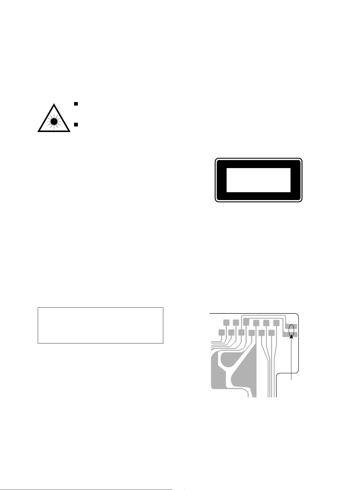
PROTECTION OF EYES FROM LASER BEAM DURING SERVICING
This set employs laser. Therefore, be sure to follow carefully the
instructions below when servicing.
WARNING!
WHEN SERVICING, DO NOT APPROACH THE LASER EXIT
WITH THE EYE TOO CLOSELY. IN CASE IT IS NECESSARY TO
CONFIRM LASER BEAM EMISSION. BE SURE TO OBSERVE
FROM A DISTANCE OF MORE THAN 30cm FROM THE
SURFACE OF THE OBJECTIVE LENS ON THE OPTICAL
PICK-UP BLOCK.
Caution: Invisible laser radiation when
open and interlocks defeated avoid exposure to beam.
Advarsel:Usynling laserståling ved åbning,
når sikkerhedsafbrydere er ude af funktion.
Undgå udsættelse for stråling.
VAROITUS!
Laiteen Käyttäminen muulla kuin tässä käyttöohjeessa mainitulla tavalla saattaa altistaa käyt-täjän turvallisuusluokan 1 ylittävälle näkymättömälle lasersäteilylle.
VARNING!
Om apparaten används på annat sätt än vad som specificeras i
denna bruksanvising, kan användaren utsättas för osynling
laserstrålning, som överskrider gränsen för laserklass 1.
CAUTION
Use of controls or adjustments or performance of procedures
other than those specified herein may result in hazardous
radiation exposure.
ATTENTION
L'utilisation de commandes, réglages ou procédures autres que
ceux spécifiés peut entraîner une dangereuse exposition aux
radiations.
ADVARSEL!
Usynlig laserståling ved åbning, når sikkerhedsafbrydereer ude
af funktion. Undgå udsættelse for stråling.
This Compact Disc player is classified as a CLASS 1 LASER
product.
The CLASS 1 LASER PRODUCT label is located on the rear
exterior.
CLASS 1
KLASSE 1
LUOKAN 1
KLASS 1
LASER PRODUCT
LASER PRODUKT
LASER LAITE
LASER APPARAT
Precaution to replace Optical block
(KSS – 213B)
Body or clothes electrostatic potential could ruin
laser diode in the optical block. Be sure ground
body and workbench, and use care the clothes
do not touch the diode.
1) After the connection, remove solder shown in
the right figure.
CD PICK-UP ASSY P.C.B.
Solder
3
Page 4

ELECTRICAL MAIN PARTS LIST
REF. NO PART NO. KANRI DESCRIPTION
IC
87-A20-459-010 C-IC,LC78622ED
8Z-CH4-636-010 IC,LC867132V-5K36
87-A21-184-010 IC,TA2104AN
87-A21-185-040 C-IC,LC72121M
87-A20-946-040 C-IC,MM1434XF
87-A20-591-010 IC,BA5417
87-A21-111-040 C-IC,M62495FP
87-070-416-010 IC,NJU7201 L55
87-A20-446-010 C-IC,LA9241ML
87-A21-093-010 IC,LA6541D
87-A21-145-040 C-IC,BA4560F-E2
TRANSISTOR
87-026-291-010 TR,DTC124XS
89-213-702-010 TR,2SB1370E(1.8W)
89-319-233-080 TR,2SC1923 (0.1W)
87-A30-092-080 FET,2SK439E/F
87-026-447-080 TR,2SC1740S R
89-320-011-080 TR,2SC2001K(15W)
87-026-214-080 TR,DTA114YS (0.3W)
87-026-215-010 TR,DTC114YS
89-112-965-010 TR,2SA1296GR
87-026-463-010 TR,2SA933S,RS
87-026-462-010 TR,2SC1740SRS
89-113-184-080 TR,2SA1318TU
89-112-965-080 TR,2SA1296GR(0.75W)
87-026-464-010 TR,DTC114TS
87-026-239-010 TR,DTC114TK
89-318-154-010 TR,2SC1815Y
89-318-155-010 TR,2SC1815(GR)
87-026-496-080 FET,2SJ103GR
88-NF9-637-010 TR,2SA1318T/U
89-110-150-010 TR,2SA1015
DIODE
87-070-345-080 DIODE,IN4148
87-017-072-080 ZENER,HZS3B1
87-027-607-080 ZENER,HZ7B3L
87-A40-466-080 ZENER,MTZJ2.7A
87-020-465-080 DIODE,1SS133 (110MA)
87-017-162-080 ZENER,HZS7C3L
87-017-148-080 ZENER,HZS6A1L
87-017-139-010 ZENER,HZS15-2
87-070-136-080 ZENER,MTZJ5.1B
87-A40-465-010 DIODE,FR202
MAIN C.B
C1 87-010-314-080 C-CAP,S 22P-50V
C2 87-010-316-080 C-CAP,S 33P-50 CH
C3 87-010-314-080 C-CAP,S 22P-50V
C5 87-A11-067-080 C-CAP,S 1-10 K B
C6 87-010-312-080 C-CAP,S 15P CH
C7 87-014-409-080 CAP,PP 470P-100J
C8 87-012-349-080 C-CAP,S 1000P-50 CH
C10 87-010-197-080 CAP, CHIP 0.01 DM
C11 87-010-197-080 CAP, CHIP 0.01 DM
C12 87-010-197-080 CAP, CHIP 0.01 DM
C13 87-010-150-080 C-CAP,S 6P-50 CH
C14 87-012-157-080 C-CAP 330P-50CH
C15 87-012-349-080 C-CAP,S 1000P-50 CH
C16 87-010-380-080 CAP, ELECT 47-16V
C17 87-010-198-080 CAP, CHIP 0.022
C18 87-015-819-080 CAPACITOR,0.01
C19 87-010-112-080 CAP, ELECT 100-16V
C20 87-010-404-080 CAP, ELECT 4.7-50V
C21 87-010-197-080 CAP, CHIP 0.01 DM
NO.
REF. NO PART NO. KANRI DESCRIPTION
C22 87-010-197-080 CAP, CHIP 0.01 DM
C24 87-012-157-080 C-CAP 330P-50CH
C25 87-016-460-080 C-CAP,S 0.22-16 B
C26 87-010-322-080 C-CAP,S 100P-50
C27 87-A11-067-080 C-CAP,S 1-10 K B
C28 87-016-669-080 C-CAP,S 0.1-25 K B
C29 87-016-669-080 C-CAP,S 0.1-25 K B
C30 87-010-220-080 C-CAP,S 0.018-25 KB
C31 87-010-220-080 C-CAP,S 0.018-25 KB
C33 87-010-401-080 CAP, ELECT 1-50V
C34 87-010-401-080 CAP, ELECT 1-50V
C35 87-015-819-080 CAPACITOR,0.01
C36 87-010-112-080 CAP, ELECT 100-16V
C37 87-010-197-080 CAP, CHIP 0.01 DM
C38 87-010-380-080 CAP, ELECT 47-16V
C39 87-010-404-080 CAP, ELECT 4.7-50V
C40 87-010-197-080 CAP, CHIP 0.01 DM
C41 87-012-349-080 C-CAP,S 1000P-50 CH
C42 87-012-349-080 C-CAP,S 1000P-50 CH
C43 87-012-349-080 C-CAP,S 1000P-50 CH
C44 87-010-311-080 C-CAP,S 12P-50 J CH GRM
C45 87-010-312-080 C-CAP,S 15P-50 CH
C46 87-010-197-080 CAP, CHIP 0.01 DM
C47 87-010-197-080 CAP, CHIP 0.01 DM
C48 87-010-197-080 CAP, CHIP 0.01 DM
C49 87-012-156-080 C-CAP,S 220P-50 CH
C50 87-010-197-080 CAP, CHIP 0.01 DM
C51 87-010-316-080 C-CAP,S 33P-50 CH
C52 87-010-197-080 CAP, CHIP 0.01 DM
C53 87-010-197-080 CAP, CHIP 0.01 DM
C54 87-014-055-080 CAP,PP 820P-100 J
C55 87-010-197-080 CAP, CHIP 0.01 DM
C71 87-010-197-080 CAP, CHIP 0.01 DM
C72 87-016-669-080 C-CAP,S 0.1-25 K B
C73 87-016-669-080 C-CAP,S 0.1-25 K B
C78 87-016-669-080 C-CAP,S 0.1-25 K B
C207 87-010-408-080 CAP, ELECT 47-50V
C208 87-010-402-080 CAP, ELECT 2.2-50V
C209 87-010-190-080 S CHIP F 0.01
C210 87-010-190-080 S CHIP F 0.01
C211 87-010-401-080 CAP, ELECT 1-50V
C212 87-010-401-080 CAP, ELECT 1-50V
C215 87-010-425-080 C-CAP,0.22-25 F
C216 87-010-425-080 C-CAP,0.22-25 F
C217 87-010-400-080 CAP, ELECT 0.47-50V
C218 87-010-400-080 CAP, ELECT 0.47-50V
C220 87-010-405-080 CAP, ELECT 10-50V
C222 87-010-190-080 S CHIP F 0.01
C223 87-010-190-080 S CHIP F 0.01
C226 87-010-190-080 S CHIP F 0.01
C228 87-010-401-080 CAP, ELECT 1-50V
C229 87-010-401-080 CAP, ELECT 1-50V
C231 87-010-213-080 C-CAP,S 0.015-50 B
C232 87-010-213-080 C-CAP,S 0.015-50 B
C233 87-010-546-080 CAP, ELECT 0.33-50V
C234 87-010-546-080 CAP, ELECT 0.33-50V
C235 87-010-544-080 CAP, ELECT 0.1-50V
C236 87-010-544-080 CAP, ELECT 0.1-50V
C237 87-010-260-080 CAP, ELECT 47-25V
C238 87-010-263-080 CAP, ELECT 100-10V
C241 87-010-405-080 CAP, ELECT 10-50V
C242 87-010-405-080 CAP, ELECT 10-50V
C243 87-010-405-080 CAP, ELECT 10-50V
C244 87-010-405-080 CAP, ELECT 10-50V
C245 87-010-405-080 CAP, ELECT 10-50V
C246 87-010-405-080 CAP, ELECT 10-50V
C247 87-010-404-080 CAP, ELECT 4.7-50V
C248 87-010-404-080 CAP, ELECT 4.7-50V
C261 87-010-402-080 CAP, ELECT 2.2-50V
C262 87-010-402-080 CAP, ELECT 2.2-50V
NO.
4
Page 5

REF. NO PART NO. KANRI DESCRIPTION
C263 87-010-178-080 CHIP CAP 1000P
C264 87-010-178-080 CHIP CAP 1000P
C265 87-010-383-080 CAP, ELECT 33-25V
C266 87-010-383-080 CAP, ELECT 33-25V
C267 87-010-380-080 CAP, ELECT 47-16V
C268 87-010-380-080 CAP, ELECT 47-16V
C271 87-010-236-080 CAP, ELECT 1000-10V
C272 87-010-236-080 CAP, ELECT 1000-10V
C275 87-010-628-080 CAP,E 3.3-16 M 5L BP SRE
C276 87-010-628-080 CAP,E 3.3-16 M 5L BP SRE
C277 87-010-260-080 CAP, ELECT 47-25V
C278 87-010-263-080 CAP, ELECT 100-10V
C279 87-010-112-080 CAP, ELECT 100-16V
C299 87-010-190-080 S CHIP F 0.01
C301 87-010-453-010 CAP, ELECT 4700-25V
C306 87-010-404-080 CAP, ELECT 4.7-50V
C307 87-010-401-080 CAP, ELECT 1-50V
C308 87-010-221-080 CAP, ELECT 470-10V
C309 87-010-263-080 CAP, ELECT 100-10V
C310 87-010-248-080 CAP, ELECT 220-10V
C311 87-010-384-080 CAP, ELECT 100-25V
C312 87-010-385-080 CAP, ELECT 220-25V
C314 87-010-248-080 CAP, ELECT 220-10V
C315 87-010-197-080 CAP, CHIP 0.01 DM
C321 87-010-190-080 S CHIP F 0.01
C322 87-010-263-080 CAP, ELECT 100-10V
C325 87-010-405-080 CAP, ELECT 10-50V
C341 87-010-197-080 CAP, CHIP 0.01 DM
C342 87-010-221-080 CAP, ELECT 470-10V
C343 87-010-401-080 CAP, ELECT 1-50V
C801 87-010-402-080 CAP, ELECT 2.2-50V
C802 87-010-402-080 CAP, ELECT 2.2-50V
C803 87-010-181-080 C-CAP,S 1800P-50 KB
C804 87-010-181-080 C-CAP,S 1800P-50 KB
C805 87-012-158-080 C-CAP,S 390P-50 CH
C806 87-012-158-080 C-CAP,S 390P-50 CH
C809 87-010-379-010 CAP,E 22-10 SM
C810 87-010-379-010 CAP,E 22-10 SM
C811 87-010-404-010 CONDENSER 4.7-50
C812 87-010-404-010 CONDENSER 4.7-50
C815 87-010-374-010 CAP, ELECT 47-10V
C816 87-010-384-080 CAP, ELECT 100-25V
C819 87-010-401-010 CAP, ELECT 1-50V
C820 87-010-401-010 CAP, ELECT 1-50V
C821 87-010-183-080 C-CAP,S 2700P-50 KB
C822 87-010-183-080 C-CAP,S 2700P-50 KB
C823 87-010-213-080 C-CAP,S 0.015-50 B
C824 87-010-213-080 C-CAP,S 0.015-50 B
C825 87-010-405-080 CAP, ELECT 10-50V
C826 87-010-405-080 CAP, ELECT 10-50V
C827 87-010-404-010 CONDENSER 4.7-50
C828 87-010-404-010 CONDENSER 4.7-50
C830 87-010-260-080 CAP, ELECT 47-25V
C831 87-010-198-080 CAP, CHIP 0.022
C832 87-010-198-080 CAP, CHIP 0.022
C833 87-010-179-080 CAP,CHIP S B1200P
C834 87-010-248-080 CAP, ELECT 220-10V
C835 87-012-358-010 C-CAP,S 0.47-16V
C837 87-010-374-010 CAP, ELECT 47-10V
C838 87-010-405-080 CAP, ELECT 10-50V
C841 87-010-182-080 C-CAP,S 2200P-50 KB
C842 87-010-182-080 C-CAP,S 2200P-50 KB
C843 87-010-190-080 S CHIP F 0.01
C844 87-018-128-080 CAP,TC U 560P-50 KB
C845 87-018-128-080 CAP,TC U 560P-50 KB
C846 87-010-194-080 CAP, CHIP 0.047
C849 87-010-177-080 CHIP CAPACITOR 820P
C850 87-010-177-080 CHIP CAPACITOR 820P
C851 87-010-186-080 CAP,CHIP 4700P
C852 87-010-178-080 CHIP CAP 1000P
NO.
REF. NO PART NO. KANRI DESCRIPTION
C853 87-010-190-080 S CHIP F 0.01
CF2 82-785-747-080 CF,MS2 GHY,R
CF3 82-785-747-080 CF,MS2 GHY,R
CF4 87-A91-094-010 FLTR,CDA10.7 MG
CN201 87-099-016-010 CONN,14P 6216V
CN203 87-049-469-010 CONN,4P V
CN204 87-049-469-010 CONN,4P V
CN205 87-A60-109-010 CONN,2P V S2M-2W
CN301 S1-2S3-002-500 CONN,3P
CN801 87-049-469-010 CONN,4P V
CN802 87-049-469-010 CONN,4P V
D3 87-A40-616-070 VARI-CAP,SVC384(S/T)
D4 87-A40-615-070 VARI-CAP,KV1311NT
D5 87-A40-615-070 VARI-CAP,KV1311NT
L2 87-A50-347-010 COIL,FM BPF EX
L3 87-A91-096-010 BAR-ANT,MW/LW FOR 3B(SYN)
L4 87-A50-420-010 COIL,MW OSC(SYN)
L5 87-A50-424-010 COIL,FM RF EX(SYN)
L6 87-A50-427-010 COIL,FM OSC EX(SYN)
L7 87-A91-308-010 FLTR,PCFAZH- 450T (TOK)
L8 87-005-849-080 COIL,10UH(CECS)
L9 87-005-849-080 COIL,10UH(CECS)
L51 87-A50-421-010 COIL,LW OSC(SYN)
L801 87-007-342-010 COIL,OSC 85K BIAS
R840 87-029-124-010 RES,FUSE 2.2-1/4
TC1 87-011-220-080 TRIMMER CAP 20P VTC
TC51 87-011-233-080 TRIMER,50P VCT54
X1 87-A70-061-010 VIB,XTAL 4.500MHZ CSA-309
FRONT C.B
C601 87-010-313-080 CAP, CHIP 18P
C602 87-010-315-080 C-CAP,S 27P-50 CH
C603 87-010-319-080 C-CAP,S 56P-50 J CH
C604 87-010-312-080 C-CAP,S 15P-50V CH
C605 87-010-317-080 C-CAP,S 39P-50 CH
C607 87-A11-067-080 C-CAP,S 1-10 K B
C608 87-A11-067-080 C-CAP,S 1-10 K B
C610 87-010-263-080 CAP, ELECT 100-10
C611 87-010-196-080 CHIP CAPACITOR,0.1-25
C612 87-010-248-080 CAP, ELECT 220-10V
C613 87-010-402-080 CAP, ELECT 2.2-50V
C614 87-010-196-080 CHIP CAPACITOR,0.1-25
C615 87-010-400-080 CAP, ELECT 0.47-50V
C616 87-010-401-080 CAP, ELECT 1-50V
C620 87-A11-067-080 C-CAP,S 1-10 K B
C627 87-010-401-080 CAP,E 1-50
C628 87-010-401-080 CAP,E 1-50
C691 87-010-405-080 CAP, ELECT 10-50V
CN601 87-099-031-010 CONN,14P 6216 H
CN602 87-099-200-010 CONN,7P 6216H
CN603 87-099-199-010 CONN,6P 6216 H
CN604 87-099-200-010 CONN,7P 6216H
CN605 87-099-200-010 CONN,7P 6216H
FC601 8Z-CH4-619-010 FF-CABLE, 14P AF-FR
FC602 8Z-CH4-621-010 FF-CABLE, 7P CD-FR
FC603 8Z-CH4-622-010 FF-CABLE, 6P TU-FR
FC604 8Z-CH4-620-010 FF-CABLE, 7P FR-LED
FC605 8Z-CH4-620-010 FF-CABLE, 7P FR-LED
L601 87-003-102-010 COIL,10UH TROIDAL
LCD601 8Z-CH4-635-010 LCD,HLC7365 ZCH-4
S601 87-A90-696-080 SW,TACT TS2103-03-430
S604 87-A90-696-080 SW,TACT TS2103-03-430
S605 87-A90-696-080 SW,TACT TS2103-03-430
S606 87-A90-696-080 SW,TACT TS2103-03-430
S607 87-A90-696-080 SW,TACT TS2103-03-430
S614 87-A90-696-080 SW,TACT TS2103-03-430
S615 87-A90-696-080 SW,TACT TS2103-03-430
X601 87-030-273-010 VIB,XTAL 32.768K5PPM
X602 87-A70-070-080 VIB,CER 5.76MHZ CRHF
NO.
5
Page 6

REF. NO PART NO. KANRI DESCRIPTION
NO.
CD MAIN C.B
C401 87-010-403-080 CAP, ELECT 3.3-50V
C402 87-010-197-080 CAP, CHIP 0.01 DM
C403 87-010-263-080 CAP, ELECT 100-10V
C404 87-010-248-080 CAP, ELECT 220-10V
C405 87-010-197-080 CAP, CHIP 0.01 DM
C406 87-010-374-080 CAP, ELECT 47-10V
C407 87-010-178-080 CHIP CAP 1000P
C409 87-010-248-080 CAP, ELECT 220-10V
C410 87-010-263-080 CAP, ELECT 100-10V
C412 87-010-401-080 CAP, ELECT 1-50V
C413 87-A11-138-080 CAP, CHIP 0.033-50
C414 87-010-405-080 CAP, ELECT 10-50V
C416 87-010-545-080 CAP, ELECT 0.22-50V
C417 87-012-157-080 C-CAP,S 330P-50 CH
C425 87-010-176-080 C-CAP,S 680P-50 SL
C429 87-010-186-080 CAP,CHIP 4700P
C430 87-012-156-080 C-CAP,S 220P-50 CH
C431 87-010-545-080 CAP, ELECT 0.22-50V
C432 87-010-374-080 CAP, ELECT 47-10V
C433 87-010-401-080 CAP, ELECT 1-50V
C434 87-010-184-080 CHIP CAPACITOR 3300P(K)
C435 87-010-197-080 CAP, CHIP 0.01 DM
C436 87-010-374-080 CAP, ELECT 47-10V
C437 87-010-404-080 CAP, ELECT 4.7-50V
C438 87-010-196-080 CHIP CAPACITOR,0.1-25
C440 87-010-145-080 C-CAP,S 1P-50 CH
C442 87-010-312-080 C-CAP,S 15P-50 CH
C445 87-010-196-080 CHIP CAPACITOR,0.1-25
C446 87-010-196-080 CHIP CAPACITOR,0.1-25
C447 87-010-196-080 CHIP CAPACITOR,0.1-25
C448 87-010-315-080 C-CAP,S 27P-50 CH
C450 87-012-140-080 CAP 470P
C451 87-012-156-080 C-CAP,S 220P-50 CH
C455 87-010-263-080 CAP, ELECT 100-10V
C457 87-010-312-080 C-CAP,S 15P-50 CH
C458 87-010-312-080 C-CAP,S 15P-50 CH
C459 87-010-263-080 CAP, ELECT 100-10V
C460 87-010-197-080 CAP, CHIP 0.01 DM
C461 87-010-196-080 CHIP CAPACITOR,0.1-25
C462 87-010-248-080 CAP,E 220-10 SME
C465 87-010-404-080 CAP, ELECT 4.7-50V
C466 87-010-196-080 CHIP CAPACITOR,0.1-25
C467 87-010-263-080 CAP, ELECT 100-10V
C469 87-012-154-080 C-CAP,S 150P-50 CH
C470 87-010-544-080 CAP, ELECT 0.1-50V
C475 87-010-197-080 CAP, CHIP 0.01 DM
C476 87-010-236-080 CAP,E 1000-10 SME
C477 87-010-197-080 CAP, CHIP 0.01 DM
C478 87-010-263-080 CAP, ELECT 100-10V
C479 87-010-197-080 CAP, CHIP 0.01 DM
C480 87-010-221-080 CAP, ELECT 470-10V
C481 87-010-405-080 CAP, ELECT 10-50V
C482 87-010-405-080 CAP, ELECT 10-50V
C483 87-012-156-080 C-CAP,S 220P-50 CH
C484 87-012-156-080 C-CAP,S 220P-50 CH
C489 87-010-196-080 CHIP CAPACITOR,0.1-25
C490 87-010-196-080 CHIP CAPACITOR,0.1-25
C491 87-010-197-080 CAP, CHIP 0.01 DM
C492 87-010-221-080 CAP, ELECT 470-10V
C493 87-010-197-080 CAP, CHIP 0.01 DM
C500 87-010-197-080 CAP, CHIP 0.01 DM
C501 87-010-196-080 CHIP CAPACITOR,0.1-25
C502 87-010-322-080 C-CAP,S 100P-50 CH
C503 87-010-322-080 C-CAP,S 100P-50 CH
C504 87-010-322-080 C-CAP,S 100P-50 CH
C505 87-010-322-080 C-CAP,S 100P-50 CH
C506 87-010-322-080 C-CAP,S 100P-50 CH
C510 87-010-196-080 CHIP CAPACITOR,0.1-25
REF. NO PART NO. KANRI DESCRIPTION
NO.
CN401 87-A60-424-010 CONN,16P V TOC-B
CN402 8Z-CH4-614-010 CONN ASSY,6P CD-ME
CN403 87-099-195-010 CONN,7P 6216 V
FC401 8Z-CH4-618-010 FF-CABLE, 16P CD-RF
L401 87-003-102-080 COIL, 10UH
L404 87-008-372-010 FILTER, EMI BL OIRNI
SFR430 87-024-176-080 SFR,100K H NVZ6TLTA
X401 81-592-641-010 CERAMIC FILTER, 16.93MHZ
LED C.B
CN608 87-099-200-010 CONN,7P 6216H
CN609 87-099-200-010 CONN,7P 6216H
LED601 88-CD6-630-010 LED,934ID RED
LED602 88-CD6-630-010 LED,934ID RED
LED603 88-CD6-630-010 LED,934ID RED
LED604 88-CD6-630-010 LED,934ID RED
LED606 88-CD6-630-010 LED,934ID RED
LED607 88-CD6-630-010 LED,934ID RED
LED608 88-CD6-630-010 LED,934ID RED
LED609 88-CD6-630-010 LED,934ID RED
LED610 88-CD6-631-010 LED,934GD GRN
KEY C.B
S608 87-A90-696-080 SW,TACT TS2103-03-430
S609 87-A90-696-080 SW,TACT TS2103-03-430
S610 87-A90-696-080 SW,TACT TS2103-03-430
S611 87-A90-696-080 SW,TACT TS2103-03-430
S612 87-A90-696-080 SW,TACT TS2103-03-430
S613 87-A90-696-080 SW,TACT TS2103-03-430
HP C.B
J251 87-A60-569-010 JACK,HTJ-035-18
PWR C.B
C901 87-A10-577-080 CAP,CER 0.022-50 Z YF
C902 87-A10-577-080 CAP,CER 0.022-50 Z YF
C903 87-A10-577-080 CAP,CER 0.022-50 Z YF
C904 87-A10-577-080 CAP,CER 0.022-50 Z YF
!F901 87-035-347-010 FUSE,2.5AL 250V T
!FC901 87-033-213-010 CLAMP,FUSE SMK
!FC902 87-033-213-010 CLAMP,FUSE SMK
MOTOR-1 C.B
M2 9X-262-576-910 MOTOR
PIN3 91-564-722-110 CONNECTOR 6P
SW1 91-572-085-120 LEAF SWITCH
6
Page 7
CHIP RESISTOR PART CODE
Chip Resistor Part Coding
88
LCD DISPLAY
A
Resistor Code
Chip resistor
Wattage Type Tolerance
1/16W 1005 5% CJ
1/16W
1/10W
1/8W
1608
2125
3216
5%
5%
5%
TRANSISTOR ILLUSTRATION
Symbol
CJ
CJ
CJ
Figure
Value of resistor
Form
L
Dimensions (mm)
t
W
0.55
Resistor Code
108
118
128
LW t
1.0 0.5 0.35 104
1.6 0.8 0.45
2 1.25 0.45
3.2
1.6
: A
: A
E C B
2SA1015
2SA1296
2SA1318
2SC1815
2SC1923
2SC2001
2SC2878
S G D
2SJ103
E C B
2SA933S
2SC1740S
DTA114YS
DTC114TK
DTC114TS
DTC114YS
DTC124XS
G S D
2SK439
B C E
2SB1370
87
Page 8
WIRING-1
1
A
B
C
D
234567
8
9
10
11 12 13
14
E
F
G
H
I
J
109
Page 9
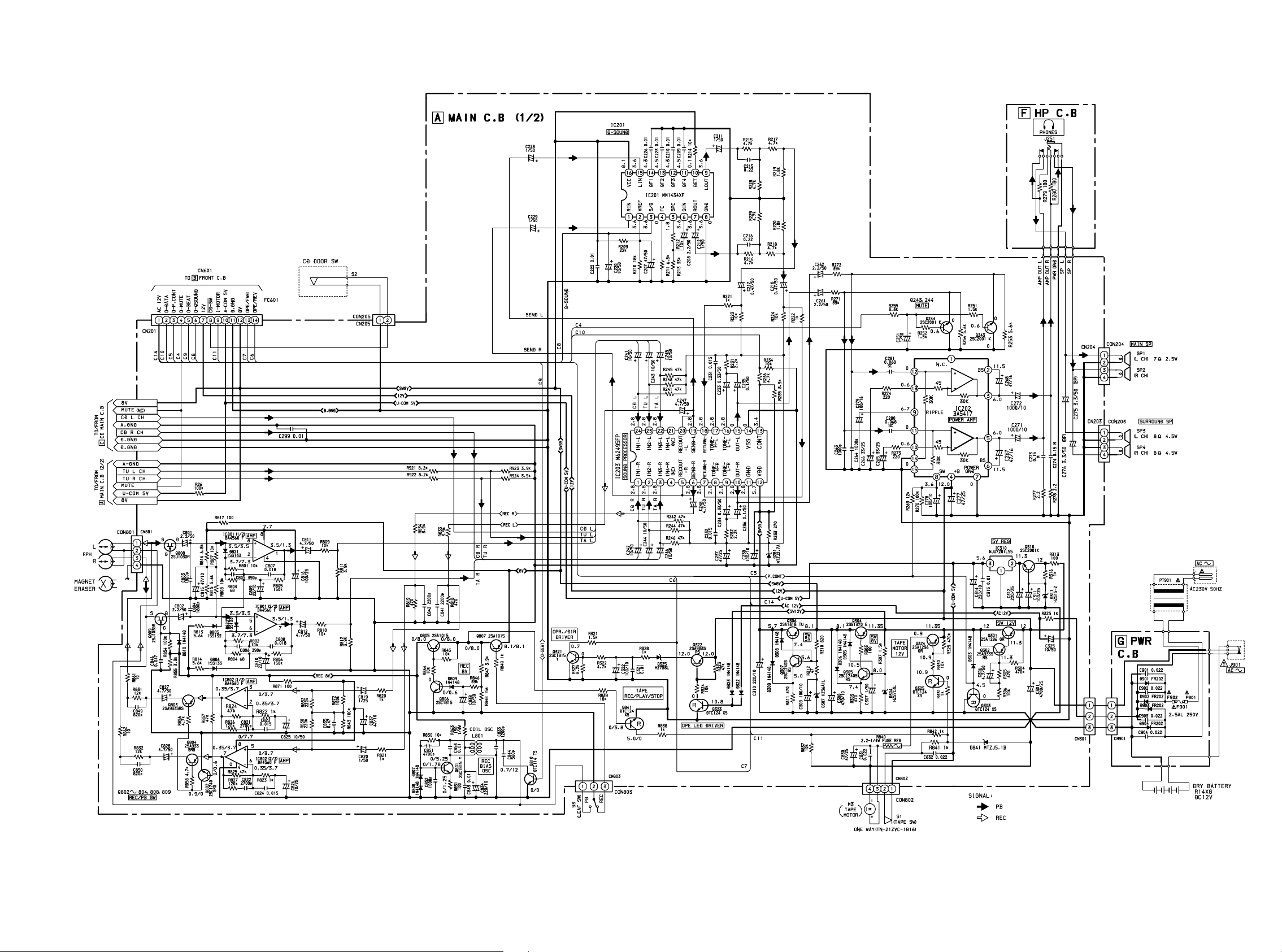
SCHEMATIC DIAGRAM-1 (MAIN-1/2 SECTION)
1/4W
1/4W
1211
Page 10

SCHEMATIC DIAGRAM-2 (MAIN 2/2 SECTION)
1413
Page 11

SCHEMATIC DIAGRAM-3 (CD MAIN SECTION)
1615
Page 12

WIRING-2
1
A
B
C
D
234567
8
9
10
11 12 13
14
E
F
G
H
I
J
1817
Page 13

SCHEMATIC DIAGRAM-3 (FRONT, LED, KEY SECTION)
2019
Page 14

ADJUSTMENT <TUNER / CD>
3
L003 (BAR ANT)
A
MAIN C.B
2
L004
L005
TC001
IC001
1
L006
IC002
L007
4
3
5
C
CD MAIN C.B
IC402
IC404
SFR430
TP1 (RF)
IC401
TP2 (VREF)
PRACTICAL SERVICE FIGURE
<TUNER SECTION>
<FM SECTION>
IHF Sensitivity : Less than 18dB
6
6
(THD 3%) [at 87.5 / 98 / 108MHz]
Signal to noise ratio : Mono : More than 66dB
Stereo : More than 58dB
[at 98MHz ]
Distortion : Less than 3% [at 98MHz ]
Auto stop level : 24dB ± 10dB
[at 87.5 / 98 / 108MHz]
Stereo separation : More than 20dB [at 98MHz]
Intermediate frequency : 10.7MHz
<AM(MW) SECTION>
Sensitivity : Less than 48dB
S/N (10dB) [at 600kHz]
Less than 46dB
[at 1000kHz]
Less than 44dB
[at 1400kHz]
Signal to noise ratio : More than 30dB
[at 600 / 1000 / 1400kHz]
Distortion : Less than 3%
[at 1000kHz]
Auto stop level : Less than 70dB
[at 600kHz]
Less than 65dB
[at 1000kHz]
Less than 60dB
[at 1400kHz]
Intermediate frequency : 450kHz
<DECK SECTION>
Tape speed : 3000Hz +90 / -60Hz (TN-21ZVC-1816)
3000Hz ± 90Hz (TN-51RV-240)
Wow & flutter : Less than 0.4% (R.M.S)
Take-up torque : 30 ~ 60g-cm (FWD) (TN-21ZVC-1816)
20 ~ 60g-cm (FWD) (TN-51RV-240)
F.F & REW torque : 55 ~ 140g-cm (TN-21ZVC-1816)
55 ~ 120g-cm (TN-51RV-240)
Distortion : Less than 3% (PB, 1kHz, DC)
Less than 5% (REC/PB, 1kHz, DC)
S/N ratio : More than 35dB (PB, AC, DC)
More than 25dB (REC/PB, AC, DC)
Max Noise level : Less than 45mV (PB, DC, AC, VOL
MAX)
Min Noise level : Less than 1mV (PB, DC, VOL MIN)
Less than 1.2mV (PB, AC, VOL MIN)
Erasing ratio : More than 45dB
Test tape : TTA–100
TTA–210
TTA–782
TTA–602 (NORMAL)
< TUNER SECTION >
1. AM (MW) IF Adjustment
L007 .............................................................................. 450 kHz
2. AM (MW) VT Adjustment
Settings : • Test point : TP3
• Adjustment location : L004
Method : Set to AM (MW) 1710kHz (HA, LH), 1602kHz (HR)
1611kHz (EZ) and adjust L004 so that the test point
is 6.0 ± 0.05V (HA, LH), 5.6 ± 0.05V (HR, EZ).
3. AM (MW) Tracking Adjustment
L003 .................................. 600kHz (HA, LH), 603kHz (HR, EZ)
TC001 ............................ 1400kHz (HA, LH), 1404kHz (HR, EZ)
4. FM VT Adjustment
Settings : • Test point : TP3
• Adjustment location : L006
Method : Set to FM 108MHz and adjust L006 so that the test
point is 6.0 ± 0.05V.
5. FM Tracking Adjustment
L005 ............................................................................. 108MHz
6. LW VT Adjustment<EZ>
Settings : • Test point : TP3
• Adjustment location : L051
Method : Set to LW 288kHz and adjust L051 so that the test
point is 4.5 ± 0.05V.
7. LW Tracking Adjustment<EZ>
L003 ............................................................................... 153kHz
TC051 ............................................................................ 288kHz
< CD SECTION >
8. Focus Bias Adjustment
Make the focus bias adjustment when replacing and repairing
the optical block.
TP3 (RF)
TP2 (VREF)
1) Connect an oscilloscope to the test points TP1 (RF) and TP2
(VREF).
2) Turn on the power switch.
3) Insert test disc TCD-782 (YEDS-18) and play back the
second composition.
4) Adjust SFR430 so that RF signal of the test point TP1 (RF)
is MAX and CLEAREST.
RF signal waveform
EYE PATTERN
Must be CLEAR and MAX
Oscilloscope
(DC range)
+
-
VOLT / DIV: 50mV
TIME / DIV: 0.5µs
<LW SECTION> (EZ)
Sensitivity : Less than 60dB [at 153kHz]
(S/N 10dB) Less than 58dB at [198kHz]
Less than 56dB [at 288kHz]
Signal to noise ratio : More than 30dB
[at 153 / 198 / 288kHz]
Distortion : Less than 3% [at 198MHz ]
Auto stop level : Less than 80 / 75 / 70dB
[at 153 / 198 / 288kHz]
Intermediate frequency : 450kHz
MAX
2221
Page 15

IC BLOCK DIAGRAM
IC, LA6541D
IC, LC72121M
23
Page 16

IC, M62495FP IC, MM1434XF
IC, T A2104AN
24
Page 17

IC DESCRIPTION
IC, LC867132V-5K36
Pin No. Pin Name I/O Description
CD read/write control output and TU CE.
1
2
3
4
5
6
7
8
9
10
11
12
13
14
15
16
17
18
19
20
21
22
23
24
25
26
27
28
29
30
31
32
33
34
35
36
37~40
41
42
43~50
51~54
55
O-RMC/CE
O-DATA
O-CLK
NC
O-CK SFT
I-HOLD
I-RST
XT1 (IN)
XT2 (OUT)
VSS1
CF1 (IN)
CF2 (OUT)
VDD1
I-FM ST
I-KEYO
I-CD SW
I-KEY1
I-MOTOR
I-REC
I-FM/AM (NC)
I-TU DO
O-BASS LED
O-QS LED
O-DUBB LED (NC)
O-INT
I-DRF
I-WRQ
I-REMO
SO-PAO
S1/PA1
S2/PA2
S3/PA3
S4/PA4
S5/PA5
S6/PA6
S7/PA7
S8~S11
VDD3
VSS3
S12~S19
S20~S23 (NC)
O-CD LED
O
Data output to LC72121M, M62495FP.
O
Output LC72121M CLK.
O
Not Connected.
–
Clock shift output of the microcomputer.
O
Hold status detection.
I
Microcomputer reset.
I
I
Connected to 32.768KHZ crystal oscillator.
O
GND.
–
I
Connected to 6MHZ Ceramic Filter.
O
Power supply for microcomputer (+5V).
—
FM STEREO status input.
I
KEY AD input.
I
CD DOOR SW status detection input.
I
KEY AD input.
I
DECK MECHA MOTOR status input.
I
REC status input.
I
FM, AM status input. (Not connected)
I
Data input from LC72121M.
I
BASS LED ON/OFF control output.
O
Q-Sound LED ON/OFF control output.
O
LED control output used for high-speed dubbing. (Not connected)
O
INT DIODE MATRIX detection output.
O
CD RF level detection input.
I
CD sub-code Q standby input.
I
Remote control input.
I
LCD segment output and initial settings output. (SW)
O
LCD segment output and initial settings output. (LW)
O
LCD segment output and initial settings output. (MW 10K)
O
LCD segment output and initial settings output. (FM WIDE)
O
LCD segment output and initial settings output. (OIRT)
O
LCD segment output and initial settings output. (SW2)
O
LCD segment output and initial settings output. (ZCH)
O
O
LCD segment output and initial settings output.
O
Power supply for microcomputer (+5V).
—
GND.
—
LCD segment output.
O
LCD segment output. (Not Connected)
O
LED ON/OFF control output for CD functions.
O
25
Page 18

Pin No. Pin Name I/O Description
56
57
58
59
60
61
62
63
64~66
67
68
69
70
71
72
73
74
75
76
77
78
79
80
O-TU LED
O-TA LED (NC)
O-ROCK LED
O-POP LED
O-JAZZ LED
NC
I-CD TEST (NC)
I-TU TEST (NC)
COM0~COM2
NC
VSS2
VDD2
O-CD ON
O-TU ON
O-P.CONT
O-HI DUBB (NC)
O-MUTE
O-FM MONO (NC)
O-BEAT CONT
O-QSOUND
O-COIN
I-SQOUT
O-CQCK
LED ON/OFF control output for TU functions.
O
LED ON/OFF control output for TAPE functions. (Not Connected)
O
O
LED ON/OFF control output for ROCK.
LED ON/OFF control output for POP.
O
LED ON/OFF control output for JAZZ.
O
–
Not connected.
I
I
O
LCD common output.
Not connected.
–
GND.
–
–
Power supply for microcomputer (+5V).
CD PWR control output.
O
TU PWR control output.
O
O
Power supply control output.
Dubbing speed control output. (Not connected)
O
Main mute output.
O
O
FM force control MONO output. (Not connected)
BEAT switch over output.
O
Q-Sound ON/OFF output.
O
O
CD command output.
CD sub-code Q input.
I
CLK for CD commands/sub-codes.
O
26
Page 19

IC, LC78622ED
Pin No. Pin Name I/O Description
1 DEFI I Defect detection signal (DEF) input terminal.
2 TAI I A pull-down resistor is built in. (Connected to 0V)
3 PDO O External VCO control phase comparator output.
4 VVSS – Connected to internal VCO of PLL. (Connected to 0V)
5 ISET I PDO output current adjustment resistor connection.
6 VVDD – Voltage terminal for internal VCO of PLL.
7 FR I VCO frequency range adjustment.
8 VSS – Digital system ground. (Connected to 0V)
9 EFMO O EFM signal output pin.
10 EFMIN I EFM signal input pin.
11 T2 I Test pin. (Connected to 0V)
12 CLV+
13 CLV–
O Disc motor control output.
14 V/P O
15 HFL I Track detection signal input.
16 TES I Tracking error signal input.
17 TOFF O Tracking off output.
18 TGL O Tracking gain switching output.
19 JP+
O Track jump output.
20 JP–
21 PCK O EFM data playback monitor. Outputs 4.3218MHz when the phase is locked. (Not used)
22 FSEQ O signal detected from EFM signal and internally generated synchronization signal
23 VDD – Digital system power supply.
24 SL+
O Serial data command sled signal output terminal from microprocessor.
25 SL–
26 NC – Not used.
27 PU IN I CD pickup inside limit switch. (Not used)
28 NC – Not used.
Rough servo/phase control automatic switching monitor output.
Rough servo at "H". Phase control at "L".
Synchronization signal detection output. Outputs a "H" level when the synchronization
range.(Not used)
29 EMPH O
30 C2F O C2 flag output. (Not used)
31 DOUT O Digital output (EIAJ format). (Not used)
32 T3 I Test input. (Connected to 0V)
33 T4 I Test input. (Connected to 0V)
34 NC – Not used.
35 MUTEL O Left channel mute output. (Not used)
36 LVDD – Left channel power supply.
37 LCHO O Left channel output.
De-emphasis monitor pin. A "H" level indicates playback of a de-emphasis disc.
(Not used)
27
Page 20

Pin No. Pin Name I/O Description
38 LVSS – Left channel ground.
39 RVSS – Right channel ground.
40 RCHO O Right channel output.
41 RVDD – Right channel power supply.
42 MUTER O Right channel mute output. (Not used)
43 XVDD – Crystal oscillator power supply.
44 XOUT O
45 XIN I
46 XVSS – Crystal oscillator ground.
47 SBSY O Subcode block synchronization signal. (Not used)
48 EFLG O C1, C2 single and double error correction monitor pin. (Not used)
49 PW O Subcode P,Q,R,S,T,U and W output. (Not used)
50 SFSY O Subcode frame synchronization signal output. (Not used)
51 SBCK I Subcode readout clock input. (Connected to 0V)
52 FSX O
53 WRQ O Subcode Q output standby output.
54 RWC I Read/Write control input.
55 SQOUT O Subcode Q output.
56 COIN I Command input from the control microprocessor.
57 CQCK I Input for command input acquisition clock and SQOUT pin subcode readout clock.
58 RES I Chip reset input.
59 T11 O Test output. Leave open. (Not used)
60 16M O 16.9344MHz output. (Not used)
Connections for a 16.9344MHz crystal oscillator element.
Output for the 7.35kHz synchronization signal divided from the crystal oscillator.
(Not used)
61 4.2M O 4.2336MHz output.
62 T5 I Test input. (Connected to 0V)
63 CS I Chip select input. (Connected to 0V)
64 T1 I Test input. (Connected to 0V)
28
Page 21

IC, LA9241ML
Pin No. Pin Name I/O Description
1 FIN2 I
2 FIN1 I Connected to pickup photo-diode.
3 E I Connected to pickup photo-diode. Subtracting from F pin generates TE signal.
4 F I Connected to pickup photo-diode.
5 TB I Input DC components of TE signal.
6 TE– O Connected to TE pin with resistor set TE signal gain.
7 TE O Output TE signal.
8 TESI I Input TES (TRACK ERROR SENSE) comparator. Band pass and input TE signal.
9 SCI I Input shock detection.
10 TH I Establish tracking gain value.
11 TA O TA amplifier output.
12 TD– I Compose tracking phase compensation value between TD and VR pins.
13 TD O Used for tracking phase compensation setting.
14 JP I Establish amplitude of tracking jump signal (kick pulse).
15 TO O Output tracking control signal.
16 FD O Output focusing control signal.
17 FD– I Compose focusing phase compensation value between FD and FA pins.
Connected to pickup photo-diode. Adding with FIN1 pin generates RF signal, and
subtracting from FIN1 generates FE signal.
Pin No. Pin Name I/O Description
41 RFSM O Output RF.
42 RFS– O Establish RF gain and 3T compensation value from EFM signal with RFSM pin.
43 SLC O SLICE LEVEL CONTROL: Control data slice level by DSP with RF waveform.
44 SLI I Control data slice level by DSP.
45 DGND – Digital GND.
46 FSC O Connected to focus search smoothing capacitor.
47 TBC I TRACKING BALANCE CONTROL: Establish EF balance variable range.
48 NC – Not used.
49 DEF O Output disc defect detection.
50 CLK I Input reference clock. Inputs 4.23MHz from DSP.
51 CL I Input microcomputer command clock.
52 DAT I Input microcomputer command data.
53 CE I Input microcomputer command chip enable.
54 DRF O Detect RF: Output RF level detection.
55 FSS I
56 VCC2 – Servo/digital VCC.
57 REF1 – Connected to reference voltage bypass condenser.
FOCUS SEARCH SELECT: Switches focus search mode (between ± search
and + search against reference voltage). (Not used)
18 FA O Compose focusing phase compensation value between FD– and FA– pins.
19 FA– I Compose focusing phase compensation value between FA and FE pins.
20 FE O Output FE signal.
21 FE– I Connected to FE pin with resistor set FE signal gain.
22 AGND – Analog GND.
23 SP O Output single-end for CV+ and CV– pins input signal.
24 SPI I Spindle amplifier input.
25 SPG I Connect resistor for gain setting at spindle 12cm mode. (Not used)
26 SP– I Connect spindle phase compensation value with SPD pin.
27 SPD O Output spindle control signal.
28 SLEQ I Connect sled phase compensation value.
29 SLD O Output sled control signal.
30 SL–
I Input sled sending signal from DSP.
31 SL+
32 JP–
I Input tracking jump signal from DSP.
33 JP+
34 TGL I Input tracking gain control signal from DSP. TGL = "H" : Gain low.
35 TOFF I Input tracking off control signal from DSP. TOFF = "H" : Off.
58 VR O Output reference voltage.
59 LF2 – Establish value in detecting disc defect.
60 PHI – Connected to capacitor used to hold peak of RF signal.
61 BHI – Connected to capacitor used to hold bottom of RF signal.
62 LDD O APC-circuit output pin.
63 LDS I APC-circuit input pin.
64 VCC1 – RF VCC.
36 TES O Output TES signal to DSP.
37 HFL O HIGH FREQUENCY LEVEL: Detects whether main-beam is on pit or mirror position.
38 SLOF I Input sled servo off control.
39 CV–
I Input CLV error signal from DSP.
40 CV+
29
30
Page 22

MECHANICAL EXPLODED VIEW 1/1
19
26
18
43
LCD
42
12
11
14
DISP C.B
B
B
23
K
62
K
60
I
11
12
28
40
47
39
61
K
27
41
25
K
H
24
F
L
32
F
F
KSM213CDM
37
36
35
59
F
30
34
B
33
38
31
E
55
I
I
66
48
56
44
54
BATT C.B
58
67
7
F
B
J
P.C. B
F
P.C. B
57
49
8
B
48
A
45
A
C
B
C
63
P.C. B
F
46
53
6
50
51
52
D
A
A
TACT C.B
20
21
22
15
68
9
64
10
K
K
K
F
10
5
13
17
16
LED C.B
B
TN-21ZVC-1816
65
4
3
1
2
6
10
9
10
K
K
K
K
10
K
MAIN C.B
K
29
3231
Page 23

MECHANICAL PARTS LIST 1/1
REF. NO PART NO. KANRI DESCRIPTION
1 87-B00-020-010 BADGE,AIWA 30 GOLD
2 8Z-CH4-007-010 WINDOW,CASS
3 8Z-CH4-006-010 BOX,CASS
4 8Z-CH4-205-010 SPR-T,CASS
5 8Z-CH4-061-010 CABI,FR A
6 86-CT4-218-010 CUSHION,FOOT/PORON
7 8Z-CH4-019-010 CABI,TOP 2L
8 8Z-CH4-020-010 CABI,TOP 2R
9 88-CD5-603-010 SPKR,10 7OHM
10 8Z-CH4-204-010 HLDR,SPEAKER
11 84-CD5-215-010 GEAR
12 84-CD5-216-010 BRACKET
13 8Z-CH4-216-010 HLDR,FUNC-PWB
14 8Z-CH4-201-010 HLDR,LCD
15 8Z-CH4-016-010 WINDOW,LED
16 8Z-CH4-210-010 HLDR,LED
17 8Z-CH4-027-010 BTN,EQ
18 8Z-CH4-026-010 BTN,FUNC
19 8Z-CH4-025-010 BTN,REPEAT
20 8Z-CH4-064-010 WINDOW,LCD EZ
21 8Z-CH4-023-010 BTN,VOL
22 8Z-CH4-013-010 PANEL,LCD21
23 8Z-CH4-028-010 KEY,CASS 21
24 8Z-CH4-214-010 HLDR,REC-SW 21
25 87-A91-151-010 SW,LEAF 1P2T/TC48-021
26 8Z-CH4-024-010 BTN,CD
27 88-CH6-019-010 PANEL,CD
28 87-036-389-010 SW,PUSH LOCK
29 8Z-CH4-208-010 HLDR,PWB
30 8Z-CH4-030-010 COVER, PH
31 8Z-CH4-003-010 CHAS,CD
32 8Z-CH4-207-010 HLDR,OIL-DMPR
33 8Z-CH4-212-010 RING,CHUCK
34 8Z-CH4-211-010 BASE,CHUCK
35 87-036-368-010 MAGNET
36 84-CD5-217-010 PLATE,MAGNET
37 85-CD7-217-010 HLDR,CHUCK A
38 8Z-CH4-206-010 SPR-T,CD
39 8Z-CH4-004-010 BOX,CD
40 8Z-CH4-005-010 WINDOW,CD
41 8Z-CH4-213-010 SPR-P,REC-SW 21
42 8Z-CH4-622-010 FF-CABLE, 6P TU-FR
43 8Z-CH4-627-010 FF-CABLE, 7P FR-LED2
44 87-A90-086-010 COVER,AC-SOCKET
NO.
REF. NO PART NO. KANRI DESCRIPTION
45 87-CD6-041-010 PLATE,AC
46 8Z-CH4-640-010 ANT,ROD
47 8Z-CH4-009-010 HANDL,ARM
48 8Z-CH4-645-010 SPKR,MAYLOR 8OHM SILVER
49 8Z-CH4-010-010 HANDL,GRIP
50 8Z-CH4-008-010 LID,BATT
51 87-CD6-223-010 SPR-C,BATT LINK L
52 87-CD6-214-010 SPR-C,BATT LINK
53 8Z-CH4-002-010 CABI,REAR
! 54 88-CH6-627-010 PT,E
55 8Z-CH4-209-010 HLDR,PT
! 56 87-A60-178-010 JACK,AC E W/SW
57 87-CD6-222-010 SPR-C,BATT (-) L
58 87-CD6-213-010 SPR-C,BATT (-)
59 8Z-CH4-614-010 CONN ASSY,6P CD-ME
60 8Z-CH4-618-010 FF-CABLE, 16P CD-RF
61 8Z-CH4-621-010 FF-CABLE, 7P CD-FR
62 8Z-CH4-619-010 FF-CABLE, 14P AF-FR
63 88-CH6-207-010 HLDR,ANT
64 8Z-CH4-011-010 GRILLE,FR L
65 8Z-CH4-012-010 GRILLE,FR R
66 8Z-CH4-021-010 GRILLE,TOP L
67 8Z-CH4-022-010 GRILLE,TOP R
68 8Z-CH4-626-010 FF-CABLE, 7P FR-LED1
A 87-B10-242-010 UT2+3-30 W/O CR
B 87-B10-239-010 QT2+3-8 W/O CR
C 87-644-096-410 UT1+3-10 CR
D 87-254-097-410 U+3-12 CR
E 87-751-075-410 VT2+2.6-10
F 87-342-074-010 UT2+2.6-8
G 87-751-094-410 VT2+3-6 W10SL0T
H 87-261-037-410 V+2-10 GLD
I 87-661-100-410 VFT1+3-16
J 87-067-566-010 TAPPING SCREW, VFTT+3-6
K 87-741-095-410 UT2+3-8 GLD
L 87-571-032-410 VIT+2-3
NO.
COLOR NAME TABLE
Basic color symbol Color Basic color symbol Color Basic color symbol Color
B Black C Cream D Orange
G Green H Gray L Blue
LT Transparent Blue N Gold P Pink
R Red S Silver ST Titan Silver
T Brown V Violet W White
WT Transparent White Y Yellow YT Transparent Yellow
LM Metallic Blue LL Light Blue GT Transparent Green
LD Dark Blue DT Transparent Orange
33
Page 24

TAPE MECHANISM EXPLODED VIEW 1/1
F
G
1
E
2
R
8
10
J
L
14
b
18
19
51
36
46
47
55
9
53
20
21
22
23
24
LUG PLATE
52
4
3
a
15
16
17
34
35
11
5
12
13
49
M
6
7
31
30
A
32
33
26
25
A
27
28
29
56
N
54
C
N
37
38
39
42
43
48
b
a
c
C
B
B
B
D
D
K
41
N
40
I
50
45
57
c
N
44
34
Page 25

TAPE MECHANISM PARTS LIST 1/1
REF. NO PART NO. KANRI DESCRIPTION
1 S1-921-030-4A0 HEAD BASE
2 S1-821-030-070 AZIMUTH SPRING
3 S1-921-030-090 PANEL P SPRING
4 S1-921-260-050 GEAR PLATE SPRING
5 S1-921-265-020 GEAR PLATE ASSY
6 S1-921-140-370 P ARM COLLER
7 S1-921-140-340 P ARM
8 S1-921-030-110 HEAD PANEL
9 S1-921-143-160 BASE ASSY
10 S1-921-141-8A0 M CONTROL SPRING
11 S1-921-260-4A0 SENSING LEVER
12 S1-921-043-100 PINCH ROLLER ARM ASSY
13 S1-921-130-010 EJECT SLIDE LEVER
14 S1-921-141-3A0 P CONTROL SPRING
15 S1-921-140-550 PAUSE LEVER(E)
16 S1-921-140-120 PAUSE LEVER SPRING
17 S1-921-140-110 PAUSE STOPPER
18 S1-921-140-150 BUTTON LEVER SPRING(B)
19 S1-821-011-590 E KICK LEVER
20 S1-921-140-140 BUTTON LEVER SPRING(A)
21 S1-921-140-200 PR STOPPER
22 S1-921-140-090 SWITCH ACTUATOR
23 S1-921-140-080 PUSH BUTTON ACTUATOR
24 S1-921-140-190 PLAY BUTTON LEVER
25 S1-510-020-020 REC SPRING PLATE
26 S1-921-140-040 REW BUTTON LEVER
27 S1-921-140-050 FF,BUTTON REVER
28 S1-921-140-060 STOP BUTTON LEVER
29 S1-921-140-600 PAUSE BUTTON LEVER
30 S1-821-100-700 FF GEAR
31 S1-921-050-060 SENSOR
32 S1-921-053-030 TAKE UP REEL ASSY
33 S1-821-100-980 PACK SPRING
34 S1-921-053-040 SUPPLY REEL ASSY
35 S1-821-100-990 BACK TENSION SPRING
36 S1-921-140-030 REC BUTTON LEVER
37 S1-921-140-170 P.S.LEVER SPRING
38 S1-921-073-040 RF CLUTCH ASSY
39 S1-921-070-030 RF BELT
40 S1-921-260-020 CAM GEAR
NO.
REF. NO PART NO. KANRI DESCRIPTION
41 S1-921-140-160 E ACTUATOR SPRING
42 S1-921-093-030 FLYWHEEL ASSY
43 S1-921-090-040 MAIN BBELT
44 S1-921-120-010 MOTOR PULLEY
45 S6-002-030-220 MOTOR EG530AD-2B
46 S6-209-100-100 E HEAD PH-K380-MS1
47 S1-921-030-050 MG ARM
48 S1-921-140-210 REC BUTTON LEVER SPRING
49 S1-821-100-690 RECORD SAFETY LEVER
50 S1-921-120-540 MOTOR BRACKET
51 S1-821-010-500 PLAY BUTTON LEVER SPRING
52 S6-202-010-920 R.P HEAD MS15R-AK0N1
53 S6-401-011-490 LEAF SW MSW-1541T
54 S1-921-015-010 CHASSIS ASSY
55 S1-921-030-100 MG ARM SPRING
56 S1-921-010-160 SIDE BRACKET
57 S1-821-120-660 MOTOR RUBBER
A S9-P04-200-310 C TAPPING SCREW 2-3
B S1-851-140-180 MOTOR COLLER SCREW
C S9-B10-200-510 P TAPPING BIND SCREW M2-5
D S9-C07-204-510 SCREW,TAPPING(CAMERA)M2-4.5
E S9-P01-200-610 SCREW,M2-6
F S9-P01-200-310 SCREW,M2-3
G S9-F08-200-710 AZIMUTH SCREW M2-7
H S9-P05-200-810 S TAPPING SCREW M2-8
I S9-W02-300-100 P WASHER CUT 1.2-3.8-0.3
J S9-W02-500-100 P WASHER CUT 1.45-3.8-0.5
K S9-W01-400-100 P WASHER 2-3.5-0.4
L S9-W01-130-200 P WASHER 2.1-4-0.13
M S9-P08-203-010 PS TAPPING SCREW M2-3
N S9-P04-200-410 C TAPPING SCREW M2-4
NO.
35
Page 26

CD MECHANISM EXPLODED VIEW
2
COVER
GEAR
3
SPINDLE MOTOR
(M1)
4
CD MECHANISM PARTS LIST 1/1
REF. NO PART NO. KANRI DESCRIPTION
NO.
1 9X-262-620-210 MOTOR CHASSIS ASSY
2 92-626-907-010 GEAR(A)
3 87-A90-468-010 PICK UP KSS-213C
4 92-626-908-010 SHAFT SLED
A 97-621-255-150 SCREW+P2-3
A
1
MOTOR C.B
36
Page 27

2–1 1, IKENOHATA 1–CHOME, TAITO-KU, TOKYO 1 10, JAPAN TEL:03 (3827) 3111
931196
Printed in Singapore
 Loading...