

Page 1

CSD-A500
SERVICE MANUAL
Ver 1.1 2004. 09
Section
Section
Model Name Using Similar Mechanism CSD-A300
CD
CD Mechanism Type KSM-213RDP
Optical Pick-up Name KSS-213R
Model Name Using Similar Mechanism NEW
TC
Tape Transport Mechanism T ype MF-A500
E Model
CD player section
System
Compact disc digital audio system
Laser diode properties
Material: GaAlAs
Wave length: 780 nm
Emission duration: Continuous
Laser output: Less than 44.6 µW
(This output is the value measured at a distance of
about 200 mm from the objective lens surface on
the optical pick-up block with 7 mm aperture.)
Spindle speed
200 r/min (rpm) to 500 r/min (rpm) (CLV)
Number of channels
2
Frequency response
20 - 20,000 Hz
Wow and flutter
Below measurable limit
Radio section
Frequency range
FM: 87.5 - 108 MHz
AM:531 - 1,611 kHz (9 kHz step)
530 - 1,610 kHz (10 kHz step)
IF
FM: 10.7 MHz
AM: 450 kHz
Antennas
FM: Telescopic aerial
AM: Built-in ferrite bar aerial
SPECIFICATIONS
Cassette recorder section
Recording system
4-track 2 channel stereo
Fast winding time
Approx. 120 sec. with Sony cassette C-60
Frequency response
TYPE I (normal): 80 - 10,000 Hz
General
Speaker
Full range: 8 cm dia.,
4 Ω, cone type (2)
Outputs
PHONES (Headphones) jack (stereo minijack):
For 16 - 68 Ω impedance headphones
Maximum power output
4 W
Power requirements
For the CD stereo radio cassette recorder:
230 V AC, 50 Hz (Singapore model)
120 V AC, 60 Hz (Taiwan model)
9 V DC, six R20 (size D) batteries
For the remote:
3 V DC, two R03 (size AAA) batteries
– Continued on next page –
9-877-689-02
2004I04-1
© 2004. 09
CD STEREO RADIO CASSETTE RECORDER
Sony Corporation
Personal Audio Company
Published by Sony Engineering Corporation
1
Page 2

CSD-A500
Power consumption
AC 15 W
Battery life
FM recording
Sony R20P: approx. 5.5 h
Sony alkaline LR20: approx. 13 h
Tape playback
Sony R20P: approx. 7.5 h
Sony alkaline LR20: approx. 15 h
CD playback
Sony R20P: approx. 2.5 h
Sony alkaline LR20: approx. 7 h
Dimensions
Approx. 358 × 152 × 246 mm (w/h/d)
(incl. projecting parts)
Mass
Approx. 3.7 kg (incl. batteries)
Supplied accessories
AC power cord (1)
Remote control (RM-Z1A001) (1)
Design and specifications are subject to change without
notice.
CAUTION
Use of controls or adjustments or performance of procedures other than those specified herein may result in hazardous radiation exposure.
Flexible Circuit Board Repairing
• Keep the temperature of the soldering iron around 270˚C during
repairing.
• Do not touch the soldering iron on the same conductor of the
circuit board (within 3 times).
• Be careful not to apply force on the conductor when soldering
or unsoldering.
Notes on Chip Component Replacement
• Never reuse a disconnected chip component.
• Notice that the minus side of a tantalum capacitor may be dam-
aged by heat.
NOTES ON HANDLING THE OPTICAL PICK-UP BLOCK
OR BASE UNIT
The laser diode in the optical pick-up block may suffer electrostatic
breakdown because of the potential difference generated by the
charged electrostatic load, etc. on clothing and the human body.
During repair, pay attention to electrostatic breakdown and also use
the procedure in the printed matter which is included in the repair
parts.
The flexible board is easily damaged and should be handled with
care.
NOTES ON LASER DIODE EMISSION CHECK
The laser beam on this model is concentrated so as to be focused on
the disc reflective surface by the objective lens in the optical pickup block. Therefore, when checking the laser diode emission,
observe from more than 30 cm away from the objective lens.
SAFETY-RELATED COMPONENT WARNING!!
COMPONENTS IDENTIFIED BY MARK 0 OR DOTTED LINE
WITH MARK 0 ON THE SCHEMATIC DIAGRAMS AND IN
THE PARTS LIST ARE CRITICAL TO SAFE OPERATION.
REPLACE THESE COMPONENTS WITH SONY P ARTS WHOSE
PART NUMBERS APPEAR AS SHOWN IN THIS MANUAL OR
IN SUPPLEMENTS PUBLISHED BY SONY.
2
Page 3

TABLE OF CONTENTS
CSD-A500
1. SERVICING NOTES......................................................... 4
2. GENERAL
Playing a CD ........................................................................... 5
Listening to the radio............................................................... 7
Playing a tape .......................................................................... 9
Recording on a tape ............................................................... 11
Setting the clock .................................................................... 13
3. DISASSEMBL Y
3-1. Cabinet (Bottom) Assy...................................................... 15
3-2. Cabinet (Top) Assy, Cabinet (Front) Assy ........................ 15
3-3. LCD Board, Light Board .................................................. 16
3-4. Button (Preset) .................................................................. 16
3-5. Transformer Board ............................................................ 17
3-6. Tuner Board....................................................................... 17
3-7. Main Board, H/P Board .................................................... 18
3-8. Key Board ......................................................................... 18
3-9. MD Block Assy................................................................. 19
3-10. Cassette Lid ....................................................................... 19
3-11. TC Board ........................................................................... 20
3-12. HRP301, HE301, Pinch Roller Arm Assy ......................... 20
3-13. M801, Belt ........................................................................ 21
3-14. CD Block Assy.................................................................. 21
3-15. CD Lid............................................................................... 22
3-16. CD Board .......................................................................... 22
3-17. Optical Pick-up ................................................................. 23
4. MECHANICAL ADJUSTMENTS............................... 24
5. ELECTRICAL ADJUSTMENTS
Tape Section .......................................................................... 24
Tuner Section......................................................................... 25
CD Section ............................................................................ 26
6. DIAGRAMS
6-1. IC Pin Description............................................................. 27
6-2. Block Diagram – CD Section –......................................... 29
6-3. Block Diagram – Main Section –...................................... 30
6-4. Circuit Boards Location .................................................... 31
6-5. Printed Wiring Board – CD Section – ............................... 32
6-6. Schematic Diagram – CD Section –.................................. 33
6-7. Printed Wiring Board – Tuner Section – ........................... 34
6-8. Schematic Diagram – Tuner Section –.............................. 35
6-9. Schematic Diagram – Main Section (1/2) – ...................... 36
6-10. Schematic Diagram – Main Section (2/2) – ...................... 37
6-11. Printed Wiring Boards – Main Section – .......................... 38
6-12. Printed Wiring Board – TC Section – ............................... 39
6-13. Schematic Diagram – TC Section – .................................. 40
6-14. Printed Wiring Boards – Control Section –....................... 41
6-15. Schematic Diagram – Control Section – ........................... 42
6-16. Printed Wiring Boards – Power Supply Section – ............ 43
6-17. Schematic Diagram – Power Supply Section –................. 44
6-18. IC Block Diagrams............................................................ 45
7. EXPLODED VIEWS
7-1. Cabinet Section ................................................................. 48
7-2. Cabinet (Bottom) Section.................................................. 49
7-3. Cabinet Front Section........................................................ 50
7-4. Cabinet Top (1) Section ..................................................... 51
7-5. Cabinet Top (2) Section ..................................................... 52
7-6. Cabinet Top (3) Section ..................................................... 53
7-7. Cabinet Top (4) Section ..................................................... 54
7-8. Tape Mechanism Section .................................................. 55
7-9. CD Mechanism Section .................................................... 56
8. ELECTRICAL P ARTS LIST......................................... 57
3
Page 4

CSD-A500
SECTION 1
SERVICING NOTES
CHUCK PLATE JIG ON REPAIRING
On repairing CD section, playing a disc without the lid (CD), use
Chuck Plate Jig.
• Code number of Chuck Plate Jig: X-4918-255-1
LASER DIODE AND FOCUS SEARCH OPERATION
CHECK
1. Turn ON the [POWER] button and press [CD] button to
CD position.
2. Open the CD lid.
3. Turn on S801 with screwdriver, etc. as following figure.
4. Press the N X (CD) button.
5. Confirm the laser diode emission while observing the objecting
lens. When there is no emission, Auto P ower Control circuit or
Optical Pick-up is broken.
Objective lens moves up and do wn three times for focus search.
S801
PRECAUTION TO REPLACE OPTICAL BLOCK
(KSM-213RDP)
Body or clothes electrostatic potential could ruin laser diode
in the optical block. Be sure ground body and workbench,
and use care the clothes do not touch the diode.
1) After the connection, remove solder shown in the right figure.
solder
4
Page 5
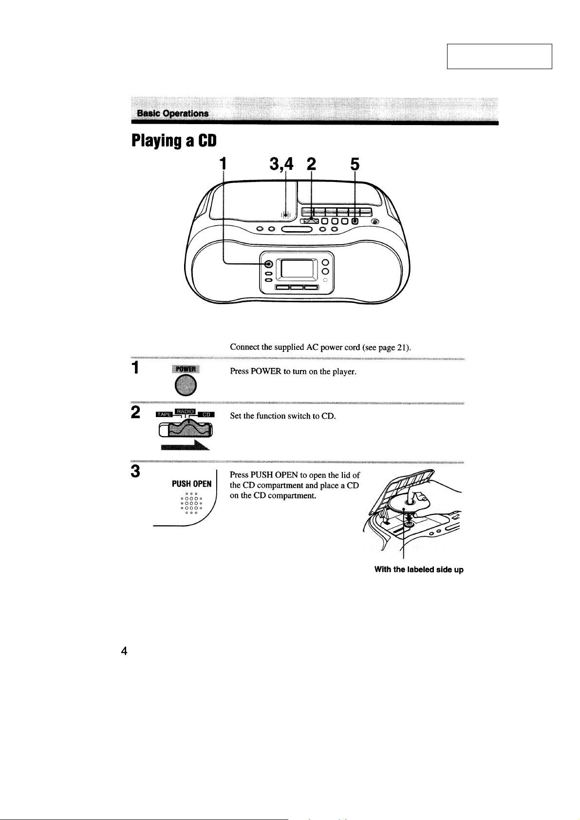
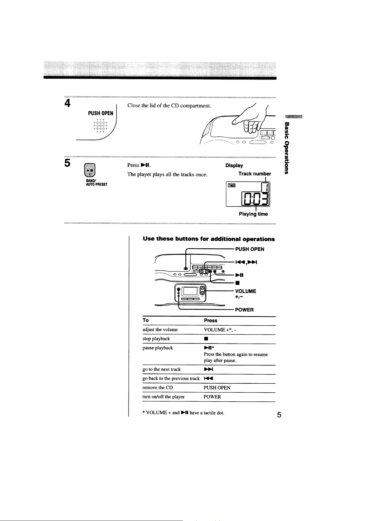
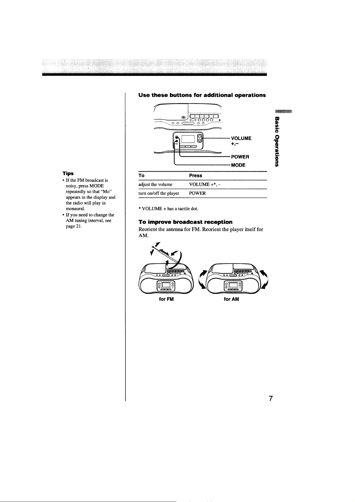
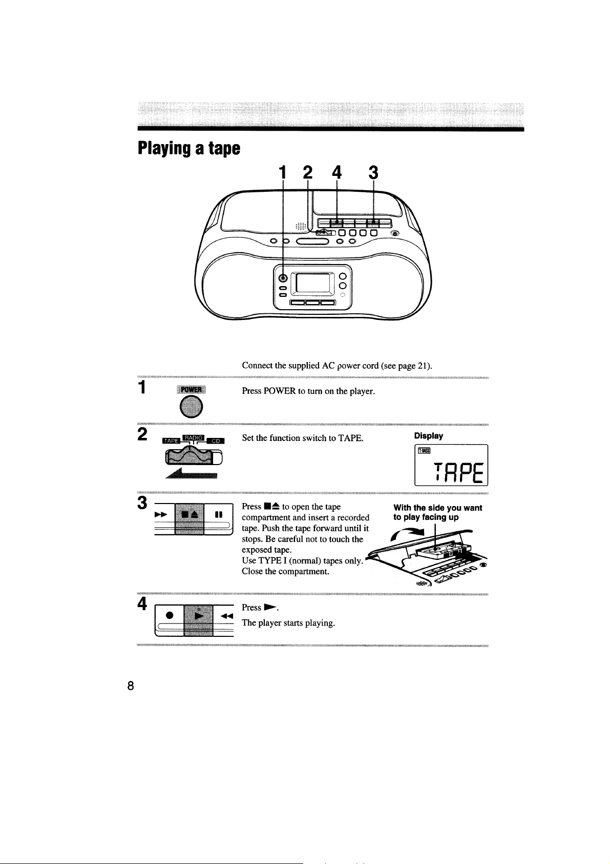
SECTION 2
GENERAL
CSD-A500
This section is extracted
from instruction manual.
5
Page 6
CSD-A500
6
Page 7

CSD-A500
7
Page 8
CSD-A500
8
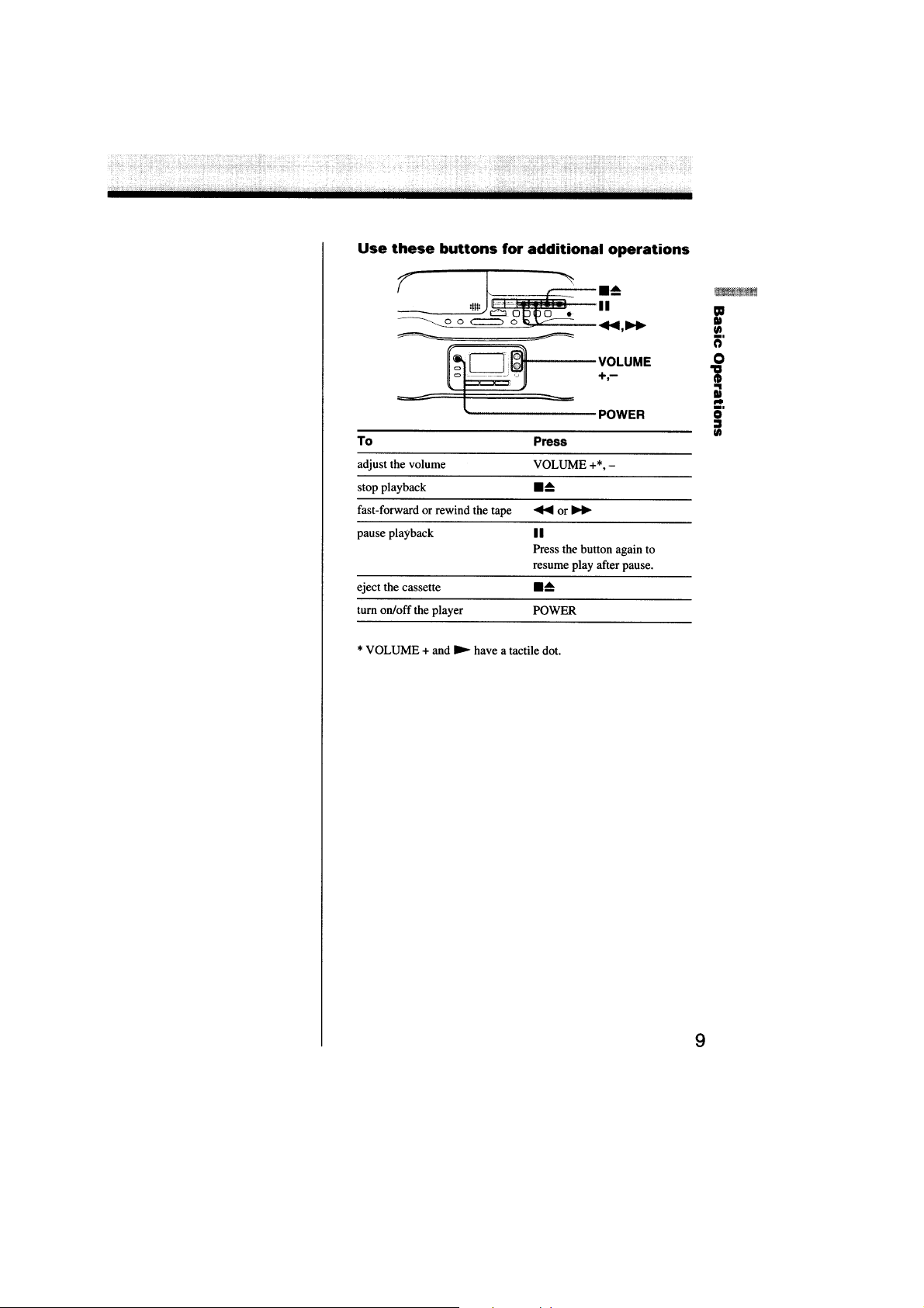
Page 9
CSD-A500
9
Page 10
CSD-A500
10
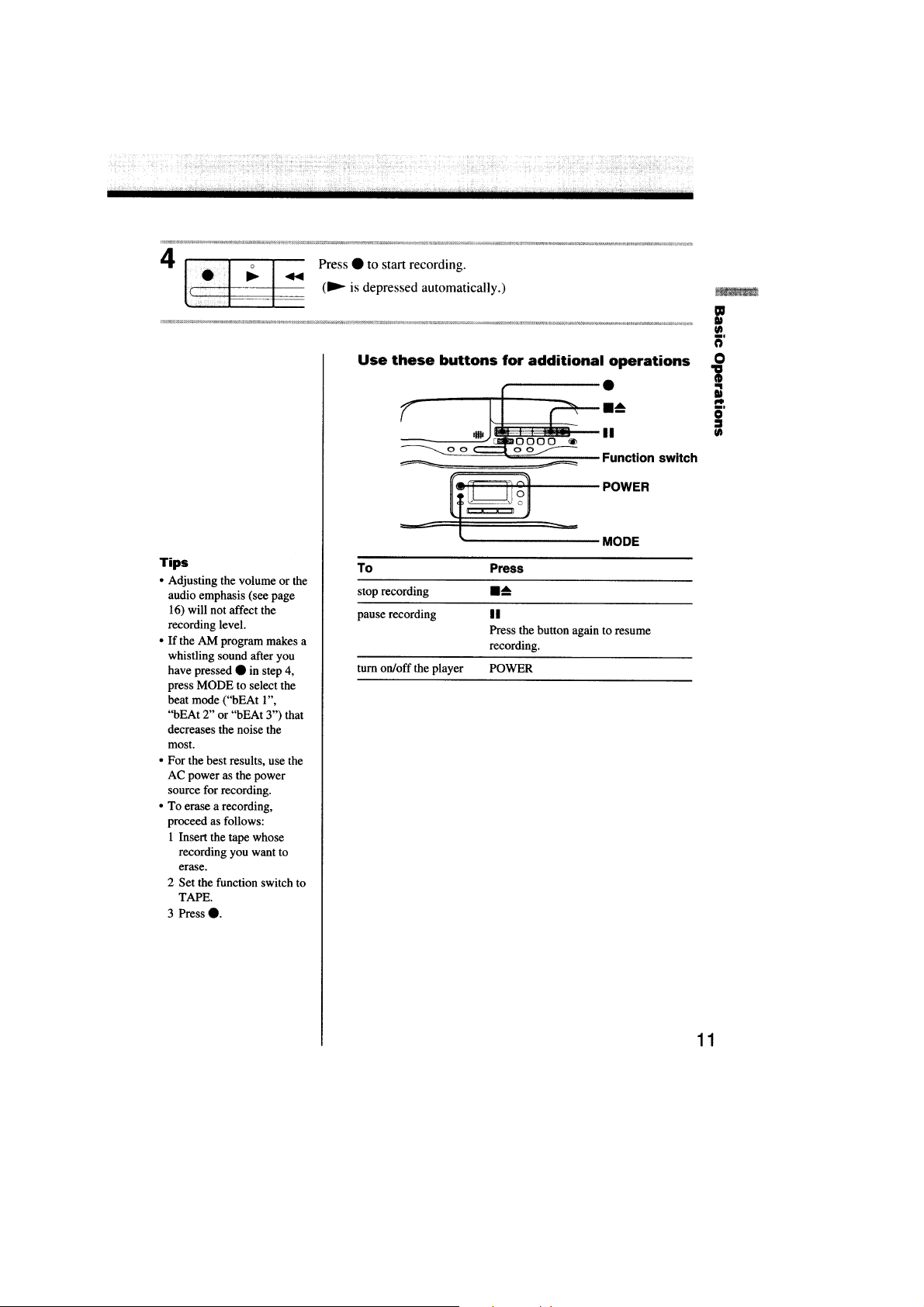
Page 11

CSD-A500
11
Page 12
CSD-A500
12
Page 13
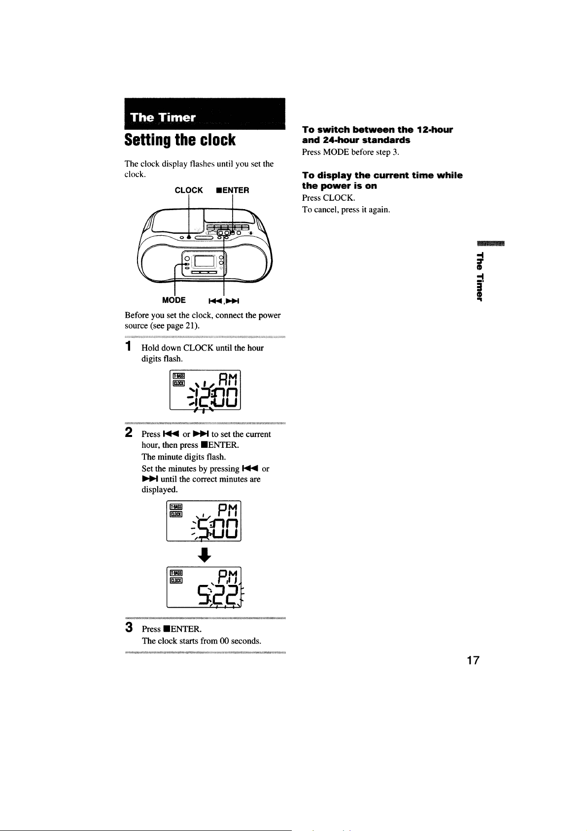
CSD-A500
13
Page 14

CSD-A500
SECTION 3
DISASSEMBLY
• The equipment can be removed using the following procedure.
SET
3-1. CABINET (BOTTOM) ASSY
(Page 15)
3-2. CABINET (TOP) ASSY,
CABINET (FRONT) ASSY
(Page 15)
3-3. LCD BOARD,
LIGHT BOARD
(Page 16)
3-4. BUTTON (PRESET)
(Page 16)
3-9. MD BLOCK ASSY
(Page 19)
3-11. TC BOARD
(Page 20)
3-5. TRANSFORMER BOARD
(Page 17)
3-7. MAIN BOARD, H/P BOARD
(Page 18)
3-8. KEY BOARD
(Page 18)
3-12. HRP301, HE301,
PINCH ROLLER ARM ASSY
(Page 20)
3-6. TUNER BOARD
(Page 17)
3-13. M801, BELT
(Page 21)
3-10. CASSETTE LID
3-14. CD BLOCK ASSY
(Page 21)
3-16. CD BOARD
(Page 22)
3-17. OPTICAL PICK-UP
(Page 23)
(Page 19)
3-15. CD LID
(Page 22)
14
Page 15
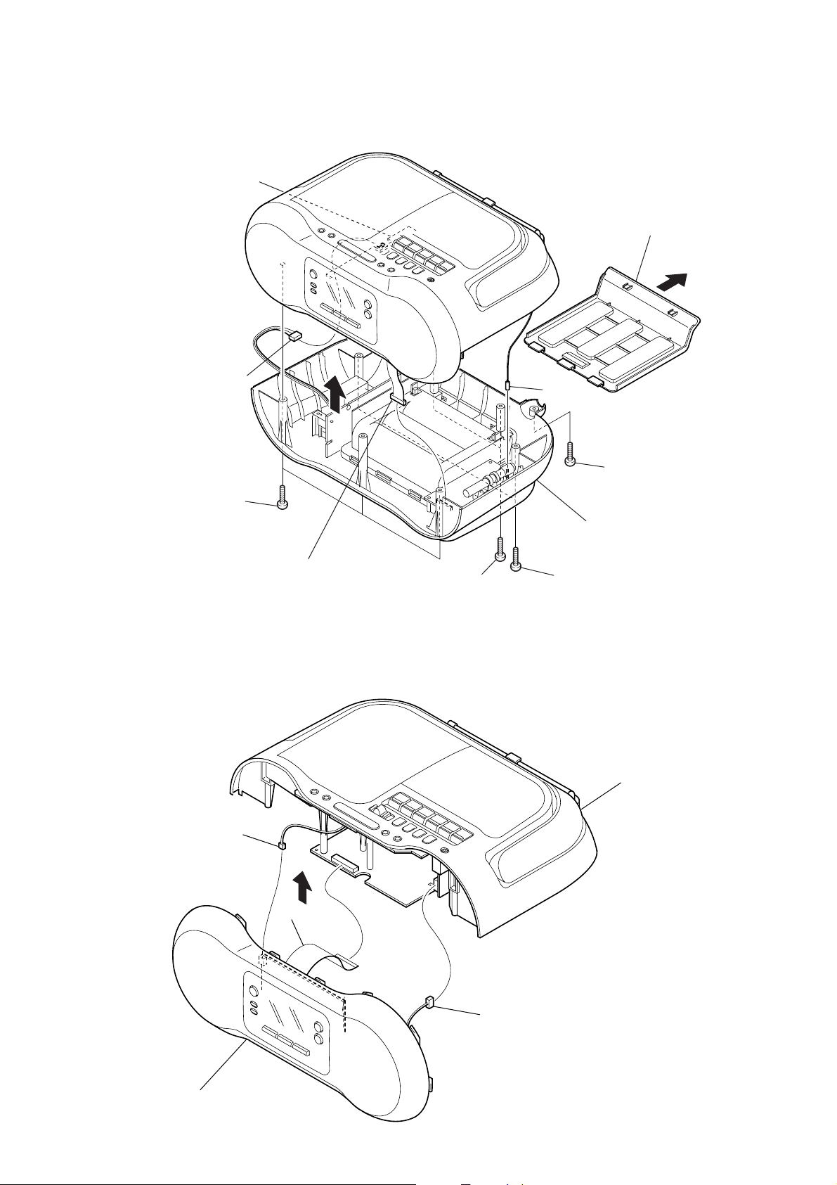
Note : Follow the disassembly procedure in the numerical order given.
d
y
3-1. CABINET (BOTTOM) ASSY
MAIN board
8
CNP901
6
9
CNP2
1
battery case li
CSD-A500
5
three
(2.6)
screws
7
CNP1
4
(2.6)
3-2. CABINET (TOP) ASSY, CABINET (FRONT) ASSY
3
CNP403
1
two
screws
3
(2.6)
screw
2
(2.6)
0
cabinet (bottom) assy
two
screws
6
cabinet (top) ass
5
cabinet (front) assy
4
CNP804
2
CNP203
15
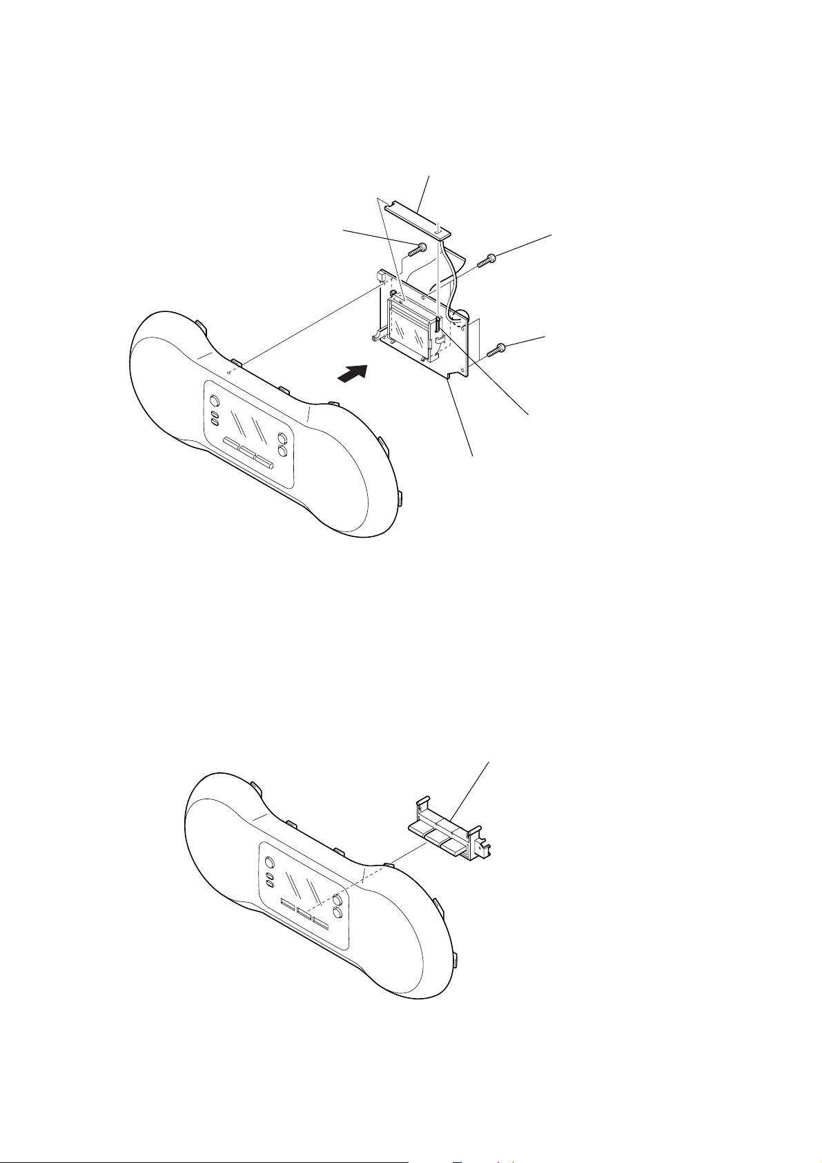
Page 16
CSD-A500
)
)
3-3. LCD BOARD, LIGHT BOARD
2
two
screws
BVTP 2.6 x 10
(+
5
LIGHT board
)
4
claw
3
two
BVTP 2.6 x 10
(+
1
two
screws
BVTP 2.6 x 10
(+
screws
)
3-4. BUTTON (PRESET)
6
LCD board
1
button (PRESET
16
Page 17
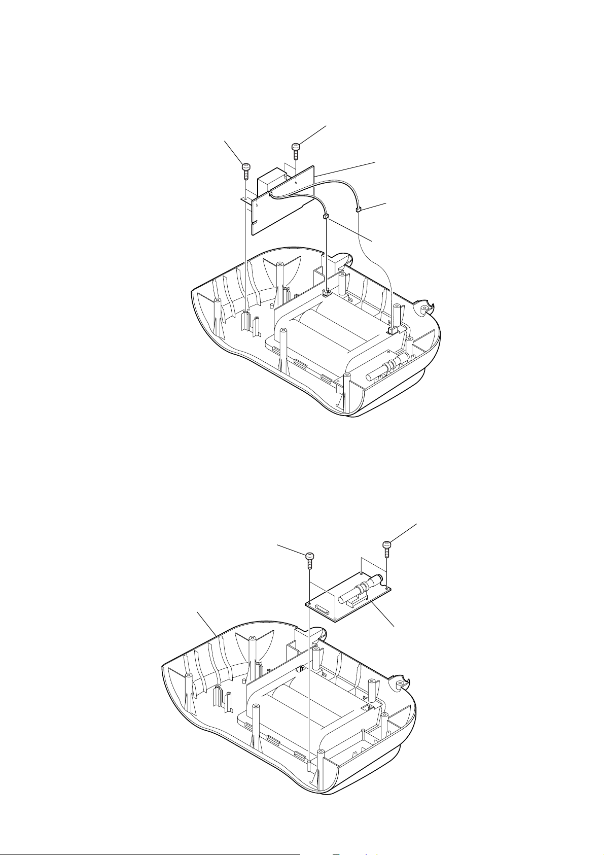
3-5. TRANSFORMER BOARD
d
)
4
two
BVTP 2.6 x 10
(+
screws
CSD-A500
3
two
screws
BVTP 2.6 x 10
)
(+
)
5
TRANSFORMER boar
2
CNP103
1
CNP102
3-6. TUNER BOARD
1
(+
cabinet (bottom)
two
screws
BVTP 2.6 x 10
2
two
screws
BVTP 2.6 x 10
(+
)
3
TUNER board
17
Page 18
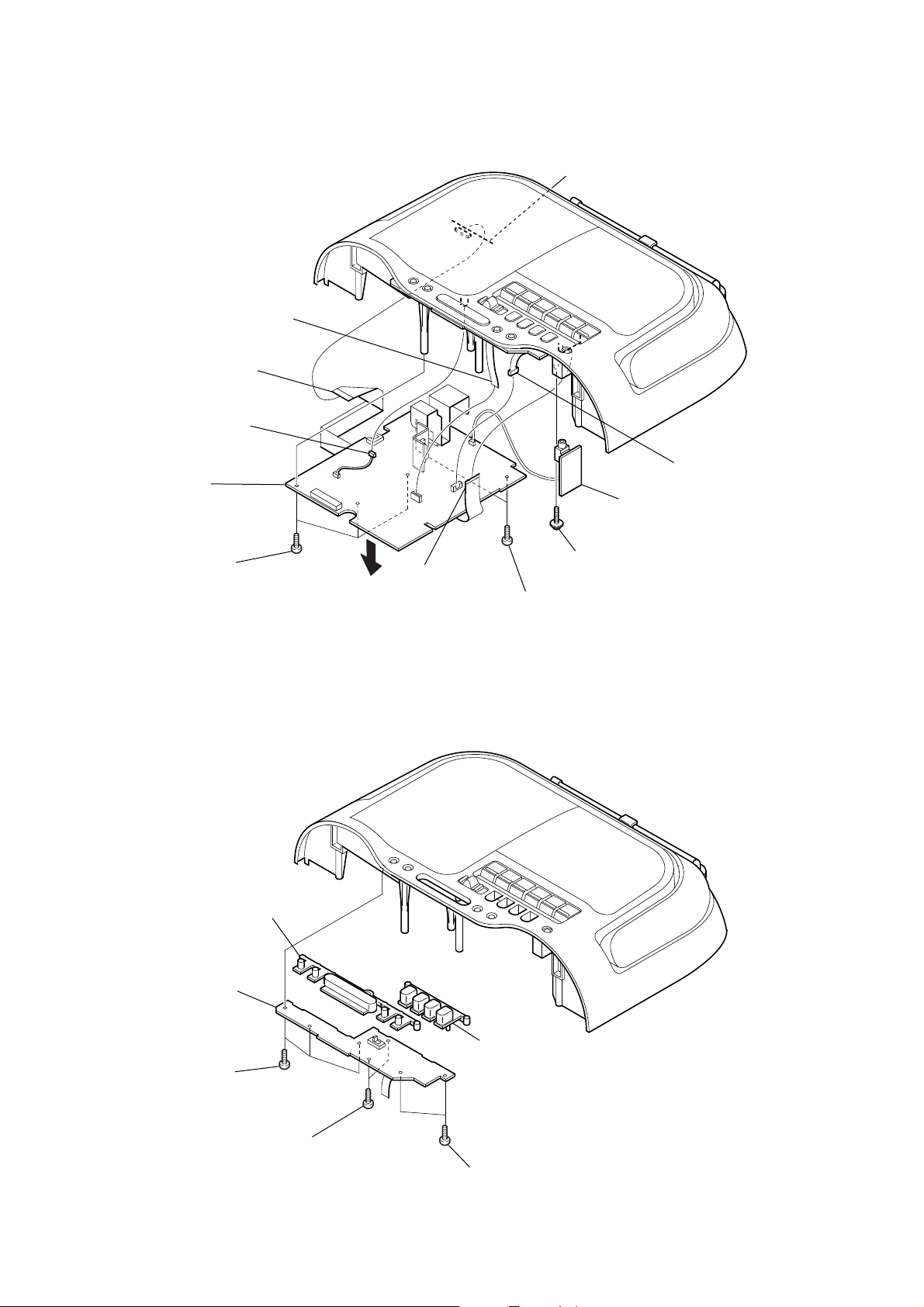
CSD-A500
3-7. MAIN BOARD, H/P BOARD
9
CNP805
3
CNP702
4
connector
qa
MAIN board
CD board
2
H/P board
CNP803
0
5
three
(+
BVTP 2.6 x 10
3-8. KEY BOARD
screws
4
KEY board
)
button (snooze)
7
8
CN303
6
two
screws
(+
BVTP 2.6 x 10
1
screw
(+
PWH 2.6 x 10
)
)
18
3
three
(+
BVTP 2.6 x 10
screws
)
2
two
screws
BVTP 2.6 x 10
(+
button (CD)
)
1
two
screws
(+
BVTP 2.6 x 10
)
Page 19
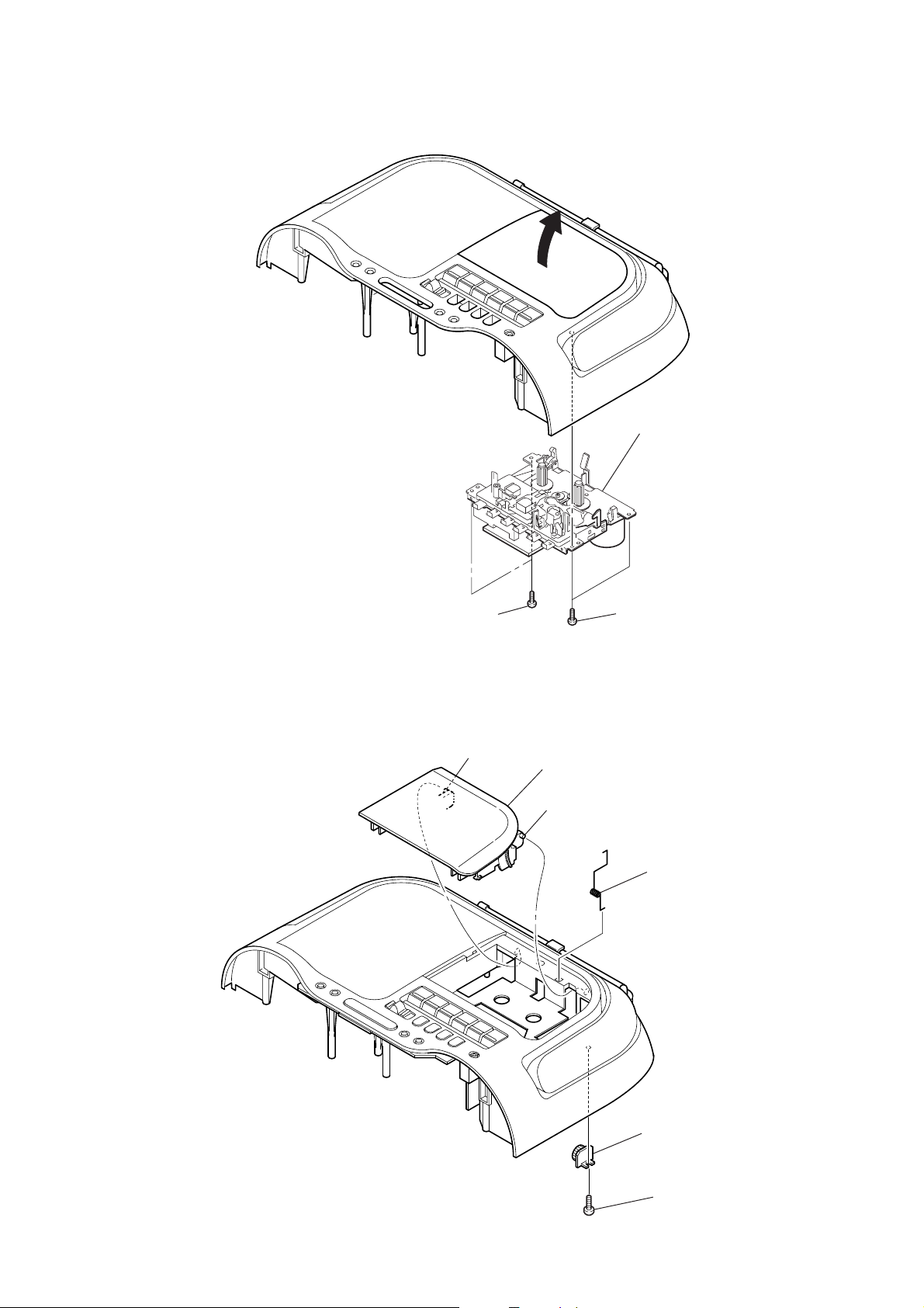
3-9. MD BLOCK ASSY
1
4
MD block assy
CSD-A500
3-10. CASSETTE LID
3
two
screws
BVTP 2.6 x 10
(+
boss
2
two
)
3
cassette lid
boss
screws
BVTP 2.6 x 10
(+
4
)
spring (cassette)
2
1
(+
damper
screw
BVTP 2.6 x 10
)
19
Page 20

CSD-A500
y
3-11. TC BOARD
5
TC chassis
4
(+
screw
BVTT 2 x 4
)
2
Remove the four soldes.
3
TC board
lug
1
screw
BVTT 2 x 4
(+
3-12. HRP301, HE301, PINCH ROLLER ARM ASSY
5
(azimuth)
7
azimuth spring
screw
3
(+B bind)
screw
)
4
lug plate
6
HRP301 (REC/PB head)
1
pinch roller arm ass
20
2
HE301
(ERASE head)
claw
claw
Page 21
3-13. M801, BEL T
4
main belt
3
RF belt
2
1
screw (MB)
5
two
screws
(motor coller)
motor bracket
6
M801
(sub motor assy)
CSD-A500
3-14. CD BLOCK ASSY
4
cover (CD mechanical) assy
7
8
CD block assy
6
two
screws
(+
PWH (B) 2.6
CD cover
)
claws
5
two
PWH (B) 2.6
(+
1
screw
BVTP 2.6 x 10
(+
screws
)
)
3
two
screws
BVTP 2.6 x 10
(+
2
screw
BVTP 2.6 x 10
)
(+
)
21
Page 22

CSD-A500
)
3-15. CD LID
3
CD lid
boss
boss
4
spring (CD
3-16. CD BOARD
4
CNP701
2
damper
1
screw
(+
BVTP 2.6 x 10
3
Remove the two solderings of motor.
)
22
1
(+
screw
BVTT 2 x 6
5
CD board
2
Remove the two solderings of motor.
)
Page 23

)
3-17. OPTICAL PICK-UP
3
screw
(+
PWB tapping (M2)
5
sled shaft
CSD-A500
6
optical pick-up
claw
1
gear (A)
4
)
2
screw
(+
PWB tapping (M2)
23
Page 24

CSD-A500
SECTION 4
MECHANICAL ADJUSTMENTS
SECTION 5
ELECTRICAL ADJUSTMENTS
PRECAUTION
1. Clean the following parts with a denatured-alcohol-moistened
swab :
record/playback head pinch roller
erase head rubber belts
capstan idlers
2. Demagnetize the record/playback head with a head demagnetizer. (Do not bring the head magnetizer close to the erase head.)
3. Do not use a magnetized screwdriver for the adjustments.
4. The adjustments should be performed with the rated power
supply voltage (9V) unless otherwise noted.
Torque Measurement
Mode Torque meter Meter reading
2.95 – 6.86 mN • m
FWD CQ-102C (30 – 70 g • cm)
(0.42 – 0.97 oz • inch)
FWD
Back Tension
FF CQ-201B (more than 60 g • cm)
REW CQ-201B (more than 60 g • cm)
CQ-102C (1.5 – 5.5 g • cm)
0.15 – 0.53 mN • m
(0.021 – 0.076 oz • inch)
more than 5.88 mN • m
(more than 0.83 oz • inch)
more than 5.88 mN • m
(more than 0.83 oz • inch)
TAPE SECTION 0 dB = 0.775 V
• Standard Output Level
Output terminal HP OUT
load impedance 8 Ω
output signal level 0.25 V (–10 dB)
• Test Tape
Type Signal Used for
WS-48A 3 kHz, 0 dB tape speed adjustment
Tape Speed Adjustment
Procedure:
Mode: playback
test tape
WS-48A
(3 kHz, 0 dB)
set
i
jack (J201)
Adjust so that the value on the digital frequency counter is
3,000 Hz.
digital frequency
counter
Ω
8
Tape Tension Measurement
Mode Tension meter Meter Reading
FWD CQ-403A
more than 100 g
(more than 3.53 oz)
Specification Value:
Digital frequency counter
2,910 to 3,090 Hz
Adjust so that the frequency at the beginning and that at the end of
tape winding are between 2,970 to 3,030 Hz.
Adjustment Location:
24
Tape speed adjustment
control inside motor
shield plate
Page 25

CSD-A500
)
TUNER SECTION 0 dB = 1 µV
• AM Section
Setting:
RADIO BAND•AUTO PRESET button: AM
AM RF signal
generator
30% amplitude
modulation by
400 Hz signal
• FM Section
Setting:
RADIO BAND•AUTO PRESET button: FM
FM RF signal
generator
75 kHz frequency
deviation by 1 kHz signal
output level : as low as possible
• Connecting Level Meter (FM and AM)
set
i
jack (J201)
Put the lead-wire
antenna close to
the set.
0.01
µ
F
level meter
(range: 0.5–5 V ac
8
Ω
TP (FM IN)
AM IF ADJUSTMENT
Adjust for a maximum reading on level meter.
T1
450 kHz
AM FREQUENCY COVERAGE
CHECK
Frequency Display 531 kHz 1,611 kHz
Reading on Digital voltmeter 1.0 ± 0.5 V 5.2 ± 0.6 V
Adjustment Part <confirmation> <confirmation>
AM TRACKING ADJUSTMENT
Adjust for a maximum reading on level meter.
L3-1 CT3
621 kHz 1,404 kHz
FM IF ADJUSTMENT
Adjust for a maximum reading on level meter.
T2
10.7 MHz
set
FM FREQUENCY COVERAGE
ADJUSTMENT
Frequency Display 87.5 MHz 108 MHz
Reading on Digital voltmeter 1.3 ± 0.3 V 3.0 ± 0.2 V
Adjustment Part <confirmation> L2
FM TRACKING ADJUSTMENT
Adjust for a maximum reading on level meter.
L1 CT1
87.5 MHz 108 MHz
Adjustment Location: See page 26.
• Connecting Digital Voltmeter (FM and AM)
digital
voltmeter
100 kΩ
TP (VT)
•Repeat the procedures in each adjustment several times, and the
frequency coverage and tracking adjustments should be finally
done by the trimmer capacitors.
25
Page 26

CSD-A500
IC701
C730
R729
R708
C716
C711
C709
FB701
C736
C734
R709
C705
R704
R702
R711
R710
R703
R705
R701
C703
C731
R706
R723
C708
JC703
C743
C744
C745
C742
C707
C717
C739
C738
TP
(VREF)
TP
(TE)
TP
(FE)
TP
(RF)
C732
TY
FY
TX
FX
JW706
JW707
JW708
JW709
JW724
JW726
C746
C747
TP
(RF)
TP
(VREF)
TP
(TE)
– CD board (conductor side) –
Adjustment Location:
– TUNER board (component side) –
TP (FM IN)
(CONDUCTOR SIDE)
T1
AM
IF
ADJUSTMENT
FM
ADJUSTMENT
T1
T2
IF
T2
L1
L3
CT1
IC1
CT1, L1
FM
TRACKING
ADJUSTMENT
L2
L2
FM
FREQUENCY
COVERAGE
ADJUSTMENT
CT3, L3
AM
TRACKING
ADJUSTMENT
CT3
L4
ADJUSTMENT
TP (VT)
(CONDUCTOR SIDE)
L4
AM
FREQUENCY
COVERAGE
IC2
CD SECTION
CD section adjustments are done automatically in this set.
In case of operation check, confirm that focus bias.
FOCUS BIAS CHECK
1. Connect the oscilloscope between IC701 pin 4 and pin qa (or
TP (RF) and TP (VREF)).
2. Insert the disc (YEDS-18). (Part No. : 3-702-101-01)
3. Press the N X (CD) button.
4. Confirm that the oscilloscope waveform is as shown in the
figure below. (eye pattern)
A good eye pattern means that the diamond shape ( ) in the
center of the waveform can be clearly distinguished.
RF level :
0.85 ± 0.2 Vp-p
• RF signal reference waveform (eye pattern)
VOLT/DIV : 50 mV (10 : 1 probe in use)
TIME/DIV : 500 nS
When observing the eye pattern, set the oscilloscope for AC range
and raise vertical sensitivity.
26
Test Point:
Page 27

SECTION 6
DIAGRAMS
6-1. IC PIN DESCRIPTION
• IC801 TMP87CP21CFG-5HF0 (SYSTEM CONTROLLER) (MAIN BOARD)
Pin No. Pin Name I/O Pin Description
1 GND — Ground
2 CF OUT — System clock output (4.19MHz)
3 CF IN — System clock input (4.19MHz)
4 RESET I CPU reset input
5 XT OUT — Sub clock output (32.768kHz)
6 XT IN — Sub clock input (32.768kHz)
7 TEST — Connecting to ground
8 I-CD DOOR I CD door OPEN/CLOSE detection signal input
9 I-REMOCON I Remocon signal input
10 O-SHIFT CLK O Clock shift output
11 O-PLL CLK O Tuner PLL clock output
12 I-PLL DATA I Tuner PLL data input
13 O-PLL DATA O Tuner PLL data output
14 O-CD CLK O CD data clock output
15 I-CD DOUT I CD data input
16 O-CD DIN O CD data output
17 O-PCONT O Power supply control output
18 I-BACK UP I Back-up mode detection signal input
19 I-WP I Wake-up detection signal input
20 O-BUZZER O Buzzer drive signal output
21 O-CD CE O CD chip enable signal output
22 O-CD RST O CD reset signal output
23 O-VOL CLK O Electronic volume control clock output
24 O-VOL DATA O Electronic volume control data output
25 O-LINE IN O LINE IN mode control signal output
26 I-CD WRQ I CD write request input
27 I-CD FSEQ I CD frame synchronized signal detection input
28 I-CD DRF I CD focus OK detection signal input
29 O-MAIN MUTE O Main mute control signal output
30 I-KEY0 I Key A/D input
31 I-KEY1 I Key A/D input
32 I-KEY2 I Key A/D input
33 I-KEY3 I Key A/D input
34 I-V MONITOR I Not used. (Open)
35 BATT-CHK-H I Battery reverse voltage check input (9V)
36 BATT-CHK-M1 I Battery reverse voltage check input (6V)
37 BATT-CHK-M2 I Battery reverse voltage check input (3V)
38 VASS — Ground
39 VAREF — A/D reference voltage input (+3.3V)
40 VDD — Power supply (+3.3V)
41 O-T BASS O T-BASS control signal output
42 O-BEAT1 O AM beat select signal output
43 O-BEAT2 O AM beat select signal output
44 O-LIGHT O LCD backlight control signal output
45 O-PLL MUTE O Tuner PLL mute signal output
46 O-PLL CE O Tuner PLL chip enable output
47 O-CD O CD power control signal output
48 O-TP O TAPE power control signal output
49 O-TU O Tuner power control signal output
50 I-SUFFIX1 I Designation setting input
CSD-A500
27
Page 28

CSD-A500
Pin No. Pin Name I/O Pin Description
51 I-SUFFIX2 I Designation setting input
52 I-DECK I Deck mode detection signal input
53 I-AC/DC I AC/DC mode detection signal input
54 I-SYNC REC I CD to TAPE synchro-recording start signal input
55 I-SUFFIX3 I Designation setting input
56 CLOCK DET I Clock 12-hour/24-hour select initial setting
57 SEG15 O LCD segment data output
58 SEG14 O LCD segment data output
59 SEG13 O LCD segment data output
60 SEG12 O LCD segment data output
61 SEG11 O LCD segment data output
62 SEG10 O LCD segment data output
63 SEG9 O LCD segment data output
64 SEG8 O LCD segment data output
65 SEG7 O LCD segment data output
66 SEG6 O LCD segment data output
67 SEG5 O LCD segment data output
68 SEG4 O LCD segment data output
69 SEG3 O LCD segment data output
70 SEG2 O LCD segment data output
71 SEG1 O LCD segment data output
72 SEG0 O LCD segment data output
73 COM3 O LCD common data output
74 COM2 O LCD common data output
75 COM1 O LCD common data output
76 COM0 O LCD common data output
77 VLCD — LCD voltage input
78 (NCO) — Not used. (Open)
79 (NCO) — Not used. (Open)
80 (NCO) — Not used. (Open)
28
Page 29

6-2. BLOCK DIAGRAM — CD SECTION —
A
C
B
D
E
F
LD
PD
VREF
OPTICAL PICK-UP
BLOCK
(KSS-213R)
TRACKING
COIL
FOCUS
COIL
M702
SLED
MOTOR
M701
SPINDLE
MOTOR
(LIMIT)
M
M
S701
A
C
B
D
E
F
LD
PD
VR
VREF
T+
T–
F+
F–
Signal path
: CD
LD POWER
CONTROLLER
SL+
SL–
SP+
SP–
Q701
VREF
7
9
10
80
79
11
12
11
17
18
26
27
2
1
FIN2
FIN1
TIN1
TIN2
LDD
APC
LDS
VREF
T+
TRACKING
T–
F+
F–
SL+
MOTOR
SL–
SP+
SPINDLE
MOTOR
SP–
SLED/SPINDLE
MOTOR DRIVER,
TRACKING/FOCUS
COIL DRIVER
IC702
COIL
DRIVE
FOCUS
COIL
DRIVE
SLED
DRIVE
DRIVE
PH/BH
MUTE
VREF
OPIN
TIN
FIN
SLIN
SPIN
CSD-A500
LCHO
RCHO
D901 – 904
42
45
SOFT START
RELEASE
CONT4
INTERPOLATION
ATTENUATION
DEEMPHASIS
RES
RST
CD
VDD
(SW)
MUTE
&
SYSTEM SERVO PROCESSOR,
DIGITAL SIGNAL PROCESSOR
PLL
VCEC
COMMAND
INTERFACE
DICECL
CE
DIN
BATTERY
CHECK
M6V
L3V
BATTERY
CHECK
Q805,808,809
WP
SLICE
LEVEL
CONTROL
A/D
CONVERTER,
SERVO
PROCESSOR
CLV,CAV
CONTROL
SWITCH
SYSTEM CONTROLLER
IC801 (1/2)
CD DOOR
8
S801
PUSH
OPEN
TU17P-CONT
49 37 36 35
RF
48
CONVERTER
TDDTD
20
TD
9
FD
19
7
SL
25
SP
3
23
VREF
15
D/A
FDD
SPDO
21 22 23
FD
SP
EFMIN
3
AGC
HFL
PH(RFENV)
FE
TE
VREF
SLDO
SL
4
ERROR
CORRECTION
AUDIO CD
FRAME SYNC
DETECT,PROTECT
INSERT
EFM DECODER
GENERAL
PURPOSE
PORT
CONT1
FSEQ
DRF
67
31 72 25 66 63 61 62 49 4865 64
28 27 16 21 14 26 1522
DRF
FSEQ
Q812
D804
RF AMP,
IC701
WRQ
CLK
WRQ
H9V
8FS
DIGITAL
FILTER
&
1-bit DAC
GENERATOR
DO
16.93MHz
DOUT
AC/DC
53
POWER
CONTROLLER
Q902,903
CLOCK
XIN
X701
Q802
LPF
XOUT
AC/DC
(Page 30)
D910
POWER
CONTROL
Q813,814
6V
+6V
REG
Q904
CD 3.3V
RADIO 6V
3.3V
REG
Q905-907
Q901
TRANSFORMER
SOFT START
3V
3V
3V
CD_IN_ L
1
CD_IN_R
T901
POWER
DRY BATTERY
SIZE " D "
(IEC DESIGNATION R20)
6PCS,9V
(Page 30)
(Page 30)
3
J901
AC IN
(Page 30)
CD
2
VOL 6V
+6V
REG
Q908
3.3V
(SW)
POWER
SWITCH
Q811
3.3V
+3.3V REG
IC901
VCC 9V
23
29 29
Page 30

CSD-A500
6-3. BLOCK DIAGRAM — MAIN SECTION —
HRP301
RECORD/PLAYBACK
HEAD
L-CH
R-CH
HE301
ERASE HEAD
ANT1
FM/TV
TELESCOPIC
ANTENNA
(Page 29)
S301
(REC/PB)
REC
R.RO
9
R.IN
8
R.LINE
SEG0
1 2 3 4
PD
16
LP-IN
17
LP-OUT
18
AM
OSC
AM
MIX
OSC
D1 D2
14
4
24
5
6
T301
PLL
CE
DATA
1346 11 12
DI
CE
11 12
FM
MIX
FM
2124
L.RO
L.LINE
L.IN
REF
CLK
CL
AM IN
1920
FM OSC
CD_IN_R
1
CD_IN_L
-1 -2
PB
6V
VDD (SW)
D914
CT3
CT3,L3
TRACKING
54
REC
D3
L3
AM
FERRITE-ROD
ANTENNA
RADIO 6V
AM
CT1,L1
FM
TRACKING
Q302
FREQUENCY
COVERAGE
Q303
AM
42
IBEAT1
L4
43
BEAT2
|
COM3|COM0
SEG15
57–7273 – 76
LIQUID CRYSTAL
DISPLAY PANEL
LCD401
L4
RADIO 6V
AM OSC
AM
RF-IN
22 4 6
FM
RF-IN
2
FM
RF-OUT
DET
ALC 2
RADIO L
REC
21 22 16
REC BIAS OSC
Q301
SYSTEM CONTROLLER
DATA
XTIN5XTOUT
6
32.768kHz
DO
FM IN
OSC-OUT
MIX-OUT
L2L1 CT1
RADIO 6VRADIO 6V
3
X802
XOUT
20 19
FM/AM FRONT END, IF AMP,
T1
T1
AM IF
L2
FM
FREQUENCY
COVERAGE
REC/PB
PRE AMP
IC301
L.RAD
R.RAD
TU_IN_R
TU_IN_L
IC801 (2/2)
CFIN2CFOUT
X801
4.19MHz
FM/AM PLL
IC2
XIN
X1
75kHz
FM MPX
IC1
CF4
RADIO 6V
CF2
RADIO 6V
L.LO
20
R-CH
18
17
15
D801
TAPE
48
TP
CD
RESET
4
1
RESET
IC802
2
3.3V
MO/ST
13
14 17 13 18
LPF2/MO-ST
10
IF
BUFFER
IF IN
IF-OUT
TAPE
SHIFT CLK
10
CLOCK
CONTROL
Q803,804
AM
IF-IN
FM
IF-IN
7
R.LO
LINE
LINE AMP
PLL MUTE
45
Q1031
IF CUT
DET
DET
RADIO 6V
Q205
CD
(Page 29)
BACK-UP DET
AM
FM
QUAD
10
2
18
1
IC803
2
VCC 9V
BUFFER
T2
8 7
BACK-UP
BAND8ST-IND
7
ST-IND
LPF1/BAND
DET-OUT
AF
T2
FM IF
IC201
ELECTRONIC VOLUME
VIN2
VOL AMP
LOGIC
CLOCK4DATA
5
2347 24
CLK
VOL
6V
16 15
VOUT2
DATA
LIGHT
44
LCD BACK LIGHT
ON/OFF CONTROL
Q841,842
MPX-IN
FM
MPX
25
IF CUT
LINE IN
(Page 29)
MUTE
T-BASS
CONTROL
Q207
41
T.BASS
19
WP
4
LED402-413
(LCD BACK LIGHT)
R-OUT
11
L-OUT
12
20
BUZZ
WP
Q810,D805,806
TU_IN_R
R-CH
MUTE
Q209
29
52
DECK
MAIN MUTE
POWER AMP
IC202
6
121
VCC(9V)
LEVEL
DETECT
D202
TAPE PLAY
DETECT
Q801
KEY030KEY131KEY232KEY3
33
R-CH
2
SOFT START
3
VDD (SW)
(Page 29)
REMOTE
REMOCON
VDD (SW)
KEY3
KEY2
KEY1
KEY0
9 1
AC/DC
LED401
OPR/BATT
S414-418
S407-409,411-413
S402-406,410
S401
CONTROL
RECEIVER
IC402
D1051
KEY NETWORK
3
Signal path
: FM
: MW
: TAPE PLAY
: TAPE REC
: CD
R-ch is omitted due to same as
L-ch.
SP201
SPEAKER
(L-CH)
SP101
SPEAKER
(R-CH)
S301
(TAPE POWER)
M
M801
CAPSTAN/REEL
MOTOR
J201
PHONES
3030
Page 31

CSD-A500
6-4. CIRCUIT BOARDS LOCA TION
CD board
KEY board
LIGHT board
LCD board
TRANSFORMER board
H/P board
BATT 2 board
MAIN board
TC board
TUNER board
BATT 1 board
• Waveforms (Mode: PLA Y)
— CD Board —
500mV/div 0.5µsec/div
1
0.85±0.2Vp-p
IC7014 (RF)
100mV/div 20µsec/div
2
1.8V
Approx. 100mVp-p
IC701qd (FE)
100mV/div 20µsec/div
3
1.8V
Approx. 100mVp-p
IC701qg (TE)
1V/div 0.05µsec/div
4
3.2Vp-p
16.93MHz
IC701rk (XOUT)
• Waveforms
— MAIN Board —
2V/div 10µsec/div
1
4.19MHz
IC801 2 (CFOUT)
2V/div 10µsec/div
2
32.768kHz
IC801 5 (XTOUT)
• Waveforms
— TC Board —
0.1V/div 5µsec/div
1
19.5µsec
Q301 C (REC)
10V/div 5µsec/div
2
1.4Vp-p
2.6Vp-p
4Vp-p
• Waveforms
— TUNER Board —
0.5V/div 5µsec/div
1
75kHz
IC2 w; (XOUT)
40Vp-p
19.5µsec
T301, HRP301 (YEL)
1.5Vp-p
31 31
Page 32

CSD-A500
THIS NOTE IS COMMON FOR PRINTED WIRING
BOARDS AND SCHEMATIC DIAGRAMS.
(In addition to this, the necessary note is
printed in each block.)
Common Note on Schematic Diagrams:
• All capacitors are in µF unless otherwise noted. pF: µµF
50 WV or less are not indicated except for electrolytics
and tantalums.
• All resistors are in Ω and 1/
specified.
f
•
: internal component.
• C : panel designation.
Note: The components identified by mark 0 or dotted line
with mark 0 are critical for safety .
Replace only with part number specified.
• A : B+ Line.
• H : adjustment for repair.
•Total current is measured with no cassette installed.
• Power voltage is dc 9V and fed with regulated dc power
supply from battery terminal.
•Voltages are taken with a VOM (Input impedance 10 MΩ).
Voltage variations may be noted due to normal production tolerances.
•Waveforms are taken with a oscilloscope.
Voltage variations may be noted due to normal production tolerances.
• Circled numbers refer to waveforms.
• Signal path.
F : FM
f : AM
E : PB
a : REC
J : CD
Common Note on Printed Wiring Boards:
• X : parts extracted from the component side.
• Y : parts extracted from the conductor side.
f
•
: internal component.
• : Pattern from the side which enables seeing.
4
W or less unless otherwise
• Refer to page 31 for Circuit Boards Location.
6-5. PRINTED WIRING BOARD — CD SECTION — • Refer to page 32 for Common Note on Printed Wiring Boards.
1
234567
A
JC702
JC701
B
C
D
E
F
G
OPTICAL
PICK-UP
BLOCK
(KSS-213R)
C733
C750
C706
C732
C738
C739
M701
SPINDLE
MOTOR
JW716
JW715
CNP701
115
R712
JW714
JW713
JW711
JW710
R706
(VREF)
JW709
R701
TP
R709
R705
R703
TP
(TE)
C707
JW706
R702
JW708
R710
R704
C736
JC703
TX
FX
JW705
M
10216
JW712
C704
R711
R708
C705
TP
(RF)
TP
C734
(FE)
C742
C708
JW707
TY
FY
C727
C731
R723
C751
C743
S701
(LIMIT)
Q701
C701
JW725
C703
IC701
C709
JW703
R741
JW722
R727
R730
R729
JW726
R728
C711
JW717
C702
JW723
C746
C744
C716
JW702
R707
C730
JW701
JW718
JW721
C728
C729
R726
JW724
C747
C745
C717
FB701
C740
R732
R714
R715
IC702
C741
R725
R731
C721
C735
R724
C726
R722
X701
M702
SLED
MOTOR
C723
R721
C725
R719
R720
R717
R718
JW727
R716
C720
JC704
1-688-377- (11)
JW728
C722
JW719
JW720
C724
TP
(L-CH)
R744
M
JW729
L706
11
C755
C754
TP
(R-CH)
R743
(Page 38)
CNP702
3232
Page 33

• Refer to page 31 for Waveforms.
• Refer to page 32 for Common Note on Schematic Diagrams.
6-6. SCHEMATIC DIAGRAM — CD SECTION — • Refer to page 45 for IC Block Diagrams.
C738
C739
C732
R724
R709 R710
C703
C704
C743
C707
S701
CNP701
R712
R701
R702
R703
R704
R705
R706
C750
L706
C751
R707
C733
C702
Q701
C701
C706
C708
C742
C731
R711
C734
C736
R708
C705
JC703
C744
C747
R730
R729
R727R728
C730
C727
C726
C724
C725
C721 R717
C720
C722
C723
C746
C745
R720
R719
R722
C728
C729
R725
R731
R726
IC701
R716
R718
R721
IC B/D
C717
FB701
C716
R732
R715
R714
CSD-A500
(Page 37)
C755
C754
CNP702
X701
JC704
TP
TP
M702
M701
JC702
JC701
R743
R744
•Voltage and waveforms are dc with respect to ground
under no-signal (detuned) conditions.
no mark : CD PLAY
Note: The components identified by mark 0 or dotted line
with mark 0 are critical for safety.
Replace only with part number specified.
IC702
C741
R741
C740
IC B/D
C709
C711
C735
R723
33 33
Page 34

CSD-A500
• Refer to page 31 for Circuit Boards Location.
6-7. PRINTED WIRING BOARD — TUNER SECTION — • Refer to page 32 for Common Note on Printed Wiring Boards.
A
B
C
D
E
F
G
1
CNJ802
(Page 38)
CNJ801
(Page 38)
234567891011 12 13 14
L3 AM FERRITE-ROD ANTENNA
WHT
BLK
BLK
BLK
BLK
BLK
WHT
BLK
BLK
BLK
BLK
C26
C27
TP
(VT)
CNP1
JC1
R61
R60
R59
R58
JC33
C65
L21
JC34
R63
R10
JW3
R65
C62
C63
R13
R94
C61
C60
C29
C51
C66
C52
C68
IC2
X1
JC2
R56
C55
R52
C59
C57
R4
R50
C53
R53
C95
C37
R54
JW5
JW4
R51
C54
R91
JC11
C47
JW6
C39
JC4
JW7
JC5
R40
C41
L3
C49
C42
CT3
C21
R11
C43
JC3
L4
JC12
R30
JW9
C30
C56
C22
D3
D2
C31
JW10
R41
C24
C23
R31
R24
C20
C33
L11
L2
R92
C77
JC24
JW8
R32
C78
C80
C32
CT1
C14
C15
IC1
C11
R2
D1
C34
C35
C12
C7
D11
D10
C4
L1
TP
FM
IN
C1
C18
C9
JW12
JW11
T2
R3
CF2
JW13
CF4
C8
C10
JC13
T1
CNP2
JW2
R1
JC6
11
1-688-455- (11)
ANT1
FM/TV
TELESCOPIC
ANTENNA
• Semiconductor
Location
Ref. No. Location
D1 C-10
D2 D-8
D3 D-8
D10 B-12
D11 B-12
IC1 E-10
IC2 E-5
3434
Page 35

• Refer to page 31 for Waveforms.
• Refer to page 32 for Common Note on Schematic Diagrams.
6-8. SCHEMATIC DIAGRAM — TUNER SECTION — • Refer to page 46 for IC Block Diagrams.
CSD-A500
ANT1
CNP2
JC24
L3
D3
C34
CT3
R41 C49
CT1
C35 C33
L1
D1
JC12 JC11
0
C41
C42
C43
R40
C47
R30R32 C80
C31
D2
22p
L2
C30
R31
JC3
C39
C37
C24
L4
R11
C21 C22
R50
R91
C51 C52
X1
R52 R65
C53
R51
C59
R53
C54
R54
C95
C55
C65
R63
TP
C56
C57
IC B/D
R24 C20
C23
IC2
IC B/D
JC4
C61
C62
C63
R60R61 R59 R58
R92
C66
IC1
JC6
CF4
C12
C7
C9
T2
JC13
C11
TP
C1
R2
T1
C68
C60
R94
R13
JC5
R4
R56
L21
CNP1
(Page 37)
R3
C32 C4 C8
D11D10
C10
•Voltage and waveforms are dc with respect to ground
under no-signal (detuned) conditions.
no mark : FM
(): AM
R1
CF2
C18
C14 C15 C77 C78
JC33
JC2
JC34
C29
R10
C27
JC1
C26
(Page 37)
35 35
Page 36

CSD-A500
• Refer to page 32 for Common Note on Schematic Diagrams.
6-9. SCHEMATIC DIAGRAM — MAIN SECTION (1/2) — • Refer to page 47 for IC Block Diagrams.
IC B/D
C275
R252
C277
C276
C235
R286
R289
R251
C236
R243
C231
R245
R246
C232
R244
R249
R253
R254
R250
R255
C233
C234
R256
C271
Q205
Q206
C273
C272
C274
IC201
R285
Q908
IC B/D
C294
C293
R267
R257
C237
R287
R288
C238
R258
R268
C296C295
C257
C258
R295
R262
R261
Q207
Q208
R263
R264
C261
C262
R269
R270
C243
C242
C244
C241
R293
R238
C281
R275
R276
R283
R284
Q210
R901
Q209
R280
R279
Q901
R241
R242
C910
R259 C247
C245
C249
R271
R272
C250
C246
R260
R1010
R281
IC202
R282
C248
C265
C289
C251
C252
D202
R248
C266
C298
R247
C290
R290
C288
R292
R291
C255
C256
C292
C291
CNJ201
CNJ202
R297
R296
R299
R298
CNP203 CNJ204
SP201
SP202
J201
PHONES
(Page 37)
IC901
D914
C928
R924R925
C923
C927
C922
C920
R923
R927
R926
•Voltage and waveforms are dc with respect to ground
under no-signal (detuned) conditions.
no mark : FM
<>: CD PLAY
R921
CNP901
Q904
Q907
R913
R914
C916
R912
907
D
C917
909
D
C915
Q905
906
Q
R922
C914
C912
R910 R911
C913
906
D
Q903
R907 R908 R909
R906
Q902
R917
R905
(Page 44)
C911
R918
3636
Page 37

• Refer to page 31 for Waveforms.
6-10. SCHEMATIC DIAGRAM — MAIN SECTION (2/2) — • Refer to page 32 for Common Note on Schematic Diagrams.
CNP804
CSD-A500
S801
PUSH OPEN
(Page 42)
(Page
33)
(Page 42)
CNJ808
CNP805
C818
C819
D805
R951
R953
R952
D806
R959
R960
R957
R898
C820
R1067
Q810
IC803
C873
C870
R804
D808
Q803
R956
R1068
C869
R803
R805
R824
R823
Q804
C817
C816
C838
IC802
C839
C832
C801
C802
C833
C803
C804
C807
C808
C809
C810
C811
C812
R817
C814
C815
X802
R1022R1021
X801
R802
C805
Q811
R801
R806
R807
R808
R809
R810
R811
R812
R813
R814
R815
R816
R818
R819
R820
R821
R822
C834
R825
R896
R826
R895
R827 R828
R893R894
R892
R832 R834 R836
R891
IC801
TMP87CP21CFG-5HF0
R838
C1043
Q813
Q842
C1044
R1043R1041
R1032
C1045
Q814
CNJ801
CNJ802
(Page 35)
(Page 35)
(Page 40)
R1054
Q841
L803
R883R884R885R886
R1053
D1035
C1051
C827
C828
R872
R871
R870
R868
R866
R864
R862
R860
R859
R858
R1013
R857
R1012
R856
R1011
R855
R854
R853
R851
R849
R847
R882
R881
R880
R879
R878
R877
R876
R875
R1034
L802
L801
C829
C831
C830
C1073
C1072
C1071
R869
R867
Q801
R861
R852
R850
R848
D810
C1074
R1051
R1052
Q802
R888R889R890
R887
D1051
R1031
R1033
D801
R1063
R1061
Q1031
R963
R1064
R1062
R1055
R1066
R1065
R990
R994
D804
R995
Q812
D802
D803
•Voltage and waveforms are dc with respect to ground
under no-signal (detuned) conditions.
no mark : FM
(): PB
[]: REC
<>: CD PLAY
R996
R897
C821
C822
C823
R829
R833
R831
R835
R837
R830
37 37
R839
C824
R841
C825
R844
R845
R846
C826
R842 R843
Q805
Q809
Q808
R968
R967
CNP803
(Page 36)
M801
S802
Page 38

CSD-A500
• Refer to page 31 for Circuit Boards Location.
6-11. PRINTED WIRING BOARDS — MAIN SECTION — • Refer to page 32 for Common Note on Printed Wiring Boards.
• Semiconductor
Location
Ref. No. Location
D202 A-5
D801 G-3
D802 F-5
D803 F-5
D804 F-6
D805 F-7
D806 F-6
D808 G-10
D810 G-5
D906 D-6
D907 E-8
D909 E-8
D914 D-5
D1035 I-7
D1051 I-5
IC201 B-4
IC202 B-8
IC801 H-7
IC802 H-9
IC803 H-9
IC901 D-5
Q205 C-3
Q206 B-3
Q207 B-5
Q208 B-5
Q209 C-7
Q210 B-7
Q801 E-4
Q802 I-6
Q803 H-8
Q804 H-8
Q805 F-5
Q808 F-5
Q809 F-5
Q810 F-7
Q811 G-5
Q812 F-6
Q813 G-3
Q814 G-3
Q841 G-5
Q842 G-4
Q901 C-8
Q902 D-7
Q903 D-7
Q904 D-6
Q905 E-8
Q906 E-8
Q907 E-9
Q908 C-3
Q1031 I-3
A
B
C
D
E
F
G
H
1
M801
S802
(Page 34)
(Page 39)
(Page 41)
(Page 34)
I
2345678910111213
JW853
CNJ801
JW852
R1031
C295
R243
CNJ802
C1045
JW855
Q813
JW847
C232
C231
JR852
R1032
Q1031
C1044
R1033
JW991
JW912
JW964
R244
R246
R245
R255
Q908
C296
C1043
Q814
C233
Q206
R249
R256
Q205
R1043
R1041
R250
R254
C234
R295
JW992
D801
JR808
R253
JW949
JW947
JR801
R251
JW988
Q801
JR809
JW846
JW849
C275
JW1005
C271
JW993
JW827
JW826
JW825
JW803
JW845
JW848
JW850
JR802
C236
C273
C276
R252
C277
JW1003
JW1004
JW823
JW822
IC201
CNP803
R1054
R1055
JW816
C928
JW824
Q842
JW860
C274
C235
R289
JR810
JR807
C272
R924
R925
R286
JW812
JW811
C238
R258
R268
R288
R257
C818
C819
JW818
JW817
R1012
R267
JW987
D914
C927
CNP805
JW854
Q841
JR811
JW815
C237
C922
R285
JW229
C923
JW828
JR812
R1011
R1061
R1062
R1065
R1051
R1052
D202
C258
C262
C261
R287
C257
IC901
R923
JW829
C1074
D810
JW819
JR813
JW814
R856
JW809
JW808
JW801
C265
R261
R926
JW820
R852
R262
R264
Q208
R263
Q207
C920
JW831
JW862
R855
JW802
R927
JW950
JW856
JR804
JR806
D803
D802
R850
JW804
R270
R269
JW945
Q805
L802
R848
JW813
R1063
R1064
R1066
R247
C266
R911
R968
Q809
L803
R853
R861
C831
C830
JW805
D1051
R248
R922
R996
R851
R854
C242
C241
R824
R910
JW943
R967
Q808
R860
R1053
JR821
R842
R859
R867
JW942
R845
C825
C1073
R862
R869
JW994
R921
C914
R994
R990
Q811
R1013
R858
R823
JW1002
JW986
JW913
JW938
Q812
R995
JW821
L801
R847
R841
C828
Q802
CNJ201
JW1001
D906
JW944
JW861
D804
R844
C824
R849
R864
R857
C244
C243
R275
C1072
R866
JW806
C1071
R868
JW936
C913
R897
JW807
R284
R846
R843
C826
C827
R870
R276
JW985
JW830
R871
R260
R283
C912
R839
R279
R836
R872
C281
D806
R838
Q904
R280
R242
R241
R238
JW984
D805
R832
R825
JW983
R898
JW810
R833
JR815
C1051
Q210
Q209
C245
JW982
JW851
R837
C250
C246
R272
R271
R259
JW915
R834
JW832
R822
IC801
R875
Q903
R1067
R876
D1035
Q810
R835
C247
R963
JW921
R821
R877
C248
R917
R909
R918
R878
C249
R908
R905
JW920
R831
X802
Q902
R879
R281
C289
R907
R293
R282
R906
JW914
C816
R830
C817
R880
JW922
JW833
R881
C256
IC202
JW990
JW834
R882
CNP804
C293
C804
JW989
R827
R818
R801
X801
R883
C911
JW939
R884
C294
R817
JW835
C252
C251
C916
JW859
C803
R885
R816
C291
R291
C839
C838
R886
R292
JW858
R812
R810
R809
R808
C802
C801
R887
R914
JW924
R828
R820
R814
C833
Q906
JW839
C809
Q804
C869
C832
Q803
R888
C255
R901
R806
Q901
C915
R889
C292
JW237
Q905
D907
JW857
R819
R826
JW836
R807
JR824
R805
C870
R896
D909
R813
R815
R890
C290
C910
R1010
JW981
C823
R953
C808
R895
JW980
R912
JW1011
C821
CNJ808
R804
C834
C805
R891
R290
R913
R829
C814
C812
C807
R1021
IC802
R892
C815
C811
Q907
C810
R802
C288
JR805
C822
R1022
R893
R951
JW840
R1034
JR803
R952
R894
JW837
R811
JW838
C873
JW842
R803
C298
JW919
R960
JW843
C829
CNP901
JW918
JW844
JW841
C820
R957
C917
R959
IC803
JW917
R1068
JW916
R956
D808
(Page 43)
(Page 32)
S801
PUSH OPEN
R296
R299
CNJ202
R297
R298
J201
PHONES
SP201
CNP203
SP202
J
(Page 41)
3838
Page 39

• Refer to page 31 for Circuit Boards Location.
6-12. PRINTED WIRING BOARD — TC SECTION — • Refer to page 32 for Common Note on Printed Wiring Boards.
CSD-A500
A
B
C
D
E
S301
(REC/PB)
REC
PB
1
234567
R212
C101
R104
C308
C310
R206
C205
C105
R301
IC301
R201
R112
R106
R101
JC306
JC308
R111
C301
R205
R211
R310
JC302
JC303
R302
JC301
R303
R304
R105
R311
JC304
JC305
JC307
Q303
BLK
Q302
JC309
CN303
(Page 38)
R309
C303
R305
S301
C305
R308
C306
-1-2
T301
R314
R315
R210
R306
C102
Q301
C104
R202
C202
R110
C304
R203
C302
R102
C203
C204
R103
R204
C207
C307
R307
C201
C107
C103
F
G
YEL
RED
WHT
R-CH
RECORD/PLAYBACK
L-CH
HRP301
HEAD
1-688-389- (11)
11
BLK
(CHASSIS)
39 39
Page 40

CSD-A500
• Refer to page 31 for Waveforms.
• Refer to page 32 for Common Note on Schematic Diagrams.
6-13. SCHEMATIC DIAGRAM — TC SECTION — • Refer to page 47 for IC Block Diagrams.
IC301
HRP301
HE301
S301
R301
C301
R110
C102
C202
C104
C101
C107
C207
C201
R101
C204
R102
R103
C103
C203
R203R202
C302
C105
C205R201R210
R112
R104
R204
R212
R106
R206
R111
JC302
JC306
JC308
R211
R304
JC303
R309
C303
R105
R205
IC B/D
JC305
JC307
CN303
JC301
R303
R302
(Page 37)
C310 C308
•Voltage and waveforms are dc with respect to ground
under no-signal (detuned) conditions.
no mark : FM
(): PB
<>: REC
[]: CD PLA Y
R314 R315
R305
T301
C305
R308
C306
Q303Q302
R311R310
R306
C304
Q301
R307C307
JC304
JC309
4040
Page 41

• Refer to page 31 for Circuit Boards Location.
6-14. PRINTED WIRING BOARDS — CONTROL SECTION — • Refer to page 32 for Common Note on Printed Wiring Boards.
CSD-A500
A
B
C
D
E
F
1
23456789101112
• Semiconductor
Location
Ref. No. Location
IC402 F-2
LED401 C-6
LED402 A-3
LED403 A-3
LED404 A-3
LED405 A-3
LED406 A-4
LED407 A-4
LED408 A-4
LED409 A-4
LED410 A-5
LED411 A-5
LED412 A-5
LED413 A-5
S414
S415
JW403
C403
IC402
R441
R442
CNJ405
CNP406
R456
R455
R440
R436
R435
R454
R453
LED402
R443
LED403
R444
S418
LED404
R445
LED405
R446
JW401
LED406
R447
LCD401
LED407
R448
LED408
R461
S417
LED409
LED410
R462
(Page 38)
R463
LED411
LED412
LED413
S416
R464
LED401
R437
R438
S411
S412
S413
R426
R425
CNP403
R418
R417
R413
R414
G
H
J
R429
R430
R428
R427
(Page 38)
S406
S405
S404
S403
S401
I
R424
TP401
R415
R416
R406
R407
R405
R408
S402
R404
R420
R403
R419
S410
R401
R402
CNJ402
C401
R409
S409
41 41
R410
S408
R412
S407
R411
Page 42

CSD-A500
6-15. SCHEMATIC DIAGRAM — CONTROL SECTION — • Refer to page 32 for Common Note on Schematic Diagrams.
LED402-413
L-934SGC-TNB2.54-F01
(LCD BACK LIGHT)
CNP406 CNJ405
(Page 37)
S403
S401
R402
R401
C401
S409
R464
LED412
LED413
CNJ402
R461R463
R462
LED410
LED411
CNP403
R413
R414
R417
R418
R447
R448
LED408
LED409
S412
S411
R445
R446
LED406
LED407
R443
R444
LED404
LED405
S416
S417
R441
R442
LED402
LED403
R427
R428
R454R453
R455
R456
S415
S414
LED401
L-34HD
R437
R438
(Page 37)
R403
R404
R405
R406
R407
R408
R419
R420
S404
S405
S410
S407
S408
S406
S402
•Voltage and waveforms are dc with respect to ground
under no-signal (detuned) conditions.
no mark : FM
R409
R410
R411
R412
R415
R416
R424
TP401
R426
R425
S413
S418
R429
R430
LCD401
R435
C403
10
10V
R436
IC402
R440
4242
Page 43

• Refer to page 31 for Circuit Boards Location.
6-16. PRINTED WIRING BOARDS — POWER SUPPLY SECTION — • Refer to page 32 for Common Note on Printed Wiring Boards.
CSD-A500
A
B
C
D
1
234567891011 12 13 14
J901
CNP103
JW905
JW906
CNP102
E
F
G
H
T901
JW909
JW910
F902
C902
D902
903
JW901
JW
C905
JW
D901
902
C901
CNJ102
I
(Page 38)
CNJ901
D904
JW925
C904
D903
C903
JW
JW907
904
JW908
J
43 43
Page 44

CSD-A500
6-17. SCHEMA TIC DIAGRAM — POWER SUPPLY SECTION — • Refer to page 32 for Common Note on Schematic Diagrams.
CNJ901
(Page 36)
CNJ102
C905
C901
C902
CNP103
CNP102
D901
D902
D903
D904
C903
C904
F902
T901
J901
Note: The components identified by mark 0 or dotted line
with mark 0 are critical for safety.
Replace only with part number specified.
4444
Page 45

6-18. IC BLOCK DIAGRAMS
IC701 LC78646E-E (CD Board)
FIN1
FIN2
TIN1
TIN2
REFI
DEFECT
+
–
+
–
+
–
+
–
LEVEL SET
LDS80LDD
FR
VVDD
PCKIST
VVSS
VVDD
PCKIST
VVSS
AGC
PDO2
PDO2
PDO1
79 78 77 76 75 74 73 72 71
LDS
LDD
FR
MIX
LPF
TBAL
TBAL
RAM
VSS
PDO1
CONT1
FE
CONT1
CONT2
VDD5
CONT2
CONT3
69 68 67 66 65 64 63 62 61
70
CONT3
TE
EQ
LPF
LPF
–
+
DRF
DRF
RES
WRQDODICLCE
WRQDODICLCE
TEC
SW
+
–
CSD-A500
RF
PH
BH
+
–
+
–
MONI
CONT
RFMON
VREF
SLCO
SLCIST
EFMIN
RFVDD
RFVSS
FIN1
FIN2
TIN1
TIN2
VREF
REFI
TEC
RFMON
JITTC
ADAVDD
ADAVSS
TDO
DRF
EFLG
ASDFIN
DATA
LRSY
LVDD
LVSS
LCHO
RCHO
RVDD
RVSS
C2F
DATA
DATACK
LRSY
ASDFIN
ASDACK
ASLRCK
16MOUT
EFLG
C2F
XVSS
FSX/16MIN
XIN
XOUT
XVDD
RVDD
RCHO
RVSS
LVSS
LCHO
LVDD
60
59
58
57
56
55
54
53
52
51
50
49
48
47
46
45
44
43
42
41
DATA
DATACK
LRSY
ASDFIN
ASDACK
ASLRCK
16MOUT
EFLG
C2F
XVSS
FSX/16MIN
XIN
XOUT
XVDD
RVDD
RCHO
RVSS
LVSS
LCHO
LVDD
FDO
SPDO
SLDO
GPDAC
FSEQ
V/P
LDD
LDS
TDO
FSX/16MIN
ASDACK
ASLRCK
DATACK
TRACK JUMP
AUTO ADJUST
SW
RUPTURE DEFECT
DETECT,PROTECT,INSERT,
SUBCODE DECODE CRC
D/A
DRF
FRAME SYNC
EFM DECODE
RAM
EXTERNAL
AUDIO IN
SERIAL
AUDIO OUT
PORTS
8FS
1BIT DAC
SERVO PROCESSOR
JITTER
DETECT
CLV,CAV
CONTROL
16MOUT
XVSS
XIN
XOUT
XVDD
MONITOR SIGNAL SELECTOR
ERROR
CORRECTION
AUDIO CD
INTERPOLATION
MUTE
ATTENUATION
DEEMPHASIS
LPF
ADAVDD
ADAVSS
JITTC
SLCO
1
SLCIST
2
EFMIN
3
RF
4
RF
5
6
FIN1
7
FIN2
8
TIN1
9
TIN2
10
VREF
11
REFI
12
FE
13
FE
TE
14
15
16
17
18
19
20
TEC
TE
RFMON
JITTC
ADAVDD
ADAVSS
TDO
PDO1
PDO2
FR
PCKIST
VVDD
VVSS
SBCK/FG
WRQ
CL
CE
DI
DO
CONT1-3
SBCK/CONT6
CONT4,5
A/D
SLICE LEVEL
CONTROL
PLL
VCEC
CLOCK
GENERATOR
COMMAND
INTERFACE
GENERAL PURPOSE
DIGITAL FILTER
APC
S/H
MONI1-5
OUT
SBCK/FG
SBCK/CONT6
CONT5
SBCK/FG
SBCK/CONT6
V/P
DEFECT
DEFECT
V/P
FSEQ
FSEQ
MONI1
MONI1
MONI2
MONI3
MONI2
MONI4
MONI3
MONI5
MONI4
MONI5
VSS
FDO
SLDO
SPDO
CONT4
CONT5
GPDAC
21 22 23 24 25 26 27 28 29 30 31 32 33 34 35 36 37 38
FDO
SLDO
SPDO
CONT4
GPDAC
39 40
TEST
DOUT
VDD(3.3V)
45
Page 46

CSD-A500
IC702 BA5826FP-E2 (CD Board) IC1 TA2149BN (TUNER Board)
SP–
SP+
SPIN
RST
REG–B
REGO
MUTE
GND
(TIN)
GND
OPOUT
TIN
AM
OSC
1/1 OR
1/16
AF
24
FM RF-OUT
23
VCC1
AM RF-IN
22
FM OSC
21
AM OSC
20
19
OSC-OUT
ST-IND
18
IF-OUT
17
16
DET-OUT
MPX- IN
15
14
LPF2/MO-ST
13
LPF1/BAND
GND1
1
28
1
D.BUFF
2
D.BUFF
3
4
THERMAL
SHUT-DOWN
MONITOR
5
6
7
8
9
10
D.BUFF
T–
11
D.BUFF
T+
12
13
14
DRIVER
MUTE
LEVEL
SHIFT
REGULATOR
LEVEL
SHIFT
LEVEL
SHIFT
LEVEL
SHIFT
D.BUFF
D.BUFF
VCC
VCC
D.BUFF
D.BUFF
GND
27
SL–
SL+
26
25
SLIN
24
(SLIN)
23
VREF
VCC
22
VCC
21
20
(FIN)
FIN
19
F–
18
F+
17
NC
16
OPIN
15
FM RF-IN
AM LOW CUT
MIX OUT
VCC2
AF IF-IN
FM IF-IN
GND2
AGC
QUAD
R-OUT
L-OUT
FM RF
2
3
4
5
6
FM IF
7
8
AGC
9
10
11
MUTE
12
AM IF
FM
MIX
AM
MIX
LEVEL
DET
AM
DET
FM
DET
ST/MO
FM/AM
FM
OSC
BUFF
BUFF
AF BUFF
DIVIDE
DECODE
ST
SW
IF REQ
VCO
IF BUFF
1/8
IC2 LC72137M-TLM-E (TUNER Board)
CE
1
DI
2
CCB
3
4
5
6
7
8
9
I/F
UNIVERSAL
COUNTER
PROGRAMMABLE
LATCH
DATA SHIFT REGISTER
12BITS
DIVIDER
UNLOCK
DETECTOR
SWALLOW
COUNTER
1/16,1/17
4BITS
CL
DO
MUTE
FM/AM
BAND
ST-IND
BAND
REFERENCE
DIVIDER
PHASE
DETECTOR
CHARGE
PUMP
POWER ON
RESET
1/2
20
XOUT
XIN
19
18
LP-OUT
17
LP-IN
PD
16
VSS
15
14
VDD
MO/ST
13
FM IN
12
AM IN
11
46
IF IN
10
Page 47

IC201 PT2257-S (MAIN Board (1/2))
CSD-A500
VIN2 VOUT2 VCC CLOCK
8
VR 2
VOL AMP 2
VOL AMP 1
VR 1
1
VIN1 VOUT1 GND DATA
7
REF AMP
2 3 4
6
VREF
IC202 TA8227P (MAIN Board (1/2))
INL
NFL
6
PRE GND
5 4 3 2 1
BS L
OUT L
5
LOGIC
CONTROL
VCC2
7 8 9 10 11 12
INR
NFR
IC301 TA2068N (TC Board)
1
AGC
2
L.PO
L.NF
L.RO
L.IN
REF
GND
R.IN
R.RO
R.NF
R.PO
MIC.NF
3
4
5
6
REF
AMP
7
8
9
10
11
12
REC
AMP1
2.1
NAB
AMP2
26dB
REC
AMP2
26dB
MIC
AMP1
DET
NAB
AMP1
ALC2 ALC1
ON
RIPPLE
BUF AMP
A1
MUTE
BUF AMP
BS R
TAPE
TAPE
BUF AMP
B1
BUF AMP
B2
TAPE
TAPE
A2
OUT R
LINE
RADIO
MUTE
ON
ON
MUTE
RADIO
LINE
VCC1
MONITOR
AMP
7dB
7dB
MONITOR
AMP
LOGIC
24
23
22
21
20
19
18
17
16
15
14
13
L.RAD
MIC I/EX
L.LINE
REC
L.LO
VCC
R.LO
LINE
R.LINE
TAPE
R.RAD
MIC
47
Page 48

CSD-A500
NOTE:
• The mechanical parts with no reference
number in the exploded views are not supplied.
• Items marked “*” are not stocked since
they are seldom required for routine service.
Some delay should be anticipated
when ordering these items.
•Abbreviation
SP : Singapore model
TW : Taiwan model
7-1. CABINET SECTION
SECTION 7
EXPLODED VIEWS
• Color Indication of Appearance Parts
Example :
KNOB, BALANCE (WHITE) ... (RED)
R
Parts Color Cabinet’s Color
• Accessories are given in the last of this parts list.
cabinet (top) section
R
The components identified by
mark 0 or dotted line with mark
0 are critical for safety.
Replace only with part number
specified.
cabinet (front) section
4
2
1
2
4
2
3
3
3
3
cabinet (bottom) section
Ref. No. Part No. Description Remark
1 3-249-295-01 LID, BATTERY CASE (SILVER)...(SILVER)
1 3-249-295-31 LID, BATTERY CASE (BLUE)...(BLUE)
2 4-017-441-01 CUSHION (B)
48
Ref. No. Part No. Description Remark
3 4-951-620-81 SCREW (2.6)
4 3-831-441-99 CUSHION, STOPPER
Page 49

7-2. CABINET (BOTTOM) SECTION
CSD-A500
not supplied
52
58
#1
T901
#1
58
57
58
58
59
51
56
52
54
54
53
55
55
The components identified by
mark 0 or dotted line with mark
0 are critical for safety.
Replace only with part number
specified.
Ref. No. Part No. Description Remark Ref. No. Part No. Description Remark
51 3-259-428-41 CABINET (BOTTOM) (BLUE)...(BLUE)
51 3-259-428-51 CABINET (BOTTOM) (SILVER)...(SILVER)
52 3-040-916-01 FOOT (FRONT), RUBBER
* 53 1-860-742-11 BATT 1 BOARD
54 3-028-154-01 TERMINAL (–), BATT
55 3-911-135-01 SCREW (2.6X10), (+PWH) TAPPING
* 56 1-860-743-11 BATT 2 BOARD
* 57 1-860-748-11 TRANSFORMER BOARD
58 4-951-620-11 SCREW (2.6X10), +BVTP
59 A-1054-748-A TUNER BOARD, COMPLETE
0T901 1-435-918-21 TRANSFORMER, POWER (SP)
0T901 1-437-351-21 TRANSFORMER, POWER (TW)
#1 7-685-862-09 SCREW +BVTT 2.6X6 (S)
49
Page 50

CSD-A500
7-3. CABINET FRONT SECTION
110
SP201
102
113
107
107
104
101
105
111
103
106
107
107
not supplied
109
108
not supplied
LCD401
112
107
107
SP202
Ref. No. Part No. Description Remark Ref. No. Part No. Description Remark
101 X-3384-173-1 CABINET (FRONT) SUB ASSY
(SILVER)...(SILVER)
101 X-3384-175-1 CABINET (FRONT) SUB ASSY (BLUE)...(BLUE)
102 3-259-438-11 WINDOW, LCD
103 3-259-434-01 BUTTON (PRESET)
104 3-259-437-01 BUTTON (POWER)
* 105 A-4541-613-A LCD BOARD, COMPLETE
* 106 1-860-747-11 LIGHT BOARD
107 4-951-620-11 SCREW (2.6X10), +BVTP
108 3-249-087-01 SHEET (LCD), DIFFUSION
109 3-259-432-01 SENSOR, HOLDER
110 1-827-811-11 CABLE, FLEXIBLE FLAT (25 CORE)
111 3-264-100-01 SHEET (LED), DIFFUSION
112 3-259-535-01 BUTTON (VOLUME)
113 3-262-484-01 TAPE (LCD WINDOW), DOUBLE STICK
LCD401 1-805-445-11 DISPLAY PANEL, LIQUID CRYSTAL
SP201 1-825-408-11 SPEAKER (8cm) (L-CH)
SP202 1-825-408-11 SPEAKER (8cm) (R-CH)
50
Page 51

7-4. CABINET TOP (1) SECTION
CSD-A500
157
158
160
159
151
154
#2
154
156
152
154
153
Ref. No. Part No. Description Remark Ref. No. Part No. Description Remark
* 151 A-4541-616-A H/P BOARD, COMPLETE
152 3-252-828-01 SCREW (B2.6), (+) PWH TAPPING
153 A-1054-358-A MAIN BOARD, COMPLETE
154 4-951-620-11 SCREW (2.6X10), +BVTP
155 1-827-021-11 CABLE, FLEXIBLE FLAT (13 CORE)
158 1-828-036-11 CABLE, FLEXIBLE FLAT (5 CORE)
159 3-249-114-01 BUTTON (SNOOZE) (SILVER)...(SILVER)
159 3-249-114-31 BUTTON (SNOOZE) (BLUE)...(BLUE)
160 3-249-113-01 BUTTON (CD) (SILVER)...(SILVER)
160 3-249-113-31 BUTTON (CD) (BLUE)...(BLUE)
155
154
156 1-828-444-11 CABLE, FLEXIBLE FLAT (14 CORE)
* 157 A-4541-611-A KEY BOARD, COMPLETE
#2 7-685-646-79 SCREW +BVTP 3X8 TYPE2 N-S
51
Page 52

CSD-A500
7-5. CABINET TOP (2) SECTION
210
KSM-213RDP
209
209
A
211
207
203
206
205
A
#5
208
213
207
212
203
208
203
not supplied
204
MF-A500
#3
#4
203
202
203
203
201
#3
Ref. No. Part No. Description Remark Ref. No. Part No. Description Remark
* 201 A-3683-864-A TC BOARD, COMPLETE
202 3-252-612-01 LEVER, REC
203 4-951-620-11 SCREW (2.6X10), +BVTP
204 3-252-614-01 CHASSIS, TC
* 205 A-3683-956-A CD BOARD, COMPLETE
206 1-757-689-11 CABLE, FLEXIBLE FLAT (16 CORE)
207 3-252-828-01 SCREW (B2.6), (+) PWH TAPPING
208 3-931-379-31 RUBBER, VIBRATION PROOF
209 3-931-379-21 RUBBER, VIBRATION PROOF
210 3-923-736-01 COVER, CD
211 3-261-839-01 COVER (CD MECHAICAL)
212 3-262-482-01 CUSHION (CD BOX) (B)
213 3-262-481-01 CUSHION (CD BOX) (A)
#3 7-685-851-04 SCREW +BVTT 2X4 (S)
#4 7-685-850-09 SCREW +BVTT 2X3 (S)
#5 7-685-853-04 SCREW +BVTT 2X6 (S)
52
Page 53

7-6. CABINET TOP (3) SECTION
CSD-A500
255
254
261
S801
#6
256
257
258
259
260
253
252
Ref. No. Part No. Description Remark Ref. No. Part No. Description Remark
251 3-047-468-21 DAMPER
252 4-951-620-11 SCREW (2.6X10), +BVTP
253 3-047-468-11 DAMPER
254 3-019-395-01 PLATE, CHUCKING
255 1-452-899-11 MAGNET
256 3-249-115-51 LID, CD (SILVER)...(SILVER)
256 3-249-115-71 LID, CD (BLUE)...(BLUE)
257 3-249-104-01 SPRING (CD)
258 3-249-105-02 SPRING (CASSETTE)
259 3-249-296-31 HANDLE (SILVER)...(SILVER)
259 3-249-296-41 HANDLE (BLUE)...(BLUE)
260 3-249-106-31 LID, CASSETTE (SILVER)...(SILVER)
260 3-249-106-41 LID, CASSETTE (BLUE)...(BLUE)
261 3-258-284-01 SHEET (CHUCK)
S801 1-692-960-11 SWITCH, PUSH (1 KEY) (PUSH OPEN)
#6 7-685-533-19 SCREW +BTP 2.6X6 TYPE2 N-S
251
252
53
Page 54

CSD-A500
7-7. CABINET TOP (4) SECTION
312
311
310
306
309
308
307
305
304
303
ANT1
313
#7
301
302
Ref. No. Part No. Description Remark Ref. No. Part No. Description Remark
301 3-249-103-51 CABINET (TOP) (SILVER)...(SILVER)
301 3-249-103-71 CABINET (TOP) (BLUE)...(BLUE)
302 3-259-433-01 TERMINAL, ANTENNA
303 4-951-620-11 SCREW (2.6X10), +BVTP
304 3-249-112-01 HOLDER (MD BUTTON)
305 3-252-613-01 CUSHION (MD BUTTON)
306 3-249-107-01 KNOB (FUNCTION) (SILVER)...(SILVER)
306 3-249-107-31 KNOB (FUNCTION) (BLUE)...(BLUE)
307 3-249-297-01 BUTTON (PAUSE), MD (SILVER)...(SILVER)
307 3-249-297-31 BUTTON (PAUSE), MD (BLUE)...(BLUE)
308 3-249-109-01 BUTTON (STOP), MD (SILVER)...(SILVER)
308 3-249-109-31 BUTTON (STOP), MD (BLUE)...(BLUE)
309 3-249-121-01 BUTTON (FAST FORWARD), MD
(SILVER)...(SILVER)
309 3-249-121-31 BUTTON (FAST FORWARD), MD
(BLUE)...(BLUE)
310 3-249-110-01 BUTTON (REWIND), MD (SILVER)...(SILVER)
310 3-249-110-31 BUTTON (REWIND), MD (BLUE)...(BLUE)
311 3-249-108-01 BUTTON (PLAYBACK), MD (SILVER)...(SILVER)
311 3-249-108-31 BUTTON (PLAYBACK), MD (BLUE)...(BLUE)
312 3-249-111-01 BUTTON (RECORD), MD (SILVER)...(SILVER)
312 3-249-111-31 BUTTON (RECORD), MD (BLUE)...(BLUE)
313 3-831-441-11 CUSHION (B)
ANT1 1-754-241-11 ANTENNA, TELESCOPIC (FM)
#7 7-682-548-04 SCREW +B 3X8
54
Page 55

7-8. TAPE MECHANISM SECTION
(MF-A500)
CSD-A500
not supplied
HE301
not supplied
not supplied
353
352
not supplied
not supplied
HRP301
not supplied
not supplied
M801
not supplied
351
Ref. No. Part No. Description Remark Ref. No. Part No. Description Remark
351 A-3172-177-A MF-A500
352 3-257-812-01 BELT, MAIN
353 3-933-833-01 BELT, RF
HE301 1-500-813-11 HEAD, ERASE (ERASE)
HRP301 1-500-821-11 HEAD, REC/PB (REC/PB)
M801 X-3383-963-1 MOTOR ASSY, SUB (CAPSTAN/REEL)
55
Page 56

CSD-A500
7-9. CD MECHANISM SECTION
(KSM-213RDP)
403
404
401
405 405
406
407
402
M701
M702
The components identified by
mark 0 or dotted line with mark
0 are critical for safety.
Replace only with part number
specified.
Ref. No. Part No. Description Remark Ref. No. Part No. Description Remark
401 2-626-908-01 SHAFT, SLED
402 X-2162-707-2 CHASSIS ASSY (RDP) (RP), MOTOR (SPINDLE)
(including M701)
0403 8-820-161-02 OPTICAL PICK-UP (KSS-213R/C2RP)
* 404 2-169-065-01 GEAR (A)
405 2-169-388-11 TAPPING (M2), +PWB
406 2-174-500-01 SCREW (2X3)
* 407 2-647-408-02 GEAR (B)
M702 X-2162-712-2 GEAR ASSY (R) (RP), MOTOR (SLED)
56
Page 57

CSD-A500
SECTION 8
ELECTRICAL PARTS LIST
NOTE:
• Due to standardization, replacements in
the parts list may be different from the
parts specified in the diagrams or the
components used on the set.
• -XX and -X mean standardized parts, so
they may have some difference from the
original one.
• RESISTORS
All resistors are in ohms.
METAL:Metal-film resistor.
METAL OXIDE: Metal oxide-film resistor.
F:nonflammable
Ref. No. Part No. Description Remark Ref. No. Part No. Description Remark
* 1-860-742-11 BATT 1 BOARD
************
3-028-154-01 TERMINAL (–), BATT
< CONNECTOR >
CNP103 1-564-718-11 PIN, CONNECTOR (SMALL TYPE) 2P
*************************************************************
* 1-860-743-11 BATT 2 BOARD
************
3-028-154-01 TERMINAL (–), BATT
< CONNECTOR >
CNP102 1-564-718-11 PIN, CONNECTOR (SMALL TYPE) 2P
*************************************************************
* A-3683-956-A CD BOARD, COMPLETE
*******************
• Items marked “*” are not stocked since
they are seldom required for routine service.
Some delay should be anticipated
when ordering these items.
• SEMICONDUCTORS
In each case, u : µ, for example:
uA.. : µA.. uPA.. : µPA..
uPB.. : µPB.. uPC.. : µPC.. uPD.. : µPD..
• CAPACITORS
uF : µF
• COILS
uH : µH
C732 1-104-658-11 ELECT 100uF 20% 10V
C733 1-104-658-11 ELECT 100uF 20% 10V
C734 1-162-968-11 CERAMIC CHIP 0.0047uF 10% 50V
C735 1-126-916-11 ELECT 1000uF 20% 6.3V
C736 1-162-968-11 CERAMIC CHIP 0.0047uF 10% 50V
C738 1-164-156-11 CERAMIC CHIP 0.1uF 25V
C739 1-164-156-11 CERAMIC CHIP 0.1uF 25V
C740 1-126-925-11 ELECT 470uF 20% 10V
C741 1-164-156-11 CERAMIC CHIP 0.1uF 25V
C742 1-164-156-11 CERAMIC CHIP 0.1uF 25V
C743 1-164-156-11 CERAMIC CHIP 0.1uF 25V
C744 1-164-156-11 CERAMIC CHIP 0.1uF 25V
C745 1-164-156-11 CERAMIC CHIP 0.1uF 25V
C746 1-104-658-11 ELECT 100uF 20% 10V
C747 1-104-658-11 ELECT 100uF 20% 10V
C750 1-104-658-11 ELECT 100uF 20% 10V
C751 1-164-156-11 CERAMIC CHIP 0.1uF 25V
C754 1-162-970-11 CERAMIC CHIP 0.01uF 10% 25V
C755 1-162-970-11 CERAMIC CHIP 0.01uF 10% 25V
The components identified by
mark 0 or dotted line with mark
0 are critical for safety.
Replace only with part number
specified.
When indicating parts by reference
number, please include the board.
•Abbreviation
SP : Singapore model
TW : Taiwan model
CDBA TT 2BA TT 1
< CAPACITOR >
C701 1-162-964-11 CERAMIC CHIP 0.001uF 10% 50V
C702 1-126-947-11 ELECT 47uF 20% 35V
C703 1-107-826-11 CERAMIC CHIP 0.1uF 10% 16V
C704 1-162-919-11 CERAMIC CHIP 22PF 5% 50V
C705 1-162-968-11 CERAMIC CHIP 0.0047uF 10% 50V
C706 1-126-960-11 ELECT 1uF 20% 50V
C707 1-115-156-11 CERAMIC CHIP 1uF 10V
C708 1-162-927-11 CERAMIC CHIP 100PF 5% 50V
C709 1-164-156-11 CERAMIC CHIP 0.1uF 25V
C711 1-162-974-11 CERAMIC CHIP 0.01uF 50V
C716 1-162-974-11 CERAMIC CHIP 0.01uF 50V
C717 1-163-021-11 CERAMIC CHIP 0.01uF 10% 50V
C720 1-162-919-11 CERAMIC CHIP 22PF 5% 50V
C721 1-162-919-11 CERAMIC CHIP 22PF 5% 50V
C722 1-162-919-11 CERAMIC CHIP 22PF 5% 50V
C723 1-162-974-11 CERAMIC CHIP 0.01uF 50V
C724 1-162-919-11 CERAMIC CHIP 22PF 5% 50V
C725 1-162-964-11 CERAMIC CHIP 0.001uF 10% 50V
C726 1-162-964-11 CERAMIC CHIP 0.001uF 10% 50V
C727 1-162-964-11 CERAMIC CHIP 0.001uF 10% 50V
C728 1-165-176-11 CERAMIC CHIP 0.047uF 10% 16V
C729 1-125-837-11 CERAMIC CHIP 1uF 10% 6.3V
C730 1-107-826-11 CERAMIC CHIP 0.1uF 10% 16V
C731 1-165-176-11 CERAMIC CHIP 0.047uF 10% 16V
< CONNECTOR >
CNP701 1-779-553-21 CONNECTOR, FFC (LIF (NON-ZIF)) 16P
* CNP702 1-784-736-11 CONNECTOR, FFC 14P
< FERRITE BEAD >
FB701 1-469-701-21 FERRITE, EMI (SMD) (1608)
< IC >
IC701 6-701-796-01 IC LC78646E-E
IC702 6-701-787-11 IC BA5826FP-E2
< JUMPER RESISTOR >
JC701 1-216-864-11 SHORT CHIP 0
JC702 1-216-864-11 SHORT CHIP 0
JC703 1-216-864-11 SHORT CHIP 0
JC704 1-216-821-11 METAL CHIP 1K 5% 1/10W
< FERRITE BEAD >
L706 1-414-445-11 FERRITE, EMI (SMD) (1608)
< TRANSISTOR >
Q701 8-729-054-57 TRANSISTOR KTN2907AS-RTK
57
Page 58

CSD-A500
CD H/P KEY LCD
Ref. No. Part No. Description Remark Ref. No. Part No. Description Remark
< RESISTOR >
R701 1-216-841-11 METAL CHIP 47K 5% 1/10W
R702 1-216-835-11 METAL CHIP 15K 5% 1/10W
R703 1-216-835-11 METAL CHIP 15K 5% 1/10W
R704 1-216-835-11 METAL CHIP 15K 5% 1/10W
R705 1-216-835-11 METAL CHIP 15K 5% 1/10W
R706 1-216-841-11 METAL CHIP 47K 5% 1/10W
R707 1-216-797-11 METAL CHIP 10 5% 1/10W
R708 1-216-833-11 METAL CHIP 10K 5% 1/10W
R709 1-216-837-11 METAL CHIP 22K 5% 1/10W
R710 1-216-829-11 METAL CHIP 4.7K 5% 1/10W
R711 1-216-815-11 METAL CHIP 330 5% 1/10W
R712 1-216-809-11 METAL CHIP 100 5% 1/10W
R714 1-216-811-11 METAL CHIP 150 5% 1/10W
R715 1-216-811-11 METAL CHIP 150 5% 1/10W
R716 1-216-821-11 METAL CHIP 1K 5% 1/10W
R717 1-216-821-11 METAL CHIP 1K 5% 1/10W
R718 1-216-821-11 METAL CHIP 1K 5% 1/10W
R719 1-216-809-11 METAL CHIP 100 5% 1/10W
R720 1-216-809-11 METAL CHIP 100 5% 1/10W
R721 1-216-821-11 METAL CHIP 1K 5% 1/10W
R722 1-216-809-11 METAL CHIP 100 5% 1/10W
R723 1-216-809-11 METAL CHIP 100 5% 1/10W
R724 1-216-841-11 METAL CHIP 47K 5% 1/10W
R725 1-216-819-11 METAL CHIP 680 5% 1/10W
R726 1-216-819-11 METAL CHIP 680 5% 1/10W
* A-4541-611-A KEY BOARD, COMPLETE
********************
< CAPACITOR >
C401 1-162-964-11 CERAMIC CHIP 0.001uF 10% 50V
< RESISTOR >
R401 1-216-825-11 METAL CHIP 2.2K 5% 1/10W
R402 1-216-864-11 SHORT CHIP 0
R403 1-216-817-11 METAL CHIP 470 5% 1/10W
R404 1-216-809-11 METAL CHIP 100 5% 1/10W
R405 1-216-817-11 METAL CHIP 470 5% 1/10W
R406 1-216-813-11 METAL CHIP 220 5% 1/10W
R407 1-216-817-11 METAL CHIP 470 5% 1/10W
R408 1-216-813-11 METAL CHIP 220 5% 1/10W
R409 1-216-817-11 METAL CHIP 470 5% 1/10W
R410 1-216-809-11 METAL CHIP 100 5% 1/10W
R411 1-216-817-11 METAL CHIP 470 5% 1/10W
R412 1-216-813-11 METAL CHIP 220 5% 1/10W
R415 1-216-821-11 METAL CHIP 1K 5% 1/10W
R416 1-216-817-11 METAL CHIP 470 5% 1/10W
R419 1-216-821-11 METAL CHIP 1K 5% 1/10W
R420 1-216-813-11 METAL CHIP 220 5% 1/10W
R424 1-216-825-11 METAL CHIP 2.2K 5% 1/10W
< SWITCH >
R727 1-216-825-11 METAL CHIP 2.2K 5% 1/10W
R728 1-216-833-11 METAL CHIP 10K 5% 1/10W
R729 1-216-813-11 METAL CHIP 220 5% 1/10W
R730 1-216-821-11 METAL CHIP 1K 5% 1/10W
R731 1-216-825-11 METAL CHIP 2.2K 5% 1/10W
R732 1-216-841-11 METAL CHIP 47K 5% 1/10W
R741 1-218-867-11 METAL CHIP 6.8K 0.5% 1/10W
R743 1-218-867-11 METAL CHIP 6.8K 0.5% 1/10W
R744 1-216-845-11 METAL CHIP 100K 5% 1/10W
< SWITCH >
S701 1-571-936-11 SWITCH, LEAF (LIMIT)
< VIBRATOR >
X701 1-781-801-21 VIBRATOR, CERAMIC (16.93MHz)
*************************************************************
* A-4541-616-A H/P BOARD, COMPLETE
********************
< CONNECTOR >
* CNP203 1-815-552-11 PIN, CONNECTOR (PWB) 4P
< JACK >
J201 1-815-325-11 JACK (PHONES)
< RESISTOR >
R298 1-216-809-11 METAL CHIP 100 5% 1/10W
R299 1-216-809-11 METAL CHIP 100 5% 1/10W
*************************************************************
S401 1-572-348-11 SWITCH, SLIDE (FUNCTION)
S402 1-771-410-21 SWITCH, TACTILE (SLEEP)
S403 1-771-410-21 SWITCH, TACTILE (. –)
S404 1-771-410-21 SWITCH, TACTILE (> +)
S405 1-771-410-21 SWITCH, TACTILE (x ENTER)
S406 1-771-410-21 SWITCH, TACTILE (u BAND/AUTO PRESET)
S407 1-771-410-21 SWITCH, TACTILE (T-BASS)
S408 1-771-410-21 SWITCH, TACTILE (CLOCK)
S409 1-771-410-21 SWITCH, TACTILE (SNOOZE)
S410 1-771-410-21 SWITCH, TACTILE (ALARM/TIMER)
*************************************************************
* A-4541-613-A LCD BOARD, COMPLETE
********************
3-249-087-01 SHEET (LCD), DIFFUSION
3-259-432-01 SENSOR, HOLDER
3-264-100-01 SHEET (LED), DIFFUSION
< CAPACITOR >
C403 1-124-261-00 ELECT 10uF 20% 10V
< CONNECTOR >
CNP403 1-564-718-11 PIN, CONNECTOR (SMALL TYPE) 2P
< IC >
IC402 6-701-681-01 IC RPM7140-V4 (IR)
< LIQUID CRYSTAL DISPLAY >
LCD401 1-805-445-11 DISPLAY PANEL, LIQUID CRYSTAL
58
Page 59

CSD-A500
LCD
Ref. No. Part No. Description Remark Ref. No. Part No. Description Remark
< DIODE >
LED401 8-719-059-97 LED L-34HD (OPR/BATT)
< RESISTOR >
R413 1-216-817-11 METAL CHIP 470 5% 1/10W
R414 1-216-813-11 METAL CHIP 220 5% 1/10W
R417 1-216-821-11 METAL CHIP 1K 5% 1/10W
R418 1-216-813-11 METAL CHIP 220 5% 1/10W
R425 1-216-817-11 METAL CHIP 470 5% 1/10W
R426 1-216-821-11 METAL CHIP 1K 5% 1/10W
R427 1-216-809-11 METAL CHIP 100 5% 1/10W
R428 1-216-817-11 METAL CHIP 470 5% 1/10W
R429 1-216-817-11 METAL CHIP 470 5% 1/10W
R430 1-216-813-11 METAL CHIP 220 5% 1/10W
R435 1-216-841-11 METAL CHIP 47K 5% 1/10W
R436 1-216-813-11 METAL CHIP 220 5% 1/10W
R437 1-216-813-11 METAL CHIP 220 5% 1/10W
R438 1-216-864-11 SHORT CHIP 0
R440 1-216-837-11 METAL CHIP 22K 5% 1/10W
R453 1-216-817-11 METAL CHIP 470 5% 1/10W
R454 1-216-813-11 METAL CHIP 220 5% 1/10W
R455 1-216-821-11 METAL CHIP 1K 5% 1/10W
R456 1-216-813-11 METAL CHIP 220 5% 1/10W
< SWITCH >
S411 1-771-410-21 SWITCH, TACTILE (OPERATE)
S412 1-771-410-21 SWITCH, TACTILE (MODE)
S413 1-771-410-21 SWITCH, TACTILE (PRESET)
S414 1-771-410-21 SWITCH, TACTILE (+ VOLUME)
S415 1-771-410-21 SWITCH, TACTILE (– VOLUME)
S416 1-771-410-21 SWITCH, TACTILE (• MY STATION)
S417 1-771-410-21 SWITCH, TACTILE (• • MY STATION)
S418 1-771-410-21 SWITCH, TACTILE (• • • MY STATION)
*************************************************************
* 1-860-747-11 LIGHT BOARD
************
< DIODE >
LED402 6-500-903-01 LED L-934SGC-TNB2.54-F01
(LCD BACK LIGHT)
LED403 6-500-903-01 LED L-934SGC-TNB2.54-F01
(LCD BACK LIGHT)
LED404 6-500-903-01 LED L-934SGC-TNB2.54-F01
(LCD BACK LIGHT)
LED405 6-500-903-01 LED L-934SGC-TNB2.54-F01
(LCD BACK LIGHT)
LED406 6-500-903-01 LED L-934SGC-TNB2.54-F01
(LCD BACK LIGHT)
LED407 6-500-903-01 LED L-934SGC-TNB2.54-F01
(LCD BACK LIGHT)
LED408 6-500-903-01 LED L-934SGC-TNB2.54-F01
(LCD BACK LIGHT)
LED409 6-500-903-01 LED L-934SGC-TNB2.54-F01
(LCD BACK LIGHT)
LED410 6-500-903-01 LED L-934SGC-TNB2.54-F01
(LCD BACK LIGHT)
LED411 6-500-903-01 LED L-934SGC-TNB2.54-F01
(LCD BACK LIGHT)
LED412 6-500-903-01 LED L-934SGC-TNB2.54-F01
LED413 6-500-903-01 LED L-934SGC-TNB2.54-F01
< RESISTOR >
R441 1-216-809-11 METAL CHIP 100 5% 1/10W
R442 1-216-864-11 SHORT CHIP 0
R443 1-216-809-11 METAL CHIP 100 5% 1/10W
R444 1-216-864-11 SHORT CHIP 0
R445 1-216-809-11 METAL CHIP 100 5% 1/10W
R446 1-216-864-11 SHORT CHIP 0
R447 1-216-809-11 METAL CHIP 100 5% 1/10W
R448 1-216-864-11 SHORT CHIP 0
R461 1-216-809-11 METAL CHIP 100 5% 1/10W
R462 1-216-864-11 SHORT CHIP 0
R463 1-216-809-11 METAL CHIP 100 5% 1/10W
R464 1-216-864-11 SHORT CHIP 0
*************************************************************
A-1054-358-A MAIN BOARD, COMPLETE
*********************
1-827-021-11 CABLE, FLEXIBLE FLAT (13 CORE)
1-828-444-11 CABLE, FLEXIBLE FLAT (14 CORE)
7-685-646-79 SCREW +BVTP 3X8 TYPE2 N-S
< CAPACITOR >
C231 1-126-960-11 ELECT 1uF 20% 50V
C232 1-126-960-11 ELECT 1uF 20% 50V
C233 1-164-227-11 CERAMIC CHIP 0.022uF 10% 25V
C234 1-164-227-11 CERAMIC CHIP 0.022uF 10% 25V
C235 1-126-960-11 ELECT 1uF 20% 50V
C236 1-126-960-11 ELECT 1uF 20% 50V
C237 1-162-970-11 CERAMIC CHIP 0.01uF 10% 25V
C238 1-162-970-11 CERAMIC CHIP 0.01uF 10% 25V
C241 1-130-491-00 MYLAR 0.047uF 5% 50V
C242 1-130-491-00 MYLAR 0.047uF 5% 50V
C243 1-126-960-11 ELECT 1uF 20% 50V
C244 1-126-960-11 ELECT 1uF 20% 50V
C245 1-126-960-11 ELECT 1uF 20% 50V
C246 1-126-960-11 ELECT 1uF 20% 50V
C247 1-162-964-11 CERAMIC CHIP 0.001uF 10% 50V
C248 1-162-964-11 CERAMIC CHIP 0.001uF 10% 50V
C249 1-104-662-11 ELECT 22uF 20% 25V
C250 1-104-662-11 ELECT 22uF 20% 25V
C251 1-104-658-11 ELECT 100uF 20% 10V
C252 1-104-658-11 ELECT 100uF 20% 10V
C255 1-126-935-11 ELECT 470uF 20% 16V
C256 1-126-935-11 ELECT 470uF 20% 16V
C257 1-162-968-11 CERAMIC CHIP 0.0047uF 10% 50V
C258 1-162-968-11 CERAMIC CHIP 0.0047uF 10% 50V
C261 1-162-970-11 CERAMIC CHIP 0.01uF 10% 25V
C262 1-162-970-11 CERAMIC CHIP 0.01uF 10% 25V
C265 1-126-963-11 ELECT 4.7uF 20% 50V
C266 1-164-227-11 CERAMIC CHIP 0.022uF 10% 25V
C271 1-126-963-11 ELECT 4.7uF 20% 50V
C272 1-162-964-11 CERAMIC CHIP 0.001uF 10% 50V
C273 1-126-963-11 ELECT 4.7uF 20% 50V
LIGHT
MAIN
(LCD BACK LIGHT)
(LCD BACK LIGHT)
59
Page 60

CSD-A500
MAIN
Ref. No. Part No. Description Remark Ref. No. Part No. Description Remark
C274 1-162-964-11 CERAMIC CHIP 0.001uF 10% 50V
C275 1-162-915-11 CERAMIC CHIP 10PF 0.5PF 50V
C276 1-162-915-11 CERAMIC CHIP 10PF 0.5PF 50V
C277 1-162-974-11 CERAMIC CHIP 0.01uF 50V
C281 1-126-963-11 ELECT 4.7uF 20% 50V
C916 1-104-658-11 ELECT 100uF 20% 10V
C917 1-107-826-11 CERAMIC CHIP 0.1uF 10% 16V
C920 1-164-227-11 CERAMIC CHIP 0.022uF 10% 25V
C922 1-162-974-11 CERAMIC CHIP 0.01uF 50V
C923 1-126-923-11 ELECT 220uF 20% 10V
C288 1-126-767-11 ELECT 1000uF 20% 16V
C289 1-126-934-11 ELECT 220uF 20% 16V
C290 1-107-826-11 CERAMIC CHIP 0.1uF 10% 16V
C291 1-127-715-11 CERAMIC CHIP 0.22uF 10% 16V
C292 1-127-715-11 CERAMIC CHIP 0.22uF 10% 16V
C293 1-162-968-11 CERAMIC CHIP 0.0047uF 10% 50V
C294 1-162-966-11 CERAMIC CHIP 0.0022uF 10% 50V
C295 1-104-658-11 ELECT 100uF 20% 10V
C296 1-126-947-11 ELECT 47uF 20% 35V
C298 1-126-767-11 ELECT 1000uF 20% 16V
C801 1-162-919-11 CERAMIC CHIP 22PF 5% 50V
C802 1-162-919-11 CERAMIC CHIP 22PF 5% 50V
C803 1-162-919-11 CERAMIC CHIP 22PF 5% 50V
C804 1-162-919-11 CERAMIC CHIP 22PF 5% 50V
C805 1-115-156-11 CERAMIC CHIP 1uF 10V
C807 1-162-927-11 CERAMIC CHIP 100PF 5% 50V
C808 1-162-927-11 CERAMIC CHIP 100PF 5% 50V
C809 1-162-927-11 CERAMIC CHIP 100PF 5% 50V
C810 1-162-915-11 CERAMIC CHIP 10PF 0.5PF 50V
C811 1-162-915-11 CERAMIC CHIP 10PF 0.5PF 50V
C812 1-162-915-11 CERAMIC CHIP 10PF 0.5PF 50V
C814 1-162-927-11 CERAMIC CHIP 100PF 5% 50V
C815 1-162-927-11 CERAMIC CHIP 100PF 5% 50V
C816 1-162-915-11 CERAMIC CHIP 10PF 0.5PF 50V
C817 1-162-915-11 CERAMIC CHIP 10PF 0.5PF 50V
C818 1-126-964-11 ELECT 10uF 20% 50V
C819 1-126-964-11 ELECT 10uF 20% 50V
C820 1-164-156-11 CERAMIC CHIP 0.1uF 25V
C821 1-162-927-11 CERAMIC CHIP 100PF 5% 50V
C822 1-162-927-11 CERAMIC CHIP 100PF 5% 50V
C823 1-162-927-11 CERAMIC CHIP 100PF 5% 50V
C824 1-162-974-11 CERAMIC CHIP 0.01uF 50V
C825 1-162-974-11 CERAMIC CHIP 0.01uF 50V
C826 1-162-974-11 CERAMIC CHIP 0.01uF 50V
C827 1-162-974-11 CERAMIC CHIP 0.01uF 50V
C828 1-126-923-11 ELECT 220uF 20% 10V
C829 1-104-905-11 CAPACITOR 0.22F 5.5V
C830 1-162-927-11 CERAMIC CHIP 100PF 5% 50V
C831 1-162-927-11 CERAMIC CHIP 100PF 5% 50V
C832 1-162-915-11 CERAMIC CHIP 10PF 0.5PF 50V
C833 1-162-915-11 CERAMIC CHIP 10PF 0.5PF 50V
C834 1-162-974-11 CERAMIC CHIP 0.01uF 50V
C838 1-162-923-11 CERAMIC CHIP 47PF 5% 50V
C839 1-162-923-11 CERAMIC CHIP 47PF 5% 50V
C869 1-162-964-11 CERAMIC CHIP 0.001uF 10% 50V
C870 1-162-974-11 CERAMIC CHIP 0.01uF 50V
C873 1-126-963-11 ELECT 4.7uF 20% 50V
C910 1-126-947-11 ELECT 47uF 20% 35V
C911 1-126-937-11 ELECT 4700uF 20% 16V
C912 1-162-974-11 CERAMIC CHIP 0.01uF 50V
C913 1-162-974-11 CERAMIC CHIP 0.01uF 50V
C914 1-126-925-11 ELECT 470uF 20% 10V
C915 1-162-974-11 CERAMIC CHIP 0.01uF 50V
C927 1-126-934-11 ELECT 220uF 20% 16V
C928 1-162-974-11 CERAMIC CHIP 0.01uF 50V
C1043 1-126-960-11 ELECT 1uF 20% 50V
C1044 1-126-960-11 ELECT 1uF 20% 50V
C1045 1-107-826-11 CERAMIC CHIP 0.1uF 10% 16V
C1051 1-126-964-11 ELECT 10uF 20% 50V
C1071 1-162-974-11 CERAMIC CHIP 0.01uF 50V
C1072 1-162-974-11 CERAMIC CHIP 0.01uF 50V
C1073 1-162-974-11 CERAMIC CHIP 0.01uF 50V
C1074 1-162-974-11 CERAMIC CHIP 0.01uF 50V
< CONNECTOR >
CNP803 1-815-445-11 PIN, CONNECTOR (PWB) 4P
CNP804 1-784-747-11 CONNECTOR, FFC 25P
CNP805 1-784-766-11 CONNECTOR, FFC 5P
* CNP901 1-815-553-11 PIN, CONNECTOR (PWB) 5P
< DIODE >
D202 8-719-988-61 DIODE 1SS355TE-17
D801 8-719-941-86 DIODE DAN202U
D802 8-719-941-86 DIODE DAN202U
D803 8-719-941-86 DIODE DAN202U
D804 8-719-941-86 DIODE DAN202U
D805 8-719-941-09 DIODE DAP202U
D806 8-719-988-61 DIODE 1SS355TE-17
D808 8-719-988-61 DIODE 1SS355TE-17
D810 8-719-988-61 DIODE 1SS355TE-17
D906 8-719-978-33 DIODE DTZ-TT11-6.8B
D907 8-719-083-58 DIODE UDZS-TE17-3.9B
D909 8-719-988-61 DIODE 1SS355TE-17
D914 8-719-988-61 DIODE 1SS355TE-17
D1035 8-719-069-54 DIODE UDZS-TE17-5.1B
D1051 8-719-941-86 DIODE DAN202U
< IC >
IC201 6-701-919-01 IC PT2257-S
IC202 6-703-710-01 IC TA8227P
IC801 6-804-469-01 IC TMP87CP21CFG-5HF0
IC802 6-705-413-01 IC BD4826G-TR
IC803 6-705-413-01 IC BD4826G-TR
IC901 6-703-285-01 IC S-812C33AUA-C2NT2G
< JUMPER RESISTOR >
JR801 1-216-864-11 SHORT CHIP 0
JR802 1-216-864-11 SHORT CHIP 0
JR803 1-216-864-11 SHORT CHIP 0
JR804 1-216-864-11 SHORT CHIP 0
JR805 1-216-864-11 SHORT CHIP 0
JR806 1-216-864-11 SHORT CHIP 0
JR807 1-216-864-11 SHORT CHIP 0
JR808 1-216-864-11 SHORT CHIP 0
JR809 1-216-864-11 SHORT CHIP 0
JR810 1-216-864-11 SHORT CHIP 0
60
Page 61

CSD-A500
MAIN
Ref. No. Part No. Description Remark Ref. No. Part No. Description Remark
JR811 1-216-864-11 SHORT CHIP 0
JR812 1-216-864-11 SHORT CHIP 0
JR813 1-216-864-11 SHORT CHIP 0
JR815 1-216-864-11 SHORT CHIP 0
JR821 1-216-864-11 SHORT CHIP 0
R253 1-216-821-11 METAL CHIP 1K 5% 1/10W
R254 1-216-821-11 METAL CHIP 1K 5% 1/10W
R255 1-216-821-11 METAL CHIP 1K 5% 1/10W
R256 1-216-821-11 METAL CHIP 1K 5% 1/10W
R257 1-216-837-11 METAL CHIP 22K 5% 1/10W
JR824 1-216-864-11 SHORT CHIP 0
JR852 1-216-864-11 SHORT CHIP 0
< COIL >
L801 1-410-521-11 INDUCTOR 100uH
L802 1-414-137-31 INDUCTOR 0.22uH
L803 1-410-521-11 INDUCTOR 100uH
< TRANSISTOR >
Q205 8-729-036-89 TRANSISTOR KTC3198GR-AT
Q206 8-729-036-89 TRANSISTOR KTC3198GR-AT
Q207 8-729-045-62 FET 2SK2158-T2B
Q208 8-729-045-62 FET 2SK2158-T2B
Q209 8-729-045-62 FET 2SK2158-T2B
Q210 8-729-045-62 FET 2SK2158-T2B
Q801 8-729-028-99 TRANSISTOR DTC114YUA-T106
Q802 8-729-028-99 TRANSISTOR DTC114YUA-T106
Q803 8-729-905-35 TRANSISTOR 2SC4081-R
Q804 8-729-905-35 TRANSISTOR 2SC4081-R
Q805 8-729-028-77 TRANSISTOR DTA115EUA-T106
Q808 8-729-028-77 TRANSISTOR DTA115EUA-T106
Q809 8-729-028-77 TRANSISTOR DTA115EUA-T106
Q810 8-729-028-87 TRANSISTOR DTA143TUA-T106
Q811 8-729-028-87 TRANSISTOR DTA143TUA-T106
Q812 8-729-905-35 TRANSISTOR 2SC4081-R
Q813 8-729-028-90 TRANSISTOR DTA143ZUA-T106
Q814 8-729-028-99 TRANSISTOR DTC114YUA-T106
Q841 8-729-028-99 TRANSISTOR DTC114YUA-T106
Q842 8-729-026-53 TRANSISTOR 2SA1576A-T106-QR
Q901 8-729-905-35 TRANSISTOR 2SC4081-R
Q902 8-729-905-35 TRANSISTOR 2SC4081-R
Q903 8-729-040-76 TRANSISTOR KTA1273-Y-AT
Q904 8-729-021-82 TRANSISTOR 2SD2396K
Q905 8-729-028-90 TRANSISTOR DTA143ZUA-T106
Q906 8-729-028-99 TRANSISTOR DTC114YUA-T106
Q907 8-729-036-86 TRANSISTOR KTC3203Y-AT
Q908 8-729-905-35 TRANSISTOR 2SC4081-R
Q1031 8-729-905-35 TRANSISTOR 2SC4081-R
< RESISTOR >
R258 1-216-837-11 METAL CHIP 22K 5% 1/10W
R259 1-216-825-11 METAL CHIP 2.2K 5% 1/10W
R260 1-216-825-11 METAL CHIP 2.2K 5% 1/10W
R261 1-216-833-11 METAL CHIP 10K 5% 1/10W
R262 1-216-833-11 METAL CHIP 10K 5% 1/10W
R263 1-216-849-11 METAL CHIP 220K 5% 1/10W
R264 1-216-849-11 METAL CHIP 220K 5% 1/10W
R267 1-216-833-11 METAL CHIP 10K 5% 1/10W
R268 1-216-833-11 METAL CHIP 10K 5% 1/10W
R269 1-216-829-11 METAL CHIP 4.7K 5% 1/10W
R270 1-216-829-11 METAL CHIP 4.7K 5% 1/10W
R271 1-216-833-11 METAL CHIP 10K 5% 1/10W
R272 1-216-833-11 METAL CHIP 10K 5% 1/10W
R275 1-216-829-11 METAL CHIP 4.7K 5% 1/10W
R276 1-216-829-11 METAL CHIP 4.7K 5% 1/10W
R279 1-216-833-11 METAL CHIP 10K 5% 1/10W
R280 1-216-833-11 METAL CHIP 10K 5% 1/10W
R281 1-216-809-11 METAL CHIP 100 5% 1/10W
R282 1-216-809-11 METAL CHIP 100 5% 1/10W
R283 1-216-821-11 METAL CHIP 1K 5% 1/10W
R284 1-216-821-11 METAL CHIP 1K 5% 1/10W
R285 1-216-829-11 METAL CHIP 4.7K 5% 1/10W
R286 1-216-841-11 METAL CHIP 47K 5% 1/10W
R287 1-216-821-11 METAL CHIP 1K 5% 1/10W
R288 1-216-821-11 METAL CHIP 1K 5% 1/10W
R289 1-216-849-11 METAL CHIP 220K 5% 1/10W
R290 1-216-833-11 METAL CHIP 10K 5% 1/10W
R291 1-216-789-11 METAL CHIP 2.2 5% 1/10W
R292 1-216-789-11 METAL CHIP 2.2 5% 1/10W
R293 1-216-821-11 METAL CHIP 1K 5% 1/10W
R295 1-216-825-11 METAL CHIP 2.2K 5% 1/10W
R801 1-216-825-11 METAL CHIP 2.2K 5% 1/10W
R802 1-216-841-11 METAL CHIP 47K 5% 1/10W
R803 1-216-864-11 SHORT CHIP 0
R804 1-216-841-11 METAL CHIP 47K 5% 1/10W
R805 1-216-841-11 METAL CHIP 47K 5% 1/10W
R806 1-216-829-11 METAL CHIP 4.7K 5% 1/10W
R807 1-216-825-11 METAL CHIP 2.2K 5% 1/10W
R808 1-216-825-11 METAL CHIP 2.2K 5% 1/10W
R809 1-216-825-11 METAL CHIP 2.2K 5% 1/10W
R238 1-216-821-11 METAL CHIP 1K 5% 1/10W
R241 1-216-849-11 METAL CHIP 220K 5% 1/10W
R242 1-216-849-11 METAL CHIP 220K 5% 1/10W
R243 1-216-845-11 METAL CHIP 100K 5% 1/10W
R244 1-216-845-11 METAL CHIP 100K 5% 1/10W
R245 1-216-841-11 METAL CHIP 47K 5% 1/10W
R246 1-216-841-11 METAL CHIP 47K 5% 1/10W
R247 1-216-841-11 METAL CHIP 47K 5% 1/10W
R248 1-216-841-11 METAL CHIP 47K 5% 1/10W
R249 1-216-825-11 METAL CHIP 2.2K 5% 1/10W
R250 1-216-825-11 METAL CHIP 2.2K 5% 1/10W
R251 1-216-817-11 METAL CHIP 470 5% 1/10W
R252 1-216-817-11 METAL CHIP 470 5% 1/10W
R810 1-216-825-11 METAL CHIP 2.2K 5% 1/10W
R811 1-216-821-11 METAL CHIP 1K 5% 1/10W
R812 1-216-825-11 METAL CHIP 2.2K 5% 1/10W
R813 1-216-821-11 METAL CHIP 1K 5% 1/10W
R814 1-216-829-11 METAL CHIP 4.7K 5% 1/10W
R815 1-216-825-11 METAL CHIP 2.2K 5% 1/10W
R816 1-216-841-11 METAL CHIP 47K 5% 1/10W
R817 1-216-845-11 METAL CHIP 100K 5% 1/10W
R818 1-216-833-11 METAL CHIP 10K 5% 1/10W
R819 1-216-825-11 METAL CHIP 2.2K 5% 1/10W
R820 1-216-825-11 METAL CHIP 2.2K 5% 1/10W
R821 1-216-809-11 METAL CHIP 100 5% 1/10W
R822 1-216-809-11 METAL CHIP 100 5% 1/10W
61
Page 62

CSD-A500
MAIN
Ref. No. Part No. Description Remark Ref. No. Part No. Description Remark
R823 1-216-833-11 METAL CHIP 10K 5% 1/10W
R824 1-216-833-11 METAL CHIP 10K 5% 1/10W
R825 1-216-825-11 METAL CHIP 2.2K 5% 1/10W
R826 1-216-825-11 METAL CHIP 2.2K 5% 1/10W
R827 1-216-825-11 METAL CHIP 2.2K 5% 1/10W
R886 1-216-833-11 METAL CHIP 10K 5% 1/10W
R887 1-216-833-11 METAL CHIP 10K 5% 1/10W
R888 1-216-833-11 METAL CHIP 10K 5% 1/10W
R889 1-216-833-11 METAL CHIP 10K 5% 1/10W
R890 1-216-833-11 METAL CHIP 10K 5% 1/10W
R828 1-216-825-11 METAL CHIP 2.2K 5% 1/10W
R829 1-216-845-11 METAL CHIP 100K 5% 1/10W
R830 1-216-829-11 METAL CHIP 4.7K 5% 1/10W
R831 1-216-829-11 METAL CHIP 4.7K 5% 1/10W
R832 1-216-833-11 METAL CHIP 10K 5% 1/10W
R833 1-216-829-11 METAL CHIP 4.7K 5% 1/10W
R834 1-216-833-11 METAL CHIP 10K 5% 1/10W
R835 1-216-829-11 METAL CHIP 4.7K 5% 1/10W
R836 1-216-833-11 METAL CHIP 10K 5% 1/10W
R837 1-216-829-11 METAL CHIP 4.7K 5% 1/10W
R838 1-216-833-11 METAL CHIP 10K 5% 1/10W
R839 1-216-829-11 METAL CHIP 4.7K 5% 1/10W
R841 1-216-833-11 METAL CHIP 10K 5% 1/10W
R842 1-216-833-11 METAL CHIP 10K 5% 1/10W
R843 1-216-833-11 METAL CHIP 10K 5% 1/10W
R844 1-216-841-11 METAL CHIP 47K 5% 1/10W
R845 1-216-841-11 METAL CHIP 47K 5% 1/10W
R846 1-216-841-11 METAL CHIP 47K 5% 1/10W
R847 1-216-829-11 METAL CHIP 4.7K 5% 1/10W
R848 1-216-829-11 METAL CHIP 4.7K 5% 1/10W
R849 1-216-829-11 METAL CHIP 4.7K 5% 1/10W
R850 1-216-829-11 METAL CHIP 4.7K 5% 1/10W
R851 1-216-829-11 METAL CHIP 4.7K 5% 1/10W
R852 1-216-829-11 METAL CHIP 4.7K 5% 1/10W
R853 1-216-829-11 METAL CHIP 4.7K 5% 1/10W
R891 1-216-833-11 METAL CHIP 10K 5% 1/10W
R892 1-216-833-11 METAL CHIP 10K 5% 1/10W
R893 1-216-833-11 METAL CHIP 10K 5% 1/10W
R894 1-216-833-11 METAL CHIP 10K 5% 1/10W
R895 1-216-841-11 METAL CHIP 47K 5% 1/10W
R896 1-216-853-11 METAL CHIP 470K 5% 1/10W
R897 1-216-825-11 METAL CHIP 2.2K 5% 1/10W
R898 1-216-845-11 METAL CHIP 100K 5% 1/10W
R901 1-216-829-11 METAL CHIP 4.7K 5% 1/10W
R905 1-216-841-11 METAL CHIP 47K 5% 1/10W
R906 1-216-829-11 METAL CHIP 4.7K 5% 1/10W
R907 1-216-829-11 METAL CHIP 4.7K 5% 1/10W
R908 1-216-829-11 METAL CHIP 4.7K 5% 1/10W
R909 1-216-829-11 METAL CHIP 4.7K 5% 1/10W
R910 1-216-821-11 METAL CHIP 1K 5% 1/10W
R911 1-216-821-11 METAL CHIP 1K 5% 1/10W
R912 1-216-813-11 METAL CHIP 220 5% 1/10W
R913 1-216-809-11 METAL CHIP 100 5% 1/10W
R914 1-216-833-11 METAL CHIP 10K 5% 1/10W
R917 1-216-837-11 METAL CHIP 22K 5% 1/10W
R918 1-216-837-11 METAL CHIP 22K 5% 1/10W
R922 1-216-841-11 METAL CHIP 47K 5% 1/10W
R923 1-216-853-11 METAL CHIP 470K 5% 1/10W
R924 1-216-821-11 METAL CHIP 1K 5% 1/10W
R925 1-216-821-11 METAL CHIP 1K 5% 1/10W
R854 1-216-829-11 METAL CHIP 4.7K 5% 1/10W
R855 1-216-829-11 METAL CHIP 4.7K 5% 1/10W
R856 1-216-829-11 METAL CHIP 4.7K 5% 1/10W
R857 1-216-825-11 METAL CHIP 2.2K 5% 1/10W
R858 1-216-825-11 METAL CHIP 2.2K 5% 1/10W
R859 1-216-821-11 METAL CHIP 1K 5% 1/10W
R860 1-216-825-11 METAL CHIP 2.2K 5% 1/10W
R861 1-216-821-11 METAL CHIP 1K 5% 1/10W
R862 1-216-833-11 METAL CHIP 10K 5% 1/10W
R864 1-216-833-11 METAL CHIP 10K 5% 1/10W
R866 1-216-833-11 METAL CHIP 10K 5% 1/10W
R867 1-216-841-11 METAL CHIP 47K 5% 1/10W
R868 1-216-833-11 METAL CHIP 10K 5% 1/10W
R869 1-216-853-11 METAL CHIP 470K 5% 1/10W
R870 1-216-841-11 METAL CHIP 47K 5% 1/10W
R871 1-216-841-11 METAL CHIP 47K 5% 1/10W
R872 1-216-833-11 METAL CHIP 10K 5% 1/10W
R875 1-216-833-11 METAL CHIP 10K 5% 1/10W
R876 1-216-833-11 METAL CHIP 10K 5% 1/10W
R877 1-216-833-11 METAL CHIP 10K 5% 1/10W
R878 1-216-833-11 METAL CHIP 10K 5% 1/10W
R879 1-216-833-11 METAL CHIP 10K 5% 1/10W
R880 1-216-833-11 METAL CHIP 10K 5% 1/10W
R881 1-216-833-11 METAL CHIP 10K 5% 1/10W
R882 1-216-833-11 METAL CHIP 10K 5% 1/10W
R926 1-216-841-11 METAL CHIP 47K 5% 1/10W
R927 1-216-853-11 METAL CHIP 470K 5% 1/10W
R951 1-216-845-11 METAL CHIP 100K 5% 1/10W
R952 1-216-845-11 METAL CHIP 100K 5% 1/10W
R953 1-216-845-11 METAL CHIP 100K 5% 1/10W
R956 1-216-841-11 METAL CHIP 47K 5% 1/10W
R957 1-216-845-11 METAL CHIP 100K 5% 1/10W
R959 1-216-845-11 METAL CHIP 100K 5% 1/10W
R960 1-216-837-11 METAL CHIP 22K 5% 1/10W
R963 1-216-829-11 METAL CHIP 4.7K 5% 1/10W
R967 1-216-821-11 METAL CHIP 1K 5% 1/10W
R968 1-216-821-11 METAL CHIP 1K 5% 1/10W
R990 1-216-837-11 METAL CHIP 22K 5% 1/10W
R994 1-216-837-11 METAL CHIP 22K 5% 1/10W
R995 1-216-853-11 METAL CHIP 470K 5% 1/10W
R996 1-216-853-11 METAL CHIP 470K 5% 1/10W
R1010 1-216-864-11 SHORT CHIP 0
R1011 1-216-825-11 METAL CHIP 2.2K 5% 1/10W
R1012 1-216-825-11 METAL CHIP 2.2K 5% 1/10W
R1013 1-216-821-11 METAL CHIP 1K 5% 1/10W
R1021 1-216-845-11 METAL CHIP 100K 5% 1/10W
R1022 1-216-845-11 METAL CHIP 100K 5% 1/10W
R1031 1-216-829-11 METAL CHIP 4.7K 5% 1/10W
R1032 1-216-864-11 SHORT CHIP 0
R1033 1-216-864-11 SHORT CHIP 0
R883 1-216-833-11 METAL CHIP 10K 5% 1/10W
R884 1-216-833-11 METAL CHIP 10K 5% 1/10W
R885 1-216-833-11 METAL CHIP 10K 5% 1/10W
62
R1034 1-216-833-11 METAL CHIP 10K 5% 1/10W
R1041 1-216-864-11 SHORT CHIP 0
R1043 1-216-864-11 SHORT CHIP 0
Page 63

CSD-A500
MAIN TC TRANSFORMER
Ref. No. Part No. Description Remark Ref. No. Part No. Description Remark
R1051 1-216-817-11 METAL CHIP 470 5% 1/10W
R1052 1-216-817-11 METAL CHIP 470 5% 1/10W
R1053 1-216-813-11 METAL CHIP 220 5% 1/10W
R1054 1-216-829-11 METAL CHIP 4.7K 5% 1/10W
R1055 1-216-845-11 METAL CHIP 100K 5% 1/10W
R1061 1-216-821-11 METAL CHIP 1K 5% 1/10W
R1062 1-216-821-11 METAL CHIP 1K 5% 1/10W
R1063 1-216-821-11 METAL CHIP 1K 5% 1/10W
R1064 1-216-821-11 METAL CHIP 1K 5% 1/10W
R1065 1-216-821-11 METAL CHIP 1K 5% 1/10W
R1066 1-216-821-11 METAL CHIP 1K 5% 1/10W
R1067 1-216-853-11 METAL CHIP 470K 5% 1/10W
R1068 1-216-833-11 METAL CHIP 10K 5% 1/10W
< VIBRATOR >
X801 1-813-175-11 VIBRATOR, CERAMIC (4.19MHz)
X802 1-767-697-11 VIBRATOR, CRYSTAL (32.768kHz)
*************************************************************
* A-3683-864-A TC BOARD, COMPLETE
*******************
JC306 1-216-295-11 SHORT CHIP 0
JC307 1-216-864-11 SHORT CHIP 0
JC308 1-216-295-11 SHORT CHIP 0
JC309 1-216-864-11 SHORT CHIP 0
< TRANSISTOR >
Q301 8-729-901-81 TRANSISTOR 2SC2412K-T-146-R
Q302 8-729-907-00 TRANSISTOR DTC114EU
Q303 8-729-907-00 TRANSISTOR DTC114EU
< RESISTOR >
R101 1-216-835-11 METAL CHIP 15K 5% 1/10W
R102 1-216-807-11 METAL CHIP 68 5% 1/10W
R103 1-216-843-11 METAL CHIP 68K 5% 1/10W
R104 1-216-835-11 METAL CHIP 15K 5% 1/10W
R105 1-216-835-11 METAL CHIP 15K 5% 1/10W
R106 1-216-825-11 METAL CHIP 2.2K 5% 1/10W
R110 1-216-809-11 METAL CHIP 100 5% 1/10W
R111 1-216-829-11 METAL CHIP 4.7K 5% 1/10W
R112 1-216-827-11 METAL CHIP 3.3K 5% 1/10W
R201 1-216-835-11 METAL CHIP 15K 5% 1/10W
< CAPACITOR >
C101 1-162-964-11 CERAMIC CHIP 0.001uF 10% 50V
C102 1-104-658-11 ELECT 100uF 20% 10V
C103 1-165-176-11 CERAMIC CHIP 0.047uF 10% 16V
C104 1-162-966-11 CERAMIC CHIP 0.0022uF 10% 50V
C105 1-162-923-11 CERAMIC CHIP 47PF 5% 50V
C107 1-162-962-11 CERAMIC CHIP 470PF 10% 50V
C201 1-162-964-11 CERAMIC CHIP 0.001uF 10% 50V
C202 1-104-658-11 ELECT 100uF 20% 10V
C203 1-165-176-11 CERAMIC CHIP 0.047uF 10% 16V
C204 1-162-966-11 CERAMIC CHIP 0.0022uF 10% 50V
C205 1-162-923-11 CERAMIC CHIP 47PF 5% 50V
C207 1-162-962-11 CERAMIC CHIP 470PF 10% 50V
C301 1-104-658-11 ELECT 100uF 20% 10V
C302 1-104-658-11 ELECT 100uF 20% 10V
C303 1-104-658-11 ELECT 100uF 20% 10V
C304 1-126-947-11 ELECT 47uF 20% 35V
C305 1-162-962-11 CERAMIC CHIP 470PF 10% 50V
C306 1-162-970-11 CERAMIC CHIP 0.01uF 10% 25V
C307 1-162-964-11 CERAMIC CHIP 0.001uF 10% 50V
C308 1-162-927-11 CERAMIC CHIP 100PF 5% 50V
C310 1-164-230-11 CERAMIC CHIP 220PF 5% 50V
< CONNECTOR >
R202 1-216-807-11 METAL CHIP 68 5% 1/10W
R203 1-216-843-11 METAL CHIP 68K 5% 1/10W
R204 1-216-835-11 METAL CHIP 15K 5% 1/10W
R205 1-216-835-11 METAL CHIP 15K 5% 1/10W
R206 1-216-825-11 METAL CHIP 2.2K 5% 1/10W
R210 1-216-025-11 RES-CHIP 100 5% 1/10W
R211 1-216-829-11 METAL CHIP 4.7K 5% 1/10W
R212 1-216-827-11 METAL CHIP 3.3K 5% 1/10W
R301 1-216-857-11 METAL CHIP 1M 5% 1/10W
R302 1-216-829-11 METAL CHIP 4.7K 5% 1/10W
R303 1-216-829-11 METAL CHIP 4.7K 5% 1/10W
R304 1-216-821-11 METAL CHIP 1K 5% 1/10W
R305 1-216-817-11 METAL CHIP 470 5% 1/10W
R306 1-218-867-11 METAL CHIP 6.8K 0.5% 1/10W
R307 1-216-797-11 METAL CHIP 10 5% 1/10W
R308 1-216-837-11 METAL CHIP 22K 5% 1/10W
R309 1-216-805-11 METAL CHIP 47 5% 1/10W
R310 1-216-857-11 METAL CHIP 1M 5% 1/10W
R311 1-216-857-11 METAL CHIP 1M 5% 1/10W
R314 1-216-817-11 METAL CHIP 470 5% 1/10W
R315 1-216-817-11 METAL CHIP 470 5% 1/10W
< SWITCH >
S301 1-786-126-11 SWITCH, SLIDE (REC/PB)
CNP303 1-784-774-11 CONNECTOR, FFC 13P
< IC >
IC301 8-759-264-71 IC TA2068N
< JUMPER RESISTOR >
JC301 1-216-864-11 SHORT CHIP 0
JC302 1-216-864-11 SHORT CHIP 0
JC303 1-216-864-11 SHORT CHIP 0
JC304 1-216-864-11 SHORT CHIP 0
JC305 1-216-864-11 SHORT CHIP 0
< TRANSFORMER >
T301 1-416-041-11 TRANSFORMER, BIAS OSCILLATION
*************************************************************
* 1-860-748-11 TRANSFORMER BOARD
********************
7-685-862-09 SCREW +BVTT 2.6X6 (S)
< CAPACITOR >
C901 1-164-227-11 CERAMIC CHIP 0.022uF 10% 25V
C902 1-164-227-11 CERAMIC CHIP 0.022uF 10% 25V
63
Page 64

CSD-A500
TRANSFORMER TUNER
Ref. No. Part No. Description Remark
C903 1-164-227-11 CERAMIC CHIP 0.022uF 10% 25V
C904 1-164-227-11 CERAMIC CHIP 0.022uF 10% 25V
C905 1-126-964-11 ELECT 10uF 20% 50V
< DIODE >
D901 8-719-063-79 DIODE 1N4002B
D902 8-719-063-79 DIODE 1N4002B
D903 8-719-063-79 DIODE 1N4002B
D904 8-719-063-79 DIODE 1N4002B
< JACK >
0J901 1-526-838-11 INLET, AC 2P (- AC IN)
< TRANSFORMER >
0T901 1-435-918-21 TRANSFORMER, POWER
*************************************************************
A-1054-748-A TUNER BOARD, COMPLETE
**********************
< CAPACITOR >
C1 1-162-923-11 CERAMIC CHIP 47PF 5% 50V
C4 1-162-964-11 CERAMIC CHIP 0.001uF 10% 50V
C7 1-162-910-11 CERAMIC CHIP 5PF 0.25PF 50V
C8 1-162-964-11 CERAMIC CHIP 0.001uF 10% 50V
C9 1-162-915-11 CERAMIC CHIP 10PF 0.5PF 50V
C10 1-126-960-11 ELECT 1uF 20% 50V
C11 1-107-826-11 CERAMIC CHIP 0.1uF 10% 16V
C12 1-126-963-11 ELECT 4.7uF 20% 50V
C14 1-162-970-11 CERAMIC CHIP 0.01uF 10% 25V
C15 1-162-970-11 CERAMIC CHIP 0.01uF 10% 25V
C18 1-126-923-11 ELECT 220uF 20% 10V
C20 1-107-826-11 CERAMIC CHIP 0.1uF 10% 16V
C21 1-126-960-11 ELECT 1uF 20% 50V
C22 1-107-826-11 CERAMIC CHIP 0.1uF 10% 16V
C23 1-126-960-11 ELECT 1uF 20% 50V
C24 1-162-960-11 CERAMIC CHIP 220PF 10% 50V
C26 1-162-927-11 CERAMIC CHIP 100PF 5% 50V
C27 1-162-927-11 CERAMIC CHIP 100PF 5% 50V
C29 1-104-658-11 ELECT 100uF 20% 10V
C30 1-162-970-11 CERAMIC CHIP 0.01uF 10% 25V
C31 1-162-919-11 CERAMIC CHIP 22PF 5% 50V
C32 1-162-964-11 CERAMIC CHIP 0.001uF 10% 50V
C33 1-162-970-11 CERAMIC CHIP 0.01uF 10% 25V
C34 1-162-970-11 CERAMIC CHIP 0.01uF 10% 25V
C35 1-162-970-11 CERAMIC CHIP 0.01uF 10% 25V
C37 1-162-970-11 CERAMIC CHIP 0.01uF 10% 25V
C39 1-107-826-11 CERAMIC CHIP 0.1uF 10% 16V
C41 1-164-230-11 CERAMIC CHIP 220PF 5% 50V
C42 1-162-927-11 CERAMIC CHIP 100PF 5% 50V
C43 1-162-919-11 CERAMIC CHIP 22PF 5% 50V
C47 1-162-915-11 CERAMIC CHIP 10PF 0.5PF 50V
C49 1-161-051-00 CERAMIC 0.01uF 10% 25V
C51 1-162-919-11 CERAMIC CHIP 22PF 5% 50V
C52 1-162-915-11 CERAMIC CHIP 10PF 0.5PF 50V
C53 1-137-190-11 FILM 0.22uF 5% 50V
C54 1-126-923-11 ELECT 220uF 20% 10V
C55 1-162-927-11 CERAMIC CHIP 100PF 5% 50V
Ref. No. Part No. Description Remark
C56 1-162-964-11 CERAMIC CHIP 0.001uF 10% 50V
C57 1-162-964-11 CERAMIC CHIP 0.001uF 10% 50V
C59 1-162-927-11 CERAMIC CHIP 100PF 5% 50V
C60 1-162-964-11 CERAMIC CHIP 0.001uF 10% 50V
C61 1-162-927-11 CERAMIC CHIP 100PF 5% 50V
C62 1-162-927-11 CERAMIC CHIP 100PF 5% 50V
C63 1-162-927-11 CERAMIC CHIP 100PF 5% 50V
C65 1-126-963-11 ELECT 4.7uF 20% 50V
C66 1-162-927-11 CERAMIC CHIP 100PF 5% 50V
C68 1-162-927-11 CERAMIC CHIP 100PF 5% 50V
C77 1-162-968-11 CERAMIC CHIP 0.0047uF 10% 50V
C78 1-162-968-11 CERAMIC CHIP 0.0047uF 10% 50V
C80 1-162-970-11 CERAMIC CHIP 0.01uF 10% 25V
C95 1-162-964-11 CERAMIC CHIP 0.001uF 10% 50V
< FILTER >
CF2 1-760-235-81 FILTER, CERAMIC
CF4 1-781-962-21 FILTER, CERAMIC
< CONNECTOR >
* CNP1 1-785-663-11 PIN, CONNECTOR (PC BOARD) 11P
* CNP2 1-564-187-00 PIN, CONNECTOR 1P
< TRIMMER >
CT1 1-141-442-91 CAP, CERAMIC TRIMMER 20PF
CT3 1-141-304-21 CAP, CERAMIC TRIMMER 10PF
< DIODE >
D1 8-719-078-48 DIODE KV1471ETR1-3
D2 8-719-078-48 DIODE KV1471ETR1-3
D3 8-719-050-69 DIODE KV1520N
D10 8-719-988-61 DIODE 1SS355TE-17
D11 8-719-988-61 DIODE 1SS355TE-17
< IC >
IC1 6-700-512-01 IC TA2149BN
IC2 8-759-483-40 IC LC72137M-TLM-E
< JUMPER RESISTOR >
JC1 1-216-864-11 SHORT CHIP 0
JC2 1-216-864-11 SHORT CHIP 0
JC3 1-216-864-11 SHORT CHIP 0
JC4 1-216-864-11 SHORT CHIP 0
JC5 1-216-864-11 SHORT CHIP 0
JC6 1-216-864-11 SHORT CHIP 0
JC11 1-216-864-11 SHORT CHIP 0
JC12 1-216-864-11 SHORT CHIP 0
JC13 1-216-864-11 SHORT CHIP 0
JC24 1-216-864-11 SHORT CHIP 0
JC33 1-216-864-11 SHORT CHIP 0
JC34 1-216-864-11 SHORT CHIP 0
< COIL >
L1 1-409-775-11 COIL, AIR-CORE
L2 1-416-509-11 COIL, AIR-CORE
L3 1-754-117-12 ANTENNA, FERRITE-ROD (MW)
L4 1-411-234-21 COIL, AM OSC
L21 1-410-509-11 INDUCTOR 10uH
64
The components identified by
mark 0 or dotted line with mark
0 are critical for safety.
Replace only with part number
specified.
Page 65

CSD-A500
TUNER
Ref. No. Part No. Description Remark Ref. No. Part No. Description Remark
< RESISTOR >
R1 1-216-815-11 METAL CHIP 330 5% 1/10W
R2 1-216-817-11 METAL CHIP 470 5% 1/10W
R3 1-216-833-11 METAL CHIP 10K 5% 1/10W
R4 1-216-833-11 METAL CHIP 10K 5% 1/10W
R10 1-216-805-11 METAL CHIP 47 5% 1/10W
R11 1-216-827-11 METAL CHIP 3.3K 5% 1/10W
R13 1-216-821-11 METAL CHIP 1K 5% 1/10W
R24 1-216-813-11 METAL CHIP 220 5% 1/10W
R30 1-216-835-11 METAL CHIP 15K 5% 1/10W
R31 1-216-827-11 METAL CHIP 3.3K 5% 1/10W
R32 1-216-845-11 METAL CHIP 100K 5% 1/10W
R40 1-216-849-11 METAL CHIP 220K 5% 1/10W
R41 1-216-833-11 METAL CHIP 10K 5% 1/10W
R50 1-216-821-11 METAL CHIP 1K 5% 1/10W
R51 1-216-833-11 METAL CHIP 10K 5% 1/10W
R52 1-216-864-11 SHORT CHIP 0
R53 1-216-835-11 METAL CHIP 15K 5% 1/10W
R54 1-216-817-11 METAL CHIP 470 5% 1/10W
R56 1-216-815-11 METAL CHIP 330 5% 1/10W
R58 1-216-825-11 METAL CHIP 2.2K 5% 1/10W
110 1-827-811-11 CABLE, FLEXIBLE FLAT (25 CORE)
158 1-828-036-11 CABLE, FLEXIBLE FLAT (5 CORE)
206 1-757-689-11 CABLE, FLEXIBLE FLAT (16 CORE)
255 1-452-899-11 MAGNET
351 A-3172-177-A MF-A500
402 X-2162-707-2 CHASSIS ASSY (RDP) (RP), MOTOR (SPINDLE)
0403 8-820-161-02 OPTICAL PICK-UP (KSS-213R/C2RP)
ANT1 1-754-241-11 ANTENNA, TELESCOPIC (FM)
HE301 1-500-813-11 HEAD, ERASE (ERASE)
HRP301 1-500-821-11 HEAD, REC/PB (REC/PB)
M702 X-2162-712-2 GEAR ASSY (R) (RP), MOTOR (SLED)
M801 X-3383-963-1 MOTOR ASSY, SUB (CAPSTAN/REEL)
S801 1-692-960-11 SWITCH, PUSH (1 KEY) (PUSH OPEN)
SP201 1-825-408-11 SPEAKER (8cm) (L-CH)
SP202 1-825-408-11 SPEAKER (8cm) (R-CH)
0T901 1-435-918-21 TRANSFORMER, POWER (SP)
0T901 1-437-351-21 TRANSFORMER, POWER (TW)
*************************************************************
MISCELLANEOUS
***************
(including M701)
R59 1-216-825-11 METAL CHIP 2.2K 5% 1/10W
R60 1-216-825-11 METAL CHIP 2.2K 5% 1/10W
R61 1-216-825-11 METAL CHIP 2.2K 5% 1/10W
R63 1-216-833-11 METAL CHIP 10K 5% 1/10W
R65 1-216-833-11 METAL CHIP 10K 5% 1/10W
R91 1-216-813-11 METAL CHIP 220 5% 1/10W
R92 1-216-813-11 METAL CHIP 220 5% 1/10W
R94 1-216-821-11 METAL CHIP 1K 5% 1/10W
< TRANSFORMER >
T1 1-433-741-11 TRANSFORMER, IF
T2 1-419-465-11 COIL (DET)
< VIBRATOR >
X1 1-795-449-11 VIBRATOR, CRYSTAL (75kHz)
*************************************************************
ACCESSORIES
************
0 1-769-412-22 CORD, POWER
3-249-910-61 COVER, BATTERY (for RM-Z1A001)
3-260-571-61 MANUAL, INSTRUCTION (ENGLISH) (SP)
3-260-571-71 MANUAL, INSTRUCTION
(ENGLISH,TRADITIONAL CHINESE) (TW)
A-3172-175-A REMOTE COMMANDER (RM-Z1A001)
The components identified by
mark 0 or dotted line with mark
0 are critical for safety.
Replace only with part number
specified.
65
Page 66

CSD-A500
MEMO
66
Page 67

SERVICE MANUAL
Ver 1.1 2004. 09
SUPPLEMENT-1
File this supplement with the service manual.
Subject: Change of CD Mechanism Block (KSM-213RDP→KSM-213CDP)
CSD-A500
E Model
(SPM-04106)
IDENTIFICATION
KSM-213RDP
Without gear cover
CD mechanism block is changed from KSM-213RDP to KSM-213CDP in the
midway of production.
In performing the replacing of CD mechanism block, be sure to check which
CD mechanism block is used, according to the following identification.
SUPPLEMENT-1 has indicated only the information of KSM-213CDP.
KSM-213CDP
With gear cover
9-877-689-81
Page 68

CSD-A500
CD MECHANISM SECTION
(KSM-213CDP)
406
not supplied
401
404
405
402
403
not supplied
(M701 (SPINDLE))
M702
Ref. No. Part No. Description Remark
0401 8-848-483-12 OPTICAL PICK-UP (KSS-213C/C2RP1)
402 2-174-500-01 SCREW (2X3)
403 2-626-908-01 SHAFT, SLED
404 2-627-003-01 GEAR (B) (RP)
2
The components identified by
mark 0 or dotted line with mark.
0 are critical for safety.
Replace only with part number
specified.
Ref. No. Part No. Description Remark
405 X-2162-709-2 CHASSIS ASSY (CDP), MOTOR
(including M701 (SPINDLE))
406 2-626-907-11 GEAR (A)
M702 X-2625-769-1 GEAR ASSY (MB) (RP), MOTOR (SLED)
Page 69

MEMO
CSD-A500
3
Page 70

CSD-A500
REVISION HISTORY
Clicking the version allows you to jump to the revised page.
Also, clicking the version at the upper on the revised page allows you to jump to the next revised page.
Ver. Date Description of Revision
1.0 2004. 03 New
1.1 2004. 09 Change of CD Mechanism. (SPM-04106)
4
 Loading...