

Page 1

HRJ(W,P)
CSD-A360
HS(L)
CSD-A340
K(H)
SERVICE MANUAL
COMPACT DISC STEREO
RADIO CASSETTE RECEIVER
BASIC TAPE MECHANISM : ZZM-1 R2NC2
BASIC CD MECHANISM : KSM-213 CDM
S/M Code No. 09-012-353-9N3
DATA
Page 2

SPECIFICATIONS
A340 K A360 HS, HRJ
Design and specifications are subject to change without
•
notice
.
Design and specifications are subject to change without
•
notice
.
-2-
Page 3

PROTECTION OF EYES FROM LASER BEAM DURING SERVICING
This set employs laser. Therefore, be sure to follow carefully the
instructions below when servicing.
WARNING!
WHEN SERVICING, DO NOT APPROACH THE LASER EXIT
WITH THE EYE TOO CLOSELY. IN CASE IT IS NECESSARY TO
CONFIRM LASER BEAM EMISSION. BE SURE TO OBSERVE
FROM A DISTANCE OF MORE THAN 30cm FROM THE
SURFACE OF THE OBJECTIVE LENS ON THE OPTICAL
PICK-UP BLOCK.
Caution: Invisible laser radiation when
open and interlocks defeated avoid exposure to beam.
Advarsel:Usynling laserståling ved åbning,
når sikkerhedsafbrydere er ude af funktion.
Undgå udsættelse for stråling.
VAROITUS!
Laiteen Käyttäminen muulla kuin tässä käyttöohjeessa mainitulla tavalla saattaa altistaa käyt-täjän turvallisuusluokan 1 ylittävälle näkymättömälle lasersäteilylle.
VARNING!
Om apparaten används på annat sätt än vad som specificeras i
denna bruksanvising, kan användaren utsättas för osynling
laserstrålning, som överskrider gränsen för laserklass 1.
CAUTION
Use of controls or adjustments or performance of procedures
other than those specified herein may result in hazardous
radiation exposure.
ATTENTION
L'utilisation de commandes, réglages ou procédures autres que
ceux spécifiés peut entraîner une dangereuse exposition aux
radiations.
ADVARSEL!
Usynlig laserståling ved åbning, når sikkerhedsafbrydereer ude
af funktion. Undgå udsættelse for stråling.
This Compact Disc player is classified as a CLASS 1 LASER
product.
The CLASS 1 LASER PRODUCT label is located on the rear
exterior.
CLASS 1
KLASSE 1
LUOKAN 1
KLASS 1
LASER PRODUCT
LASER PRODUKT
LASER LAITE
LASER APPARAT
-3-
Page 4
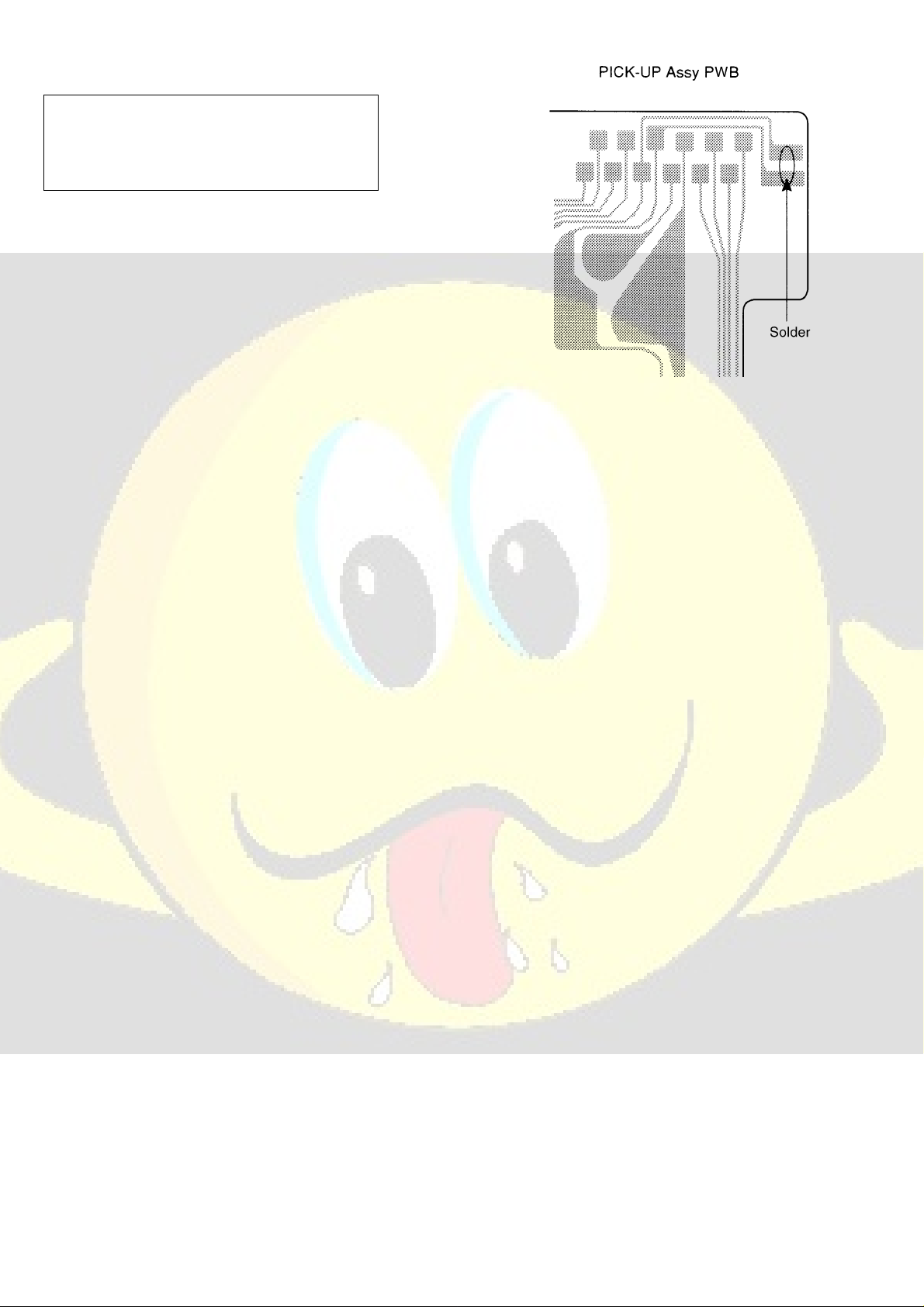
Precaution to replace Optical block
(KSS-213C)
Body or clothes electrostatic potential could ruin
laser diode in the optical block. Be sure ground
body and workbench, and use care the clothes
do not touch the diode.
1) After the connection, remove solder shown in
the right figure.
-4-
Page 5

ELECTRICAL MAIN PARTS LIST-1/4
REF. NO PART NO. KANRI DESCRIPTION
NO.
IC
87-A20-955-010 IC,LA1828
87-A21-193-010 IC,TA8227P
87-A21-443-040 C-IC,M62495AFP<A340KHC>
87-A22-139-040 C-IC,MM3072XJ<EXCEPT A340KHC>
87-A20-446-010 C-IC,LA9241ML
87-A21-319-010 C-IC,LC78622NE
87-A21-891-010 C-IC,MM1469XH
8B-CDL-600-010 C-IC,LC865516A
87-A21-431-010 IC,BA4560N
TRANSISTOR
89-327-143-080 TR,2SC2714 (0.1W)
87-026-447-080 TR,2SC1740S R
87-A30-216-080 TR,2SA933AS(R)<EXCEPT A340KHC>
87-026-463-080 TR,2SA933S (0.3W)<A340KHC>
87-A30-288-040 C-TR,DTC114YKA<EXCEPT A340KHC>
87-026-213-080 CHIP-TR,DTC114YK
89-327-125-080 CHIP TR,2SC2712GR
89-318-154-080 TR,2SC1815 (0.4W)
89-112-965-080 TR,2SA1296 (0.75W)
87-A30-623-080 TR,DTC124XSA
89-213-702-080 TR,2SB1370E
87-026-462-080 TR,2SC1740 S(RS 0.3W)
89-109-332-380 TR,2SA933RS
87-A30-515-080 TR,2SA1979O/Y
87-A30-287-040 C-TR,DTC114TKA
87-A30-435-040 C-TR,DTC144EK T146
89-317-403-080 TR,2SC1740S
87-A30-621-080 TR,DTC114TSA
87-026-239-080 TR,DTC114TK (0.2W)
87-026-464-080 TR,DTC114TS (0.3W)
DIODE
87-020-465-080 DIODE,1SS133 (110MA)
87-A40-916-040 C-VARI-CAP,HVC202A
87-027-703-080 ZENER,HZ7A1L (5MA)
87-A40-648-080 ZENER,MTZJ8.2A
87-A40-234-080 ZENER,MTZJ5.6A
87-017-978-080 DIODE,1N4003
87-027-702-080 DIODE,ZENER HZ6C2L (200MA)
87-A40-347-080 ZENER,MTZJ2.2B
87-A40-465-010 DIODE,FR202
TUNER C.B
C1 87-010-314-080 C-CAP,S 22P-50V
C3 87-010-314-080 C-CAP,S 22P-50V
C5 87-010-378-080 CAP, ELECT 10-16V
C7 87-012-156-080 C-CAP,S 220P-50 CH
C8 87-010-197-080 CAP,CHIP 0.01 DM
C10 87-010-197-080 CAP,CHIP 0.01 DM
C11 87-018-170-080 CAP,TC-U 8.2P-50 UJ
C12 87-010-314-080 C-CAP,S 22P-50V
C14 87-010-148-080 C-CAP,S 4P-50 C CH GRM
C15 87-016-669-080 C-CAP,S 0.1-25 K B
C16 87-010-178-080 CHIP CAP 1000P
C17 87-016-669-080 C-CAP,S 0.1-25 K B
C18 87-010-197-080 CAP,CHIP 0.01 DM<EXCEPT A340KHC>
C19 87-016-669-080 C-CAP,S 0.1-25 K B
C20 87-010-400-080 CAP, ELECT 0.47-50V
C21 87-010-403-080 CAP, ELECT 3.3-50V
C22 87-010-197-080 CAP,CHIP 0.01 DM
C24 87-010-426-080 C-CAP,S 0.012-25 B<EXCEPT A340KHC>
C25 87-010-426-080 C-CAP,S 0.012-25 B<EXCEPT A340KHC>
C26 87-012-358-080 C-CAP,S 0.47-10 F Z
REF. NO PART NO. KANRI DESCRIPTION
C27 87-012-358-080 C-CAP,S 0.47-10 F Z
C28 87-010-992-080 C-CAP,S 0.047-25 B
C29 87-010-992-080 C-CAP,S 0.047-25 B
C30 87-010-248-080 CAP, ELECT 220-10V
C30 87-010-260-080 CAP, ELECT 47-25V
C31 87-010-379-080 CAP, ELECT 22-16V
C32 87-010-197-080 CAP,CHIP 0.01 DM
C33 87-010-197-080 CAP,CHIP 0.01 DM
C34 87-010-197-080 CAP,CHIP 0.01 DM
C35 87-010-197-080 CAP,CHIP 0.01 DM
C36 87-010-263-080 CAP, ELECT 100-10V
C37 87-010-197-080 CAP,CHIP 0.01 DM
C40 87-018-166-080 CAP,TC U 3.9P-50 K UJ UP050<A340KHC>
C50 87-012-156-080 C-CAP,S 220P-50 CH
C51 87-010-197-080 CAP,CHIP 0.01 DM
C52 87-010-197-080 CAP, CHIP 0.01 DM
C56 87-018-170-080 CAP,TC-U 8.2P-50 UJ
CF1 87-A90-128-010 FLTR,AM IF CFAL-455
CN2 87-A60-116-010 CONN,6P H S2M-6WR
L2 87-A50-560-010 COIL,FM BPF(ACD)
L3 8B-CDB-630-010 BAR-ANT ASSY,MW2B-BCD<EXCEPT A340KHC>
L6 87-A50-337-010 COIL,AM OSC (TOKO)
L7 87-A50-579-010 COIL,AM IFT(ACD)
L8 87-A50-335-010 COIL,FM IFT (TOKO)
L9 87-A50-577-010 COIL,FM DET(ACD)
L10 87-005-849-080 COIL,10UH(CECS)
L17 87-A50-337-010 COIL,AM OSC(TOKO)
L402 87-003-097-080 COIL,1UH
PVC1 87-A91-635-010 TUN-CAP,20P-140P E-ACD(MITSUMI<A340KHC>
PVC1 87-A91-167-010 TUN-CAP,20P-160P FA-22125 N000
S1 87-A91-548-010 SW,SL-2-3 SK23E01G06<EXCEPT A340KHC>
S1 87-A91-549-010 SW,SL-6-4 SK64D01G06<A340KHC>
TC5 87-011-253-080 TRIMER,30P LAR<A340KHC>
TC6 87-011-254-080 TRIMER,20P LAR<A340KHC>
X401 87-A70-046-010 VIB,XTAL 16.934MHZ
BATT1 C.B
C901 87-A11-146-080 CAP,TC U 0.022-50 Z F
C902 87-A11-146-080 CAP,TC U 0.022-50 Z F
C903 87-A11-146-080 CAP,TC U 0.022-50 Z F
C904 87-A11-146-080 CAP,TC U 0.022-50 Z F
CNA901 8A-CD9-627-010 CONN ASSY,3P PWR
!
ICP901 87-A90-092-080 PROTECTOR,2.5A 491
!
J901 87-A61-455-010 JACK,AC E PSE27
SP901 87-CD6-213-010 SPR-C,BATT (-)
SP902 87-CD6-213-010 SPR-C,BATT (-)
BATT2 C.B
SP903 87-CD6-213-010 SPR-C,BATT (-)
SP904 87-CD6-213-010 SPR-C,BATT (-)
MAIN CD C.B
C251 87-010-404-080 CAP, ELECT 4.7-50V
C263 87-010-426-080 C-CAP,S 0.012-25 B
C264 87-010-426-080 C-CAP,S 0.012-25 B
C265 87-010-263-080 CAP, ELECT 100-10V
C266 87-010-263-080 CAP, ELECT 100-10V
C267 87-010-112-080 CAP, ELECT 100-16V
C268 87-010-112-080 CAP, ELECT 100-16V
C271 87-010-221-080 CAP, ELECT 470-10V
C272 87-010-221-080 CAP, ELECT 470-10V
C278 87-010-384-080 CAP, ELECT 100-25V
NO.
<EXCEPT A340KHC>
-5-
Page 6

ELECTRICAL MAIN PARTS LIST-2/4
REF. NO PART NO. KANRI DESCRIPTION
C279 87-010-385-080 CAP, ELECT 220-25V
!
C301 87-016-495-000 CAP,E 3300-25 M SMG
C306 87-010-404-080 CAP, ELECT 4.7-50V
C307 87-010-401-080 CAP, ELECT 1-50V
C308 87-010-221-080 CAP, ELECT 470-10V
C321 87-010-197-080 CAP, CHIP 0.01 DM
C322 87-010-263-080 CAP, ELECT 100-10V
C325 87-010-405-080 CAP, ELECT 10-50V
C401 87-010-403-080 CAP, ELECT 3.3-50V
C402 87-010-197-080 CAP, CHIP 0.01 DM
C403 87-010-263-080 CAP, ELECT 100-10V
C404 87-010-248-080 CAP, ELECT 220-10V
C405 87-010-197-080 CAP, CHIP 0.01 DM
C406 87-010-374-080 CAP, ELECT 47-10V
C407 87-018-131-080 CAP, CER 1000P-50V
C408 87-010-198-080 CAP, CHIP 0.022
C409 87-010-248-080 CAP, ELECT 220-10V
C410 87-010-263-080 CAP, ELECT 100-10V
C411 87-A11-177-080 C-CAP,S 0.15-16 K B
C412 87-010-401-080 CAP, ELECT 1-50V
C413 87-016-369-080 C-CAP,S 0.033-25 B K
C414 87-010-405-080 CAP, ELECT 10-50V
C416 87-010-545-080 CAP, ELECT 0.22-50V
C417 87-012-157-080 C-CAP,S 330P-50 CH
C418 87-010-213-080 C-CAP,S 0.015-50 B
C419 87-A11-608-080 C-CAP,S 0.33-25 K B
C420 87-016-369-080 C-CAP,S 0.033-25 B K
C421 87-A11-177-080 C-CAP,S 0.15-16 K B
C422 87-010-183-080 C-CAP,S 2700P-50 B
C423 87-010-992-080 C-CAP,S 0.047-25 B
C424 87-010-220-080 C-CAP,S 0.018-25 B
C425 87-018-129-080 CAP, CER 680P-50V
C426 87-A11-608-080 C-CAP,S 0.33-25 K B
C428 87-010-426-080 C-CAP,S 0.012-25 B
C429 87-010-186-080 CAP,CHIP 4700P
C430 87-012-156-080 C-CAP,S 220P-50 CH
C431 87-010-545-080 CAP, ELECT 0.22-50V
C432 87-010-374-080 CAP, ELECT 47-10V
C433 87-010-401-080 CAP, ELECT 1-50V
C434 87-010-184-080 CHIP CAPACITOR 3300P(K)
C435 87-010-197-080 CAP, CHIP 0.01 DM
C436 87-010-374-080 CAP, ELECT 47-10V
C437 87-010-404-080 CAP, ELECT 4.7-50V
C438 87-016-669-080 C-CAP,S 0.1-25 K B
C439 87-010-178-080 CHIP CAP 1000P
C440 87-018-139-080 CAP,TC-U 1P-50 CH
C441 87-010-197-080 CAP, CHIP 0.01 DM
C442 87-018-148-080 CAP,TC-U 12P-50 CH
C445 87-012-368-080 C-CAP,S 0.1-50 F
C446 87-012-368-080 C-CAP,S 0.1-50 F
C447 87-012-368-080 C-CAP,S 0.1-50 F
C448 87-010-315-080 C-CAP,S 27P-50 CH
C451 87-012-156-080 C-CAP,S 220P-50 CH
C455 87-010-247-080 CAP, ELECT 100-50V
C457 87-010-312-080 C-CAP,S 15P-50 CH
C458 87-010-312-080 C-CAP,S 15P-50 CH
C459 87-010-263-080 CAP, ELECT 100-10V
C460 87-015-819-080 CAPACITOR,0.01
C461 87-010-197-080 CAP, CHIP 0.01 DM
C462 87-010-248-080 CAP, ELECT 220-10V
C463 87-018-134-080 CAPACITOR,TC-U 0.01-16
C465 87-010-404-080 CAP, ELECT 4.7-50V
C466 87-012-368-080 C-CAP,S 0.1-50 F
C467 87-010-263-080 CAP, ELECT 100-10V
C469 87-012-154-080 C-CAP,S 150P-50 CH
NO.
REF. NO PART NO. KANRI DESCRIPTION
NO.
C471 87-018-209-080 CAP, CER 0.1-50V
C472 87-015-785-080 CHIP CAPACITOR, 0.1FZ-25Z
C473 87-015-785-080 CHIP CAPACITOR, 0.1FZ-25Z
C474 87-015-785-080 CHIP CAPACITOR, 0.1FZ-25Z
C475 87-018-134-080 CAPACITOR,TC-U 0.01-16
C476 87-010-236-080 CAP,E 1000-10 SME
C477 87-010-197-080 CAP, CHIP 0.01 DM
C478 87-010-263-080 CAP, ELECT 100-10V
C479 87-010-197-080 CAP, CHIP 0.01 DM
C480 87-010-221-080 CAP, ELECT 470-10V
C481 87-010-405-080 CAP, ELECT 10-50V
C482 87-010-405-080 CAP, ELECT 10-50V
C489 87-012-368-080 C-CAP,S 0.1-50 F
C490 87-012-368-080 C-CAP,S 0.1-50 F
C491 87-018-134-080 CAPACITOR,TC-U 0.01-16
C492 87-010-221-080 CAP, ELECT 470-10V
C493 87-010-180-080 C-CER 1500P
C501 87-012-368-080 C-CAP,S 0.1-50 F
C502 87-010-322-080 C-CAP,S 100P-50 CH
C503 87-018-119-080 CAP, CER 100P-50V
C504 87-010-322-080 C-CAP,S 100P-50 CH
C505 87-010-322-080 C-CAP,S 100P-50 CH
C506 87-010-322-080 C-CAP,S 100P-50 CH
C510 87-016-669-080 C-CAP,S 0.1-25 K B
C831 87-010-198-080 CAP, CHIP 0.022
CN202 8A-CH4-687-010 CONN,4P V 2.5
CN205 87-A60-109-010 CONN,2P V S2M-2W
CN301 8A-CH4-689-010 CONN,3P V 2.5
CN401 87-A60-424-010 CONN,16P V TOC-B
CN403 87-099-201-010 CONN,8P 6216 H
CN802 8A-CH4-687-010 CONN,4P V 2.5
CNA402 8A-CD9-625-010 CONN ASSY,6P CD-ME
J201 87-A60-420-010 JACK,3.5 ST (MSC)
L401 87-003-102-080 COIL, 10UH
L404 87-003-152-080 COIL, 100UH
SFR430 87-024-437-080 SFR100K,RH063EC
SW901 87-A90-146-010 SW,SL 1-1-2<EXCEPT A340KHC>
X601 87-030-273-010 VIB,XTAL 32.768K5PPM
MAIN TP C.B
C211 87-012-142-080 CAP, S 0.33-16
C212 87-012-142-080 CAP, S 0.33-16
C215 87-016-460-080 C-CAP,S 0.22-16 B
C216 87-016-460-080 C-CAP,S 0.22-16 B
C231 87-010-213-080 C-CAP,S 0.015-50 B
C232 87-010-213-080 C-CAP,S 0.015-50 B
C233 87-012-142-080 CAP, S 0.33-16
C234 87-012-142-080 CAP, S 0.33-16
C235 87-016-669-080 C-CAP,S 0.1-25 K B
C236 87-016-669-080 C-CAP,S 0.1-25 K B
C237 87-010-371-080 CAP, ELECT 470-6.3V
C239 87-010-197-080 CAP, CHIP 0.01 DM<EXCEPT A340KHC>
C240 87-010-197-080 CAP, CHIP 0.01 DM<EXCEPT A340KHC>
C247 87-010-401-080 CAP, ELECT 1-50V
C248 87-010-401-080 CAP, ELECT 1-50V
C310 87-010-248-080 CAP, ELECT 220-10V
C316 87-010-263-080 CAP, ELECT 100-10V
C317 87-015-819-080 CAPACITOR,0.01
C701 87-010-545-080 CAP, ELECT 0.22-50V
C702 87-010-400-080 CAP, ELECT 0.47-50V
C703 87-010-405-080 CAP, ELECT 10-50V
C704 87-010-248-080 CAP, ELECT 220-10V
C705 87-010-400-080 CAP, ELECT 0.47-50V
C707 87-010-401-080 CAP, ELECT 1-50V
C708 87-010-401-080 CAP, ELECT 1-50V
-6-
Page 7

ELECTRICAL MAIN PARTS LIST-3/4
REF. NO PART NO. KANRI DESCRIPTION
NO.
C801 87-010-248-080 CAP, ELECT 220-10V
C805 87-012-365-080 C-CAP,S 0.027-25VBK
C806 87-012-365-080 C-CAP,S 0.027-25VBK
C807 87-010-405-080 CAP, ELECT 10-50V
C808 87-010-405-080 CAP, ELECT 10-50V
C809 87-010-401-080 CAP, ELECT 1-50V
C810 87-010-401-080 CAP, ELECT 1-50V
C811 87-010-178-080 CHIP CAP 1000P
C812 87-010-178-080 CHIP CAP 1000P
C816 87-010-180-080 C-CER 1500P
C817 87-010-180-080 C-CER 1500P
C823 87-010-178-080 CHIP CAP 1000P
C824 87-010-178-080 CHIP CAP 1000P
C829 87-010-178-080 CHIP CAP 1000P
C830 87-010-178-080 CHIP CAP 1000P
C834 87-010-248-080 CAP, ELECT 220-10V
C843 87-018-134-080 CAPACITOR,TC-U 0.01-16
C844 87-018-124-080 CAP, CER 270P-50V
C845 87-010-178-080 CHIP CAP 1000P
C846 87-010-263-080 CAP, ELECT 100-10V
C851 87-018-133-080 CAPACITOR,CER 4700P-16V
C852 87-018-131-080 CAP, CER 1000P-50V
C853 87-A11-145-080 CAP,TC U 0.01-50 Z F
C889 87-010-196-080 CHIP CAPACITOR,0.1-25
CN201 87-099-757-010 CONN,16P 9604S F
CN701 87-A60-109-010 CONN,2P V S2M-2W
CN801 87-A60-110-010 CONN,4P V S2M-4W
CNA302 8A-CD9-629-010 CONN ASSY,6P MA-TU
L301 87-005-165-080 COIL 1UH (H,E)
L302 87-005-165-080 COIL 1UH (H,E)
L303 87-005-165-080 COIL 1UH (H,E)
L801 87-007-342-010 COIL,OSC 85K BIAS
SW801 8Z-CD9-609-010 SW,SL 1-6-2 PS62D01
FRONT C.B
C601 87-010-313-080 CAP, CHIP 18P
C602 87-010-315-080 C-CAP,S 27P-50 CH
C603 87-010-319-080 C-CAP,S 56P-50 CH
C604 87-010-317-010 CHIP CAP,S 39P CH
C605 87-010-264-040 CAP,E 100-10 5L
C606 87-015-785-080 CHIP CAPACITOR, 0.1FZ-25Z
C608 87-010-401-080 CAP, ELECT 1-50V
C609 87-010-400-080 CAP, ELECT 0.47-50V
C611 87-A10-189-040 CAP,E 220-10
C613 87-012-368-080 C-CAP,S 0.1-50 F
C614 87-010-312-080 C-CAP,S 15P-50 CH
C617 87-012-368-080 C-CAP,S 0.1-50 F
C618 87-018-209-080 CAP, CER 0.1-50V
C629 87-018-119-080 CAP, CER 100P-50V
C630 87-018-119-080 CAP, CER 100P-50V
REF. NO PART NO. KANRI DESCRIPTION
NO.
C631 87-018-119-080 CAP, CER 100P-50V
C632 87-018-119-080 CAP, CER 100P-50V
C638 87-010-197-080 CAP, CHIP 0.01 DM
CN601 87-099-757-010 CONN,16P 9604S F
CN602 87-099-201-010 CONN,8P 6216 H
CNA604 8B-CDB-616-010 CONN ASSY,3P V ORN KEY
L601 87-003-102-080 COIL, 10UH
L606 87-005-738-080 COIL,47UH J SP02
L608 87-003-097-080 COIL,1UH
L609 87-003-097-080 COIL,1UH
L611 87-003-097-080 COIL,1UH
LED601 8A-CDA-645-010 LED,6224-10ID RED
LED602 8A-CDA-645-010 LED,6224-10ID RED
LED603 8A-CDA-645-010 LED,6224-10ID RED
LED608 8A-CDA-645-010 LED,6224-10ID RED
LED610 8A-CDA-646-010 LED,6224-10GD GRN<EXCEPT A340KHC>
LED611 87-CD8-616-010 LED,SA36-11 HWA-11.0
S601 87-A91-704-080 SW,TACT EVQ 214 05R
S602 87-A91-704-080 SW,TACT EVQ 214 05R
S603 87-A91-704-080 SW,TACT EVQ 214 05R
S604 87-A91-704-080 SW,TACT EVQ 214 05R
S605 87-A91-704-080 SW,TACT EVQ 214 05R
S606 87-A91-704-080 SW,TACT EVQ 214 05R
S607 87-A91-704-080 SW,TACT EVQ 214 05R
S608 87-A91-704-080 SW,TACT EVQ 214 05R
X602 87-030-376-080 VIB,CER CSA5.76MG200
KEY C.B
CN605 8Z-CS3-621-010 CONN,3P LED
S609 87-A91-704-080 SW,TACT EVQ 214 05R
S611 87-A91-704-080 SW,TACT EVQ 214 05R
S614 87-A91-704-080 SW,TACT EVQ 214 05R
S615 87-A91-704-080 SW,TACT EVQ 214 05R
MOTOR C.B
M2 9X-262-576-910 MOTOR GEAR ASSY
PIN3 91-564-722-110 PIN CONN,6P
SW1 91-572-085-120 LEAF SW
-7-
Page 8
ELECTRICAL MAIN PARTS LIST-4/4
• Regarding connectors, they are not stocked as they are not the initial order items.
The connectors are available after they are supplied from connector manufacturers upon the order is received.
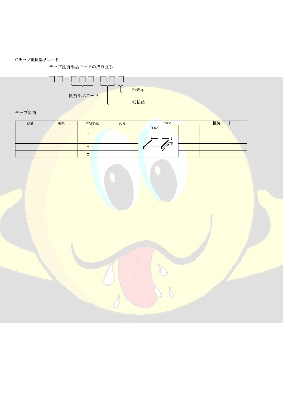
CHIP RESISTOR PART CODE
Chip Resistor Part Coding
88
A
Resistor Code
Chip resistor
Wattage Type Tolerance
1/16W 1005 5% CJ
1/16W
1/10W
1/8W
1608
2125
3216
5%
5%
5%
Symbol
CJ
CJ
CJ
Figure
Value of resistor
Form
L
Dimensions (mm)
t
W
0.55
Resistor Code
108
118
128
LW t
1.0 0.5 0.35 104
1.6 0.8 0.45
2 1.25 0.45
3.2
1.6
: A
: A
-8-
Page 9
IC BLOCK DIAGRAM-1/2
IC, BA4560N
IC, LA1828
FM
RF
IN
OUT R
GND
INF-R
FM
RF
OUT
VCC
IN-R
FM
OSC
GND
DET
OUT
IN-L
MPX
IN
INF-L
R
CH
OUT-L
L
CH
VCC
LPF1 LPF2 QUAD
AM
RF
IN
REF AM
OSC
VC
FM
MIX
GND AM
MIX
-9-
TU
LED
STIND
FM
IF
IN
AM
IF
IN
AGC
Page 10
IC BLOCK DIAGRAM-2/2
IC, M6249SAFP IC, MM3072CJ
IN1-R
IN2-R
IN3-R
IN4-R
RECOUT-R
SEND-R
RETUNR
TONE-H-R
TONE-L-R
OUT-R
GND
VDD
AUTO RESET
IN1-L
IN2-L
IN3-L
IN4-L
RECCOUNT-L
SEND-L
RETUNR-L
TONE-H-L
TONE-L-L
OUT-L
VSS
CONT
IN1-R
IN2-R
IN3-R
IN4-R
RECOUT-R
SEND-R
RETUNR
TONE-H-R
TONE-L-R
OUT-R
GND
VDD
1
2
3
4
5
6
7
8
9
10
11
VOL VOL
Treble
boost
Mono.SW
MUTE
ATT ATT
Bass
boost
Bass
boost
Control logic
Treble
boost
24
23
22
21
20
19
18
17
16
15
14
1312
IN1-L
IN2-L
IN3-L
IN4-L
RECCOUNT-L
SEND-L
RETUNR-L
TONE-H-L
TONE-L-L
OUT-L
VSS
CONT
IC, MM1469XH
SUBGND
-
IN-AIN
+
BIAS VCC VCC IN-B IN-A + -
-B
28 27 26 25 24 23 22
10k
13k
Level shift
10k
T.S.D
10k
Level shift
13k
10k
1 2 3 4 5 6 7
+
-
IN-AIN-BREQ-BREQ-OMUTE GND IN-B IN-A
Vcc
21 20 19 18 17 16 15
10k
Vcc
13k
Level shift
50k
DRIVER MUTE
50k
Level shift
13k
10k
8 9 10 11 12 13 14
+-
OPIN+
SUBGND
OPIN-
OPOUT
-10-
Page 11

WIRING-1/6 (MAIN/MOTOR)
101112131415161718192021222324
1234567892526272829303132
MAIN-CD C.B
(INSERTED PARTS)
1
6
CD DOOR
SW
A
8
7
FRONT C.B
CN602
J201
PHONES( )
1
4
1
3
BATT1 C.B
CNA901
MSJ-2000
MAIN SP
7Ω 3W
1
2
3
4
SP1
(R-CH)
SP2
(L-CH)
NOTE
B
C
D
E
12
2
1
2
1
F
E
C
B
6
7 9 10 12
1134
RXX
CXX
CXX
ECB
ECB
G
H
I
TO CD MECHANISM
KSM-213CDM
ECB
1
2
4
15
16
TAPE MECHANISM
ZZM-1 AR2NC
4
1
M1
–
(TAPE MOTOR)
+
S1
(TAPE SW)
J
K
L
MOTOR C.B
(CONDUCTOR SIDE)
SW801
PB
1
6
2
1
1
8
16
2
1
15
6
5
4
3
2
1
4
1
REC
4
3
2
TO DECK
CHASSIS
RPH
L
MECHANISM
R
EH
3
TAPE
ZZM-1
AR2NC
3
M
N
O
P
Q
R
S
MAIN-TP C.B
(INSERTED PARTS)
TUNER C.B
CN002
FRONT C.B
CN601
T
1
2
MIC
U
-11-
Page 12
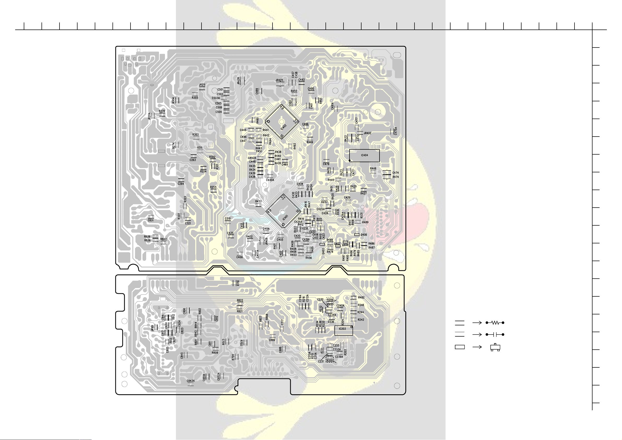
WIRING-2/6 (MAIN)
101112131415161718192021222324
1234567892526272829303132
MAIN-CD C.B
(CHIP PARTS)
64
15212228
17 814
A
B
C
D
E
F
G
H
I
K
12
13 24
J
K
L
M
N
O
NOTE
RXXX
1
CXXX
QXXX
P
Q
R
MAIN-TP C.B
(CHIP PARTS)
-12-
ECB
K
S
T
U
Page 13
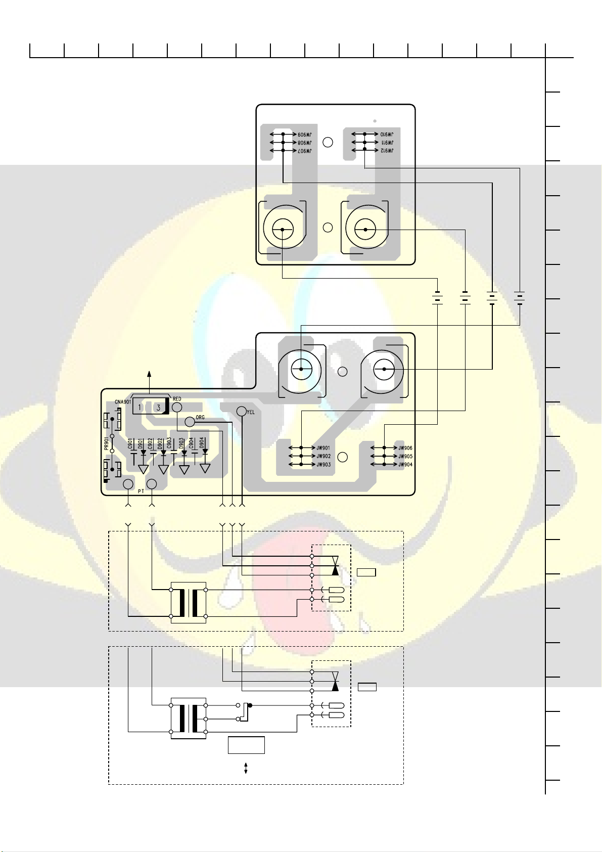
WIRING-3/6 (BATT1/BATT2)
123456789101112131415
BATT 1 C.B
(INSERTED PARTS)
MAIN-CD C.B
CN301
BATT 2 C.B
(INSERTED PARTS)
+
SP904
–
SP903
SP901
SP902
A
B
C
D
E
F
G
DRY BATTERY
R14P x 8
DC 12V
H
I
–
J
A340 K
MODEL
A360 HRJ, HS
MODEL
RED
RED
PT901
PT901
RED
YEL
ORG
SW901
AC
DC
AC
DC
+
J901
AC~
230V/50Hz
J901
AC~
110-120V
220-240V
50/60Hz
K
L
M
N
O
P
Q
R
S
VOLT AGE
SELECT
220-240V
110-110V
T
U
-13-
Page 14

SCHEMATIC DIAGRAM-1/5 (MAIN-TP/MAIN-CD2/2)
MIC
FRONT C.B CN601
TUNER C.B CN002
MAIN-TP C.B
CN701
R341
C889
0.1
MIC AMP
HRJ, HS MODEL K MODEL
C239, 240
R203, 204
R205, 206 NW
IC203
W/Q-SOUND W/O-SOUND
0.01
JR
MM3072XJ
MIC AGC
L301
L303
L302
MIC AGC
1µ
4.7K
1.2K
M62495AFP
MAIN-CD C.B
(2/2)
*
*
*
*
*
*
*
+5V REG
P
POWER AMP
A1
A2
A3
A4
A5
MAIN-CD C.B (1/2)
MAIN SP
7Ω 3W
SP1 (RCH)
SP2 (LCH)
J201
PHONES( )
MSJ-2000
Q243,244
MUTE
2.5
HRJ, HS MODEL
SW901
AC~
AC 110-120V
AC 220-240V
50/60Hz
J901
SW901
JR
VOLTAGE
SELECT
PT901
220-240V
110-120V
K MODEL
AC~
RPH
L
R
EH
TAPE
MECHANISM
ZZM-1 AR2NC
HEAD AZIMUTH
ADJ
CNA801
TO DECK
CHASSIS
SW801 1-6
(REC/PB SW)
SW801
PS62Q01
EQ AMP
L801
REC BIAS FREQ ADJ
Q810
DTC114TS
BEAT SW
5V REG
1SS133
PT901
Q301-303
Q304,305
1SS133
J901
AC 230V,50Hz
BATT1 C.B
5.6K
5.6K
4.7/50V
HZ6C2L
Q801
BIAS OSC
R
1SS1331SS133
OPE IND
Q841
DTC124XS
REC SW
HZ7A1L
100
1SS133
100
R
SIGNAL : NM : NO MOUNT
1SS133
1SS133
CONN, 4PV 2-5
CNA802
M1
(TAPE MOTOR)
M
S1
(TAPE SW)
TAPE MECHANISM ZZM-1 AR2NC
R
Q303
DTC124XS
PB/FM
REC/AM
C901 0.022
D901 FR202
C903 0.022
D903 FR202
D904 FR202
PWR
D902 FR202
CNA901
CONN ASSY.3P
SP901 SP902
491SERIES
C904 0.022
C902 0.022
SP904 SP903
BATT2 C.B
ICP901
2.5A
60V
DRY BATTERY
R14PX8
DC 12V
AC
DC
J901
AC~
-14-
Page 15

SCHEMATIC DIAGRAM-2/5 (MAIN-CD1/2)
MAIN-CD C.B (1/2)
LD CONT
Q406-408
RW SW
820
R
R
CD MECHANISM
KSM-213CDM
RW SW
R
820
R
LC78622NE
IMF
C469
150P
FRONT C.B CN602
OPTICAL
PICK UP
KSS-213C
MOTOR
C.B
M3
M2
SW1
2SA19790/Y
REG
SIGNAL :
PB (DIGITAL) PB (ANALOG)
CD +B SW
R
CD +B SW
A1
A2
A3
A4
A5
S-2M 2W
MAIN-CD C.B (2/2)
-15-
Page 16

WIRING-4/6 (FROTN/KEY)
101112131415161718192021222324
1234567892526272829303132
FRONT C.B (INSERTED PARTS)
CN201
MAIN-CD C.B
16
A
LED602
REPEAT
1
2
15
HRJ, HS MODEL
LED610
QSOUND
HRJ, HS
MODEL
LED611
TRACK
VOLUME/3-MODE
6
10
5
1
1
2
7
8
1
3
CNA604
CN403
MAIN- CD C.B
KEY C.B
(INSERTED PARTS)
13
HRJ, HS MODEL
S609
QSOUND
S611
3-MODE EQ
S615
VOL UP ( )
B
C
D
E
F
G
H
I
S603
SKIP/SEARCH
( )
S604
SKIP/SEARCH
( )
13
24
25
S601
REPEAT SLEEP/OSC
LED608
STANDBY
OPE/BATT
S608
TAPE/POWER
STANDBY
12
1
48
HRJ, HS
MODEL
LED601
RADIO
S607
RADIO
LED603
CD
S606
CD
S605
PLAY/PAUSE
( )
S602
STOP/MEMORY
( )
NOTE
CXX
RXX
RXX
QXX
EECCB
S614
VOL DOWN ( )
B
ECB
J
K
L
M
N
O
P
Q
R
S
37
36
FRONT C.B (CHIP PARTS)
-16-
ECB
T
U
Page 17

SCHEMATIC DIAGRAM-3/5 (FRONT)
FRONT C.B
STANDBY
OPE/BATT
MAIN-TP C.B CN201 MAIN-CD C.B (1/2) CN403
CONN, 8P 6216H
R653 1K
0.1
0.01
SYSTEM
CONTROL
KHz
SFT LED
R
CLK-SHIFT SW
0.01
HRJ, HS MODEL
LED SW
RR
LED SW
HRJ, HS
MODEL
HRJ, HS MODEL
R
RADIO
CD
Q606,607
LED SW
REPEAT
KEY C.B
CNA604
CONN ASSY 3P
22
CN605
CONN3P
CONN 16P 9604SF
DIGIT SW
R
LED611 SA36-11 HWA-11-0
TRACK
VOLUME/3-MODE EQ
DTC114YK
R
RESET
S601~609, 611,614, 615
SW, TACT EVQ 214 05R
S601 REPEAT SLEEP/OSC
S602 STOP/MEMORY ( )
S603 SKIP/SEARCH ( )
S604 SKIP/SEARCH ( )
S605 PLAY/PAUSE ( )
S606 CD
S607 RADIO
S608 TAPE/POWER STANDBY
S609 QSOUND
S611 3-MODE EQ
S614 VOL DOWN ( )
S615 VOL UP ( )
31
HRJ, HS
MODEL
13
-17-
Page 18

WIRING-5/6 (TUNER : K)
TUNER C.B (INSERTED PARTS)
123456789101112131415
A
B
C
L003
BAR ANT
FM ROD
ANT
TC004
TC002 TC001
TC003
16
MAIN-TP C.B
CNA302
1
2
56
343
1
2
34
343
1
2
21
343
1
2
4
1
2
4
1
2
4
SW001
BAND
1
FM (ST) MW LW
FM
(MONO)
D
E
F
G
234
H
I
J
K
L
TUNER C.B (CHIP PARTS)
NOTE
RXXX
RXXX
CXX
CXXX
ECB
ECB
M
N
O
P
Q
R
S
T
U
-18-
Page 19

SCHEMATIC DIAGRAM-4/5 (TUNER : K)
PVC1 E-ACD
FM BALANCE ADJ.
FM OSC
6800p
FM BPF
3.9
6800p
C050
220p
6800p
D005
1SS133
R052
100k
R050
12k
Q050
R051
2SC2712GR
47k
180
Q50
FM SW
MAIN-TP C.B
C052
0.01
-19-
Page 20

WIRING-6/6 (TUNER : HS, HRJ)
123456789101112131415
A
L003
BAR ANT
FM ROD
ANT
TUNER C.B
CN003
CN004
CN005
CN006
(INSERTED PARTS)
TC004
TC002 TC001
TC003
16
1
-1 -2
2
1
2
3
3
SW001
BAND
23
1
FM (ST) AM
FM
(MONO)
B
C
D
E
F
G
H
I
J
TUNER C.B
(CHIP PARTS)
MAIN-TP C.B
CNA302
NOTE
RXXX
RXXX
CXX
CXXX
ECB
ECB
K
L
M
N
O
P
Q
R
S
-20-
T
U
Page 21

SCHEMATIC DIAGRAM-5/5 (TUNER : HS, HRJ)
FM OSC
SH001
PVC1 FA-22125
FM BPF
L005, TC001
FM FREQ. RANGE
ADJ.
C050 220p
D005
1SS133
R052
100k
R050
12k
Q050
2SC2712GR
R051
47k
Q50
FM SW
6PH 52M-6WR
C052
0.01
MAIN-TP C.B
-21-
Page 22

TRANSISTOR ILLUSTRATION-1/1
ECB ECB ECB
2SA1296
2SC1815
C
B
E
2SC2712
2SC2714
DTC114TK
DTC114YK
DTC144EK
2SA933
2SC1740
DTC114TS
DTC124XS
BCE
2SB1370
2SA1979
-22-
Page 23

VOLTAGE CHART-1/4
IC404 MM1469XH
PIN
123456789101112
ACTIVE
STATIC
ACTIVE
STATIC
ACTIVE
STATIC
4.2 4.2 2.95 2.95 8.2 5.8 5.8 0 2.95 3.00 4.27 4.01
3.61 3.62 2.54 2.54 7.24 5.02 5.02 0 2.55 2.55 3.61 3.63
PIN
13 14 15 16 17 18 19 20 21 22 23 24
0 8.40 1.45 1.45 4.10 4.10 2.90 2.90 8.90 8.90 2.90 2.90
0 7.39 0.78 0.8 3.63 3.62 2.54 2.55 7.96 7.96 2.55 2.55
PIN
25 26 27 28
2.90 4.50 3.71 0
2.54 3.61 3.62 0
IC402 LC78622NE
PIN
123456789101112
ACTIVE
STATIC
ACTIVE
STATIC
ACTIVE
STATIC
ACTIVE
STATIC
ACTIVE
STATIC
ACTIVE
STATIC
0 0 1.8 0 2.1 5.6 0.4 0 2.8 2.7 0 0.3
0 0 0.01 0 1.85 4.98 0.07 0 2.52 2.41 0 0
PIN
13 14 15 16 17 18 19 20 21 22 23 24
0 0 0 1.5 0 5.6 0 0 2.7 5.6 5.6 0
0 5 0.01 0.04 5.01 5.01 0 0 2.48 0 5.02 0
PIN
25 26 27 28 29 30 31 32 33 34 35 36
0 0 5.6 0 0 0 2.8 0 0 0 0 5.3
055004.952.480005.024.77
PIN
37 38 39 40 41 42 43 44 45 46 47 48
2.15 0 0 2.15 5.3 0 5.5 2.3 2.3 2.3 0.1 0
1.94 0 0 1.95 4.77 5 5.02 2.08 2.06 0 0.08 2.27
PIN
49 50 51 52 53 54 55 56 57 58 59 60
0.1 2.77 0 2.77 0.9 0 0 5.16 5 5.5 0 2.25
0 2.50 0 2.50 0 0.07 0 4.71 4.71 5 0 2.02
PIN
61 62 63 64
2.66 0 0 0
2.41 0 0 0
IC401 LA9241ML
PIN
123456789101112
ACTIVE
STATIC
ACTIVE
STATIC
ACTIVE
STATIC
ACTIVE
STATIC
ACTIVE
STATIC
ACTIVE
STATIC
2.67 2.65 2.67 2.67 2.67 2.66 2.67 2.67 2.65 2.66 2.67 2.7
2.53 2.53 2.53 2.56 2.53 2.55 2.55 2.55 2.54 2.52 2.55 2.54
PIN
13 14 15 16 17 18 19 20 21 22 23 24
2.67 2.7 2.72 2.69 2.67 2.69 2.73 2.69 0 2.67 2.67 2.65
2.55 2.54 2.54 2.54 2.55 2.55 2.54 2.54 2.54 0 2.53 2.54
PIN
25 26 27 28 29 30 31 32 33 34 35 36
2.69 2.75 2.75 2.68 2.75 2.45 2.45 0 0 5.22 0 1.4
2.56 2.56 2.5 2.55 2.55 2.33 2.34 0 0 5.01 5.01 0.04
PIN
37 38 39 40 41 42 43 44 45 46 47 48
0 0 0 0.25 2.45 2.54 2.54 2.63 0 2.64 2.65 0
0.01 5 0 0 1.61 2.45 2.41 2.53 0 2.54 2.55 0
PIN
49 50 51 52 53 54 55 56 57 58 59 60
0 2.54 4.77 4.86 0 5.11 0.16 5.2 2.64 2.64 2.59 2.57
0 2.44 4.71 4.71 0.07 0.03 0.14 5.01 2.54 2.56 0.98 0.99
PIN
61 62 63 64
2.3 3.86 0.19 5.18
2.24 4.35 0 5.02
-23-
Page 24

VOLTAGE CHART-2/4
IC203 M62495AFP, M61509FP
PIN
CD
TAPE
TUNER
PIN
CD
TAPE
TUNER
1234567891011 12
2.54 2.55 2.55 0.7 2.54 2.56 2.55 2.55 2.55 2.55 2.56 5.08
2.55 2.55 2.55 0.8 2.55 2.56 2.55 2.56 2.55 2.55 2.56 5.09
2.56 2.56 2.56 2.56 2.57 2.57 2.57 2.57 2.56 2.57 2.57 5.11
13 14 15 16 17 18 19 20 21 22 23 24
2.82 0 2.55 2.55 2.55 2.55 2.57 2.54 0.7 2.54 2.55 2.54
2.83 0 2.55 2.55 2.56 2.55 2.57 2.55 0.58 2.06 2.56 2.55
2.83 0 2.56 2.56 2.57 2.56 2.58 2.57 0.69 2.56 2.56 2.56
IC001 LA1828
PIN
123456789101112
FM
AM
FM
AM
0.93 0 4.73 4.73 4.68 1.28 1.24 1.35 1.35 4.22 0.01 4.80
0 0 4.88 4.88 4.88 0.28 1.24 1.36 1.36 0 3.20 4.88
PIN
13 14 15 16 17 18 19 20 21 22 23 24
0.59 1.27 1.27 0 5.30 4.80 0.01 4.80 4.80 4.80 1.28 0.33
0.30 1.25 1.25 0 5.30 4.88 0 4.88 4.88 4.88 1.26 1.26
IC801 BA4560N
PIN
12345678
TAPE
REC
3.37 3.37 3.34 0 3.34 3.37 3.37 6.83
3.38 3.39 3.35 0 3.35 3.39 3.38 6.82
IC202 TA8227
PIN
123456789101112
ACTIVE
STATIC
12.31 6.57 12.00 0 0.56 0 0 0.56 6.65 12.00 6.46 13.10
11.50 6.10 1.50 0 0.56 0 0 0.56 6.41 1.42 6.20 12.50
-24-
Page 25

VOLTAGE CHART-3/4
IC601 LC865516A
PIN
123456789101112
TAPE
TUNER
CD
TAPE
TUNER
CD
TAPE
TUNER
TAPE
TUNER
CD
0.12 0.12 0.12 0.07 4.65 1.59 0 2.52 0 2.11 2.25 4.8
0.12 0.11 0.11 0.03 4.7 1.64 0 2.58 0.02 4.40 4.9 4.9
0.10 0.09 8.53 0.26 4.61 1.58 0 2.49 0 2.09 2.23 4.76
PIN
13 14 15 16 17 18 19 20 21 22 23 24
4.99 4.99 0.9 0 0.03 1.2 4.8 0.03 5.23 0 0.04 0
5.1 5.1 5.1 0 0.02 0 4.9 0.03 5.34 0 0.05 0
5.06 5.06 5.07 4.84 0 0 4.76 0.01 5.2 0.01 0.01 0
PIN
25 26 27 28 29 30 31 32 33 34 35 36
4.77 0.06 0.06 4.76 0 0.06 0.06 0.26 0.07 0.05 0.08 0.05
4.86 0.05 4.9 4.87 0.06 0.06 0.06 0.16 0.06 0.05 0.09 0.05
4.74 4.75 0.04 4.71 0 0.04 0 0.24 0.04 4.75 1.94 4.75
CD
PIN
37 38 39 40 41 42 43 44 45 46 47 48
0.05 0.06 0.05 0.05 4.79 0.34 9.54 0.12 9.55 0.12 0.12 2.3
0.05 0.06 0.05 4.86 0.05 2.82 9.44 0.12 9.11 0.12 0.12 2.3
0.03 0.04 4.72 0.03 0.03 2.39 6.11 0.1 0.11 0.1 0.1 2.2
NO. Q002 Q003 Q004
PIN e c b e c b e c b
FM
AM
4.82 8.00 5.52 5.53 5.52 4.85 0 4.06 2.98
4.90 8.00 5.58 5.59 5.59 4.90 2.30 4.12 3.03
NO. Q001
PIN e c b
FM
AM
2.22 4.07 2.95
2.21 4.06 2.95
NO. Q403 Q406 Q407 Q408
PINecbecbecbecb
ACTIVE
STATIC
2.56 2.56 0 0 4.6 0 4.6 2.57 2.56 4.6 2.57 2.56
2.56 2.56 0 0 4.6 0 4.58 2.55 2.55 4.58 .55 2.55
NO. Q401 Q402 Q491 Q492
PINecbecbecbecb
ACTIVE
STATIC
4.46 2.11 3.76 7.87 5.3 7.17 7.91 7.88 7.15 0 0.14 4.41
4.99 1.56 4.35 7.97 5.15 7.28 7.98 7.97 7.23 0 0.14 4.41
NO. Q310 Q301 Q302 Q303
PINecbecbecbecb
ACTIVE
STATIC
5.55 10.45 6.25 12.2 11.4 11.5 11.5 11.4 10.9 0 0 4.57
5.56 10.83 6.26 12.66 12 11.99 11.99 12 11.32 0 0 4.57
NO. Q305 Q244 Q243 Q321
PINecbecbecbecb
ACTIVE
STATIC
7.23 10.56 7.85 0 0 0.12 0 0 0.12 0 0.01 0.6
7.26 11.23 7.87 0 0 0.64 0 0 0.64 0 0.02 0.7
-25-
Page 26

VOLTAGE CHART-4/4
NO. Q306 Q304
PIN e c b e c b
ACTIVE
STATIC
5.08 7.94 10.75 11.38 7.94 10.75
5.09 7.98 5.81 11.97 7.98 11.34
NO. Q841 Q810 Q801 Q701
PINecbecbecbecb
TAPE
REC
0 0.72 0 3.36 0.05 0.13 0 0 0 0 0 0
0 0.01 5.73 3.38 13.85 0.13 1.64 5.90 2.31 0.14 1.15 0.78
NO. Q702 Q703
PIN e c b e c b
TAPE
REC
000000
0 0.03 0.17 0.04 5.58 0.05
NO. Q606 Q604 Q607
PIN e c b e c b e c b
TAPE
TUNER
CD
0.02 6.56 0.05 0.02 6.51 0.06 0.02 6.55 0.05
0.02 0.04 4.46 0.02 6.51 0.06 0.02 6.54 0.05
0.02 6.55 0.06 0.02 6.51 0.07 0.02 0.05 4.35
-26-
Page 27

ELECTRICAL ADJUSTMENT-1/2
TUNER C.B
(PARTS SIDE)
2
L004
5
(HRJ, HS MODEL)
TC004
L003
(BAR ANT)
1
L007
TC003
TC001
19
IC001
L006
L005
L009
PVC1
TC002
L008
63 74
MAIN-CD C.B
(PARTS SIDE)
234
TUNER C.B
21
L003
(BAR ANT)
(PARTS SIDE)
4
TC006
3
7
PVC1
TC004
L004
TC002
L008
(K MODEL)
L007
TC003
TC001
19
IC001
L016 L017
L005
TC005
L009
85 96
0!
J201
PHONES
IC404
SFR430
#
CN401
MAIN-TP C.B
(PARTS SIDE)
20
IC401
58
IC801
1
CN201
M1 (TAPE MOTOR)
L801
@
CN801
6
4
RPH
-27-
0
!
Page 28

ELECTRICAL ADJUSTMENT-2/2
< TUNER SECTION >
(HRJ, HS MODEL)
1. AM Frequency Range Adjustment
L006 ....................................................................... 515kHz
TC003................................................................... 1650kHz
2. AM Tracking Adjustment
L003 ....................................................................... 600kHz
TC004................................................................... 1400kHz
3. AM IF Adjustment
Settings: • Test point: IC001 (LA1828) 19PIN
• Adjustment location: L007
Method: Adjust L007 so that the output level at 465kHz
becomes maximum.
4. FM Frequency Range Adjustment
L005 .....................................................................87.0MHz
TC001.................................................................109.0MHz
5. FM Tracking Adjustment
L004 .....................................................................90.0MHz
TC002.................................................................106.0MHz
6. FM IF Adjustment
Settings: • Test point: IC001 (LA1828) 19PIN
• Adjustment location: L008
Method: Adjust L008 so that the output level at 10.7MHz
becomes balanced.
7. FM Balance Adjustment
Settings: • Test point: IC001 (LA1828) 19PIN
• Adjustment location: L009
Method: Adjust L009 so that the output level at 10.7MHz
becomes balanced.
(K MODEL)
1. MW Frequency Range Adjustment
L016 ....................................................................... 515kHz
TC005..................................................................... 295kHz
2. LW Frequency Range Adjustment
L017 ....................................................................... 145kHz
TC003................................................................... 1635kHz
3. MW Tracking Adjustment
L003 ....................................................................... 600kHz
TC004................................................................... 1400kHz
7. FM Tracking Adjustment
L004 ........................................................................ 90MHz
TC002.................................................................... 106MHz
8. FM IF Adjustment
Settings: • Test point: IC001 (LA1828) 19PIN
• Adjustment location: L008
Method: Adjust L008 so that the output level at 10.7MHz
becomes balanced.
9. FM Balance Adjustment
Settings: • Test point: IC001 (LA1828) 19PIN
• Adjustment location: L009
Method: Adjust L009 so that the output level at 10.7MHz
becomes balanced.
< DECK SECTION >
10. Tape Speed Adjustment
Settings : • Test tape : TTA–100
• Test point : J201 (PHONES jack)
• Adjustment location : SFR of deck motor
Method : Play back the test tape and adjust SFR so that the
frequency counter reads 3000Hz +90Hz, -60Hz.
11. Head Azimuth Adjustment
Settings : • Test tape : TTA–320
• Test point : J201 (PHONES jack)
• Adjustment location : Azimuth adjustment
screw
Method : Play back the 8kHz signal of the test tape and adjust
screw so that the output becomes maximum.
12. Rec Bias frequncy Adjustment
Settings : • Test tape : TTA–602
• Test point : 6PIN, 4PIN (L801)
• Adjustment location : L801
L801..................................................................85kHz±2kHz(Recording)
< CD SECTION >
13. Focus Bias Adjustment
Settings : • Test point : IC401 PIN58 (VR), IC401 PIN 20
(FE)
• Adjustment location : SFR430
Method : Playback the disc and adjust SFR430 so that the test
point voltage becomes 0~-10mV.
4. LW Tracking Adjustment
L003 ....................................................................... 160kHz
TC006..................................................................... 288kHz
5. AM IF Adjustment
Settings: • Test point: IC001 (LA1828) 19PIN
• Adjustment location: L007
Method: Adjust L007 so that the output level at 465kHz
becomes maximum.
6. FM Frequency Range Adjustment
L005 ...................................................................87.35MHz
TC001...............................................................108.25MHz
-28-
Page 29

IC DESCRIPTION-1/3 (LA9241ML)-1/2
Pin No. Pin Name I/O Description
Pin to which external pickup photo diode is connected. RF signal is created by adding with the
1
2
FIN2
FIN1
I
FIN1 pin signal. FE signal is created by subtracting from the FIN1 pin signal.
I
Pin to which external pickup photo diode is connected.
10
11
12
13
14
15
16
17
3
4
5
6
7
8
9
E
F
TB
TE-
TE
TESI
SCI
TH
TA
TD-
TD
JP
TO
FD
FD-
Pin to which external pickup photo diode is connected. TE signal is created by subtracting from
I
the F pin signal.
I
Pin to which external pickup photo diode is connected.
I
DC component of the TE signal is input.
I
Pin to which external resistor setting the TE signal gain is connected between the TE pin.
O
TE signal output pin.
TES “Track Error Sense” comparator input pin. TE signal is passed through a band-pass filter
I
then input.
I
Shock detection signal input pin.
I
Tracking gain time constant setting pin.
O
TA amplifier output pin.
Pin to which external tracking phase compensation constants are connected between the TD and
I
VR pins.
I
Tracking phase compensation setting pin.
I
Tracking jump signal (kick pulse) amplitude setting pin.
O
Tracking control signal output pin.
O
Focusing control signal output pin.
Pin to which external focusing phase compensation constants are connected between the FD and
I
FA pins.
18
19
20
21
22
23
24
25
26
27
28
29
30, 31
32, 33
34
FA
FA-
FE
FE-
AGND
SP
SPI
SPG
SP-
SPD
SLEQ
SLD
SL-, SL+
JP-, JP+
TGL
—
Pin to which external focusing phase compensation constants are connected between the FD–
I
and FA– pins.
Pin to which external focusing phase compensation constants are connected between the FA and
I
FE pins.
O
FE signal output pin.
I
Pin to which external FE signal gain setting resistor is connected between the FE pin.
Analog signal GND.
O
Signal ended output of the CV+and CV- pin input signal.
I
Spndle amp input.
I
Pin to which external spindle gain setting resistor in 12 cm mode is connected. (Not connected)
Pin to which external spindle phase compensation constants are connected together with SPD
I
pin.
O
Spindle control signal output pin.
I
Pin to which external sled phase compensation constants are connected.
O
Sled control signal output pin.
I
Sled advance signal input pin from microprocessor.
I
Tracking jump signal input pin from DSP.
I
Tracking gain control signal input from DSP. Low gain when TGL = H.
35
TOFF
I
Tracking off control signal input pin from DSP. Off when TOFF = H.
-29-
Page 30

IC DESCRIPTION-1/3 (LA9241ML)-2/2
Pin No. Pin Name I/O Description
36
TES
O
Pin from which TES signal is output to DSP.
37
38
39, 40
41
42
43
44
45
46
47
48
49
50
51
52
53
HFL
SLOF
CV-, CV+
RFSM
RFS-
SLC
SLI
DGND
FSC
TBC
NC
DEF
CLK
CL
DAT
CE
O
O
O
—
O
—
O
“High Frequency Level” is used to judge whether the main beam position is on top of bit or on
top of mirror.
I
Sled servo off control input pin.
I
CLV error signal input pin from DSP.
RF output pin.
I
RF gain setting and EFM signal 3T compensation constant setting pin together with RFSM pin.
“Slice Level Control” is the output pin which controls the RF signal data slice level by DSP.
I
Input pin which control the data slice level by the DSP.
Digital system GND.
Output pin to which external focus search smoothing capacitor is connected.
I
“Tracking Balance Control” EF balance variable range setting pin.
Not connected.
Disc defect detector output pin.
I
Reference clock input pin. 4.23 MHz of the DSP is input.
I
Microprocessor command clock input pin.
I
Microprocessor command data input pin.
I
Microprocessor command chip enable input pin.
54
55
56
57
58
59
60
61
62
63
64
DRF
FSS
VCC2
REFI
VR
LF2
PH1
BH1
LDD
LDS
VCC1
—
—
—
O
“Detect RF” RF level detector output.
I
“Focus Search Select” focus search mode (± search/+ search) select pin. (Not connected)
Servo system and digital system Vcc pin.
Pin to which external bypass capacitor for reference voltage is connected.
O
Reference voltage output pin.
I
Disc defect detector time constant setting pin.
I
Pin to which external capacitor for RF signal peak holding is connected.
I
Pin to which external capacitor for RF signal bottom holding is connected.
O
APC circuit output pin.
I
APC circuit input pin.
RF system Vcc pin.
-30-
Page 31

IC DESCRIPTION-2/3 (LC78622NE)-1/2
Pin No. Pin Name I/O Description
1
2
3
DEFI
TAI
PDO
I
Defect sense signal (DEF) input pin. (Connect to 0V when not used).
I
O
Test signal input pin with built-in pull-down resistor. Be sure to connect to 0V.
Phase comparator output pin to control external VCO.
4
5
6
7
8
9
10
11
12, 13
14
15
16
17
18
19, 20
21
VVSS
ISET
VVDD
FR
VSS
EFMO
EFMIN
T2
CLV+, CLK-
V/P
HFL
TES
TOFF
TOL
JP+, JP-
PCK
—
—
—
For PLL.
I
I
Digital system GND. Be sure to connect to 0V.
O
For slice level control.
I
I
Test signal input pin with built-in pull-down resistor. Be sure to connect to 0V.
O
Disc motor control output. Three level output is possible using command.
Rough servo or phase control automatic selection monitoring output pin. Rough servo at H.
O
Phase servo at L.
I
Track detect signal input pin. Schmidt input.
I
Tracking error signal input pin. Schmidt input.
O
Tracking OFF output pin.
O
Tracking gain selection output pin. Gain boost at L.
O
Track jump control signal output pin. Three level output is possible using command.
O
EFM data playback clock monitoring pin 4.3218 MHz when phase is locked in. (Not connected)
GND pin for built-in VCO. Be sure to connect to 0V.
Pin to which external resistor adjusting the PD0 output current.
Power supply pin for built-in VCO.
Pin for VCO frequency range adjustment.
EFM signal output pin.
EFM signal input pin.
22
23
24
25
26
27
28
29
30
31
32, 33
34
35
36
37
38
39
40
41
42
FSEQ
VDD
SL+
SL-
—
PUIN
RW
EMPH
C2F
DOUT
T3, T4
N.C.
MUTEL
LVDD
LCHO
LVSS
RVSS
RCHO
RVDD
MUTER
—
—
—
—
—
—
—
Sync signal detection output pin. H when the sync signal which is detected from EFM signal and
O
thesync signal which is internally generated agree. (Not connected)
Digital system power supply pin.
O
Moves the sled to outer circumference.
O
Moves the sled to inner circumference.
Not connected.
I
CD pickup inner switch detection.
O
Read, wright signal.
O
De-emphasis monitor output pin. De-emphasis disc is being played back at H. (Not connected)
O
C2 flag output pin. (Not connected)
O
DIGITAL OUT output pin. (EIAJ format). (Not connected)
I
Test signal input pin with built-in pull-down resistor. Be sure to connect to 0V.
Not connected. Set the pin to open.
O
L-channel 1-bit DAC.
O
O
R-channel 1-bit DAC.
O
L-channel mute output pin. (Not connected)
L-channel power supply pin.
L-channel output pin.
L-channel GND. Be sure to connect to 0V.
R-channel GND. Be sure to connect to 0V.
R-channel output pin.
R-channel power supply pin.
R-channel mute output pin. (Not connected)
-31-
Page 32

IC DESCRIPTION-2/3 (LC78622NE)-2/2
Pin No. Pin Name I/O Description
43
44
45
XVDD
XOUT
XIN
—
Crystal oscillator power supply pin.
O
Pin to which external 16.9344 MHz crystal oscillator is connected.
I
46
47
48
49
50
51
52
53
54
55
56
57
58
59
60
61
62
XVSS
SBSY
EFLG
PW
SFSY
SBCK
FSX
WRQ
RWC
SQOUT
COIN
CQCK
RES
T11
16M
4.2M
T5
—
Crystal oscillator GND pin. Be sure to connect to 0V.
O
Subcode block sync signal output pin. (Not connected)
O
C1, C2, single and dual correction monitoring pin. (Not connected)
O
Subcode P, Q, R, S, T, U and W output pin. (Not connected)
Subcode frame sync signal output pin. Falls down when subcode enters standby. (Not
O
connected)
I
Subcode read clock input pin. Schmidt input. (Be sure to connected to 0V when not in use.)
Pin outputting the 7.35 kHz sync signal which is generated by dividing frequency of crystal
O
oscillator. (Not connected)
O
Subcode Q output standby output pin.
I
Read/write control input pin. Schmidt input.
O
Subcode Q output pin.
I
Command input pin from microprocessor.
I
Command input read clock or subcode read input clock from SQOUT pin
I
LC78622 reset input pin. Set this pin to L once when the main power is turned on.
O
Test signal output pin. Use this pin as open (normally L output). (Not connected)
O
16.9344 MHz output pin. (Not connected)
O
4.2336 MHz output pin.
I
Test signal input pin with built-in pull-down resistor. Be sure to connect to 0V.
63
64
CS
T1
Chip select signal input pin with built-in pull-down resistor. Be sure to connect to 0V while it is
I
not controlling.
Test signal input pin without built-in pull-down resistor. Be sure to connect to 0V.
I
-32-
Page 33

IC DESCRIPTION-3/3 (LC865516A-5T66)-1/2
Pin No. Pin Name I/O Description
1
2
3
4
5
6
7
8
9
10
11
12
13
14
15
16
17
18
____________
SEG E
____________
SEG F
____________
SEG G
NC
____________
RESET
XT1 (IN)
NC
XT2 (OUT)
GND
CF1 (IN)
CF2 (OUT)
VDD
KEY0
KEY1
MOTOR (D)
____________
CD SW
O-SHIFT
NC
—
—
—
—
—
O
SEG E control.
O
SEG F control.
O
SEG G control.
Not connected.
I
Micro processor reset input
I
Connected to an external 32.768 kHz crystal oscillator.
Not connected.
O
Connected to an external 32.768 kHz crystal oscillator.
GND.
I
Connected to an external 5.76 MHz ceramic filter.
O
Connected to an external 5.76 MHz ceramic filter.
Microprocessor power supply (+5V).
I
Key AD input. (AD)
I
Key AD input. (AD)
I
Deck status input. (AD)
I
CD door switch status input.
O
Main clock shift output.
Not connected.
19
20
21
22
23
24
25
26
27
28
29
30
31
32
33
34
35
36
37
BASS LED
Q LED
SFT LED
DRF
WRQ
NC
RMT-IN
CD ON
TU ON
P ON
NC
O-BEAT
O-MUTE
DIGIT ON
RP LED
COIN
SQOUT
CQCK
RWC
—
—
—
—
O
BASS LED ON/OFF control output. (Not connected)
O
Q sound LED ON/OFF control output.
Not connected.
I
CD RF level detection input.
I
CD subcode Q standby input.
Not connected.
Remote control input.
O
CD power control output.
O
TU power control output.
O
The main power supply control output.
Not connected.
O
Beat control.
O
Main mute output.
O
7-segment LED power supply control output.
O
REPEAT LED ON/OFF control output.
O
CD command output.
I
CD subcode Q input.
O
CD command/CLK for subcode.
O
CD read/write control output.
38
39
40
41
DATA
CD-LED
TU-LED
TA-LED
O
Data output to M62349FP.
O
LED ON/OFF control output for the CD function.
O
LED ON/OFF control output for the TU function.
O
LED ON/OFF control output for the TA function. (Not connected)
-33-
Page 34

IC DESCRIPTION-3/3 (LC865516A-5T66)-2/2
Pin No. Pin Name I/O Description
42
43
44
45
46
NC
SEG DP
SEG A
SEG B
SEG C
—
O
O
O
O
Not connected.
SEG DP control.
SEG A control.
SEG B control.
SEG C control.
47
48
SEG D
NC
—
O
SEG D control.
Not connected.
-34-
Page 35

MECHANICAL EXPLODED VIEW-1/1
20
30
23
PWB
46
19
C
H
G
PLATE, PT
24
33
KSM213
CDM
PWB
59
31
D
21
A
A
PLATE,
SHIELD
15
14
CSD-A360
6
model
32
25
PWB
SW-COV
L
22
27
26
CSD-A340
model
61
N
CSD-A360
model
I
a
39
29
28
44
a
60
b
b
43
A
41
B
42
C
B
B
53
52
18
51
50
49
48
47
8
7
1
4
3
5
A
A
9
10
11
12
13
14
15
58
17
CUSHION,
CD A
F
PWB
A
CUSHION,
CD A
8
7
A
9
54
55
45
56
PWB
H
G
J
ZZM-1
2
M
16
E
PWB
34
35
A
K
36
38
37
PWB
A
40
57
-35-
Page 36

MECHANICAL PARTS LIST-1/1
REF. NO PART NO. KANRI DESCRIPTION
NO.
1 8B-CDB-140-010 CABI,ASSY FR EX<A340KHC>
1 8B-CDB-141-010 CABI,ASSY FR EX (L)<A360HSLC>
1 8B-CDB-144-010 CABI,ASSY FR EX (P)<A360HRJPC>
1 8B-CDB-145-010 CABI,ASSY FR EX (W)<A360HRJWC>
2 8B-CDB-008-010 WINDOW,CASS<A340KHC>
2 8B-CDB-057-010 WINDOW,CASS (L)<A360HSLC>
2 8B-CDB-100-010 WINDOW,CASS (P)<A360HRJPC>
2 8B-CDB-123-010 WINDOW,CASS (W)<A360HRJWC>
3 8B-CDB-207-010 SPR-T,CASS
4 8B-CDB-029-010 WINDOW,DISP EX<A360HRJWC,A360HSLC>
4 8B-CDB-103-010 WINDOW,DISP EX (P)<A360HRJPC>
4 8B-CDB-042-010 WINDOW,DISP W/O Q EX<A340KHC>
5 8B-CDB-007-010 BOX,CASS<EXCEPT A360HRJWC>
5 8B-CDB-122-010 BOX,CASS (W)<A360HRJWC>
6 8B-CDB-615-010 CONN ASSY,4P V SP
7 8A-CD8-612-010 SPKR,77 7OHM 6W
8 8B-CDB-209-010 HLDR,SPKR A
9 8B-CDB-210-010 HLDR,SPKR B
10 8B-CDB-017-010 KEY,SKIP<EXCEPT A360HRJWC>
10 8B-CDB-130-010 KEY,SKIP (W)<A360HRJWC>
11 8B-CDB-201-010 HLDR,DISP
12 8B-CDB-015-010 KEY,FUNC<A340KHC>
12 8B-CDB-062-010 KEY,FUNC (L)<A360HSLC>
12 8B-CDB-108-010 KEY,FUNC (P)<A360HRJPC>
12 8B-CDB-128-010 KEY,FUNC (W)<A360HRJWC>
13 8B-CDB-016-010 KEY,PLAY<EXCEPT A360HRJWC>
13 8B-CDB-129-010 KEY,PLAY (W)<A360HRJWC>
14 84-CD5-215-010 GEAR
15 84-CD5-216-010 BRACKET
16 8B-CDB-212-010 SPR-P,REC
17 8Z-CS3-215-010 HLDR,MIC
18 8B-CDB-054-110 CHAS,CD EX (L)<A360HSLC>
18 8B-CDB-097-010 CHAS,CD EX (P)<A360HRJPC>
18 8B-CDB-119-010 CHAS,CD EX (W)<A360HRJWC>
18 8B-CDB-041-110 CHAS,CD W/O Q EX<A340KHC>
19 87-036-389-010 SW,PUSH 1-1-1 R8120125
20 8B-CDB-012-010 HANDL,FR<A340KHC>
20 8B-CDB-059-010 HANDL,FR (L)<A360HSLC>
20 8B-CDB-105-010 HANDL,FR (P)<A360HRJPC>
20 8B-CDB-125-010 HANDL,FR (W)<A360HRJWC>
21 8B-CDB-208-010 SPR-T,CD
22 8B-CDB-013-010 HANDL,REAR<A340KHC>
22 8B-CDB-060-010 HANDL,REAR (L)<A360HSLC>
22 8B-CDB-106-010 HANDL,REAR (P)<A360HRJPC>
22 8B-CDB-126-010 HANDL,REAR (W)<A360HRJWC>
23 88-CH6-019-110 PANEL,CD
24 8A-CD9-630-010 CONN ASSY,4P RPH
25 8B-CDB-043-010 KEY,VOL W/O Q<A340KHC>
26 8B-CDB-018-010 KEY,VOL<A360HRJPC,A360HSLC>
26 8B-CDB-131-010 KEY,VOL (W)<A360HRJWC>
27 8B-CDB-022-010 KEY,Q SOUND<EXCEPT A340KHC>
28 87-A61-455-010 JACK,AC E PSE27
29 8Z-CD5-634-010 COVER,AC SOCKET
30 8B-CDB-614-010 CONN ASSY,2P V MIC
31 8A-CD9-631-010 CONN ASSY,4P TP-ME
REF. NO PART NO. KANRI DESCRIPTION
!
32 8A-CD8-603-010 PT,E 2.5W<A340KHC>
!
32 8A-CD8-604-010 PT,H 2.5W<EXCEPT A340KHC>
33 8B-CDB-202-010 LEVER,BAND
34 8B-CDB-205-010 DRUM,DIAL
35 8B-CDB-203-010 CHAS,TU A
36 8B-CDB-020-010 KNOB,RTRY TU<EXCEPT A360HRJWC>
36 8B-CDB-133-010 KNOB,RTRY TU (W)<A360HRJWC>
37 8B-CDB-021-010 POINTER,TU
38 8B-CDB-206-010 GEAR,IDLER
39 8B-CDB-211-010 HLDR,ANT
40 8B-CDB-004-010 LID,BATT<EXCEPT A360HRJWC>
40 8B-CDB-115-010 LID,BATT (W)<A360HRJWC>
41 8B-CDB-025-010 CABI,REAR EZ<A340KHC>
41 8B-CDB-024-010 CABI,REAR U<A360HRJPC,A360HSLC>
41 8B-CDB-112-010 CABI,REAR U (W)<A360HRJWC>
42 8B-CDB-031-010 WINDOW,DIAL EZ<A340KHC>
42 8B-CDB-032-010 WINDOW,DIAL HR<EXCEPT A340KHC>
43 8B-CDB-019-010 KNOB,SL BAND<EXCEPT A360HRJWC>
43 8B-CDB-132-010 KNOB,SL BAND (W)<A360HRJWC>
44 87-A91-857-010 ANT,ROD 5SEC709
45 8B-CDB-618-010 FF-CABLE,8P 1MM 350MM
46 8B-CDB-617-010 FF-CABLE,16P 1MM 300MM
47 8Z-CH4-212-110 RING,CHUCK
48 8Z-CH4-211-110 BASE,CHUCK
49 87-036-368-010 MAGNET
50 84-CD5-217-010 PLATE,MAGNET
51 85-CD7-217-210 HLDR,CHUCK A
52 8B-CDB-116-010 BOX,CD (W)<A360HRJWC>
52 8B-CDB-026-010 BOX,CD EX<EXCEPT A360HRJWC>
53 8B-CDB-058-010 WINDOW,CD (L)<A360HSLC>
53 8B-CDB-101-010 WINDOW,CD (P)<A360HRJPC>
53 8B-CDB-124-010 WINDOW,CD (W)<A360HRJWC>
53 8B-CDB-009-010 WINDOW,CD<A340KHC>
54 8B-CDB-014-010 KEY,CASS SET<A340KHC>
54 8B-CDB-061-010 KEY,CASS SET (L)<A360HSLC>
54 8B-CDB-107-010 KEY,CASS SET (P)<A360HRJPC>
54 8B-CDB-127-010 KEY,CASS SET (W)<A360HRJWC>
55 8A-CD9-224-010 HLDR,REC ZZM1
56 8A-CD9-621-010 FF-CABLE, 16P CD-RF
57 8B-CDB-204-010 CHAS,TU B
58 84-TM1-639-010 ECM,KUC3523
59 8A-CD9-626-010 CONN ASSY,2P DOOR
60 8B-CDB-033-010 PLATE,SW (PC)<A340KHC,A360HSLC>
!
61 87-A90-146-010 SW,SL 1-1-2<EXCEPT A340KHC>
A 87-254-097-410 U+3-12 CR
B 87-B10-242-010 UT2+3-30 W/O CR
C 87-741-095-410 UT2+3-8 GLD
D 87-B10-269-010 UT2+3-12 W/O CR
E 87-571-094-410 TAPPING SCREW, VIT+3-6 (GLD)
F 87-B10-239-010 QT2+3-8 W/O CR
G 87-342-074-010 UT2+2.6-8
H 87-WA5-253-010 W,3.3-10-0.8
I 87-353-076-210 VT2+2.6-12
J 8A-CDA-222-010 S-SCREW,CASS+2.6-4
K 87-251-073-410 SCREW,U+2.6-6
L 87-067-566-010 TAPPING SCREW, VFTT+3-6
M 87-741-096-410 UT2+3-10
NO.
-36-
Page 37

COLOR NAME TABLE
Basic color symbol Color Basic color symbol Color Basic color symbol Color
B Black C Cream D Orange
G Green H Gray L Blue
LT Transparent Blue N Gold P Pink
R Red S Silver ST Titan Silver
T Brown V Violet W White
WT Transparent White Y Yellow YT Transparent Yellow
LM Metallic Blue LL Light Blue GT Transparent Green
LD Dark Blue DT Transparent Orange GM Metallic Green
YM Metallic Yellow DM Metallic Orange PT Transparent Pink
LA Aqua Blue GL Light Green HT Transparent Gray
HM Metallic Gray NH Champagne Gold M Wood Pattern
-37-
Page 38

TAPE MECHANISM EXPLODED VIEW-1/1 (ZZM-1 R2NC2)
12
11
TERMINAL,LB1
A
10
9
4
3
2
1
8
14
7
55
42
6
5
13
53
B
19
17
16
21
20
22
27
24
23
15
18
28
26
25
C
54
29
31
30
48
50
51
52
49
47
46
45
44
43
41
36
40
37
32
39
33
34
1
35
38
-38-
Page 39

TAPE MECHANISM PARTS LIST-1/1 (ZZM-1 R2NC2)
REF. NO PART NO. KANRI DESCRIPTION
NO.
1 8Z-ZM1-254-310 SPR-C,REEL R
2 8Z-ZM1-225-110 GEAR,REEL R
3 8Z-ZM1-253-210 SPR-C,AUTO SENSOR
4 8Z-ZM1-217-110 LEVER,AUTO SENSOR
5 8Z-ZM1-212-110 LEVER,T-UP
6 8Z-ZM1-245-310 SPR-T,AUTO
7 8Z-ZM1-236-010 CLR,SLIP FF/REW
8 8Z-ZM1-252-110 SPR-C,FF/REW
9 8Z-ZM1-230-010 GEAR,SLIP FF/REW A
10 8Z-ZM1-269-010 FELT,FF/REW 2
11 8Z-ZM1-238-110 GEAR,SLIP FF/REW B 2
12 8Z-ZM1-237-110 LEVER,FF/REW 2
13 8Z-ZM1-283-010 LEVER,PAUSE 2
14 8Z-ZM1-222-010 LEVER,E-LOCK M
15 8Z-ZM1-219-010 LEVER,E-OPEN
16 8Z-ZM1-244-110 SPR-T,T-UP
17 8Z-ZM1-247-310 SPR-T,PINCH
18 8Z-ZM1-261-110 ROLLER ASSY,PINCH
19 8Z-ZM1-221-210 LEVER,PINCH
20 8Z-ZM1-205-310 LEVER,PLAY
21 8Z-ZM1-248-210 SPR-T,BRG
22 87-A91-830-010 HEAD,RP-7442
23 84-ZM2-227-310 SPR-C,AZIMUTH
24 8Z-ZM1-216-110 LEVER,AUTO
25 8Z-ZM1-246-110 SPR-T,AUTO 2
26 8Z-ZM1-233-110 GEAR,IDL REW
27 8Z-ZM1-208-010 LEVER,STOP
28 8Z-ZM1-207-010 LEVER,FF
29 8Z-ZM1-206-010 LEVER,REW
30 8Z-ZM1-211-210 LEVER,REC 2
REF. NO PART NO. KANRI DESCRIPTION
NO.
31 87-A91-819-010 HEAD,EH 2NSS-2200
32 8Z-ZM1-215-010 LEVER,REC LOCK
33 87-A91-492-010 SW,LEAF MSW18560
34 8Z-ZM1-226-010 GEAR,REEL L
35 8Z-ZM1-241-210 SPR-T,PLAY
36 8Z-ZM1-220-110 LEVER,REC SENSOR
37 8Z-ZM1-249-210 SPR-T,FR
38 8Z-ZM1-242-310 SPR-T,FF/REW
39 8Z-ZM3-244-010 GEAR,CAM TD20
40 8Z-ZM1-232-010 GEAR,IDL FF/REW
41 8Z-ZM1-290-010 FLY-WHL ASSY,ZZM-1
42 8Z-ZM1-275-010 W-L,1.47-4-0.25
43 8Z-ZM1-228-010 GEAR,SLIP T-UP B
44 8Z-ZM1-265-010 FELT,T-UP
45 8Z-ZM1-227-010 GEAR,SLIP T-UP A
46 8Z-ZM1-251-210 SPR-C,T-UP SLIP
47 8Z-ZM1-243-310 SPR-T,STOP/PAUSE
48 87-A91-825-010 MOT,M09Y/Z
49 8Z-ZM1-271-010 PULLEY,MOT ZZM-1
50 8Z-ZM1-264-010 BELT,MAIN S
51 8Z-ZM1-260-010 SPR-P,CASETTE
52 8Z-ZM1-201-610 CHAS ASSY,ZZM-1
53 8Z-ZM1-255-310 SPR-T,E-LOCK
54 8Z-ZM1-214-210 LEVER,LOCK
55 8Z-ZM1-257-110 SPR-C,F/R
A 84-ZM2-242-010 S-SCREW,AZ1-2-6.4
B 8Z-ZM1-270-110 V+2.6 ZZM-1
C 87-B10-301-010 W-L,1.63-3.2-0.5 SLIT
-39-
Page 40

CD MECHANISM EXPLODED VIEW-1/1 (KSM-213CDM)
3
2
COVER
5
SPINDLE MOTOR
(M3)
4
A
1
(M2)
MOTOR C.B
-40-
Page 41

CD MECHANISM PARTS LIST-1/1 (KSM-213CDM)
REF. NO PART NO. KANRI DESCRIPTION
1 9X-262-620-210 MOTOR CHASSIS ASSY
2 92-626-907-010 GEAR(A)
3 87-A90-468-010 PICK UP KSS-213C
4 92-626-908-010 SHAFT SLED
5 92-627-003-020 GEAR(B)(RP)
A 97-621-255-150 SCREW+P2-3
NO.
-41-
Page 42

ACCESSORIES/PACKAGE LIST-1/1
REF. NO PART NO. KANRI DESCRIPTION
1 8B-CDB-901-010 IB,H(ECA)B<A360HRJWC,A360HRJPC>
1 8B-CDB-931-010 IB,HS(K)B<A360HSLC>
1 8B-CDB-905-010 IB,K(E)B<A340KHC>
!
2 87-A80-081-010 AC CORD SET ASSY,EZ BLK
!
2 87-A80-005-010 AC CORD SET,HS BLK 250V 3A<A360HSLC>
NO.
<EXCEPT A360HSLC>
-42-
Page 43

H251941
2–11, IKENOHATA 1–CHOME, TAITO-KU, TOKYO 110-8710, JAPAN TEL:03 (3827) 3111
 Loading...