

Page 1
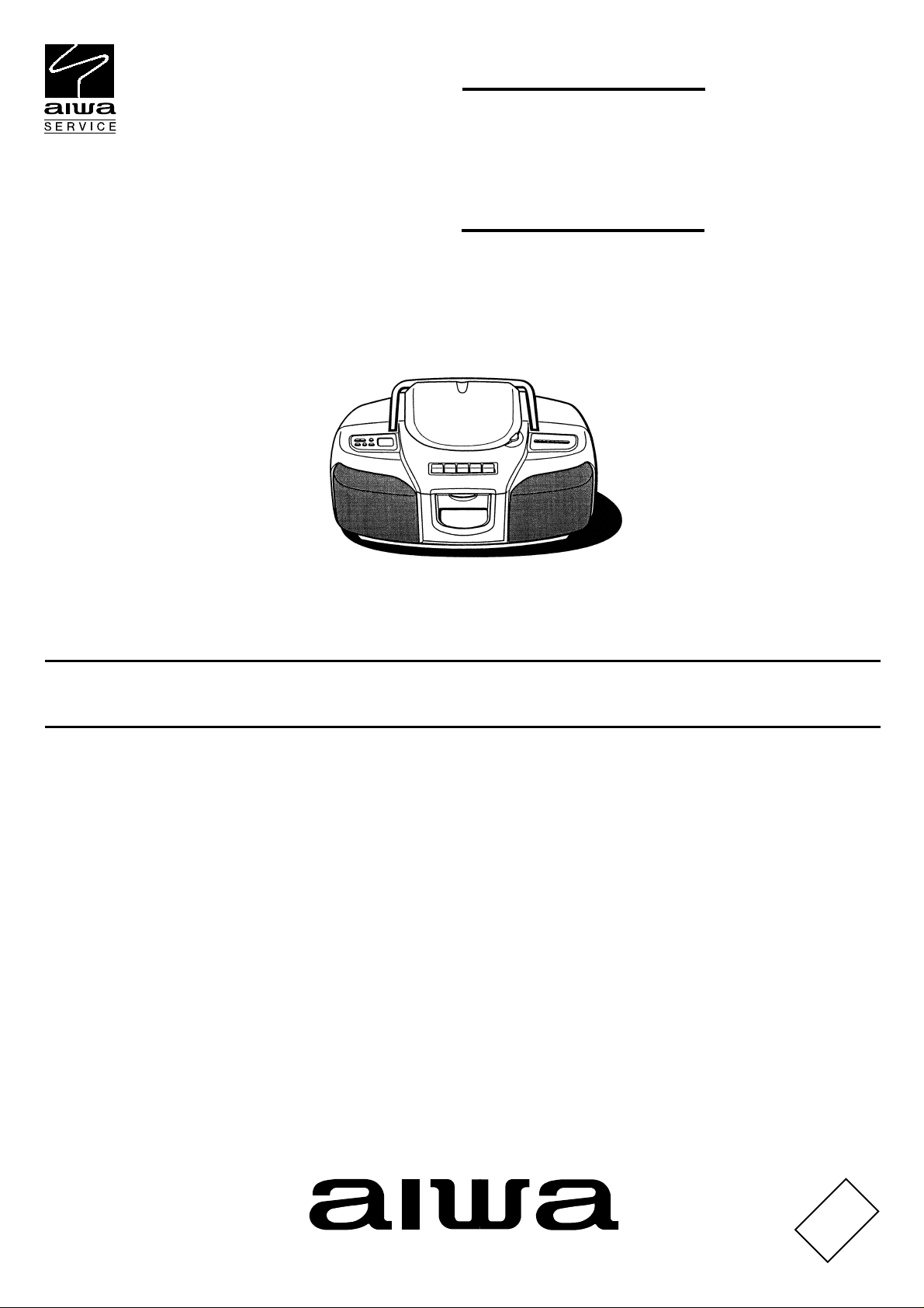
CSD-A120
U(S),K(S)
HS(S),HRJ(S)
EZ(S),LH(S)
HRJ(L),HRJ(P)
CSD-A140
LH(S)
SERVICE MANUAL
COMPACT DISC STEREO
CASSETTE RECEIVER
BASIC TAPE MECHANISM : TN-9ZR-219
BASIC CD MECHANISM : DA11T3C
S/M Code No. 09-014-356-0N1
DATA
Page 2
120HR, K, E, HS MODEL
SPECIFICATIONS
120LH, 140LH MODEL
Design and specifications are subject to change without
•
notice
.
120U MODEL
Design and specifications are subject to change without
•
notice
.
-2-
Design and specifications are subject to change without
•
notice
.
Page 3
PROTECTION OF EYES FROM LASER BEAM DURING SERVICING
This set employs laser. Therefore, be sure to follow carefully the
instructions below when servicing.
WARNING!
WHEN SERVICING, DO NOT APPROACH THE LASER EXIT
WITH THE EYE TOO CLOSELY. IN CASE IT IS NECESSARY TO
CONFIRM LASER BEAM EMISSION. BE SURE TO OBSERVE
FROM A DISTANCE OF MORE THAN 30cm FROM THE
SURFACE OF THE OBJECTIVE LENS ON THE OPTICAL
PICK-UP BLOCK.
Caution: Invisible laser radiation when
open and interlocks defeated avoid exposure to beam.
Advarsel:Usynling laserståling ved åbning,
når sikkerhedsafbrydere er ude af funktion.
Undgå udsættelse for stråling.
VAROITUS!
Laiteen Käyttäminen muulla kuin tässä käyttöohjeessa mainitulla tavalla saattaa altistaa käyt-täjän turvallisuusluokan 1 ylittävälle näkymättömälle lasersäteilylle.
VARNING!
Om apparaten används på annat sätt än vad som specificeras i
denna bruksanvising, kan användaren utsättas för osynling
laserstrålning, som överskrider gränsen för laserklass 1.
CAUTION
Use of controls or adjustments or performance of procedures
other than those specified herein may result in hazardous
radiation exposure.
ATTENTION
L'utilisation de commandes, réglages ou procédures autres que
ceux spécifiés peut entraîner une dangereuse exposition aux
radiations.
ADVARSEL!
Usynlig laserståling ved åbning, når sikkerhedsafbrydereer ude
af funktion. Undgå udsættelse for stråling.
This Compact Disc player is classified as a CLASS 1 LASER
product.
The CLASS 1 LASER PRODUCT label is located on the rear
exterior.
CLASS 1
KLASSE 1
LUOKAN 1
KLASS 1
LASER PRODUCT
LASER PRODUKT
LASER LAITE
LASER APPARAT
-3-
Page 4
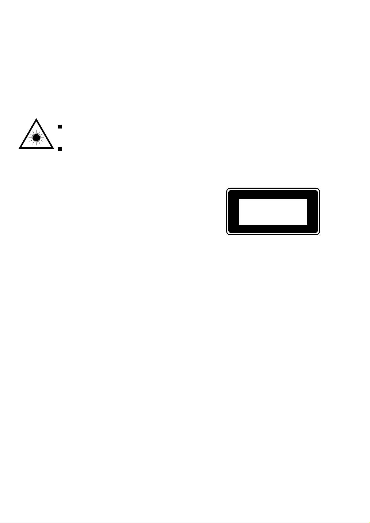
Precaution to replace Optical block
(SF-P101NR)
Body or clothes electrostatic potential could ruin
laser diode in the optical block. Be sure ground
body and workbench, and use care the clothes
do not touch the diode.
1) After the connection, remove solder shown in
the right figure.
PICK UP ASSY
SF-P101NR
Solder
1
16
TO/FROM MAIN C.B
-4-
Page 5

ELECTRICAL MAIN PARTS LIST-1/3
REF. NO PART NO. KANRI DESCRIPTION
NO.
IC
87-A21-271-010 IC,TA2111N<USC>
87-A20-212-010 IC,TA8127N<EXCEPT USC>
87-A20-569-010 IC,BA3308
8B-CDC-618-010 C-IC,LA9250ML
8B-CDC-619-010 C-IC,LC78602E
8B-CDC-636-010 C-IC,MM1469XH
8B-CDC-621-010 IC,UTC6650
87-A21-193-010 IC,TA8227P
87-A21-241-010 IC,MC14551BCP<140LHSC>
TRANSISTOR
8B-CDC-616-010 TR,3CG9012
8B-CDC-611-010 TR,2SD1936
8B-CDC-617-010 TR,3DG9013
89-318-155-080 TR,2SC1815GR
8A-RU2-602-010 TR,3DA8050
87-A30-015-080 TR,2SA1317(T/U)
87-026-215-080 TR,DTC114YS
8B-CDC-613-010 TR,2SA1346
8B-CDC-614-010 TR,2SB764
8A-RU2-604-010 TR,3CA8550
8B-RD3-607-010 TR,2SB562B
87-A30-090-080 FET,2SK2541
87-A30-168-010 TR,2SB1566F
DIODE
87-070-345-080 DIODE,IN4148
8Z-CA3-615-010 DIODE,1S2638<EXCEPT USC>
8B-CDC-631-010 ZENER,BZX55C6V8CECCL
8B-CDC-622-010 DIODE,GMB01
87-020-465-080 DIODE,1SS133(T-72)<USC>
8B-CDC-630-010 ZENER,WZ-033
87-A40-398-010 DIODE,1N4001
MAIN C.B
C101 87-A11-875-010 CAP,CER 24P-50 J SL<USC>
C101 87-A11-849-080 CAP,CER 27P-50 J CH<EXCEPT USC>
C103 87-A11-875-010 CAP,CER 24P-50 J SL
C104 88-254-242-010 CAP,CER 30P-50 J CH HE50S JCH
C105 87-A10-577-010 CAP,CER 0.022-50 Z YF
C106 87-A10-139-010 CAP,CER 18P-50 K CH<EXCEPT USC>
C106 88-RU7-634-010 CAP,CER 20P-50 J CH<USC>
C107 87-A10-577-010 CAP,CER 0.022-50 Z YF<USC>
C108 88-RU7-634-010 CAP,CER 20P-50 J CH
<EXCEPT 120LHSC,140LHSC>
C108 87-A11-847-080 CAP,CER 22P-50 J CH<140LHSC>
C108 87-A11-848-080 CAP,CER 24P-50 J CH<120LHSC>
C109 87-A10-129-010 CAP,CER 3P-50 K CH
C110 87-A10-577-010 CAP,CER 0.022-50 Z YF<120LHSC,140LHSC>
C113 87-010-265-080 CAP, ELECT 33-16V
C114 87-010-400-010 CAP, ELECT 0.47-50SME<EXCEPT USC>
C115 87-010-400-010 CAP, ELECT 0.47-50SME
C116 87-A10-176-010 CAP,CER 1000P-50 M D<EXCEPT USC>
C116 87-A11-146-080 CAP,TC U 0.022-50 Z F<USC>
C117 87-010-401-080 CAP, ELECT 1-50V<EXCEPT USC>
C118 87-010-401-080 CAP, ELECT 1-50V<USC>
C118 87-010-403-080 CAP, ELECT 3.3-50V<EXCEPT USC>
C119 87-010-400-010 CAP, ELECT 0.47-50SME<USC>
C119 87-010-401-080 CAP, ELECT 1-50V<EXCEPT USC>
C120 87-A10-176-010 CAP,CER 1000P-50 M D
C121 87-A10-577-010 CAP,CER 0.022-50 Z YF<EXCEPT USC>
C122 87-A10-577-010 CAP,CER 0.022-50 Z YF<EXCEPT USC>
C123 87-A12-366-080 CAP,M 0.015-100 J CP
C124 87-A12-366-080 CAP,M 0.015-100 J CP
C125 87-010-545-080 CAP, ELECT 0.22-50V
C126 87-010-545-080 CAP, ELECT 0.22-50V<USC,140LHSC>
REF. NO PART NO. KANRI DESCRIPTION
C127 87-A12-365-080 CAP,M 0.012-100 J CP<EXCEPT KSC,EZSC>
C127 87-A12-362-080 CAP,M 6800P-100 J CP<KSC,EZSC>
C128 87-A12-365-080 CAP,M 0.012-100 J CP
C128 87-A12-362-080 CAP,M 6800P-100 J CP<KSC,EZSC>
C129 87-A10-577-010 CAP,CER 0.022-50 Z YF
C130 87-A10-577-010 CAP,CER 0.022-50 Z YF<EXCEPT USC>
C140 87-A11-145-080 CAP,TC U 0.01-50 Z F<EXCEPT 140LHSC>
C141 87-A11-148-080 CAP,TC U 0.1-50 Z F<EXCEPT USC,140LHSC>
C142 87-A11-145-080 CAP,TC U 0.01-50 Z F<EXCEPT 140LHSC>
C143 87-A10-176-010 CAP,CER 1000P-50 M D<USC>
C144 87-A11-145-080 CAP,TC U 0.01-50 Z F<USC>
C145 87-A11-145-080 CAP,TC U 0.01-50 Z F<USC>
C152 87-A11-145-080 CAP,TC U 0.01-50 Z F<USC>
C155 87-A10-176-010 CAP,CER 1000P-50 M D
C180 87-010-248-010 CAP, ELECT 220-10V
C313 87-010-401-080 CAP, ELECT 1-50V
C314 87-010-401-080 CAP, ELECT 1-50V
C361 87-010-248-010 CAP, ELECT 220-10V
C362 87-010-263-080 CAP, ELECT 100-10V
C401 87-010-405-080 CAP, ELECT 10-50V
C402 87-A10-182-010 CAP,CER 0.01-50 Z F
C403 87-010-248-080 CAP, ELECT 220-10V
C403 87-010-248-080 CAP, ELECT 220-10V
C404 87-010-260-080 CAP, ELECT 47-25V
C405 87-A10-182-010 CAP,CER 0.01-50 Z F
C406 87-010-263-080 CAP, ELECT 100-10V
C407 87-010-546-080 CAP, ELECT 0.33-50V
C408 87-A10-182-010 CAP,CER 0.01-50 Z F
C409 87-010-263-080 CAP, ELECT 100-10V
C410 87-A12-370-080 CAP,M 0.033-100 J CP
C411 87-010-405-080 CAP, ELECT 10-50V
C413 87-010-263-080 CAP, ELECT 100-10V
C414 87-010-402-080 CAP, ELECT 2.2-50V
C415 87-A12-370-080 CAP,M 0.033-100 J CP
C419 87-A10-182-010 CAP,CER 0.01-50 Z F
C420 87-010-402-080 CAP, ELECT 2.2-50V
C424 87-A12-370-080 CAP,M 0.033-100 J CP
C426 87-010-544-080 CAP, ELECT 0.1-50V
C427 87-A10-179-010 CAP,CER 3300P-50 M E
C428 87-A12-371-080 CAP,M 0.039-100 J CP
C429 87-A11-782-080 CAP,M 0.1-100 J
C430 87-A11-782-080 CAP,M 0.1-100 J
C431 87-A10-176-010 CAP,CER 1000P-50 M D
C432 87-A11-782-080 CAP,M 0.1-100 J
C433 87-A12-370-080 CAP,M 0.033-100 J CP
C434 87-A10-179-010 CAP,CER 3300P-50 M E
C436 87-010-545-080 CAP, ELECT 0.22-50V
C437 87-010-401-080 CAP, ELECT 1-50V
C438 87-A10-179-010 CAP,CER 3300P-50 M E
C439 87-010-260-080 CAP, ELECT 47-25V
C440 87-A11-782-080 CAP,M 0.1-100 J
C441 87-A10-577-010 CAP,CER 0.022-50 Z YF
C442 87-010-221-080 CAP, ELECT 470-10V
C443 87-A10-182-010 CAP,CER 0.01-50 Z F
C444 87-010-263-080 CAP, ELECT 100-10V
C445 87-A10-577-010 CAP,CER 0.022-50 Z YF
C448 87-010-544-080 CAP, ELECT 0.1-50V
C453 87-A10-577-010 CAP,CER 0.022-50 Z YF
C454 87-010-263-080 CAP, ELECT 100-10V
C456 87-010-370-040 CAP,E 330-6.3 SME
C457 87-010-221-080 CAP, ELECT 470-10V
C459 87-010-263-080 CAP, ELECT 100-10V
C460 87-010-236-080 CAP,E 1000-10 SME
C461 87-010-403-080 CAP, ELECT 3.3-50V
C462 87-010-403-080 CAP, ELECT 3.3-50V
C465 87-A10-210-010 CAP,CER 0.047-50 M
C466 87-A10-176-010 CAP,CER 1000P-50 M D
C467 87-A10-182-010 CAP,CER 0.01-50 Z F
NO.
<EXCEPT KSC,EZSC,140LHSC>
<EXCEPT USC,140LHSC>
-5-
Page 6

ELECTRICAL MAIN PARTS LIST-2/3
REF. NO PART NO. KANRI DESCRIPTION
NO.
C481 87-A11-145-080 CAP,TC U 0.01-50 Z F<USC>
C484 87-A10-176-010 CAP,CER 1000P-50 M D
<EXCEPT USC,EZSC,140LHSC>
C485 87-A11-145-080 CAP,TC U 0.01-50 Z F
<EXCEPT 120LHSC,USC,140LHSC>
C486 87-010-263-080 CAP, ELECT 100-10V<EXCEPT KSC,EZSC>
C487 87-A11-148-080 CAP,TC U 0.1-50 Z F
<HRJSC,HRJPC,HRJLC,KSC,HSSC>
C488 87-A11-145-080 CAP,TC U 0.01-50 Z F
<EXCEPT 120LHSC,140LHSC>
C502 87-010-248-080 CAP, ELECT 220-10V
C503 87-A10-176-010 CAP,CER 1000P-50 M D
C505 87-010-263-080 CAP, ELECT 100-10V
C801 87-A11-891-080 CAP,CER 470P-50 J SL
C802 87-A11-891-080 CAP,CER 470P-50 J SL
C805 87-010-545-080 CAP, ELECT 0.22-50V
C806 87-010-545-080 CAP, ELECT 0.22-50V
C807 87-A10-176-010 CAP,CER 1000P-50 M D
C808 87-A10-176-010 CAP,CER 1000P-50 M D
C809 87-010-405-080 CAP, ELECT 10-50V
C810 87-010-405-080 CAP, ELECT 10-50V
C811 87-010-263-080 CAP, ELECT 100-10V
C812 87-010-263-080 CAP, ELECT 100-10V
C813 87-010-386-080 CAP,E 330-25 M SME
C814 87-010-386-080 CAP,E 330-25 M SME
C817 87-A12-380-080 CAP,M 0.22-100 J CP
C818 87-A12-380-080 CAP,M 0.22-100 J CP
C819 87-010-101-080 CAP, ELECT 220-16
C820 87-010-386-080 CAP,E 330-25 M SME
C821 87-010-401-080 CAP, ELECT 1-50V
C856 87-010-405-080 CAP, ELECT 10-50V
C857 87-010-237-080 CAP,E 1000-16 M SME
C858 87-010-388-080 CAP,E 1000-25 M SME
CF101 87-008-582-010 FLTR,SFU455B
CF102 87-008-261-010 FILTER, SFE10.7MA5-A<EXCEPT USC>
CF102 87-008-582-010 FLTR,SFU455B<USC>
CF103 87-A90-420-010 FLTR,CF CDA10.7MG1<USC>
CN310 8B-CDC-677-010 F-CABLE ASSY,7P 2 93MM
CN401 8B-CDC-660-010 CONN,16P V TOC-B
CN402 8B-CDC-661-010 CONN ASSY,6P CD-ME
CN403 8B-CDC-663-010 F-CABLE ASSY,5P 2 153MM
CN404 8B-CDC-664-010 F-CABLE ASSY,8P 2 153MM
CN801 8B-CDC-657-010 CONN,4P V SPK-0UT
CN851 8B-CDC-658-010 CONN,3P V BATT
CNH401 8B-CDC-665-010 FF-CABLE,16P 1 200MM
HP801 8B-CDC-629-010 JACK,HTJ035-08D
L101 8B-CDC-640-010 COIL,FMRF4T5MM
L102 8B-CDC-639-010 COIL,FMOSC3T5MM
L103 8B-CDC-640-010 COIL,FMRF4T5MM
L104 8B-CDC-673-010 COIL,AM IFT
L105 87-005-849-080 COIL,10UH(CECS)<EXCEPT USC>
L402 87-005-684-080 COIL,10UH J LF0.5S
L803 87-005-680-080 COIL,4.7UH J LF5.0S<EXCEPT 140LHSC>
LF401 87-A90-133-010 SW LEAF LSA1120JAU
R475 87-029-366-090 FUSING RESISTOR, 1/2W-4.7 F
SW101 8B-CDC-644-010 SW,SL 2-2-2 SK22F03G9AA
SW102 8B-CDC-644-010 SW,SL 2-2-2 SK22F03G9AA
SW801 8B-CDC-643-010 SW,SL 2-4-3 SK43D01G9AA
T101 8B-CDC-672-010 COIL,AM OSC
T102 8B-CDC-674-010 COIL,FM IFT1<EXCEPT USC>
T103 8B-CDC-673-010 COIL,AM IFT<EXCEPT USC>
T103 8B-CDC-688-010 IFT, 4A-224R<USC>
T105 8B-CDC-675-010 COIL,FM DET<EXCEPT USC>
VC101 8B-CDC-671-010 TUN-CAP,20P-126P DF443DF02-A04
VR101 8B-CDC-634-010 SFR,10K<EXCEPT USC>
VR501 8B-CDC-633-010 SFR,500 H
VR801 8A-RU2-661-010 VR,50KC
WH401 8B-CDC-662-010 F-CABLE ASSY,2P 2 253MM
X401 8Z-CD5-633-010 VIB, CER16.93MHZ FCR16.93M2
REF. NO PART NO. KANRI DESCRIPTION
RECTIFIER C.B
C851 87-A10-182-010 CAP,CER 0.01-50 Z F
C852 87-A10-182-010 CAP,CER 0.01-50 Z F
C853 87-A10-182-010 CAP,CER 0.01-50 Z F
C854 87-A10-182-010 CAP,CER 0.01-50 Z F
C855 87-010-388-080 CAP,E1000-25 M SME
CASETTE C.B
C216 87-010-248-080 CAP, ELECT 220-10V
C219 87-A10-176-010 CAP,CER 1000P-50 M D
C301 87-010-405-080 CAP, ELECT 10-50V
C302 87-010-405-080 CAP, ELECT 10-50V
C303 87-A10-179-010 CAP,CER 3300P-50 M E
C304 87-A10-179-010 CAP,CER 3300P-50 M E
C305 87-010-382-080 CAP,E 22-25 M 11L SME
C306 87-010-382-080 CAP,E 22-25 M 11L SME
C307 87-A12-369-080 CAP,M 0.027-100 J CP
C308 87-A12-369-080 CAP,M 0.027-100 J CP
C309 87-010-404-080 CAP, ELECT 4.7-50V
C310 87-010-404-080 CAP, ELECT 4.7-50V
C311 87-A12-356-080 CAP,M 2200P-100 J CP
C312 87-A12-356-080 CAP,M 2200P-100 J CP
C315 87-010-221-080 CAP, ELECT 470-10V
C316 87-010-405-080 CAP, ELECT 10-50V
C317 87-A10-182-010 CAP,CER 0.01-50 Z F
C318 87-A10-182-010 CAP,CER 0.01-50 Z F
C323 87-A10-182-010 CAP,CER 0.01-50 Z F
C351 87-A11-112-080 CAP,TC U 1000P-50 J CH<140LHSC>
C352 87-A10-182-010 CAP,CER 0.01-50 Z F
C353 87-A10-182-010 CAP,CER 0.01-50 Z F
CN301 8B-CDC-659-010 CONN,4P V T-HEAD
SW301 8B-CDC-635-010 SW,SL 1-9-2 PS92D01
T351 87-CD8-605-010 COIL,OSC BIAS 4A363R
VR351 8B-CDC-634-010 SFR,10K
CD KEY&DISPLAY C.B
DP401 8B-CDC-624-010 LED,A505RDD
LED401 87-070-106-010 LED,SE3001DT R
SW401 8B-CDC-623-010 SW,TACT 1102B160G
SW402 8B-CDC-623-010 SW,TACT 1102B160G
SW403 8B-CDC-623-010 SW,TACT 1102B160G
SW404 8B-CDC-623-010 SW,TACT 1102B160G
SW405 8B-CDC-623-010 SW,TACT 1102B160G
SW406 8B-CDC-623-010 SW,TACT 1102B160G
BATTERY C.B
SENSOR C.B<140LHSC>
C201 87-010-378-080 CAP,E 10-16M 11L SME<140LHSC>
CN201 8B-CDN-601-010 CONN,3P REMOTE<140LHSC>
MOTOR C.B
M2 S0-M10-A09-700 MOTOR SLED ASSY
PIN3 S2-369-750-000 PLUG,6P
SW1 S4-S13-A01-600 SW,LEAF
NO.
-6-
Page 7
ELECTRICAL MAIN PARTS LIST-3/3
• Regarding connectors, they are not stocked as they are not the initial order items.
The connectors are available after they are supplied from connector manufacturers upon the order is received.
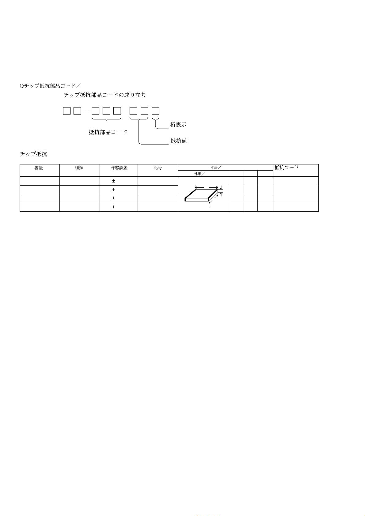
CHIP RESISTOR PART CODE
Chip Resistor Part Coding
88
A
Resistor Code
Chip resistor
Wattage Type Tolerance
1/16W 1005 5% CJ
1/16W
1/10W
1/8W
1608
2125
3216
5%
5%
5%
Symbol
CJ
CJ
CJ
Figure
Value of resistor
Form
L
Dimensions (mm)
t
W
0.55
Resistor Code
108
118
128
LW t
1.0 0.5 0.35 104
1.6 0.8 0.45
2 1.25 0.45
3.2
1.6
: A
: A
-7-
Page 8
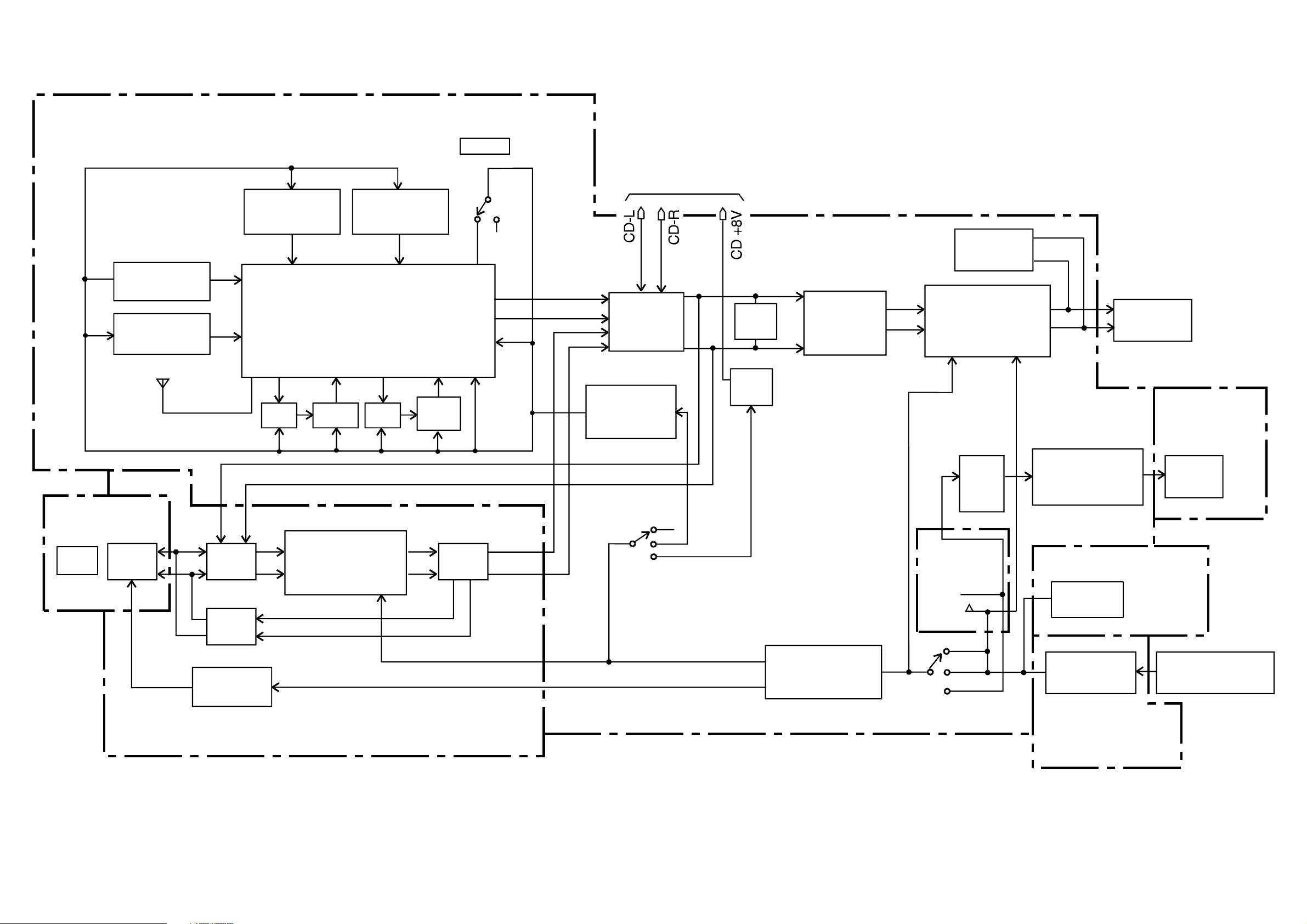
BLOCK DIAGRAM-1/2 (TUNER, CASETTE&POWER AMP)
MAIN C.B (1/2)
AMRF
L104,VC101B
FM RF
L103,VC101D
FM
ANT
MECHANISM
TN-9ZR-219 (1/3)
R/EHP
HEAD
T351,Q352
T101,VC101A
24
23
1
SW301
A.G
SW301
B.C
AC BIAS
AM OSC
20
MIX. IF AMP & DET
3
T102
2
IC301,BA3308
8
FM OS
L102, VC101C
21
IC101TA8127
8
CF102
PRE AMP
4
T103
6
VCC
3
7
C
7
CF101
455K
SW301
SW101
BAND
AM
16
13
14
22
6
D.E
FM
R-CH
L-CH
R-CH
L-CH
TO MAIN C.B (2/2)
SW802
B,D
REGULATOR
Q161,Q163
TAPE
SW801C
CD
RADIO
Q801
Q802
Q851
Q852
VOLUME
VR801
A,B
REGULA TOR
Q362,Q361,D363
PHONES
6
POWER AMP
IC801,TA8227
7
1
VCC2
Q502
Q501
D503
MECHANISM
TN-9ZR-219
(3/3)
SW501
LEAFSW
TAPE
RADIO
CD
SW801A
HP801
2
11
12
VCC1
MOTOR
3
REGULATOR
IC501,UT6650
BATTERY C.B
DC 12V
RECTIFIER
D851~D854
SPEAKER
MECHANISM
TN-9ZR-219 (2/3)
M501
2222
DECK
MOTOR
TRANSFORMER
CASETTE C.B
RECTIFIER
C.B
-8-
Page 9
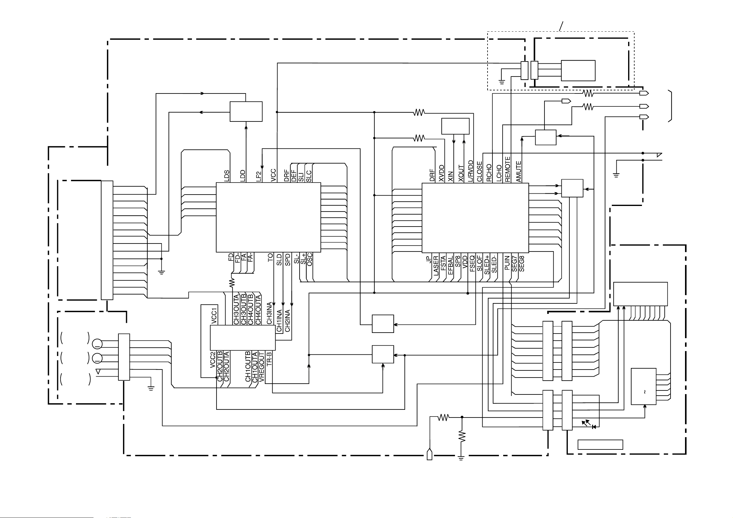
BLOCK DIAGRAM-2/2 (CD)
140LH
CD MECHANISM
DA11T3C
CN401
OPTIGAL
PICK UP
SF-P101NR
MAIN C.B (2/2)
VREF
1
COM
2
E
3
D
4
A
5
B
6
C
7
F
8
GND
9
LD
10
VR
11
MO
12
F+
13
T-
14
T+
15
F-
16
FIN2
FIN1
E
F
1
2
3
4
Q401
63
62
LA9250M
1718191520
59
ASP
IC401
56
525150
2826293031
LF2
45
49
44
43
42
41
40
38
37
36
35
33
CLV
HFL
TES
TOFF
TGL
TJP
LASER
FSTA
EFBAL
SP8
SLOF
DEF
VVDD
FR
VSS
EFMO
EFMIN
CLV
HFL
TES
TOFF
TGL
X40
1
16.934M
64
62
61
1
6
7
8
9
10
12
13
14
15
171819202122232526
16
60
DSP
IC402
LC78602E
55
58
575452
REM401
27
283231
SENSOR C.B
SENSOR
CN201
MUTE
Q407
42
51
41
44
38
37
36
35
34
33
43
DIG1
DIG2
KEYIN
SEG1
SEG2
SEG3
SEG4
SEG5
SEG6
PROG
Q405
Q406
RCH
LCH
+8V
LF401
LFSW
CD KEY &
DISPLAY C.B
LED DISPLAY
DP401
TO MAIN C.B (1/2)
MOTOR C.B
M3
SPINDLE
MOTOR
M2
SLED
MOTOR
SW1
INSIDE
LIMIT SW
M
M
CN402
SPIN+
1
SPIN-
2
SM+
3
SM-
4
PU-IN-SW
5
GND
6
CH4INA
BIAS IN
23
25
21
IC403
MM1469XH
22
11
12
17
18
216
26
27
3
10
19
5
IC403
DRIVER
+5V
-9-
Q403
Q404
+8V
+8V
TO MAIN C.B
(1/2)
CN404
DISP08
DISP07
DISP06
DISP05
DISP04
DISP03
DISP02
DISP01
CN403
KEYIN
DIG1
DIG2
PROG
8
7
6
5
4
3
2
1
1
2
3
4
5
CN4404
8
7
6
5
4
3
2
1
CN4403
1
2
3
4
5
KEY
MATRIX
SW401
SW406
LED401
PROGRAM
Page 10
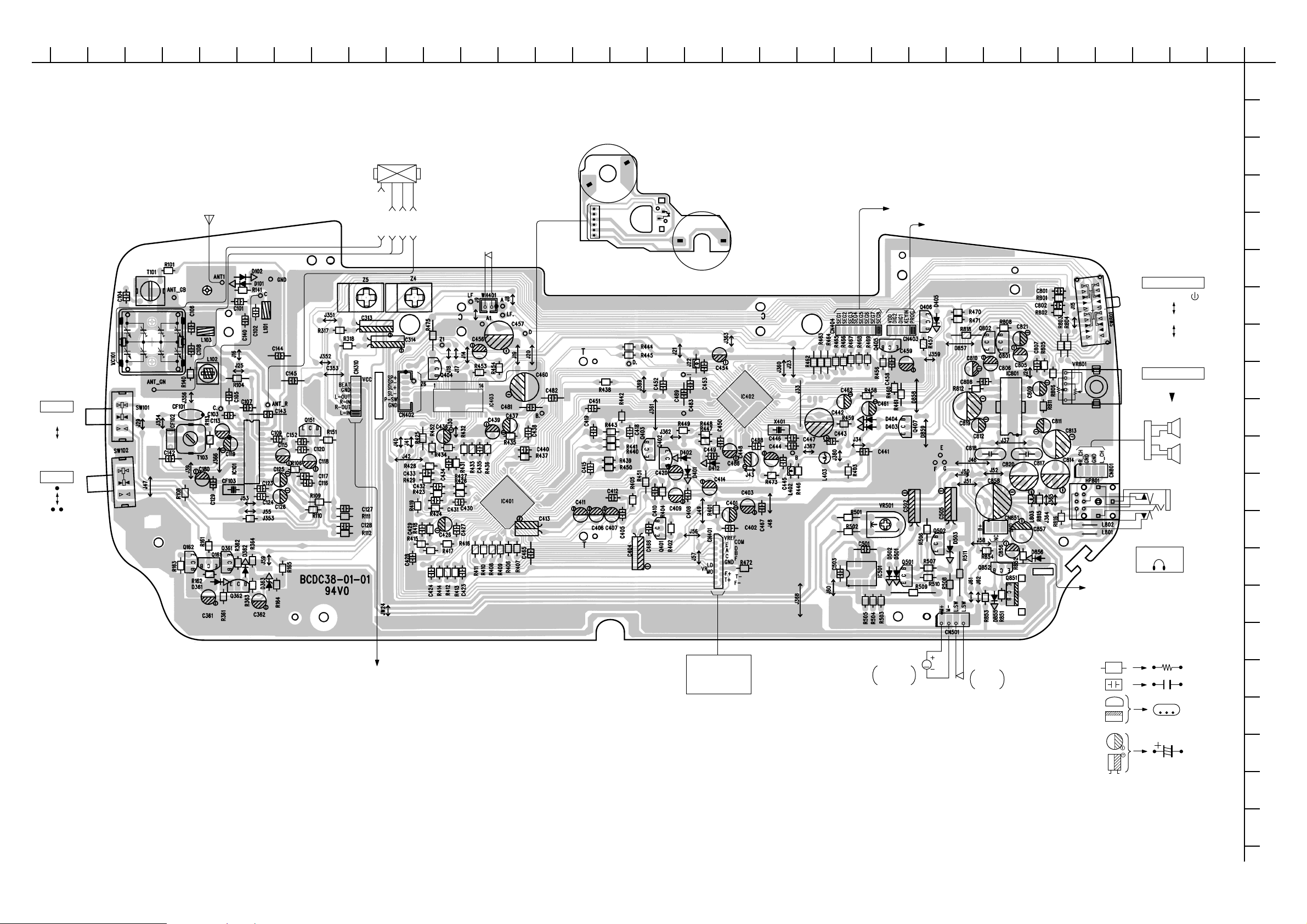
WIRING-1/4 (MAIN/U MODEL, MOTOR)
MAIN C.B
(INSERTED PARTS)
FM ANT.
L104
MW COIL
GRN
VIO
NATURAL
RED
LF401
LF SW
MOTOR C.B
(CONDUCTOR SIDE)
M2
+
_
6
PIN3
1
M2
(SLED MOTOR)
SW1
(INSIDE LIMIT SW)
SW1
(SPINDLE MOTOR)
_
M3
101112131415161718192021222324
1234567892526272829303132
A
B
C
D
TO CD KEY&DISPLAY C.B CN4404
+
TO CD KEY&DISPLAY C.B CN4403
E
SW101
BAND
AM
FM
SW102
OSC
M3
SW801
F
FUNCTION
TAPE
STANDBY
G
RADIO
A
B
D
C
1
5
1
24
13
12
1
6
778
15212228
32 33
17
16
48
49
1
64
32 33
17
16
1
1
2
16
15
48
49
64
85
1
11
CD
H
VR801
6
7
4
9
VOLUME
MAX
I
MIN
3
10
12
1
4
1
1
2
3
4
CNH801
SPK1
2W
(LCH)
SPK2
2W
(RCH)
J
K
L
3
1
M
HP801
PHONES
N
4
1
4
TO RECTIFIER C.B
CNH851
O
TO CASETTE C.B
CN302
-10-
OPTICAL
PICK UP
SF-P101NR
M501
DECK
MOTOR
M
SW501
LEAF
SW
TATE MECHANISM
TN-9ZR-219 (2/2)
NOTE
Rxx
E C B
E C B
P
Q
E C B
R
S
T
U
Page 11
WIRING-2/4 (MAIN/EXCEPT U MODEL, MOTOR)
MAIN C.B
(INSERTED PARTS)
FM ANT.
L104
MW COIL
GRN
VIO
NATURAL
RED
LF401
LF SW
MOTOR C.B
(CONDUCTOR SIDE)
M2
+
_
6
PIN3
1
M2
(SLED MOTOR)
SW1
(INSIDE LIMIT SW)
SW1
(SPINDLE MOTOR)
_
M3
101112131415161718192021222324
1234567892526272829303132
A
140LH
SENSOR C.B
B
(INSERTED PARTS)
C
1
D
TO CD KEY&DISPLAY C.B CN4404
TO CD KEY&DISPLAY C.B CN4403
+
E
F
SW101
BAND
AM
FM
SW102
OSC
M3
except
EZ,K
except
A
B
D
C
140LH
140LH
except
140LH
except
1
5
1
12
LH
except
140LH
24
13
except
140LH
1
6
778
15212228
32 33
17
16
1
64
LH
except
140LH
48
49
16
17
16
except
LH,EZ
2
1
15
32 33
1
except
EZ,K
except LH
64
except LH
48
49
140LH
1
58
1
4
6
7
4
9
3
10
1
12
4
1
3
TO RECTIFIER C.B
SW801
FUNCTION
TAPE
RADIO
CD
VR801
VOLUME
MAX
MIN
1
2
3
4
CNH801
HP801
PHONES
STANDBY
SPK1
2W
(LCH)
SPK2
2W
(RCH)
G
H
I
J
K
L
M
N
O
CNH851
TO CASETTE C.B
CN302
-11-
OPTICAL
PICK UP
SF-P101NR
M501
DECK
MOTOR
1
4
M
SW501
LEAF
SW
TATE MECHANISM
TN-9ZR-219 (2/2)
NOTE
Rxx
E C B
E C B
P
Q
R
E C B
S
T
U
Page 12

WIRING-3/4 (CASETTE, CD KEY&DISPLAY)
101112131415161718192021222324
1234567892526272829303132
CASETTE C. B
(R/PH)
1234
CNH301
14
E CGH F A DB
EHL CH R CH
ME CHANISM
TN-9ZR-219 (1/2)
19
A
B
C
D
E
F
1
7
CN310
TO MAIN C. B
G
H
I
DP401
CD TRACK
CD KEY&DISPLAY C. B
SW401 SW406 SW402
PROGRAM
NOTE
Rxx
J
K
L
M
N
O
P
Q
R
LED401
PROGRAM
11
TO MAIN C. B
CN404
TO MAIN C. B
CN403
-12-
SW405 SW404 SW403
REPEAT
E C B
E C B
S
E C B
T
U
Page 13

WIRING-4/4 (RECTIFIER, BATTERY)
123456789101112131415
BATTERY C. B
(INSERTED PARTS)
RECTIFIER C. B
(INSERTED PARTS)
DRT BATTERY
R20 X 8
DC 12V
A
B
C
D
E
F
G
H
I
U,EZ,K,HS
MODEL
LH,HRJ
MODEL
TU (U,EZ,K,HS)
TU
SW901
CNH851
AC
U : 120V 60Hz
HS : 220V 60Hz
EZ, K : 230V 50Hz
AC
110 - 120V
220 - 240V
50/60Hz
J
K
L
M
3
1
CN851
TO MAIN C. B
N
O
P
Q
NOTE
Rxx
R
S
E C B
E C B
E C B
T
SW901
VOLT AGE
SELECT
220 - 240V
110 - 120V
-13-
U
Page 14

SCHEMATIC DIAGRAM-1/3 (TUNER U MODEL)
MAIN C.B (1/2)
T101,VC101A
AM FREQ. ADJ.
AM OSC
0.001 0.002
L104,VC101B
AM TRACKING ADJ.
0.01
0.01
50V
C322
100P
R
P
R
P
P
R
R
L103,VC101D
FM TRACKING ADJ.
FM RF
0.01
25V
47uF
0.027
6.8K
2200P
2200P
50V
4.7K
P
AM IFT
L102,VC101C
FM FREG. ADJ.
T103
AM IFT ADJ.
50V
4.7K
R
0.01
0.01
6.8K
MIX IF & DET
PRE AMP
R
4.7K
FM OSC
33uF
16V
P
SW301A-H
(REC/PB SW)
47uF
50V
P
R
C107
0.022
0.027
4.7K
25V
6.8K
1000P
P
0.47uF
50V
0.01
50V
FM SW
0.01
3300P
0.01
R
50V
0.022
3.3K
10V
50V
0.022
0.1
1.5K
1.5K
BAND
0.0150.015
CN302
CN310
F-CABLE
50V
50V
5.6K
OSC
5.6K
0.012
8.2K
0.012
REG
REG
STANDBY
50V
FUNCTION
FUNCTION
FUNCTION
STANDBY
50V
STANDBY
6.8K
3.3K
3.3K
50V
VOLUME
VOLUME
WZ-033
4.7K
MUTE
MUTE
50V
50V
REG
50V
1000P
1000P
REG
REG
REG
10uF 50V
10uF 50V
TO MAIN C.B (2/2)
POWER
AMP
MOTOR
REG
1000P
0.022
100V
0.1
0.022
100V
9.1K
VR501
NORMAL TAPE
SPEED ADJ.
JW
JW
PHONES
(LCH)
(RCH)
MECHANISM
TN-9ZR-219(2/2)
L
MECHANISM
TN-9ZR-219(1/2)
3.3K
0.047uF
100V
FREQ. ADJ.
T351
AC BIAS
0.01
BEAT
SW
CASETTE C.B
AC BIAS LEVEL
0.01
0.01
AC BIAS
R
P
ADJ.
10V
REG
1.8K
10V
REG
FUNCTION
SIGNAL :
STANDBY
: PB/FM
RECTIFIER C.B
BATTERY C.B
R20X8
DC 12V
TU
D857
1N4001
AC 120V,60Hz
AC~
: REC/AM
-14-
Page 15

SCHEMATIC DIAGRAM-2/3 (TUNER EXCEPT U MODEL)
X : NO MOUNT
Ref. No.
HRJ
50V
STANDBY
25V
C108
C110
C127,128
C140
C141
C155
C351
R109,110
R111,112
R140
R141
L803
20P
X
0.012 0.0126800P
50V
6.8K
3.3K
VOLUME
VOLUME
50V
3.3K
WZ-033
MAIN C.B (1/2)
T101,VC101A
AM FREG. RANGE ADJ.
L103,VC101D
FM FREQ.TRACKING ADJ.
VC101
TUNING
L104,VC101B
AM TRACKING ADJ.
50V
C322
100P
R
C
P
R
P
P
R
R
25V
0.027
6.8K
2200P
2200P
4.7uF
50V
P
4.7K
AM OSC
0.022
0.022
R
0.01
0.01
50V
4.7K
AM IFT
FM IF ADJ.
PRE AMP
P
R
4.7K
(REC/PB SW)
L102,VC101C
FM FREG. RANGE ADJ.
R140
C142
0.01
4.7uF
50V
0.027
4.7K
P
R
SW301A-H
6.8K
25V
VR101
VCO FREQ.ADJ.
BAND
OSC
REG
REG
0.022
STANDBY
STANDBY
50V
FUNCTION
SW801
SW801
FUNCTION
FUNCTION
3.3uF
1000P
50V50V
50V
50V
30P
15
AM IF ADJ.
0.01
50V
3300P
C
R
P
16V
1000P
50V
MIX IF & DET
1.5K
1.5K
50V
0.015
77
1
CN302
4.7K
1
F-CABLE
0.015
FM DET
CN310
C351
50V
FM IF ADJ.
0.022
0.022
120 LH
24P
0.022
0.01
0.1
1000P
X
2.7K
X
4.7µH
K
10V
EZ HS
20P
X
X
4.7K
MUTE
MUTE
50V
140 LH
22P
0.022
X
X
X
1000P
X
8.2K8.2K 15K
33K
1K1K
Jamper
REG
REG
1000P
1000P 10uF 50V
REG
REG
50V
50V
10uF 50V
TO MAIN C.B (2/2)
123 4
876 5
POWER
AMP
MOTOR
REGULATOR
0.022
100V
0.022
100V
1000P
10V
10V
9.1K
0.1
VR501
NORMAL TAPE
SPEED ADJ.
L803
PHONES
MECHANISM
TN-9ZR-219(2/2)
(LCH)
(RCH)
DECK
L
MECHANISM
TN-9ZR-219(1/2)
3.3K
0.047uF
50V
T351
AC BIAS
FREQ. ADJ.
0.001
BEAT
SW
CASETTE C.B
AC BIAS LEVEL
0.01
0.01
AC
BIAS
R
P
ADJ.
10V
REG
1.8K
10V
REG
STANDBY
FUNCTION
SIGNAL :
: PB/FM
: REC/AM
BATTERY
C.B
R20X8
DC 12V
D857 1N4001
RECTIFIER C.B
VCD139ENFN
VBCD12DSFN
TU (EZ,K)
TU (HS)
THERMAL FUSE
EZ, K: 230V 50Hz
HS: 220V 60Hz
AC~
TU (LH,HRJ)
VBCD12DSFN
110V/220V SW
SW901
THERMAL FUSE
SW901
VOLTAGE
SELECT
110-120V
220-240V
50/60Hz
AC~
-15-
Page 16

SCHEMATIC DIAGRAM-3/3 (CD)
MAIN C.B (2/2)
OPTIGAL
PICK UP
SF-P101NR
50V
0.01
0.01
10V
25V
10V
LD CONT
0.033 100V
0.1
2.2K
0.1 100V
1000P
3300P
0.01
50V
50V
6.8K
10V
0.033
100V
50V
ASP
4.7K
2.2uF
50V
10V
0.01
REG
0.033
2.2uF
50V
C487
C484
U
D412
1SS133
0.1
0.1
U
10V
0.022
10V
R473
50V
1.2K
0.01
L402
10uH
C445
0.022
4.7K
C485
J34
100
1
1
2
2
3
3
CN201REM401
C488
0.01
EXCEPT LH
MUTE SW
3.3uF 50V
3.3uF 50V
SEN201
MC14551
BCP
C201
10uF
16V
2.2K
2.2K
X : NO MOUNT
Ref.No.
HRJ
R473
150
C486
C485
C484
C487
X
E 100/10V E 100/10V
0.01 0.01
0.001 0.001
0.1 0.1 0.1
SENSOR
C.B
K
EZ HS
U
220
150
X
X
X
X
140 LH
TO MAIN C.B (1/2)
140 LH120 LH
X
X
X
XX
WH401
CD
MECHANISM
DA11T3C
MOTOR
C.B
M3
SPINDLE
MOTOR
SLED
M2
MOTOR
INSIDE
SW1
LIMIT SW
10V
C489
5V REG
0.1
U
EQ SW
0.022
10V
10V
C483
0.1
EXCEPT
U,LH
U
TO MAIN C.B (1/2)
3.9K
3.9K
Q405,406
DRIVER
SW401
SW402
SW403
SW404
SW405
PROGRAM
LED401
LHU
A505
RDD
CD TRACK
SW406
REPEAT
PROGRAM
CD KEY &
C482 0.1
C482 0.1
DISPLAY
0.1 100V
0.1
100V
1000P
IC403
MOTOR COIL
DRIVER
PIN3
M
M
100V
8.2K
0.033
100V
1.5K
0.1
3300P
2.7K
5.6K
50V
50V
1.8K
10V
25V
3300P
IN4148
J363
2.2µH
0.1
C481
0.01
U
6.3V
C.B
-16-
SIGNAL :
: PB
Page 17

TRANSISTOR ILLUSTRATION-1/1
ECB ECB ECB
2SC1815
BCE
2SB1566
DTC114YS
2SD1936
ECB ECB
3CA8550
3CG9012
2SB764
2SA1317
2SA1346
3DA8050
3DG9013
SDG
2SK25412SB562
-17-
Page 18

IC BLOCK DIAGRAM-1/1
IC, BA3308
IC, MM1469XH
IC, TA8127N
28 27 26 25 24 23 22
10k
13k
Level shift
10k
T.S .D
10k
Level shift
13k
10k
1 2 3 4 5 6 7
Vcc
21 20 19 18 17 16 15
10k
Vcc
13k
Level shift
50k
DRIVER MUTE
50k
Level shift
13k
10k
8 9 10 11 12 13 14
IC, TA2111N
MPX IN
AGC
DET OUT
AF
BUFF
FM
MUTE
AM
DET
AM
IF
AM
IF INFMIF IN
AF
VCO
DIVIDE
LEVEL
FM
DET
DET
FM
IF
TUN
LEDSTLED
AM RF IN FM RF OUT FM OSC AM OSC AFC LPF2 LPF1 L-OUT R-OUTRF VCC
24 23 22 21 20 19 18 17 16 15 14
AM
FM
OSC
OSC
AM
MIX
FM
RF
FM RF IN RF GND MIX OUT AGC VCC GND TUN LED ST LED QUADAM
LOW CUT
FM
MIX
-18-
DECODE
ST/MO
FM/AM
1110987654321 12
13
Page 19

VOLTAGE CHART-1/2
THE MEASURED VALUE IS DC VOLTAGE
UNIT: V
TUNER SECTION
TEST CONDITION: SET AM/FM TUNER ON ONE FREQUENCY
IC101 (TA8127N)
PIN'S NUMBER 123456789101112
AM 0.74 0 3.19 3.19 0 3.19 3.19 3.19 0 0 2.77 3.20
FM 0 0 4.39 4.43 0.84 4.38 4.11 4.38 0 0 4.20 4.34
PIN'S NUMBER 13 14 15 16 17 18 19 20 21 22 23 24
AM 1.03 1.01 2.82 2.48 2.48 0.64 0.99 3.19 3.14 3.19 3.19 3.19
FM 1.05 1.03 3.77 4.22 3.87 0.70 1.37 4.34 4.41 4.41 4.41 4.41
TRANSISTOR Q161(9012) Q162(2SD1936)
EBCEBC
FM 7.03 6.34 6.95 0.33 0.88 6.34
CASSETTE & POWER SECTION
TEST CONDITION: TAPE PLAY
IC801 (TA8227P)
PIN'S NUMBER 123456789101112
PLAY 12.50 6.36 12.10 0 0.58 0 0 0.58 6.62 12.10 6.37 12.50
IC501 (UTC6650)
PIN'S NUMBER 12345678
2.03 3.31 3.37 3.17 0 0 1.45 0.69
IC301 (BA3308)
PIN'S NUMBER 123456789
1.84 0 1.85 0 0 6.71 1.88 0 1.85
TRANSISTOR Q352(8050C) Q362(2SD1936) Q361(9012)
EBCEBCEBC
TAPE PLAY 6.63 7.02 7.03 6.38 6.91 11.20 11.90 11.20 7.03
TAPE REC 0.06 7.00 0.65 6.36 6.91 10.80 11.50 10.90 7.00
TRANSISTOR Q501(9013G) Q502(2SB562)
EBCEBC
11.20 10.70 4.08 2.86 10.60 3.43
CD SECTION
TEST CONDITION: CD PLAY
IC402 (LC78602E)
PIN'S NUMBER 123456789101112
CD PLAY 0.02 0 1.60 0 1.59 4.93 0.36 0 2.46 2.40 0 2.60
PIN'S NUMBER 13 14 15 16 17 18 19 20 21 22 23 24
CD PLAY 0 1.56 0 4.93 2.50 4.90 0.43 0.43 0.03 4.93 4.93 0.03
PIN'S NUMBER 25 26 27 28 29 30 31 32 33 34 35 36
CD PLAY 0.03 0.05 0.06 4.90 2.50 1.78 2.93 2.93 4.88 2.93 2.93 0.95
PIN'S NUMBER 37 38 39 40 41 42 43 44 45 46 47 48
CD PLAY 3.00 0 0 2.80 2.75 4.91 4.91 0 0 0 0 0
PIN'S NUMBER 49 50 51 52 53 54 55 56 57 58 59 60
CD PLAY 0 0 4.93 2.00 0 1.74 4.20 0 1.76 0 0 1.80
PIN'S NUMBER 61 62 63 64
CD PLAY 2.00 4.92 4.92 4.85
-19-
Page 20

VOLTAGE CHART-2/2
IC401 (LA9250ML)
PIN'S NUMBER 123456789101112
CD PLAY 2.43 2.43 2.48 2.48 2.48 2.43 2.46 2.45 2.46 2.46 2.45 2.45
PIN'S NUMBER 13 14 15 16 17 18 19 20 21 22 23 24
CD PLAY 2.45 2.40 2.46 0 2.55 2.40 2.33 2.47 2.49 2.47 2.40 2.40
PIN'S NUMBER 25 26 27 28 29 30 31 32 33 34 35 36
CD PLAY 2.47 2.80 2.47 2.53 2.20 2.20 1.58 0.09 0 0.25 0.04 0.43
PIN'S NUMBER 37 38 39 40 41 42 43 44 45 46 47 48
CD PLAY 0.43 4.93 0.30 2.40 4.93 0.15 1.50 0 2.65 0 2.18 2.45
PIN'S NUMBER 49 50 51 52 53 54 55 56 57 58 59 60
CD PLAY 2.40 2.49 0 4.85 2.45 2.45 0 4.93 2.40 2.45 2.25 2.25
PIN'S NUMBER 61 62 63 64
CD PLAY 2.20 3.47 0.18 0.80
IC403 (MM1469XH)
PIN'S NUMBER 123456789101112
CD PLAY 2.89 2.95 2.53 2.48 5.33 5.08 4.73 0 2.48 2.78 3.36 2.56
PIN'S NUMBER 13 14 15 16 17 18 19 20 21 22 23 24
CD PLAY 0 6.06 0.81 0.83 2.93 3.00 2.48 2.46 6.56 6.56 2.47 2.47
PIN'S NUMBER 25 26 27 28
CD PLAY 2.49 2.96 2.93 0
TRANSISTOR Q404(2SB764) Q405(A8550) Q406(8550)
ECBECBECB
7.60 4.93 6.97 4.20 2.00 4.30 4.20 2.00 4.30
TRANSISTOR Q403(A1346) Q407(A1346)
ECBECB
4.90 2.20 4.90 4.90 4.90 0
-20-
Page 21

ELECTRICAL ADJUSTMENT-1/2 (U MODEL)
U MODEL
MAIN C.B
T101
2
L103
A
D
C
L102
IC101
T103
18
3
MW
COIL
L104
B
VC101
1
< TUNER SECTION >
1. AM IF Adjustment
Test point: IC101 (TA2111N) 18PIN
Adjustment location: T103
T103 ....................................................................... 455kHz
2. AM Frequency Range Adjustment
Test point: IC101 (TA2111N) 18PIN
Adjustment location: T101, VC101A
T101 ....................................................................... 517kHz
VC101A ............................................................... 1750kHz
3. AM Tracking Adjustment
Test point: IC101 (TA2111N) 18PIN
Adjustment location: L104, VC101B
L104 ............................................. 600kHz waveform max.
VC101B...................................... 1400kHz waveform max.
5
4
test
point
4. FM Frequency Range Adjustment
Test point: IC101 (TA2111N) 18PIN
Adjustment location: L102, VC101C
L102 ........................................................................87MHz
VC101C.................................................................109MHz
5. FM Tracking Adjustment
Test point: IC101 (TA2111N) 18PIN
Adjustment location: L103, VC101D
L103 ..............................................88MHz waveform max.
VC101D ......................................108MHz waveform max.
< DECK SECTION >
6. AC BIAS Frequency Adjustment
Test point: CN301 4PIN
Adjustment location: T351
T351 ................................................................ 60±0.5MHz
7. AC BIAS Level Adjustment
Test point: CN301 4PIN
Adjustment location: VR351
VR351 ................................................................... 14±0.5V
8. Normal Tape Speed Adjustment
Test point: HP801 (Headphone Jack)
Test Tape: B-111LNA
Adjustment location: VR501
VR501 .................................................................... 3000Hz
-21-
67
test point
6
7
T351
VR351
CASETTE C.B
CN301
4
MAIN C.B
HP801
VR501
8
Page 22

ELECTRICAL ADJUSTMENT-2/2 (EXCEPT U MODEL)
T351
VR351
CN301
4
67
6
7
test point
CASETTE C.B
8
VR501
HP801
MAIN C.B
EXCEPT U MODEL
MAIN C.B
T101
2
L104
MW
COIL
3
1
B
VC101
T102
T103
A
D
C
T105
L103
L102
11
IC101
19
VR101
4
< TUNER SECTION >
1. AM IF Adjustment
Test point: IC101 (TA8127N) 19PIN
Adjustment location: T103
(LH, HR, HS MODEL)
T103 ....................................................................... 455kHz
(EZ, K MODEL)
T103 ....................................................................... 465kHz
2. AM Frequency Range Adjustment
Test point: IC101 (TA8127N) 19PIN
Adjustment location: T101, VC101A
(LH MODEL)
T101 ....................................................................... 517kHz
VC101A ............................................................... 1750kHz
(HR, HS, K, EZ MODEL)
T101 ....................................................................... 513kHz
VC101A ............................................................... 1635kHz
3. AM Tracking Adjustment
Test point: IC101 (TA8127N) 19PIN
Adjustment location: L104, VC101B
L104 ............................................. 600kHz waveform max.
VC101B...................................... 1400kHz waveform max.
5. FM Frequency Range Adjustment
6. FM Tracking Adjustment
7. VCO Frequency Adjustment
6
5
7
~
6
7
test
point
test
point
1
Test point: IC101 (TA8127N) 19PIN
Adjustment location: L102, VC101C
(LH, HR, HS MODEL)
L102 ........................................................................87MHz
VC101C.................................................................109MHz
(K, EZ MODEL)
L102 .....................................................................87.3MHz
VC101C..............................................................108.3MHz
Test point: IC101 (TA8127N) 19PIN
Adjustment location: L103, VC101D
L103 ..............................................88MHz waveform max.
VC101D ......................................108MHz waveform max.
Test point: IC101 (TA8127N) 11PIN
Adjustment location: VR101
VR101 ........................................................... 76±0.05MHz
4. FM IF Adjustment
Test point: IC101 (TA8127N) 19PIN
Adjustment location: T102, T105
T102, T105 ...........................................................10.7MHz
< DECK SECTION >
6. AC BIAS Frequency Adjustment
Test point: CN301 4PIN
Adjustment location: T351
T351 ................................................................ 60±0.5MHz
7. AC BIAS Level Adjustment
Test point: CN301 4PIN
Adjustment location: VR351
VR351 ................................................................... 14±0.5V
8. Normal Tape Speed Adjustment
Test point: HP801 (Headphone Jack)
Test Tape: B-111LNA
Adjustment location: VR501
VR501 .................................................................... 3000Hz
-22-
Page 23

IC DESCRIPTION-1/2 (LA9250M)-1/2
Pin No. Pin Name I/O Description
1, 2
FIN2, 1
Pickup photodiode (focus, RF) connection.
I
10
11
12
13
14
15
16
17
18
3
4
5
6
7
8
9
E
F
TB
TE-
TE
TESI
SCI
TH
TA
TD-
TD
JP
TO
(NC)
FD
FD-
—
—
—
—
—
Pickup photodiode (tracking) connection.
I
TE signal DC component input. Pickup photodiode (tracking) connection.
I
TE signal gain setting resistor connection. A resistor is connected between this pin and TE.
TE signal output.
O
TES comparator input. Takes the bandpass filtered TE signal as its input.
I
Shock detection input.
I
Tracking gain time constant setting.
TA amplifier output.
O
In conjunction with the TD and VR pins, used to form the tracking phase compensation circuit
—
constant.
Tracking phase compensation setting.
Track jump signal amplitude setting.
Tracking control signal output.
O
No connection.
Focusing control signal output.
O
In conjunction with the FD and FA pins, used to form the focusing phase compensation circuit
I
constant.
19
20
21
22
23
24
25
26
27
28
29
30
31
32
33
FA
FA-
FE
FE-
SP
SPG
SP-
SPD
SLEQ
SLD
SLSL+
OSC
(NC)
SLOF
—
—
—
—
—
—
In conjunction with the FD- and FA- pins, used to form the focusing phase compensation circuit
O
constant.
In conjunction with the FA and FE pins, used to form the focusing phase compensation circuit
I
constant.
FE signal output.
O
FE signal gain setting resistor connection. A resistor is connected between this pin and FE.
I
CLV pin input signal inverted output.
Gain setting resistor connection. (12 cm spindle mode)
In conjunction with the SPD pin, spindle phase compensation time constant connection.
Spindle control signal output.
O
Sled phase compensation time constant connection.
Sled control signal output.
O
I
Sled feed signal input from the microcontroller.
I
Oscillator frequency setting.
No connection.
Sled servo off control input.
I
34
35
36
37
38
TGRF
SP8
EFBAL
FSTA
LASER
—
—
Tracking servo gain RF level follower function setting.
Spindle 8 cm/12 cm mode switching control from the DSP.
E/F balance adjustment signal input from the DSP.
I
Focus search control signal input from the DSP.
I
Laser on/off control from the DSP.
I
-23-
Page 24

IC DESCRIPTION-1/2 (LA9250M)-2/2
Pin No. Pin Name I/O Description
39
(NC)
—
No connection.
40
41
42
43
44
45
46
47
48
49
50
51
52
53
54
55
56
TJP
TGL
TOFF
TES
HFL
CLV
GND
RF
RF-
SLC
SLI
DEF
DRF
FSC
TBC
FSS
VCC
—
—
—
—
—
Track jump signal input from the DSP.
I
Tracking gain control signal input from the DSP.
I
Tracking off control signal input from the DSP.
I
TES signal output to the DSP.
O
Output for the HFL signal that indicates whether the main beam is positioned over pits or mirror.
O
CLV error signal input from the DSP.
I
GND.
RF output.
O
In conjunction with the RF pin, sets the RF gain and sets the EFM 3T compensation.
Output for control of the RF waveform data slice level according to the DSP.
O
Input for control of the RF waveform data slice level according to the DSP.
I
Disc defect detection output.
O
RF level detection output.
O
Focus search smoothing capacitor output.
O
E/F balance variation range setting.
Focus search mode setting.
VCC.
57
58
59
60
61
62
63
64
REFI
VR
LF2
PH1
BH1
LDD
LDS
(NC)
—
—
—
—
—
Reference voltage bypass capacitor connection.
Reference voltage output.
O
Disc defect detection time constant setting.
RF signal peak hold capacitor connection.
RF signal bottom hold capacitor connection.
APC circuit output.
O
APC circuit input.
I
No connection.
-24-
Page 25

IC DESCRIPTION-2/2 (LC78602E)-1/2
Pin No. Pin Name I/O Description
1
DEFI
I
Defect detection signal (DEF) input. (Must be connected to 0V if unused)
10
11
12
13
14
15
16
17
18
2
3
4
5
6
7
8
9
3 V/*5 V
PDO
VVSS
ISET
VVDD
FR
VSS
EFMO
EFMIN
TMOD
CLV
HFL
TES
TOFF
TGL
JP
LASER
—
—
—
—
—
I
Supply voltage selection input. (High: 3V operation, low: 5V operation)
O
PLL circuit pins PDO output current adjustment resistor connection.
Digital system ground. This pin must be connected to 0V.
O
Slice level control pins
I
I
Test input. This pin must be connected to 0V.
O
Disc motor control output. This is a 3-value output.
I
Track detection signal input. This is a Schmitt input.
I
Tracking error signal input. This is a Schmitt input.
O
Tracking off output.
O
Tracking gain switching output. A low level output raises the gain.
O
Track jump control output. This is a 3-value output.
O
Laser control. A pull-down resistor is built in.
Internal VCO control phase comparator output.
Internal VCO ground. This pin must be connected to 0V.
Internal VCO power supply.
VCO frequency range adjustment.
EFM signal output.
EFM signal input.
19
20
21
22
23
24
25
26
27
28
29
30
31-38
39
FSTA
EFBAL
SP8
VDD
FSEQ
PCK
SLOF
SLED+
SLED-
PUIN
DOUT
NC
*SEG8-1
VSS
—
—
—
O
FSTA control. A pull-down resistor is built in.
O
EFBAL control. A pull-down resistor is built in.
O
SP8 control. A pull-down resistor is built in.
Digital system power supply.
Synchronizing signal detection output. Outputs a high level if the synchronizing signal detected
O
from the EFM signal and the internally generated synchronizing signal match.
EFM data playback clock monitor. 4.3218 MHz when the phase is locked.
O
(Note that this output is only provided in test mode. This pin outputs a low level during normal
mode operation) (No connection)
O
Sled off control output.
O
Sled feed output.
I
Limit switch detection input. A pull-up resistor is built in. (No connection)
O
Digital output. (EIAJ format)
Unused pin. This pin must be left open.
O
Segment output (8)-(1). A pull-up resistor is built in.
Digital system ground. This pin must be connected to 0V.
40
41, 42
43
44
45, 46
47
NC
*DIG2, 1
*PROG
*KEYI1
NC
*RANDOM
—
—
Unused pin. This pin must be left open.
O
Common driver output (2), (1). A pull-up resistor is built in.
O
Program operation monitor. A pull-up resistor is built in.
I
Key matrix input (1). A pull-up resistor is built in.
Unused pin. This pin must be left open.
O
Random mode indicator output. (Low: random mode, high: modes other than random mode)
-25-
Page 26

IC DESCRIPTION-2/2 (LC78602E)-2/2
Pin No. Pin Name I/O Description
Remote controller identifier input (3). This pin functions as an output pin set to the low level
48
49
50
51
52
53
54
RMTSL3
EFLG
FSX
*AMUTE
REMOTE
RMTSL2
LCHO
I/O
O
O
O
I/O
O
during resets (when the *RES pin is low) and for a few milliseconds after the *RES pin switches
to the high level. Therefore, applications that will set this pin high must connect an external pullup resistor to this pin.
Monitor for C1, C2, single, and double error corrections.
(Note that this output is only provided in test mode. This pin outputs a low level during normal
mode operation) (No connection)
Outputs a 7.35 kHz synchronizing signal that is generated by dividing the crystal oscillator
output.
(Note that this output is only provided in test mode. This pin outputs a low level during
normal mode operation) (No connection)
Audio mute output signal.
I
Remote controller signal input.
Remote controller identifier input (2). This pin functions as an output pin set to the low level
during resets (when the *RES pin is low) and for a few milliseconds after the *RES pin switches
to the high level. Therefore, applications that will set this pin high must connect an external pullup resistor to this pin.
Left channel D/A converter output.
55
56
57
58
59
60
61
62
63
64
L/RVDD
L/RVSS
RCHO
CLOSE
RMTSL1
XOUT
XIN
XVDD
*RES
DRF
—
—
—
D/A converter power supply.
D/A converter ground. This pin must be connected to 0V.
O
Right channel D/A converter output.
I
Close switch detection input. A pull-up resistor is built in.
I
Remote controller identifier input (1). A pull-up resistor is built in.
O
Connections for a 16.9344 crystal element.
I
Crystal oscillator circuit power supply.
I
IC reset input. Applications must set this pin low temporarily when power is first applied.
I
DRF input.
-26-
Page 27

MECHANICAL EXPLODED VIEW-1/1
43
PWB
PWB
44
14
WIRE,
BINDER
41
40
J
42
D
D
M
C
C
D
S
D
38
34
C
HT-SINK
AMP
HT-SINK
REG.
P
33
O
O
39
H
47
46
J
37
O
O
C
C
C
K
C
J
WIRE,
JP1-25-313
D
27
PLATE,ANT
35
C
30
36
C
P
26
25
A
F
20
PWB
32
28
P
C
31
13
12
11
I
K
PWB
29
31
C
13
TN-9ZR-219
16
B
L
15
18
16
16
E
9
24
23
22
21
N
LF401
LEAF SWITCH
C
19
C
17
16
G
B
6
T
L
7
8
5
A140LHSC
4
45
PWB
R
3
2
33
PLA TE TRANS
A120HRJ
P
Q
P
Q
PWB
N
10
L
1
-27-
Page 28

MECHANICAL PARTS LIST-1/1
REF. NO PART NO. KANRI DESCRIPTION
NO.
1 8B-CDC-004-010 LENS,CASS<EXCEPT A120HRJPC,A120HRJLC>
1 8B-CDC-065-010 LENS,CASS BLUE<A120HRJLC>
1 8B-CDC-095-010 LENS,CASS PINK<A120HRJPC>
2 8B-CDC-003-010 LID,CASS<EXCEPT A120HRJPC,A120HRJLC>
2 8B-CDC-064-010 LID,CASS BLUE<A120HRJLC>
2 8B-CDC-094-010 LID,CASS PINK<A120HRJPC>
3 8B-CDC-007-010 BOX,CASS<EXCEPT A120HRJPC,A120HRJLC>
3 8B-CDC-068-010 BOX,CASS BLUE<A120HRJLC>
3 8B-CDC-098-010 BOX,CASS PINK<A120HRJPC>
4 8B-CDN-002-010 CABI,FR ASSY<A140LHSC>
4 8B-CDC-033-010 CABI,FR ASSY EX
<A120HRJSC,A120LHSC,A120USC,A120HSSC>
4 8B-CDC-061-010 CABI,FR ASSY EX BLUE<A120HRJLC>
4 8B-CDC-091-010 CABI,FR ASSY EX PINK<A120HRJPC>
4 8B-CDC-035-010 CABI,FR ASSY EZ<A120KSC,A120EZSC>
5 8B-CDC-022-010 PLATE,TU EZ<A120KSC,A120EZSC>
5 8B-CDC-023-010 PLATE,TU HR<A120HRJSC,A120HSSC>
5 8B-CDC-079-010 PLATE,TU HR BLUE<A120HRJLC>
5 8B-CDC-108-010 PLATE,TU HR PINK<A120HRJPC>
5 8B-CDC-020-010 PLATE,TU U<A120LHSC,A120USC,A140LHSC>
6 8B-CDC-217-010 SPR-P,REC
7 8B-CDC-216-010 SPR-T,CASS
8 8B-CDC-213-010 PLATE,CASS
9 8A-CM3-211-010 SPR-P,CASS
10 8B-CDC-204-010 HLDR,CD KEY
11 8B-CDC-006-010 KEY,CD<EXCEPT A120HRJPC,A120HRJLC>
11 8B-CDC-067-010 KEY,CD BLUE<A120HRJPC,A120HRJLC>
12 8B-CDC-018-010 PLATE,CD EX<EXCEPT A120HRJPC,A120HRJLC>
12 8B-CDC-077-010 PLATE,CD EX BLUE<A120HRJLC>
12 8B-CDC-107-010 PLATE,CD EX PINK<A120HRJPC>
13 8B-CDC-625-010 SPKR, 8OHM BCD-C
14 8B-CDC-030-010 PLATE,AC VOLTAGE<EXCEPT A120USC,
A120KSC,A120EZSC,A120HSSC>
15 8B-CDC-005-010 KEY,CASS SET
<EXCEPT A120HRJPC,A120HRJLC>
15 8B-CDC-066-010 KEY,CASS SET BLUE<A120HRJLC>
15 8B-CDC-096-010 KEY,CASS SET PINK<A120HRJPC>
16 8B-CDC-210-010 CUSHION,CD
17 M8-ZZK-E90-070 DA11T3C
18 8B-CDC-038-010 PANEL,CD(SANYO)
19 8B-CDC-203-010 HLDR,CD
20 8B-CDC-012-010 CHAS,CD<EXCEPT A120HRJPC,A120HRJLC>
20 8B-CDC-073-010 CHAS,CD BLUE<A120HRJLC>
20 8B-CDC-103-010 CHAS,CD PINK<A120HRJPC>
21 8B-CDC-207-010 BASE,CHUCK<EXCEPT A140LHSC>
21 8B-CDC-220-010 BASE,CHUCK (SANYO)<A140LHSC>
22 8B-CDC-206-010 HLDR,CHUCK
23 87-036-368-010 MAGNET
24 8B-CDC-208-010 PLATE,CHUCK
25 87-CD9-211-010 GEAR,
26 8B-CDC-215-010 SPR-T,CD
27 8B-CDN-004-010 LID,CD<A140LHSC>
27 8B-CDC-002-010 LID,CD
<EXCEPT A120HRJPC,A120HRJLC,A140LHSC>
27 8B-CDC-063-010 LID,CD BLUE<A120HRJLC>
27 8B-CDC-093-010 LID,CD PINK<A120HRJPC>
28 8B-CDC-014-010 POINTER,
29 8B-CDC-201-010 HLDR,TU
30 8B-CDC-205-010 HLDR,PWB
REF. NO PART NO. KANRI DESCRIPTION
31 8B-CDC-212-010 PLATE,SPKR
32 8B-CDC-016-010 KNOB,RTRY TU
32 8B-CDC-076-010 KNOB,RTRY TU BLUE<A120HRJLC>
32 8B-CDC-106-010 KNOB,RTRY TU PINK<A120HRJPC>
!
33 8B-CDC-610-010 PT,E<A120KSC,A120EZSC>
!
33 8B-CDC-609-010 PT,H<EXCEPT A120USC,A120KSC,A120EZSC>
!
33 8B-CDC-607-010 PT,U<A120USC>
34 8B-CDC-015-010 KNOB,RTRY VOL
34 8B-CDC-075-010 KNOB,RTRY VOL BLUE<A120HRJLC>
34 8B-CDC-105-010 KNOB,RTRY VOL PINK<A120HRJPC>
35 86-CS3-216-010 HLDR,BAR ANT
36 8B-CDC-642-010 BAR-ANT,AM
37 86-CS3-211-010 COVER, AC SOCKET
!
38 87-A60-178-010 JACK,AC E W/SW<EXCEPT A120USC>
!
38 8B-CDC-626-010 JACK,AC U<A120USC>
39 8B-CDC-010-010 CABI,REAR<EXCEPT A120HRJPC,A120HRJLC>
39 8B-CDC-071-010 CABI,REAR BLUE<A120HRJLC>
39 8B-CDC-101-010 CABI,REAR PINK<A120HRJPC>
40 8B-CDC-013-010 HANDL,<EXCEPT A120HRJPC,A120HRJLC>
40 8B-CDC-074-010 HANDL,BLUE<A120HRJLC>
40 8B-CDC-104-010 HANDL,PINK<A120HRJPC>
41 8B-CDC-679-010 ANT,ROD FM
42 8B-CDC-218-010 SPR,BATT (+/-)
43 8B-CDC-219-010 SPR,BATT (-)
44 8B-CDC-011-010 LID,BATT<EXCEPT A120HRJPC,A120HRJLC>
44 8B-CDC-072-010 LID,BATT BLUE<A120HRJLC>
44 8B-CDC-102-010 LID,BATT PINK<A120HRJPC>
45 8B-CDN-001-010 LENS,REMOTE CONTROL<A140LHSC>
46 86-CS3-210-010 COVER, VOLTAGE<EXCEPT A120USC,
!
47 87-A90-146-010 SW,SL 1-1-2<EXCEPT A120USC,
A 87-621-072-410 QT1+2.6-5
B 8B-CDC-211-010 S-SCREW,CD
C 87-745-095-410 SCREW UT2+3-8
D 87-651-103-410 SCREW VT1+3-25
E 87-571-033-410 TAPPING SCREW, VIT+2-4
F 87-251-033-410 U+2-4
G 87-641-038-410 UT1+2-12
H 87-741-094-410 UT2+3-6
I 87-261-072-410 V+2.6-5
J 87-265-095-410 V+3-8 NI
K 87-651-075-410 VT1 +2.6-10
L 87-651-036-410 VT1+2-8
M 87-651-073-410 VT1+2.6-6
N 87-751-035-410 VT2+2-6W/0 SLOT
O 86-CS3-218-010 W,3.5-14-0.5
P 86-CS3-217-010 NUT, M3X0.5P NI
Q 87-651-099-410 VT1+3-15<A120HRJSC,A120HRJPC,A120HRJLC>
R 87-751-096-410 VT2+3-10 GLD<A140LHSC>
S 87-581-096-410 UIT +3-10
T S9-C01-201-530 CAMERA SCREW M2-1.5
NO.
<EXCEPT A120HRJPC,A120HRJLC>
<EXCEPT A120HRJPC,A120HRJLC>
A120KSC,A120EZSC,A120HSSC>
A120KSC,A120EZSC>
<A120HRJSC,A120HRJPC,A120HRJLC>
-28-
Page 29

COLOR NAME TABLE
Basic color symbol Color Basic color symbol Color Basic color symbol Color
B Black C Cream D Orange
G Green H Gray L Blue
LT Transparent Blue N Gold P Pink
R Red S Silver ST Titan Silver
T Brown V Violet W White
WT Transparent White Y Yellow YT Transparent Yellow
LM Metallic Blue LL Light Blue GT Transparent Green
LD Dark Blue DT Transparent Orange GM Metallic Green
YM Metallic Yellow DM Metallic Orange PT Transparent Pink
LA Aqua Blue GL Light Green
-29-
Page 30

TAPE MECHANISM EXPLODED VIEW-1/1 (TN-9ZR-219)
42
H
-30-
Page 31

TAPE MECHANISM PARTS LIST-1/1 (TN-9ZR-219)
REF. NO PART NO. KANRI DESCRIPTION
NO.
1 S1-877-013-120 CHASSIS ASSY
2 S1-877-120-010 MOTOR PULLEY
3 S6-002-070-100 MOTOR FR-410CA-12250T
4 S1-877-010-170 AUTO LEVER
5 S1-877-010-190 AUTO LEVER SPR
6 S1-877-030-090 SPR,EARTH
7 S1-877-010-370 SPR,LEVER BTN STOP
8 S1-867-050-040 BELT,RF
9 S1-877-093-050 FLYWHEEL ASSY
10 S1-877-090-070 BELT,MAIN
11 S1-877-070-060 SPR,ARM PULLEY RF
12 S1-877-073-030 RF PULLEY ARM ASSY
13 S1-877-010-110 FR BUTTON LEVER SPR
14 S1-877-010-520 BTN,ACTUATOR
15 S1-877-010-060 STOP BUTTON LEVER
16 S1-877-010-230 LEVER,BTN FF
17 S1-877-010-240 LEVER,BTN RWD
18 S1-877-010-320 SPR,PLATE T GEAR
19 S1-877-010-250 LEVER,BTN REC
20 S1-877-040-010 PINCH ROLLER ARM
21 S1-877-040-070 PINCH ROLLER ASSY
22 S1-877-010-270 PLATE,SW
23 S1-877-010-310 SPR,ACTUATOR
24 S1-877-053-040 TAKE UP REEL ASSY
25 S1-821-103-4A0 GEAR T ROLLER
REF. NO PART NO. KANRI DESCRIPTION
NO.
26 S1-821-100-460 BACK TENSION SPR
27 S1-877-030-030 PANEL,HEAD
28 S1-877-040-080 PINCH ROLLER ARM SPR
29 S1-877-030-070 SPR,PANEL HEAD
30 S6-401-011-490 SW,LEAF MSW-1541T
31 S1-867-020-040 RPH COLLAR
32 S1-877-033-010 SENSING PLATE ASSY
33 S9-400-312-000 SPR,HEAD
34 S6-201-011-170 HEAD,RP-7442FS-1251
35 S1-877-030-050 ARM MG
36 S6-207-100-020 HEAD E TC-230AN(SL)
37 S1-877-020-010 LEVER,SAFETY REC
38 S1-821-100-700 GEAR,FF
39 S1-877-015-030 T ROLLER GEAR PLATE ASSY
40 S1-877-060-020 BACK TENSION SPR
41 S1-877-060-010 S REEL
42 8B-CDC-217-010 SPR-P,REC
A S9-817-000-000 SCREW AZIMUTH M2-4.3
B S9-210-000-000 SCREW,+/- M2-5
C S9-C33-172-030 CAMERA(SPECIAL) SCREW M2-1.7
D S9-999-000-010 P.WASHER 1.85-3.2-0.2
E S9-888-000-000 P.WASHER CUT 1.2-3-0.4
F S9-999-030-010 P.WASHER CUT 1.5-3.2-0.5
G S9-316-000-000 FH WASHER 2.1-5-0.2
H S9-C01-201-530 CAMERA SCREW M2-1.5
-31-
Page 32

CD MECHANISM EXPLODED VIEW-1/1 (DA-11T3C)
1
SW1
A
2
3
4
MOTOR C.B
M2
PIN 3
-32-
Page 33

CD MECHANISM PARTS LIST-1/1 (DA-11T3C)
REF. NO PART NO. KANRI DESCRIPTION
1 M8-ZZK-E90-070 DA11T3C
2 S2-121-A28-400 COVER GEAR
3 S2-511-A21-000 GEAR MIDDLE
4 S2-511-A21-100 GEAR,DRIVE
A S1-PN2-03R-OSE SCR PAN PCS 2-3
NO.
-33-
Page 34

ACCESSORIES/PACKAGE LIST-1/1
REF. NO PART NO. KANRI DESCRIPTION
1 8B-CDC-906-010 IB,EZ(9L)AL<A120EZSC>
1 8B-CDC-901-010 IB,H(ECA)AL
1 8B-CDC-931-010 IB,HS(K)AL<A120HSSC>
1 8B-CDC-905-010 IB,K(E)AL<A120KSC>
1 8B-CDN-902-010 IB,LH(ESP)AL<A140LHSC>
1 8B-CDC-902-010 IB,LH(ESP)AL<A120LHSC>
1 8B-CDC-903-010 IB,U(ESF)AL<A120USC>
!
2 87-A80-036-010 AC CORD SET ASSY,E W/FLTR VOL
!
2 87-A80-081-010 AC CORD SET ASSY,EZ BLK
!
2 87-A80-154-010 AC CORD SET,HS 250V 3A<A120HSSC>
!
2 87-A80-109-010 AC CORD,HK7281 BLK U<A120USC>
!
3 87-099-726-010 PLUG,ADPTR CONV(K)<A120KSC>
!
3 87-099-789-010 PLUG,ADPTR IR44<A140LHSC>
!
3 87-099-789-010 PLUG,ADPTR IR44<A120HRJSC,A120HRJPC,
4 8B-CDN-961-010 RC UNIT,RC-BAT01<A140LHSC>
NO.
<A120HRJSC,A120HRJPC,A120HRJLC>
<A140LHSC>
<EXCEPT A120USC,A120HSSC,A140LHSC>
A120HRJLC,A120LHSC>
-34-
Page 35

2–11, IKENOHATA 1–CHOME, TAITO-KU, TOKYO 110-8710, JAPAN TEL:03 (3827) 3111
H251701
Printed in Singapore
 Loading...