

Aimtron AT5665H Schematics
AT5665
Preliminary Product Information
5-Channel Motor Driver for DVD/VCD
Features
˙2 channels of DC motor BTL driver
˙2 channels of BTL driver for coils with
current feedback
˙1 channels forward/reverse control DC motor
driver
˙Built-in suspension function.
˙Built-in thermal shutdown circuit.
˙Operating voltage: 4.5V~13.2V
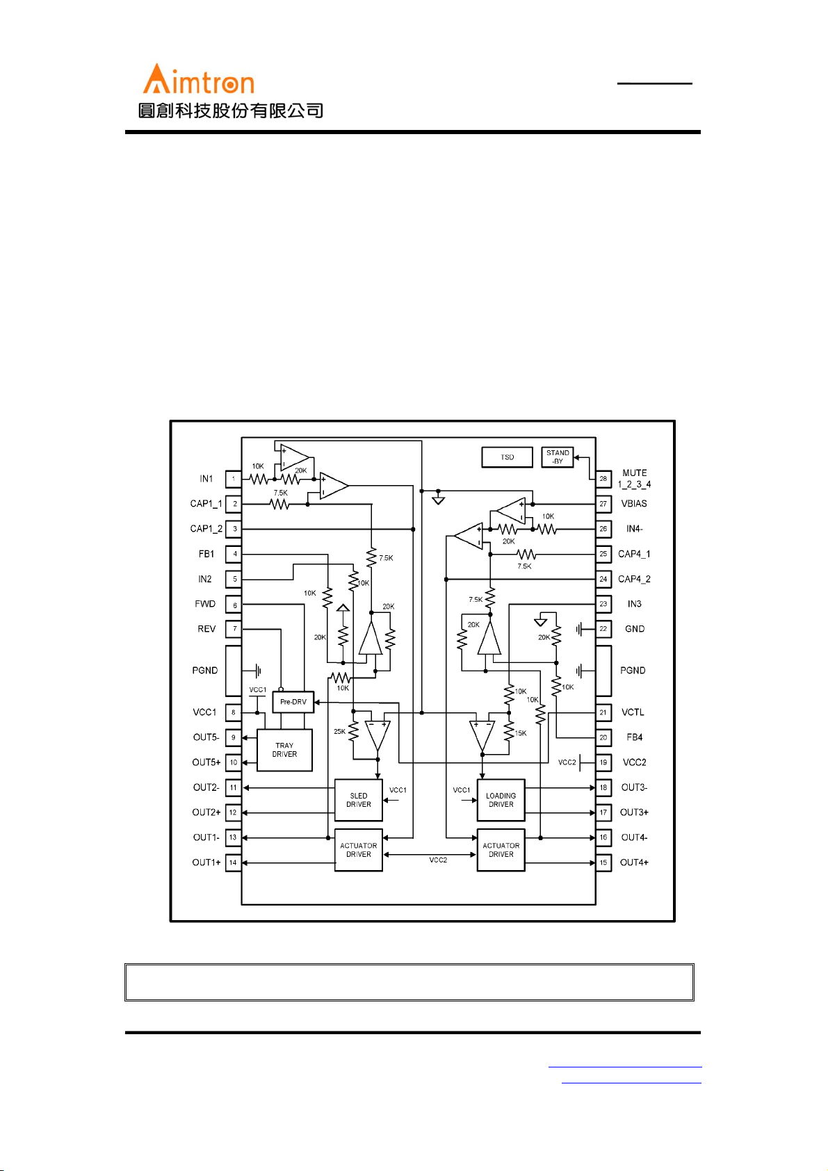
Block Diagram
Description
The AT5665 is a 5-channel BTL driver IC. Two
of them can drive DC motors and two can drive
coils, such as the focus and tracking actuators of
a CD-ROM/DVD-ROM/DVD-Player system,
with current feedback. It also built-in one
channel bi-direction DC motor driver for Tray.
Applications
CD-ROM/DVD-ROM/CD-RW drives
DVD player.
Aimtron reserves the right without notice to change this circuitry and specifications.
2F, No.10, Prosperity RD. II, Science-Based Industrial Park, Hsinchu 300,Taiwan, R.O.C.
Tel: 886-3-563-0878 http://www.aimtron.com.tw
Fax: 886-3-563-0879 Email: service@aimtron.com.tw
1
AT5665
Preliminary Product Information
5-Channel Motor Driver for DVD/VCD
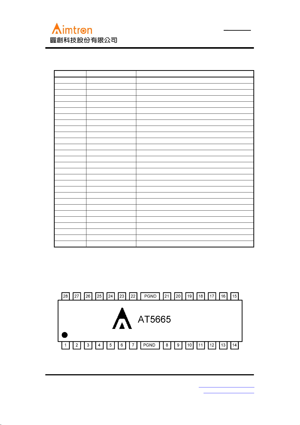
Pin Descriptions
Pin No.
1 IN1 CH1(Focus coil) input
2 CAP1_1 CH1 error amplifier filter capacitor connection 1
3 CAP1_2 CH1 error amplifier filter capacitor connection 2
4 FB1 CH1(Focus coil) feedback pin
5 IN2 CH2(Sled driver) input
6 FWD CH5 forward input
7 REV CH5 reverse input
8 VCC1 Power Supply 1
9 OUT5- CH5(Tray driver) output(-)
10 OUT5+ CH5(Tray driver) output(+)
11 OUT2- CH2(Sled driver) output (-)
12 OUT2+ CH2(Sled driver) output (+)
13 OUT1- CH1(Focus coil) output (-)
14 OUT1+ CH1(Focus coil) output (+)
15 OUT4+ CH4(Tracking coil) output (+)
16 OUT4- CH4(Tracking coil) output (-)
17 OUT3+ CH3(Loader) output (+)
18 OUT3- CH3(Loader) output (-)
19 VCC2 Power Supply 2
20 FB4 CH4(Tracking coil) feedback pin
21 VCTL CH5 Speed control input
22 GND Ground
23 IN3 CH3(Loader) input
24 CAP4_2 CH4 error amplifier filter capacitor connection 2
25 CAP4_1 CH4 error amplifier filter capacitor connection 1
26 IN4- CH4 (Tracking driver) input
27 VBIAS VREF input pin
28 MUTE_1_2_3_4 Mute control for CH1,Ch2,CH3,CH4
Notes: The indicated polarities for the output pins are under the condition that all inputs are (+).
The power supplies for the driver output are PVcc1 for the loader, PVcc2 for focus and tracking
drivers, and Vcc for pre-block and sled driver. Therefore, make sure Vcc≧PVcc1,2.
Pin name Function
Pin Out
2F, No.10, Prosperity RD. II, Science-Based Industrial Park, Hsinchu 300,Taiwan, R.O.C.
Tel: 886-3-563-0878 http://www.aimtron.com.tw
Fax: 886-3-563-0879 Email: service@aimtron.com.tw
2
AT5665
Preliminary Product Information
5-Channel Motor Driver for DVD/VCD
Ordering Information
Part number Package Marking
AT5665H 28-pin HSOP AT5665H
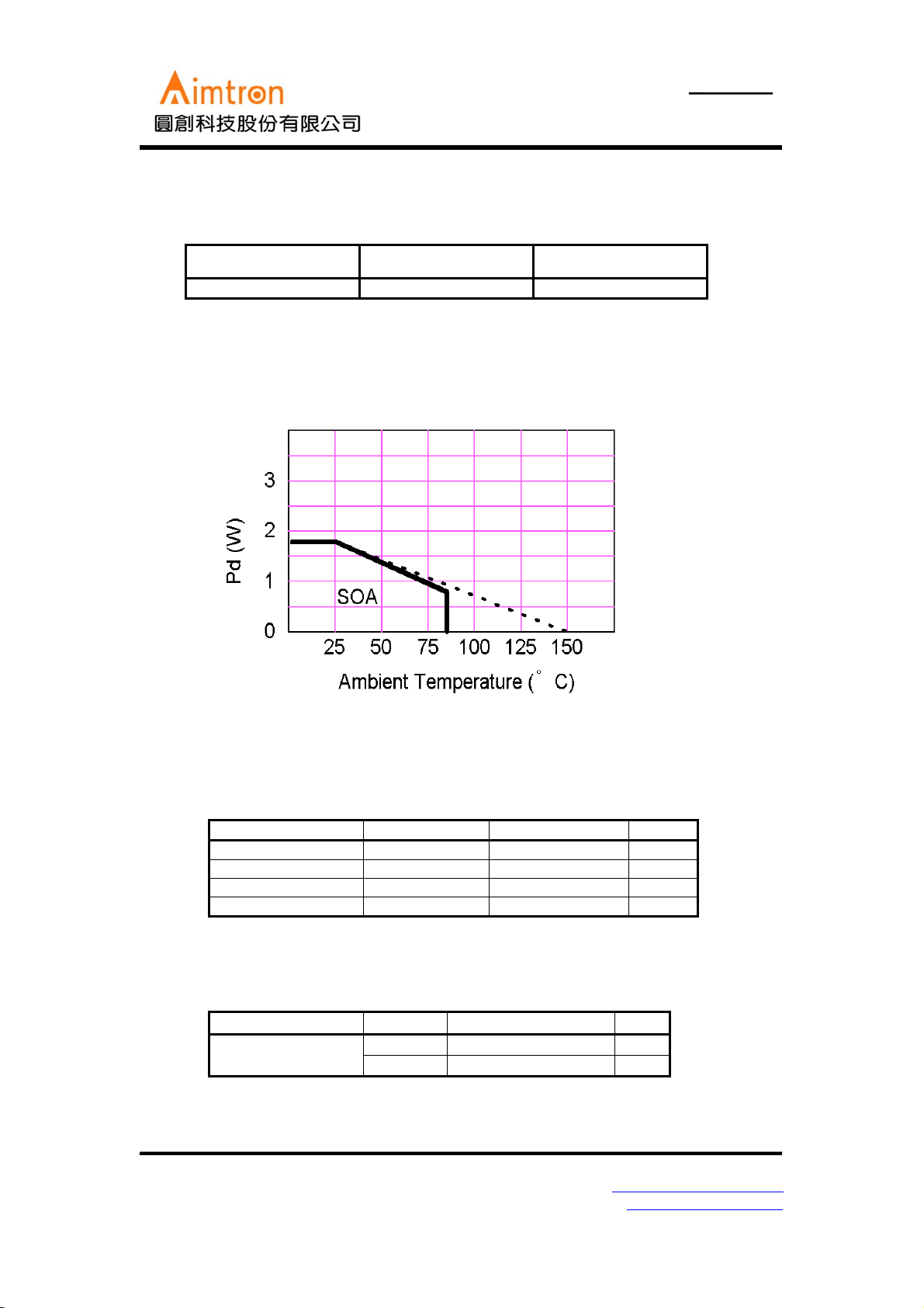
Power Dissipation (Ta = 25oC)
Condition: mount on 50x50 mm2 t=1.0mm paper phenol PCB
Absolute maximum ratings (Ta = 25oC)
Parameter Symbol Limits unit
Power supply voltage VCC1,2 13.5 V
Power dissipation P
Operating temperature T
Storage temperature T
NOTE:*
1. Power dissipation reduces 13.6mW / °C for using above Ta=25°C
2. Do not exceed Pd and SOA.
d
opr
stg
1.7 W
-30~+80
-55~+150
o
C
o
C
Recommended operating conditions (Ta = 25oC)
Parameter Symbol Limits unit
VCC1 4.0~13.2 VPower supply voltage
VCC2 4.0~Vcc1 V
2F, No.10, Prosperity RD. II, Science-Based Industrial Park, Hsinchu 300,Taiwan, R.O.C.
Tel: 886-3-563-0878 http://www.aimtron.com.tw
Fax: 886-3-563-0879 Email: service@aimtron.com.tw
3
AT5665
Preliminary Product Information
5-Channel Motor Driver for DVD/VCD
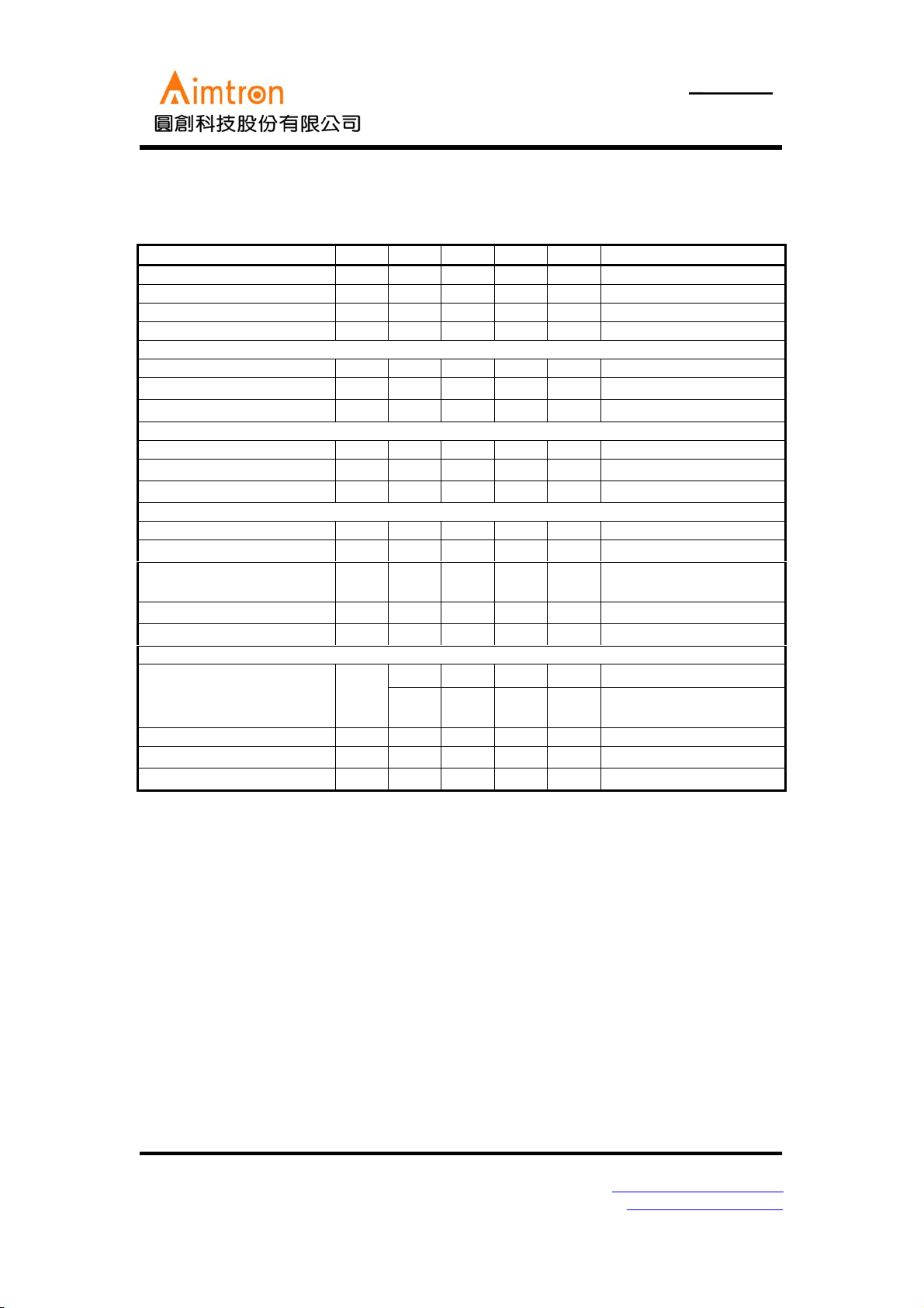
Electrical characteristics
(unless otherwise noted, Ta = 25
Parameter Symbol Min. Typ. Max. Unit Conditions
Quiescent current I
Mute quiescent current I
Mute ON voltage V
Mute OFF voltage V
<Actuator driver>
Output current offset I
Maximum output voltage V
Gain Gm 1.3 1.5 1.7 A/V
<Sled motor driver>
Output voltage offset V
Maximum output voltage V
Closed loop gain G
<Loader motor driver>
Output voltage offset V
Maximum output voltage V
Maximum output voltage V
Closed loop gain G
Gain error
<Tray motor driver>
Maximum output voltage V
Output voltage offset V
Input high level voltage V
Input low level voltage V
o
C,VCC1 =12V, VCC2 =5V, VBIAS=2.5V, RL1= RL2=8Ω, RL3= RL4=12Ω)
QC
QSB
SBON
SBOFF
O1,2
O1,2
OFFSL
O3MAX
VSL
OFFLD
O4max1
O4max2
-1827mANo Load
- - 5 mA CH5 active
0-0.5V
2.0 - - V
-6 - 6 mA
3.6 4.0 - V
= V
V
V
BIAS
IN
= V
BIAS
IN
-100 0 100 mV
7.5 9.0 - V
18.0 20.0 22.0 dB
= V
V
IN
BIAS
= V
V
BIAS
IN
-50 0 50 mV
7.5 9.0 - V
3.6 4.0 - V
= V
V
V
BIAS
IN
= V
BIAS
IN
VCC1=5V
ΔG
O5max1
13.5 15.5 17.5 dB
VLD
012dB
VLD
-6.0- V
3.8 - 4.2 V
= V
V
V
BIAS
IN
= V
BIAS
IN
RL5=45Ω, R
RL5=45Ω, R
VCC1=VCC2=5V
OFFTR
-50 0 50 mV
2.0 - - V
IH
IL
--0.8V
±1.5V
±0.2V
±1.5V
±0.2V
±2.0V
±1.5V
±0.2V
±0.2V
VCTL
VCTL
=400Ω,
=0Ω,
2F, No.10, Prosperity RD. II, Science-Based Industrial Park, Hsinchu 300,Taiwan, R.O.C.
Tel: 886-3-563-0878 http://www.aimtron.com.tw
Fax: 886-3-563-0879 Email: service@aimtron.com.tw
4
 Loading...