

Aimtron AT1396A, AT1396B, AT1396C, AT1396D User Manual
p
查询AT1396供应商查询AT1396供应商
Preliminary Product Information
Features
• 95% Efficient possible DC/DC Converter
• Combine Step-Up and Step-Down for
90% Efficient Boost-Buck
• Bulit-in LED Driver and Open LED
Overvoltage Protection
• Transformerless Inverting Controller for CCD
Bias
• 2 Channel Built-in MOSFET Current- Mode
PWM and 4 Channel Extra PWM Controllers
(CH-3 Synchronous Output)
• Up to 1MHz Operating Frequency
• Shutdown Current <1uA
• Built-in Soft-Start Function
• Built-in Short-Circuit Protection Function
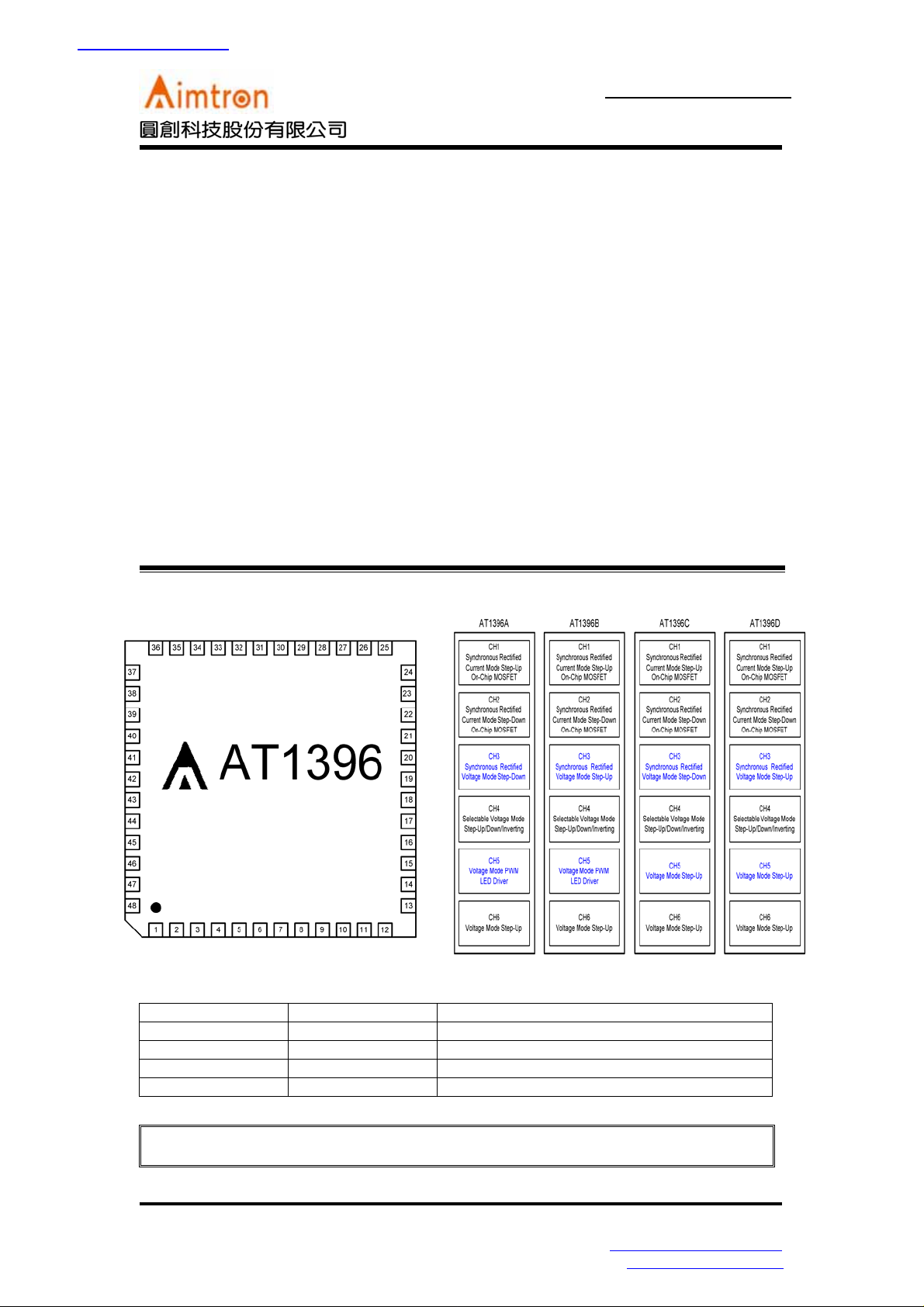
• QFN48 Package
Applications
• DSC Power Supply
AT1396A/B/C/D
6-Channel DC-DC Converter for DSC
General Description
The AT1396A/B/C/D provide a complete power
supply solution for digital cameras. They improve
erformance, component count, and size compared
to other multi-channel controllers in 2-cell AA,
1-cell Li-Ion, and dual-battery designs. On-chip
MOSFETs provide up to 92~95% efficiency for
critical power supplies, while additional channels
operate with external FETs for optimum design
flexibility. All channels DC/DC operate at one
fixed frequency settable from 100KHz to 1MHz to
optimize size, cost, and efficiency.
Pin Assignment
Ordering Information
Part Number Package Marking
AT1396AN QFN48,Green AT1396AN
AT1396BN QFN48,Green AT1396BN
AT1396CN QFN48,Green AT1396CN
AT1396DN QFN48,Green AT1396DN
Aimtron reserves the right without notice to change this circuitry and specifications.
2F, No.10, Prosperity RD. II, Science-Based Industrial Park, Hsinchu 300,Taiwan, R.O.C.
Tel: 886-3-563-0878 WWW: http://www.aimtron.com.tw
Fax: 886-3-563-0879 Email: service@aimtron.com.tw
1 REVD: 05/05/23
AT1396A/B/C/D
Preliminary Product Information
6-Channel DC-DC Converter for DSC
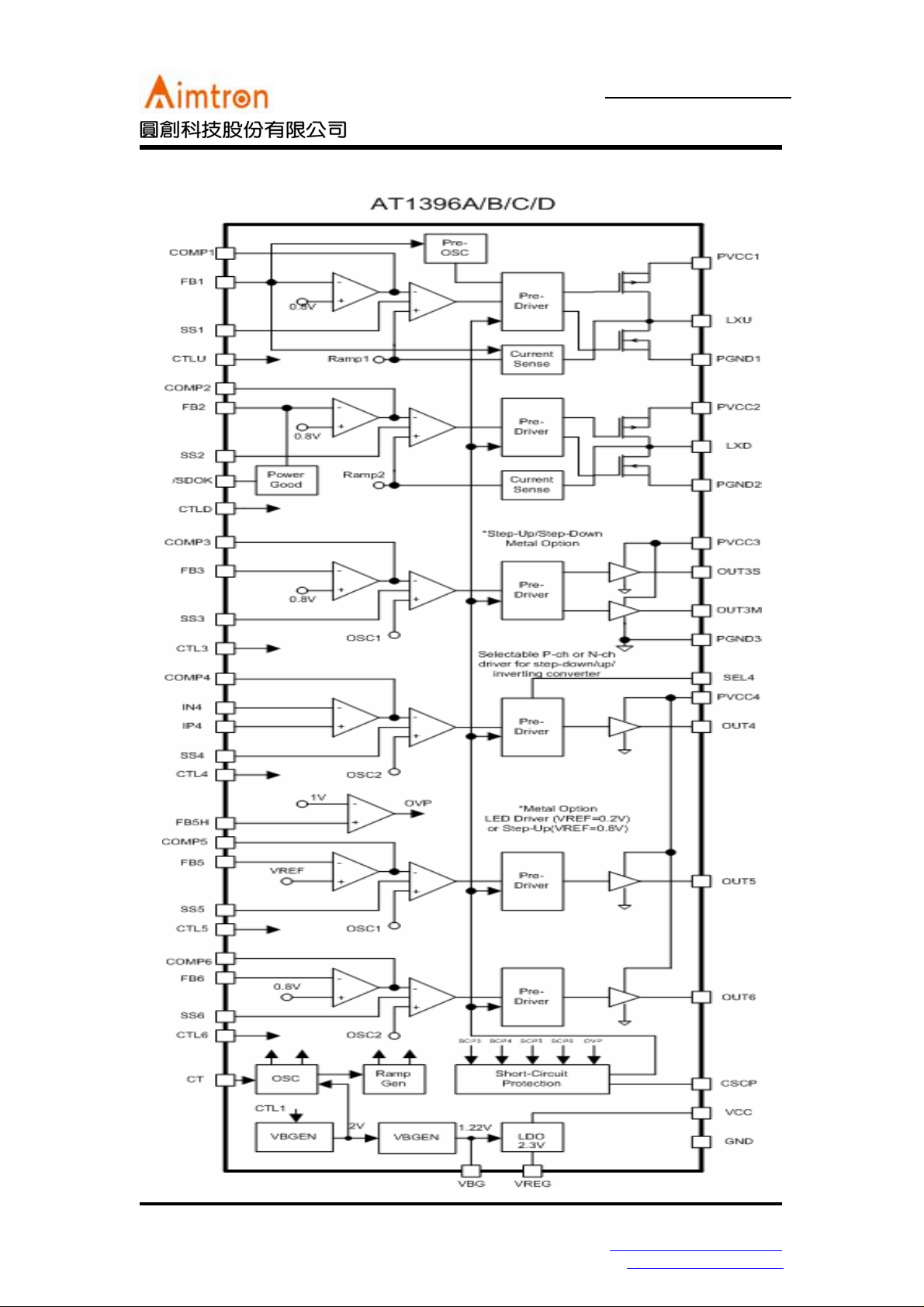
Block Diagram
2F, No.10, Prosperity RD. II, Science-Based Industrial Park, Hsinchu 300,Taiwan, R.O.C.
Tel: 886-3-563-0878 WWW: http://www.aimtron.com.tw
Fax: 886-3-563-0879 Email: service@aimtron.com.tw
2 REVD: 05/05/23
AT1396A/B/C/D
Preliminary Product Information
6-Channel DC-DC Converter for DSC
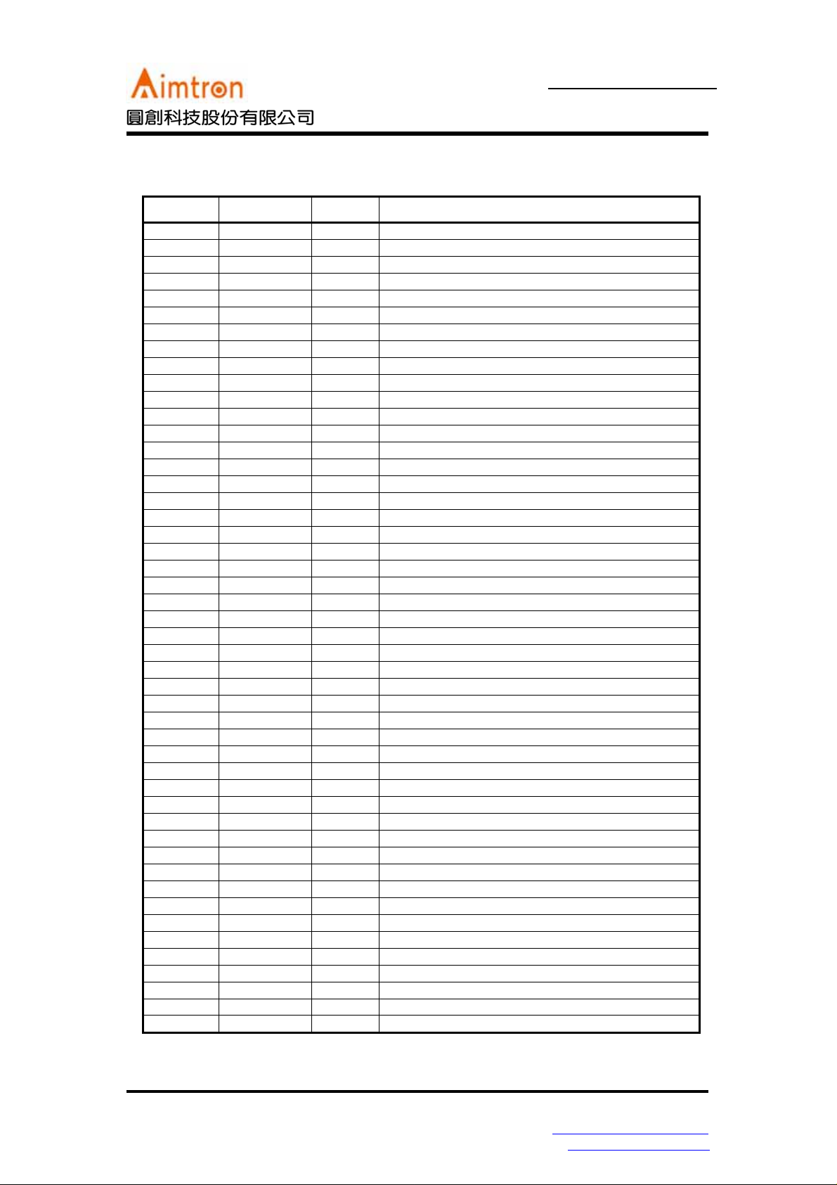
Pin Description
Pin No. Pin name I/O Description
1 SS1 I CH1 Soft-Start Input
2 CTL5 I CH5 Enable Input
3 CTL6 I CH6 Enable Input
4 LXU O Step-Up Converter Switching Node
5 CTLU I CH1 Enable and Chip Enable Input
6 PGND1 P Power Ground
7 PGND2 P Power Ground
8 CTLD I CH2 Enable Input
9 LXD O Step-Down Converter Switching Node
10 CTL3 I CH3 Enable Input
11 CTL4 I CH4 Enable Input
12 SS2 I CH2 Soft-Start Input
13 /SDOK O Open-Drain, Active Low, Power Good for Step-Down
14 CSCP I Short Circuit Protection Input
15 PVCC2 P Step-Down Converter Input
16 COMP2 O Step-Down Converter Compensation Node
17 FBD I Step-Down Converter Feedback Input
18 SS3 I CH3 Soft-Start Input
19 COMP3 O CH3 Compensation Node
20 FB3 I CH3 Feedback Input
21 SS4 I CH4 Soft-Start Input
22 COMP4 O CH4 Compensation Node
23 IN4 I CH4 Negative Feedback Input
24 IP4 I CH4 Positive Feedback Input
25 PVCC3 P CH3 Power
26 OUT3M O CH3 Master Output Driver
27 OUT3S O CH3 Slave Output Driver
28 PGND3 P Power Ground
29 OUT4 O CH4 Output Driver
30 OUT5 O CH5 Output Driver
31 OUT6 O CH6 Output Driver
32 PVCC4 P CH4 Power
33 GND P Power Ground
34 FB5H I CH5 Controller Voltage Feedback Input
35 FB5 I CH5 Controller Voltage Feedback/Current Feedback
36 COMP5 O CH5 Compensation Node
37 VBG O Reference Bypass
38 SS5 I CH5 Soft-Start Input
39 FB6 I CH6 Feedback input
40 COMP6 O CH6 Compensation Node
41 CT O Oscillator Control
42 VREG P Reference Output
43 FBU I Step-Up Converter Input
44 COMP1 O Step-Up Controller Compensation Node
45 VCC P IC power Input
46 PVCC1 P Power Output of the Step-Up Converter
47 SS6 I CH6 Soft-Start Input
48 SEL4 I Configures the CH4 as a Step-Up or Step-Down
2F, No.10, Prosperity RD. II, Science-Based Industrial Park, Hsinchu 300,Taiwan, R.O.C.
Tel: 886-3-563-0878 WWW: http://www.aimtron.com.tw
Fax: 886-3-563-0879 Email: service@aimtron.com.tw
3 REVD: 05/05/23
AT1396A/B/C/D
Preliminary Product Information
6-Channel DC-DC Converter for DSC
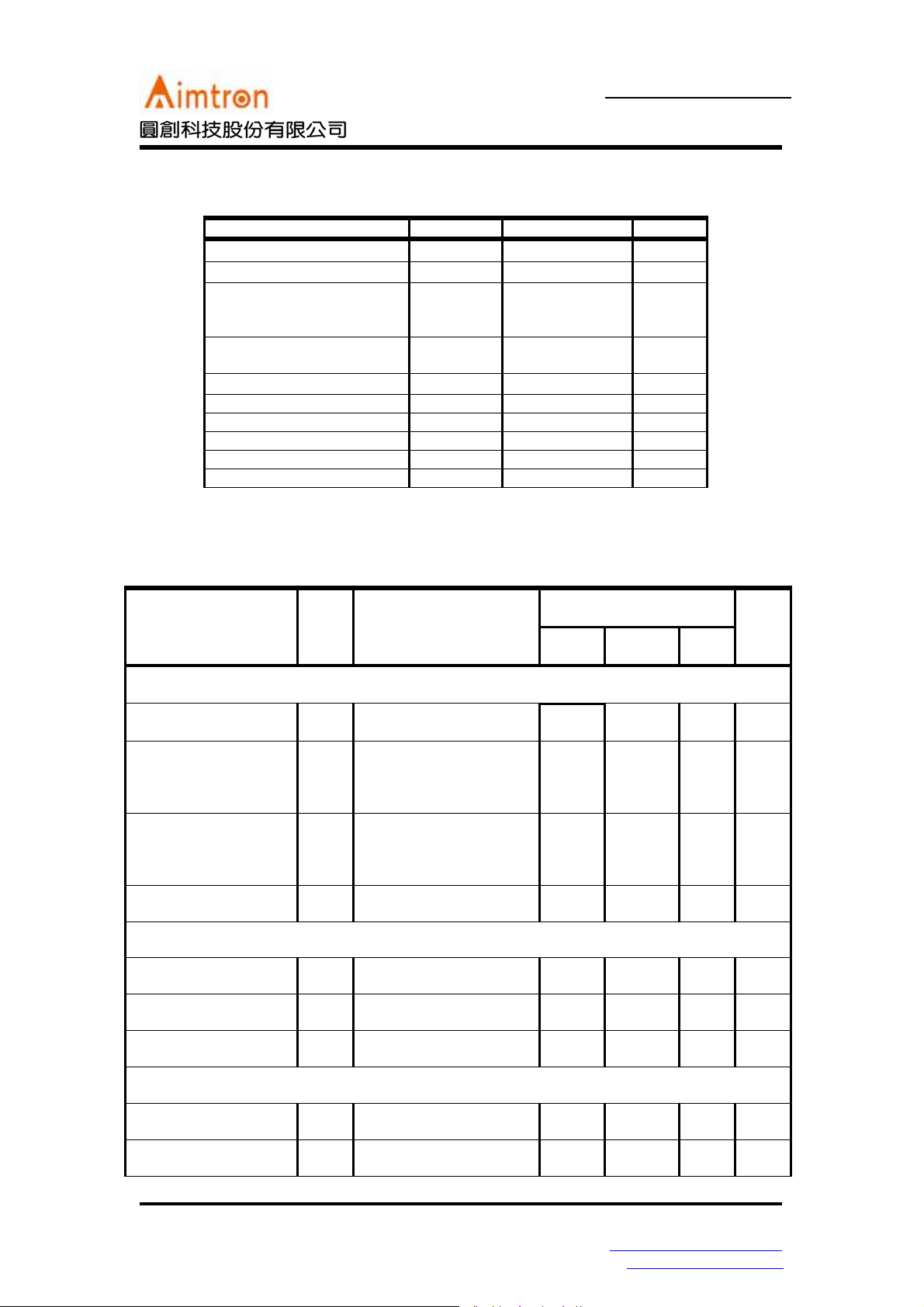
Absolute Maximum Ratings
Item Symbol Ratings Units
Storage temperature T
Operating temperature T
STG
OPR
PVCC1,PVCC2,PVCC3,PVCC
4 input voltage
LXU,LXD, OUT3M,OUT3S
V
LX/OUT
input voltage
Other input Pin
LXU Current 3.6 A
LXD Current 2.25 A
OUT3M,OUT3S Current 200 mA
Power consumption Pd 1000 mW
ESD Classification 2 KV
-55~+150 ℃
-30~+85 ℃
-0.3~+5.5
-0.3V~+5.5
-0.3V~+5.5
V
V
V
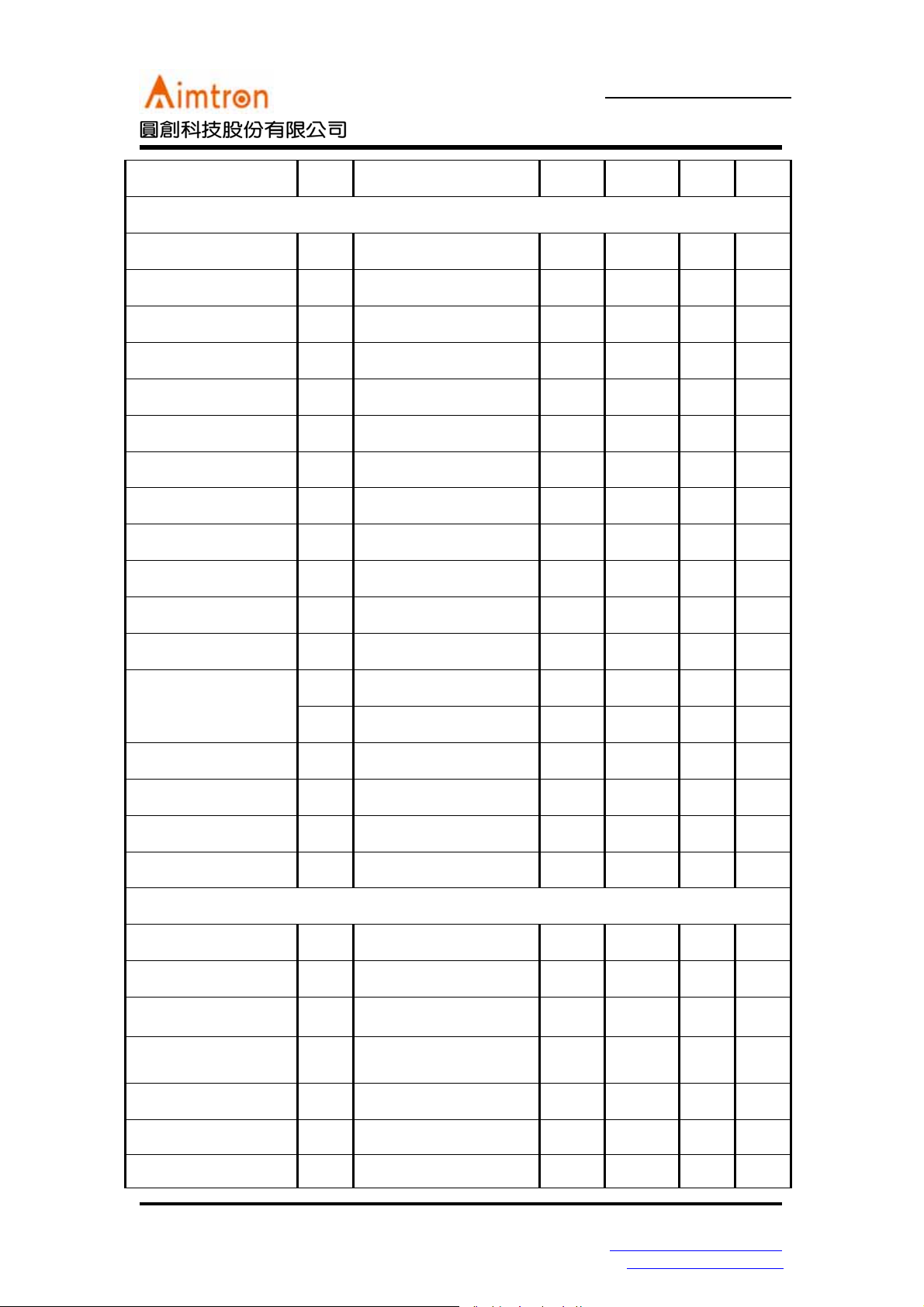
Electrical Characteristics
(PVCC1=PVCC2=PVCC3=PVCC4=VCC=3.6V, Ta=+25
Values
Parameter Symbol Condition
Unit
Min. Typ. Max.
GENERAL
Input Voltage R ange VCC Channel 1 DC/DC 1.2 - 5.5 V
No Switching,
CH1,CH2
Switch- Off Input Current
FBU=FBD=0.9V
I
VCC
CTLU=CTLD=3.6V,other
- 1 1.1 mA
disable
No Switching,
CH1,CH2, CH3(or 4,5,6)
Switch- Off Input Current
FBU=FBD=FB3=0.9V
I
VCC
CTLU=CTLD=CTL3=3.6V
- 1.2 1.3 mA
other disable
Shutdown Current I
All CTL disable - 1 10
VCC
μA
REFERENCE
Reference Output Voltage V
Reference Load
Regulation
∆V
REG IREG
REG1
=1mA 2.275 2.30 2.325 V
1mA< I
<10mA - 5 10 mV
REG
0
C)
Reference Line Regulation
∆V
2.5<VCC<5.5V - - 5 mV
REG2
OSC
Frequency f
Frequency variation with
Temperature
2F, No.10, Prosperity RD. II, Science-Based Industrial Park, Hsinchu 300,Taiwan, R.O.C.
Tel: 886-3-563-0878 WWW: http://www.aimtron.com.tw
Fax: 886-3-563-0879 Email: service@aimtron.com.tw
CT=82pF - 500 - KHz
OSC
∆f
Ta=-20°C ~+85°C
OSC1
- 1 10 %
4 REVD: 05/05/23
AT1396A/B/C/D
Preliminary Product Information
6-Channel DC-DC Converter for DSC
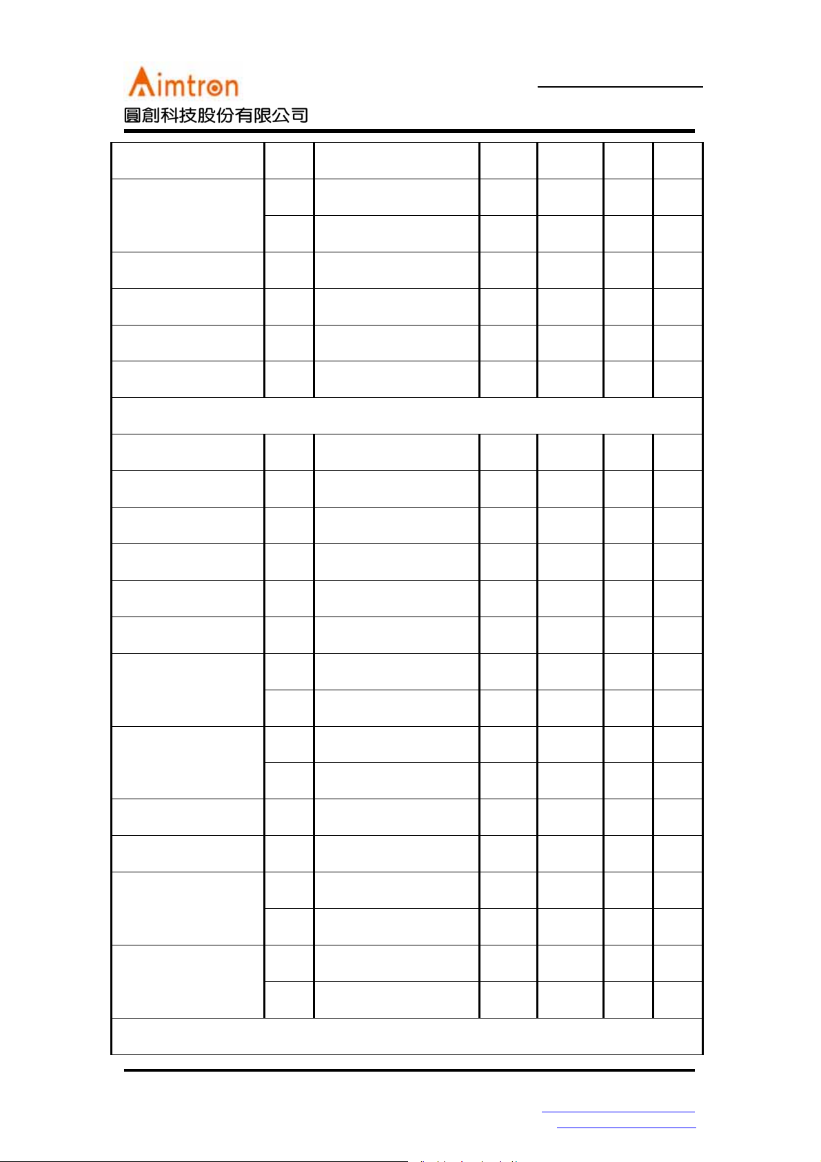
Frequency variation with
Input Voltage
∆f
OSC2
CHANNEL 1(STEP-UP)
Pre-OSC to OSC Trip
Level
Pre-OSC to OSC
Hysteresis
Under Voltage Lockout VCC - 2.45 - V
Input Voltage Ra nge PVCC1 Channel 1 DC/DC 1.2 - 6.0 V
V
CC1
∆VCC1
=2.5V~5.5V - 1 5 %
V
CC
VCC rising edge - 2.45 - V
- 100 - mV
Normal Operating
Soft-Start Charge Current
FBU Regulation Voltage V
FBU input Current I
Current-Sense Amplifier
Transresistance
Transconductance G
Maximum Duty Cycle D
I
SS1
FBU
R
MEA
MAX
FBU
CS
PVCC1 Leakage Current IL1
LX Leakage Current I
LX1
RN N-Channel - 95 150
Switch On-Resistance
R
N-Channel Current Limit I
P-Channel Turn-off
Current
Startup Current Limit I
Limit1
I
REV1
Limit-s
VCC =2.5V~5.5V 0.8 1 1.5
Ta=-20°C ~+85°C
0.784 0.8 0.816 V
µA
FBU=0.8V - - 100 nA
- 0.285 - V/A
- 140 -
µs
FBU=0.7V 85 90 95 %
V
=0V,PVCC1=5.5V
LXU
V
LXU
=5.5V
- 5 12
- 1 5
µA
µA
mΩ
P-Channel - 150 250
P
mΩ
1.8 2.1 2.4 A
- 20 - mA
PVCC1=1.5V - 450 - mA
Startup Frequency f
PVCC1=1.5V - 200 - KHz
START
CHANNEL 2(STEP-DOWN)
Input Voltage Ra nge PVCC2 Channel 2 DC/DC 1.2 - 6.0 V
Normal Operating
Soft-Start Charge Current
FBD Regulation Voltage V
FBD input Current I
Current-Sense Amplifier
Transresistance
Transconductance G
Maximum Duty Cycle D
2F, No.10, Prosperity RD. II, Science-Based Industrial Park, Hsinchu 300,Taiwan, R.O.C.
Tel: 886-3-563-0878 WWW: http://www.aimtron.com.tw
Fax: 886-3-563-0879 Email: service@aimtron.com.tw
I
VCC =2.5V~5.5V 0.8 1 1.5
SS2
Ta=-20°C ~+85°C
FBD
FBD=0.8V - - 100 nA
FBD
R
- 0.6 - V/A
CS
- 140 -
MEA
FBD=0.7V - 100 - %
MAX
0.784 0.8 0.816 V
5 REVD: 05/05/23
µA
µs
AT1396A/B/C/D
Preliminary Product Information
6-Channel DC-DC Converter for DSC
LX Leakage Current I
VLX=0~3.6V,PVCC2=3.6V
LX2
- 1 5
RN N-Channel - 95 150
µA
mΩ
Switch On-Resistance
R
P-Channel Current Limit I
N-Channel Turn-off
Current
/SDOK Output Low
Voltage
/SDOK Leakage current I
P-Channel - 150 250
P
1.0 1.2 1.4 A
Limit2
I
- 20 - mA
REV2
V
0.1mA into /SDOK - 0.01 0.1 V
SDOK
CTLD=0V,/SDOK=5.5V - 0.1 1
L_SDOK
mΩ
µA
CHANNEL 3
Input Voltage Ra nge PVCC3 Channel 3 DC/DC 1.2 - 6.0 V
Normal Operating
Soft-Start Charge Current
FB3 input Current I
FB3 Regulation Voltage V
Error Amplifier V oltage
Gain
Error Amplifier Frequency
Bandwidth
I
VCC =2.5V~5.5V 0.8 1 1.5
SS3
FB3=0.8V - - 100 nA
FB3
Ta=-20°C ~+85°C,
FB3
FB3=COMP3
0.784 0.8 0.816 V
µA
AV DC 80 - - dB
BW AV=0dB - 5 - MHz
Error Amplifier Output
Voltage
Error Amplifier Output
Source Current
Output Source Current
Output Sink Current
Output On-Resistor
Maximum Duty Cycle
CHANNEL 4,5,6
V
VOL
I
I
D
D
- 1.0 - V
OH
- 10 - mV
COMP=0.8V - -0.5 - mA
source
I
COMP=0.8V - 60 -
sink
DUTY=90%,OUT=1/2VCC - -130 -80 mA
source
I
DUTY=0%,OUT=1/2VCC 65 100 - mA
sink
ROH
OUT=-15mA - 18 30
R
OUT=15mA - 16 25
OL
Step-Up Mode 85 90 95 %
MAX
Step-Down Mode - 100 - %
MAX
µA
Ω
Ω
2F, No.10, Prosperity RD. II, Science-Based Industrial Park, Hsinchu 300,Taiwan, R.O.C.
Tel: 886-3-563-0878 WWW: http://www.aimtron.com.tw
Fax: 886-3-563-0879 Email: service@aimtron.com.tw
6 REVD: 05/05/23
AT1396A/B/C/D
Preliminary Product Information
6-Channel DC-DC Converter for DSC
Input Voltage R ange PVCC4 Channel 4,5,6 DC/DC 1.2 - 6.0 V
Normal Operating
Soft-Start Charge Current
FB4/5/6 Regulation
Voltage
V
FB5 Regulation Voltage
for LED Driver
FB5H OVP Trip Level V
Error Amplifier V oltage
Gain
Error Amplifier Frequency
Bandwidth
Error Amplifier Output
Voltage
Error Amplifier Output
Source Current
Maximum Duty Cycle
I
SS4/5/6 VCC
FB4/5/6
V
FB5
FB5H
=2.5V~5.5V 0.8 1 1.5
Ta=-20°C ~+85°C,
FB_=COMP_
Ta=-20°C ~+85°C,
FB5=COMP5
Ta=-20°C ~+85°C,
0.784 0.8 0.816 V
0.19 0.20 0.21 V
0.98 1.00 1.02 V
µA
AV DC 80 - - dB
BW AV=0dB - 5 - MHz
V
VOL
I
D
D
- 1.0 - V
OH
- 10 - mV
COMP=0.8V - -0.5 - mA
source
I
COMP=0.8V - 60 -
sink
FB_=0.7V 85 90 95 %
MAX
FB5=0.1V 85 90 95 %
MAX
µA
Output Source Current
Output Sink Current
I
DUTY=90%,OUT=1/2VCC - -130 -80 mA
source
I
DUTY=0%,OUT=1/2VCC 65 100 - mA
sink
ROH
OUT=-15mA - 18 30
Output On-Resistor
R
OUT=15mA - 16 25
OL
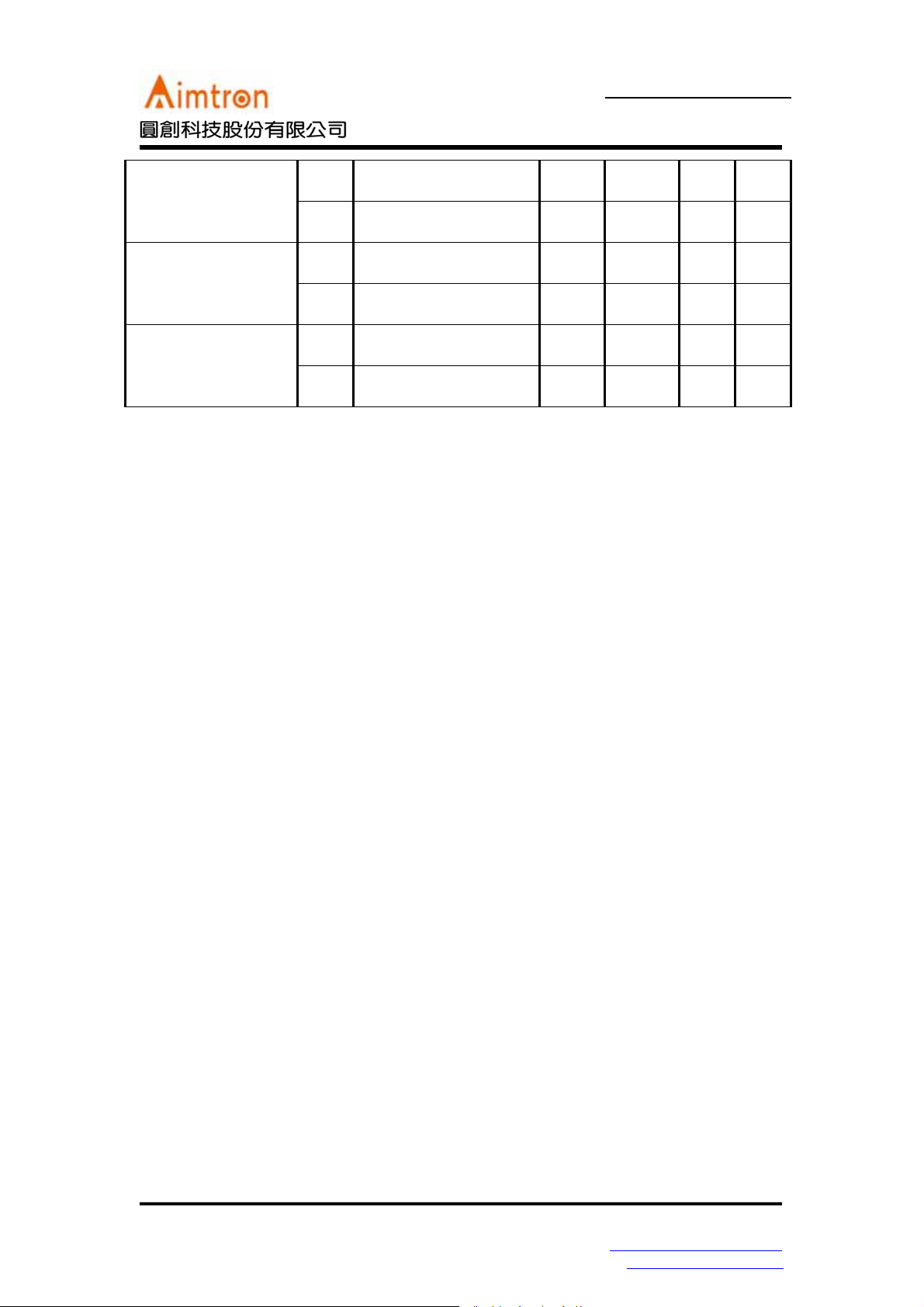
SHORT CIRCUIT PROTECTION
V
Threshold Voltage
CSCP Charge Current
I
CH3,CH4,CH5,CH6 - 0.9 - V
TH
0.8 1.0 1.5
CSCP
CONTROL BLOCK
VIH
PVCC1=VCC=1.5 ~5.5V 1.1 - VCC V
CTLU input Voltage
V
PVCC1=VCC=1.5 ~5.5V 0 - 0.5 V
IL
PVCC1 , 2=VCC=1.5 ~5.5V
VIH
CTLD input Voltage
CTLD=V
PVCC1 , 2=VCC=1.5 ~5.5V
V
IL
CTLD=V
IH
IH
Ω
Ω
µA
1.1 - VCC V
0 - 0.5 V
2F, No.10, Prosperity RD. II, Science-Based Industrial Park, Hsinchu 300,Taiwan, R.O.C.
Tel: 886-3-563-0878 WWW: http://www.aimtron.com.tw
Fax: 886-3-563-0879 Email: service@aimtron.com.tw
7 REVD: 05/05/23
AT1396A/B/C/D
Preliminary Product Information
6-Channel DC-DC Converter for DSC
PVCC1 , 3=VCC=1.5 ~5.5V
CTL3 input Voltage
CTL4 , 5 , 6 input Voltage
SEL4 input Voltage
VIH
CTLU=V
PVCC1 , 3=VCC=1.5 ~5.5V
V
IL
CTLU=V
PVCC1 , 4=VCC=1.5 ~5.5V
VIH
CTLU=V
PVCC1 , 4=VCC=1.5 ~5.5V
V
IL
CTLU=V
PVCC1 , 4=VCC=1.5 ~5.5V
VIH
CTLU=CTL4=V
PVCC1 , 4=VCC=1.5 ~5.5V
V
IL
CTLU=CTL4=V
IH
IH
IH
IH
IH
IH
1.4 - VCC V
0 - 0.5 V
1.4 - VCC V
0 - 0.5 V
1.4 - VCC V
0 - 0.5 V
2F, No.10, Prosperity RD. II, Science-Based Industrial Park, Hsinchu 300,Taiwan, R.O.C.
Tel: 886-3-563-0878 WWW: http://www.aimtron.com.tw
Fax: 886-3-563-0879 Email: service@aimtron.com.tw
8 REVD: 05/05/23
 Loading...