

AIM AT1732 Datasheet
AT1732
Preliminary
2-Channel PWM Controller for LCD Bias
2F, No.10, Prosperity RD. II, Science-Based Industrial Park, Hsinchu 300,Taiwan, R.O.C.
Tel: 886-3-563-0878 WWW: http://www.aimtron.com.tw
Fax: 886-3-563-0879 Email: service@aimtron.com.tw
1
Features
• Low input voltage: 2.5V to 7V
• 2-Channels PWM Control:
2 Boost Controller(CH1,CH2)
• Adjustable Soft start time and maximum duty
cycle
• Built-in timer latch for short circuit protection:
Delay time=216/(Switching frequency)
• Built-in under-voltage lockout, thermal
shutdown.
• High operating frequency: 100kHz to 1MHz
Applications
• LCD Displays Bias
• Power Supply for general equipment
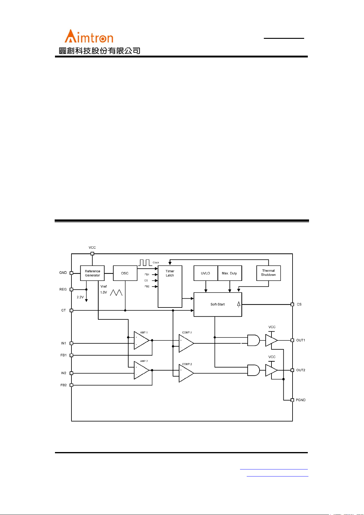
General Description
The AT1732 is a PWM DC/DC converter control
IC with 2 channel outputs that can directly drive
power MOSFET. This IC ia suitable for very small
DC/DC converters because of their small and thin
package(1.1 mm max.), and high operation
frequency (up to 1.0 MHz).
Block Diagram
AT1732
Preliminary
2-Channel PWM Controller for LCD Bias
2F, No.10, Prosperity RD. II, Science-Based Industrial Park, Hsinchu 300,Taiwan, R.O.C.
Tel: 886-3-563-0878 WWW: http://www.aimtron.com.tw
Fax: 886-3-563-0879 Email: service@aimtron.com.tw
2
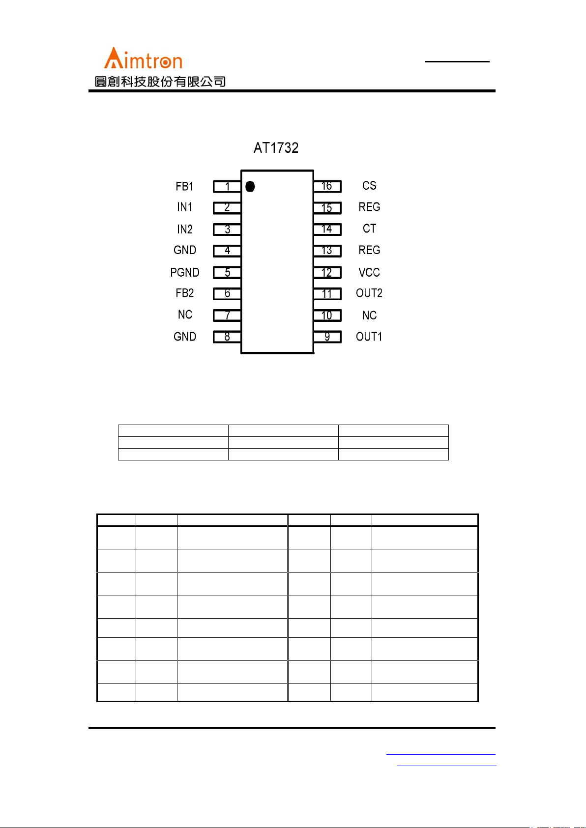
Pin Configuration
Ordering Information
Part number Package Marking
AT1732 TSSOP16 AT1732P
-
Pin Description
Symbol Pin No. Descript Symbol Pin No. Descript
FB1
1 CH1 error amplifier output
OUT1
9 CH1 output for Nch-
MOSFET
IN1
2 CH1 inverting input to
error amplifier
NC
10
Don’t connect
IN2
3
CH2 inverting input to
error amplifier
OUT2
11 CH2 output for Nch-
MOSFET
GND
4 Control blocks ground
VCC
12 Power Supply
PGND
5 Power blocks ground
REG
13 Regulated voltage output
FB2
6 CH2 error amplifier output
CT
14 Oscillator timing
capacitor
NC
7
Don’t connect
REG
13 Regulated voltage output
Connect to pin13
NC
8
Don’t connect CS
16 Soft-star for CH1/2
AT1732
Preliminary
2-Channel PWM Controller for LCD Bias
2F, No.10, Prosperity RD. II, Science-Based Industrial Park, Hsinchu 300,Taiwan, R.O.C.
Tel: 886-3-563-0878 WWW: http://www.aimtron.com.tw
Fax: 886-3-563-0879 Email: service@aimtron.com.tw
3
Absolute Maximum Ratings
Rated ValueParameter Condition
Min. Max.
Unit
Power Supply Voltage — - +8 V
Source Average Current of OUT1
OUT2,
—--50mA
Sink Average Current of OUT1
OUT2
—-50mA
Input Voltage to Error Amplifier — - 6.5 V
Continuous power dissipation
TSSOP16(Ta=+25℃)
-500mW
Operating temperature — -30 +85
0
C
Junction temperature — - +125
0
C
Storage temperature — -40 +150
0
C
Lead temperature — - +300
0
C
Stresses beyond those listed under “Absolute Maximum Ratings” may cause permanent damage to the device. These are
stress ratings only, and functional operation of the device at these or any other conditions beyond those indicated in the
operational sections of the specifications is not implied. Exposure to absolute maximum rating conditions for extended
periods may affect device reliability.
Recommended Operating Conditions
(Ta=+250C)
Va lu esParameter Symbol
Min. Typ. Max.
Unit
Power supply voltage V
CC
2.5 -- 7
V
Oscillation frequency f
OSC
100 500 1000 KHz
Operating temperature T
OP
-30 +25 +85 °C
 Loading...