

AIC AIC1117-50CY, AIC1117-50CT, AIC1117-50CM, AIC1117-50CE, AIC1117-33CY Datasheet
...
1%
1%
AIC1
117-28
AIC1117
800mA Low Dropout Positive Adjustable
Regulator
FEATURES
n
l Dropout Voltage 1. 2V at 800mA Output Current.
l Fast Transient Response.
l Line Regulation typically at 0.015%.
l Load Regulation typically at 0.1%.
l Internal Thermal and Current Limiting.
l Adjustable Output Voltage or Fixed 2.85V, 3.3V,
5V.
l Standard 3-Pin Power Packages.
APPLICATIONS
n
l SCSI-2 Active Terminator.
l Post Regulator for Switching Supply.
l Battery Chargers.
l Constant-Current Regulators.
l PC Add-On Card.
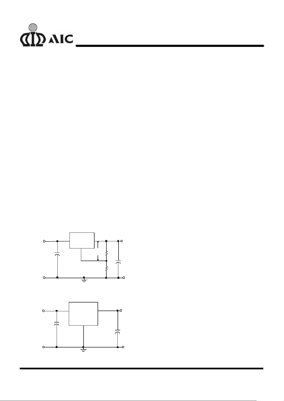
TYPICAL APPLICATION CIRCUIT
n
DESCRIPTION
n
The AIC1117 is a low dropout three terminal
regulator with 800mA output current capability.
The output voltage is adjustable with the use
of a resistor divider. For fixed output voltage
versions, the output voltage is internally set at
2.85V, 3.3V or 5V. Dropout is guaranteed at a
maximum of 1. 3V at maximum output current.
Its low dropout voltage and fast transient
response make it ideal for low voltage
microprocessor applications. Internal current
and thermal limiting provides protection
against any overload condition that would
create excessive junction temperatures.
V
5V
V
REF=VOUT
V
OUT=VREF
I
=55µA (typ.)
ADJ
(1) C1 needed if device is far away from filter
ADJ
23
RF2
205
REF
VOUT
3.3V
RF1
Ω
125
+
C2
Ω
10µF
IN
+ V
C1
10µF
AIC1117
1
- V
ADJ
x (1+RF2/RF1)+ I
capacitors.
=1.25V (typ.)
ADJ
x RF2
(2) C2 required for stability.
Adjustable Voltage Regulator
V
5V
IN
C1
10µF
3
AIC1117-33
+
AIC1117-50
1
GND
2
+
C2
10µF
V
OUT
Fixed Voltage Regulator
Analog Integrations Corporation 4F, 9, Industry E. 9th Rd, Science Based Industrial Park, Hsinchu Taiwan, ROC www.analog.com.tw
DS-1117-00 Mar 13, 00 TEL: 886-3-5772500 FAX: 886-3-5772510 1
ORDERING INFORMATION
231
123
231
231
n
AIC1117
AIC1 117-XXXX
PACKAGING TYPE
E: TO-252
M: TO-263
T: TO-220
Y: SOT-223
TEMPERATURE RANGE
C: 0°C~+70°C
OUTPUT VOLTAGE
DEFAULT: ADJ.
28: 2.85V
33: 3.3V
50: 5.0V
ORDER NUMBER
AIC1117C E
(TO-2 52)
AIC1 117CM
(TO-263)
AIC1117CT
(TO-220)
AIC1117CY
(SOT-223)
PIN CONFIGURATION
FRONT VIEW
1: ADJ (GND)
2: VOUT (TAB)
3: VIN
FRONT VIEW
1: ADJ (GND)
2: VOUT (TAB)
3: VIN
FRONT VIEW
1: ADJ (GND)
2: VOUT (TAB)
3: VIN
FRONT VIEW
1: ADJ (GND)
2: VOUT (TAB)
3: VIN
ABSOLUTE MAXIMUM RATINS
n
VIN pin to ADJ/ GND pin ...........................…….......…….....…………............................ 7V
Operating Junction Temperature Range ..................………...................... 0°C ~ 125°C
Storage Temperature Range ...............................…………................. - 65°C ~ 150 °C
Thermal Resistance (Junction to Case) TO-220 ………........……...…………... 3°C /W
TO-252 …....……....………………..12.5°C /W
SOT-223 …....……..………..………..15°C /W
Lead Temperature (Soldering) 10 sec. .....................………............………...….......260°C
TEST CIRCUIT
n
Refer to TYPICAL APPLICATION CIRCUIT.
2
AIC1117
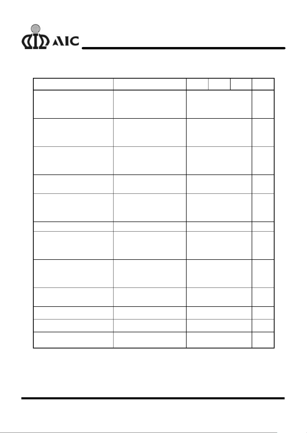
ELECTRICAL CHARACTERISTICS
n
specified)
PARAMETER TEST CONDITIONS MIN. TYP. MAX. UNIT
Reference Voltage AIC1117 (Adj.)
TJ=25°C
0°C≤TJ≤125°C
Output Voltage AIC1117-28, VIN=5V
AIC1117-33, VIN=5V
AIC1117-50, VIN=7V
2.65≤VIN≤7V
TJ=25°C 0.015 0.2Line Regulation
0°C≤TJ≤125°C 0.035 0.2
Load Regulation
Dropout Voltage
TJ=25°C, IO=10~800mA
0°C≤TJ≤125°C
∆V
, ∆V
OUT
10mA≤IO≤800mA
REF
(VIN=5V, TJ=25 °C, IO=10mA, Unless otherwise
1.238
1.225
2.82
3.26
4.95
=1%
1.25
1.25
2.85
3.30
5.00
0.1
0.2
1.2 1.4 V
1.262
1.275
2.88
3.33
5.05
0.3
0.4
V
V
%
%
0°C≤TJ≤125°C
Current Limit 0°C≤TJ≤125°C 0.85 A
2.65≤VIN≤7V
Adjusted Pin Current (I
Adjusted Pin Current Change
(∆I
)
ADJ
Temperature Stability
Minimum Load Current
RMS Output Noise (% of V
Ripple Rejection Ratio
ADJ
)
OUT
10mA≤IO≤ 800mA
0°C≤TJ≤125°C
2.65≤VIN≤7V
10mA≤IO≤800mA
0°C≤TJ≤125°C
IO=0.5A
0°C≤TJ≤125°C
0°C≤TJ≤125°C 5 10 mA
10Hz≤f≤10KHz 0.003 %
)
120Hz input ripple
C
=25µF
OUT
60 72 dB
55 120 µA
0.2 5 µA
0.5 %
3
 Loading...