

Page 1
DC
POWER SUPPLY
HANDBOOK
Application Note 90B
Page 2

TABLE OF CONTENTS
Introduction...........................................................................................................................................................6
Definitions ..............................................................................................................................................................6
Ambient Temperature..........................................................................................................................................6
Automatic (Auto) Parallel Operation ..................................................................................................................6
Automatic (Auto) Series Operation.....................................................................................................................7
Automatic (Auto) Tracking Operation................................................................................................................8
Carryover Time....................................................................................................................................................8
Complementary Tracking....................................................................................................................................8
Compliance Voltage ............................................................................................................................................8
Constant Current Power Supply ..........................................................................................................................8
Constant Voltage Power Supply..........................................................................................................................9
Constant Voltage/Constant Current (CV/CC) Power Supply..............................................................................9
Constant Voltage/Current Limiting (CV/CL) Power Supply............................................................................10
Crowbar Circuit.................................................................................................................................................11
Current Foldback...............................................................................................................................................11
Drift....................................................................................................................................................................11
Efficiency...........................................................................................................................................................11
Electromagnetic Interference (EMI)..................................................................................................................11
Inrush Current....................................................................................................................................................11
Load Effect (Load Regulation)..........................................................................................................................12
Load Effect Transient Recovery Time ..............................................................................................................12
Off-Line Power Supply......................................................................................................................................12
Output Impedance of a Power Supply...............................................................................................................12
PARD (Ripple and Noise).................................................................................................................................13
Programming Speed...........................................................................................................................................14
Remote Programming (Remote Control)...........................................................................................................14
Remote Sensing (Remote Error Sensing)..........................................................................................................15
Resolution..........................................................................................................................................................15
Source Effect (Line Regulation)........................................................................................................................15
Stability (see Drift)............................................................................................................................................16
Temperature Coefficient....................................................................................................................................16
Warm Up Time..................................................................................................................................................16
Principles of Operation.......................................................................................................................................17
Constant Voltage Power Supply........................................................................................................................17
Regulating Techniques...................................................................................................................................18
Series Regulation ...........................................................................................................................................18
Typical Series Regulated Power Supply........................................................................................................19
Pros and Cons of Series Regulated Supplies .................................................................................................19
The Series Regulated Supply - An Operational Amplifier............................................................................20
Series Regulator with Preregulator................................................................................................................23
Switching Regulation.....................................................................................................................................25
Basic Switching Supply.................................................................................................................................26
3
Page 3

Typical Switching Regulated Power Supplies...............................................................................................27
Summary of Basic Switching Regulator Configurations...............................................................................30
SCR Regulation..............................................................................................................................................31
Constant Current Power Supply ........................................................................................................................32
Constant Voltage/Constant Current (CV/CC) Power Supply............................................................................34
Constant Voltage/Current Limiting Supplies....................................................................................................36
Current Limit..................................................................................................................................................36
Current Foldback............................................................................................................................................37
Protection Circuits.............................................................................................................................................38
Protection Circuits for Linear Type Supplies ................................................................................................38
Overvoltage Crowbar Circuit Details ............................................................................................................39
Crowbar Response Time................................................................................................................................41
Special Purpose Power Supplies........................................................................................................................43
High Voltage Power Supply...........................................................................................................................43
High Performance Power Supplies................................................................................................................45
Extended Range Power Supplies ...................................................................................................................50
Advantages of Extended Range.....................................................................................................................50
Example of Extended Range Power Supply..................................................................................................51
Faster Down-Programming Speed .................................................................................................................53
Bipolar Power Supply/Amplifier...................................................................................................................54
Digitally Controlled Power Sources ..............................................................................................................55
AC and Load Connections..................................................................................................................................59
Checklist For AC and Load Connections..........................................................................................................59
AC Power Input Connections.........................................................................................................................59
Load Connections for One Power Supply......................................................................................................59
Load Connections for Two or More Power Supplies ....................................................................................60
AC Power Input Connections............................................................................................................................60
Autotransformers ...........................................................................................................................................61
Line Regulators..............................................................................................................................................61
Input AC Wire Rating....................................................................................................................................61
LOAD CONNECTIONS FOR ONE POWER SUPPLY...................................................................................61
DC Distribution Terminals.............................................................................................................................62
Load Decoupling............................................................................................................................................64
Ground Loops.................................................................................................................................................65
DC Common ..................................................................................................................................................68
DC Ground Point............................................................................................................................................72
Remote Error Sensing (Constant Voltage Operation Only)...........................................................................72
Load Connections For Two or More Power Supplies.......................................................................................78
DC Distribution Terminals.............................................................................................................................78
DC Common ..................................................................................................................................................79
DC Ground Point............................................................................................................................................79
Remote Programming.........................................................................................................................................80
Constant Voltage Remote Programming With Resistance Control...................................................................80
Remote Programming Connections ...............................................................................................................81
Output Drift....................................................................................................................................................81
Protecting Against Momentary Programming Errors....................................................................................82
Backup Protection for Open Programming Source........................................................................................83
4
Page 4

Constant Voltage Remote Programming With Voltage Control.......................................................................84
Programming with Unity Voltage Gain.........................................................................................................84
Programming with Variable Voltage Gain....................................................................................................85
Constant Current Remote Programming............................................................................................................86
Remote Programming Accuracy........................................................................................................................86
Remote Programming Speed .............................................................................................................................88
Output Voltage and Current Ratings................................................................................................................91
Duty Cycle Loading...........................................................................................................................................91
Reverse Current Loading...................................................................................................................................93
Dual Output Using Resistive Divider................................................................................................................94
Parallel Operation..............................................................................................................................................96
Auto Parallel Operation.....................................................................................................................................96
Series Operation ................................................................................................................................................97
Auto-Series Operation.......................................................................................................................................97
Auto Tracking Operation...................................................................................................................................99
Converting a Constant Voltage Power Supply To Constant Current Output....................................................99
PERFORMANCE MEASUREMENTS ..........................................................................................................101
Constant Voltage Power Supply Measurements..............................................................................................101
Precautions...................................................................................................................................................101
CV Source Effect (Line Regulation)............................................................................................................104
CV Load Effect (Load Regulation)..............................................................................................................104
CV PARD (Ripple and Noise).....................................................................................................................105
CV Load Effect Transient Recovery Time (Load Transient Recovery)......................................................109
CV Drift (Stability)......................................................................................................................................111
CV Temperature Coefficient........................................................................................................................111
CV Programming Speed...............................................................................................................................111
CV Output Impedance..................................................................................................................................113
Constant Current Power Supply Measurements..............................................................................................113
Precautions...................................................................................................................................................114
CC Source Effect (Line Regulation)............................................................................................................116
CC Load Effect (Load Regulation)..............................................................................................................116
CC PARD (Ripple and Noise) .....................................................................................................................116
CC Load Effect Transient Recovery Time ..................................................................................................117
CC Drift (Stability)......................................................................................................................................117
CC Temperature Coefficient........................................................................................................................119
Other Constant Current Specifications ........................................................................................................119
Index...................................................................................................................................................................120
5
Page 5

INTRODUCTION
Regulated power supplies employ engineering techniques drawn from the latest advances in many disciplines
such as: low-level, high-power, and wideband amplification techniques; operational amplifier and feedback
principles; pulse circuit techniques; and the constantly expanding frontiers of solid state component
development.
The full benefits of the engineering that has gone into the modern regulated power supply cannot be realized
unless the user first recognizes the inherent versatility and high performance capabilities, and second,
understands how to apply these features. This handbook is designed to aid that understanding by providing
complete information on the operation, performance, and connection of regulated power supplies.
The handbook is divided into six main sections: Definitions, Principles of Operation, AC and Load
Connections, Remote Programming, Output Voltage and Current Ratings, and Performance Measurements.
Each section contains answers to many of the questions commonly asked by users, like:
What is meant by auto-parallel operation?
What are the advantages and disadvantages of switching regulated supplies?
When should remote sensing at the load be used?
How can ground loops in multiple loads be avoided?
What factors affect programming speed?
What are the techniques for measuring power supply performance?
In summary, this is a book written not for the theorist, but for the user attempting to solve both traditional and
unusual application problems with regulated power supplies.
DEFINITIONS
AMBIENT TEMPERATURE
The temperature of the air immediately surrounding the power supply.
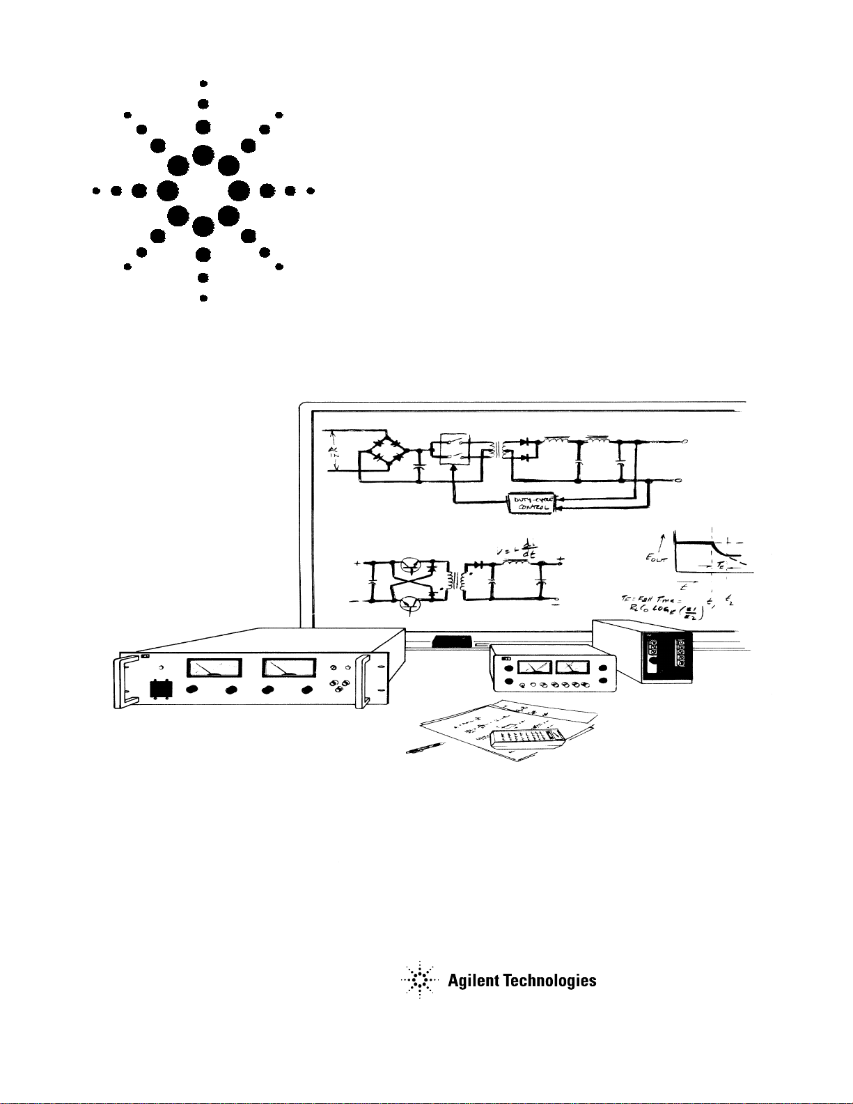
AUTOMATIC (AUTO) PARALLEL OPERATION
A master-slave parallel connection of the outputs of two or more supplies used for obtaining a current output
greater than that obtainable from one supply. Auto-Parallel operation is characterized by one-knob control,
equal current sharing, and no internal wiring changes. Normally only supplies having the same model number
may be connected in Auto-Parallel, since the units must have the same IR drop across the current monitoring
resistors at full current rating.
6
Page 6
AUTO-PARALLEL POWER SUPPLY SYSTEM
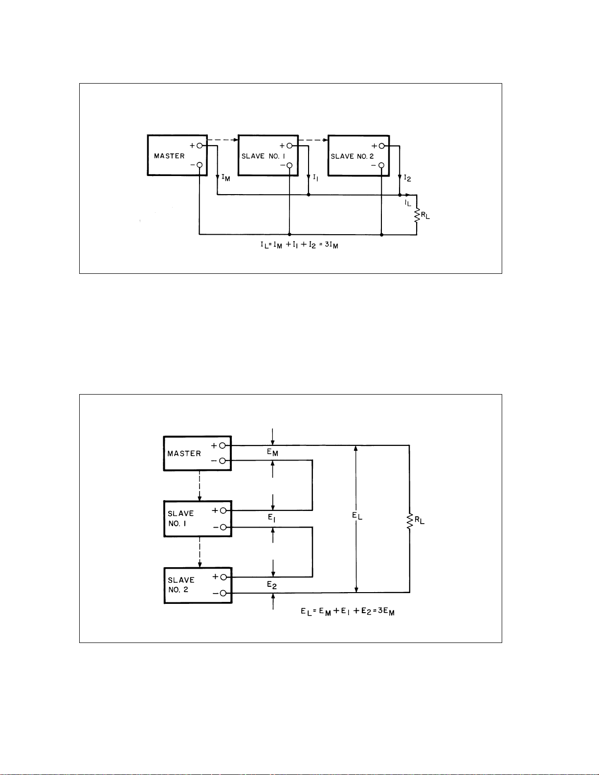
AUTOMATIC (AUTO) SERIES OPERATION
A master-slave series connection of the outputs of two or more power supplies used for obtaining a voltage
greater than that obtainable from one supply. Auto-Series operation, which is permissible up to 300 volts off
ground, is characterized by one-knob control, equal or proportional voltage sharing, and no internal wiring
changes. Different model numbers may be connected in Auto-Series without restriction, provided that each
slave is capable of Auto-Series operation.
AUTO-SERIES POWER SUPPLY SYSTEM
7
Page 7
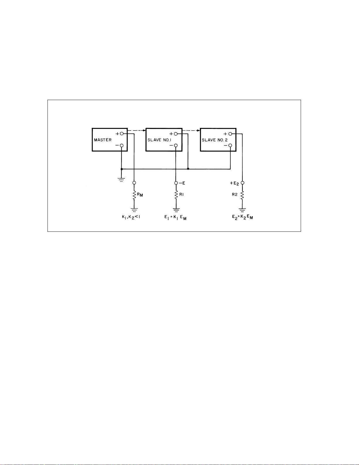
AUTOMATIC (AUTO) TRACKING OPERATION
A master-slave connection of two or more power supplies each of which has one of its output terminals in
common with one of the output terminals of all of the other power supplies. Auto-Tracking operation is
characterized by one-knob control, proportional output voltage from all supplies, and no internal wiring
changes. Useful where simultaneous turn-up, turn-down or proportional control of all power supplies in a
system is required.
AUTO-TRACKING POWER SUPPLY SYSTEM
CARRYOVER TIME
The period of time that a power supply's output will remain within specifications after loss of ac input power. It
is sometimes called holding time.
COMPLEMENTARY TRACKING
A master-slave interconnection similar to Auto-Tracking except that only two supplies are used and the output
voltage of the slave is always of opposite polarity with respect to the master. The amplitude of the slaves' output
voltage is equal to, or proportional to, that of the master. A pair of complementary tracking supplies is often
housed in a single unit.
COMPLIANCE VOLTAGE
The output voltage rating of a power supply operating in the constant current mode (analogous to the output
current rating of a supply operating in the constant voltage mode).
CONSTANT CURRENT POWER SUPPLY
A regulated power supply that acts to maintain its output current constant in spite of changes in load, line,
temperature, etc. Thus, for a change in load resistance, the output current remains constant while the output
voltage changes by whatever amount necessary to accomplish this.
8
Page 8
CONSTANT CURRENT POWER SUPPLY
OUTPUT CHARACTERISTICS
CONSTANT VOLTAGE POWER SUPPLY
A regulated power supply that acts to maintain its output voltage constant in spite of changes in load, line,
temperature, etc. Thus, for a change in load resistance, the output voltage of this type of supply remains
constant while the output current changes by whatever amount necessary to accomplish this.
CONSTANT VOLTAGE POWER SUPPLY
OUTPUT CHARACTERISTIC
CONSTANT VOLTAGE/CONSTANT CURRENT (CV/CC) POWER SUPPLY
A power supply that acts as a constant voltage source for comparatively large values of load resistance and as a
constant current source for comparatively small values of load resistance. The automatic crossover or transition
between these two modes of operation occurs at a "critical" or "crossover" value of load resistance Rc = Es/Is,
where Es is the front panel voltage control setting and Is is the front panel current control setting.
9
Page 9
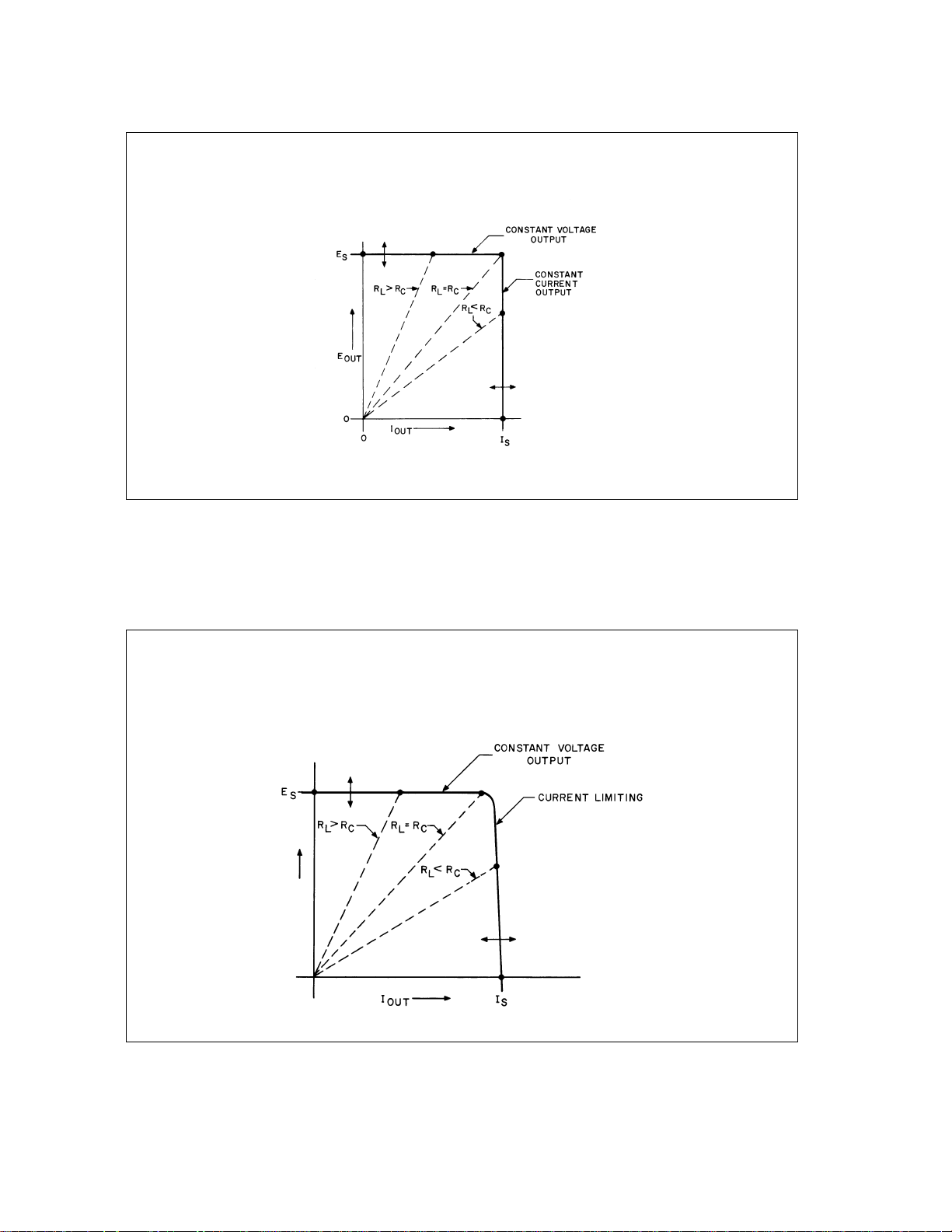
CONSTANT VOLTAGE/CONSTANT CURRENT
(CV/CC) OUTPUT CHARACTERISTIC
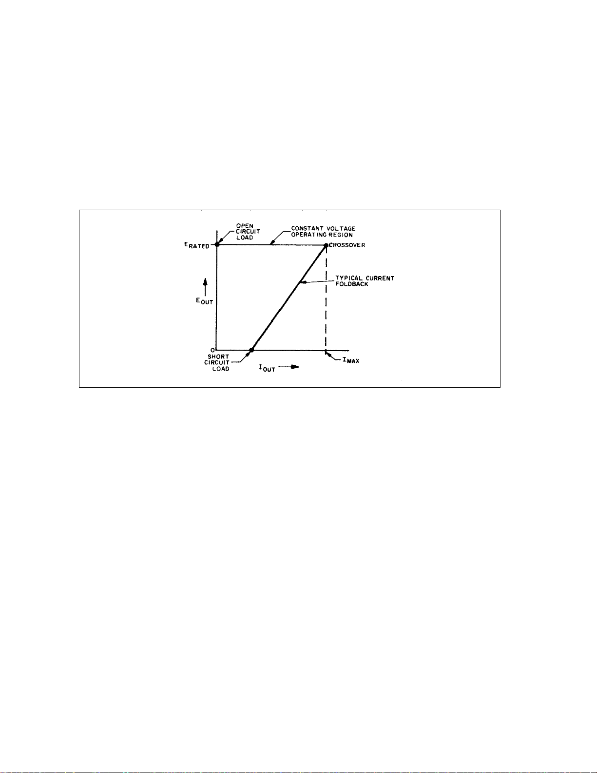
CONSTANT VOLTAGE/CURRENT LIMITING (CV/CL) POWER SUPPLY
A supply similar to a CV/CC supply except for less precise regulation at low values of load resistance, i.e., in
the current limiting region of operation. One form of current limiting is shown above.
CONSTANT VOLTAGE/ CURRENT LIMITING
(CV/CL) OUTPUT CHARACTERISTIC
10
Page 10
CROWBAR CIRCUIT
An overvoltage protection circuit that monitors the output voltage of the supply and rapidly places a short
circuit (or crowbar) across the output terminals if a preset voltage level is exceeded.
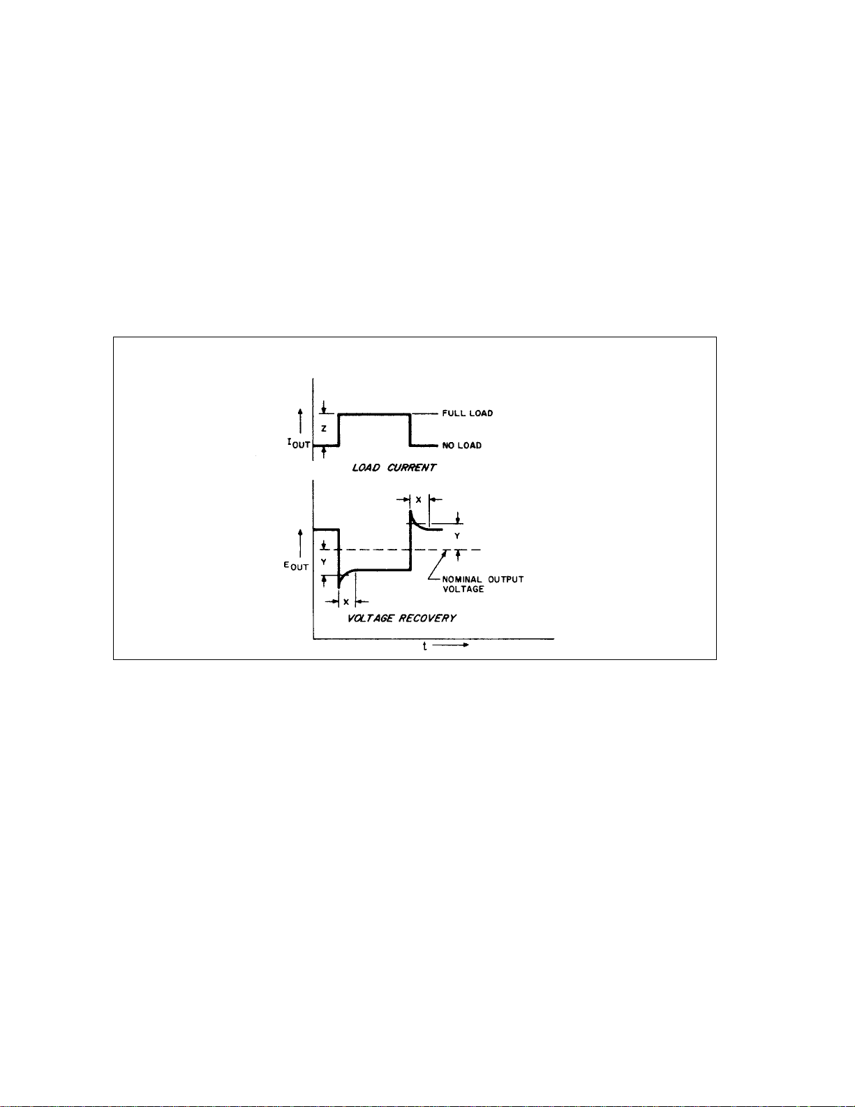
CURRENT FOLDBACK
Another form of current limiting often used in fixed output voltage supplies. For load resistance smaller than
the crossover value, the current, as well as the voltage, decreases along a foldback locus.
DRIFT
The maximum change in power supply output during a stated period of time (usually 8 hours) following a
warm-up period, with all influence and control quantities (such as; load, ac line, and ambient temperature)
maintained constant. Drift includes periodic and random deviations (PARD) over a bandwidth from dc to 20Hz.
(At frequencies above 20Hz, PARD is specified separately.)
EFFICIENCY
Expressed in percent, efficiency is the total output power of the supply divided by the active input power.
Unless otherwise specified, Agilent measures efficiency at maximum rated output power and at worst case
conditions of the ac line voltage.
ELECTROMAGNETIC INTERFERENCE (EMI)
Any type of electromagnetic energy that could degrade the performance of electrical or electronic equipment.
The EMI generated by a power supply can be propagated either by conduction (via the input and output leads)
or by radiation from the units' case. The terms "noise" and "radio-frequency interference" (RFI) are sometimes
used in the same context.
INRUSH CURRENT
The maximum instantaneous value of the input current to a power supply when ac power is first applied.
11
Page 11
LOAD EFFECT (LOAD REGULATION)
Formerly known as load regulation, load effect is the change in the steady-state value of the dc output voltage
or current resulting from a specified change in the load current (of a constant-voltage supply) or the load
voltage (of a constant-current supply), with all other influence quantities maintained constant.
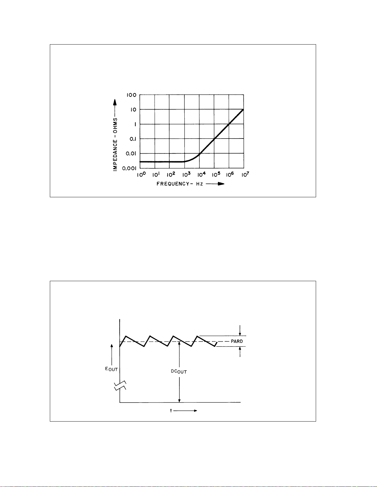
LOAD EFFECT TRANSIENT RECOVERY TIME
Sometimes referred to as transient recovery time or transient response time, it is, loosely speaking, the time
required for the output voltage of a power supply to return to within a level approximating the normal dc output
following a sudden change in load current. More exactly, Load Transient Recovery Time for a CV supply is the
time "X" required for the output voltage to recover to, and stay within "Y" millivolts of the nominal output
voltage following a "Z" amp step change in load current --where:
TRANSIENT REC OVERY TIME
(1) "Y" is specified separately for each model but is generally of the same order as the load regulation
specification.
(2) The nominal output voltage is defined as the dc level halfway between the steady state output voltage
before and after the imposed load change.
(3) "Z" is the specified load current change, typically equal to the full load current rating of the
OFF-LINE POWER SUPPLY
A power supply whose input rectifier circuits operate directly from the ac power line, without transformer
isolation.
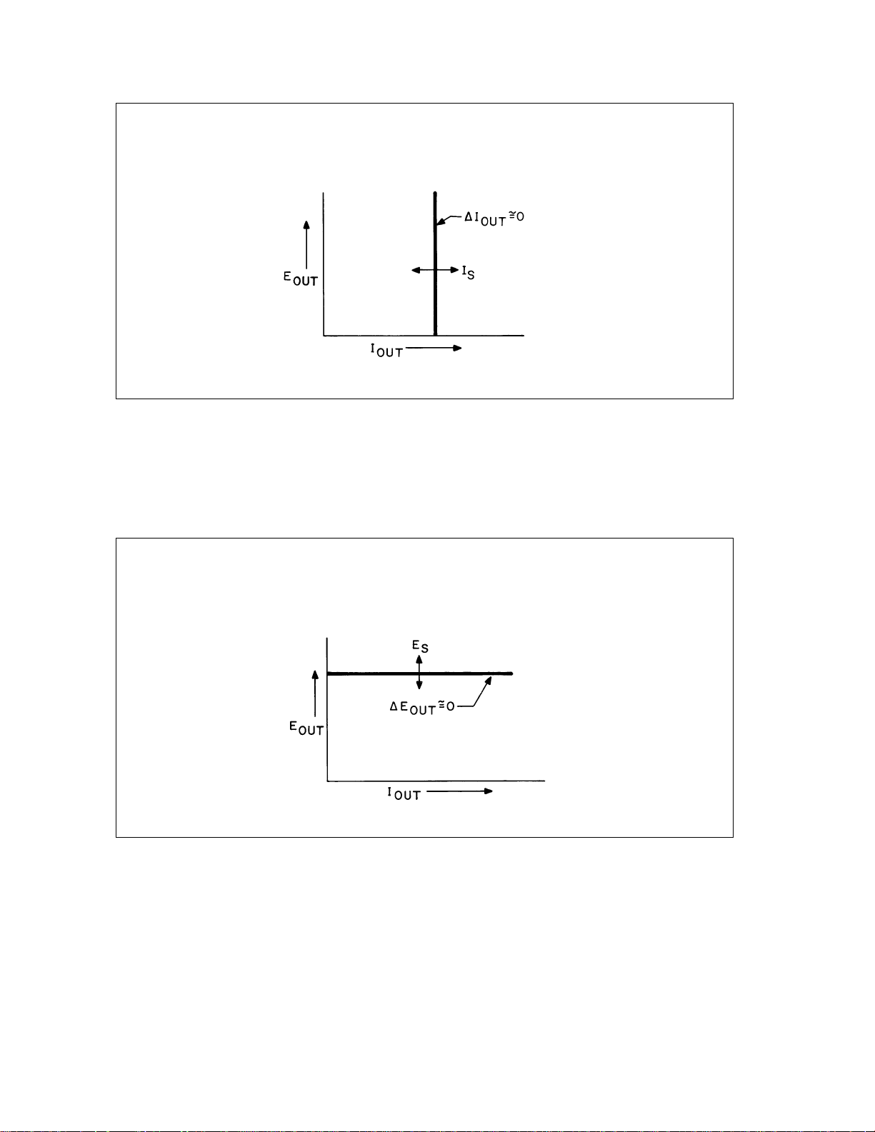
OUTPUT IMPEDANCE OF A POWER SUPPLY
At any frequency of load change, ∆EOUT/∆IOUT. Strictly speaking, the definition applies only for a sinusoidal
load disturbance, unless the measurement is made at zero frequency (dc). The output impedance of an ideal
constant voltage power supply would be zero at all frequencies, while the output impedance for an ideal
constant current power supply would be infinite at all frequencies.
12
Page 12
TYPICAL OUTPUT IMPEDANCE OF A CONSTANT
VOLTAGE POWER SUPPLY
PARD (RIPPLE AND NOISE)
The term PARD is an acronym for "Periodic and Random deviation" and replaces the former term ripple and
noise. PARD is the residual ac component that is superimposed on the dc output voltage or current of a power
supply. It is measured over a specified bandwidth, with all influence and control quantities maintained constant.
PARD is specified in rms and/or peak-to-peak values over a bandwidth of 20Hz to 20MHz. Fluctuations below
20Hz are treated as drift. Attempting to measure PARD with an instrument that has insufficient bandwidth may
conceal high frequency spikes that could be detrimental to a load.
DC OUTPUT OF POWER SUPPLY AND
SUPERIMPOSED PARD COMPONENT
13
Page 13
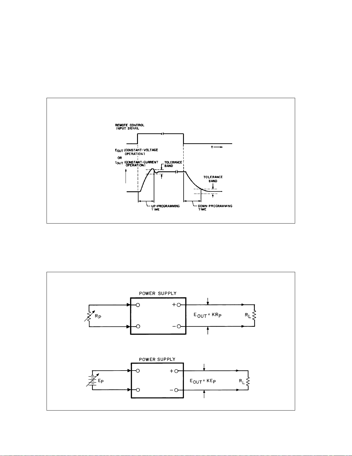
PROGRAMMING SPEED
The maximum time required for the output voltage or current to change from an initial value to within a
tolerance band of the newly programmed value following the onset of a step change in the programming input
signal. Because the programming speed depends on the loading of the supply and on whether the output is being
programmed to a higher or lower value, programming speed is usually specified at no load and full load and in
both the up and down directions.
PROGRAMMING SPEED WAVEFORMS
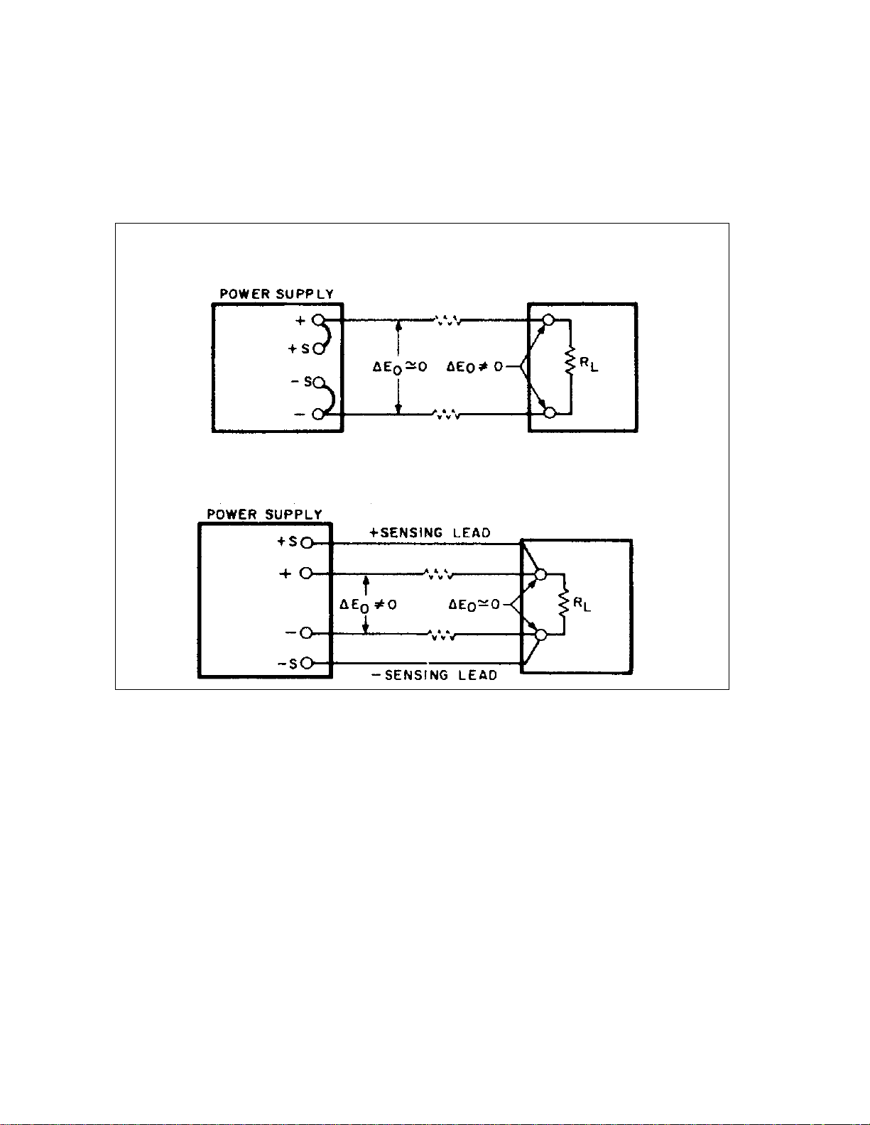
REMOTE PROGRAMMING (REMOTE CONTROL)
Control of the regulated output voltage or current of a power supply by means of a remotely varied resistance or
voltage. The illustrations below show examples of constant voltage remote programming. CC applications are
similar.
REMOTE PROGRAMMING USING RESISTANCE CONTROL
REMOTE PROGRAMMING USING VOLTAGE CONTROL
14
Page 14
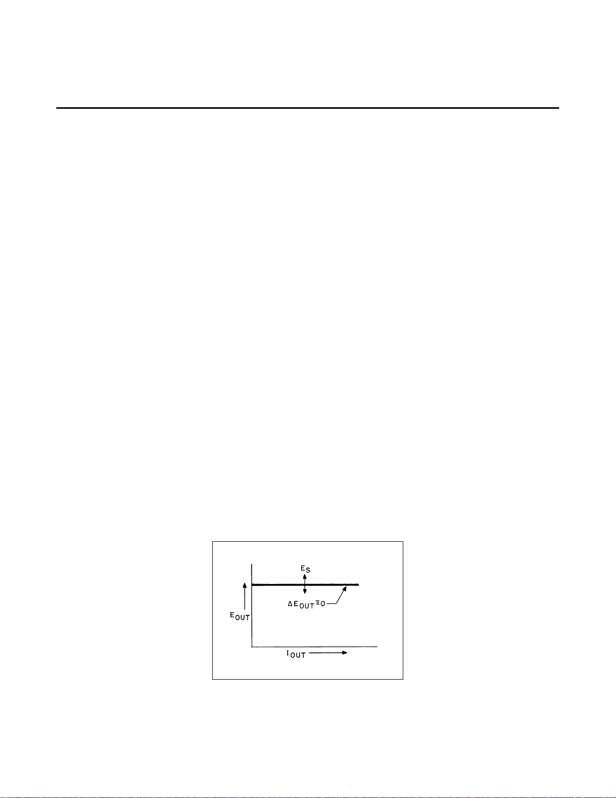
REMOTE SENSING (REMOTE ERROR SENSING)
A means whereby a constant voltage power supply monitors and regulates its output voltage directly at the load
terminals (instead of the power supply output terminals). Two low current sensing leads are connected between
the load terminals and special sensing terminals located on the power supply, permitting the power supply
output voltage to compensate for IR drops in the load leads (up to a specified limit).
POWER SUPPLY AND LOAD CONNECTED NORMALLY
POWER SUPPLY AND LOAD CONNECTED FOR REMOTE SENSING
RESOLUTION
The smallest change in output voltage or current that can be obtained using the front panel controls.
SOURCE EFFECT (LINE REGULATION)
Formerly known as line regulation, source effect is the change in the steady-state value of the dc output voltage
(of a CV supply) or current (of a CC supply) due to a specified change in the source (ac line) voltage, with all
other influence quantities maintained constant. Source effect is usually measured after a "complete" change in
the ac line voltage; from low line to high line or vice-versa.
15
Page 15

STABILITY (SEE DRIFT)
TEMPERATURE COEFFICIENT
For a power supply operated at constant load and constant ac input, the maximum steady-state change in output
voltage (for a constant voltage supply) or output current (for a constant current supply) for each degree change
in the ambient temperature, with all other influence quantities maintained constant.
WARM UP TIME
The time interval required by a power supply to meet all performance specifications after it is first turned on.
16
Page 16
PRINCIPLES OF OPERATION
Electronic power supplies are defined as circuits which transform electrical input power--either ac or dc--into
output power--either ac or dc. This definition thus excludes power supplies based on rotating machine
principles and distinguishes power supplies from the more general category of electrical power sources which
derive electrical power from other energy forms (e. g., batteries, solar cells, fuel cells).
Electronic power supplies can be divided into four broad classifications:
(1) ac in, ac out-line regulators and frequency changers
(2) dc in, dc out-converters and dc regulators
(3) dc in, ac out-inverters
(4) ac in, dc out
This last category is by far the most common of the four and is generally the one referred to when speaking of a
"power supply". Most of this Handbook is devoted to ac in/dc out power supplies, although a brief description
of a dc-to-dc converter is presented later in this section.
Four basic outputs or modes or operation can be provided by dc output power supplies:
• Constant Voltage: The output voltage is maintained constant in spite of changes in load, line, or
temperature.
• Constant Current: The output current is maintained constant in spite of changes in load, line, or
temperature.
• Voltage Limit: Same as Constant Voltage except for less precise regulation characteristics.
• Current Limit: Similar to Constant Current except for less precise regulation.
As explained in this section, power supplies are designed to offer these outputs in various combinations for
different applications.
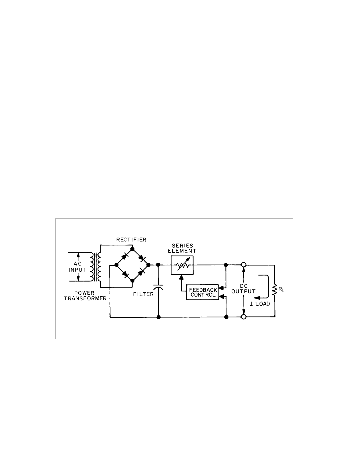
CONSTANT VOLTAGE POWER SUPPLY
An ideal constant voltage power supply would have zero output impedance at all frequencies. Thus, as shown in
Figure 1, the voltage would remain perfectly constant in spite of any changes in output current demanded by the
load.
Figure 1. Ideal Constant Voltage Power Supply Output Characteristic
17
Page 17
A simple unregulated power supply consisting of only a rectifier and filter is not capable of providing a ripple
free dc output voltage whose value remains reasonably constant. To obtain even a coarse approximation of the
ideal output characteristic of Figure 1, some type of control element (regulator) must be included in the supply.
Regulating Techniques
Most of today's constant voltage power supplies employ one of these four regulating techniques:
a. Series (Linear)
b. Preregulator/Series Regulator
c. Switching
d. SCR
Series Regulation
Series regulated power supplies were introduced many years ago and are still used extensively today. They have
survived the transition from vacuum tubes to transistors, and modern supplies often utilize IC's, the latest in
power semiconductors, and some sophisticated control and protection circuitry.
The basic design technique, which has not changed over the years, consists of placing a control element in
series with the rectifier and load device. Figure 2 shows a simplified schematic of a series regulated supply with
the series element depicted as a variable resistor. Feedback control circuits continuously monitor the output and
adjust the series "resistance" to maintain a constant output voltage. Because the variable resistance of Figure 2
is actually one or more power transistors operating in the linear (class A) mode, supplies with this type of
regulator are often called linear power supplies.
Figure 2. Basic Series Regulated Supply
Notice that the variable resistance element can also be connected in parallel with the load to form a shunt
regulator. However, this type of regulator is seldom used because it must withstand full output voltage under
normal operating conditions, making it less efficient for most applications.
18
Page 18
Typical Series Regulated Power Supply
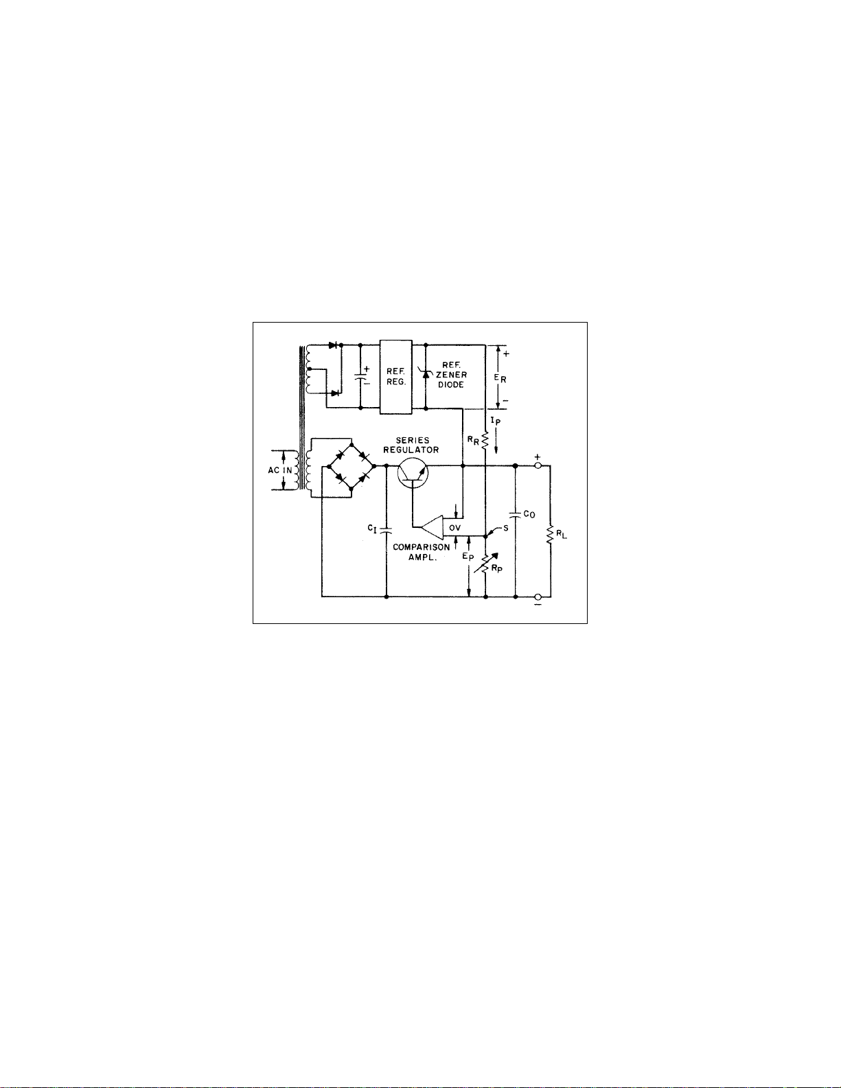
Figure 3 shows the basic feedback circuit principle used in Agilent series regulated power supplies. The ac
input, after passing through a power transformer, is rectified and filtered. By feedback action, the series
regulator alters its voltage drop to keep the regulated dc output voltage constant despite variations in the ac line,
the load, or the ambient temperature.
The comparison amplifier continuously monitors the difference between the voltage across the voltage control
resistor, RP, and the output voltage. If these voltages are not equal, the comparison amplifier produces an
amplified difference (error) signal. This signal is of the magnitude and polarity necessary to change the
conduction of the series regulator which, in turn, changes the current through the load resistor until the output
voltage equals the voltage (EP) across the voltage control.
Figure 3. Series Regulated Constant Voltage Power Supply
Since the net difference between the two voltage inputs to the comparison amplifier is kept at zero by feedback
action, the voltage across resistor R
current I
flowing through RR is constant and equal to ER/RR. The input impedance of the comparison amplifier
P
is very high, so essentially all of the current I
programming current I
is constant, EP (and hence the output voltage) is variable and directly proportional to RP.
P
Thus, the output voltage becomes zero if R
is also held equal to the reference voltage ER. Thus the programming
R
flowing through RR also flows through RP. Because this
P
is reduced to zero ohms.
P
Of course, not all series regulated supplies are continuously adjustable down to zero volts. Those of the OEM
modular type are used in system applications and, thus, their output voltage adjustment is restricted to a narrow
range or slot. However, operation of these supplies is virtually identical to that just described.
Pros and Cons of Series Regulated Supplies
Series regulated supplies have many advantages and usually provide the simplest most effective means of
satisfying high performance and low power requirements.
In terms of performance, series regulated supplies have very precise regulation properties and respond quickly
19
Page 19
to variations of the line and load. Hence, their line and load regulation and transient recovery time* are superior
to supplies using any of the other regulation techniques. These supplies also exhibit the lowest ripple and noise,
are tolerant of ambient temperature changes, and with their circuit simplicity, have a high reliability.
*Power supply performance specifications are described in the Definitions section of this handbook.
The major drawback of the series regulated supply is its relatively low efficiency. This is caused mainly by the
series transistor which, operating in the linear mode, continuously dissipates power in carrying out its
regulation function. Efficiency (defined as the percentage of a supply's input power that it can deliver as useful
output: P
OUT/PIN
), ranges typically between 30 and 45% for series regulated supplies. With the present need for
energy conservation, this inefficiency is being scrutinized very closely.
For many of today's applications, the size and weight of linear supplies constitute another disadvantage. The
power transformer, inductors, and filter capacitors necessary for operation at the 60Hz line frequency tend to be
large and heavy, and the heat sink required for the inherently dissipative series regulator increases the overall
size.
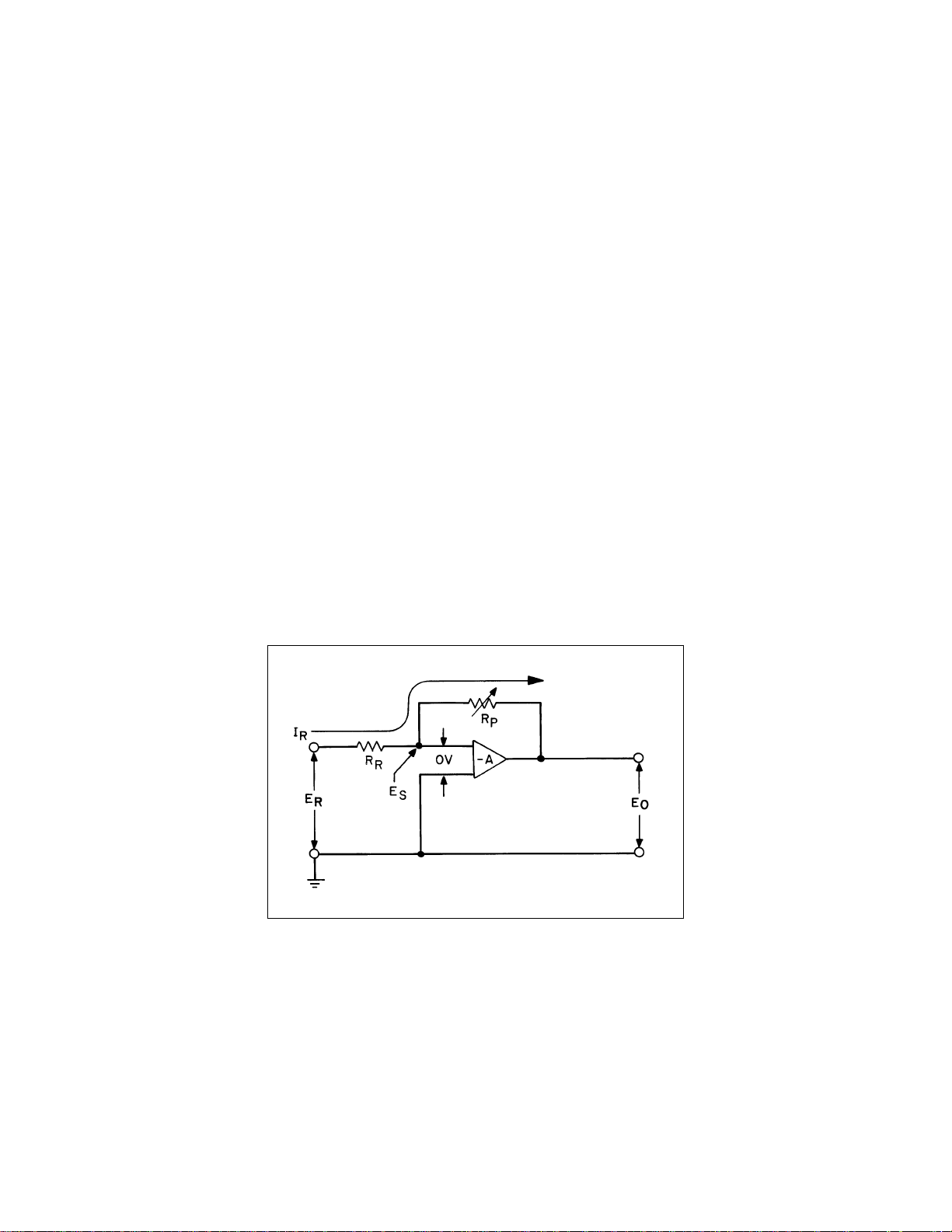
The Series Regulated Supply - An Operational Amplifier
The following analogy views the series regulated power supply as an operational amplifier. Considering the
power supply as an operational amplifier can often give the user a quick insight into power supply behavior and
help in evaluating a power supply for a specific application.
An operational amplifier (Figure 4) is a high gain dc amplifier that employs negative feedback. The power
supply, like an operational amplifier, is also a high gain dc amplifier in which degenerative feedback is
arranged so the operational gain is the ratio of two resistors.
Figure 4. Operational Amplifier
As shown in Figure 4, the input voltage E
voltage is fed back to this same summing point through resistor R
input current to the amplifier can be considered negligibly small, and all of the input current I
both resistors R
and RP. As a result:
R
is connected to the summing point via resistor RR, and the output
R
. Since the input impedance is very high, the
P
flows through
R
20
Page 20

IR =
ER-E
R
S
R
=
ES-E
R
O
P
Then multiplying both sides by RRRP, we obtain
E
= ESRP + ESRR –EORR.(2)
RRP
Figure 4 yields a second equation relating the amplifier output to its gain and voltage input
E
=ES (-A) (3)
O
which when substituted in equation (2) and solved for Es yields
E
R RP
ES =
+ RR (1+A)
R
P
Normally, the operational amplifier gain is very high, commonly 10,000 or more. In equation (4)
If we let A → ∞
Then Es→ O
(1)
(4)
(5)
This important result enables us to say that the two input voltages of the comparison amplifier of Figure 4 (and
Figure 3) are held equal by feedback action.
In modern well-regulated power supplies, the summing point voltage Es is at most a few millivolts. Substituting
Es = 0 into equation (1) yields the standard gain expression for the operational amplifier
R
P
EO = -E
R
R
R
(6)
Notice that from equation 6 and Figure 4, doubling the value of RP doubles the output voltage.
To convert the operational amplifier of Figure 4 into a power supply we must first apply as its input a fixed dc
input reference voltage E
(see Figure 5).
R
21
Page 21
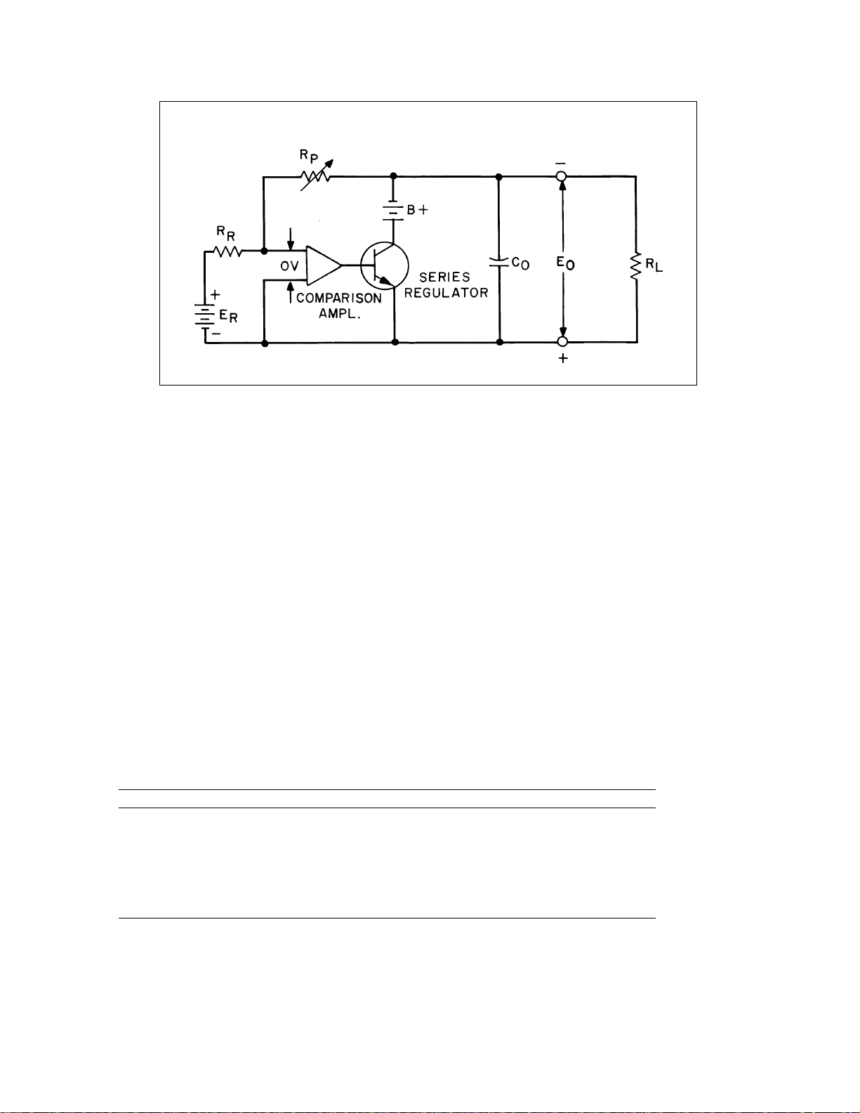
Figure 5. Operational Amplifier w i t h DC I nput Signal
A large electrolytic capacitor is then added across the output terminals of the operational amplifier. The
impedance of this capacitor in the middle range of frequencies (where the overall gain of the amplifier falls off
and becomes less than unity) is much lower than the impedance of any load that might normally be connected to
the amplifier output. Thus, the phase shift through the output terminals is independent of the phase angle of the
load applied and depends only on the impedance of the output capacitor at medium and high frequencies.
Hence, amplifier feedback stability is assured and no oscillation will occur regardless of the type of load
imposed.
In addition, the output stage inside the amplifier block in Figure 4 is removed and shown separately. After these
changes have been carried out, the modified operational amplifier of Figure 5 results.
Replacing the batteries of Figure 5 with rectifiers and a reference zener diode results in the circuit of Figure 6.
A point by point comparison of Figures 3 and 6 reveals that they have identical topology--all connections are
the same, only the position of the components on the diagram differs!
Thus, a series regulated power supply is an operational amplifier. The input signal to this operational amplifier
is the reference voltage. The output signal is regulated dc. The following chart summarizes the corresponding
terms used for an operational amplifier and a power supply.
Operational Amplifier Constant Voltage Power Supply
Input Signal Reference Voltage
Output Signal Regulated DC
Amplifier Regulator
Output Stage Series Regulating Transistor
Bias Power Supply Rectifier/Filter
Gain Control Output Voltage Control
As a result of the specific method used in transforming an operational amplifier into a power supply, some
restrictions are placed on the general behavior of the power supply. The most important of these are:
(1) The large output capacitor Co limits the bandwidth. *
22
Page 22
(2) The use of a fixed dc input voltage means that the output voltage can only be one polarity, the opposite of
the reference polarity.**
(3) The series regulator can conduct current in only one direction. This, together with the fact that the rectifier
has a given polarity, means that the power supply can only deliver current to the load, and cannot absorb
current from the load.
* Special design steps have been added to the design of most Agilent low voltage supplies to permit a
significant reduction in the size of the output capacitor merely by changing straps on the rear terminal strip (see
page 89).
** In Agilent’s line of Bipolar Power Supply/Amplifiers this output capacitor is virtually eliminated by using a
special feedback design. In addition, BPS/A instruments are capable of ac output, conduct current in either
direction, and their outputs are continuously variable through zero (see page 54).
Figure 6. Operational Amplifier Representation of Adjustable CV Power Suppl y
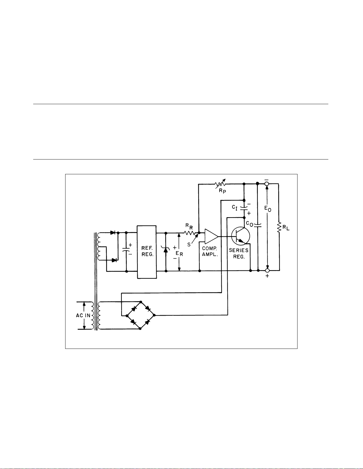
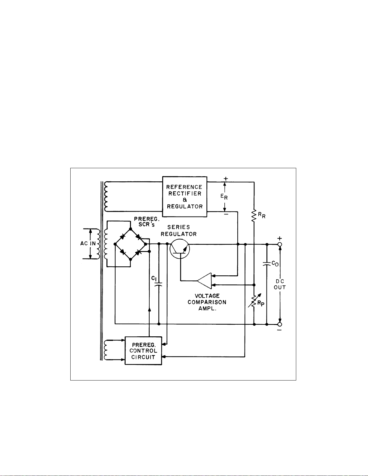
Series Regulator with Preregulator
Adding a preregulator ahead of the series regulator allows the circuit techniques already developed for low
power supplies to be extended readily to medium and higher power designs. The preregulator minimizes the
power dissipated in the series regulating elements by maintaining the voltage drop across the regulator at a low
and constant level. This improves efficiency by 10 to 20% while still retaining the excellent regulation and low
ripple and noise of a series regulated supply. In addition, fewer series regulating transistors are required, thus
23
Page 23
minimizing size increases.
Figure 7 shows an earlier Agilent power supply using SCR's as the preregulating elements. Silicon Controlled
Rectifiers, the semiconductor equivalent of thyratons, are rectifiers which remain in a non-conductive state,
even when forward voltage is provided from anode to cathode, until a positive trigger pulse is applied to a third
terminal (the gate). Then the SCR "fires", conducting current with a very low effective resistance; it remains
conducting after the trigger pulse has been removed until the forward anode voltage is removed or reversed. On
more recent preregulator designs, the SCR's are replaced by a single triac, which is a bidirectional device.
Whenever a gating pulse is received, the triac conducts current in a direction that is dependent on the polarity
of the voltage across it. Triacs are usually connected in series with one side of the input transformer primary,
while SCR's are included in two arms of the bridge rectifier as shown in Figure 7. No matter which type of
element is used, the basic operating principle of the preregulator circuit is the same. During each half cycle of
the input, the firing duration of the SCR's is controlled so that the bridge rectifier output varies in accordance
with the demands imposed by the dc output voltage and current of the supply.
Figure 7. Constant Voltage Power Supply with SCR Preregulator
The function of the preregulator control circuit is to compute the firing time of the SCR trigger pulse for each
24
Page 24
half cycle of input ac and hold the voltage drop across the series regulator constant in spite of changes in load
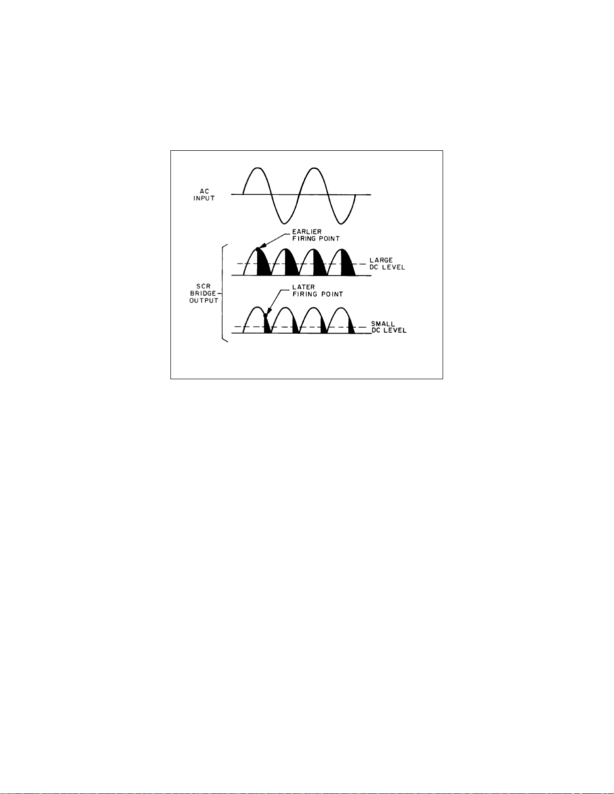
current, output voltage, or input line voltage. Figure 8 shows how varying the conduction angle of the SCR's
affects the amplitude of the output voltage and current delivered by the SCR bridge rectifier of Figure 7. An
earlier firing point results in a greater fraction of halfcycle power from the bridge and a higher dc level across
the input filter capacitance. For later firing times, the dc average is decreased.
Figure 8. SCR Conduction Angle Control of Preregulator Output
The reaction time of an Agilent preregulator control circuit is much faster than earlier SCR or magamp circuits.
Sudden changes in line voltage or load current result in a correction in the timing of the next SCR trigger pulse,
which can be no farther away than one half cycle (approximately 8 milliseconds for a 60Hz input). The large
filter capacitance across the rectifier output allows only a small voltage change to occur during any 8
millisecond interval, avoiding the risk of transient drop-out and loss of regulation due to sudden changes in load
or line. The final burden of providing precise and rapid output voltage regulation rests with the series regulator,
while the preregulator handles the coarser and slower regulation demands.
The preregulator SCRs, together with the leakage inductance of the power transformer, limit high inrush
currents during turn-on. A slow-start circuit allows gradual turn-on of the SCRs while the leakage inductance
acts as a small filter choke in series with the SCRs. Thus, both the supply's input components and other ac
connected instruments are protected from surge currents.
Switching Regulation
The rising cost of electricity and continuous reductions in the size of many electronic devices have stimulated
recent developments in switching regulated power supplies. These supplies are smaller, lighter, and dissipate
less power than equivalent series regulated or series/preregulated supplies.
Although basic switching regulator technology and its advantages have been known for years, a lack of the
necessary switching transistors, rectifier diodes, and filter capacitors caused certain performance problems that
were costly to minimize. As a result, these supplies were used only in airborne, space, or other applications
where cost was a secondary consideration to weight and size. However, the advent of high-voltage, fast
25
Page 25
switching power transistors, fast recovery diodes, and new filter capacitors with lower series resistance and
inductance, have propelled switching supplies to a position of great prominence in the power supply industry.
Presently, switching supplies still have a strong growth potential and are constantly changing as better
components become available and new design techniques emerge. Concurrently, performance is improving,
costs are dropping, and the power level at which switching supplies are competitive with linear supplies
continues to decrease. Before continuing with this discussion, a look at a basic switching supply circuit will
help to explain some of the reasons for its popularity.
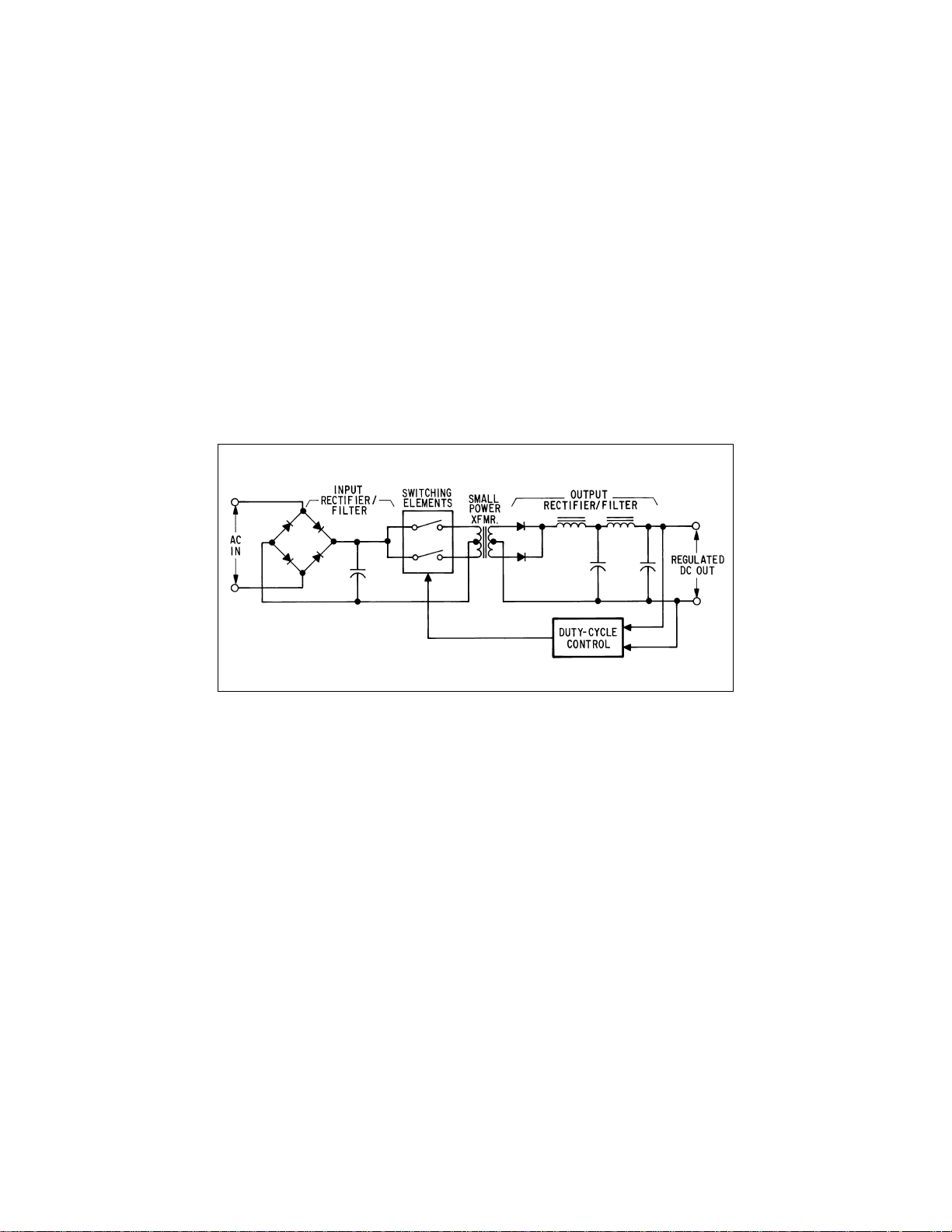
Basic Switching Supply
In a switching supply, the regulating elements consist of series connected transistors that act as rapidly opened
and closed switches (Figure 9). The input ac is first converted to unregulated dc which, in turn, is "chopped" by
the switching element operating at a rapid rate(typically 20KHz). The resultant 20KHz pulse train is
transformer-coupled to an output network which provides final rectification and smoothing of the dc output.
Regulation is accomplished by control circuits that vary the on-off periods (duty cycle) of the switching
elements if the output voltage attempts to chance.
Figure 9. Basic Swit chi ng Supply
Operating Advantages and Disadvantages. Because switching regulators are basically on/off devices, they
avoid the higher power dissipation associated with the rheostat-like action of a series regulator. The switching
transistors dissipate very little power when either saturated (on) or nonconducting (off) and most of the power
losses occur elsewhere in the supply. Efficiencies ranging from 65 to 85% are typical for switching supplies, as
compared to 30 to 45% efficiencies for linear types. With less wasted power, switching supplies run at cooler
temperatures, cost less to operate, and have smaller regulator heat sinks.
Significant size and weight reductions for switching supplies are achieved because of their high switching rate.
The power transformer, inductors, and filter capacitors for 20KHz operation are much smaller and lighter than
those required for operation at power line frequencies. Typically, a switching supply is less than one-third the
size and weight of a comparable series regulated supply.
Besides high efficiency and reduced size and weight, switching supplies have still another benefit that suits the
needs of the modern environment. That is their ability to operate under low ac input voltage (brownout) conditions and a relatively long carryover (or holdup) of their output if input power is lost momentarily. The
switching supply is superior to the linear supply in this regard because more energy can be stored in its input
filter capacitance. To provide the low voltage, high current output required in many of today's applications, the
series regulated supply first steps down the input ac and energy storage must be in a filter capacitor with a low
26
Page 26

voltage across it. In a switching supply, however, the input ac is rectified directly (Figure 9) and the filter
capacitor is allowed to charge to a much higher voltage (the peaks of the ac line). Since the energy stored in a
capacitor = 0.5CV2, while its volume (size) tends to be proportional to CV, storage capability is better in a
switching supply.
Although its advantages are impressive, a switching supply does have some inherent operating characteristics
that could limit its effectiveness in certain applications. One of these is that its transient recovery time (dynamic
load regulation) is slower than that of a series regulated supply. In a linear supply, recovery time is limited only
by the speeds of the semiconductors used in the series regulator and control circuitry. In a switching supply,
however, recovery is limited mainly by the inductance in the output filter. This may or may not be of
significance to the user, depending upon the specific application.
Also, electro-magntic interference (EMI) is a natural byproduct of the on-off switching within
these supplies. This interference can be conducted to the load (resulting in higher output ripple and
noise), it can be conducted back into the ac line, and it can be radiated into the surrounding
atmosphere. For this reason, all Agilent Technologies switching supplies have built-in shields and
filter networks that substantially reduce EMI and control output ripple and noise.
Reliability has been another area of concern with switching supplies. Higher circuit complexity
and the relative newness of switching regulator technology have in the past contributed to a
diminished confidence in switching supply reliability. Since their entry into this market, Agilent
has placed a strong emphasis on the reliability of their switching supplies. Field failures have been
minimized by such factors as careful component evaluation, MTBF life tests, factory "burn-in"
procedures, and sound design practices.
Typical Switching Regulated Power Supplies
Currently, switching supplies are widely used by Original Equipment Manufacturers (OEMs). This class of
switching supply provides a high degree of efficiency and compactness, moderate-to-good regulation and ripple
characteristics, and a semi-fixed constant voltage output.
Figure 10 shows one of Agilent’s higher power, yet less complex, OEM switching supplies. Regulation is
accomplished by a pair of push-pull switching transistors operating under control of a feedback network
consisting of a pulse width modulator and a voltage comparison amplifier. The feedback elements control the
ON periods of the switching transistors to adjust the duty cycle of the bipolar waveform (E) delivered to the
output rectifier/filter. Here the waveform is rectified and averaged to provide a dc output level that is
proportional to the duty cycle of the waveform. Hence, increasing the ON times of the switches increases the
output voltage and vice-versa.
The waveforms of Figure 10 provide a more detailed picture of circuit operation. The voltage comparison
amplifier continuously compares a fraction of the output voltage with a stable reference (EREF) to produce the
VCONTROL level for the turn-on comparator. This device compares the VCONTROL input with a triangular
ramp waveform (A) occurring at a fixed 40KHz rate. When the ramp voltage is more positive than the control
level, a turn-on signal (B) is generated. Notice that an increase or decrease in the VCONTROL voltage varies
the width of the output pulses at B and thus the ON time of the switches.
Steering logic within the modulator chip causes switching transistors Q1 and Q2 to turn on alternately, so that
each switch operates at one-half the ramp frequency (20KHz).
27
Page 27
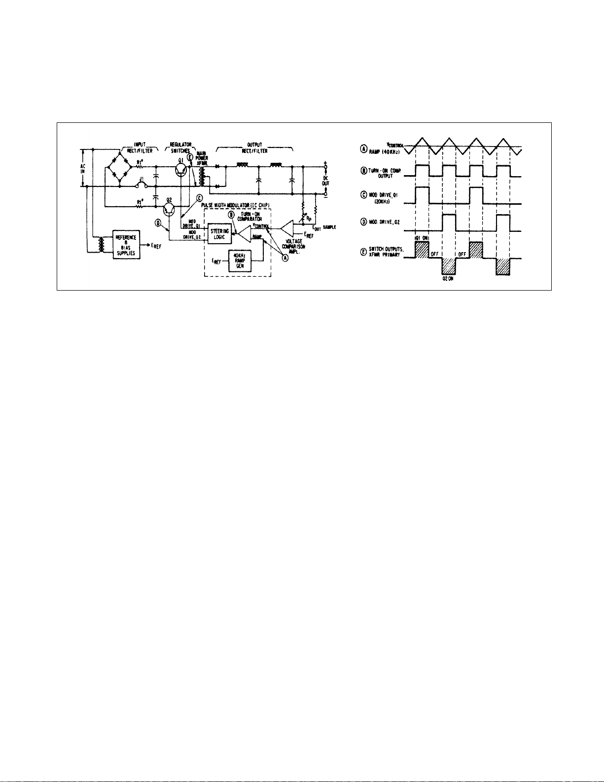
Included, but not shown, in the modulator chip are additional circuits that establish a minimum "dead time" (off
time) for the switching transistors. This ensures that both switching transistors cannot conduct simultaneously
during maximum duty cycle conditions.
Figure 10. Switchi ng Regul ated Constant Voltage Supply
Ac Inrush Current Protection. Because the input filter capacitors are connected directly across the rectified
line, some form of surge protection must be provided to limit line inrush currents at turn-on. If not controlled,
large inrush surges could trip circuit breakers, weld switch contacts, or affect the operation of other equipment
connected to the same ac line. Protection is provided by a pair of thermistors in the input rectifier circuit. With
their high negative temperature coefficient of resistance, the thermistors present a relatively high resistance
when cold (during the turn-on period), and a very low resistance after they heat up.
A shorting strap (J1) permits the configuration of the input rectifier-filter to be altered for different ac inputs.
For a 174-250Vac input, the strap is removed and the circuit functions as a conventional full-wave bridge. For
87-127Vac inputs, the strap is installed and the input circuit becomes a voltage doubler.
Switching Frequencies, Present and Future. Presently, 20KHz is a popular repetition rate for switching
regulators because it is an effective compromise with respect to size, cost, dissipation, and other factors.
Decreasing the switching frequency would bring about the return of the acoustical noise problems that plagued
earlier switching supplies and would increase the size and cost of the output inductors and filter capacitors.
Increasing the switching frequency, however, would result in certain benefits; including further size reductions
in the output magnetics and capacitors. Furthermore, transient recovery time could be decreased because a
higher operating frequency would allow a proportional decrease in the output inductance, which is the main
constraint in recovery performance.
Unfortunately, higher frequency operation has certain drawbacks. One is that filter capacitors have an
Equivalent Series Resistance and Inductance (ESR and ESL) that limits their effectiveness at high frequencies.
Another disadvantage is that power losses in the switching transistors, inductors, and rectifier diodes increase
with frequency. To counteract these effects, critical components such as filter capacitors with low ESRs, fast
recovery diodes, and high-speed switching transistors are required. Some of these components are already
available, others are not. Switching transistors are improving, but remain one of the major problems at high
frequencies. However, further improvements in high-speed switching devices, such as the new power Field
Effect Transistors (FETs) would make high frequency operation and its associated benefits, a certainty for
28
Page 28

future switching supplies.
Preregulated Switching Supply. Figure 11 shows another higher power switching supply similar to the circuit
of Figure 10 except for the addition of a triac preregulator. Operation of this preregulator is similar to the
previously described circuit of Figure 7. Briefly, the dc input voltage to the switches is held relatively constant
by a control circuit which issues a phase adjusted firing pulse to the triac once during each half-cycle of the
input ac. The control circuit compares a ramp function to a rectified ac sinewave to compute the proper firing
time for the triac.
Although the addition of preregulator circuitry increases complexity, it provides three important benefits. First,
by keeping the input to the switches constant, it permits the use of lower voltage, more readily available
switching transistors. The coarse preregulation it provides also allows the main regulator to achieve a finer
regulation. Finally, through the use of slow-start circuits, the initial conduction of the triac is controlled;
providing an effective means of limiting inrush current.
Note that the preregulator triac is essentially a switching device and, like the main regulator switches, does not
absorb a large amount of power. Hence, the addition of the preregulator does not significantly reduce the
overall efficiency of this supply.
Figure 11. Switching Supply with Preregulator.
Single Transistor Switching Regulator. At lower output power levels, a one transistor switch becomes
practical. The single transistor regulator of Figure 12 can receive a dc input from either one of two sources
without a change in its basic configuration. For ac-to-dc requirements, the regulator is connected to a line
rectifier and SCR preregulator and for dc-to-dc converter applications it is connected directly to an external dc
source.
Like the previous switching supplies, the output voltage is controlled by varying the ON times of the regulator
switch. The switch is turned on by the leading edge of each 20KHz clock pulse and turned off by the pulse
width modulator at a time determined by output load conditions.
While the regulating transistor is conducting, the half-wave rectifier diode is forward biased and power is
transferred to the output filter and the load. When the regulator is turned off, the "flywheel" diode conducts,
sustaining current flow to the load during the off period. A flywheel diode (sometimes called a freewheeling or
29
Page 29

catch diode) was not required in the two transistor regulators of Figures 10 and 11 because of their full-wave
rectifier configuration.
Another item not found in the previous regulators is "flyback" diode CR
transformer winding which is bifilar wound with the primary. During the off periods of the switch, CR
. This diode is connected to a third
F
is
F
forward biased, allowing the return of surplus magnetizing current to the input filter, and thus preventing
saturation of the transformer core. This is an important function because core saturation often leads to the
destruction of switching transistors. In the previously described two transistor push-pull circuits, core saturation
is easier to avoid because magnetizing current is applied to the core in both directions. Nevertheless, matched
switching transistors and balancing capacitors must still be used in these configurations to ensure that core
saturation does not occur.
Figure 12. Single Transistor Sw i t ching Regulator
Summary of Basic Switching Regulator Configurations
Figure 13 shows three basic switching regulator configurations that are often used in today’s power supplies.
Configuration A is of the push-pull class and this version was used in the switching supplies shown in Figures
10 and 11. Other variations of this circuit are used also, including two-transistor balanced push-pull and four
transistor bridge circuits.
As a group, push-pull configurations are the most effective for low-voltage, high-power and high performance
applications. Push-pull circuits have the advantage of a ripple frequency that is double that of the other two
basic configurations and, of course, output ripple is inherently lower.
30
Page 30
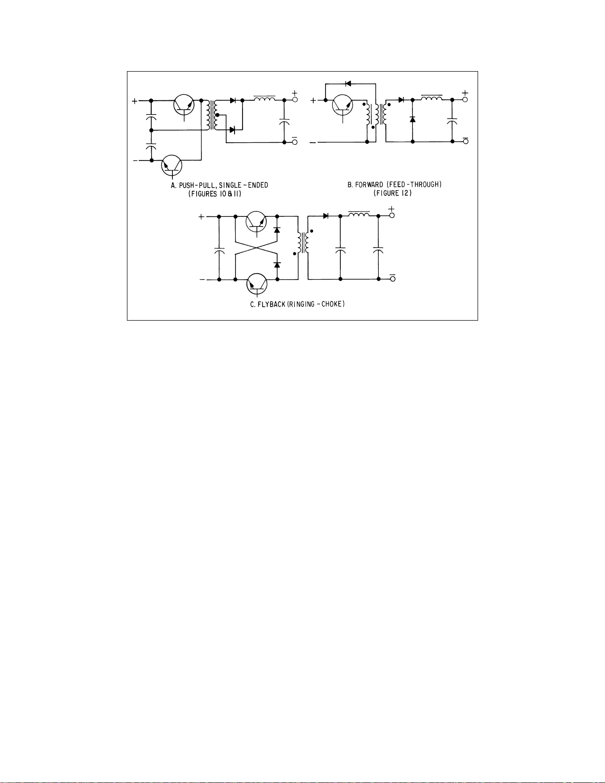
Figure 13. Basic Swit chi ng Regulator Configurations
Configuration B is a useful alternative to push-pull operation for lower power requirements It is called a
forward, or feed-through, converter because energy is transferred to the power transformer secondary
immediately following turn-on of the switch. Although the ripple frequency is inherently lower, output ripple
amplitude can be effectively controlled by the choke in the output filter. Two-transistor forward converters also
exist wherein both transistors are switched simultaneously. They provide the same output power as the single
transistor versions, but the transistors need handle only half the peak voltage.
Configuration C is known as a flyback, or ringing choke, converter because energy is transferred from primary
to secondary when the switches are off (during flyback). In the example, two transistors are used and both are
switched simultaneously. While the switches are on, the output rectifier is reverse biased and current in the
primary inductance rises in a linear manner. When the switches are turned off, the collapsing magnetic field
reverses the voltage across the primary, and the previously stored energy is transferred to the output filter and
load. The two diodes in the primary protect the transistors from inductive surges that occur at turn-off.
Flyback techniques have long been used as a means of generating high voltages (e. g., the high voltage power
supply in television receivers) and, as you might expect, this configuration is capable of providing higher output
voltages than the other two methods. Also, the flyback regulator provides a greater variation of output voltage
with respect to changes in duty cycle. Hence, the flyback configuration is the most obvious choice for high, and
variable, output voltages while the push-pull and forward configurations are more suitable for providing low,
and fixed, output voltages.
SCR Regulation
SCR regulation techniques permit the design of low cost, compact power supplies with efficiencies of
approximately 70%. Their main disadvantages are a higher ripple and noise, a less precise regulation, and a
slower transient recovery time relative to the other three regulation methods. However, these supplies are
widely used in high power applications where a lower degree of performance can be tolerated.
31
Page 31

Figure 14 illustrates a typical SCR regulated supply whose output is continuously variable down to near zero
volts. Circuit operation is very similar to the SCR preregulators described previously, except that the SCR
control circuit receives its input from the voltage comparison amplifier. The control circuit computes the firing
time for the SCRs, varying this in a manner which will result in a constant output despite changes in line
voltage or load resistance. The control circuit is capable of making a nearly complete correction within the first
half-cycle (8.3msec) following a disturbance.
Figure 14. SCR Regulated Power Suppl y
CONSTANT CURRENT POWER SUPPLY
The ideal constant current power supply exhibits an infinite output impedance (zero output admittance) at all
frequencies. Thus, as Figure 15 indicates, the ideal constant current power supply would accommodate a load
resistance change by altering its output voltage by just the amount necessary to maintain its output current at a
constant value.
Constant current power supplies find many applications in semiconductor testing and circuit design, and are
also well suited for supplying fixed currents to focus coils or other magnetic circuits, where the current must
remain constant despite temperature-induced changes in the load resistance. Just as loads for constant voltage
power supplies are always connected in parallel (never in series), loads for constant current power supplies
must always be connected in series (never in parallel).
32
Page 32

Figure 15. Ideal Constant Current Power Supply Output Characteristic
Any one of the four basic constant voltage regulators can also furnish a constant current output provided that its
output voltage can be varied down to zero, or at least over the output voltage range required by the load.
Besides the regulator, the reference and control circuits required for constant current operation are nearly
identical to those used for constant voltage operation. As a result of these many common elements, most
constant current configurations are combined with a constant voltage circuit in one Constant Voltage/Constant
Current (CV/CC) power supply.
The following paragraphs describe the current feedback loop generally employed in Agilent Technologies
CV/CC supplies. This particular approach to constant current, while sufficiently effective for most applications,
does have limitations that are caused by its simplified nature. For example, although output capacitor Co
minimizes output ripple and improves feedback stability, it also increases the programming response time and
decreases the output impedance of the supply; a decrease in output impedance inherently results in degradation
of regulation. If precise regulation, rapid programming, and high output impedance are required, improvements
on the basic feedback loop are necessary as described under Precision Constant Current Sources later in this
section.
Figure 16 illustrates the elements constituting a basic constant current power supply using a linear type
regulator. As mentioned previously, many of these elements are identical to those of a constant voltage supply
with the only basic difference being in their output sensing techniques. While the constant voltage supply
monitors the output voltage across its output terminals, the constant current supply monitors the output current
by sensing the voltage drop across a current monitoring resistor (RM) connected in series with the load .
The current feedback loop acts continuously to keep the two inputs to the comparison amplifier equal. These
inputs are the voltage drop across the front panel current control and the IR drop developed by load current I
L
flowing through current monitoring resistor RM. If the two voltages are momentarily unequal, the comparison
amplifier output changes the conduction of the series regulator, which in turn, corrects the load current (voltage
drop across RM) until the error voltage at the comparison amplifier input is reduced to zero. Momentary
unbalances at the comparison amplifier are caused either by adjustment of current control Ra, or by
instantaneous output current changes due to external disturbances. Whatever the cause, the regulator action of
the feedback loop will increase or decrease the load current until the change is corrected.
33
Page 33

Figure 16. Constant Current Power Suppl y
CONSTANT VOLTAGE/CONSTANT CURRENT (CV/CC) POWER SUPPLY
Because of its convenience, versatility, and inherent protection features, many Agilent supplies employ the
CV/CC circuit technique shown in Figure 17. Notice that only low power level circuitry has been added to a
constant voltage supply to make it serve as a dual-purpose source.
Two comparison amplifiers are included in a CV/CC supply for controlling output voltage and current. The
constant voltage amplifier approaches zero output impedance by varying the output current whenever the load
resistance changes, while the constant current amplifier approaches infinite output impedance by varying the
output voltage in response to any load resistance change. It is obvious that the two comparison amplifiers
cannot operate simultaneously. For any given value of load resistance, the power supply must act either as a
constant voltage or a constant current supply--it cannot be both. Transfer between these two modes is
accomplished automatically by suitable decoupling circuitry at a value of load resistance equal to the ratio of
the output voltage control setting to the output current control setting.
34
Page 34

Figure 17. Constant Voltage/Constant Current CV/CC Power Supply
Figure 18 illustrates the output characteristic of an ideal CV/CC power supply. With no load attached (RL= ∞),
I
= 0, and
OUT
= ES, the front panel voltage control setting. When a load resistance is applied to the output
EOUT
terminals of the power supply, the output current increases, while the output voltage remains constant; point D
thus represents a typical constant voltage operating point. Further decreases in load resistance are accompanied
by further increases in I
with no change in the output voltage until the output reaches Is, a value equal to the
OUT
front panel current control setting. At this point the supply automatically changes its mode of operation and
becomes a constant current source; still further decreases in the value of load resistance are accompanied by a
drop in output voltage with no accompanying change in the output current value. Thus, point B represents a
typical constant current operating point. Still further decreases in the load resistance result in output voltage
decreases with no change in output current, until finally, with a short circuit across the output load terminals.
I
= Is and EOUT = 0.
OUT
By gradually changing the load resistance from a short circuit to an open circuit the operating locus of Figure
18 will be traversed in the opposite direction.
35
Page 35

Figure 18. Operating Locus of a CV/CC Power Supply
Full protection against any overload condition is inherent in the Constant Voltage/Constant Current design
principle because all load conditions cause an output that lies somewhere on the operating locus of Figure 18.
For either constant voltage or constant current operation, the proper choice of ES and Is insures optimum protection for the load device as well as full protection for the power supply.
The slope of the line connecting the origin with any operating point on the locus of Figure 18 is proportional to
the value of load resistance connected to the output terminals of the supply. The "critical" or "crossover" value
of load resistance is defined as RC = ES/IS, and adjustment of the front panel voltage and current controls
permits the "crossover" resistance to be set to any desired value from 0 to ∞. If R
is in constant voltage operation, while if R
is less than RC, the supply is in constant current operation.
L
is greater than RC, the supply
L
CONSTANT VOLTAGE/CURRENT LIMITING SUPPLIES
Current limiting supplies provide overcurrent protection for applications where a constant voltage is the only
requirement. There are two basic types of current limiting circuits used today; conventional current limit and
current foldback
Current Limit
Current limiting is similar to constant current except that the current feedback loop uses fewer stages of gain.
Because of this, regulation in the region of current limiting operation is less precise than in constant current
36
Page 36

operation. Thus, the current limiting locus of Figure 19 slopes more than that of Figure 18, and the crossover
“knee" is more rounded.
A sharp knee indicates continuous regulation through the crossover region while a rounded knee denotes loss of
regulation before the crossover value is reached. To avoid any possibility of performance degradation, the
current limit crossover point must be set somewhat higher than the maximum expected operating current when
using a Constant Voltage/Current Limiting (CV/CL) Supply.
Figure 19. Current Limiting Characteristi c
CV/CL supplies employ either a fixed current limit or a continuously variable limit. In either case the change in
the output current of the supply from the point where current limiting action is first incurred to the current value
at short circuit is customarily 3% to 5% of the current rating of the power supply.
By their current limiting action, CV/CL supplies prevent damage to components within the power supply and
will also protect the load provided that the current limiting crossover point is set at a current value that the load
can handle without damage. All of Agilent's current limiting supplies are self restoring; that is, when the
overload is removed or corrected, the output voltage is automatically restored to the previously set value.
Current Foldback
Current foldback (Figure 20) provides better load protection than conventional current limiting because as the
load resistance decreases below the crossover value, both the voltage and current decrease simultaneously along
the foldback locus. The short circuit foldback point ranges typically between 20% and 50% of rated output
current with the exact point for a specific supply depending on design considerations and circuit tolerances.
For series regulated supplies, this reduction in short circuit output current decreases dissipation in the
37
Page 37

regulating elements. Thus, current foldback is especially useful if the supply is operating in a remote location
and a long term short-circuit occurs. For switching regulated supplies, current foldback does not significantly
reduce dissipation within the supply. It does, however, provide superior load protection as mentioned
previously.
All Agilent supplies that employ current foldback are self restoring and are designed to withstand worst case
dissipation, which occurs under partial overload conditions when the supply is operating along the upper half of
the foldback locus.
Foldback current limiting is incorporated more often into fixed output voltage supplies because full rated output
current can be obtained only at the maximum rated output voltage. As indicated in Figure 20, reductions in
output voltage are accompanied by linear decreases in the available output current. Conventional current
limiting techniques, on the other hand, are used mostly in supplies that furnish continuously variable output
voltages. Note in Figure 19 that maximum rated current can be obtained at any rated output voltage.
Figure 20. Current Foldback Characteristic
PROTECTION CIRCUITS
Today, many power supply manufacturers are placing increasing emphasis on protection for both the power
supply and its load. A supply with extensive protection networks is of obvious benefit to the user, particularly
if used in a crucial application such as a system power source or in the testing of critical components.
Protection Circuits for Linear Type Supplies
The following paragraphs describe protection circuits that are commonly used in Agilent series regulated and
series/preregulated type supplies (Figure 21).
A. Varistor - A voltage-dependent resistor that protects preregulator triac against ac line spikes. Its resistance
decreases abruptly if line voltage exceeds a harmful level.
38
Page 38

B. RFI Choke - Minimizes spikes at output of supply by slowing down turn-on of triac.
C. Rectifier Damping Network - RC network protects other elements in supply against short-duration input
line transients.
D. Series Regulator Diode - Protects the series regulator against reverse voltages which could be delivered by
an active load or parallel power supply.
E. Slow Start Circuit - A long time-constant network that reduces turn-on overshoot and helps limit inrush
current. When supply is first turned on, this circuit holds off both the series regulator (to reduce output
overshoot) and the preregulator triac (to limit inrush current).
F. Amplifier Input Clamp Diodes - Limit the maximum input to the amplifier to protect it against excessive
voltage excursions.
G. Output Diode - Protects components in the power supply against reverse voltages that might be generated
by an active load or series connected power supply.
H. Sensing Protection Resistors - Protect the load from receiving full rectifier voltage if remote sensing leads
are accidentally open-circuited.
Figure 21. Protection Circuits, Li near Type Supply
Overcurrent and Overvoltage Protection - All Agilent supplies are short-circuit proof and can operate under any
current overload condition indefinitely without risk of internal damage. Overvoltage protection is also available
if required during constant current operation. The CV/CC and CV/CL automatic crossover circuitry discussed
previously is ideal for these purposes since it allows the user to select the maximum safe current or voltage for
the particular load device.
Overvoltage Crowbar - The crowbar circuit is connected across the output terminals, and provides protection
against any output overvoltage condition which might occur because of operator error or failure within the
power supply or load. Most Agilent power supplies of this type have either a built-in or optional crowbar
circuit. Because of its importance in many applications, the crowbar circuit is discussed in more depth on the
following pages.
Overvoltage Crowbar Circuit Details
An operator error or a component failure within the regulating feedback loop can drive a power supply's output
voltage to many times its preset value. The function of the crowbar circuit is to protect the load against this
39
Page 39

possibility. The circuit insures that the power supply voltage across the load will never exceed a preset limit.
This protection is valuable because of the extreme voltage sensitivity of present-day semiconductor devices.
The basic elements used in most crowbars are: some method of sensing the output voltage, an SCR that will
short the output, and a circuit that will reliably trigger the SCR within a time period that is short enough to
avoid damage to the load.
The sense circuit can be a simple bridge or voltage divider network that compares the output voltage to some
internal crowbar reference voltage. The best trigger circuit is the one that turns the SCR on the fastest. Fastest
SCR turn-on is accomplished by a fast rise-time pulse circuit such as a blocking oscillator or Schmitt trigger.
The Agilent Technology crowbar, illustrated in Figure 22, compares the output voltage with a reference voltage
+ V. The overvoltage potentiometer adjusts the reference voltage on the comparison amplifier and sets the
voltage level at which the crowbar will activate. Normally the overvoltage control is located on the front panel
and can be adjusted from approximately 20% to 120% of the maximum rated output voltage of the power
supply.
Figure 22. Typical Crowbar Overvoltage Protection Circuit
When the output voltage exceeds the reference, the comparison amplifier triggers the blocking oscillator which
then sends firing pulses to the SCR. When the SCR fires, it places a very low impedance across the output,
reducing the voltage to near-zero.
Several beneficial features are included in most Agilent crowbar circuits:
1. An overvoltage indicator lights when the SCR fires; the lamp conducts a holding current to prevent the SCR
from oscillating on and off.
40
Page 40

2. The crowbar circuit creates an extra current path during normal operation of the supply, thus changing the
current that flows through the current monitoring resistor. Diode CR1 keeps this extra current at a fixed
level for which compensation can then be made in the constant current comparator circuit.
3. In preregulated supplies the crowbar turns off the preregulator circuit when the SCR fires, reducing the
voltage drop across the series regulator and the current flow through the SCR.
4. An auxiliary winding is included on the blocking oscillator transformer for connection to an additional
crowbar. Tandem crowbar operation is then available for coincident firing of all crowbars in a system.
Crowbar Response Time
The crowbar's speed of response to an overload is a critical parameter. If the response time is too slow, the
output could rise to a level high enough to damage the load. If the response is too fast, then spurious noise can
cause false tripping and create a nuisance condition.
There are three time delays that place a practical limit on how fast crowbars can react. In order of decreasing
magnitude, they are:
(1) The typical SCR turn-on time (from lµsec to around 5µsec);
(2) The reaction time of the trigger circuit; and
(3) The time delay associated with the crowbar voltage-sensing circuit. Since only a fraction of the output
voltage is compared with an internal crowbar reference voltage, the voltage sensing circuit incorporates a
large voltage divider which combines with discrete and stray capacitance in the sensing circuit to form an
RC delay network.
If the output voltage is rising relatively slowly there will be essentially no time delay of types (2) and (3). The
SCR will be triggered within a fraction of a microsecond after the relatively slow-rising output voltage crosses
the trip level, and the only noticeable time delay will be the turn-on time of the SCR. If, on the other hand, the
output voltage waveform approaches a step, the sense circuit will not follow the fast rising wavefront and an
added time delay (type 3) will result. For a step that is only a few millivolts above the trip level, this time delay
can be as much as a few microseconds; but as the magnitude of the step increases, the sense circuit charges
faster and the delay decreases.
In practice, it is unrealistic to specify either the time delay or the maximum overvoltage as shown in Figure
22A, because they vary according to operating levels, load and line impedances, and the exact failure mode.
Instead Agilent Technologies specifies the overvoltage trip margin, which is defined as "the minimum crowbar
trip setting above the desired operating output voltage to prevent false crowbar tripping".
41
Page 41

Figure 22A. Crowbar Response
Figure 23 shows typical protection circuits that are used in Agilent switching regulated power supplies. Most of
these protection circuits perform functions that are similar to those of the linear supply of Figure 21. However,
their circuit placement, or the manner in which they affect the operation of the supply, is often different.
Several protection circuits (such as the ac undervoltage detector) are required only in switching supplies.
The following is a brief description of the protection circuits shown in Figure 23.
A. RFI Filter- Helps prevent RFI spikes from being conducted to the load or back into the ac line. Agilent
switching supplies also contain built-in shields for additional control of conducted and radiated
interference.
B. Thermistor - Limits ac inrush current by its negative temperature coefficient of resistance. Has a high
resistance when cold (during turn-on) and low resistance after it heats up.
C. Regulator Overcurrent Limit - This circuit is much faster than the current limit comparator and protects the
regulator switches from overcurrent conditions of a transient nature. It monitors current flow through the
switches and prevents it from exceeding a harmful level.
D. Output Rectifier Diodes - Besides final rectification, these diodes also protect internal components against
reverse currents that could be injected into supply by an active load or series connected supply.
E. AC Undervoltage - Performs a dual function. Protects supply from damage that could result from a
prolonged condition of low ac input voltage and limits output overshoot during turn-on. During
undervoltage or turn-on conditions, the low ac input level reduces the V
voltage and activates the
BIAS
undervoltage detector. When activated, the modulator pulses are inhibited and the regulator switches turned
off.
F. Overvoltage Detector- Monitors output voltage and turns-off regulator switches if output attempts to rise
above a preset value. Similar to crowbar circuit described previously, except that output voltage is removed
by turning off regulator rather than by shorting the output.
G. Temperature Switch - Opens in case of high ambient temperature that could be caused, for example, by a
misapplication or cooling fan failure. Opening switch removes V
and activates ac undervoltage detector.
BIAS
Switch closes again after temperature cools to a safe level.
42
Page 42

Figure 23. Protection Circuits, Switching Type Supply
Additional Protection - Although not shown on Figure 23, all Agilent switching supplies contain some form of
overcurrent protection, usually a current foldback circuit. Also included are remote sensing protection resistors
and input protection components for the comparison amplifier.
SPECIAL PURPOSE POWER SUPPLIES
High Voltage Power Supply
Normal series, switching, or SCR regulation techniques may not be suitable for all-semiconductor,
short-circuit-proof power supplies with outputs greater than 300 volts. For example, in a series regulated
supply, shorting the output terminals would place the rectifier voltage (more than 300 volts) across the series
transistors. Utilizing a sufficient number of high voltage series transistors to achieve output of several thousand
volts would be too costly and unreliable. Even the preregulator circuit of Figure 7 is not suitable for a higher
voltage supply, because a shorted output causes the rectifier capacitor to discharge through the series regulator,
and the energy stored in this capacitor is enough to destroy the power transistors in the regulator.
High voltage Agilent supplies utilize a circuit technique that extends the usefulness of series regulating
transistors rated for 30 volts to short-circuit-proof power supplies rated for outputs of well over 3000 volts. As
shown in Figure 24, the basic technique consists of placing a well-regulated low voltage power supply in series
with a less-well-regulated high voltage supply. Notice, however, that the amplified error signal from the voltage
comparison amplifier is dependent upon the total output voltage -- not just the output of the low voltage power
supply alone. Thus, the well-regulated "piggyback" supply continuously compensates for any ripple, load
regulation, or line regulation deficiencies of the main power source by adjusting the voltage across its series
regulator to maintain the total output voltage at a constant level.
43
Page 43

Figure 24. "Piggy-back" Power Supply
As an illustrative example, assume that the low voltage rectifier supplying the series transistor of the "piggyback" supply develops approximately 40 volts, and that the main voltage source is capable of providing a
maximum of 300 volts. With 20 volts normally dropped across the series regulator, the maximum output of this
supply would be 320 volts; 20 volts from the "piggy-back" supply and 300 volts from the main source. Thus,
the series regulator of the "piggy-back" supply would have a ± 20 volt range available for accomplishing the
dynamic changes necessary to compensate for the output voltage variations of the main source.
Short-circuit protection for the series regulator in the "piggy-back" supply (Figure 24) is provided by diode CR
which, if the output terminals are shorted, provides a discharge path for rectifier capacitor CM. Since CR
P
prevents the output of the "piggy-back" supply from ever reversing polarity, the series regulator will never be
called upon to withstand a voltage greater than the 40 volts from its own rectifier.
Fuse F1 is included so that the path between the output terminals and the rectifying elements of the main
voltage source will be opened under overload conditions, to protect the rectifiers and transformer.
The high voltage control circuit does not derive its input control signal from the total voltage across the load
resistor or the voltage across the terminals of the high voltage supply itself. Instead, the control circuit monitors
the voltage across the combination series regulator and current monitoring resistor and maintains this voltage
44
P
Page 44

drop at approximately 20 volts, leaving approximately 20 volts across the output terminals of the "piggy-back"
supply.
Agilent Technologies supplies may use any of three basic methods of controlling the high voltage output of the
Main Voltage Source: (1) the control signal from the High Voltage Control Circuit fires SCRs in the rectifier
circuit to vary the dc output, (2) the control signal varies the coupling of the high voltage input transformer to
adjust the ac input to the rectifiers or (3) the control signal pulse modulates the input to the rectifier to vary the
dc output.
High Performance Power Supplies
Agilent Technologies manufactures several types of high performance dc power supplies with specifications at
least an order of magnitude superior to the normal well-regulated laboratory supply. Foremost among these are
the precision voltage and current sources.
Precision Voltage Sources
This line includes both CV/CC and CV/CL supplies, similar to those described previously, with a
few important exceptions. The critical components of the supply, including the zener reference
diode for the voltage comparison amplifier and the low-level portions of the feedback amplifier, are
enclosed in a temperature-controlled oven. Moreover, the less critical components that are not oven
enclosed are high quality components with low temperature coefficients. These techniques, together
with the utilization of a high-gain feedback amplifier, result in an exceptionally stable and
well-regulated supply with a 0.1% accuracy.
Precision Constant Current Source
The concepts and circuits used in basic constant current power supplies were shown in Figure 16.
This section is devoted to the refinements necessary to upgrade a basic constant current supply to a
precision class, with characteristics that more closely approach an ideal current source.
An ideal current source is a current generator that has infinite internal impedance. It provides any voltage
necessary to deliver a constant current to a load, regardless of the size of the load impedance. It will supply this
same current to a short circuit, and in the case of an open circuit it will attempt to supply an infinite voltage (see
Figure 25).
In practical current sources, neither infinite internal impedance nor infinite output voltages are possible. In fact,
if the current source is to be used as a test instrument, it should have a control for limiting its maximum output
voltage, so its load will be protected against the application of excessive potentials. Its output impedance should
be as high as possible, of course, and should remain high with increasing frequency to limit current transients in
rapidly changing load. A capacitor across the output terminals should be avoided, since it will lower the output
impedance, store energy which can result in undesirable current transients, and decrease the programming
speed.
One approach to the design of a current source is to add a high series resistance to an ordinary voltage source.
However, it is difficult to achieve good current regulation with this design.
Typical applications for current sources call for output impedances of a few megohms to a few hundred
megohms and currents of tens or hundreds of milliamperes. This means the source voltage would have to be
45
Page 45

tens of kilovolts or more. Such a high-voltage supply would cause noise problems, would be difficult to
modulate or to program rapidly, would be dangerous, very large, and would waste considerable power.
Figure 25. An Ideal Current Source
Electronic current regulation is a much more tractable way to obtain high output impedance, although there are
still design problems, such as leakage.
Leakage Versus Regulation. The current regulation of a current source, as seen at the load, is degraded by any
impedance in parallel with the load. If I
impedance, and Z
is the total impedance shunting ZL, then
S
I
IL =
O ZS
Z
L
+ Z
is the current generated by the source, IL is load current, ZL is load
O
S
When the output impedance of the current source is high, then even very small leakage currents can become
significant (see Figure 26). Such things as the input impedance of a voltmeter measuring the load voltage, the
insulation resistances of wiring and terminal blocks, and the surface leakage currents between conductors on
printed circuit boards will all take current away from the load, unless special design precautions are used.
Agilent Current Sources. In Agilent Technologies Current Sources, leakage at the output terminals is
negligible, owing to a combination of techniques, including guarding, shielding, and physical isolation.
Feedback regulation makes the output impedance high (3.3 to 10,000 megohms), and there is no output
capacitor to lower the output impedance or store energy. Low leakage and high output impedance result in
precise current regulation.
46
Page 46

Figure 26. Impedances Shunting the Load Degrade Current Regulat i on
As shown in Figure 27, the CCB design includes three key sections which determine its unique regulating properties--the Programming/Guard Amplifier, the Main Current Regulator, and the Voltage Limit Circuit.
The Programming/Guard Amplifier is an independent, variable constant voltage source, whose output voltage
E
is linearly dependent upon the setting of RQ, being equal to ESRQ/RS. The guard aspects of this circuit are
G
discussed in detail later; it is sufficient to note here that this circuit permits linear output current control while
facilitating the common point connection at the inboard side of the current monitoring resistor.
The Programming/Guard Amplifier provides the programming voltage E
for the Main Current Regulator; this
G
dc voltage, which is negative with respect to circuit common, is applied to one of the inputs of the differential
Current Comparison Amplifier. The other input of this differential amplifier is connected to the current
monitoring resistor R
current monitoring resistor (I
. The Current Comparison Amplifier continuously compares the voltage drop across the
M
) with the programming voltage (EG). If these voltages are momentarily
ORM
unequal due to a load disturbance or a change in the output current control setting, this error voltage is
amplified and applied to the series regulator transistors, altering the current conducted through them and forcing
the voltage drop I
to once again equal EG.
ORM
The output current is related to the programming voltage and reference voltage by the relationship
IO =
E
G
R
M
E
S
=
R
M
R
Q
•
R
S
As this equation suggests, RM is a critical component and is selected to have low noise, low temperature coefficient, and low inductance.
47
Page 47

Its ohmic value is large enough to give an adequate current monitoring voltage, yet small enough to minimize
its temperature rise (and the resulting resistance change) caused by its own power dissipation.
Figure 27. Precision Current Source Block Diagram
Returning to the guard duties of the Programming/Guard Amplifier, the output of this amplifier (E
G
) is
connected to a guard conductor which surrounds the positive output terminal, the current monitoring resistor,
and the (+) input to the Current Comparison Amplifier. Since E
is held at the same potential as the positive
G
output terminal by the Main Current Regulator, no leakage current flows from the positive output terminals (or
any of the internal circuit elements connected to it). The leakage currents that would normally flow from the
positive output circuitry flow instead from the guard conductor, whose current is supplied by the
Programming/Guard Amplifier. Notice that since the Programming/Guard Amplifier is a low impedance source
referenced to (C), any leakage current fed by the guard originates from circuit common via this amplifier,
bypassing RM--only the output current flows through RM. In this way leakage current flowing directly between
the supply's two output terminals is eliminated, and precise load regulation is obtained.
The Programming/Guard Amplifier output may also be used as a convenient point to connect indicating meters,
since the current to drive these meters will not affect the regulated output current I
O.
The Voltage Limit Circuit is designed to eliminate dangerous high-voltage or high-current transients that might
occur under certain load conditions. For example. when the load is suddenly removed from an ordinary
constant-current power supply, the output voltage attempts to rise to the raw supply voltage of the instrument,
which can be hundreds of volts. Or, when the load is suddenly reconnected to a supply operating in the voltage
48
Page 48

limit mode, a high-current transient can occur if the current regulator saturates while the instrument is still in
voltage limit.
The Voltage Limit Circuit in Constant Current Sources virtually eliminates voltage or current overshoots and
undershoots when going in and out of voltage limit, without adding any significant leakage path across the
output terminals.
Normally, when voltage limiting action is not occurring, the setting of the Voltage Limit Control establishes
across the Shunt Voltage Regulator a preset voltage limit EL which is higher than the positive output voltage
and its twin, the guard voltage EG. Since there is zero volts across the series combination of isolation diode
CR2 and resistor R1 (5 kilohms or less), no current flows through them, and potential EG is also present at their
junction, thus back-biasing isolation diode CR1. (Any small leakage through back-biased diode CR1 flows
through R1 and the output of the Programming/Guard Amplifier, but does not flow into CR2 or the positive
output terminal). The Shunt Voltage Regulator conducts a “standby” current through shunt regulator bias
resistor RB; this current insures that the Shunt Voltage Regulator is operating in its linear region, ready to react
quickly when voltage limiting action is required, thus preventing crossover transients.
If the output voltage exceeds the preset voltage limit value CR1 and CR2 conduct, and the Shunt Voltage
Regulator conducts a portion of the current which otherwise would flow to the load, thus clamping the output
voltage to the preset limit value.
Even during voltage limiting action, E
continues to be maintained at a value equal to the potential at the
G
positive output terminal; both guarding action and the normal control action of the Main Current Regulator
continue, minimizing any output transients which might tend to occur when the output transfers from voltage
limiting to its normal output current mode.
High Output Impedance. The high output impedance of these current sources is a result of several factors,
both electrical and mechanical. The series-regulator transistors are in a cascade configuration, which inherently
has a high output impedance. Since the open-loop gain of the error amplifier is high, the closed-loop output
impedance is greatly increased by feedback.
Output capacitors have been eliminated -- and although the output impedance falls off with frequency because
of the necessary gain and phase compensation in the amplifier circuits, it is much higher than it would be if a
capacitor were connected across the output terminals.
The importance of low output capacitance should not be underestimated. Excessive output capacitance would
cause the output impedance of the current source to fall off with increasing frequency, producing undesirable
transients in rapidly changing loads. Large capacitors store large amounts of energy which, if discharged suddenly through the load, may cause damage; negative-resistance devices are particularly susceptible to this kind
of damage. Finally, an output capacitor would slow down the response of the current source to changes in the
external programming signal.
In the interest of keeping the output impedance high, the impedances of internal leakage paths have been made
as high as possible by careful mechanical design and hygienic construction techniques. Leakage, both internal
and external, is further reduced by guarding the positive output terminal.
Guarding. In addition to eliminating leakage currents, the guard can also be used to measure the output voltage
without drawing current away from the load. Connecting a voltmeter between the negative output terminal and
the positive output terminal will lower the output impedance, but a voltmeter connected between the negative
49
Page 49

output terminal and the guard has no effect on the output impedance. The meter still measures the output
voltage because the guard is at the same potential as the positive output terminal. The front-panel voltmeter is
internally connected to guard; and if greater accuracy is needed, a voltmeter can be connected externally.
Unlike other guards, such as those used on digital voltmeters, the guard in the Current Source is active and
internally referenced to the positive terminal. For this reason the guard is labeled "(+) meter" on the front panel.
and must not be connected to either output terminal, since this interferes with the closed loop performance.
Transformer Shielding Eliminates Ripple. Agilent Current Sources meet their low ripple specifications
regardless of which output terminal, if either, is connected to earth ground. High-gain current regulation is one
reason for the low ripple. Another is special shielding to keep ac voltages in the power transformer from being
coupled into the output via the capacitance between the transformer windings and the output or ground.
One potential source of ripple current is capacitive coupling between the primary winding and the negative
output terminal. This problem is eliminated by enclosing the primary winding in an electrostatic shield which is
connected to earth ground. A second source of ripple current is capacitive coupling between the secondary
winding and ground. To keep this current from affecting the output, the secondary winding is enclosed in an
electrostatic shield which is connected to the negative output terminal. This causes the ripple current generated
by the secondary winding to be confined to a closed loop inside the instrument.
Extended Range Power Supplies
This type of supply automatically extends the number of output voltage and current combinations that are
available within the maximum power rating of a single unit. Before discussing circuit techniques, the following
paragraphs first outline the advantages of the extended range concept itself.
Advantages of Extended Range
Figure 28 compares the output characteristic of a conventional CV/CC supply with that of an extended range
supply of the same output power (200W in the example). As indicated in 28(A) maximum output power from a
conventional supply can be obtained at only one point (20V/10A) on its rectangularly shaped locus. Maximum
output power for an extended range supply, however, is available not only at 20V/10A, but at 50V/4A and
anywhere along the curved portion of the characteristic ranging between 20 and 50V.
To duplicate this capability would require either one large 500W power supply operating inefficiently at less
than rated output at many operating points, or else several equivalent supplies; a 50V/4A supply, a 20V/10A
supply, and others for in-between voltage and current ratings. Both of these solutions are expensive and require
a significant amount of bench or rack space.
50
Page 50

Figure 28. Output Characteristics of CV/CC Supplies, Conventional vs. Extended Range
Example of Extended Range Power Supply
Agilent Technologies uses two different design techniques in their extended range power supplies. In one type,
shown on Figure 29, extended range is achieved by adding a special tap switching network ahead of a standard
CV/CC series regulated feedback loop. A more recent design, utilizes a regulator type whose output
characteristic naturally assumes the shape of Figure 28(B), without the need for an electronic tap switching
network. However, for convenience, only the extended range supply with the tap switching network is
described in the following paragraphs.
This supply achieves the high level of performance normally associated with a preregulated/series regulated
supply; plus two additional advantages. The first advantage is the extended range concept described previously
and the second is that the programming speed is considerably faster than a comparable preregulated unit.
The simplified schematic of Figure 29 shows that this supply consists basically of a CV/CC series regulator
feedback loop preceded by an electronic tap switching network. Operation of the main series regulator loop is
virtually identical to many other supplies developed by Agilent Technologies. The tap switching circuits,
however relate only to extended range supplies and it is these circuits that govern the overall output
characteristic of Figure 28(B).
Electronic Tap Switching. As shown on Figure 29, tap switching is accomplished by a pair of triac switches
(CR1 and CR2) and an associated control circuit. By selecting different triac firing combinations, these circuits
allow the input capacitor (Cl) to charge to one of four discrete voltage levels, depending on the output voltage
and current required.
51
Page 51

The main secondary winding of the power transformer has three sections, each of which has a different turns
ratio with respect to the primary winding. At the beginning of each half-cycle of the input ac, the control circuit
determines whether one, both, or none of the triacs will be fired. If neither triac is fired, the rectifier receives an
ac input voltage that is determined by N1 turns and the input capacitor charges to a corresponding level. If triac
CR2 is fired, capacitor Cl charges to voltage determined by N1 + N2 turns. Similarly, if CR1 is fired the
capacitor is charged by N1 + N3. Finally, if both triacs are fired simultaneously, Cl charges to its highest
voltage level (N1 + N2 + N3).
Figure 29. Extended Range Power Supply Using Tap Switching
The triac control circuits determine which triac is to be fired by monitoring the output voltage and current (IR drop across
current monitoring resistor, RM) and comparing these values against a set of three internally derived reference levels. These
reference levels are translated into boundary lines to allow the output characteristic to be mapped into four operating regions
(Figure 30). The boundary lines, which are invisible to the user, are named VOD for output voltage "decision" line, and
IOD1 and IOD2 for output current "decision" lines one and two. Whenever the output voltage is below the sloping VOD
line, the control circuit inhibits both triacs and the input capacitor charges to a voltage determined
by N1. Whenever the
output voltage is greater than the VOD line, the control circuit looks at the output current level to determine
which triac should be fired. Figure 30 indicates the windings that are connected as a result of the current
decisions.
52
Page 52

Figure 30. Output Power Pl ot
The triac control circuit also monitors the unregulated dc to provide ac line compensation. Variations in the
amplitude or frequency of the ac line modify the amplitude of the unregulated dc voltage which, in turn, alter
the position of the IOD1 and IOD2 decision lines. For example, both IOD lines decrease (move to the left) if the
ac line voltage increases. The reverse occurs if the ac line voltage decreases. This action prevents excessive
regulator dissipation during periods of high line yet assures an adequate voltage drop across the series regulator
during periods of low line.
Noise Reduction. Triacs, as well as any other switching devices, can generate a considerable amount of EMI.
Because this interference is proportional to the turn-on dv/dt, the triacs in this supply are fired only when the
voltage across them is low, thus minimizing EMI. The current through the triacs, however, must be higher than
the minimum latching current that is required to sustain conduction. Thus, triac firing must occur late enough in
the ac input cycle for the current to be above the latching level yet early enough in the cycle so that the dv/dt
will not generate excessive EMI.
Faster Down-Programming Speed
As mentioned previously, the programming speed of this unit is considerably better than that of the preregulated
power supplies that exist at this power level. Up-programming is not a particular problem in either type of unit
because it is aided by the conduction of the series regulator. Down-programming, however, is much slower in a
preregulated unit because: (1) an active element is not normally available to aid in the discharge of the output
capacitor and (2) any decrease in the charge across the output capacitor must be accompanied by a decrease in
the voltage across the input filter capacitor to avoid damaging the series regulator. This problem exists because
the series regulator, which normally operates with a Vce of only a few volts, does not have the heat sink
capability to absorb the extra energy dissipated when discharging the filter capacitor during
down-programming.
53
Page 53

The extended range power supply overcomes the latter problem through the use of series regulating transistors
with higher voltage ratings and with thermally improved heat sinks. The heat sinks allow the series transistors
to be properly cooled during the worst case conditions that are encountered during rapid down-programming. In
addition, a special transistor circuit (not shown on Figure 29) provides for a more rapid discharge of the output
capacitor during down-programming.
Bipolar Power Supply/Amplifier
In some applications a power supply is required that has a faster programming speed than standard designs (see
Remote Programming Chapter for programming speed limitations). Still other applications require a power
supply that can be controlled continuously through zero over a wide span in either the positive or negative
direction. Bipolar Power Supply/Amplifiers (BPS/As), which utilize the operational amplifier concept of power
supplies, have been developed to meet these needs. A BPS/A is not only a high speed, programmable power
supply but can also be used as direct-coupled amplifier with low output distortion and a bandwidth from dc to
as high as 40KHz (in certain operating modes).
Bipolar Power Supply
Figure 31 shows a simplified representation of the instrument drawn as a CV/CC power supply. Note that this
circuit differs from the typical CV/CC power supply of Figure 17 in that:
1. The regulating elements consist of two series transistors connected in a push-pull, pseudocomplementary
configuration (Q1 and Q2 are actually npn's). Q1 is connected to a positive rectifier and controls positive
outputs while Q2 (connected to a negative rectifier) controls negative outputs.
2. A bipolar CV reference source is used instead of a unipolar one to allow a bipolar output in the constant
voltage operating mode.
3. Two current comparison amplifiers and an associated bipolar reference source, are used to provide a bipolar
output in the constant current mode.
4. The output capacitor has been eliminated to increase programming speed. Additional modifications, not
shown in Figure 31, insure that the power supply will remain stable for capacitive, resistive, or inductive
type loads.
Aside from the above differences, basic operation of this bipolar power supply is very similar to most other
CV/CC supplies. The CV or CC comparison amplifiers compare the output voltage (or current) with the bipolar
reference and generate amplified error signals that control the conduction of the applicable regulating transistor
(Q1 or Q2).
Amplifier
Figure 32 shows the BPS/A redrawn as an amplifier. Transistors Q1 and Q2 are arranged in a single-ended,
push-pull configuration, and the operational amplifier aspects are more readily suggested by this configuration.
For simplicity, the constant current control circuits are not included in Figure 32. In the amplifier mode, the
BPS/A controls the gain of an externally applied dc or ac signal. In Figure 32, an external ac input signal has
been substituted for the internal bipolar reference supply shown in Figure 31.
54
Page 54

Figure 31. Bipolar Power Suppl y/Amplifier Draw n as a CV/CC Power Supply.
The rear terminal strip on BPS/A instruments includes numerous control terminals to facilitate remote
resistance programming of the CV or CC output in the power supply mode or remote dc or ac programming in
the amplifier mode.
Digitally Controlled Power Sources
Digitally controlled power sources (DCPS's) are designed specifically for use in modern automated systems
which require power supplies capable of being programmed by a digital controller. Although tailor-made for
computer-based automatic test systems, DCPS interface circuitry can be readily modified to permit control by a
programmable calculator, coupler, or other digital data source. The basic function of the DCPS is to convert the
digital signals from the controller into analog form with speed and accuracy.
Agilent Technologies’ family of DCPS's includes several digital voltage sources and one current source.
Digital Voltage Source (DVS)
The DVS is a Constant Voltage/Current Limiting power source that can be continuously programmed
throughout its bi-polar output voltage range. Figure 33 is a simplified block diagram showing a typical DVS
manufactured by Agilent. The unit consists basically of a digital-to-analog (D/A) converter followed by a
bi-polar power amplifier.
55
Page 55

Figure 32. Bipolar Power Supply/Amplifier Draw n as an Amplifier
56
Figure 33. Digital Voltage Source Bl ock Di agram
Page 56

Additional circuits are also included to facilitate operation within the systems environment. The additional
circuitry performs interface, isolation, storage, overcurrent protection, and status feedback functions as
explained in subsequent paragraphs.
Interface and Isolation. Each input and output signal, to and from a DCPS, passes through interface and
isolation circuits. Interface circuits are designed to match the unit to a variety of controllers. Isolation circuits
isolate the digital input from the analog output voltage allowing the output to be floated if desired. Isolation
also prevents troublesome loops between the output ground and controller ground and prohibits potentially
destructive current surges which could occur if some point in the load were inadvertently grounded.
Storage. The digital voltage and current programming input data are transferred into integrated-circuit storage
buffers upon receipt of the storage pulse from the controller. Once the data is stored, the controller can perform
other tasks without the need for maintaining the input data. This increases controller operating efficiency and
even allows "party-line" operation where one set of data lines can be used to program several DCPS.
The storage capability also minimizes voltage programming overshoots or undershoots by ensuring that all
voltage program inputs reach the D/A converter simultaneously. The gate pulse is delayed 50µsec from the
arrival of the input data to allow time for all input lines to settle.
If the programming source does not normally generate gate signals, the storage circuits can be bypassed by
means of a switch on the DVS. The voltage program data now passes directly into the D/A converter as soon as
received from the isolation circuits, but without the benefit of storage.
D/A Converter. The heart of a DCPS is the D/A converter. This bi-polar, high-speed circuit converts the digital
voltage programming inputs into an analog reference signal which drives the precision power amplifier. The
reference output signal is either positive or negative in accordance with the polarity of the input data.
Bipolar Power Amplifier. The accurate reference signal from the D/A converter goes directly to the power
amplifier. To preserve the accuracy of the input signal, large amounts of negative feedback are used in the
amplifier circuits. The amplifier can be programmed either side of, or through, zero without "notch" effects or
the use of polarity switches.
The power amplifier has a self-contained voltage limit circuit which prevents the output voltage from exceeding
110% of rating despite possible programming errors. It also contains a "gross" current limit circuit which
prevents the output current from exceeding 110% (maximum) of the rated output current. This circuit provides
backup protection for the programmable overcurrent circuits.
Overcurrent Protection. Both the load and the DVS are protected against overcurrent conditions by a current
comparator and latch circuit. When activated, this circuit sends a latch signal to the power amplifier which
shuts off the output stages and reduces the output current to under 10% of the current rating. The current latch
trip point can be programmed, by three external current latch program bits, to one of eight values ranging from
2% to 100% of the output current rating. The current latch bits from storage are first converted to a
corresponding analog reference value within the current comparator and latch circuit. Next, this reference value
is compared with a sample of the output current (IOUT). If the output current equals or exceeds this reference
value, a current overload condition exists. Approximately 5µsec after a current overload is detected; a latch
signal is generated to reduce the output current. Should the load require a heavy initial current, the delay period
between overload and latch can be extended up to 2msec by adding an external capacitor.
57
Page 57

Status Feedback. Three feedback lines are available to furnish continuous status information to the controller.
A flag line informs the computer when new voltage programming data is being processed by the DVS. Current
overload and latch lines are activated if the DVS experiences a current overload or latch condition.
Digital Current Source (DCS)
The DCS is a bipolar Constant Current/Voltage Limiting power source. A DCS unit contains most of the same
circuit elements that were shown for a DVS unit; including, interface and isolation circuits, storage, D/A
converter, and a bi-polar output amplifier. One difference is, of course, that a DCS unit has a programmable
voltage limit circuit rather than a programmable overcurrent circuit. The voltage limit circuit returns two
overload status signals to the controller in a manner similar to the DVS overcurrent circuit.
The DCS also employs guarding techniques that are conceptually identical to those of the Precision Constant
Current Source described earlier in this section. As mentioned previously, these guarding techniques prevent
the flow of leakage current and allow a more precise regulation of the output current.
58
Page 58

AC AND LOAD CONNECTIONS
Modern power supplies are flexible, high-performance instruments designed to deliver a constant or controlled
output with a maximum of reliability and control versatility. In many cases, however, the user inadvertently
degrades this performance capability by making improper wiring connections to the input or output. At best,
this can result in excessive output ripple, a tendency toward oscillation, poor load and line regulation, and
unnecessary degradation of stability, temperature coefficient, and transient recovery specifications. At worst,
the result can be power supply failure and potential shock hazards.
Careful attention to the guidelines presented in this section will improve the safety and usefulness of power
supplies. As a general rule, the guidelines should be followed in the sequence given, e. g., dc distribution
terminals must be considered before common or ground connections.
The following checklist is included for quick reference to the most important rules in connecting dc power
supplies; these rules are repeated with greater detail on the pages indicated.
CHECKLIST FOR AC AND LOAD CONNECTIONS
Each rule should be followed in the sequence indicated.
AC Power Input Connections
Page
1. The ac, acc and third wire safety ground continuity should be retained without accidental
interchange from ac power outlet to the power supply input terminals.
2. If an autotransformer (or isolation transformer) is connected between the ac power source and
the power supply input terminals, it should be rated for at least 200% of the maximum rms
current required by the power supply.
3. The autotransformer common terminal should be connected to the acc (not ac) terminals of
both the power supply and the input power line.
4. Most ac input line regulators should not be used with regulated power supplies without first
checking with the power supply manufacturer.
5. When connecting ac to a power supply, it is necessary to use a wire size which is rated to carry
at least the maximum power supply input current.
60
61
61
61
61
Load Connections for One Power Supply.
6. A single pair of terminals are designated as the positive and negative "DC Distribution
Terminals" (DT's).
7. One pair of wires should be connected directly from the power supply output terminals to the
DT's, and a separate pair of leads from the DT's to each load.
8. As an absolute minimum, each load wire must be of sufficient size to carry the power supply
output current which would flow if the associated load terminals were short circuited.
9. A local decoupling capacitor, if required, should be connected across each pair of load and
distribution terminals.
10. One of the DC Distribution Terminals should be designated as the "DC Common Point" (CP). 68
11. One of the terminals which is connected to ground should be designated as the DC Ground 72
62
63
63
64
59
Page 59

Point (GP).
12. The CP should be connected to the GP as shown in Figures 40 through 43 (unless one load is
already grounded), making certain there is only one conductive path between these two points.
13. Connections between the power supply sensing and output terminals should be removed and
using shielded two-wire cable, the power supply sensing terminals should be connected to the
DC Distribution Terminals as shown in Figure 49.
14. One end of the shield should be connected to the CP and the other end should be left
unconnected.
15. The possibility of an open remote sensing path, which might occur on a long-term or transient
basis, should be avoided.
16. The minimum wire size for the load current leads (from the power supply output terminals to
the DT's) should be determined for remote sensing.
17. Check for the possibility of power supply oscillation when connected in the system for remote
sensing.
18. Check for proper current limiting operation while the power supply is connected in the system
for remote sensing.
Load Connections for Two or More Power Supplies
72
74
75
75
77
77
78
19. There must be only one point of connection between the dc outputs of any two power supplies
in the multiple power supply system—this point must be designated as one of the two DT's for
both power supplies.
20. One of the (N + 1) DT's determined in accordance with the preceding rule is designated as the
CP for the system.
21. There must be only one GP per multiple power supply system. 79
22. Connect the System CP to the System GP (unless one load is already grounded), making
certain there is only one conductive path between these two points for the entire system.
79
79
79
AC POWER INPUT CONNECTIONS
The ac, acc and third wire safety ground continuity should be retained without accidental interchange from ac
power outlet to the power supply input terminals.
Accidental interchanging of ac and safety ground leads may result in the power supply chassis being elevated
to an ac potential equal to the line input voltage. This could result in a potentially lethal shock hazard, if the
chassis is not grounded; or blown fuses, if the chassis is grounded.
If ac and acc are accidentally interchanged, the power supply switches and fuses are thereby placed in series
with the ground side of the power line instead of the hot side-if the power supply ac line switch is turned off or
the fuse opens, the hot side of the power line will be connected to exposed components within the power
supply.
Accidental interchanging of acc and ground leads places the chassis at the acc potential giving rise to
circulating ground currents flowing through the power supply chassis and other associated ground return pathsthe result is often excessive power supply output ripple and malfunction of associated instrument.
60
Page 60

Autotransformers
An autotransformer (or isolation transformer) connected between the ac power source and the power supply
input terminals should be rated for at least 200% of the maximum rms current required by the power supply.
Because a power supply input circuit does not draw current continuously, the input current wave is not
sinusoidal, and the peak-to-rms ratio is generally greater than √2, and can be as high as two or more at full
output. To avoid autotransformer saturation and consequent limiting of peak input current, the autotransformer
must have a rating higher than suggested by the power supply's rms input current. Failure to follow this
precaution may result in the power supply not meeting its specifications at full output voltage and current.
The autotransformer common terminal should be connected to the acc (not ac) terminals of both the power
supply and the input power line. If acc is not connected to the common terminal of the autotransformer, the
input acc terminal of the power supply will have a higher than normal ac voltage connected to it, contributing to
a shock hazard and, in some cases, greater output ripple.
Line Regulators
Most ac input line regulators should not be used with regulated power supplies without first checking with the
power supply manufacturer. Such regulators tend to increase the impedance of the line in a resonant fashion,
and can cause malfunctioning of power supplies particularly if they employ SCR or switching type regulators or
pre-regulators. Moreover, since the control action of the most common line voltage regulators is accompanied
by a change in the output waveshape, their advantage in providing a constant rms input to a power supply is
small. Often these waveshape changes are just as effective in causing output voltage changes of the power
supply as the original uncorrected line voltage amplitude changes.
Input AC Wire Rating
When connecting ac to a power supply, it is necessary to use a wire size which is rated to carry at least the
maximum power supply input current. In addition, a check should be made to determine whether a still larger
wire size will be required to retain a sufficiently low impedance from the service outlet to the power supply
input terminals, particularly if a long cable is involved.
As an extreme example, many power supplies would fail to function properly if the IZ drop in the input cable
approached 10% of the line voltage even though the wire size had an adequate current rating, and even though
the voltage at the power supply terminals was not below the rated input range specified by the manufacturer.
As a general guideline, input cables should employ wire size sufficient to insure that the IZ drop at maximum
rated power supply input current will not exceed 1% of the nominal line voltage.
LOAD CONNECTIONS FOR ONE POWER SUPPLY
The simplest (and most common) example of improper load wiring is illustrated in Figure 34. Each load sees a
power supply voltage which is dependent upon the current drawn by the other loads and the IZ drops they cause
in some portion of the load leads. Since most power supply loads draw a current which varies with time, a
time-varying interaction among the loads results. In some cases this interaction can be ignored, but in most
applications the resulting noise, pulse coupling, or tendency toward inter-load oscillation is undesirable and
often unacceptable.
61
Page 61

Figure 34. Improper Load Connections
DC Distribution Terminals
A single pair of terminals are designated as the positive and negative "DC Distribution Terminals" (DT's).
These two terminals may be the power supply output, the B+ at the load, or a separate pair of terminals
established expressly for distribution. Proper location of the DT's results in improved over-all performance and
reduced mutual coupling effects between separate loads using the same power supply. If remote sensing is not
used, locate the DT's as close as possible to the power supply output terminals - optimum performance will
result when the power supply output terminals themselves are used as the DT's. (See Figure 35.)
62
Figure 35. Location of DC Distributi on Terminals Remote Sensing
Page 62

If remote sensing is employed, the DT's should be located as close as possible to the load terminals - sensing
leads should then be connected from the power supply sensing terminals to the DT's (see Figure 36).
(See Figure 47 for further details on remote sensing.)
One pair of wires should be connected directly from the power supply output terminals to the DT's, and a
separate pair of leads from the DT's to each load. There should be no direct connection from one load to
another, except by way of the DC Distribution Terminals.
Although for clarity the diagrams show the load and sensing leads as straight lines, some immunity against
pick-up from stray magnetic fields is obtained by twisting each pair of (+) and (-) load leads. In addition all
sensing leads should be shielded.
B. WITH MULTIPLE LOAD – USING DT's SEPARATE
FROM POWER SUPPLY AND LOAD TERMINALS.
Figure 36. Location of DC Distributi on Terminals with Remote Sensing
Load Wire Rating
As an absolute minimum, each load wire must be of sufficient size to carry the power supply output current
which would flow if the associated load terminals were short circuited. However, impedance and coupling
considerations usually dictate the use of load current wires larger than required simply to satisfy current rating
requirements.
Power supplies and load wires are usually thought of in terms of their schematic equivalents - the battery
symbol and line connections. The simplistic circuit models which these symbols imply are adequate for many
purposes, but more exact models must be used when evaluating the regulation properties of a power supply
connected to its load(s).
63
Page 63

The battery symbol represents an ideal constant voltage source with perfect regulation and zero output
impedance at all frequencies, but every regulated power supply has some small output impedance at high
frequencies. Thus a more exact circuit model for a power supply includes an equivalent source resistance and
inductance as shown in Figure 37. R
is the power supply output impedance at dc, and is found by dividing the
S
load regulation by the current rating; for example, a power supply which has a load regulation of 10mV for a
full load change of 10 amps has an equivalent R
of 1 milliohm, a typical value. Similarly, a power supply with
S
an output impedance of 0.2 ohms at 100KHz and 2 ohms at 1MHz has an equivalent high frequency output
inductance L
of 0.3µH - again a value typical of high performance power supplies.
S
The connecting lines on a schematic represent ideal connection between two points, but the physical wires used
to connect any two terminals (such as power supply and load) are characterized by distributed resistance,
inductance, and capacitance. For determining necessary load wire sizes, it is usually sufficient to consider only
the equivalent lumped constant series resistance and inductance (L
, L1, L2 . . . and R0, R1, R2. . .). Given the
0
wire size and length, these lumped equivalents can be determined from wire tables and charts.
In general, the power supply performance degradation seen at the load terminals becomes significant whenever
the wire size and length result in a load wire impedance comparable to or greater than the equivalent power
supply output impedance. With one load, this degradation can be evaluated by comparing 2Ro with Rs, and 2Lo
with Ls. The total impedance seen by the load is Z
= (RS + 2R0) + jω (Ls + 2Lo), and the variation of the dc
T
load voltage caused by a sinusoidal variation of load current is Eac = Iac ZT. If load current variations are more
pulse-or step-shaped than sinusoidal, then the resulting load voltage "spike" will have a magnitude of e
= L
L
T
(di/dt), where LT = LS + 2L0, and di/dt is the maximum rate of change of load current.
If these calculations indicate that the resulting variations in dc voltage provided to the load are greater than
desired, then shorter and/or larger load leads are required.
With multiple loads (Figure 37B), it is necessary to consider separately the common or mutual impedance seen
by the loads, R
+ 2R0) + jω (LS + L0), and the added impedance seen by each load individually, 2(R1 + jω L1),
S
2(R2 + jωL2), etc. Remember that the mutual impedance presents an opportunity for a variation of one load
current to cause a dc voltage variation at another load. If the loads are pulse or digital circuits, false triggering
may result. Similarly, if one load is the output stage of a high gain amplifier, and another load contains low
level stages feeding the same signal path, unintentional feedback may occur via this mutual impedance, with
resulting amplifier oscillation.
Connecting remote sensing to the load terminals of Figure 37A or the DT's of Figure 37B has the effect of
reducing R
5
10
. However, remote sensing does not in general alter the effective value of L0 seen by the load, since L
by a factor equal to the loop gain of the power supply regulator, usually of the order of 103, 104, or
0
0
predominates at frequencies above the bandwidth of the power supply regulator.
Since remote sensing affords little or no reduction in the effective load wiring impedance at high frequencies,
some amount of capacitive load decoupling is sometimes desirable, particularly when multiple loads are
connected to a power supply.
Load Decoupling
A local decoupling capacitor, if required, should be connected across each pair of load and distribution
terminals. This reduces the high frequency impedance seen by any individual load looking back toward the
power supply, and reduces high frequency mutual coupling effects between loads fed from the same
supply. The use of load decoupling capacitors is most often employed with multiple loads drawing pulse
currents with short rise times. Without local decoupling these current changes can cause spikes which
64
Page 64

travel down the load distribution wires and falsely trigger one of the other loads.
Figure 37. Power Supply and Load Wiring Equivalent Circuit s
To be effective, the high frequency impedance of local decoupling capacitors C
, C1, C2, and C3 (Figure 38)
0
must be lower than the impedance of wires connected to the same load. Thus a decoupling capacitor must be
chosen with care, with full knowledge of its inductance and effective series resistance, as well as its
capacitance. Moreover, it is imperative that the shortest possible leads be used to connect local decoupling
capacitors directly to the load and DT terminals (not to other points along the dc wiring paths) so that the
wiring impedance between the capacitor and its connection point is minimized.
Ground Loops
This is the most persistent, subtle, difficult-to-analyze, and generally troublesome problem connected with
power supply wiring. The origins of ground loop problems are so diverse that empirical solutions are frequently
resorted to. Nevertheless, a little extra thought and care will reduce, and in most cases eliminate, the need for an
empirical approach.
65
Page 65

Figure 38. Local Decoupling Capacitors
The ideal concept of a single "quiet" ground potential is a snare and a delusion. No two ground points have
exactly the same potential. The potential differences in many cases are small, but even a difference of a fraction
of a volt in two ground potentials will cause amperes of current to flow through a complete ground loop (any
circuit with more than one ground point).
To avoid ground loop problems, there must be only one ground return point in a power supply system (the
power supply and all its loads, and all other power supplies connected to the same loads). However, the
selection of the best DC Ground Point is dependent upon the nature and complexity of the load and the dc
wiring, and there are practical problems in large systems which tend to force compromises with the ideal
grounding concept.
For example, a rack mounted system consisting of separately mounted power supplies and loads generally has
multiple ground connections -- each instrument usually has its own chassis tied to the third "Safety Ground"
lead of its power cord, and the rack is often connected by a separate wire to "Safety Ground" (the cold water
pipe). With the instrument panels fastened to the rack frame, circulating ground currents are inevitable.
However, as long as these ground currents are confined to the "Ground System" and do not flow through any
portion of the power supply dc distribution wiring, the effect on system performance is probably negligible. To
66
Page 66

repeat, separating the dc distribution circuits from any conductive paths in common with ground currents will
in general reduce or eliminate ground loop problems.
Figure 39. Isolating Ground Loop Paths f r om DC System
The only way to avoid such common paths is to connect the dc distribution system to ground with only one
wire. Figure 39 illustrates this concept. DC (and signal) currents circulate within the DC System, while ground
loop currents circulate within the Ground System.
Providing there is only one connection between the two systems, the ground loop currents do not affect the
power supply dc output and load circuits.
Notice that any magnetic coupling between the DC System and Ground System, or any capacitive leakage from
the DC System to ground can provide a return path enabling additional ground loop current to link both the DC
System and Ground System.
67
Page 67

DC Common
One of the DC Distribution Terminals should be designated as the "DC Common Point” (CP). There should be
only one DC Common Point per DC System. If the supply is to be used as a positive source, then the minus DC
Distribution Terminal is the DC Common Point; if it is to be a negative source, then the plus DT is the CP.
Here are some additional suggestions for selecting the best DC Common Point for five different classes of
loads:
a. Single Isolated Load--Select either the positive or negative DC Distribution Terminal as the DC Common
Point. A single isolated load exists when a power supply is connected to only one load, and that load circuit has
no internal connections to the chassis or ground. If the power supply output terminals are to be used as the DC
Distribution Terminals, then the DC Common point will be either the positive or negative power supply output
terminal (Figure 40A). On the other hand, if remote sensing is to be employed and the load terminals will serve
as the DT's, then either the positive or negative load terminal is designated as the CP (Figure 40B).
Figure 40. Preferred Ground Connections for Single Isolated Load
b. Multiple Ungrounded Loads--Select the positive or negative DC Distribution Terminal as the DC Common
Point. This alternative is applicable when there are two or more separate loads with separate pairs of load leads,
and none of the load circuits has internal connections to chassis or ground (Figure 41).
68
Page 68

Figure 41. Preferred Ground Connections for Mult i pl e Loads, All Isolated
Figure 42. Preferred Ground Connections for Single Grounded Loads
c. Single Grounded Load--The load terminals of the grounded load must be designated as the DT's and the
grounded terminal of the load is necessarily the CP (Figure 42).
This method of CP selection is followed when there is only one load and it has an essential (internal)
69
Page 69

connection to ground or chassis--or when there are multiple loads and only one has an internal connection to
ground or chassis (Figure 43).
Figure 43. Ground Connections for Multi ple Loads, One Grounded
d. Multiple Loads, Two or More of Which are Individually Grounded--This is an undesirable situation and
must be eliminated if at all possible. Ground loop currents circulating through the dc and load wiring cannot be
avoided as long as separate loads connected to the same power supply (or dc system) have separate ground
returns (Figure 44).
One solution is to break the circuit connection to ground in all of the loads and then select the DC Common
Point following alternative (b) on page 68, or break the circuit connection to ground in all but one of the loads
and treat as in (c). In other cases the only satisfactory solution is to increase the number of power supplies,
operating each grounded load from its own separate supply, and treating each combination of power supply and
load as in (c). However, in this case any conductive path remaining between the loads may degrade load
performance, and any conductive path between power supplies (except via their respective load grounds) will
probably degrade both power supply and load performance.
70
Page 70

Figure 44. Ground Connections for Multi pl e Loads, Two or More Grounded
e. Load System Floated as a DC Potential Above Ground In some applications it is necessary to operate
the power supply output at a fixed voltage above (or below) ground potential. In these cases it is usually
advantageous to designate DC Common Point using whichever of the preceding four alternatives is appropriate, just as though conductive grounding would be employed. Then this DC Common Point should be
"shorted" to the DC Ground Point through a 1µF capacitor (Figure 45).
Figure 45. Floating Load
In some special applications, however, (e. g., bridge load circuits) neither conductive nor capacitive grounding
of the dc load distribution system is appropriate, since such grounding would also short out the desired output
signal being generated by the bridge.
71
Page 71

DC Ground Point
The CP should be connected to the GP as shown in Figures 40 through 43 (unless one load is already
grounded), making certain there is only one conductive path between these two points. This connection should
be such that the total impedance from the DC Common for example, be the separate ground terminal located on
one of the power supplies or loads in a system, or it may be a special system ground terminal, bus, or plane
established expressly for ground connection purposes.
The CP should be connected to the GP as shown in Figure 40 through 43 (unless one load is already
grounded), making certain there is only one conductive path between these two points. This connection should
be such that the total impedance from the DC Common Point to the DC Ground Point is not large compared
with the impedance from the GP to earth ground. Braided leads are sometimes used to further reduce the high
frequency component of this ground load impedance.
Sometimes the impedance between the CP and the GP is minimized by using a single terminal or bar for both.
In these cases, care should be taken that all DC System connections are made at one end of the terminal or bar,
and any Ground System connection at the other, so that the DC and Ground System currents are not
intertwined.
When checking for unintentional paths from dc to ground, be sure that any straps or wires between power
supply output and ground terminals have been removed (unless, of course, this is the single desired connection
between the CP and the GP).
Remote Error Sensing (Constant Voltage Operation Only)
Normally, a power supply achieves its optimum load and line regulation, its lowest output impedance, drift,
ripple and noise, and its fastest transient recovery performance at the power supply output terminals (Figure
46).
Figure 46. Regulated Power Supply w i th Local (Normal) Error Sensing
If the load is separated from the output terminals by any lead length, some of these performance characteristics
will be degraded at the load terminals--usually by an amount proportional to the impedance of the load leads
compared with the output impedance of the power supply.
72
Page 72

Some idea of how easily even the shortest leads can degrade the performance of a power supply at the load
terminals can be obtained by comparing the output impedance of a well-regulated power supply (typically of
the order of 1 milliohm or less at dc and low frequencies) with the resistance of the various wire sizes listed in
the following chart.
AWG (B & S)
WIRE SIZE
Annealed Copper Resistance at
20°C milliohms/ft.
Nominal current rating (amps)*
22 16.1 5
20 10.2 7
18 6.39 10
16 4.02 13
14 2.53 20
12 1.59 25
10 0.999 40
8 0.628 55
6 0.395 80
4 0.249 105
2 0.156 140
0 0.0993 195
00 0.0779 260
* Single conductor in Free Air at 30°C with rubber or thermoplastic insulation
With remote error sensing (Figure 47), a feature included on nearly all Agilent power supplies, it is possible to
connect the feedback amplifier directly to the load terminals so that the regulator performs its function with
respect to the output terminals of the power supply. Thus, the voltage at the power supply output terminals
shifts by whatever amount necessary to compensate for the IR drop in the load leads, thereby retaining the
voltage at the load terminals constant.
Figure 47. Regulated Power Supply w ith Remote Error Sensing
Figure 48 shows remote sensing connections to the regulator circuit. Remote error sensing simply involves
operating the input comparison amplifier Q1 with reference to the load terminals instead of the output terminals
of the power supply.
73
Page 73

Figure 48. Constant Voltage Regulator with Remote Error Sensing
Remote Sensing Connections
Connections between the power supply sensing and output terminals should be removed, and using shielded
two-wire cable, the power supply sensing terminals should be connected to the DC Distribution Terminals as
shown in Figure 49. Do not use the shield as one of the sensing conductors. Although for clarity the diagram
shows the load leads as straight lines, some immunity against pick-up from stray magnetic fields is obtained by
twisting each pair of (+) and (-) load leads.
74
Page 74

Figure 49. Remote Sensing Connections
Typically, the sensing current is 10mA or less. To insure that the temperature coefficient of the sensing leads
will not significantly affect the power supply temperature coefficient and stability specifications, it is necessary
to keep the IR drop in the sensing conductors less than 20 times the power supply temperature coefficient
(stated in millivolts/°C). This requirement is easily met using readily available small size shielded two-wire
cable--except in applications involving very long sensing leads of unusually well regulated power supplies with
very low TC and stability specifications.
One end of the shield should be connected to the CP and the other end should be left unconnected. In nearly all
cases this method of connecting the sensing shield will minimize ripple at the Load Distribution Terminals.
However, in rare cases a different ground return point for this shield is preferable-- it is important in such cases
to experimentally verify that this relative advantage applies under all possible combinations of load and line.
Protecting Against Open Sensing Leads
The possibility of an open remote sensing path, which might occur on a long-term or transient basis, should be
avoided. Such open circuit conditions are likely if the remote sensing path includes any relay, switch, or
connector contacts; any interruption of the connections between the power supply sensing terminals and the DC
Distribution Terminals should be avoided wherever possible.
When a sensing open occurs, the regulator circuit within the supply reacts as though the load voltage were zero-
- usually, the output voltage corrects this deficiency by climbing rapidly toward the maximum rectifier voltage,
a value which is significantly larger than the power supply's maximum rated output voltage. Even if the power
supply output circuitry is designed to withstand this extreme, the chances are that the load is not.
75
Page 75

To reduce the degree of output overshoot which can result from accidentally opened remote sensing
connections, many regulated power supplies include internally wired resistors or small silicon diodes as shown
in Figures 50 and 51. If they are not part of the power supply, and if the power supply application involves long
sensing leads, sensing paths which include relay, switch, or connector contacts, or any other likely cause of
even momentary open-circuits in the remote sensing paths; then the user should add either resistors or silicon
diodes.
Figure 50. Remote Sensing Protection with Resistors
If the diode configuration of Figure 51 is employed, operation will be satisfactory up to about 0.5 volts drop in
either load lead (between a power supply output terminal and the corresponding DC Distribution Terminal); for
greater drops use two or more diodes in series.
76
Figure 51. Remote Sensing Protection with Diodes
Page 76

If the resistor configuration of Figure 50 is included by the manufacturer or added by the user, it may be
necessary to check that the power rating of this resistor is adequate, particularly for sizable sensing drops.
Remember that the actual dissipation in the remote sensing protection resistors is ED2/R, where ED is the IR
drop from either power supply output terminal to the corresponding DT, and R is the ohmic value of the
protective resistor.
Load Wire Ratings
The minimum wire size for the load current leads (from the power supply output terminals to the DT's) should
be determined. Most well regulated power supplies have an upper limit to the load current IR drop around
which remote sensing may be accomplished without losing proper regulation control. This maximum limitation
is typically 0.5, 1, or 2 volts, and may apply to the positive, negative, or both the positive and negative output
leads - consult the instruction manual or the manufacturer if in doubt concerning the exact limitation applicable
to a particular supply.
In addition, it must be remembered that voltage lost in the load leads reduces the voltage available for use at the
load. This is usually not significant at high voltages, but a typical 10-volt power supply will only have 6 volts
left for load use if 2 volts are dropped in each load lead --remote sensing does not increase the total voltage
available from the power supply rectifier and regulator!
Either of these two factors will, in some cases, lead to a wire size selection which is larger than dictated by a
consideration of wire current rating or impedance.
Output Oscillation
Check for the possibility of power supply oscillation when connected in the system for remote sensing. Figure
52 illustrates that the impedance of the load leads is included inside the power supply feedback loop. In remote
sensing applications involving small or long load wires, there is a tendency for power supply oscillation to
occur due to the phase shift and added time delay associated with the load and sensing leads.
Figure 52. Effect of Load Lead Impedance on Remote Sensi ng
Removal of such tendency toward oscillation is usually done empirically. In some cases readjusting a "transient
recovery" or "loop stability" control inside the supply will be adequate--in more severe cases the power supply
loop equalization may have to be redesigned and tailored for the application.
As suggested previously, capacitor Co' is commonly included in order to suppress load transients and reduce the
77
Page 77

power supply impedance at the load at high frequencies. However, the capacitor must be chosen with care if
power supply oscillation is to be avoided, since any capacitor resonances or other tendency toward high
impedance within or near the bandpass of the power supply regulator will reduce loop stability. It is therefore
common in extreme remote sensing applications to remove Co from the power supply and use it as Co'.
Proper Current Limit Operation
Check for proper current limiting operation while the power supply is connected in the system for remote
sensing. With some power supply designs, the resistance of one of the current carrying leads adds to the
resistance used for current limit monitoring, thereby reducing the threshold value at which current limiting
begins. The current limit value should not change significantly while shorting -S to -OUT and +S to +OUT at
the power supply. If it does, refer to the instruction manual for corrective adjustments, or contact the
manufacturer.
LOAD CONNECTIONS FOR TWO OR MORE POWER SUPPLIES
The extension of the preceding single power supply concepts to multi-power supply systems (Figure 53) is
simple and direct, requiring only the application of the following additional rules.
Figure 53. Load Connections for Multiple Power Supplies
DC Distribution Terminals
There must be only one point of connection between the dc outputs of any two power supplies in the multiple
78
Page 78

power supply system - this point must be designated as one of the two DT's for both power supplies.
Thus there are exactly (N + 1) DT's in any system, where N is the number of power supplies (excluding the
possibility of parallel supplies sharing the same distribution terminals or series power supplies with unused
intermediate terminals).
This rule eliminates the possibility of circulating dc currents, while insuring the optimum connection of load
and sensing leads and lays the groundwork for avoiding ground loops.
DC Common
One of the (N + 1) DT's determined in accordance with the preceding paragraph is designated as the CP for
the system. There can be only one CP per system--it is the DT which is to be held at "Ground" potential. For
other constraints affecting the choice of the CP see DC Common starting on page 68.
DC Ground Point
There must be only one GP per multiple power supply system. This rules out the possibility of connecting two
grounded loads in the same system. For other notes on designating the GP, refer to DC Ground Point on page
72.
Connect the System CP to the System GP (unless one load is already grounded), making certain there is only
one conductive path between these two points for the entire system. This rule also appears on page 72 and is
repeated here as a reminder because of the far greater number of possible paths from dc to ground associated
with multiple power supply systems. The notes on page 72 are fully applicable to multiple power supply
systems.
79
Page 79

REMOTE PROGRAMMING
Remote programming, a feature found on many Agilent power supplies, permits control of the regulated output
voltage or current by means of a remotely varied resistance or voltage. It is generally accomplished by
restrapping the supply's rear terminals so that the front panel control is disabled and a remote control device is
connected to the supply.
There are four basic types of remote programming:
(1) controlling the constant voltage output using a remote resistance,
(2) controlling the CV output using a remote voltage,
(3) controlling the constant current output using a remote resistance, and
(4) controlling the CC output using a remote voltage.
Notice that the remote resistance or voltage can be controlled by either analog or digital means. As used here,
analog control means that the value of resistance or voltage is selected by means of a switch or control knob. In
digital control, the value of the remote resistance or voltage is selected by an Agilent Desktop Computer or
Minicomputer. No matter what method of control is used, the basic principles of remote programming are the
same and all of the basic drawing and rules throughout this section apply equally to both analog and digital
control.
Additional Information on Digital Interfaces For Power Supplies. Although this section does not describe
the equipment nor the programming techniques necessary for digital control, all of the existing digital interfaces
for power supplies are summarized in Agilent's DC Power Supply Catalog. In addition, specific details on
digital control of power supplies on the Agilent Technologies Interface Bus (GPIB)* are given in Application
Note 250-1, GPIB/Power Supply Interface Guide.
*The GPIB is Agilent Technologies' implementation of IEEE Standard 488 (ANSI Standard MC1.1).
CONSTANT VOLTAGE REMOTE PROGRAMMING WITH RESISTANCE CONTROL
Using an external resistor and/or rheostat, the output voltage can be set to some fixed value, or made
continuously variable over the entire output range, or made variable over some narrow span above and below a
nominal value.
Figure 54 illustrates the essential details of resistance programming of a constant voltage power supply. Note
that this differs from the normal constant voltage circuit in only one respect--the circuit points normally
connected to the front panel control have been made available on rear terminals so that an external control can
be substituted. The current flowing through R
the voltage across the programming resistor (and therefore the output voltage) is a linear function of the
resistance R
.
P
and RR is constant and independent of the output voltage, and
P
80
Page 80

Figure 54. Constant Voltage Supply wit h Resi st ance Programming
Programming a power supply with a 200 ohms/volt programming coefficient to an output level of 30 volts
would require and R
of 6K. The power supply will force through this programming resistor a 5mA constant
P
current thus resulting in 30 volts across the power supply output terminals.
Remote Programming Connections
Shielded two-wire cable should be used to connect the power supply programming terminals to the remote
programming source, following the manufacturer's instructions for connections. The shield should not be used
as one of the programming conductors. One end of the shield should be connected to the DC Common Point
and the other end of the shield should be left unconnected (Figure 55).
Output Drift
Check that programming leads and source will not contribute to output drift, noise, etc. The power consumed
in the programming resistor can be readily determined by remembering that the programming current is the
inverse of the programming coefficient K
corresponds to 5mA programming current, and for 30 volts output (and thus 30 volts across the programming
resistor), 150 milliwatts will be dissipated in R
percentage change in its resistance value will result in the same percentage change in the output voltage of the
power supply being controlled.
To avoid short term temperature-dependent shifts in the resistance value (and hence the power supply output
voltage) the programming resistor used should have a temperature coefficient of 20 ppm/°C or less and a
wattage rating in excess of ten times the actual dissipation. Thus, in the previous example, the programming
resistor should have a minimum power rating of 1.5 watts.
. Using the same example, a 200 ohms/volt programming coefficient
P
. A stable programming resistor must be used, since a
P
81
Page 81

Figure 55. Remote Programming Connections
The wire size of the programming leads must be adequate to withstand any programming surges (consider
effects of any large storage capacitors which have to be charged or discharged through the programming leads).
The temperature coefficient of a very long programming leads may degrade power supply temperature
coefficient and drift specifications. This is particularly true if the power supply is exceptionally well regulated,
or the programming leads are subjected to considerable ambient temperature changes, or when programming is
done with low resistance values.
Protecting Against Momentary Programming Errors
Using remote programming, several different values of fixed output voltage are obtainable with resistors and a
switch, so that the output voltage of the supply can be switched to any pre-established value with a high degree
of reproducibility. Figure 56 illustrates several switching techniques that can be used in conjunction with
resistance programming.
Suppose it is desired to program a supply having a programming coefficient K
of 200/ohms volt to any of three
P
values--5 volts, 10 volts, and 15 volts; the circuit of Figure 56A is a typical configuration. However, if a
break-before-make switch is used in the configuration of Figure 56A, there will occur for a short interval during
the switching action, a very high resistance between the two programming terminals, and the power supply
during that interval will raise its output voltage in response to this high resistance input.
To eliminate this output overshoot corresponding to an infinite programming resistance, a make-before-break
switch should be employed. However, this solution has the disadvantage that during the short interval when the
swinger of the switch is contacting two switch terminals, two programming resistors will momentarily be
paralleled across the power supply programming terminals, and the supply will for this short interval seek an
output voltage which is lower than either the initial or the final value being programmed. This output
undershoot increases the time required for the supply to settle to its new value.
The switching circuit of Figure 56B, using a make-before-break switch, eliminates both the overshoot and the
undershoot problems associated with Figure 56B. When the switch is rotated clockwise the resistance value
between the two programming terminals will go directly from 1000 to 2000 ohms, and then from 2000 to 3000
82
Page 82

ohms.
It appears at first glance that the circuit of Figure 56B also has one drawback -- namely, the output voltage must
always be switched in ascending or descending sequence. As Figure 56C shows, however, the same voltage
divider can have its tap points returned to the switch contacts in any sequence, permitting output voltage values
to be programmed in any desired order without overshoot or undershoot.
Figure 56. Remote Programming Swit ching Circuits
Backup Protection for Open Programming Source
In some applications it is possible for the programming switching circuit to be opened accidentally, thus
83
Page 83

causing the output voltage to rise to some value higher than the maximum voltage rating of the supply. With
some loads this could result in serious damage. To protect loads from accidental opening of the remote
programming leads, a zener diode should be placed directly across the power supply programming terminals.
This zener diode is selected to have a breakdown voltage equal to the maximum power supply voltage that can
be tolerated by the load. Thus, if the programming terminals open, the programming current will cause the
zener diode to break down, and the output voltage will be limited to the zener diode voltage. Such a zener diode
must be capable of dissipating a power equal to the product of its breakdown voltage times the programming
current I
.
P
CONSTANT VOLTAGE REMOTE PROGRAMMING WITH VOLTAGE CONTROL
Instead of controlling a power supply by means of a programming resistance, it is possible to control the output
of any remotely programmable supply with an input voltage. Thus, the power supply becomes a low frequency
dc amplifier. Remote Programming Speed (later in this section) stresses the bandwidth and speed of response of
this configuration, whereas these paragraphs deal only with the method of control.
Two distinct methods can be employed to voltage program: unity and variable voltage gain.
Programming with Unity Voltage Gain
This method, shown in Figure 57, requires that the external voltage be exactly equal to the desired output
voltage.
Figure 57. Voltage Programming wi th Unity Voltage Gain
The current required from the voltage source E
is at most several milliamps. Of course, this voltage source
P
must be free of ripple and noise and any other undesired imperfections, since within the regulator bandwidth the
power supply will attempt to reproduce on its output terminals the programming voltage input on a one-for-one
84
Page 84

basis.
Programming with Variable Voltage Gain
Figure 58 illustrates the method by which the power supply can be programmed using an external voltage with a
voltage gain dependent upon the ratio of R
normally used for constant voltage control of the output except that an external reference (the programming
voltage source) has been substituted for the internal reference.
On most supplies external terminals are available so that the connections shown in Figure 58 can be
accomplished without any internal wiring changes. In all Agilent remotely programmable power supplies the
summing point S is made available, and the configuration of Figure 58 can always be accomplished using the
external programming voltage source and external precision wirewound resistors R
exceed 10K). As indicated by the equation in Figure 58, R
either less or greater than unity. It is possible to use the front panel control on the supply as the voltage gain
control, RP.
to RR. Note that this method is no different from the circuit
P
and RR. (RR should not
P
can be selected so that the resulting voltage gain is
P
Figure 58. Voltage Programming wi t h Vari able Voltage Gain
When programming the output using a remote voltage source, the use of a zener diode across the programming
terminals will prevent the power supply output from exceeding a predetermined limit, even though the
programming source may provide an excessively high input command. The relationship between the zener
diode and the output limit value depends upon the power supply design and the programming connection, but in
any case can be determined by considering the power supply as equivalent to an operational amplifier. The
zener diode must have a current rating equal to or greater than the largest current which the remote
programming source can provide--in some cases the power rating of the zener diode can be reduced by
employing a fixed resistance in series with the programming path.
85
Page 85

In situations where only low programming voltages are being used, forward conducting silicon diodes (0.7V per
junction) can be used in place of zener diodes.
CONSTANT CURRENT REMOTE PROGRAMMING
Most of the general principles discussed under Constant Voltage Programming are also applicable when
considering remote programming for constant current supplies. Remote programming of the constant current
output of any programmable supply can be accomplished either by:
1. Applying a resistance of voltage to the programming terminals of a CV/CC supply, or
2. Modifying a constant voltage programming supply for constant current operation and then controlling the
output current by means of a resistance or voltage applied to the terminals normally used for constant
voltage control. A Constant Voltage Supply is modified for Constant Current operation by adding an
external current monitoring resistor as described later in this chapter.
Method 1 is used with any Constant Current or Constant Voltage/Constant Current Agilent power supply, while
Method 2 is used for any remotely programmable Constant Voltage/Current Limiting supply.
Method 1 has one important disadvantage: the normal current limiting protection, which is dependent upon the
constant current setting of a CV/CC power supply, is negated if the constant current programming terminals are
accidentally opened. Particular care must be taken in the design of the constant current programming network
to insure that no open circuit condition can exist even for a short interval of time, because such an open circuit
will program the power supply to an output current in excess of its rating -- with almost certain destruction of
the series regulating components and other components within the regulator circuitry. Therefore any constant
current programming mechanism involving switches must use make-before-break switches.
A good safety precaution is to place directly across the constant current programming terminals of the power
supply a control resistance corresponding to the maximum output current. The remote switching mechanism can
then be used to shunt this "safety" resistor to the degree necessary to achieve any lower values of output
current. The resistor can only be used if non-linear programming of the output current can be tolerated. The
speed of response associated with constant current programming is determined by the output voltage change
required as a result of change in output current being programmed. The equations given in Figure 61 are
applicable in determining the time required for the newly programmed value of constant current to be achieved.
REMOTE PROGRAMMING ACCURACY
Figure 59 shows the relationship between programming resistance and output voltage for a power supply with
perfect remote programming. Zero ohms across the programming terminals results in exactly zero volts output,
and all other values of programming resistance result in the output voltage predicted by the programming
coefficient K
.
P
86
Page 86

Figure 59. Ideal Remote Programming Characteristics
As Figure 60 indicates, all power supplies deviate somewhat from the ideal. The application of a short-circuit
across the programming terminals results in an output voltage which is slightly different from zero (typically
between +20 millivolts and -50 millivolts). While the linearity of the programming characteristic is nearly
perfect, the overall slope may differ from the value predicted by the programming coefficient by from 1% to
5%. The fact that this slope is extremely linear can be utilized in improving the absolute accuracy in
programming a supply, since by pinpointing two points on this straight line segment, all other points are thereby
determined. The two points which are the easiest (and best) to fix are zero and maximum output voltage. If
these two points are successfully relocated, the graph of Figure 60 can be changed into one closely
approximating that shown in Figure 59, which is the characteristic of an ideal supply having perfect
programming accuracy.
Figure 60. Practical Remote Programming Characteristi c
Regardless of the programming coefficient, an ideal programmable supply having absolute programming
87
Page 87

accuracy will deliver zero volts with zero programming resistance. Thus, the first step in improving the
programming accuracy of Figure 60 is to short the programming terminals and note the output voltage.
Normally, this voltage will be slightly negative. If this is not the case the comparison amplifier packages can
sometimes be interchanged; the output voltage with zero programming resistance will then, in most cases,
become slightly negative. In some supplies, an internal control is provided for adjusting this zero offset voltage.
It is also possible to insert permanently a small resistor in series with the programming leads; this value of
resistance being just sufficient to bring the output voltage up to exactly zero volts.
One point of the ideal programming characteristic has now been established. Next, the slope of E
versus R
OUT
P
characteristic must be adjusted so that this straight line will pass through the maximum output voltage with the
proper value of programming resistance. Assume, for example, that we are adjusting a power supply which has
a programming coefficient of 200 ohms per volt and a maximum output voltage of 20 volts. Having inserted
internally a series programming resistance of sufficient value to bring the output voltage to zero volts with zero
ohms external programming resistance, the next step would be to attach a precision 4000 ohm resistor across
the programming terminals and adjust the programming current so that the output voltage would equal 20 volts.
In some supplies this programming current can be adjusted by means of an internal pot. In most cases, however,
it will be necessary to "trim up" a precision resistor (by means of shunt resistors) which determines the
programming current. Having adjusted this constant current, it may be necessary to readjust the zero output
crossing point by shorting the remote programming terminals and trimming the internal programming resistance
(or offset control adjustment) to obtain exactly zero volts.
Once a power supply has its programming characteristic aligned "perfectly" in accordance with the
characteristic shown in Figure 59, this alignment will retain an absolute accuracy within a tolerance found by
adding the power supply specifications for:
a. load regulation
b. line regulation
c. (temperature coefficient) X ( ambient temperature change)
d. drift
Any change in the load resistance, input line voltage, ambient temperature, or warmup time can be expected to
cause slight variations in the output voltage of the supply even though the value of the programming resistance
has not been altered. The capability for remote programming accuracy therefore increases with improvements in
the four specifications mentioned, and high stability power supplies are capable of greater long-term
programming accuracy than standard supplies .
REMOTE PROGRAMMING SPEED
A constant voltage regulated power supply is normally called upon to change its output current rapidly in
response to load resistance changes. In some cases, however, notably in high speed remote programming
applications and constant current applications involving rapidly changing load resistance, the power supply
must change its output voltage rapidly. If the power supply does not employ a preregulator, the most important
factor limiting the speed of output voltage change is the output capacitor and load resistor.
The equivalent circuit and the nature of the output voltage waveform when the supply is being programmed
upward are shown in Figure 61. When the new output is programmed, the power supply regulator circuit senses
that the output is less than desired and turns on the series regulator to its maximum value I
constant current setting. This constant current I
The output therefore rises exponentially with a time constant R
88
charges the output capacitor CO and load resistor RL in parallel.
L
toward a voltage level ILRL, a value higher
LCL
, the current limit or
L
Page 88

than the new output voltage being programmed. When this exponential rise reaches the newly programmed
voltage level, the constant voltage amplifier resumes its normal regulating action and holds the output constant.
Thus, the rise time can be determined using a universal time constant chart or the formula shown in Figure 61.
If no load resistor is attached to the power supply output terminals, then the output voltage will rise linearly at a
rate of C
when programmed upward, and TR= CO (E2--E1)/IL, the shortest possible up-programming time.
O/IL
Figure 61. Speed of Response--Programming Up
Figure 62 shows that when the power supply is programmed down, the regulator senses that the output voltage
is higher than desired and turns off the series transistors entirely. Since the control circuit can in no way cause
the series regulator transistors to conduct backwards, the output capacitor can only be discharged through the
load resistor. The output voltage decays exponentially with a time constant R
, and stops falling when it
LCO
reaches the new output voltage which has been demanded.
If no load resistor is attached to the power supply output terminals, the output voltage will fall slowly, the
output capacitor being discharged only by internal bleed paths within the power supply.
Whether the supply is required to increase or decrease its output voltage, the output capacitor tends to slow the
change. Many Agilent power supplies therefore make it possible to remove a major portion of the output
capacitance simply by removing a strap on the rear barrier strip. After this has been accomplished the output
voltage can in general by programmed ten to one hundred times more rapidly, but the regulator loop may need
readjustment of the transient recovery control so that the supply does not oscillate under certain load
conditions.
Beyond a certain point, further reduction in the size of the output capacitor C
will not result in greater speed of
O
programming, since other power supply circuit elements will eventually limit the maximum rate of change of
the output voltage. For example, C
, of. Figure 54 eventually limits the speed of programming, but reduction or
1
elimination of this capacitor would degrade the ripple performance. Thus, high speed programming applications
can involve special circuit considerations which ultimately lead to a distinctly different power supply design.
89
Page 89

Figure 62. Speed of Response - Programming Down
Since up-programming speed is aided by the conduction of the series regulating transistor, while
downprogramming normally has no active element aiding in the discharge of the output capacitor, laboratory
power supplies normally program upward more rapidly than downward. In many Agilent laboratory power
supplies, however, a special transistor circuit provides for the more rapid discharge of the output capacitor for
downprogramming. With this circuit and the unstrapping of the major portion of the output capacitance, these
laboratory power supplies have up and down programming speeds in the order of 1ms.
High performance bipolar power supply/amplifiers provide ultimate performance in high speed programming
operation, with programming speed at least an order of magnitude faster than can be achieved with any standard
power supply with reduced output capacitance.
More details on these versatile supplies are given in the Principles of Operation Section.
Supplies using SCR preregulator circuits cannot, in general, be expected to respond as rapidly as shown in
Figures 61 and 62, since a change in output voltage must be accompanied by a change in rectifier voltage; the
large value of the rectifier filter plus protection circuits within the SCR preregulator prevent the rectifier
voltage from changing rapidly.
90
Page 90

OUTPUT VOLTAGE AND CURRENT RATINGS
DUTY CYCLE LOADING
In some applications the load current varies periodically from a minimum to a maximum value. At first it might
seem that a regulated power supply having a current rating in excess of the average load requirement (but less
than the peak load value) would be adequate for such applications. However, the current limit or constant
current circuit within a semiconductor power supply limits the output current on an instantaneous not an
average basis, because extremely rapid protection is necessary to provide adequate safeguard against burnout of
the regulating elements.
The first question which must be answered when powering a dc load that draws a large current during some
portion of its operating cycle is whether (1) the power supply need only withstand the peak load condition, or
whether (2) the power supply must continue to deliver its full value of regulated output voltage during the peak
load interval.
Examples of the first category are dc motors and filaments for large vacuum tubes. While the starting resistance
of these loads is very low compared to the normal operating value, it is not necessary that the power supply be
able to deliver this peak current--it is necessary that the supply withstand without damage this initial peak load
condition and that it continue to operate through the peak load interval until normal load conditions are
established. For such loads Constant Voltage/Constant Current or Constant Voltage/Current Limiting supplies
rated for the normal (not the peak) load condition are adequate and, in some cases preferable, since the limited
output current can provide protection for the load device during the peak load interval. Peak load demands in
excess of the current rating of the power supply will not result in damage to the power supply; the output
voltage will merely drop to a slightly lower value. Normal output voltage will be restored automatically by the
power supply after the peak or transient load condition has passed.
As for the second category, if it is desired to meet a duty cycle requirement similar to that illustrated in Figure
63 while retaining the full value of regulated output voltage during peak load conditions, then a power supply
must be selected which has a current rating equal to or greater than the peak load requirement. However, if the
peak load condition is of relatively short duration, then the stored energy in the power supply output capacitor
may prevent an excessive output voltage sag.
Thus for peak loads of either category (1) or (2), it is of interest to know how much the output voltage will drop
for a peak load condition in excess of the power supply current rating, and how long it will take for the supply
to recover to its normal output voltage following the removal of the overload. Figure 63 illustrates the
equivalent circuit and output voltage waveform which are characteristic of a power supply experiencing a short
term overload. When the overload condition is first imposed, the power supply goes into the current limit mode
and is, therefore, equivalent to a constant current generator I
to E
) in parallel with the lowered value of load resistance RL
NORM
feeding the output capacitor Co (already charged
L
. Thus the capacitor begins discharging
PEAK
exponentially toward the final output voltage value which would result if the overload condition were retained,
namely I
LRL PEAK
. The amount of voltage sag ∆V depends upon the output time constant and the duration of the
overload peak load condition; the equation for this voltage sag is given in Figure 63. When the peak load
condition is removed, R
is restored to its normal value and the supply continues in the current limiting mode,
L
charging the output capacitor on another exponential curve. This time the asymptotic level approached by the
exponential curve is I
LRL NORM
. However, this charging action stops when the voltage level has risen to the
normal level, and the regulator changes from the current limit mode to the normal constant voltage mode.
Figure 63 also gives the equation for the time required for this voltage recovery following the removal of the
91
Page 91

peak load condition.
Figure 63. Short-term Overload Equivalent Circuit and O ut put Vol tage
Thus, the equations can be used to evaluate whether the voltage sag and recovery time resulting from a overload
condition lie within acceptable limits, permitting the use of a power supply having a current rating less than the
92
Page 92

peak load demand. For short term overloads, a quick approximation can be made to determine the amount of
voltage sag:
(I
– IL) ∆T
∆V≈ =
P
C
O
where:
∆V = The voltage sag
IP=
NORM
R
L PEAK
= Peak load current demand,
E
IL = The current limit or constant current setting,
Co = The output capacitor (in farads), and
∆T = Duration of overload condition (in seconds).
This approximation is pessimistic, since it assumes that the discharge of the output capacitor is linear at the rate
of I/C instead of decaying exponentially.
REVERSE CURRENT LOADING
In some applications it is necessary for a power supply to retain its normal regulated output voltage in the
presence of reverse current flow during part of the operating cycle of an active load device connected to the
power supply. Such situations can arise, for example, in pulse and digital circuitry and in bias supplies for class
C amplifiers.
Figure 64A illustrates the nature of this problem. It is assumed that the active load device normally draws a
current of 5 amperes, but that during part of its operating cycle it delivers a current of 3 amperes. Since the
series transistor cannot conduct current in the reverse direction, the reverse current furnished from the load
device would charge the output capacitor of the power supply, causing an increase in the output voltage with
loss of regulation and possible damage to the output capacitor and other components within the power supply.
To correct these deficiencies and permit the normal operation of a regulated power supply with loads of this
type, it is only necessary to add a shunt or dummy load resistor such as RD (Figure 64B), thus shifting the zero
bias level with respect to the load current waveform so that the power supply is only required to deliver current.
In terms of the numerical example shown in Figure 64B, it is necessary to add a resistor R
(or more) amperes at the operating voltage of the power supply. With this resistor added, the power supply
output current varies between 0 and 8 amperes rather than between -3 and +5 amperes. During the interval
when the load device is absorbing current, current flow follows the paths indicated by the solid lines of Figure
64B, whereas when the load device delivers current, current flow follows the path indicated by the broken line.
Since the power supply is operating normally under both conditions, the voltage across the active load device is
maintained continuously at the regulated level.
which will draw 3
D
93
Page 93

DUAL OUTPUT USING RESISTIVE DIVIDER
Often it is required to use both a positive and negative dc power source having approximately the same voltage
and current capability. It might seem reasonable to meet such requirements using a single regulated dc supply
with a resistive voltage divider center-tapped to ground. Figure 65 shows, however, that such an arrangement
results in a drastic increase in the effective dc source impedance feeding each load; assuming that the power
supply has a zero output impedance, each load looks back into a source impedance consisting of the two arms
of the voltage divider in parallel with each other and the other load resistance.
Figure 64A. Reverse Current Loading Problem
Thus, a change in the current requirement of either load results not only in a change in its own dc voltage, but
also in a change of the dc voltage feeding the other load, and extreme conditions of imbalance can develop. In
many cases, a simultaneous need for positive and negative dc voltages necessitates the use of two separate
regulated power supplies.
94
Page 94

Figure 64B. Reverse Current Loading Solution.
Figure 65. Center-tapped Power Suppl y Output
95
Page 95

PARALLEL OPERATION
The operation of two constant voltage power supplies in parallel is normally not feasible because of the large
circulating current which results from even the smallest voltage difference which inevitably exists between the
two low impedance sources. However, if the two power supplies feature CV/CC or CV/CL automatic crossover
operation, then parallel operation is feasible, since the supply with the higher output voltage setting will deliver
its constant current or current limiter output, and drop its output voltage until it equals the output of the other
supply, which will remain in constant voltage operation and only deliver that fraction of its rated output current
which is necessary to fulfill the total load demand. For example, if two CV/CC power supplies each rated for 10
amperes were connected in parallel across a 15 amp load with one of the supplies set for 30.0 volts and the
other supply set for 30.1 volts, the 30.1 volt supply would deliver 10 amperes as a constant current source, thus
dropping its output voltage to 30.0 volts. The second supply would continue to act as a constant voltage source
delivering 5 amps at the 30.0 volt level.
AUTO PARALLEL OPERATION
Auto-Parallel, or automatic parallel operation of power supplies permits equal current sharing under all load
conditions, and allows complete control of the Auto Parallel ensemble utilizing only the controls of the master
supply.
Figure 66. Auto-Parallel Operation of Two Supplies
Figure 66 illustrates the circuit principle involved. The master supply operates in a completely normal fashion
and may be set up for either constant voltage or constant current operation as required. The slave supply
employs its regulator circuit to compare the voltage drop across the current monitoring resistor of the master
supply with the voltage drop across the current monitoring resistor of the slave supply, and adjusts the condition
of the series regulator in the slave supply so that these two IR drops are held equal. Therefore, with equal values
96
Page 96

of current monitoring resistors in the master and slave supplies, the output current contribution will always be
equal regardless of the output voltage or current requirement of the load.
Normally, only supplies having the same model number should be connected for Auto-Parallel operation, since
the two supplies must have the same voltage drop across the current monitoring resistor at full current rating.
As is also true of Auto-Series and Auto-Tracking operation, no internal wiring changes are necessary. All that is
required is a screwdriver to change the strapping pattern on the terminals of the rear barrier strip, and one extra
lead running from the barrier strip of each slave supply to another supply in the same master-slave system.
SERIES OPERATION
Series operation of two or more Agilent power supplies can be accomplished up to the output isolation rating
(usually 300 volts off ground) of any one supply. Series connected supplies can be operated with one load
across both supplies or with a separate load for each supply. All Agilent semiconductor power supplies have
reverse polarity diodes connected across the output terminals so that if operated in series with other power
supplies, reverse polarity will not occur across the output terminal of any supply if the load is short-circuited or
if one power supply is turned on separately from its series partners.
AUTO-SERIES OPERATION
Auto-Series or automatic series operation of power supplies permits equal or proportional voltage sharing under
all load conditions, with complete control of the AutoSeries ensemble being obtained from the master supply
alone. Figure 67 illustrates the circuit principle involved. The slave supply is connected in series with the
negative output terminal of the master supply, and a voltage divider (R1 and R2) is placed across the series
voltage span. One input of the comparison amplifier of the slave supply is connected to the junction of these
two resistors while the other input is connected to the positive output terminal of the slave. Since normal
feedback action of the slave supply is such as to maintain a zero error between the two comparison amplifier
inputs, the slave supply will contribute a fraction of the total output voltage determined by the voltage divider
R1 and R2.
For example, if these two resistors are equal, the slave supply will contribute half the total output voltage with
the master supply contributing the other half. Notice that the percent of the total output voltage contributed by
each supply is independent of the magnitude of the total voltage. When using fixed resistors R1 and R2, the
front panel voltage control of the slave supply will be inoperative. Turning the voltage control of the master
supply will result in a continuous variation of the output of the series combination, with the contribution of the
master's output voltage to that of the slave's voltage always remaining in the ratio of R1 to R2.
Since any variation in the resistance value of R1 and R2 will result in a change in the voltage divider ratio and
hence the output of the slave supply, it is important that both these resistors have a low temperature coefficient
(20 ppm/°C or better) and have a power rating at least 10 times their actual dissipation. Resistors R1 and R2
should be selected so that at the nominal operating levels the current through them will be of the order of 1 to
5mA.
97
Page 97

Figure 67. Auto-Series Operation of Two Supplies
Comparing Figure 67 with previous block diagrams for the constant voltage power supply, there is no
difference in the circuit location of Resistor R2 and the front panel voltage control normally found in Agilent
laboratory type power supplies. Thus, Auto-Series operation can be achieved using only one external resistor
(R1) and employing the front panel voltage control on the slave supply as the element which determines the
ratio of its voltage to that of the master.
Mixed model numbers may be employed in Auto-Series combination without restriction, provided that each
slave is specified as being capable of Auto-Series operation. The master supply need not be an Auto-Series
supply since the internal circuit aspects of the master supply in no way affect the AutoSeries principle of
operation. If the master supply is set up for constant current operation, then the master-slave combination will
act as a composite constant current source.
In some applications, remote programming of the master supply is employed, thereby achieving simultaneous
control of the output of two sources from a single remote resistance or voltage input. When the center tap of
such an Auto-Series combination is grounded coordinated positive and negative voltages result. This technique
is commonly referred to as "rubber-banding," and an external reference source may be employed if desired. Any
change of the internal or external reference source (e. g., drift, ripple) will cause an equal percentage change in
the outputs of both the master and slave supplies. This feature is of considerable use in any application, where
the load requires a positive and a negative power supply and is less susceptible to an output voltage change
occurring simultaneously in both supplies than to a change in either supply alone.
98
Page 98

AUTO TRACKING OPERATION
Auto-Tracking or automatic tracking operation of power supplies is similar to Auto-Series operation except that
the master and slave supplies have the same output polarity with respect to a common bus or ground. Figure 68
shows two supplies connected in Auto-Tracking with their negative output terminals connected together as a
common or ground point. A fraction R2/(R1 + R2) of the output of the master supply is provided as one of the
inputs to the comparison amplifier of the slave supply, thus controlling the slave's output. The master supply in
an Auto-Tracking system must be the positive supply having the largest output voltage. Auto-Series addition of
still more slaves permits the expansion of an Auto-Tracking system to both positive and negative power
supplies.
Figure 68. Auto-Tracking of Two Supplies
Like Auto-Series operation, Auto-Tracking permits simultaneous turn-on and turn-off of power supplies in the
same system, thereby preventing accidental application or removal of main power sources without proper bias
potentials being present.
CONVERTING A CONSTANT VOLTAGE POWER SUPPLY TO CONSTANT CURRENT OUTPUT
Many, but not all, Agilent power supplies are capable of constant current operation. Those which are not
designed for normal operation as a constant current source can readily be converted, provided the supply has
remote programming capability.
99
Page 99

As Figure 69 indicates, it is only necessary to add a single external current monitoring resistor to a remote
programming constant voltage power supply in order to convert it to constant current operation. (Also any
remote sensing protection resistor or diode connected inside the supply from –S to - OUT must be removed.)
Because the proper operation of the regulator circuitry requires that the positive output and positive sensing
terminals be at nearly the same potential, the external current monitoring resistor RM must be connected to the
positive output terminal, while the constant current load must be connected to the negative output terminal. The
front panel control (or remote programming control) is used to determine the voltage E across the current
monitoring resistor R
feedback action, a constant current I
R
. The load current IL consists of the current flowing through the monitoring resistor plus the programming
M
current I
(normally negligibly small compared to IT). Both the current through the monitoring resistor and the
P
. Since this voltage E will be held equal to the voltage EP across the control resistance by
M
= E/RM will be caused to flow through the current monitoring resistor
T
programming current are held constant by regulator action; thus the net load current is also constant.
Figure 69. Converting a CV Supply to CC Output
Since any change in the value of the resistance R
will result in a change in the load current, the current
M
monitoring resistor should have a low temperature coefficient and should be operated at less than 1/10 (or even
1/100) of its power rating . This, plus the restriction that the total IR drop across R
exceed the voltage rating of the power supply, means that R
will be selected so that its IR drop will be of the
M
and RL in series cannot
M
order of 1 volt, depending upon the constant current value required.
Generally speaking, the constant current performance of a supply connected in the method shown in Figure 69
can be predicted by dividing the constant voltage specification by the value of R
percentage basis any change in the value of R
level is limited to the programming current I
100
due to temperature effects. The lowest constant current output
M
, typically 5 milliamps.
P
, and then adding on a
M
Page 100

PERFORMANCE MEASUREMENTS
CONSTANT VOLTAGE POWER SUPPLY MEASUREMENTS
Figure 70 illustrates a setup suitable for the measurement of the six most important operating specifications of a
constant voltage power supply: source effect, load effect, PARD, load effect transient recovery time, drift, and
temperature coefficient.
The automatic load switch shown in Figure 70 is used to periodically interrupt the load when measuring
transient recovery time. Full details of a suitable load switch and the method of employing it are given later
under CV Load Effect Transient Recovery Time.
Measurement Instrument Necessary Characteristics Suitable Model Number
Oscilloscope
Differential or Digital DC
Voltmeter
True RMS Voltmeter Sensitivity 1mV full scale crest factor
Sensitivity and bandwidth: 100µV/cm
and 400KHz for all measurements except
noise spike; 5mV sensitivity and 20MHz
bandwidth for noise spike measurement.
Resolution -1 millivolt or better at
voltages up to 1000 volts.
10:1.
Agilent 180C with 1821A time base
and 1806A vertical plug-in; 1803A
plug-in for spike measurement.
Agilent 3420B
Agilent 3455A
Agilent 3400A
Precautions
Measure Performance at Front or Rear Terminals.
Before attaching the load and monitoring devices shown in Figure 70 determine whether the supply is
connected for front or rear terminal sensing, because the load and monitoring devices must be connected to the
same pair of output terminals to which the feedback amplifier within the power supply is connected. In the case
of small laboratory supplies that feature Automatic Error Sensing, performance measurements can be made at
either the front or rear output terminals but are normally accomplished at the rear terminals.
Connect Leads to Power Supply Terminals Properly.
Casual clip lead connections will inevitably result in serious measurement errors--in most cases exceeding the
power supply's specifications even though the power supply is operating perfectly. The load and monitoring
leads must be connected to the power supply terminals exactly as shown in Figures 71A and B. If performance
measurements are made at the front terminals (Figure 71A) the load should be plugged into the front of the
terminal at (B) while the monitoring device is connected to a small lead or bus wire inserted through the hole in
the neck of the binding post at (A). If performance is being measured at the rear barrier strip (Figure 71 B), the
measuring instrument should be connected to the plus and minus sensing terminals; in this way the monitoring
device sees the same performance as the feedback amplifier within the power supply.
101
 Loading...