

VI emulation mode of programmable output resistance function B2960-90042 [1]
Table of contents
 Loading...
Agilent VI emulation mode of programmable output resistance function B2960-90042 [1] Datasheet
Page 1

Agilent B2961A/B2962A
Low Noise Power Source
Programmable Output Resistance
Using VI Emulation Mode
Agilent Technologies
Page 2

Notices
© Agilent Technologies, Inc. 2012
No part of this manual may be reproduced
in any form or by any means (including
electronic storage and retrieval or translation into a foreign language) without prior
agreement and written consent from Agilent Technologies, Inc. as governed by
United States and international copyright
laws.
Manual Part Number
B2960-90042
Edition
Edition 1, October 2012
Agilent Technologies
5301 Stevens Creek Blvd
Santa Clara, CA 95051 USA
Warranty
The material contained in this document is provided “as is,” and is subject to being changed, without notice,
in future editions. Further, to the
maximum extent permitted by applicable law, Agilent disclaims all warranties, either express or implied,
with regard to this manual and any
information contained herein, including but not limited to the implied
warranties of merchantability and fitness for a particular purpose. Agilent
shall not be liable for errors or for
incidental or consequential damages
in connection with the furnishing,
use, or performance of this document
or of any information contained
herein. Should Agilent and the user
have a separate written agreement
with warranty terms covering the
material in this document that conflict with these terms, the warranty
terms in the separate agreement
shall control.
(June 1995), or as a “commercial item” as
defined in FAR 2.101(a) or as “Restricted
computer software” as defined in FAR
52.227-19 (June 1987) or any equivalent
agency regulation or contract clause. Use,
duplication or disclosure of Software is
subject to Agilent Technologies’ standard
commercial license terms, and non-DOD
Departments and Agencies of the U.S.
Government will receive no greater than
Restricted Rights as defined in FAR
52.227-19(c)(1-2) (June 1987). U.S. Government users will receive no greater than
Limited Rights as defined in FAR 52.227-14
(June 1987) or DFAR 252.227-7015 (b)(2)
(November 1995), as applicable in any
technical data.
Technology Licenses
The hardware and/or software described
in this document are furnished under a
license and may be used or copied only in
accordance with the terms of such license.
Restricted Rights Legend
If software is for use in the performance of
a U.S. Government prime contract or subcontract, Software is delivered and
licensed as “Commercial computer software” as defined in DFAR 252.227-7014
Page 3

Contents
1. Introduction ........................................................................................................................................ 4
2. VI Emulation Mode ........................................................................................................................... 5
Emulation table and PWL interpolation ......................................................................................... 6
Primary source mode and shape of I-V characteristics ............................................................... 6
V/I mode setting ................................................................................................................................ 8
Emulation table setting example ................................................................................................... 10
Combination of V/I mode ............................................................................................................... 11
Available Rs/Rsh values ................................................................................................................ 13
Notes ................................................................................................................................................. 14
3. Application ....................................................................................................................................... 15
To emulate an I/O driver circuit of logic IC ................................................................................. 15
To emulate a solar cell ................................................................................................................... 19
3
Page 4
1. Introduction
Ideal voltage source has zero-Ω output impedance and ideal current source has infinite
output impedance. Generally, such ideal source is suitable for a device/module
characterization. However in the real application environments, you cannot anticipate such
ideal condition. You may be surprised by seeing your device/module behave strangely. And
in a bad situation, you may stop working due to the voltage drop across the intolerable residual
resistance, wire, output resistance of power supply, and so on.
The voltage drop can be given by a function of the current which varies according to the load
resistance. So you can observe the affect of the voltage drop by emulating the voltage which
will be actually applied to the load. Then, you have to calculate and adjust the voltage (V
to satisfy V
R
: residual resistance).
=V−I
×R
(V: output voltage at open, I
: load current,
Instead of above tasks, you may connect a real resistor to the instrument terminal externally.
Then you have to prepare variety of resistors and replace the resistor manually to observe its
dependency and change the resistance.
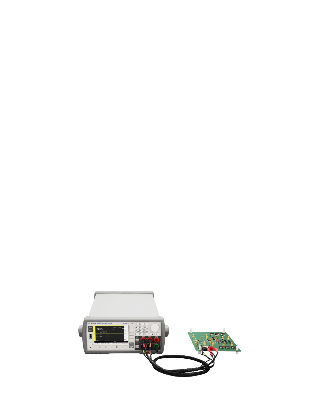
To avoid these troublesome tasks, you can use the Agilent B2961A/B2962A which provides
the programmable output resistance function. The B2961A/B2962A supports two operation
modes, constant and VI emulation, for this function. The constant mode lets the
B2961A/B2962A channel work as a voltage source with built-in constant series resistor (Rs) or
a current source with a built-in constant shunt resistor (Rsh). And the VI emulation mode lets
the channel work as a voltage source or current source with a built-in resistor which has a
non-linear I-V characteristics. By using this function, DC I-V characteristics of device/module
such as a battery can be emulated easily and effectively.
This document introduces the VI emulation mode of the programmable output resistance
function and the application examples by using the B2961A/B2962A. For the constant mode,
see another document “Using Constant Mode”, publication number B2960-90041.
)
4
Page 5
2. VI Emulation Mode
The VI emulation mode lets the B2961A/B2962A channel work as a source with a built-in
non-linear resistor. The channel can emulate an electronic devices or circuits which have a
non-linear four quadrant I-V characteristics. The characteristics is emulated by using the
impedance Z(I) which is a function of current and the admittance Y(V) which is a function of
voltage.
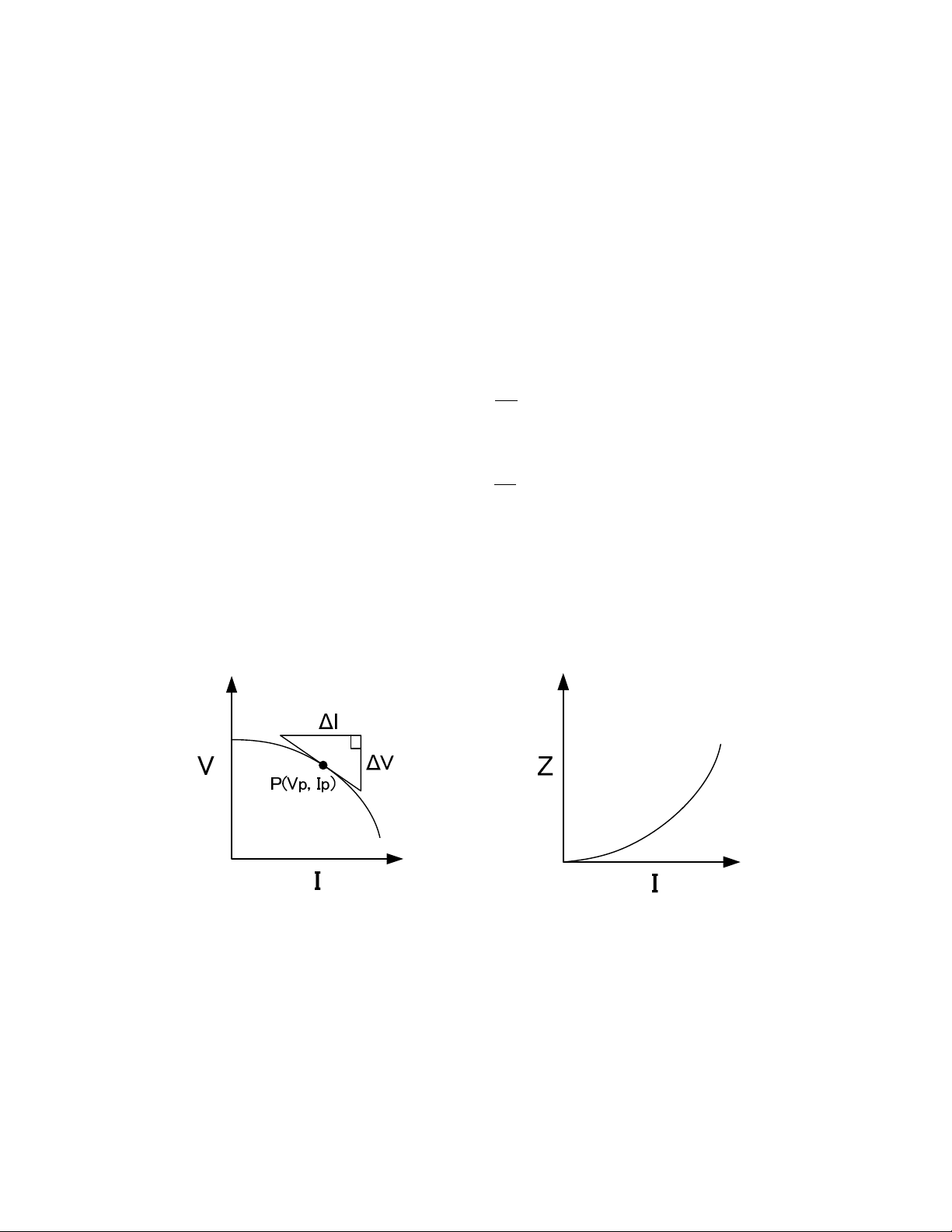
Simplified I-V characteristics of a battery cell is shown in Figure 1. When you draw a
tangent line at an operating point P in Figure 1 (a), its slope (ΔV/ΔI) is the impedance Z of
the device at the point P(Vp, Ip).
∆V
() =
∆I
And its reciprocal is the admittance Y.
∆I
() =
∆V
As shown above, Z and Y are the function of V or I. Using this fact, the I-V characteristics
is transformed into the Z-I (impedance-current) plane as shown in Figure 1 (b). Thus, the I-V
characteristics can be expressed by using the Z-I, V-Y, or their combination. For very high
impedance, conductance (Y) can be used. In this case, zero impedance (Z=0, Y=∞) gives the
constant voltage, and zero admittance (Y=0, Z=∞) gives the constant current.
(a)
Figure 1 I-V characteristics of a battery cell and its transformation function into Z-I plane
(b)
5
Page 6
Emulation table and PWL interpolation
The B2961A/B2962A uses a user defined emulation table and the piecewise linear (PWL)
interpolation to express a non-linear DC I-V characteristics. The emulation table is considered
as a data list which can store up to 16 pairs of voltage and current data. The PWL
interpolation is a widely used technique in engineering for approximating a complex function by
a simple (linear) function.
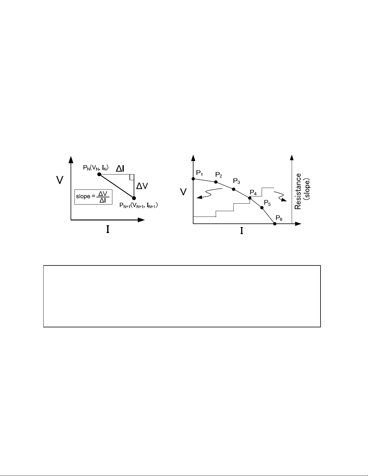
A pair of voltage and current data makes a point on the I-V plane as shown in Figure 2.
And the B2961A/B2962A channel performs the operation of the constant mode using the
resistance (Rs or Rsh) given by the slope between two adjacent points. Figure 3 shows an
example of I-V characteristics with six I-V data.
Figure 2 Emulation table data and slope
Figure 3 Example of I-V characteristics
Agilent B2961A/B2962A setting parameters:
Primary source mode (set to B2961A/B2962A front panel Mode): voltage (V) or current (I)
V and I source values (set to Output R (Emulation), emulation table)
V/I mode for transition between adjacent source values (set to Output R (Emulation),
emulation table)
Primary source mode and shape of I-V characteristics
Simplified block diagram of the B2961A/B2962A channel in the VI emulation mode is
shown in Figure 4. The upper part of the figure represents a voltage source with series
resistance (Rs) and the lower part represents a current source with shunt resistance (Rsh).
The channel initially works as a voltage source or a current source depending on the Mode
setting. This source mode is called as the primary source mode in this document. The
source mode for each transition between two adjacent points can be dynamically switched
according to the V/I mode set to the emulation table. By this mechanism, various shapes of
I-V characteristics can be emulated stably.
6
Page 7
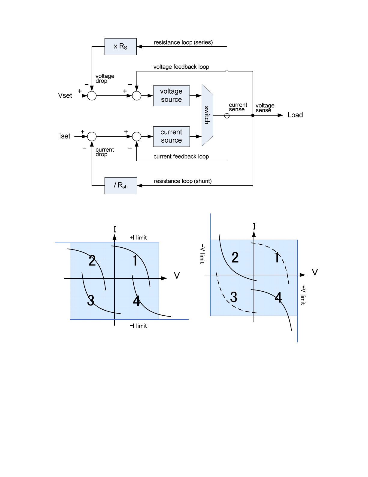
Figure 4 Simplified block diagram, VI emulation mode
(a) Primary source mode: Voltage (b) Primary source mode: Current
Figure 5 I-V shapes allowed in VI emulation mode
The shape of I-V characteristics to emulate must be classified into one of the patterns
shown in Figure 5. For example, a battery emulation described above is classified into the
pattern shown in the quadrant-1 of (a). And to emulate a lamp, the quadrant-4 of (a) should
be used. In this case, V is the B2961A/B2962A channel output voltage and I is the output
current. Positive current flows to load from channel.
7
Page 8
Note that the primary source mode must be specified before the programmable output
resistance function is enabled. Also, the primary source mode must be voltage for the I-V
characteristics like the quadrant-1 or 3.
V/I mode setting
The emulation table is used to set the voltage and current values for each point on the DC
I-V characteristics as described above. Also the table contains the V/I mode for each
transition between two adjacent points which is a necessary parameter to select the
B2961A/B2962A channel operation, voltage source or current source, most suitable for each
point and transition.
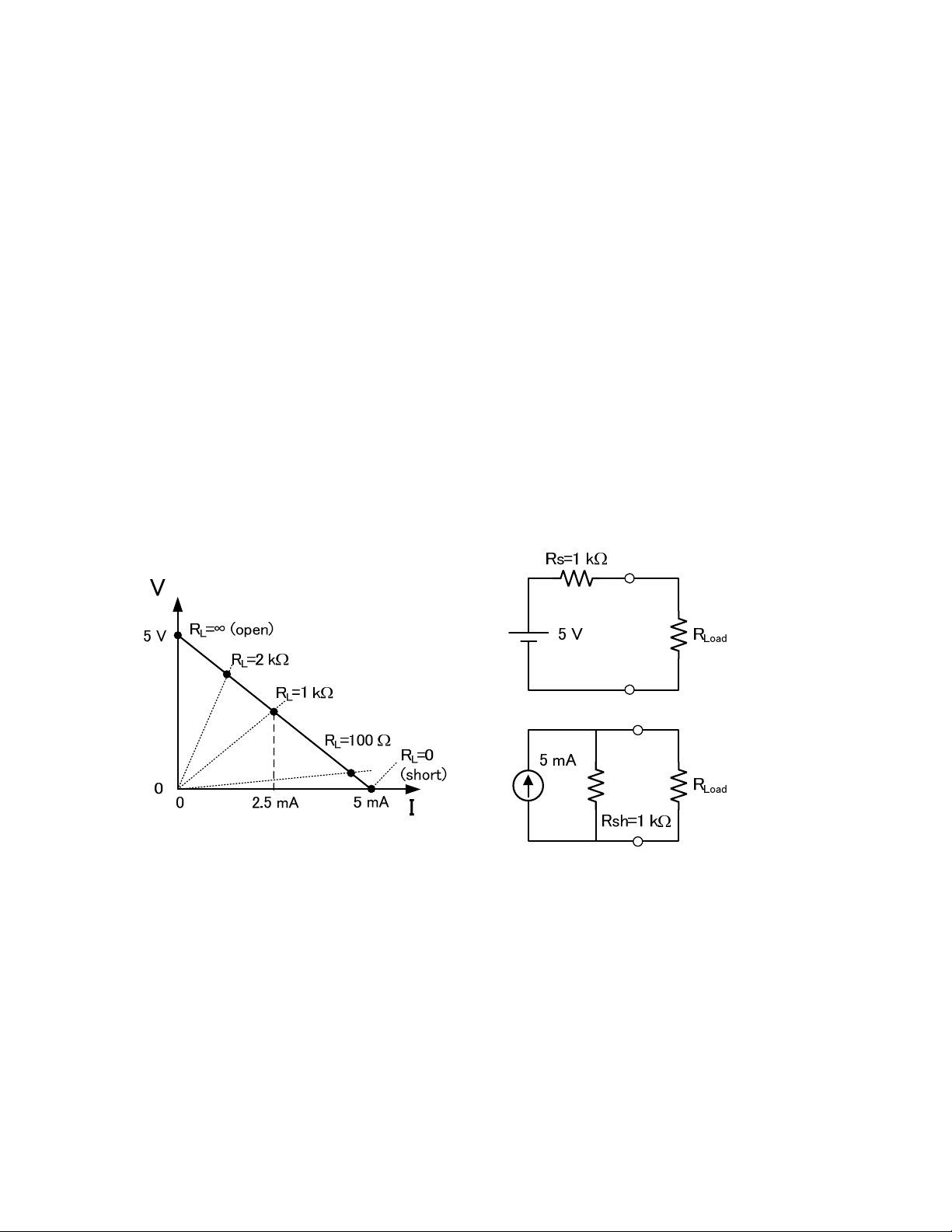
An example of I-V characteristics is shown in Figure 6. Theoretically, this characteristics
can be emulated by using either a 5 V voltage source with 1 kΩ series resistor or a 5 mA
current source with 1 kΩ shunt resistor as shown in Figure 7. However, it is difficult to
emulate the characteristics by using either of them due to the affect of the load resistance.
Generally, the voltage source is effective for R
R
Rsh.
Load
Figure 6 Linear I-V characteristics of Vopen=5 V
and Ishort=5 mA
Rs and the current source is effective for
Load
Figure 7 Two equivalent circuits to realize
characteristics shown in Figure 6
8
Page 9
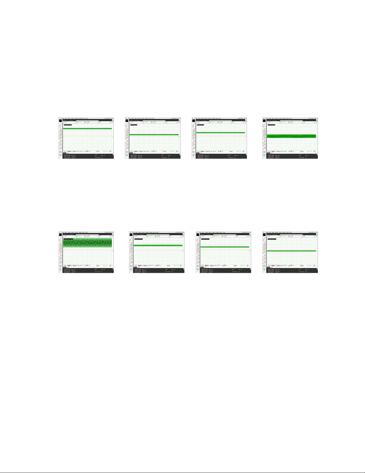
Figure 8 and Figure 9 show the load voltage measurement results of the above circuit (Figure
7) with several load resistors. The voltage source (V mode) works fine for R
output oscillates for R
for R
1 kΩ and its output starts oscillating over 2 kΩ. In this case, the critical load
Load
= 100 Ω. On the other hand, the current source (I mode) works fine
Load
1 kΩ, and its
Load
resistance value is 1 kΩ that is equal to Rs and Rsh. So the V/I mode should be switched at
this point which is actually not a point but a band with some width.
R
= 10 MΩ > Rs
Load
Stable
Figure 8 V mode operation with various R
R
= 2 kΩ > Rs
Load
Stable
R
= 1 kΩ = Rs
Load
Stable
Load
R
= 100 Ω < Rs
Load
Unstable
R
= 10 MΩ > Rsh
Load
R
= 2 kΩ > Rsh
Load
Unstable
Figure 9 I mode operation with various R
becoming Unstable
R
= 1 kΩ = Rsh
Load
Stable
Load
R
= 0.1 Ω < Rsh
Load
Stable
9
Page 10
Emulation table setting example
V
V
V
V
V
V
V
V
V
V
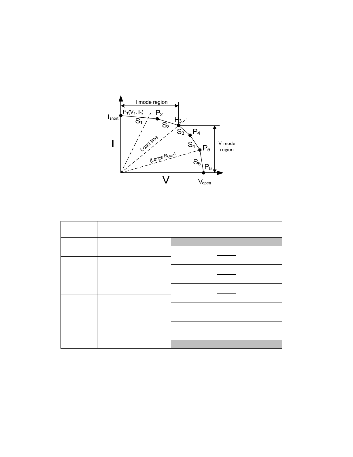
The I-V characteristics of a typical solar cell is shown in Figure 10. Dotted lines represent
load lines for several resistances. In this example, the I-V characteristics is split into 5 slopes,
S1 to S5. And the output resistance (S3) becomes the same as the load resistance at the
operating point P3. So the emulation table should be defined as shown in Table 1.
)
d
a
o
L
R
l
l
a
m
S
(
Figure 10 I-V characteristics of typical solar cell
Table 1 Voltage, Current, and V/I mode settings for above characteristics
Operating
point
Voltage Current Slope
Output
impedance
V/I mode
P1 (short) V1=0 I1
P2 V
P3 V
P4 V
P5 V
P6 (open) V6 I
I
2
I
3
I
4
I
5
6
2
3
4
5
=0
S1
S2
S3
S4
S5
−
I−I
−
I−I
−
I−I
−
I−I
−
I−I
I
I
V
V
V
Note that the system requires the descending order (from large value to small value) for the
Current column in the table.
This example assumes that the load capacitance is negligible and there is no internal bias
source in the load. If any bias source exists in the load, the load resistance looks different
and the V/I mode may need to be changed.
10
Page 11
Combination of V/I mode
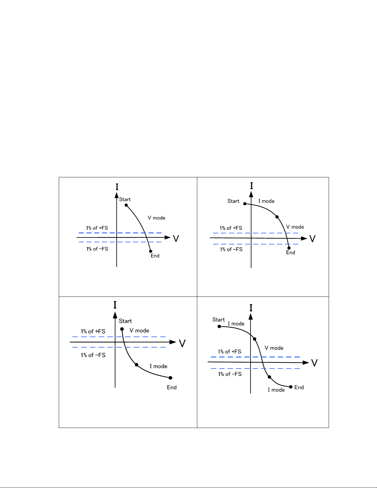
If the primary source mode is voltage
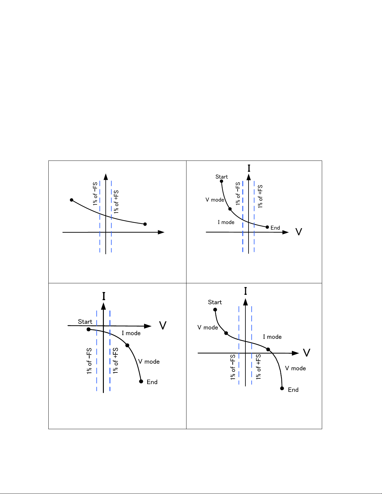
Combination of the V/I mode must be one of the following conditions (Figure 11).
(1) V mode only
(2) I mode (I > 0) to V mode
(3) V mode to I mode (I < 0)
(4) I mode (I > 0) to V mode to I mode (I < 0)
The I-V curve must be started by the positive current and ended by the negative current.
The I mode cannot be used within ±1 % of full scale of the current range (or ±10 % for the
10 nA range). So, the V mode must be used for this ±1 % region (or ±10 % region for the 10
nA range).
(1) V only
(3) V-I (4) I-V-I
Figure 11 V/I mode when the primary source mode is voltage
(2) I-V
11
Page 12
If the primary source mode is current
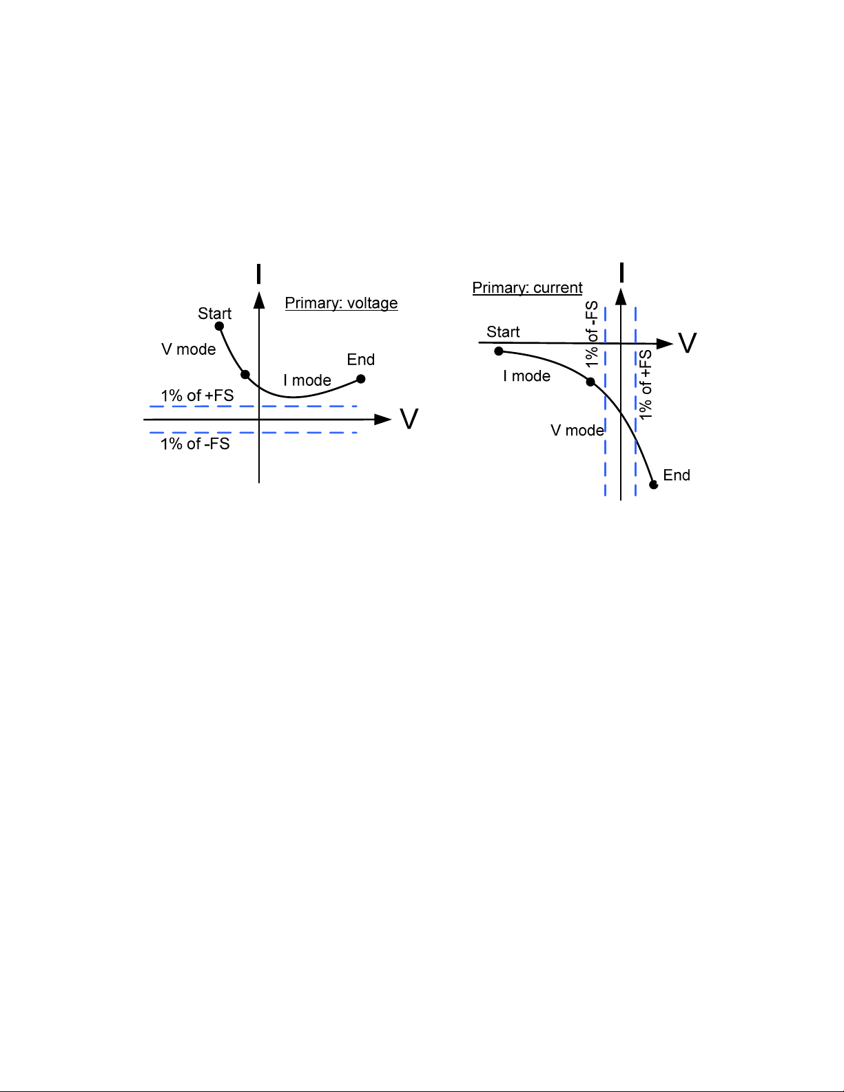
Combination of the V/I mode must be one of the following conditions (Figure 12).
(1) I mode only
(2) V mode (V < 0) to I mode
(3) I mode to V mode (V > 0)
(4) V mode (V < 0) to I mode to V mode (V > 0)
The I-V curve must be started by the negative voltage and ended by the positive voltage.
The V mode cannot be used within ±1 % of full scale of the voltage range (or ±10 % for the
200 mV range). So, the I mode must be used for this ±1 % region (or ±10 % region for the 200
mV range).
I
Start
I mode
(1) I only
End
V
(2) V-I
(3) I-V (4) V-I-V
Figure 12 V/I-mode when the primary source mode is current
12
Page 13
Bad examples
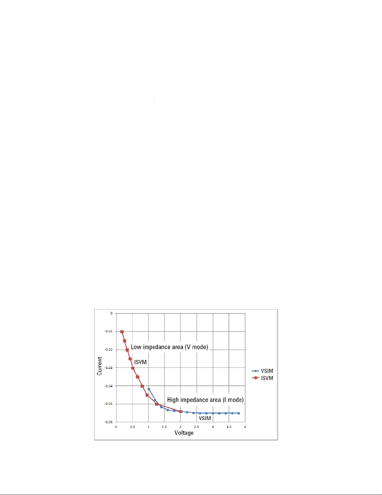
Bad examples of V/I mode combination are shown in Figure 13.
(a) is a bad example for the combination shown in Figure 11 (3). The positive current is not
allowed for the I mode, also the negative resistance (Rs or Rsh) is not allowed.
(b) is a bad example for the combination shown in Figure 12 (3). The V mode cannot be
used within ±1 % of full scale of the voltage range (or ±10 % for the 200 mV range).
(a)
Figure 13 Bad examples of V/I mode combination
(b)
Available Rs/Rsh values
See the document “Using Constant Mode”, publication number B2960-90041. The available
Rs/Rsh values for the constant mode are also effective for the VI emulation mode. However,
the negative resistance/conductance is not allowed for the VI emulation mode. So, the I-V
characteristics always shows the curve from upper left to lower right as shown in Figure 11
and Figure 12. Also, the shape of I-V characteristics is limited due to the internal
configuration as described above.
13
Page 14
Notes
t
r
t
A
u
h
o
s
u
e
I
s
t
s
e
n
n
n
t
o
m
e
o
o
The channel can be used for the
the load voltage or current.
The channel can be used betwee
emulation table. Do not apply v
The channel automatically selec
emulation table setting. They a
current values. Those ranges a
The channel output stability can
filter. However, this increases
Do not connect the other B2961
which uses the programmable o
When the channel works as a vo
undesirable noise increases. T
reduced by increasing the time c
For the setting error of Rs/Rsh,
number B2960-90041.
If you confirm the emulation res
DC emulation. It cannot respond to the fast tran
n the minimum value and the maximum value set
oltage/current outside this range to the channel.
s the voltage and current ranges according to the
re the smallest range that covers all voltage value
e fixed during source output.
be improved by increasing the time constant of th
he response time.
/B2962A channel in series or parallel to the chan
tput resistance function.
ltage source with high Rs and high current range,
is fundamental noise cannot be eliminated but ca
nstant of the output filter because it cuts off the
ee the document “Using Constant Mode”, publica
lt, use voltage source and current meter (VSIM) f
ition of
o the
or all
output
el
be
oise.
ion
r the
high impedance area (I mode) of
(ISVM) for the low impedance ar
for each measurement. Otherw
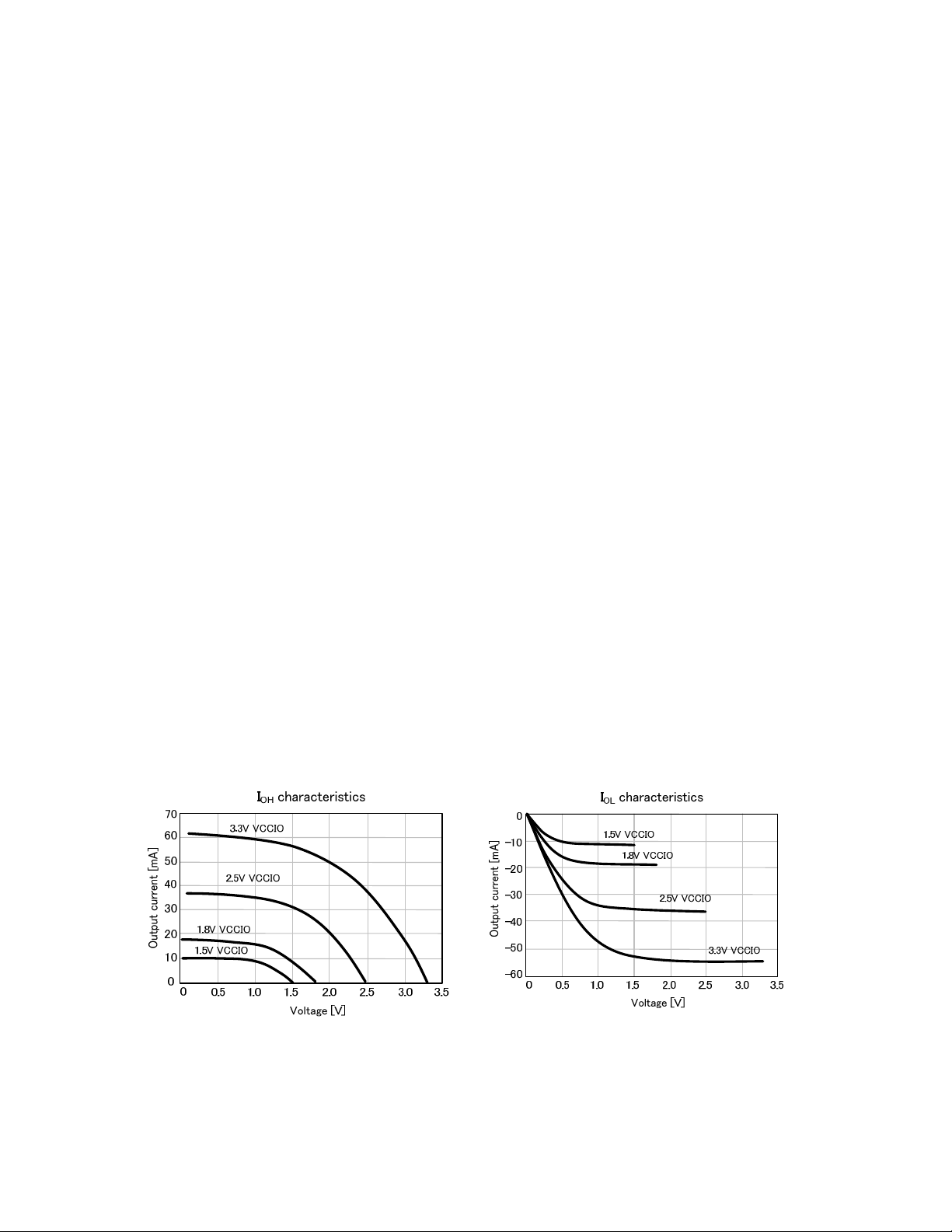
For example, as shown in the VS
monitored correctly by VSIM. S
correctly by ISVM.
the VI emulation and use current source and volt
a (V mode). Most suitable instrument should b
ise, the emulation result cannot be monitored corr
M line of Figure 14, the low impedance area cann
imilarly, the high impedance area cannot be monit
eter
used
ectly.
t be
red
Figure 14 VI emulation result measured
by external instruments
14
Page 15
3. Application
Agilent B2961A/B2962A Power Source can be a voltage source or a current source which
enables wide range voltage/current output and advanced test and evaluation. And its
programmable output resistance function is effective for several applications such as error
compensation, source emulation, resistance emulation, and so on. This section introduces
the following examples for using this function.
To emulate an I/O driver circuit of logic IC
To emulate a solar cell
To emulate an I/O driver circuit of logic IC
Introduction
I-V characteristics (IOH: Logic-High level output current, IOL: Logic-Low level input current) of
a logic IC driver circuit are shown in Figure 15. They are typical characteristics which you can
obtain from an IC data sheet or an IBIS (Input/Output Buffer Information Specification) model
file if available. As shown in the graph, the output resistance of the driver circuit is not linear.
And the characteristics are affected by the operating conditions such as applied voltage,
temperature, and so on.
For designing a device, a module, or a circuit which receives the driver output, it is important
to check its operation with several variations of driver outputs. However it is difficult and
inefficient to prepare several driver circuits or to realize several operating conditions. Then,
the VI emulation by using the B2961A/B2962A is an effective solution to obtain the various
outputs easily.
(a) I
(b) IOL
OH
Figure 15 I-V characteristics of a driver circuit (IOH and IOL) for various power supply (VCCIO)
15
Page 16
t
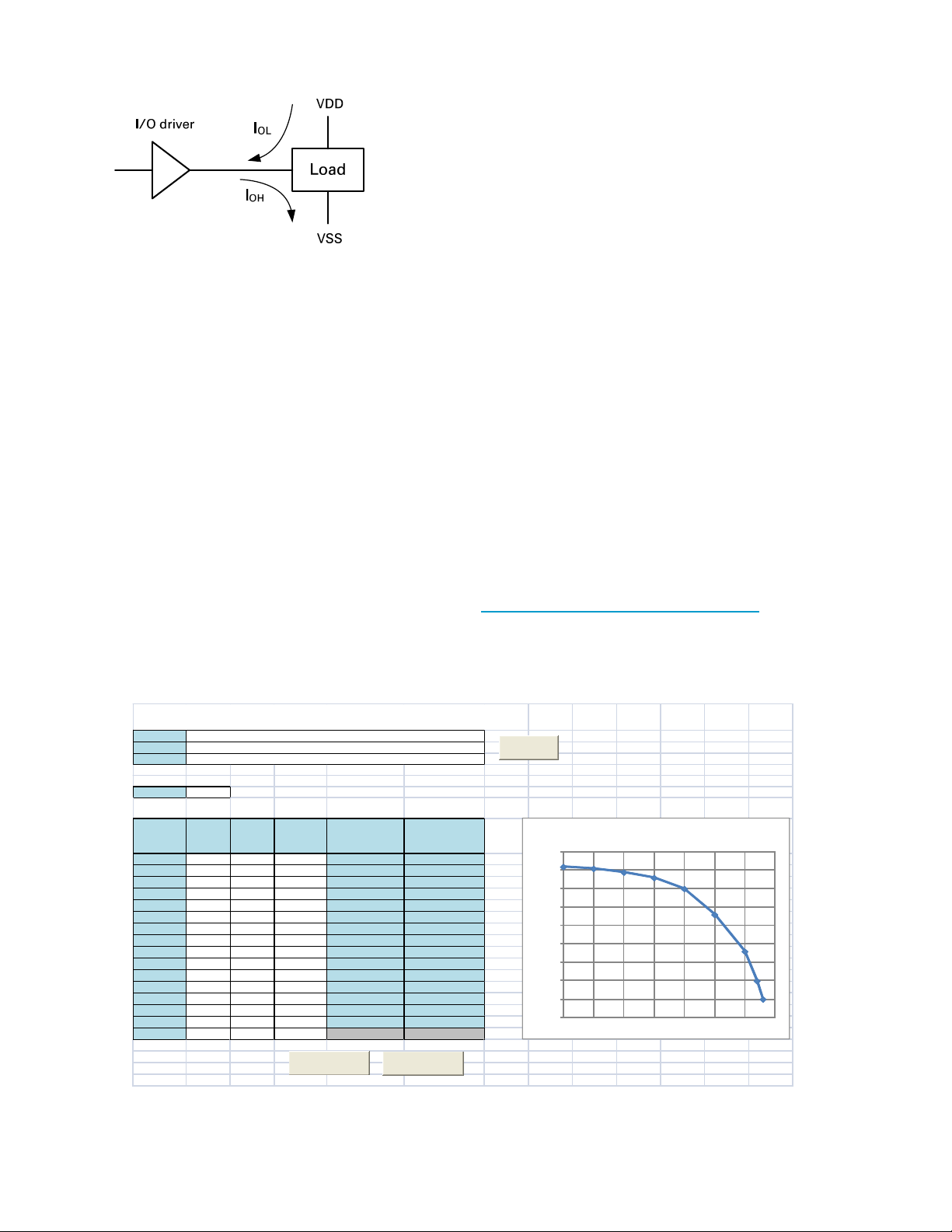
Figure 16 Current flow between I/O driver and load
Emulation example
The following example is for the IOH emulation of 3.3 volts VCCIO. The settings of the
B2961A/B2962A are shown below. For this emulation, the primary source mode must be
voltage because the shape is similar to the pattern of the quadrant-1 shown in Figure 5 (a).
Primary source mode (B2961A/B2962A front panel Mode setting): voltage (V)
V and I source values (in emulation table): See Voltage and Current columns in Figure 17.
V/I mode (in emulation table): See Mode column in Figure 17.
Figure 17 shows the setup image when the VI Emulation Sample Program is used. The
program is available from Agilent B2900 web site (http://www.agilent.com/find/b2900a).
This program automatically calculates the output resistance and conductance, and displays the
I-V characteristics.
B2961A/B 2962A VI Emulat ion Sample Program, R ev. 1.2, 2012/9/25
ADDRESS
TIMEOUT
*IDN?
Primary Voltage(0)
Voltage
Index
0 0 62 I 500 0.002
1 0.5 61 I 250 0.004
2 1 59 I 166.6666667 0.006
3 1.5 56 I 83.33333333 0.012
4 2 50 V 35.71428571 0.028
5 2.5 36 V 25 0.04
6 3 16 V 12.5 0.08
73.20 V 10 0.1
83.3-10
9
10
11
12
13
14
15
Current
[V]
[mA]
UsbInstrument1
Mode
V(0), I(1)
3000
*IDN?
Output resistance
(slope) [V/I]
Se
Output
conductance
(1/slope) [I/V]
Disable
Connect
V-I characteristics
70
60
50
40
30
20
CUrrent [mA]
10
0
0 0 .5 1 1.5 2 2 .5 3 3.5
-10
-20
Voltage [V]
Figure 17 B2961A/B2962A VI Emulation Sample Program settings for IOH emulation
16
Page 17
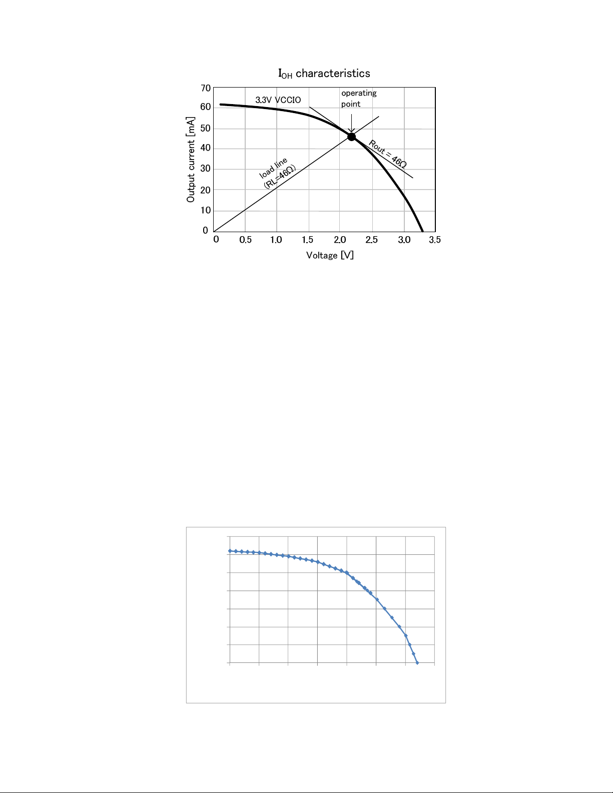
Figure 18 Load line for selecting V/I mode
The V and I source values can be selected by reading the values on the curve shown in
Figure 18. This example assumes that the load does not have internal bias and the load line
starts from the origin.
The V/I mode should be selected after finding the point which satisfies R
According to Figure 18, this point is on the 46 Ω load line. So, I mode should be used for R
46 Ω, and V mode should be used for R
46 Ω. Depending on the emulation result, you
Load
= Rs = Rsh.
Load
Load
may need to adjust the setting.
Figure 19 shows the emulation result. The result can be monitored by using an external
instrument. Then use voltage source and current meter (VSIM) for the high impedance area (I
mode) of the VI emulation, and use current source and volt meter (ISVM) for the low
impedance area (V mode).
0.07
0.06
0.05
0.04
0.03
Cu rrent [A]
0.02
0.01
0
00.511.522.533.5
Voltage [V]
Figure 19 IOH characteristics emulation result measured by external instruments
17
Page 18
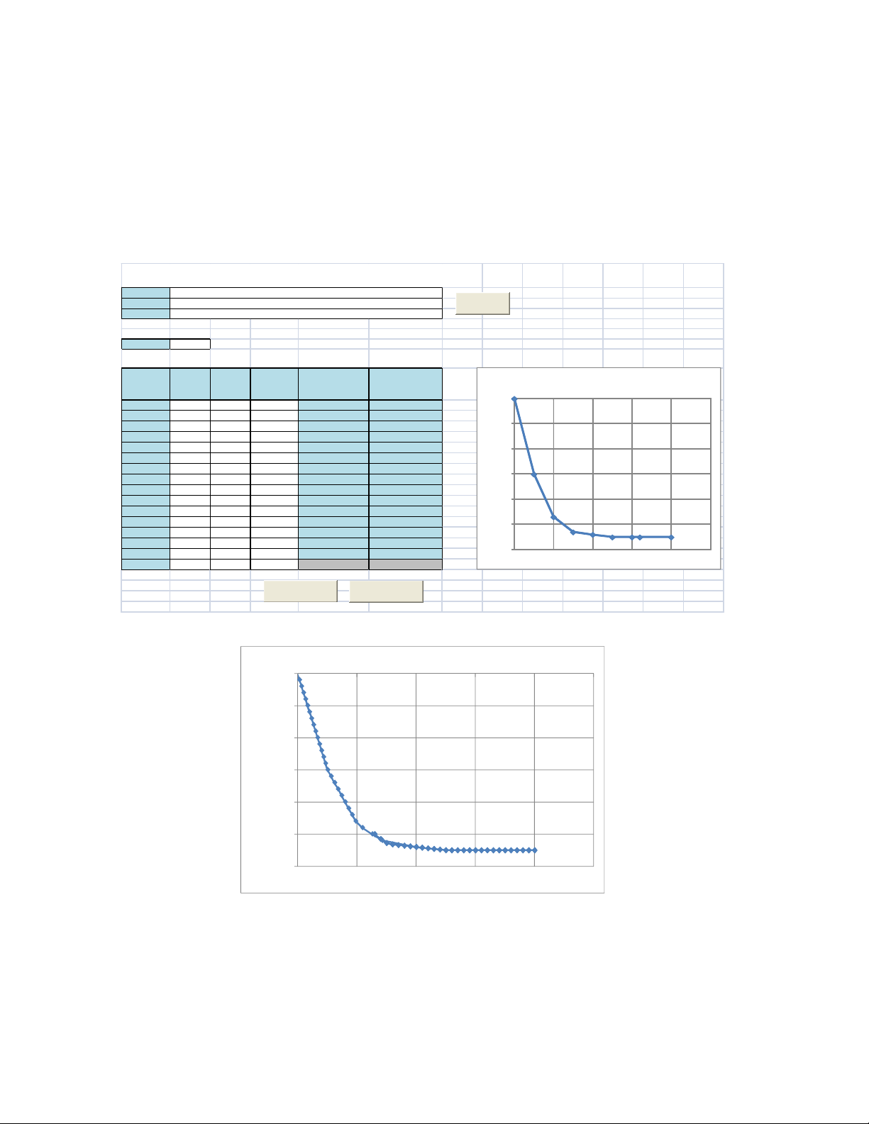
The following example is for the IOL emulation of the same device. For this emulation, the
t
primary source mode must be voltage because the shape is similar to the pattern of the
quadrant-4 shown in Figure 5 (a).
Primary source mode (B2961A/B2962A front panel Mode setting): voltage (V)
V and I source values (in emulation table): See Voltage and Current columns in Figure 20.
V/I mode (in emulation table): See Mode column in Figure 20.
B2961A/B 2962A VI Emulat ion Sample Program, R ev. 1.2, 2012/9/25
ADDRESS
TIMEOUT
*IDN?
Primary Voltage(0)
UsbInstrument1
3000
*IDN?
Connect
Voltage
Index
0 0 0 V 16.66666667 0.06
1 0.5 -30 V 29.41176471 0.034
2 1 -47 V 83.33333333 0.012
3 1.5 -53 I 500 0.002
4 2 -54 I 500 0.002
52.5-55I inf 0
63-55I inf 0
73.2-55I inf 0
84-55
9
10
11
12
13
14
15
Current
[V]
[mA]
Mode
V(0), I(1)
Output resistance
(slope) [V/I]
Se
Output
conductance
(1/slope) [I/V]
Disable
V-I characteristics
0
012345
-10
-20
-30
CUrrent [mA]
-40
-50
-60
Voltage [V]
Figure 20 B2961A/B2962A VI Emulation Sample Program settings for IOL emulation
012345
0
-0.01
-0.02
-0.03
Current [A]
-0.04
-0.05
-0.06
Vo ltage [V]
Figure 21 IOL characteristics emulation result measured by external instruments
As described above, two characteristics of a logic IC driver circuit are emulated easily by
using the B2961A/B2962A. Special setup for the VI emulation is the emulation table only.
Just by filling the table with appropriate V and I values, the B2961A/B2962A can emulate
various DC output characteristics.
18
Page 19
To emulate a solar cell
Introduction
Solar cell is attractive device as it is a sustainable energy source, and has been used for
wide applications, for example, portable devices or remote sensing units, and such. Output
I-V characteristics of solar cell is affected by the operating conditions such as light power,
temperature, and so on. Aging and the stain on the surface also affect the performance.
For designing a device, a module, or a circuit which uses solar cell as power source, it is
important to check its operation in several operating conditions. However it is difficult and
inefficient to use actual solar cell or to realize several operating conditions. Then, the VI
emulation is an effective solution to obtain the various power conditions easily.
Emulation example
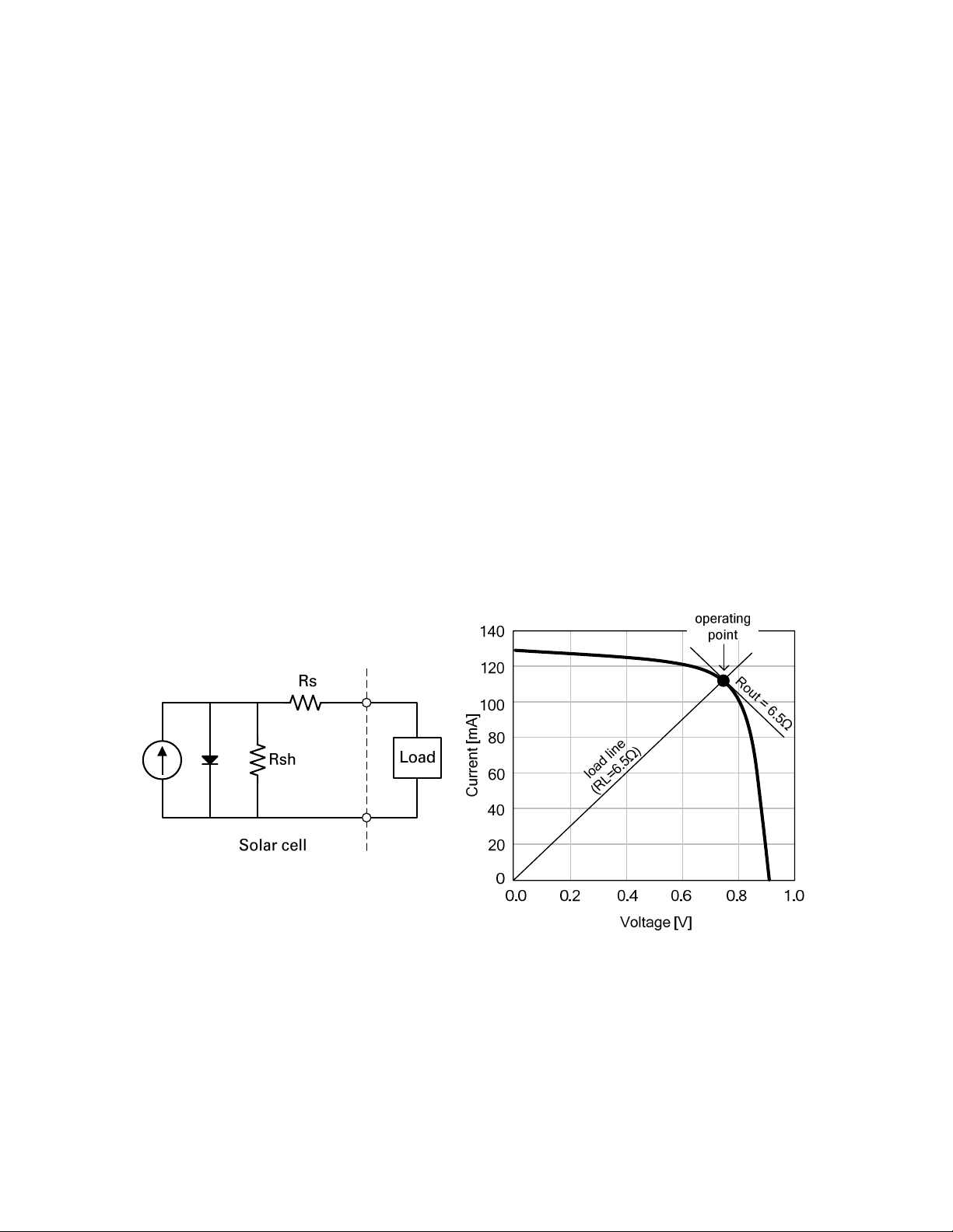
Simplified equivalent circuit of solar cell is shown in Figure 22. It consists of the ideal
current source, a diode, a shunt resistor (Rsh), and a series resistor (Rs) which contains
internal series resistor and external wire resistance. Generally, Rsh causes leakage current,
and Rs causes voltage drop depending on load current.
Figure 22 Simplified equivalent circuit of
solar cell
Figure 23 I-V characteristics of solar cell to emulate
Figure 23 shows I-V characteristics of a solar cell. This output characteristics can be
emulated by the following setup.
Primary source mode (B2961A/B2962A front panel Mode setting): voltage (V)
V and I source values (in emulation table): See Voltage and Current columns in Figure 24.
V/I mode (in emulation table): See Mode column in Figure 24.
19
Page 20
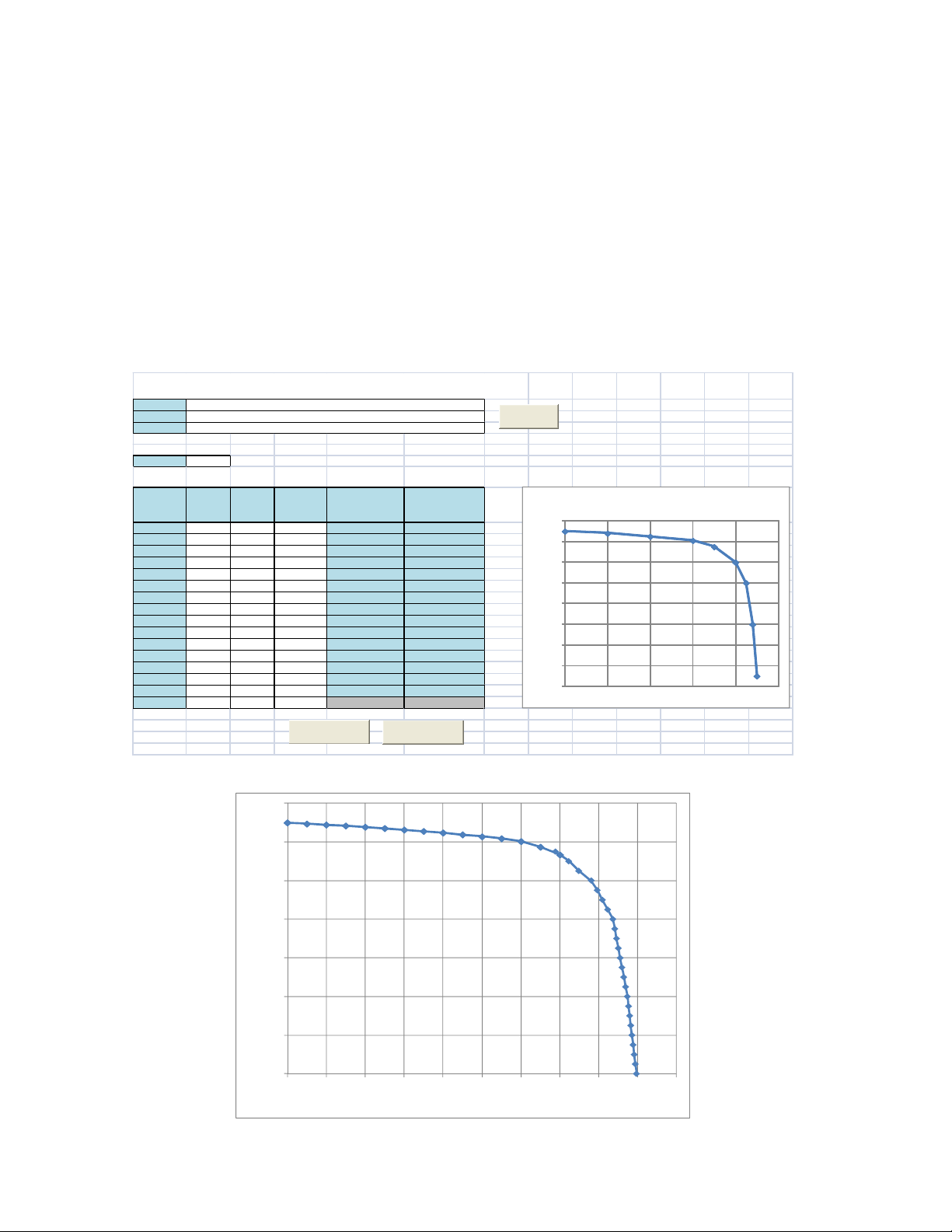
The primary source mode must be voltage because the shape is similar to the pattern of the
t
quadrant-1 shown in Figure 5 (a).
The V and I source values can be selected by reading the curve shown in Figure 23. The
values can be also selected from calculation or simulation like SPICE for emulating the output
characteristics in the several temperature conditions, various darkness conditions, and such.
The V/I mode should be selected after finding the point which satisfies R
= Rs = Rsh.
Load
According to Figure 23, this point is on the 6.5 Ω load line. So, I mode should be used for R
6.5 Ω, and V mode should be used for R
6.5 Ω. Emulation result is shown in Figure 25.
Load
Depending on the emulation result, you may need to adjust the setting.
B2961A/B 2962A VI Emulat ion Sample Program, R ev. 1.2, 2012/9/25
ADDRESS
TIMEOUT
*IDN?
Primary Voltage(0)
Voltage
Index
00130I 100 0.01
1 0.2 128 I 66.66666667 0.015
2 0.4 125 I 50 0.02
3 0.6 121 I 16.66666667 0.06
4 0.7 115 I 6.666666667 0.15
5 0.8 100 V 2.5 0.4
6 0.85 80 V 0.75 1.333333333
7 0.88 40 V 0.4 2.5
80.9-10
9
10
11
12
13
14
15
Current
[V]
[mA]
UsbInstrument1
Mode
V(0), I(1)
3000
*IDN?
Output resistance
(slope) [V/I]
Output
conductance
(1/slope) [I/V]
Connect
V-I characteristics
140
120
100
80
60
CUrrent [mA]
40
20
0
0 0.2 0.4 0.6 0.8 1
-20
Voltage [V]
Load
Se
Disable
Figure 24 B2961A/B2962A VI Emulation Sample Program settings for solar cell
0.14
0.12
0.1
0.08
Current
0.06
0.04
0.02
0
0 0.10.20.30.40.50.60.70.80.9 1
Voltage
Figure 25 Solar cell I-V characteristics emulation result measured by external instruments
20
Loading...