

Page 1

Technical Specifications
Agilent Technologies
PNA Series Network Analyzers
N5242A
Options 200/219/224 (2-Port PNA-X)
Options 400/419/423 (4-Port PNA-X)
Manufacturing Part Number: N5242-90007
Printed in USA
Print Date: September 6, 2007
Supersedes: July 17, 2007
© Copyright © Agilent Technologies, Inc. 2007 All rights reserved.
Page 2

Documentation Warranty
THE MATERIAL CONTAINED IN THIS DOCUMENT IS PROVIDED "AS IS," AND IS
SUBJECT TO BEING CHANGED, WITHOUT NOTICE, IN FUTURE EDITIONS. FURTHER, TO THE MAXIMUM EXTENT PERMITTED BY APPLICABLE LAW, AGILENT
DISCLAIMS ALL WARRANTIES, EITHER EXPRESS OR IMPLIED WITH REGARD TO
THIS MANUAL AND ANY INFORMATION CONTAINED HEREIN, INCLUDING BUT
NOT LIMITED TO THE IMPLIED WARRANTIES OF MERCHANTABILITY AND FITNESS FOR A PARTICULAR PURPOSE. AGILENT SHALL NOT BE LIABLE FOR
ERRORS OR FOR INCIDENTAL OR CONSEQUENTIAL DAMAGES IN CONNECTION
WITH THE FURNISHING, USE, OR PERFORMANCE OF THIS DOCUMENT OR ANY
INFORMATION CONTAINED HEREIN. SHOULD AGILENT AND THE USER HAVE A
SEPARATE WRITTEN AGREEMENT WITH WARRANTY TERMS COVERING THE
MATERIAL IN THIS DOCUMENT THAT CONFLICT WITH THESE TERMS, THE WARRANTY TERMS IN THE SEPARATE AGREEMENT WILL CONTROL.
DFARS/Restricted Rights Notice
If software is for use in the performance of a U.S. Government prime contract or
subcontract, Software is delivered and licensed as “Commercial computer software” as
defined in DFAR 252.227-7014 (June 1995), or as a “commercial item” as defined in FAR
2.101(a) or as “Restricted computer software” as defined in FAR 52.227-19 (June 1987) or
any equivalent agency regulation or contract clause. Use, duplication or disclosure of
Software is subject to Agilent Technologies’ standard commercial license terms, and
non-DOD Departments and Agencies of the U.S. Government will receive no greater than
Restricted Rights as defined in FAR 52.227-19(c)(1-2) (June 1987). U.S. Government users
will receive no greater than Limited Rights as defined in FAR 52.227-14 (June 1987) or
DFAR 252.227-7015 (b)(2) (November 1995), as applicable in any technical data.
Printing Copies of Documentation from the Web
To print copies of documentation from the Web, download the PDF file from the Agilent
web site:
•Go to www.agilent.com.
• Enter the product model number in the search function and click Search.
• Click on the Manuals hyperlink.
• Open the PDF of your choice and print the document .
Page 3

Contacting Agilent
Assistance with test and measurement needs and information on finding a local Agilent
office are available on the Web at:
www.agilent.com/find/assist
If you do not have access to the Internet, please contact your Agilent field engineer.
NOTE
In any correspondence or telephone conversation, refer to the Agilent product
by its model number and full serial number. With this information, the
Agilent representative can determine whether your product is still within its
warranty period.
Page 4

This page intentionally left blank.
Page 5

Documentation Warranty
THE MATERIAL CONTAINED IN THIS DOCUMENT IS PROVIDED "AS IS," AND IS SUBJECT
TO BEING CHANGED, WITHOUT NOTICE, IN FUTURE EDITIONS. FURTHER, TO THE
MAXIMUM EXTENT PERMITTED BY APPLICABLE LAW, AGILENT DISCLAIMS ALL
WARRANTIES, EITHER EXPRESS OR IMPLIED WITH REGARD TO THIS MANUAL AND ANY
INFORMATION CONTAINED HEREIN, INCLUDING BUT NOT LIMITED TO THE IMPLIED
WARRANTIES OF MERCHANTABILITY AND FITNESS FOR A PARTICULAR PURPOSE.
AGILENT SHALL NOT BE LIABLE FOR ERRORS OR FOR INCIDENTAL OR
CONSEQUENTIAL DAMAGES IN CONNECTION WITH THE FURNISHING, USE, OR
PERFORMANCE OF THIS DOCUMENT OR ANY INFORMATION CONTAINED HEREIN.
SHOULD AGILENT AND THE USER HAVE A SEPARATE WRITTEN AGREEMENT WITH
WARRANTY TERMS COVERING THE MATERIAL IN THIS DOCUMENT THAT CONFLICT
WITH THESE TERMS, THE WARRANTY TERMS IN THE SEPARATE AGREEMENT WILL
CONTROL.
DFARS/Restricted Rights Notice
If software is for use in the performance of a U.S. Government prime contract or subcontract,
Software is delivered and licensed as “Commercial computer software” as defined in DFAR
252.227-7014 (June 1995), or as a “commercial item” as defined in FAR 2.101(a) or as
“Restricted computer software” as defined in FAR 52.227-19 (June 1987) or any equivalent
agency regulation or contract clause. Use, duplication or disclosure of Software is subject to
Agilent Technologies’ standard commercial license terms, and non-DOD Departments and
Agencies of the U.S. Government will receive no greater than Restricted Rights as defined in
FAR 52.227-19(c)(1-2) (June 1987). U.S. Government users will receive no greater than Limited
Rights as defined in FAR 52.227-14 (June 1987) or DFAR 252.227-7015 (b)(2) (November 1995),
as applicable in any technical data.
Page 6

Definitions ............................................................................................ 4
Corrected System Performance......................................................... 5
Table 1a. System Dynamic Range at Test Port 1.......................................5
Table 1b. System Dynamic Range at Test Port 1.......................................6
Table 1c. System Dynamic Range at Test Port 1........................................7
Table 1d. System Dynamic Range at Test Port 1.......................................8
Table 2a Extended Dynamic Range at Direct Receiver Access Input1......9
Table 2b. Extended Dynamic Range at Direct Receiver Access Input1...10
Table 2c. Extended Dynamic Range at Direct Receiver Access Input1....11
Table 2d. Extended Dynamic Range at Direct Receiver Access Input1...12
N5242A Corrected System Performance with 3.5mm Connectors...........13
Table 3. 85052B Calibration Kit N5242A..................................................13
Table 4. N4433A 4-Port Electronic Calibration Module N5242A..............16
Table 5. N4691B 2- Port Electronic Calibration Module...........................19
Uncorrected System Performance .................................................. 22
Table 6. Error Terms1...............................................................................22
Test Port Output.......................................................................................25
Table 7. Frequency Information ...............................................................25
Table 8a. Maximum Leveled Power.........................................................25
Table 8b. Maximum Leveled Power.........................................................30
Table 8c. Maximum Leveled Power .........................................................31
Table 8d. Maximum Leveled Power.........................................................32
Table 8e. Maximum Leveled Power.........................................................33
Table 8f. Maximum Leveled Power..........................................................34
Table 9a. Power Level Accuracy..............................................................35
Table 9b. Power Level Linearity...............................................................36
Table 9c. (Continued) Power Level Linearity............................................36
Table 9d. Power Level Linearity...............................................................37
Table 10a. Power Sweep Range..............................................................37
Table 10b. Power Sweep Range..............................................................38
Table 10c. Power Sweep Range..............................................................38
Table 10d. Power Sweep Range..............................................................39
Table 11. Nominal Power (Preset Power)................................................39
Table 12. Power Resolution and Maximum/Minimum Settable Power.....40
Table 13. Harmonics at Max Specified Power..........................................41
Table 14. Non-Harmonic Spurs at nominal power....................................42
Table 15. Phase Noise.............................................................................43
Test Port Input ................................................................................... 44
Table 16. Test Port Input ................................................................... 44
2
Page 7

Dynamic Accuracy ............................................................................ 50
Table 17 Dynamic Accuracy (Specification)............................................. 50
Table 18. Test Port Input (Group Delay)a.................................................57
General Information .......................................................................... 58
Table 19. Miscellaneous Information........................................................58
Table 20. Front Panel Information............................................................58
Table 21 Rear Panel Information .............................................................60
Table 22. Analyzer Dimensions and Weight.............................................65
Measurement Throughput Summary............................................... 66
Table 23. Typical Cycle Timea (ms) for Measurement Completion ..........66
Table 24. Cycle Time vs IF Bandwidth.....................................................68
Table 25. Cycle Time vs Number of Points..............................................69
Table 26. Data Transfer Time (ms) ..........................................................71
Specifications: Front-Panel Jumpers .............................................. 72
Table 27 Measurement Receiver Inputs ..................................................73
Table 28. Reference Receiver Input.........................................................74
Table 29. Reference Receiver Input.........................................................75
Table 30. Reference Output.....................................................................77
Table 31. Reference Output.....................................................................78
Table 32. Source Outputs........................................................................80
Table 33. Coupler Inputs..........................................................................82
Test Set Block Diagrams .................................................................. 83
3
Page 8

This is a complete list of the technical specifications for the N5242A PNA-X network analyzer with
the following options:
Option 200, 2-port standard test set (includes six front-panel access loops) and power range.
See the block diagram
Option 219, adds 2-port extended power range, source and receiver attenuators, and bias-tees
(requires Option 200). See the block diagram
Option 224, adds an internal second source, a combiner, and mechanical switches to the 2-port
analyzer (requires Option 200, 219, and 080). See the block diagram
Option 400, 4-port standard test set (includes twelve front-panel access loops), power range, and
an internal second source (Option 080 recommended). See the block diagram
Option 419, adds 4-port extended power range, source and receiver attenuators, and bias-tees
(requires Option 400). See the block diagram
Option 423, adds an internal combiner, and mechanical switches to the 4-port analyzer (requires
Option 400, 419, and 080). See the block diagram
Note
This document provides technical specifications for the 85052B calibration kit, the N4433A 4-Port
ECal module, and the N4691B 2-Port ECal module. Please download our free Uncertainty
Calculator from http://www.agilent.com/find/na_calculator to generate the curves for your
calibration kit and PNA setup.
.
.
.
.
.
.
Definitions
All specifications and characteristics apply over a 25 °C ±5 °C range (unless otherwise stated)
and 90 minutes after the instrument has been turned on.
Specification (spec.): Warranted performance. Specifications include guardbands to account for
the expected statistical performance distribution, measurement uncertainties, and changes in
performance due to environmental conditions.
Characteristic (char.): A performance parameter that the product is expected to meet before it
leaves the factory, but that is not verified in the field and is not covered by the product warranty. A
characteristic includes the same guardbands as a specification.
Typical (typ.): Expected performance of an average unit which does not include guardbands. It is
not covered by the product warranty.
Nominal (nom.): A general, descriptive term that does not imply a level of performance. It is not
covered by the product warranty.
Calibration: The process of measuring known standards to characterize a network analyzer's
systematic (repeatable) errors.
Corrected (residual): Indicates performance after error correction (calibration). It is determined
by the quality of calibration s tandards and ho w well "known" they are, plus system repeatabili t y,
stability, and noise.
Uncorrected (raw): Indicates instrument performance without error correction. The uncorrected
performance affects the stability of a calibration.
Standard: When referring to the analyzer, this includes no options unless noted otherwise.
4
Page 9

Corrected System Performance
The specifications in this section apply for measurements made with the N5242A analyzer with
the following conditions:
• 10 Hz IF bandwidth
• No averaging applied to data
• Isolation calibration with an averaging factor of 8
Table 1a. System Dynamic Range at Test Port
1
Option 200 or 400
Description Specification (dB) at Test Port Typical (dB) at Test Port
Port 1 or 32 Port 2 or 42 Port 1 or 32 Port 2 or 42
10 MHz to 50 MHz3 93 93 106 104
50 MHz to 100 MHz3 103 103 116 115
100 MHz to 500 MHz3 117 117 131 130
500 MHz to 3.2 GHz 124 127 130 135
3.2 GHz to 10 GHz 127 127 137 136
10 GHz to 16 GHz 127 127 134 133
16 GHz to 20 GHz 127 124 133 129
20 GHz to 24 GHz 122 117 130 126
24 GHz to 26.5 GHz 112 109 124 120
1. The system dynamic range is calculated as the difference between the noise floor and the
specified source maximum output power. The effective dynamic range must take
measurement uncertainties and interfering signals into account.
2. Either port can be used as the source port. Any other port can be used as the receiver port.
3. May typically be degraded at particular frequencies below 500 MHz due to spurious receiver
residuals.
5
Page 10

Table 1b. System Dynamic Range at Test Port
1
Option 219 or 419
Description Specification (dB) at Test Port Typical (dB) at Test Port
Port 1 or
2
3
Port 2 or 4
2
Port 1 or 32 Port 2 or 42
10 MHz to 50 MHz3 93 93 106 104
50 MHz to 100 MHz3 103 103 115 114
100 MHz to 500 MHz3 117 117 130 129
500 MHz to 3.2 GHz 124 127 130 135
3.2 GHz to 10 GHz 127 127 135 134
10 GHz to 16 GHz 126 125 132 131
16 GHz to 20 GHz 124 122 130 127
20 GHz to 24 GHz 118 117 127 124
24 GHz to 26.5 GHz 110 106 121 117
1
The system dynamic range is calculated as the difference between the noise floor and the
specified source maximum output power. The effective dynamic range must take measurement
uncertainties and interfering signals into account.
2
Either port can be used as the source port. Any other port can be used as the receiver port.
3
May typically be degraded at particular frequencies below 500 MHz due to spurious receiver
residuals.
6
Page 11

Table 1c. System Dynamic Range at Test Port
1
Option 224
Description Specification (dB) at Test Port Typical (dB) at Test Port
Source 2,
Out 1
Source 2,
Out 2
Source 2,
Out 1
Source 2,
Out 2
10 MHz to 50 MHz2 98 93 108 105
50 MHz to 100 MHz2 108 107 117 116
100 MHz to 500 MHz2 122 121 132 131
500 MHz to 3.2 GHz 128 128 134 136
3.2 GHz to 10 GHz 132 132 139 139
10 GHz to 16 GHz 130 130 138 137
16 GHz to 20 GHz 129 127 136 134
20 GHz to 24 GHz 123 122 133 132
24 GHz to 26.5 GHz 114 112 127 124
1
The system dynamic range is calculated as the difference between the noise floor and the
specified source maximum output power. The effective dynamic range must take measurement
uncertainties and interfering signals into account.
2
May typically be degraded at particular frequencies below 500 MHz due to spurious receiver
residuals.
7
Page 12

Table 1d. System Dynamic Range at Test Port
Option 224 or 423
1
Description Specification
Typical (dB) at Test Port
(dB) at Test Port
Port 1
or 3
Port 2
2
or 42
Port 1
or 32
Port 2
or 42
Source 1, Port
1 Combine
Mode
Source 2, Port
1 Combine
Mode
10 MHz to 50 MHz3 93 93 106 104 104 80
50 MHz to 100
3
MHz
100 MHz to 500
3
MHz
103 103 115 115 112 90
117 117 130 130 121 99
500 MHz to 3.2 GHz 124 127 130 134 127 112
3.2 GHz to 10 GHz 127 127 136 134 132 119
10 GHz to 16 GHz 126 124 132 131 128 115
16 GHz to 20 GHz 124 121 130 127 125 113
20 GHz to 24 GHz 117 115 127 124 121 109
24 GHz to 26.5 GHz 107 105 121 117 115 102
1
The system dynamic range is calculated as the difference between the noise floor and the
specified source maximum output power. The effective dynamic range must take measurement
uncertainties and interfering signals into account.
2
Either port can be used as the source port. Any other port can be used as the receiver port.
3
May typically be degraded at particular frequencies below 500 MHz due to spurious receiver
residuals.
8
Page 13

1
Table 2a Extended Dynamic Range at Direct Receiver Access Input
Option 200 or 400
Description Typical (dB) at Direct Receiver Access Input
Port 1 or 32 Port 2 or 42
10 MHz to 50 MHz3 128 128
50 MHz to 100 MHz3 115 115
100 MHz to 500MHz3 129 129
500 MHz to 3.2 GHz 136 139
3.2 GHz to 10 GHz 139 139
10 GHz to 16 GHz 139 139
16 GHz to 20 GHz 139 136
20 GHz to 24 GHz 134 129
24 GHz to 26.5 GHz 124 121
1
The direct receiver access input extended dynamic range is calculated as the difference
between the direct receiver access input noise floor and the source maximum output power. The
effective dynamic range must take measurement uncertainties and interfering signals into
account. This set-up should only be used when the receiver input will never exceed its maximum
receiver input. When the analyzer is in segment sweep mode, it can have predefined frequency
segments which will output a higher power level when the extended dynamic range is required
(i.e. devices with high insertion loss), and reduced power when the maximum receiver input level
will occur (i.e. devices with low insertion loss). The extended range is only available in one-path
transmission measurements.
2
Either port can be used as the source port. Any other port can be used as the receiver port.
3
May typically be degraded at particular frequencies below 500 MHz due to spurious receiver
residuals.
9
Page 14

Table 2b. Extended Dynamic Range at Direct Receiver Access Input1
Option 219 or 419
Description Typical (dB) at Direct Receiver Access Input
Port 1 or 32 Port 2 or 42
10 MHz to 50 MHz3 128 128
50 MHz to 100 MHz3 115 115
100 MHz to 500MHz3 129 129
500 MHz to 3.2 GHz 136 139
3.2 GHz to 10 GHz 139 139
10 GHz to 16 GHz 138 137
16 GHz to 20 GHz 136 134
20 GHz to 24 GHz 130 129
24 GHz to 26.5 GHz 122 118
1
The direct receiver access input extended dynamic range is calculated as the difference
between the direct receiver access input noise floor and the source maximum output power. The
effective dynamic range must take measurement uncertainties and interfering signals into
account. This set-up should only be used when the receiver input will never exceed its maximum
receiver input. When the analyzer is in segment sweep mode, it can have predefined frequency
segments which will output a higher power level when the extended dynamic range is required
(i.e. devices with high insertion loss), and reduced power when the maximum receiver input level
will occur (i.e. devices with low insertion loss). The extended range is only available in one-path
transmission measurements.
2
Either port can be used as the source port. Any other port can be used as the receiver port.
3
May typically be degraded at particular frequencies below 500 MHz due to spurious receiver
residuals.
10
Page 15

Table 2c. Extended Dynamic Range at Direct Receiver Access Input1
Option 224
Description Typical (dB) at Direct Receiver Access Input
Source 2, Out 1 Source 2, Out 2
10 MHz to 50 MHz2 133 128
50 MHz to 100 MHz2 120 119
100 MHz to 500MHz2 134 133
500 MHz to 3.2 GHz 140 140
3.2 GHz to 10 GHz 144 144
10 GHz to 16 GHz 142 142
16 GHz to 20 GHz 141 139
20 GHz to 24 GHz 135 134
24 GHz to 26.5 GHz 126 124
1
The direct receiver access input extended dynamic range is calculated as the difference
between the direct receiver access input noise floor and the source maximum output power. The
effective dynamic range must take measurement uncertainties and interfering signals into
account. This set-up should only be used when the receiver input will never exceed its
compression or damage level. When the analyzer is in segment sweep mode, it can have
predefined frequency segments which will output a higher power level when the extended
dynamic range is required (i.e. devices with high insertion loss), and reduced power when
receiver compression or damage may occur (i.e. devices with low insertion loss). The extended
range is only available in one-path transmission measurements.
2
May typically be degraded at particular frequencies below 500 MHz due to spurious receiver
residuals.
11
Page 16

Table 2d. Extended Dynamic Range at Direct Receiver Access Input1
Option 224 or 423
Description Typical (dB) at Direct Receiver Access Input
Port 1
or 3
Port 2
2
or 42
Source 1, Port 1
Combine Mode
Source 2, Port 1
Combine Mode
10 MHz to 50 MHz3 128 128 139 115
50 MHz to 100 MHz3 115 115 124 102
100 MHz to 500MHz3 129 129 133 111
500 MHz to 3.2 GHz 136 139 139 124
3.2 GHz to 10 GHz 139 139 144 131
10 GHz to 16 GHz 138 136 140 127
16 GHz to 20 GHz 136 133 137 125
20 GHz to 24 GHz 129 127 133 121
24 GHz to 26.5 GHz 119 121 127 114
1
The direct receiver access input extended dynamic range is calculated as the difference
between the direct receiver access input noise floor and the source maximum output power. The
effective dynamic range must take measurement uncertainties and interfering signals into
account. This set-up should only be used when the receiver input will never exceed its
compression or damage level. When the analyzer is in segment sweep mode, it can have
predefined frequency segments which will output a higher power level when the extended
dynamic range is required (i.e. devices with high insertion loss), and reduced power when
receiver compression or damage may occur (i.e. devices with low insertion loss). The extended
range is only available in one-path transmission measurements.
2
Either port can be used as the source port. Any other port can be used as the receiver port.
3
May typically be degraded at particular frequencies below 500 MHz due to spurious receiver
residuals.
Receiver Dynamic Range technical specifications are not provided in this N5242A specs
document.
12
Page 17

N5242A Corrected System Performance with 3.5mm Connectors
All Options
Note: For any Sii reflection measurement:
• Sjj = 0.
For any Sij transmission measurement:
• Sji = Sij when Sij ≤ 1
• Sji = 1/Sij when Sij ≥ 1
• Skk = 0 for all k
Table 3. 85052B Calibration Kit N5242A
All Options
Applies to the N5242A Option 200 or 219 or 224 or 400 or 419 or 423 analyzers, 85052B
(3.5mm) calibration kit, 85131F flexible test port cable set, and a full 2-port calibration. Also
applies to the following condition:
Environmental temperature 23° ±3 °C, with < 1 °C deviation from calibration temperature
Description Specification (dB)
50 MHz to
500 MHz
500 MHz to
2 GHz
2 to
20 GHz
20 to
26.5 GHz
Directivity 48 48 44 44
Source Match 40 40 31 31
Load Match 48 48 44 44
Reflection Tracking 1 ±0.003
+0.010/°C
Transmission Tracking 1 ±0.017
+0.010/°C
1
Temperature deviation is a characteristic value.
±0.003
+0.010/°C
±0.017
+0.010/°C
±0.006
+0.020/°C
±0.104
+0.020/°C
±0.006
+0.030/°C
±0.119
+0.030/°C
13
Page 18
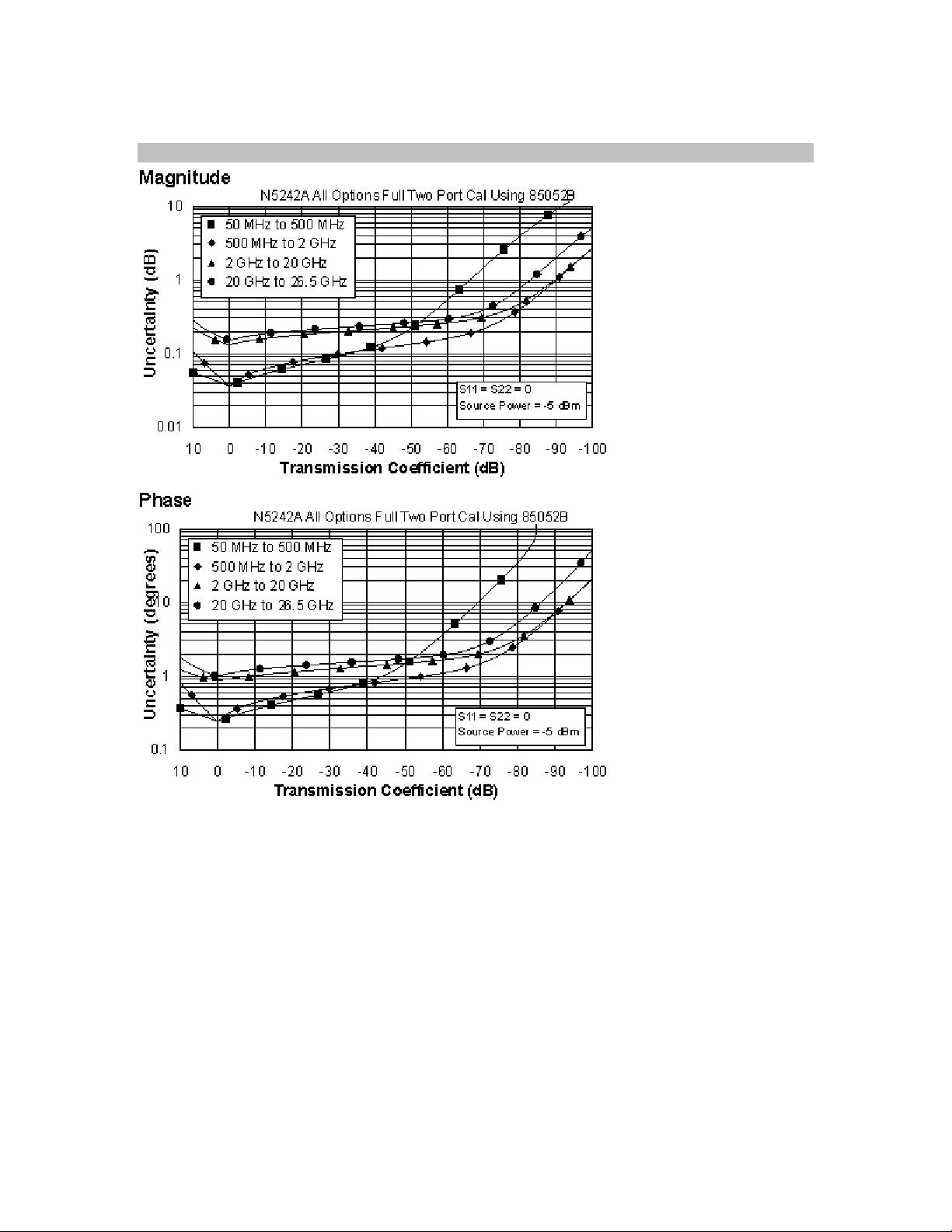
Transmission Uncertainty (Specifications)
14
Page 19

Reflection Uncertainty (Specifications)
15
Page 20

Table 4. N4433A 4-Port Electronic Calibration Module N5242A
All Options
Note: Uncertainty curves for the N4433A are created using a 2-port calibration. Multiport
uncertainties are not supported at this time.
Applies to the N5242A Option 200 or 219 or 224 or 400 or 419 or 423 analyzers, N4433A
(3.5mm) electronic calibration module, 85131F flexible test port cable set, and a full 2-port
calibration. Also applies to the following condition:
Environmental temperature 23° ±3 °C, with < 1 °C deviation from calibration temperature
Description Specification (dB)
50 MHz to
500 MHz
500 MHz to
2 GHz
2 to
20 GHz
Directivity 52 52 45
Source Match 42 42 31
Load Match 41 41 29
Reflection Tracking 1 ±0.060
+0.010/°C
Transmission Tracking 1 ±0.063
+0.010/°C
1
Temperature deviation is a characteristic value.
±0.060
+0.010/°C
±0.063
+0.010/°C
±0.180
+0.020/°C
±0.197
+0.020/°C
16
Page 21
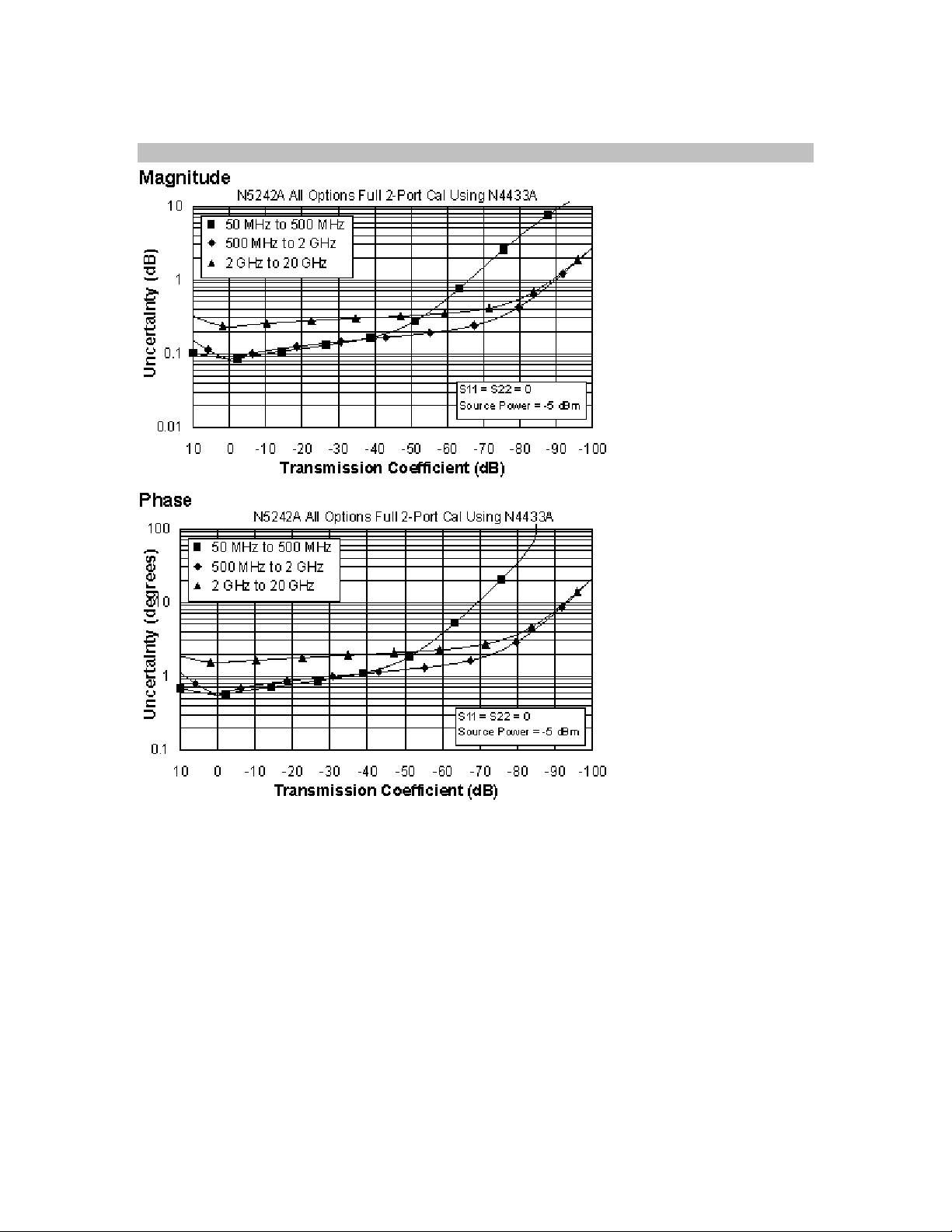
Transmission Uncertainty (Specifications)
17
Page 22

Reflection Uncertainty (Specifications)
18
Page 23

Table 5. N4691B 2- Port Electronic Calibration Module
N5242A All Options
Applies to the N5242A Option 200 or 219 or 224 or 400 or 419 or 423 analyzers, N4691B
(3.5mm) electronic calibration module, 85131F flexible test port cable set, and a full 2-port
calibration. Also applies to the following condition:
Environmental temperature 23° ±3 °C, with < 1 °C deviation from calibration temperature
Description Specification (dB)
50 MHz to
500 MHz
500 MHz to
2 GHz
2 to
20 GHz
20 to
26.5 GHz
Directivity 46 56 48 44
Source Match 41 47 44 40
Load Match 40 46 42 38
Reflection Tracking 1 ±0.050
+0.010/°C
Transmission Tracking 1 ±0.056
+0.010/°C
1
Temperature deviation is a characteristic value.
±0.020
+0.010/°C
±0.022
+0.010/°C
±0.040
+0.020/°C
±0.052
+0.020/°C
±0.050
+0.030/°C
±0.072
+0.030/°C
19
Page 24

Transmission Uncertainty (Specifications)
20
Page 25

Reflection Uncertainty (Specifications)
This N5242A document does not present specifications for the 85052C or 85052D Calibration Kit.
Please download our free Uncertainty Calculator from http://www.agilent.com/find/na_calculator
to generate the data and curves for the 85052C or the 85052D Calibration Kit.
21
Page 26

Uncorrected System Performance
Table 6. Error Terms
1
All Options - Ports 1, 2, 3, 4
Description Specification Typical
Directivity (dB)
10 MHz to 50 MHz 16 23
50 MHz to 500 MHz 24 28
500 MHz to 3.2 GHz 24 32
3.2 GHz to 10 GHz 23 25
10 GHz to 16 GHz 16 22
16 GHz to 20 GHz 16 22
20 GHz to 24 GHz 16 22
24 GHz to 26.5 GHz 16 22
Source Match (dB)
10 MHz to 50 MHz 11 14
50 MHz to 500 MHz 18 28
500 MHz to 3.2 GHz 18 22
3.2 GHz to 10 GHz 14 18
10 GHz to 16 GHz 12 16
16 GHz to 20 GHz 10 15
20 GHz to 24 GHz 10 14
24 GHz to 26.5 GHz 8 12
Load Match (dB)
10 MHz to 50 MHz 11 18
50 MHz to 500 MHz 17 25
500 MHz to 3.2 GHz 17 22
3.2 GHz to 10 GHz 13 17
10 GHz to 16 GHz 10 15
16 GHz to 20 GHz 9 14
20 GHz to 24 GHz 9 14
22
Page 27

Description Specification Typical
24 GHz to 26.5 GHz 8 13
Transmission Tracking3 (dB)
10 MHz to 50 MHz
50 MHz to 500 MHz
500 MHz to 3.2 GHz
3.2 GHz to 10 GHz
10 GHz to 16 GHz
16 GHz to 20 GHz
20 GHz to 24 GHz
24 GHz to 26.5 GHz
Reflection Tracking (dB)
10 MHz to 50 MHz
50 MHz to 500 MHz
500 MHz to 3.2 GHz
3.2 GHz to 10 GHz
10 GHz to 16 GHz
-- +/-1.5
-- +/-1.5
16 GHz to 20 GHz
20 GHz to 24 GHz
24 GHz to 26.5 GHz
23
Page 28

Crosstalk
10 MHz to 50 MHz -84
4
(dB)
-50 MHz to 100 MHz -90
100 MHz to 500 MHz -110
500 MHz to 3.2 GHz -120
3.2 GHz to 20 GHz -122
20 GHz to 24 GHz -117
24 GHz to 26.5 GHz
1
Specifications apply over environmental temperature of 25 °C ±5 °C, with less than 1°C variation
-114
from the calibration temperature.
3
Cable loss not included.
4
Measurement conditions: normalized to a thru, measured with two shorts, 10 Hz IF bandwidth,
averaging factor of 8, alternate mode, source power set to the lesser of the maximum power-out
or the maximum receiver power.
24
Page 29

Test Port Output
Table 7. Frequency Information
All Options
Description Specification (dB) Typical (dB)
Frequency Range 10 MHz to 26.5 GHz -Frequency Resolution 1 Hz -Frequency Accuracy +/- 1 ppm -Frequency Stability -- +/-0.05 ppm, -10° to 70° C
+/-0.1 ppm/yr maximum
Table 8a. Maximum Leveled Power, Option 200 or 400
Description Specification (dBm) Typical (dBm)
Port 1 or
1
3
Filtered
2
Mode
See Figure
2 (Opt
200) or
Figure 5
(Opt 400)
Port 1 or
1
3
Hi Pwr
2
Mode
See
Figure 3
(Opt 200)
or Figure
6 (Opt
400)
Port 2 or
1
4
Port 1 or
31
Filtered
Mode
See
Figure 2
(Opt 200)
or Figure
5 (Opt
400)
2
Port 1 or 3
Hi Pwr
2
Mode
See Figure
3 (Opt
200) or
Figure 6
(Opt 400)
1
Port 2 or
1
4
10 MHz to 50
8 13 13 10 19 17
MHz
50 MHz to 500
10 13 13 11 21 20
MHz
500 MHz to 3.2
10 10 13 12 13 18
GHz
3.2 GHz to 10
13 13 13 20 20 19
GHz
10 GHz to 16 GHz 13 13 13 17 17 16
16 GHz to 20 GHz 13 13 10 16 16 12
20 GHz to 24 GHz 12 12 7 15 15 11
24 GHz to 26.5
5 5 2 11 11 7
GHz
1
Either port can be used as the source port.
2
In Filtered Mode, the signal path goes through filters to minimize harmonics below 3.2 GHz. In Hi Pwr Mode, the signal
bypasses the filters to maximize output power.
25
Page 30

Figure 1. Block Diagram, N5242A Option 200
Figure 2. Path Configuration Diagram, N5242A Option 200, Port 1 Filtered Mode
Port 1 Reference
Mixer Switch
Front Panel
Jumper
R1
Port 1 or 3 Filtered Mode
Low Bnd
Hi Pwr
Low Bnd
Filtered
OUT1
External
Internal
A
1
OUT2
Src1
R2 B
2
26
Page 31

Figure 3. Path Configuration Diagram, N5242A Option 200, Port 1 Hi Pwr Mode
Port 1 Reference
Mixer Switch
Front Panel
Jumper
R1
Port 1 or 3 Hi Pwr Mode
Low Bnd
Hi Pwr
Low Bnd
Filtered
OUT1
External
Internal
A
1
Src1
OUT2
Figure 4. Block Diagram, N5242A Option 400
R2 B
2
27
Page 32

Figure 5. Path Configuration Diagram, N5242A Option 400, Port 1 or 3 Filtered Mode
R4 D
OUT2
Low Bnd
Filtered
Low Bnd
Hi Pwr
Port 1 or 3
Hi Pwr Mode
Low Bnd
Hi Pwr
Low Bnd
Filtered
OUT2
Src2
Src1
OUT1
OUT1
Port 1 Reference
Mixer Switch
Front Panel
Jumper
External
Internal
4
R3 C
3
R1
A
1
R2 B
2
28
Page 33

Figure 6. Path Configuration Diagram, N5242A Option 400, Port 1 or 3 Hi Pwr Mode
R4 D
OUT2
Low Bnd
Filtered
Low Bnd
Hi Pwr
Port 1 or 3
Filtered Mode
Low Bnd
Hi Pwr
Low Bnd
Filtered
OUT2
Src2
Src1
OUT1
OUT1
Port 1 Reference
Mixer Switch
Front Panel
Jumper
External
Internal
4
R3 C
3
R1
A
1
R2 B
2
29
Page 34

Table 8b. Maximum Leveled Power, Option 219 or 419
Description Specification (dBm) Typical (dBm)
Port 1 or
1
3
Filtered
2
Mode
10 MHz to 50
8 13 13 10 19 17
Port 1 or
1
3
Hi Pwr
2
Mode
Port 2 or
1
4
Port 1 or
31
Filtered
2
Mode
Port 1 or
1
3
Hi Pwr
Mode
2
Port 2 or
4
MHz
50 MHz to 500
10 13 13 11 20 19
MHz
500 MHz to 3.2
10 10 13 11 13 18
GHz
3.2 GHz to 10
13 13 13 18 18 17
GHz
10 GHz to 16 GHz 12 12 11 15 15 14
16 GHz to 20 GHz 10 10 8 13 13 10
20 GHz to 24 GHz 8 8 7 12 12 9
24 GHz to 26.5
3 3 -1 8 8 4
GHz
1
1
Either port can be used as the source port.
2
In Filtered Mode, the signal path goes through filters to minimize harmonics below 3.2 GHz. In
Hi Pwr Mode, the signal bypasses the filters to maximize output power.
Figure 7. Block Diagram, N5242A Option 219
Note: The path configuration drawing for Option 219 is identical to the path configuration
drawings for Option 200, which are shown in Figure 2 and Figure 3.
30
Page 35

Figure 8. Block Diagram, N5242A Option 419
Note: The path configuration drawing for Option 419 is identical to the path configuration
drawings for Option 400, which are shown in Figure 5 and Figure 6.
Table 8c. Maximum Leveled Power, Option 224
Description Specification (dBm) Typical (dBm)
Port 1
Filtered
Mode
Port 1
Hi Pwr
1
Mode
1
Port 2 Port 1
Filtered
Mode
1
Port 1
Hi Pwr
Mode
Port 2
1
10 MHz to 50 MHz 7 13 13 9 19 17
50 MHz to 500
8 13 13 11 20 20
MHz
500 MHz to 3.2
8 10 13 11 13 17
GHz
3.2 GHz to 10 GHz 13 13 13 19 19 17
10 GHz to 16 GHz 12 12 10 15 15 14
16 GHz to 20 GHz 10 10 7 13 13 10
20 GHz to 24 GHz 7 7 5 12 12 9
24 GHz to 26.5
0 0 -2 8 8 4
GHz
1
In Filtered Mode, the signal path goes through filters to minimize harmonics below 3.2 GHz. In
Hi Pwr Mode, the signal bypasses the filters to maximize output power.
31
Page 36

Table 8d. Maximum Leveled Power, Option 224
Description Specification (dBm) Typical (dBm)
Source 2,
Out 1
Filtered
1
Mode
Source 2,
Out 1
Hi Pwr
1
Mode
Source 2,
Out 2
Source 2,
Out 1
Filtered
Mode
1
Source 2,
Out 1
Hi Pwr
1
Mode
Source
2, Out
10 MHz to 50 MHz 9 18 13 12 21 18
50 MHz to 500 MHz 11 18 17 13 22 21
500 MHz to 3.2 GHz 10 14 14 13 17 19
3.2 GHz to 10 GHz 18 18 18 22 22 22
10 GHz to 16 GHz 16 16 16 21 21 20
16 GHz to 20 GHz 15 15 13 19 19 17
20 GHz to 24 GHz 13 13 12 18 18 17
24 GHz to 26.5 GHz 7 7 5 14 14 11
1
In Filtered Mode, the signal path goes through filters to minimize harmonics below 3.2 GHz. In
Hi Pwr Mode, the signal bypasses the filters to maximize output power.
Figure 9. Block Diagram: N5242A Option 224
2
32
Page 37

Figure 10. Path Configuration Diagram, N5242A Option 224
OUT2
Src2
Low Bnd
Filtered
Low Bnd
Hi Pwr
Combiner
Normal
Reversed
Low Bnd
Hi Pwr
Low Bnd
Filtered
OUT2
Src1
OUT1
OUT1
Rear Panel
Jumper
J8J9
Port 1 Bypass Switch
J10 J11
Rear Panel
Jumper
Port 2 Source
Src2 OUT1
Src1 OUT2
Combiner Path
Thru Path
Src 2 Main Bypass Switch
Port 2 Bypass Switch
J1 J2
Thru Path
Combiner Path
Port 1 Reference
Mixer Switch
Front Panel
Jumper
External
Internal
Rear Panel
Thru Path
OUT2 (Front Panel)
OUT1 (Front Panel)
R1
A
1
R2 B
2
Table 8e. Maximum Leveled Power, Option 423
Description Specification (dBm) Typical (dBm)
Port 1 or 3
Filtered
Mode
10 MHz to 50 MHz 7 13 13 9 19 17
50 MHz to 500
8 13 13 11 20 20
MHz
500 MHz to 3.2
8 10 13 11 13 17
GHz
3.2 GHz to 10
13 13 13 19 19 17
GHz
10 GHz to 16 GHz 12 12 10 15 15 14
16 GHz to 20 GHz 10 10 7 13 13 10
20 GHz to 24 GHz 7 7 5 12 12 9
24 GHz to 26.5
0 0 -2 8 8 4
GHz
1
Port 1 or 3
Hi Pwr
1
Mode
Port 2 or 4 Port 1 or 3
Filtered
1
Mode
Port 1 or 3
Hi Pwr
1
Mode
Port 2 or 4
1
In Filtered Mode, the signal path goes through filters to minimize harmonics below 3.2 GHz. In
Hi Pwr Mode, the signal bypasses the filters to maximize output power.
33
Page 38

Table 8f. Maximum Leveled Power, Option 224 or 423
Description Typical (dBm)
Source 1, Port 1
Combine Mode
1
10 MHz to 50
Filtered Mode
7 17 -7 3
MHz
50 MHz to 500
9 17 -5 4
MHz
500 MHz to 3.2
9 10 -5 -4
GHz
3.2 GHz to 10
15 15 2 2
GHz
10 GHz to 16
11 11 -2 -2
GHz
16 GHz to 20
8 8 -4 -4
GHz
20 GHz to 24
6 6 -6 -6
GHz
24 GHz to 26.5
2 2 -11 -11
GHz
Source 1, Port 1
Combine Mode
Hi Pwr Mode
Source 2, Port 1
Combine Mode
1
Filtered Mode
Source 2, Port 1
Combine Mode
Hi Pwr Mode
1
1
1
In Filtered Mode, the signal path goes through filters to minimize harmonics below 3.2 GHz. In
Hi Pwr Mode, the signal bypasses the filters to maximize output power.
Figure 11. Block Diagram: N5242A Option 423
34
Page 39

Figure 12. Path Configuration Diagram, N5242A Option 423
Port 4 Bypass Switch
J3 J4
OUT2
Rear Panel
Thru Path
R4 D
4
Src2
Low Bnd
Filtered
Low Bnd
Hi Pwr
OUT1
Rear Panel
Jumper
J8J9
Combiner
Normal
Reversed
Low Bnd
Hi Pwr
Low Bnd
Filtered
OUT2
OUT1
Src1
Port 1 Bypass Switch
J10 J11
Rear Panel
Jumper
Table 9a. Power Level Accuracy
All Options
Rear Panel
Load
Combiner Path
Thru Path
Port 3 Bypass Switch
J7
Port 2 Bypass Switch
J1 J2
Thru Path
Combiner Path
Port 1 Reference
Mixer Switch
Front Panel
Jumper
External
Internal
Rear Panel
Thru Path
R3 C
3
R1
A
1
R2 B
2
Description Specification (dB) Typical (dB)
Ports 1, 2, 3, 41 Source 2, Out 1
Source 2, Out 2
Ports 1, 2, 3, 41 Source 2, Out 1
Source 2, Out 2
10 MHz to 50 MHz +/-1.0 +/-2.0 +/-0.40 +/-0.55
50 MHz to 500 MHz +/-1.0 +/-2.0 +/-0.20 +/-0.25
500 MHz to 3.2 GHz +/-1.0 +/-2.0 +/-0.25 +/-0.25
3.2 GHz to 10 GHz +/-1.0 +/-2.0 +/-0.40 +/-0.25
10 GHz to 13 GHz +/-1.2 +/-2.0 +/-0.60 +/-0.25
13 GHz to 18 GHz +/-2.0 +/-2.5 +/-0.60 +/-1.00
18 GHz to 26.5 GHz +/-2.5 +/-2.5 +/-0.80 +/-0.90
1
Any port can be used as the source port. Source in filtered mode where applicable.
35
Page 40

Table 9b. Power Level Linearity
All Options
Description Specification (dB)
Port 1 or 31
-25dBm ≤ P<-20dBm
Port 1 or 31
-20dBm ≤ P<-15dBm
Port 1 or 31
P ≥-15dBm
10 MHz to 50 MHz +/-2.0 +/-1.5 +/-1.0
50 MHz to 500 MHz +/-1.5 +/-1.0 +/-1.0
500 MHz to 3.2 GHz +/-1.0 +/-1.0 +/- 1.0
3.2 GHz to 10 GHz +/-1.0 +/-1.0 +/-1.0
10 GHz to 16 GHz +/-1.0 +/-1.0 +/-1.0
16 GHz to 20 GHz +/-1.0 +/-1.0 +/-1.0
20 GHz to 24 GHz +/-1.0 +/-1.0 +/-1.0
24 GHz to 26.5 GHz +/-1.0 +/-1.0 +/-1.0
1
Either port can be used as the source port. Source in filtered mode.
Table 9c. (Continued) Power Level Linearity
All Options
Description Specification (dB)
Port 2 or 41
-25dBm ≤P<-20dBm
Port 2 or 41
-20dBm ≤P<-15dBm
Port 2 or 41
P ≥-15dBm
10 MHz to 50 MHz +/-5.0 +/-2.0 +/-1.5
50 MHz to 500 MHz +/-4.0 +/-2.0 +/-1.5
500 MHz to 3.2 GHz +/-2.5 +/-1.0 +/-1.0
3.2 GHz to 10 GHz +/-2.0 +/-1.0 +/-1.0
10 GHz to 16 GHz +/-1.5 +/-1.5 +/-1.5
16 GHz to 20 GHz +/-1.0 +/-1.0 +/-1.0
20 GHz to 24 GHz +/-1.0 +/-1.0 +/-1.0
24 GHz to 26.5 GHz +/-1.0 +/-1.0 +/-1.0
1
Either port can be used as the source port.
36
Page 41

Table 9d. Power Level Linearity
Option 224
Description Specification (dB)
Source 2, Out 11
P ≥-15dBm
Source 2, Out 2
-15dBm ≤P<-10dBm
Source 2, Out 2
P ≥-10dBm
10 MHz to 50 MHz +/-1.0 +/-1.5 +/-1.0
50 MHz to 500 MHz +/-1.0 +/-1.5 +/-1.0
500 MHz to 3.2 GHz +/-1.0 +/-1.0 +/-1.0
3.2 GHz to 10 GHz +/-1.0 +/-1.0 +/-1.0
10 GHz to 16 GHz +/-1.0 +/-1.0 +/-1.0
16 GHz to 20 GHz +/-1.0 +/-1.0 +/-1.0
20 GHz to 24 GHz +/-1.0 +/-1.0 +/-1.0
24 GHz to 26.5 GHz +/-1.0 +/-1.0 +/-1.0
1Source in filtered mode.
Table 10a. Power Sweep Range
Option 200 or 400
Description Specification (dB) Typical (dB)
Port 1 or 31 Port 2 or 41 Port 1 or 31 Port 2 or 41
10 MHz to 50 MHz 38 38 46 44
50 MHz to 500 MHz 38 38 48 47
500 MHz to 3.2 GHz 35 38 40 45
3.2 GHz to 10 GHz 38 38 47 46
10 GHz to 16 GHz 38 38 44 43
16 GHz to 20 GHz 38 35 43 39
20 GHz to 24 GHz 37 32 42 38
24 GHz to 26.5 GHz 30 27 38 34
1
Either port can be used as the source port. Source in filtered mode where applicable.
37
Page 42

Table 10b. Power Sweep Range
Option 219 or 419
Description Specification (dB) Typical (dB)
Port 1 or 31 Port 2 or 41 Port 1 or 31 Port 2 or 41
10 MHz to 50 MHz 38 38 46 44
50 MHz to 500 MHz 38 38 47 46
500 MHz to 3.2 GHz 35 38 40 45
3.2 GHz to 10 GHz 38 38 45 44
10 GHz to 16 GHz 37 36 42 41
16 GHz to 20 GHz 35 33 40 37
20 GHz to 24 GHz 33 32 39 36
24 GHz to 26.5 GHz 28 24 35 31
1
Either port can be used as the source port. Source in filtered mode where applicable.
Table 10c. Power Sweep Range
Option 224 or 423
Description Specification (dB) Typical (dB)
Port 1 or 31 Port 2 or 41 Port 1 or 31 Port 2 or 41
10 MHz to 50 MHz 38 38 46 44
50 MHz to 500 MHz 38 38 47 47
500 MHz to 3.2 GHz 35 38 40 44
3.2 GHz to 10 GHz 38 38 46 44
10 GHz to 16 GHz 37 35 42 41
16 GHz to 20 GHz 35 32 40 37
20 GHz to 24 GHz 32 30 39 36
24 GHz to 26.5 GHz 25 23 35 31
1
Either port can be used as the source port. Source in filtered mode where applicable.
38
Page 43

Table 10d. Power Sweep Range
Option 224
Description Specification (dB) Typical (dB)
Source 21
Out 1
Source 2
Out 2
Source 21
Out 1
Source 2
Out 2
10 MHz to 50 MHz 33 28 38 35
50 MHz to 500 MHz 33 32 39 38
500 MHz to 3.2 GHz 29 29 34 36
3.2 GHz to 10 GHz 33 33 39 39
10 GHz to 16 GHz 31 31 38 37
16 GHz to 20 GHz 30 28 36 34
20 GHz to 24 GHz 28 27 35 34
24 GHz to 26.5 GHz 22 20 31 28
1
Source in filtered mode where applicable.
Table 11. Nominal Power (Preset Power)
Description Specification (dBm) Typical (dBm)
Option
200 or
400
Option 219
or 224 or
419 or 423
Option 224 Option 224
or 423
Ports 1, 2, 3, 41 Source 2,
Out 1
Source 2,
Out 2
Source 1,
Port 1
Combine
Mode
10 MHz to 26.5
0 -5 5 5 -10 -15
GHz
1
Any port can be used as the source port. Any other port can be used as the receiver port.
39
Source 2,
Port 1
Combine
Mode
Page 44

Table 12. Power Resolution and Maximum/Minimum Settable Power
Description Specification
Typical at Test Port
at Test Port
All Options All Options Option 200 or
Option 219 or
400
Ports 1, 2, 3, 41
Power Resolution 0.01 dB -- -- -Maximum Settable
-- 30 dBm -- --
Power
Minimum Settable
-- -- -30 dBm -95 dBm
Power
1
Any port can be used as the source port.
419
40
Page 45

Table 13. Harmonics at Max Specified Power
All Options
(See Tables 8a - 8f Maximum Leveled Power)
Description Typical (dBc)
Port 1 or 31,2
Source 2 Out 1
2nd Harmonics3
10 MHz to 50 MHz -51 -13
50 MHz to 2 GHz -51 -13
2 GHz to 3.2 GHz -60 -21
3.2 GHz to 10 GHz -60 -21
10 GHz to 16 GHz -60 -21
16 GHz to 20 GHz -60 -21
20 GHz to 24 GHz -60 -21
24 GHz to 26.5 GHz -60 -21
3rd Harmonics3
10 MHz to 50 MHz -51 -13
50 MHz to 2 GHz -51 -13
Port 2 or 41
Source 2 Out 2
2 GHz to 3.2 GHz -60 -21
3.2 GHz to 10 GHz -60 -21
10 GHz to 16 GHz -60 -21
16 GHz to 20 GHz -60 -21
20 GHz to 24 GHz -60 -21
24 GHz to 26.5 GHz -60 -21
41
Page 46

1/2 and 1/4 Sub-Harmonics
3
10 MHz to 50 MHz -73 -73
50 MHz to 2 GHz -73 -73
2 GHz to 3.2 GHz -73 -73
3.2 GHz to 10 GHz -66 -63
10 GHz to 16 GHz -66 -63
16 GHz to 20 GHz -66 -63
20 GHz to 24 GHz -61 -52
24 GHz to 26.5 GHz -61 -52
1
Any port can be used as the source port.
2
< 3.2 GHz Filtered Mode
3
Listed frequency is fundamental frequency; test at max specified power
Table 14. Non-Harmonic Spurs at nominal power
Description Typical (dBc) at Test Port
Ports 1, 2, 3, 4
Source 2 Out 1,
Source 2 Out 2
Offset frequency = 30 kHz to 5 MHz
10 MHz to 500 MHz -50
500 MHz to 1 GHz -60
1 GHz to 2 GHz -60
2 GHz to 4 GHz -57
4 GHz to 8 GHz -51
8 GHz to 16 GHz -45
16 GHz to 24 GHz -39
24 GHz to 26.5 GHz -33
42
Page 47

Table 15. Phase Noise
All Options
Description Typical (dBc/Hz)
Ports 1, 2, 3, 4, Source 2 Out 1, Source 2 Out 2
1 kHz Offset 10 kHz Offset 100 kHz Offset 1 MHz Offset
10 MHz to 500 MHz -85 -85 -85 -120
500 MHz to 1 GHz - 105 -115 -110 -127
1 GHz to 2 GHz -100 -110 -105 -121
2 GHz to 4 GHz -95 -105 -100 -115
4 GHz to 8 GHz -89 -100 -94 -110
8 GHz to 16 GHz -83 -94 -88 -105
16 GHz to 26.5 GHz -78 -89 -82 -100
43
Page 48

Test Port Input
Table 16. Test Port Input
All Options
Description Specification Typical
Ports 1, 2, 3, 4
Test Port Noise Floor1 (dBm)
10 Hz IFBW
10 MHz to 50 MHz2 -80 -87
50 MHz to 100 MHz2 -90 -95
100 MHz to 500 MHz2 -104 -110
500 MHz to 2 GHz -114 -117
2 GHz to 20 GHz -114 -117
20 GHz to 24 GHz -110 -115
24 GHz to 26.5 GHz -107 -113
Direct Receiver Access Input Noise Floor1 (dBm)
10 Hz IFBW
10 MHz to 50 MHz2 -- -130
50 MHz to 100 MHz2 -- -128
100 MHz to 500 MHz2 -- -132
500 MHz to 2 GHz -- -133
2 GHz to 20 GHz -- -129
20 GHz to 24 GHz -- -122
24 GHz to 26.5 GHz -- -119
44
Page 49

Test Port Compression at 0.1 dB (dBm)
10 MHz to 50 MHz -- -50 MHz to 500 MHz -- -500 MHz to 3.2 GHz -- 13
3.2 GHz to 10 GHz -- 13
10 GHz to 16 GHz -- 13
16 GHz to 20 GHz -- 12
20 GHz to 24 GHz -- 10.5
24 GHz to 26.5 GHz -- 10
Receiver Compression @ 8 dBm Test Port Power (dB)
10 MHz to 50 MHz3 -- -50 MHz to 500 MHz3 -- -500 MHz to 3.2 GHz <0.17 --
3.2 GHz to 10 GHz <0.17 -10 GHz to 16 GHz <0.17 -16 GHz to 20 GHz <0.23 -20 GHz to 24 GHz <0.23 -24 GHz to 26.5 GHz <0.29 --
45
Page 50

Table 16.(Continued) Test Port Input
All Options - Ports 1, 2, 3, 4
Description Specification Typical
Trace Noise Magnitude (dB rms)
Ratioed measurement, nominal power at test port.
1 kHz IFBW
10 MHz to 100 MHz 0.007 0.0039
100 MHz to 13.5 GHz 0.002 0.0005
13.5 GHz to 16 GHz 0.002 0.0005
16 GHz to 22.5 GHz 0.002 0.0006
22.5 GHz to 24 GHz 0.003 0.0014
24 GHz to 26.5 GHz 0.005 0.0020
100 kHz IFBW
10 MHz to 100 MHz -- 0.040
100 MHz to 13.5 GHz -- 0.005
13.5 GHz to 16 GHz -- 0.005
16 GHz to 22.5 GHz -- 0.005
22.5 GHz to 24 GHz -- 0.008
24 GHz to 26.5 GHz -- 0.008
600 kHz IFBW
10 MHz to 100 MHz -- 0.140
100 MHz to 13.5 GHz -- 0.011
13.5 GHz to 16 GHz -- 0.011
16 GHz to 22.5 GHz -- 0.012
22.5 GHz to 24 GHz -- 0.020
24 GHz to 26.5 GHz -- 0.020
46
Page 51

Trace Noise Phase (deg rms)
Ratioed measurement, nominal power at test port.
1 kHz IFBW
10 MHz to 100 MHz 0.051 0.0261
100 MHz to 13.5 GHz 0.015 0.0041
13.5 GHz to 16 GHz 0.042 0.0124
16 GHz to 22.5 GHz 0.042 0.0135
22.5 GHz to 26.5 GHz 0.054 0.0225
100 kHz IFBW
10 MHz to 100 MHz -- 0.266
100 MHz to 13.5 GHz -- 0.030
13.5 GHz to 16 GHz -- 0.030
16 GHz to 22.5 GHz -- 0.033
22.5 GHz to 26.5 GHz -- 0.057
600 kHz IFBW
10 MHz to 100 MHz -- 1.053
100 MHz to 13.5 GHz -- 0.075
13.5 GHz to 16 GHz -- 0.075
16 GHz to 22.5 GHz -- 0.082
22.5 GHz to 26.5 GHz -- 0.139
Reference Level Magnitude
Range +/-500 dB -Resolution 0.001 dB --
Reference Level Phase
Range +/-500° -Resolution 0.01° --
47
Page 52

Stability Magnitude (dB/°C)
Stability is defined as a ratio measurement made at the test
port.
10 MHz to 50 MHz -- 0.01
50 MHz to 500 MHz -- 0.01
500 MHz to 3.2 GHz -- 0.01
3.2 GHz to 10 GHz -- 0.02
10 GHz to 16 GHz -- 0.02
16 GHz to 20 GHz -- 0.03
20 GHz to 24 GHz -- 0.03
24 GHz to 26.5 GHz -- 0.04
Table 16. (Continued)Test Port Input
All Options - Ports 1, 2, 3, 4
Description Specification Typical
Stability Phase (dB/°C)
Stability is defined as a ratio measurement made at the test port.
10 MHz to 50 MHz -- 0.29
50 MHz to 500 MHz -- 0.06
500 MHz to 3.2 GHz -- 0.07
3.2 GHz to 10 GHz -- 0.13
10 GHz to 16 GHz -- 0.13
16 GHz to 20 GHz -- 0.40
20 GHz to 24 GHz -- 0.54
24 GHz to 26.5 GHz -- 0.56
48
Page 53

Table 16. (Continued)Test Port Input
Description Typical
Damage Input Level
Test Port 1 or 2 or 3 or 4 > +30 dBm RF, 40 VDC
(Option 224 only) Source 2 Out 1
> +30 dBm RF, 0 VDC
or Source 2 Out 2
1
Total average (rms) noise power calculated as the mean value of a linear magnitude trace
expressed in dBm.
2
May typically be degraded at particular frequencies below 500 MHz due to spurious receiver
residuals.
3
Test port receiver compression at specified input levels below 500 MHz is negligible due to
coupler roll off in this frequency range.
49
Page 54

Dynamic Accuracy
Table 17 Dynamic Accuracy (Specification)
Accuracy of the test port input power reading relative to the reference input power level.
Dynamic Accuracy, 0.010 GHz
50
Page 55

Dynamic Accuracy, 0.050 GHz
51
Page 56

Dynamic Accuracy, 0.500 GHz
52
Page 57

Dynamic Accuracy, 1- 10 GHz
53
Page 58

Dynamic Accuracy, 10 - 16 GHz
54
Page 59

Dynamic Accuracy, 16 - 20 GHz
55
Page 60

Dynamic Accuracy, 20 - 26.5 GHz
2
Dynamic accuracy is verified with the following measurements:
Compression over frequency
IF linearity at a single frequency of 1.195 GHz using a reference level of -20 dBm for an input
power range of 0 to -120 dBm.
56
Page 61

Table 18. Test Port Input (Group Delay)a
Description Typical Performance
Aperture (selectable) (frequency span)/(number of points -1)
Maximum Aperture 20% of frequency span
Range 0.5 x (1/minimum aperture)
Maximum Delay Limited to measuring no more than 180° of phase change
within the minimum aperture.)
Accuracy See graph below. Char.
The following graph shows characteristic group delay accuracy with full 2-port calibration and a
10 Hz IF bandwidth. Insertion loss is assumed to be < 2 dB and electrical length to be ten meters.
For any S
Group Delay measurement, Sii = 0, Sij = 1, Sji = 0, Skl = 0 for all kl ≠ ij
ij
In general, the following formula can be used to determine the accuracy, in seconds, of specific
group delay measurement:
±Phase Accuracy (deg)/[360 × Aperture (Hz)]
Depending on the aperture and device length, the phase accuracy used is either incremental
phase accuracy or worst-case phase acc uracy.
a
Group delay is computed by measuring the phase change within a specified frequency step
(determined by the frequency span and the number of points per sweep).
57
Page 62

General Information
• Miscellaneous Information
• Front Panel
• Rear Panel
• Environment and Dimensions
Table 19. Miscellaneous Information
Description Supplemental Information
System IF Bandwidth Range 1 Hz to 5 MHz, nominal
CPU Intel® 1.6 GHz Pentium® M with 1 GByte RAM
Table 20. Front Panel Information
All Options
Description Typical Performance
RF Connectors
Type Option 200 or 219 or 224 or 400 or 419 or 423: 3.5 mm (male), 50
ohm, (nominal)
Center Pin
Recession
USB 2.0 Ports
Master (4 ports)
Standard Compatible with USB 2.0
Connector USB Type-A female
Display
Size 26.3 cm (10.4 in) diagonal color active matrix LCD; 1024 (horizontal)
Refresh Rate Vertical 60 Hz; Horizontal 46.08 kHz
Pixels A display is considered faulty if:
0.002 in. (characteristic)
X 768 (vertical) resolution
More than 0.002% of the total pixels have a constant blue, green, red,
or black appearance that will not change.
Three or more consecutive pixels have a constant blue, green, red, or
black appearance that will not change.
58
Page 63

Display Range
Magnitude +/-2500 dB (at 500 dB/div), max
Phase +/-2500° (at 500 dB/div), max
Polar 10 pUnits, min
10,000 Units, max
Display Resolution
Magnitude 0.001 dB/div, min
Phase 0.01°/div, min
Marker Resolution
Magnitude 0.001 dB, min
Phase 0.01°, min
Polar 10 pUnit, min
59
Page 64

Table 21 Rear Panel Information
All Options
Description Typical Performance
10 MHz Reference In
Connector BNC, female
Input Frequency 10 MHz ± 10 ppm, typical
Input Level -15 dBm to +20 dBm, typical
Input Impedance
10 MHz Reference Out
Connector BNC, female
Output Frequency 10 MHz ± 1 ppm, typical
Signal Type Sine Wave, typical
Output Level
Output Impedance
Harmonics <-40 dBc, typical
External IF Inputs
Function Allows use of external IF signals from
Connectors SMA (female); A, B, C, D, R (4-port); A,
Input Frequency VNA IF (2.54 MHz, 7.61 MHz, or 10.73
200 Ω, nom.
+10 dBm ± 4 dB into 50 Ω
50 Ω, nominal
remote mixers, bypassing the PNA's first
converters
B, R1, R2 (2-port)
MHz)
Input Impedance
RF Damage Level
DC Damage Level 5.5 VDC
0.1 dB Compression
Point
50 Ω
60
Page 65

Pulse Inputs (IF Gates)
Function Internal receiver gates used for point-in-
pulse and pulse-profile measurements
Connectors 15-pin mini D-sub
Input Impedance 1 K Ohm
Minimum Pulse
Width, Source
Modulators
Minimum Pulse Width,
Receiver Gates
DC Damage Level 5.5 VDC
Drive Voltage 0 V (off), +3.3 V (on), nominal
RF Pulse Modulator Input (Source Modulator)
On/Off Ratio
10 MHz to 3.2 GHz -64
3.2 GHz to 26.5 GHz -80
Pulse Period
Minimum 33 ns
Maximum 70 s
External Test Set Driver
33 ns
20 ns
Function Used for driving remote mixers
Connections SMA (female)
RF, LO Output
Frequency Range
1.7 to 26.5 GHz
61
Page 66

Table 21. (Continued) Rear Panel Information
Description Typical (dBm)
Upper Limit
(dBm)
Test Set Drivers (Continued)
Rear Panel LO Power
1.7 GHz to 18 GHz 0 -10
18 GHz to 22.5 GHz 2 -8
22.5 GHz to 26.5 GHz 6 -5
Rear Panel RF Power
3.2 GHz to 20 GHz -3 -8
20 GHz to 26.5 GHz -8 -14
Lower Limit
(dBm)
62
Page 67

Table 21. (Continued) Rear Panel Information
Description Typical Performance
VGA Video Output
Connector 15-pin mini D-Sub; Drives VGA compatible monitors
Devices Supported:
Resolutions:
Flat Panel (TFT) 1024 X 768, 800 X 600, 640 X 480
Flat Panel (DSTN) 800 X 600, 640 X 480
CRT Monitor 1280 X 1024, 1024 X 768, 800 X 600, 640 X 480
Simultaneous operation of the internal and external displays is
allowed, but with 640 X 480 resolution only. If you change resolution,
you can only view the external display (internal display will "white
out").
Bias Tee Inputs
Connectors BNC(f) for ports 1, 2, 3 and 4
Fuse 500 mA
Maximum Bias Current +/-200 mA
Maximum Bias Voltage +/-40 VDC
Trigger Inputs/Outputs BNC(f), TTL/CMOS compatible
Test Set IO 25-pin D-Sub connector, available for external test set control.
Power IO 9-pin D-Sub, female; analog and digital IO
Handler IO 36-pin parallel I/O port; all input/output signals are default set to
negative logic; can be reset to positive logic via GPIB command.
63
Page 68

GPIB (two ports dedicated controller and
dedicated talker/listener)
Parallel Port (LPT1) 25-pin D-Sub miniature connector, female; provides connection to
Serial Port (COM 1) 9-pin D-Sub, male; compatible with RS-232
USB Port Four ports on front panel (all Host) and five ports (four Host and one
LAN 10/100BaseT Ethernet, 8-pin configuration; auto selects between the
Line Power
Frequency, Voltage 50/60 Hz for 100 240 VAC
Power supply is auto switching
Max 450 watts
Note: Option H11 is not available with the N5242A network analyzer.
24-pin D-sub (Type D-24), female; compatible with IEEE-488.
printers or any other parallel port peripherals
Device) on rear panel. Type A configuration (eight Host) and Type B
configuration (one Device), USB 2.0 compatible.
two data rates
64
Page 69

Table 22. Analyzer Dimensions and Weight
Cabinet
Dimensions
Excluding front and
rear panel hardware
and feet
Excluding front and
rear panel hardware
and feet. Including
rack-mount flanges.
Excluding front and
rear panel hardware
and feet. Including
rack-mount flanges
and handles.
As shipped including front panel
connectors, rear
panel bumpers, and
feet.
As shipped including
rack-mount flanges
Height Width Depth
266 mm
10.5 in
266 mm
10.5 in
EIA RU
266 mm
10.5 in
EIA RU
277 mm
10.9 in
277 mm
10.9 in
1
= 6
1
= 6
436 mm
17.4 in
482 mm
19.3 in
482 mm
19.3 in
436 mm
17.4 in
482 mm
19.3 in
514 mm
20.6 in
561 mm
22.4 in
581 mm
23.2 in
561 mm
22.4 in
561 mm
22.4 in
As shipped including
handles
As shipped including
rack-mount flanges
277 mm
10.9 in
277 mm
10.9 in
458 mm
18.3 in
482 mm
19.3 in
581 mm
23.2 in
581 mm
23.2 in
and handles
Weight
Option 200 or 219 or 224 Option 400 or 419
--
or 423
Net 27 kg (60 lb), nominal 37 kg (82 lb),
--
nominal
Shipping 43 kg (95 lb), nominal 53 kg (117 lb),
--
nominal
1
Network analyzer feet removed.
Note: For Regulatory and Environmental information, refer to the PNA Series Installation and
Quick Start Guide, located online at http://cp.literature.agilent.com/litweb/pdf/E8356-90001.pdf.
65
Page 70

Measurement Throughput Summary
• Typical Cycle Time for Measurement Completion
• Cycle Time vs. IF Bandwidth
• Cycle Time vs. Number of Points
• Data Transfer Time
Table 23. Typical Cycle Timea (ms) for Measurement Completion
All Options
Description Typical Performance
Number of Points
201 401 1601 16001
Start 9 GHz, Stop 10 GHz, 600 kHz IF bandwidth
Uncorrected 6 6.3 9.6 56
2-Port cal 20 21 28 134
Start 9 GHz, Stop 10 GHz, 10 kHz IF bandwidth
Uncorrected 36 53 200 1945
2-Port cal 80 115 405 3900
Start 9 GHz, Stop 10 GHz, 1 kHz IF bandwidth
Uncorrected 227 444 1740 17000
2-Port cal 460 900 3484 34000
Start 10 GHz, Stop 20 GHz, 600 kHz IF bandwidth
Uncorrected 26 33 54 85
2-Port cal 62 77 121 190
Start 10 GHz, Stop 20 GHz, 10 kHz IF bandwidth
Uncorrected 70 118 273 1958
2-Port cal 149 245 553 3922
Start 10 GHz, Stop 20 GHz, 1 kHz IF bandwidth
Uncorrected 236 459 1780 17300
2-Port Cal
400 926 3565 34600
66
Page 71

Start 10 MHz, Stop 26.5 GHz, 600 kHz IF bandwidth
Uncorrected 59 69 118 350
2-Port cal 125 147 244 707
Start 10 MHz, Stop 26.5 GHz, 10 kHz IF bandwidth
Uncorrected 94 156 480 2333
2-Port cal 196 320 968 4674
Start 10 MHz, Stop 26.5 GHz, 1 kHz IF bandwidth
Uncorrected 277 504 1873 17950
2-Port cal 561 1015 3756 35900
a
Includes sweep time, retrace time and band-crossing time. Analyzer display turned off with
DISPLAY:ENABLE OFF. Add 21 ms for display on. Data for one trace (S
) measurement.
11
Note: Option H08 and Option H11 are not available with the N5242A network analyzer.
67
Page 72

Table 24. Cycle Time vs. IF Bandwidth
Applies to the Preset condition (201 points, correction off) except for the following changes:
• CF = 10 GHz
• Span = 100 MHz
• Display off (add 21 ms for display on)
Description Typical Performance
IF Bandwidth (Hz) Cycle Time (ms)1 Trace Noise
600,000 5.00 0.009
100,000 6.84 0.003
30,000 11.6 0.002
10,000 29.0 0.001
3,000 71.8 0.0007
1,000 222 0.0004
300 640 0.0003
100 1826 0.0002
30 5982 <0.0002
10 17830 <0.0002
3 60000 <0.0002
a Cycle time includes sweep and retrace time.
68
Page 73

Table 25. Cycle Time vs. Number of Points
Applies to the Preset condition (correction off) except for the following changes:
• CF = 10 GHz
• Span = 100 MHz
• Display off (add 21 ms for display on)
Description Typical Performance
IF Bandwidth
(Hz)
1,000
10,000
Number of Points Cycle Time
(ms)
1
3 7.7
11 16.6
51 60
101 115
201 222
401 436
801 860
1,601 1,700
6,401 6,700
16,001 16,000
3 5.44
11 7.90
51 10.7
101 16.8
201 29.0
401 53.0
801 102
1,601 199
6,401 780
16,001 1950
69
Page 74

Description Typical Performance
IF Bandwidth
(Hz)
30,000
600,000
Number of Points Cycle Time
(ms)
1
3 5.7
11 5.9
51 6.5
101 8.2
201 11.8
401 18.8
801 32.8
1,601 60.5
6,401 228
16,001 566
3 5.4
11 5.4
51 5.5
101 5.6
201 5.9
401 6.3
801 7.2
1,601 9.6
6,401 25
16,001 56
a Cycle time includes sweep and retrace time.
70
Page 75

Table 26. Data Transfer Time (ms)
Description Typical Performance
Number of Points
201 401 1601 16,001
SCPI over GPIB
(Program executed on external PC2)
32-bit floating point 5.6 10.5 39.9 400
64-bit floating point 10.5 20.3 79.2 788
ASCII 46 92.5 370 3702
SCPI over SICL/LAN or TCP/IP Socket
(Program executed in the analyzer)
32-bit floating point 0.18 0.21 0.5 3.6
64-bit floating point 0.22 0.28 0.62 5.3
ASCII 6.3 12.3 47.3 470
COM3
(Program executed in the analyzer)
32-bit floating point <0.15 0.15 0.2 0.7
Variant type 0.75 1.2 4.5 50
DCOM over LAN3
(Program executed on external PC)
32-bit floating point <1.0 1.2 2.1 13
Variant type 2.7 4.5 15 150
1
Measured with the analyzer display off. Values will increase slightly if the analyzer display is on.
2
Measured when using the SCPI command DISPlay: VISible OFF.
3
Values are for real and imaginary pairs, with the analyzer display off.
Note: Specifications for Recall & Sweep Speed are not provided for the N5242A analyzers.
71
Page 76

Specifications: Front-Panel Jumpers
Model N5242A (PNA-X)
Note: All PNA-X options have the following front-panel jumpers for each port.
• Measurement Receiver Inputs
• Reference Receiver Inputs
• Reference Outputs (Source Out)
• Source Outputs
• Coupler Inputs
72
Page 77

Table 27 Measurement Receiver Inputs
(Rcvr A IN, Rcvr B IN, Rcvr C IN, Rcvr D IN) @ 0.1dB Typical Compression
Description Typical
All Options
Maximum Input Level
10 MHz to 50 MHz1 -50 MHz to 500 MHz1 -500 MHz to 3.2 GHz -2 dBm
3.2 GHz to 10 GHz -2 dBm
10 GHZ to 16 GHz -2 dBm
16 GHZ to 20 GHz -2.5 dBm
20 GHZ to 24 GHz -4 dBm
24 GHZ to 26.5 GHz -4 dBm
Damage Level
N5242A +15 dBm
Maximum DC Level
N5242A 0 V
1Test port receiver compression at specified input levels below 500 MHz is negligible due to
coupler roll off in this frequency range.
73
Page 78

Table 28. Reference Receiver Input
(RCVR R1 IN) @ Max Specified Output Power
Description Typical
Maximum Input Level
10 MHz to 50 MHz -8 dBm -3 dBm -9 dBm -8 dBm -3 dBm -6 dBm
50 MHz to 500 MHz -6 dBm -3 dBm -7 dBm -6 dBm -3 dBm -5 dBm
500 MHz to 3.2
GHz
3.2 GHz to 10 GHz -3 dBm -3 dBm -2 dBm -2 dBm -2 dBm -2 dBm
10 GHZ to 16 GHz -4 dBm -4 dBm -3 dBm -3 dBm -3 dBm -3 dBm
16 GHZ to 20 GHz -5 dBm -5 dBm -6 dBm -6 dBm -6 dBm -6 dBm
20 GHZ to 24 GHz -7 dBm -7 dBm -9 dBm -8 dBm -8 dBm -9 dBm
24 GHZ to 26.5
GHz
Option
200 or
400
Filtered
Mode
-6 dBm -6 dBm -7 dBm -5 dBm -5 dBm -5 dBm
-16 dBm -16 dBm -18 dBm -15 dBm -15 dBm -18 dBm
Option
200 or
400
Hi Pwr
Mode
Option
224 or
423
Filtered
Mode
Option
219 or
419
Filtered
Mode
Option
219 or
419
Hi Pwr
Mode
Option
224 or
423
Hi Pwr
Mode
Damage Level
+15 dBm
Maximum DC Level
+/-7 V
74
Page 79

Table 29. Reference Receiver Input
(RCVR R2 IN, RCVR R3 IN, RCVR R4 IN) @ Max Specified Output Power
Description Typical
Maximum Input Level
10 MHz to 50 MHz -6 dBm -1 dBm -1 dBm -6 dBm -1 dBm -1 dBm
50 MHz to 500 MHz -4 dBm -1 dBm -1 dBm -4 dBm -1 dBm -1 dBm
500 MHz to 3.2
GHz
3.2 GHz to 10 GHz 0 dBm 0 dBm 0 dBm 1 dBm 1 dBm 0 dBm
10 GHZ to 16 GHz 1 dBm 1 dBm 0 dBm 1 dBm 1 dBm 1 dBm
16 GHZ to 20 GHz 1 dBm 1 dBm -3 dBm 0 dBm 0 dBm -3 dBm
20 GHZ to 24 GHz 0 dBm 0 dBm -6 dBm -1 dBm -1 dBm -4 dBm
Option
400
RCVR R3
IN
Filtered
Mode
-4 dBm -4 dBm 0 dBm -3 dBm -3 dBm -1 dBm
Option
400
RCVR R3
IN
Hi Pwr
Mode
Option
200 or
400
RCVR R2
IN
RCVR R4
IN
Option
419
RCVR R3
IN
Filtered
Mode
Option
419
RCVR R3
IN
Hi Pwr
Mode
Option
219 or
419
RCVR R2
IN
RCVR R4
IN
24 GHZ to 26.5
GHz
Damage Level
+15 dBm
Maximum DC Level
+/-15 V
-8 dBm -8 dBm -12 dBm -7 dBm -7 dBm -13 dBm
75
Page 80

Table 29. (Continued) Reference Receiver Input
(RCVR R2 IN, RCVR R3 IN, RCVR R4 IN) @ Max Specified Output Power
Description Typical
Maximum Input Level
10 MHz to 50 MHz -7 dBm -4 dBm -1 dBm
50 MHz to 500 MHz -6 dBm -4 dBm -1 dBm
500 MHz to 3.2 GHz -5 dBm -3 dBm -1 dBm
3.2 GHz to 10 GHz 1 dBm 1 dBm 0 dBm
10 GHZ to 16 GHz 1 dBm 1 dBm -2 dBm
16 GHZ to 20 GHz 0 dBm 0 dBm -4 dBm
20 GHZ to 24 GHz -2 dBm -2 dBm -6 dBm
Option 423
RCVR R3 IN
Filtered Mode
Option 423
RCVR R3 IN
Hi Pwr Mode
Option 224 or
423
RCVR R2 IN
RCVR R4 IN
Filtered Mode
Note: No filtered
mode for ports 2
& 4
24 GHZ to 26.5 GHz -10 dBm -10 dBm -10 dBm
Damage Level
+15 dBm
Maximum DC Level
+/-15 V
76
Page 81

Table 30. Reference Output
(REF 1 SOURCE OUT) @ Max Specified Output Power
Description Typical
Maximum Input Level
10 MHz to 50 MHz -8 dBm -3 dBm -8 dBm -3 dBm -9 dBm -6 dBm
50 MHz to 500 MHz -6 dBm -3 dBm -6 dBm -3 dBm -7 dBm -5 dBm
500 MHz to 3.2 GHz -6 dBm -6 dBm -5 dBm -5 dBm -7 dBm -5 dBm
3.2 GHz to 10 GHz -3 dBm -3 dBm -2 dBm -2 dBm -2 dBm -2 dBm
10 GHZ to 16 GHz -4 dBm -4 dBm -3 dBm -3 dBm -3 dBm -3 dBm
16 GHZ to 20 GHz -5 dBm -5 dBm -6 dBm -6 dBm -6 dBm -6 dBm
20 GHZ to 24 GHz -7 dBm -7 dBm -8 dBm -8 dBm -9 dBm -9 dBm
24 GHZ to 26.5 GHz -16 dBm -16 dBm -15 dBm -15 dBm -18 dBm -18 dBm
Damage Level
Option
200 or
400
Filtered
Mode
Option
200 or
400
Hi Pwr
Mode
Option
219 or
419
Filtered
Mode
Option
219 or
419
Hi Pwr
Mode
Option
224 or
423
Filtered
Mode
Option
224 or
423
Hi Pwr
Mode
+15 dBm
Maximum DC Level
+/-7 V
77
Page 82

Table 31. Reference Output
(REF 2 SOURCE OUT, REF 3 SOURCE OUT, REF 4 SOURCE OUT) @ Max Specified Output
Power
Description Typical
Maximum Input Level
10 MHz to 50 MHz -6 dBm -1 dBm -1 dBm -6 dBm -1 dBm -1 dBm
50 MHz to 500 MHz -4 dBm -1 dBm -1 dBm -4 dBm -1 dBm -1 dBm
500 MHz to 3.2
GHz
3.2 GHz to 10 GHz 0 dBm 0 dBm 0 dBm 1 dBm 1 dBm 0 dBm
10 GHZ to 16 GHz 1 dBm 1 dBm 0 dBm 1 dBm 1 dBm 1 dBm
Option
400
REF 3
Source
Out
Filtered
Mode
-4 dBm -4 dBm 0 dBm -3 dBm -3 dBm -1 dBm
Option
400
REF 3
Source
Out
Hi Pwr
Mode
Option
200 or
400
REF 2
Source
Out
REF 4
Source
Out
Filtered
Mode
Option
419 REF
3
Source
Out
Filtered
Mode
Option
419
REF 3
Source
Out
Hi Pwr
Mode
Option
219 or 419
REF 2
Source
Out
REF 4
Source
Out
Filtered
Mode
16 GHZ to 20 GHz 1 dBm 1 dBm -3 dBm 0 dBm 0 dBm -3 dBm
20 GHZ to 24 GHz 0 dBm 0 dBm -6 dBm -1 dBm -1 dBm -4 dBm
24 GHZ to 26.5
GHz
Damage Level
+15 dBm
Maximum DC Level
0 V
-8 dBm -8 dBm -12 dBm -7 dBm -7 dBm -13 dBm
78
Page 83

Table 31. (Continued) Reference Output
(REF 2 SOURCE OUT, REF 3 SOURCE OUT, REF 4 SOURCE OUT) @ Max Specified Output
Power
Description Typical
Maximum Input Level
10 MHz to 50 MHz -7 dBm -4 dBm -1 dBm
50 MHz to 500 MHz -6 dBm -4 dBm -1 dBm
500 MHz to 3.2 GHz -5 dBm -3 dBm -1 dBm
3.2 GHz to 10 GHz 1 dBm 1 dBm 0 dBm
10 GHZ to 16 GHz 1 dBm 1 dBm -2 dBm
16 GHZ to 20 GHz 0 dBm 0 dBm -4 dBm
20 GHZ to 24 GHz -2 dBm -2 dBm -6 dBm
24 GHZ to 26.5 GHz -10 dBm -10 dBm -10 dBm
Damage Level
Option423
REF 3
Source Out
Filtered Mode
Options 423
REF 3
Source Out
Hi Pwr Mode
Option
224 or 423
REF 2
Source Out
REF 4
Source Out
+15 dBm
Maximum DC Level
0 V
79
Page 84

Table 32. Source Outputs
(PORT 1 SOURCE OUT, PORT 2 SOURCE OUT, PORT 3 SOURCE OUT, PORT 4 SOURCE
OUT) @ Max Specified Output Power
Description Typical
Maximum Input Level
10 MHz to 50 MHz 8 dBm 13 dBm 13 dBm 8 dBm 13 dBm 13 dBm
50 MHz to 500 MHz 10 dBm 13 dBm 13 dBm 10 dBm 13 dBm 13 dBm
500 MHz to 3.2 GHz 11 dBm 11 dBm 13 dBm 11 dBm 11 dBm 14 dBm
3.2 GHz to 10 GHz 14 dBm 14 dBm 14 dBm 14 dBm 14 dBm 14 dBm
10 GHZ to 16 GHz 14 dBm 14 dBm 14 dBm 14 dBm 14 dBm 13 dBm
16 GHZ to 20 GHz 14 dBm 14 dBm 11 dBm 12 dBm 12 dBm 10 dBm
Option
200 or
400
Port 1
Source
Out
Port 3
Source
Out
Filtered
Mode
Option
200 or
400
Port 1
Source
Out
Port 3
Source
Out
Hi Pwr
Mode
Option
200 or
400
Port 2
Source
Out
Port 4
Source
Out
Option
219 or
419
Port 1
Source
Out
Port 3
Source
Out
Filtered
Mode
Option
219 or
419
Port 1
Source
Out
Port 3
Source
Out
Hi Pwr
Mode
Option
219 or
419
Port 2
Source
Out
Port 4
Source
Out
20 GHZ to 24 GHz 13 dBm 13 dBm 9 dBm 10 dBm 10 dBm 9 dBm
24 GHZ to 26.5 GHz 7 dBm 7 dBm 4 dBm 5 dBm 5 dBm 2 dBm
Damage Level
+30 dBm
Maximum DC Level
0 V
80
Page 85

Table 32. (Continued) Source Outputs
(PORT 1 SOURCE OUT, PORT 2 SOURCE OUT, PORT 3 SOURCE OUT, PORT 4 SOURCE
OUT) @ Max Specified Output Power
Description Typical
Maximum Input Level
10 MHz to 50 MHz 7 dBm 10 dBm 13 dBm
50 MHz to 500 MHz 8 dBm 10 dBm 13 dBm
500 MHz to 3.2 GHz 9 dBm 11 dBm 14 dBm
3.2 GHz to 10 GHz 14 dBm 14 dBm 14 dBm
10 GHZ to 16 GHz 14 dBm 14 dBm 12 dBm
16 GHZ to 20 GHz 12 dBm 12 dBm 9 dBm
20 GHZ to 24 GHz 9 dBm 9 dBm 7 dBm
24 GHZ to 26.5 GHz 2 dBm 2 dBm 4 dBm
Option 224 or
423
Port 1 Source
Out
Port 3 Source
Out
Filtered Mode
Option 224 or
423
Port 1 Source
Out
Port 3 Source
Out
Hi Pwr Mode
Option 224 or
423
Port 2 Source
Out
Port 4 Source
Out
Damage Level
+30 dBm
Maximum DC Level
0 V
81
Page 86

Table 33. Coupler Inputs
(PORT 1 CPLR THRU, PORT 2 CPLR THRU, PORT 3 CPLR THRU, PORT 4 CPLR THRU)
Insertion Loss of Coupler Thru
Description Typical
Option 200 or 400 Option 219 or 419 or
224, or 423
Maximum Input Level
10 MHz to 50 MHz 0 dB -0.5 dB
50 MHz to 500 MHz -0.25 dB -0.75 dB
500 MHz to 3.2 GHz -0.5 dB -1.0 dB
3.2 GHz to 10 GHz -0.75 dB -1.25 dB
10 GHZ to 16 GHz -1.0 dB -1.75 dB
16 GHZ to 20 GHz -1.5 dB -2.25 dB
20 GHZ to 24 GHz -1.5 dB -2.5 dB
24 GHZ to 26.5 GHz -1.75 dB -2.5 dB
Damage Level
N5242A +30 dBm
Maximum DC Level
N5242A +/-40 V
82
Page 87

Test Set Block Diagrams
Figure 13. 2-Port N5242A Base Unit (Option 200)
Figure 14. 2-Port N5242A (Option 219)
83
Page 88

Figure 15. 2-Port N5242A (Option 224)
Figure 16. 4-Port N5242A Base Unit (Option 400)
84
Page 89

Figure 17. 4-Port N5242A (Option 419)
Figure 18. 4-Port N5242A (Option 423)
85
Page 90

Figure 19. 2-Port N5242A (Option 219, 224), Showing J-Designators for Rear Panel Connectors
35 dB
LO
Source 2 (optional)
To
receivers
Rear
panel
BB
Test port
65 dB
2
R2R2
4
4
3
3
2
2
1
1
Pulse
Pulse
modulator
modulator
Pulse generators
Output 2
Source 2
OUT 1 OUT 2
35 dB
AA
OUT 2
SW1 SW3 SW2
Source 1
OUT 1
Pulse
Pulse
modulator
modulator
J11 J10 J9 J8 J7 J2 J1
65 dB
R1R1
2-Port PNA-X Options 219, 224
Output 1
Source 2
Test port
1
ReceiversReceivers
RF jumpersRF jumpers
86
Page 91

Figure 20. 4-Port N5242A (Option 419, 423), Showing J-Designators for Rear Panel Connectors
O
35
4
4
3
3
2
2
1
1
dB
Pulse generatorsPulse generators
LO
LO
Source 2 (standard)
Test port
65 dB
2
R2R2
To
To
receivers
receivers
Rear
panel
35 dB
DD BB
Test port
4
OUT 2
R4R4
35 dB
CC
Pulse
Pulse
Pulse
modulator
modulator
modulator
ptions 419, 423
4-Port PNA-X
Source 1
OUT 1
OUT 1
Test port
65 dB 65 dB
3
R3R3
35 dB
ReceiversReceivers
AA
OUT 2
SW1 SW3 SW4 SW2
J11 J10 J9 J8 J7J7 J4 J3 J2 J1
Pulse
Pulse
Pulse
modulator
modulator
modulator
65 dB
OUT 1
OUT 1
R1R1
87
Test port
1
RF jumpers
Page 92

Figure 20. Receiver Block Diagram
A
AA
IF gate
IF gate
Narrowband filter
Narrowband filter
External
External
IF input
IF input
Anti-alias
Anti-alias
filter
filter
ADC
ADC
Digital FIR
Digital FIR
IF filter
IF filter
 Loading...