


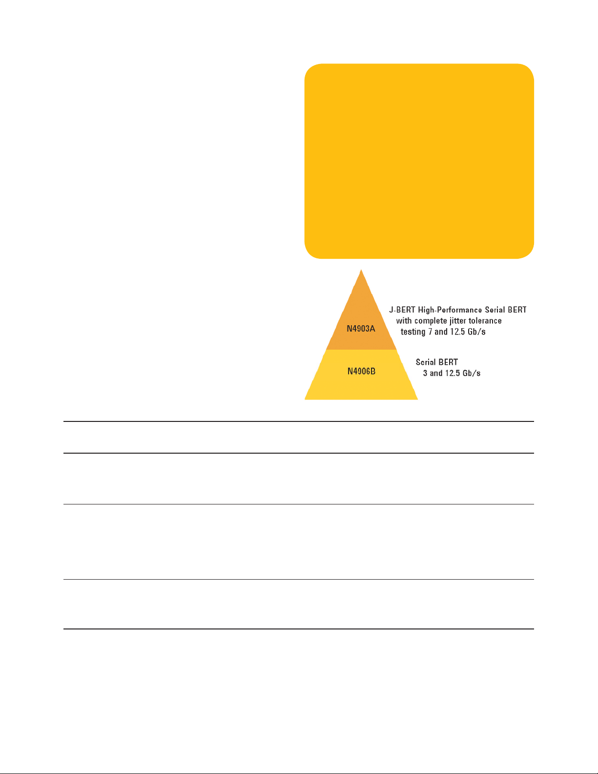
Agilent J-BERT N4903A
High-Performance Serial BERT
with Complete Jitter Tolerance
Testing
7 Gb/s and 12.5 Gb/s
Data Sheet
Smartest Characterization and
Version 3.3
New: Supports optical receiver
stress test
Compliance
Automated jitter tolerance
compliance and characterization
Calibrated jitter composition
Integrated into one box
Compliant to latest serial bus
standards
Key Capabilities:
• Integrated and calibrated jitter sources: PJ, SJ, RJ,
BUJ, ISI and sinusoidal interference
• Jitter tolerance testing: PCI Express
Channel, FB-DIMM, CEI, 10 GbE, XFP/XFI, SFP+
• Quick eye masks and BER contours
• Bit recovery mode for analyzing undeterministic
patterns
• SSC generation
• CDR with tunable loop bandwidth for compliant
measurements for all data rates
• Pattern sequencer and capture to simplify the
handling of complex data patterns
• Subrate clock outputs
• Pattern generator options
• All options upgradable
®
, SATA, Fibre
Agilent Technologies N4900 Series
The newest member of Agilent’s N4900 serial
BERT series is the powerful J-BERT N4903A HighPerformance Serial BERT. It addresses the needs
of R&D and validation teams to characterize serial
I/O ports or ASICs up to 12.5 Gb/s. Integrated and
calibrated jitter sources for jitter tolerance measurements also allow designers to characterize and
prove compliance of their receiver’s jitter tolerance.
The J-BERT N4903A High-Performance Serial
BERT is the ideal choice for characterization. It
offers fully integrated and calibrated jitter tolerance tests integrated in a high-performance BERT.
Agilent’s N4900 serial BERT series offers
key benefits:
• Excellent precision and sensitivity for accurate
measurements
• Choice of feature set and frequency classes to tailor
to test needs and budget
• Pass/Fail testing
• State-of-the-art user interface with color touch
screen
• Remote control via LAN, USB and GPIB interfaces,
compatible with existing command set Agilent 71612,
81630A Series, N4900 Series
• Small form factor saves rack or bench space
The N4906B serial BERT offers an economic BERT
solution for manufacturing and telecom device
testing.
Table 1: Serial BERT applications and selection guide
Device under test Typical requirements Recommended Agilent BERT
For R&D and characterization For manufacturing
Optical transceivers, i.e.: PRBS N4903A N4906B opt. 012
SONET, SDH, Signal precision
10GbE, Eye masks
XFP/XFI, SFP+ Data rates 10 Gb/s
High-speed serial computer Test pattern sequences N4903A* N4906B
buses, and backplanes, i.e. CDR opt. 012/101/102
PCI Express 1.x and 2.0, Differential inputs
SATA II and III, SAS, Datarates < 7 Gb/s
Infiniband-DDR, CEI,
Fibre Channel 4 G/8 G, etc.
0.6 – 2.5 Gb/s transceiver, i.e. Fast bit synchronization N4906B N5980A
E-PON/ G-PON OLTs, Data rates < 3.5 Gb/s opt. 003*
Gigabit Ethernet,
Fibre channel 1x/2x
*or ParBERT 81250
2
J-BERT N4903A High-Performance Serial BERT Data Sheet

J-BERT N4903A High-Performance Serial BERT
The J-BERT N4903A High-Performance Serial
BERT provides the only complete jitter tolerance
test. It is the ideal choice for R&D and validation teams characterizing and stressing chips and
transceiver modules that have serial I/O ports
up to 7 Gb/s or 12.5 Gb/s. It can characterize a
receiver’s jitter tolerance and prove its compliance to today’s most popular standards, such as
PCI Express, SATA, Fibre Channel, Fully Buffered
DIMM, CEI, 10 GbE/ XAUI, XFP/XFI, SFP+.
Accurate characterization is achieved with clean
signals from the pattern generator, which features
exceptionally low jitter and extremely fast transition times. Test set-up time is reduced significantly, because the J-BERT N4903A matches most
recent serial bus standards optimally:
• Undeterministic patterns can now be analyzed
with the bit recovery mode.
• A pattern sequencer helps to set up training
sequences quickly, to get complex devices into
loop-back test mode.
• Reference clocks can be provided by the subrate
clock outputs, which can generate any ratio of
clock to data rate.
• All I/Os are differential and a built-in CDR
allows testing of clockless interfaces.
J-BERT key characteristics:
• 150 Mb/s to 7 Gb/s or 12.5 Gb/s – enough margin for
characterizing today’s most popular serial interfaces
• Calibrated and integrated jitter injection (opt. J10). All
in one box: RJ, PJ, BUJ, ISI, sinusoidal interference to
stress the receiver with > 50 % eye closure
• Automated and compliant jitter tolerance tests covers
popular serial bus standards: PCI Express, SATA, Fibre
Channel, SATA, FB-DIMM, CEI 6G/11G, 10 GbE/XAUI,
XFP/XFI, SFP+
• Delay control input for generator to apply any external
jitter source
• Bit recovery mode to test unknown data traffic
• Pattern sequencer to generate complex training
sequences
• SSC clocking for computer buses
• Subrate clocks to generate reference clocks easily
• Differential I/O for DATA and CLOCK and most supplementary signals for testing serial interfaces
• Integrated CDR (clock data recovery) to test clock-
less devices from 1 to 12.5 Gb/s
• Compliant and tunable loop bandwidth (opt. CTR)
• Highest performance BERT for accurate
measurements
• Remote operation of GUI via web server
• All options retrofitable
The J-BERT N4903A is a future proof serial BERT
platform, which is configurable for today’s test and
budget requirements but also allows upgrades to
all options and full speed.
Available J-BERT Configurations
BERT pattern generator and error detector,
including built-in CDR
BERT 150 Mb/s to 12.5 Gb/s N4903A-C13
BERT 150 Mb/s to 7 Gb/s N4903A-C07
Pattern generator (PG) options
*only in combination with -J10
PG 150 Mb/s to 12.5 Gb/s* N4903A-G13
PG 150 Mb/s to 7 Gb/s* N4903A-G07
SSC clocking* N4903A-J11
Jitter tolerance options
RJ, PJ, SJ, BUJ injection N4903A-J10
ISI and sinusoidal N4903A-J20
interference injection
Jitter tol. compliance suite N4903A-J12
Error detector options
Bit recovery mode N4903A-A01
Compliant CDR N4903A-CTR
with tunable loop bandwidth
Upgrades
All options upgradable (see page 17)
J-BERT N4903A High-Performance Serial BERT Data Sheet
Measurements
BER and measurement suite
• BERT scan
• Output timing jitter
• Spectral jitter decomposition
• Eye contour
• Quick eye diagram and BER contour
• Fast eye mask
• Output level and Q factor
• Error location capture
• Fast total jitter
• Pattern capture
Jitter tolerance tests
• Manual jitter composition (option J10)
• Automated jitter tolerance
• Characterization (option J10)
• Automated jitter tolerance compliance
(option J12)
Applications
• PCI Express
• SATA
• Fibre channel
• Fully buffered DIMM
• CEI
• 10 GbE/XAUI
• XFP/XFI, SFP+
3

Jitter Tolerance Tests
Jitter Tolerance Tests
Calibrated jitter injection
• Periodic jitter (option J10)
• Sinusoidal jitter (option J10)
• Random jitter (option J10)
• Bounded uncorrelated jitter (option J10)
• Intersymbol interference (ISI) (option J20)
• Sinusoidal interference (option J20)
External jitter injection
Using an external source connected to delay
control input.
User Controls
Manual jitter composition (option J10)
of PJ, SJ, RJ, BUJ, ISI and sinusoidal interference.
This screen allows the user to set up combinations of jitter types and jitter magnitudes easily.
Therefore a calibrated ‘stressed eye’ with more
than 50% eye closure can be set up for receiver
testing. Additional jitter can be injected with the
interference channel (option J20). It adds ISI and
differential/single mode noise.
Automated jitter tolerance characterization
(option J10)
Automated sweep over SJ frequency based on the
start/stop frequency, steps, accuracy, BER level,
confidence level and DUT relax time. The green
dots indicate where the receiver tolerated the
injected jitter. The red dots show where the BER
level was exceeded. By selecting a tested point, the
jitter setup condition is restored for further analysis (with SW 4.5 or later). The compliance curve
can be shown on the result screen for immediate
result interpretation (with SW 4.5 or later). This
automated characterization capability saves significant programming time.
Automated jitter tolerance compliance (option J12)
It automatically tests compliance against a receiver’s jitter tolerance curve limits specified by a
standard or the user. Most of the popular serial
bus standards define jitter tolerance curves. This
option includes a library of jitter tolerance curves
for: SATA, Fibre Channel, 10 GbE/XAUI, CEI
6/11 G, and XFP/XFI. Pass/fail is shown on a
graphical result screen, which can be saved and
printed. A comprehensive compliance report,
including the jitter setup and total jitter results for
each test point, can be generated and saved as a
html file for simple jitter tolerance test documentation.
Figure 1: Manual jitter composition. This allows a combination
of jitter types to be injected.
Figure 2: Automated jitter tolerance characterization. The green
circles show where DUT works within the required BER-level.
Figure 3: Result screen of the automated jitter tolerance compliance. A library of jitter tolerance curves is available.
4
J-BERT N4903A High-Performance Serial BERT Data Sheet
User Interface and Measurement Suite
Quick eye diagram and masking
The quick eye diagram allows a one-shot check for
a valid signal. Due to the higher sampling depth of
a BERT, the eye contour lines visualize the measured eye at a deeper BER level for more accurate
results. Extrapolated eye contour lines display the
eye opening for even lower BER levels, such as
-15
10
, reducing the measurement time significantly. The display shows numerical results for
1-/0- level, eye amplitude and width, total jitter
and more. Eye masks can be loaded from a library.
Violations of the captured eye mask are displayed.
The result screen can be printed and saved for
documenting test results (see figure 4).
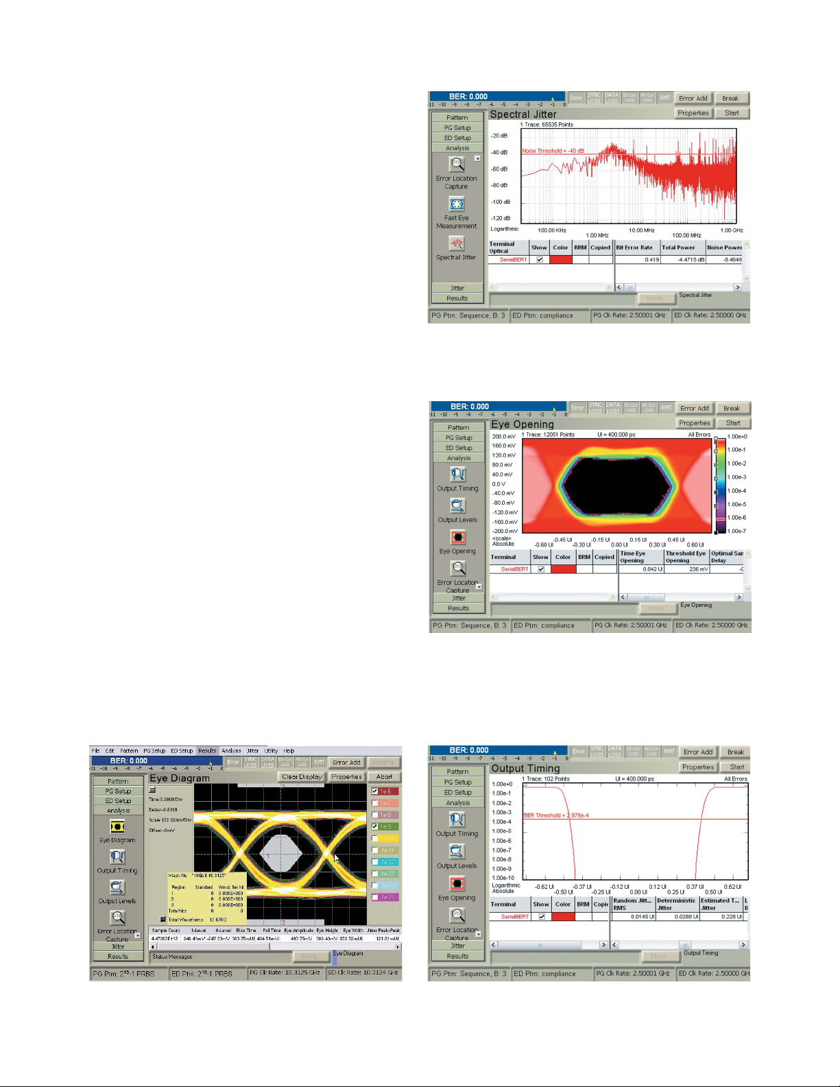
Spectral jitter decomposition
It measures the spectral decomposition of jitter
components. When debugging designs, the jitter
decomposition simplifies identifying deterministic
jitter sources (see figure 5).
Eye contour
The eye opening is a key characteristic of a device.
The BER is displayed as a function of sampling
delay and sampling threshold. Different views are
available: eye contour (see figure 6), pseudo colors
and equal BER plots.
User Interface
Figure 5: Spectral jitter decomposition for debugging jitter
sources in a design.
BERT scan including RJ/DJ separation
This measurement shows the BER versus the sampling point delay, which is displayed as a “bathtub” curve or as a histogram. The measurement
results are displayed in a table with setup and
hold time over phase margin, total jitter in rms or
peak-to-peak, and random and deterministic jitter.
The measurement method is equivalent to IEEE
802.3ae (see figure 7).
Figure 6: Eye contour with colors indicating BER level.
Figure 4: Quick eye diagram with BER contour and masking.
J-BERT N4903A High-Performance Serial BERT Data Sheet
Figure 7: BERT scan including RJ/DJ separation, total jitter.
5

User Interface
Bit recovery mode (option A01)
This mode is useful for analyzing non-deterministic
traffic. This is helpful when you need to analyze
real world traffic, for example in a PCI Express
link where so-called ‘skip ordered sets’ are added
unpredictably to avoid FIFO overflow. This simplifies setup by eliminating the need to setup expected data for the error detector. Two analyzer sampling points are used to measure a relative BER,
which makes the following measurements possible
with relative BER:
BERT scan including RJ/DJ separation
•
Output levels and Q factor
•
Eye contour
•
Fast eye mask
•
Fast total jitter
•
Spectral jitter decomposition
•
Automatic alignment
The J-BERT N4903A High-Performance Serial
BERT is able to align the voltage threshold and the
delay offset of the sampling point automatically,
either simultaneously or separately. It is possible to
search for the 0/1 threshold automatically on command, and to track the 0/1 threshold continuously
(see figure 9).
Figure 8: Bit recovery mode for analyzing non-deterministic
traffic.
Fast total jitter
Agilent implemented a new measurement
technique for TJ (BER), the fast total jitter measurement. This method provides fast and feasible
total jitter measurements, around 40 times faster
than a common BERT scan but with comparable
confidence level. Instead of comparing bits until
the BER reaches a defined number of bits or a
defined number of errors, it only compares bits
until it can decide with a 95% confidence level
whether the actual BER is above or below the
desired BER (see figure 10).
Web-based access to GUI
J-BERT can be operated conveniently from any
remote web location with the built-in web
server (SW 4.5). So even without programming
knowledge, J-BERT can be operated and
monitored from a distance or off-site and in noisy
or environmental test labs.
Figure 9: Auto alignment (center) simplifies correct sampling
even for stressed eyes.
Figure 10: Fast total jitter measurement for quick and
accurate total jitter measurements.
6
J-BERT N4903A High-Performance Serial BERT Data Sheet

Pattern Generator Specifications
Figure 11: Generator connectors on front panel
Data output (DATA OUT)
Table 2: Output characteristics for J-BERT N4903A generator.
All timing parameters are measured at ECL levels.
Range of operation 150 Mb/s to 12.5 Gb/s (opt. C13)
Can be programmed up to
13.5 Gb/s
150 Mb/s to 7 Gb/s (opt. C07)
< 620 MHz only with external
clock
Specifications-Pattern Generator
Pattern generator key characteristics:
• Available as 7 and 12.5 Gb/s pattern generator without error detector (opt. G07 and G13)
• Differential outputs for data, clocks and trigger
• Variable output voltages covering LVDS, ECL, CML
• Transitions times < 20 ps
• Clean pulses with jitter < 9 ps pp
• High precision delay control input to inject jitter from
an external source
• Calibrated and integrated jitter injection
(options J10, J20, both retrofitable)
• Subrate clocks for generating any reference clock
• Pattern sequencing and 32 Mbit pattern
• SSC clocks for computer buses (option J11)
Frequency accuracy ± 15 ppm typical
Format
NRZ, normal or inverted
Amplitude/resolution 0.10 V to 1.8 V, 5 mV steps
Addresses LVDS, CML, PECL,
ECL (terminated to 1.3V/
0 V/-2 V), low voltage CMOS
Output voltage window
Predefined levels ECL, PECL (3.3 V), LVDS, CML
Transition times
(20% to 80%) < 20 ps
(10% to 90%)
Jitter 9 ps pp typical with disabled jitter
sources and internal clock
Clock/data delay range ± 0.75 ns in 100 fs steps
External termination -- 2 V to +3 V
voltage
Crossing point Adjustable 20% to 80% typical to
emulate duty cycle distortions
Single error inject Adds single errors on demand
Fixed error inject Fixed error ratios of 1 error in
10
Interface
DC coupled, 50 Ω
Connector 2.4 mm female
1)
At 10 Gb/s and 7 Gb/s
2)
For positive termination voltage or termination to GND, external
termination voltage must be less than 3 V below VOH. For
negative termination voltage, external termination voltage must
be less than 2 V below VOH. External termination voltage must
be less than 3 V above VOL.
3)
Unused outputs must be terminated with 50Ω to GND.
1)
2)
3)
Differential or single-ended,
-- 2.0 V to +3.0 V
< 25 ps
n
bits, n = 3, 4, 5, 6, 7, 8, 9
Figure 12: Clean output signal. 10 Gb/s, LVDS levels.
Figure 13: Pattern generator setup screen with graphical
display of signal levels.
J-BERT N4903A High-Performance Serial BERT Data Sheet
7
Specifications-Pattern Generator
Clock output (CLK OUT)
Table 3: Clock output characteristics. All timing parameters are
measured at ECL levels.
Frequency range 150 MHz to 12.5 GHz (opt. C13)
Can be programmed up to
13.5 GHz
150 MHz to 7 GHz (opt. C07)
<620 MHz only with external clock
Amplitude/resolution 0.1 V pp to 1.8V pp, 5 mV steps
Output voltage window
Transition times
(20% to 80%) < 20 ps
(10% to 90%)
1)
< 25 ps
External termination -- 2 V to +3 V
2)
voltage
Jitter 1 ps rms typical with disabled jitter
sources and internal clock
SSB phase noise < --75 dBc with internal
clock source, 10 GHz @ 10
kHz offset, 1 Hz bandwidth
Interface
3)
Differential or single-ended,
DC coupled, 50 Ω output
impedance
Connector 2.4 mm female
1)
At 10 Gb/s and 7 Gb/s
2)
For positive termination voltage or termination to GND, external
termination voltage must be less than 3 V below VOH. For
negative termination voltage, external termination voltage
must be less than 2 V below VOH. External termination volt
age must be less than 3 V above VOL.
3)
Unused outputs must be terminated with 50 Ω to GND.
-- 2.00 to + 2.8 V
10 MHz reference input (10 MHz REF IN)
It is used to lock the generator to an external 10 MHz
reference clock. The data rate can be selected within
the same range as if the internal clock would be used.
The provided reference clock must not be modulated.
All internal jitter sources are available.
Table 4: Specifications for clock input and 10 MHz reference input
Amplitude 200 mV to 2 V
Interface AC coupled, 50Ω nominal
Connectors
- Clock input: SMA female, front panel
- 10 MHz reference input: BNC, rear panel
Delay control input (DELAY CTRL IN)
The external signal applied to delay control input, varies
the delay between data output and clock output. This can
be used to generate jittered signals to stress the device
under test in addition to the calibrated jitter injection
from N4903A.
Table 5: Specifications for delay control input
Range -- 100 ps to +100 ps
Sensitivity 400 ps/V typical
Linearity ± 5 % typical
Modulation 1 GHz typical at 10.8 Gb/s
Bandwidth data rate
Levels -- 250 mV to + 250 mV
Interface DC coupled, 50 Ω nominal
Connector SMA female
Error add input (ERROR ADD)
The external error add input adds a single error to the
data output for each rising edge at the input.
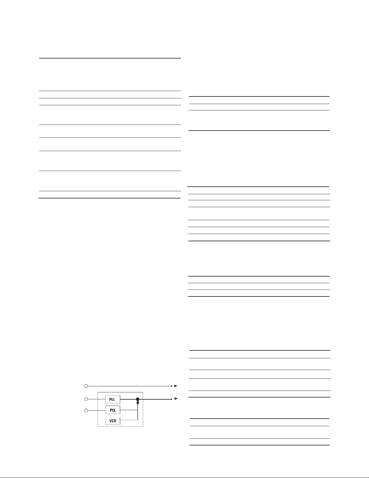
Clock Input (CLK IN)
There are two modes when using the clock input
connector.
External Clock mode: all output signals of the generator follow the external clock and its modulation.
Nevertheless, the modulation of the external clock
must be within the same range given for SSC and
SJ (see tables 11 and 21) or the 500 ps delay line.
When using External Clock mode the internal SSC
and SJ sources and the 500 ps delay line for PJ injection are disabled. Modulation using the
200 ps delay line is still available (see figure 24).
External PLL mode: it is used to lock the generator to
an external clock at the same data rate. The provided
clock must not be modulated in external PLL mode. All
internal jitter sources are available.
External Clock
10 MHz Ref Clock
External Clock
(Ext. PLL mode)
Internal Clock
Clock Generator
Figure 14: N4903A clock modes
Table 6: Specifications for error inject input
Levels TTL compatible
Interface DC coupled, 50 Ω nominal
Connector SMA female
Subrate clock output (SUB CLK OUT)
The subrate clock output is used to generate
reference clocks, which are subrates of the data rate, for
example, a 100 MHz clock for 2.5 or 5 Gb/s PCI Express
data rate.
Table 7: Specifications for subrate clock output
Divider factors n = 2,3…128
Levels High: + 0.5 V
Low: -- 0.5 V typical
Transition times 35 ps typical
Interface DC coupled, 50 Ω differential
or single-ended
Connector SMA female
10 MHz Reference output (10 MHZ REF OUT)
Table 8: Specifications for the 10 MHz reference output
Amplitude 1V into 50 Ω typical
Interface AC coupled,
50 W output impedance
Connector BNC, rear panel
8
J-BERT N4903A High-Performance Serial BERT Data Sheet

Specifications-Pattern Generator
Trigger outputs (TRIGGER OUT)
This provides a trigger signal synchronous with
the pattern, for use with an oscilloscope or other
test equipment. Typically there is a delay of 32 ns
between trigger and data output for data rates ≥
620 Mb/s. The trigger output has two modes.
Pattern trigger mode: for PRBS patterns; the pulse
is synchronized with a user specified trigger pattern. One pulse is generated for every 4th PRBS
pattern.
Divided clock mode: the trigger is a square wave
with the frequency of the clock rate divided by 2, 4,
8, 10, 16, 20, 32, 64, and 128.
Table 9: Specifications for trigger output
Pulse width Square wave
Transition times 35 ps typical
Levels High: +0.5 V; Low -- 0.5 V typ.
Interface DC coupled, 50 Ω nominal,
single ended or differential
Connector SMA female
AUX input (AUX IN)
When the alternate pattern mode is activated, the
memory is split into two parts, and the user can
define a pattern for each part. Depending on the
operating mode of the auxiliary input, the user can
switch the active pattern in real time by applying
a pulse (mode 1) or a logical state (mode 2) to the
auxiliary input. If the alternate pattern mode is not
activated, the user can suppress the data on the
data output by applying a logical high to the auxiliary input (mode 3).
Patterns
PRBS: 2n-1 with n = 7, 10, 11, 15, 23, 31,
and 2n with n = 7, 10, 13, 15, 23, 31.
User definable pattern: 32 Mbit, independent for
pattern generator and error detector.
Generator pattern sequencing
The generators pattern sequences can be started
on command or by a signal applied to the auxiliary
input.
Number of blocks: up to 4; the block resolution of
user definable pattern is 512 bits.
Loops: over 4 or fewer blocks, 1 loop level, loop
counter and infinite.
Figure 15: Pattern generator sequencer helps to set up
complex training sequences.
Table 10: Specifications for auxiliary input
Levels TTL compatible
Interface DC coupled, 50 Ω nominal
Connector SMA female
SSC – spread spectrum clocking (option J11)
The built-in SSC clock modulation source is available only in combination with option J10.
It generates a frequency modulated clock signal
as used in some computer storage standards to
spread EMI. If spread spectrum clocking is enabled, sinusoidal jitter is disabled, however all other
jitter sources can be used.
Table 11: Spread spectrum clocking (SSC) characteristics
Frequency deviation 0 to --0.5%, (5000 ppm)
2% typical accuracy
Modulation frequency 28 kHz to 34 kHz
Waveform Triangle
Signals impacted Subrate clock output,
data output, clock output,
trigger output
J-BERT N4903A High-Performance Serial BERT Data Sheet
Alternate pattern
This allows switching between two patterns of
equal length that have been programmed by
the user, each of which can be up to 16 Mbit.
Switching is possible using a front panel key, over
GPIB or by applying the appropriate signal to the
auxiliary input port. Changeover occurs at the end
of the pattern. The length of the alternating patterns should be a multiple of 512 bits. Two methods of controlling pattern changeover are available: one-shot and alternate.
Zero substitution
Zeros can be substituted for data to extend the
longest run of zeros in the patterns listed below.
The longest run can be extended to the pattern
length-1. The bit following the substituted zeros is
set to 1.
Variable mark density
The ratio of ones to total bits in the predefined
patterns listed below can be set to 1/8, 1/4, 1/2,
3/4, or 7/8.
Library of predefined patterns
Display Port, FDDI, Fibre Channel, K28.5, SAS,
SATA, SDH, SONET.
9

Specifications-Error Detector
Error Detector Specifications
Clock inputs (CLK IN)
The error detector requires an external clock
signal to sample data or it can recover the clock
from the data signal using the built-in clock data
recovery (CDR).
Table 13: Specification for the clock input
Frequency range 150 MHz to 12.5 GHz
(option C13)
150 MHz to 7 GHz
(option C07)
Figure 16: Front panel connectors for error detector
Amplitude 100 mV to 1.2 V
Sampling
clock edge
Error detector key characteristics:
Interface AC coupled, 50 Ω nominal
Connector SMA female
• True differential inputs to match today’s ports
• Built-in CDR for clockless data
• Auto-alignment of sampling point
• Bit recovery mode for unknown data traffic
(option AO1)
• Burst mode for testing recirculation loop
• BER result and measurement suite
• Quick eye diagram and mask with BER contours
• Pattern capture
• CDR with tunable loop bandwith (option CTR)
Clock data recovery
The error detector can recover the clock from the
incoming data stream with the built-in clock data
recovery (CDR). The CDR with fixed loop bandwidth is included in options C07 and C13. The
tunable loop bandwidth is available with N4903A
option CTR. For upgrading an existing J-BERT to
the compliant and tunable CDR loop bandwidth
option UTR is available.
Data inputs (DATA IN)
Table 12: Specifications for error detector
Range of operation 150 Mb/s to 12.5 Gb/s
(opt. C13)
150 Mb/s to 7 Gb/s
(opt. C07)
Format NRZ
Maximum input amplitude
Termination voltage
(true differential mode)
Sensitivity
2)
<50 mV pp
Intrinsic transition time
single ended
Decision threshold range -- 2 V to +3 V in 1 mV steps
Maximum levels -- 2.2 V to + 3.2 V
Phase margin
4)
1 UI – 12 ps typical
Clock/Data sampling delay ±0.75 ns in 100 fs steps
Interface Single-ended: 50 Ω nominal,
Differential: 100 Ω nominal
Connector 2.4 mm female
1)
Selectable 2 V operating voltage window, which is in the
range between -- 2.0 V to +3.0 V. The data signals, termination
voltage and decision threshold have to be within this voltage
window.
2)
At 10 Gb/s, BER 10
manual threshold value adjustments may be required.
3) At cable input, @ ECL levels.
4)
Based on the internal clock.
2.0 V
1)
-- 2 V to + 3 V or off
3)
25 ps typical 20% to 80%,
-12
, PRBS 231-1. For input levels <100 mV
The recovered clock signal is available at the aux
output.
Table 14: Specifications for the clock data recovery (options C07,
C13, CTR, UTR)
Input data rate
1 Gb/s to 7 Gb/s (option C07)
CDR clock output jitter 0.01 UI rms (RJ) typical
Fixed loop bandwidth data rate: 1667; see figure 17
1)
With bit recovery mode (option A01) enabled the max. data rate
is 11.5 Gb/s.
2)
When measured with PRBS 2
3)
For J-BERTs with serial number DE45Axxxxx which have not
been upgraded to option UTR, the CDR operates in these rang
es (loop bandwidth, typical):
9.20 Gb/s to 11.32 Gb/s (8 MHz)
4.23 Gb/s to 6.40 Gb/s (4 MHz)
2.115 Gb/s to 3.20 Gb/s (2 MHz)
1.058 Gb/s to 1.60 Gb/s (1MHz)
Positive or negative
3)
1 Gb/s to 12.5 Gb/s 1) (option C13)
23
-1
2)
10
J-BERT N4903A High-Performance Serial BERT Data Sheet
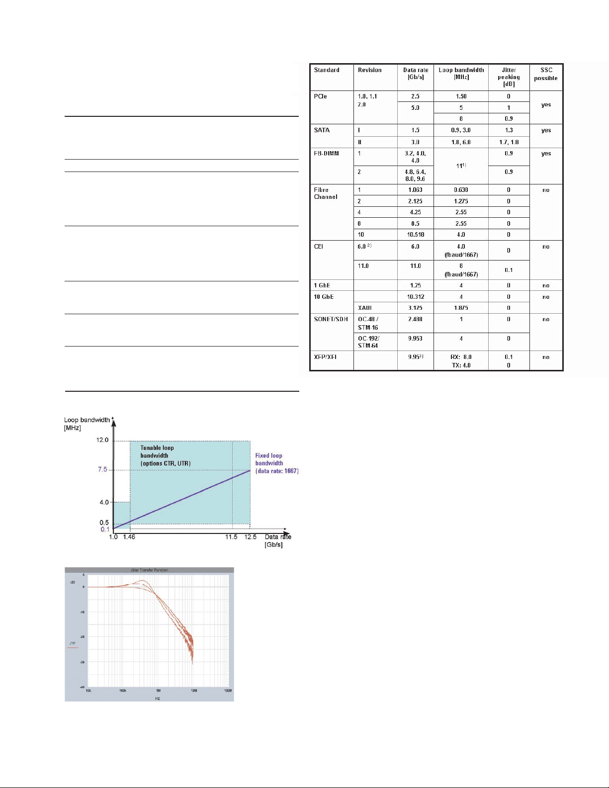
CDR with tunable loop bandwidth
(only with N4903A options CTR, UTR)
Table 15: Specifications for tunable loop bandwidth (only for
option CTR, UTR)
Tunable loop bandwidth 500 kHz to 12 MHz for data rates
1.46 Gb/s to 12.5 Gb/s
100 kHz to 4 MHz for data rates
1 Gb/s to 1.46 Gb/s
Loop bandwidth accuracy 10% typical
Transition density 25% to 100%. The CDR can autocompensation matically detect the transition den-
sity of the incoming data pattern
and compensates the loop band
width accordingly.
Tracking range (SSC) + 0.05 % to -0.55% (5500 ppm)
deviation of data rate. User can
disable/enable SSC tracking. Loop
bandwidth >1 MHz and medium or
max. peaking enabled.
Jitter peaking 3 customer selectable values
between 0 and 3 dB; see
frequency response in figure 18.
Fine adjust Manual adjustment -1.0 to + 1.0 of
CDR settings to minimize CDR
output jitter.
Compliant CDR settings PCIe, SATA, FC, FB-DIMM, CEI,
GE,10 GbE, XAUI, XFP/XFI, SONET
OC-48/192 (see figure 19). User
can add own CDR settings.
1)
At transition density 50%
1)
Specifications-Error Detector
Figure 19: Compliance settings for CDR
1)
The standard allows 11 MHz to 22 MHz.
2)
CEI standard allows data rates of 4.976 to 6.375 Gb/s and 9.95
to 11.1 Gb/s.
3)
XFP/XFI standard allows data rates of 9.95 to 11.2 Gb/s.
Figure 17: CDR loop bandwidth
Figure 18: Three selectable frequency response settings. The
example shows loop bandwidth of 900 kHz and 0 dB, 1.2 dB,
2.8 dB peaking.
BER result display
The N4903A error detector measures:
1. BER
2. Accumulated BER results
• Accumulated errored O’s and 1’s
• G.821
• Error-free intervals
• Accumulated parameters
• Burst results
3. Eye results
Eye diagram result display
• 1-/0- level
• Eye height/amplitude/width
• Jitter p-p and rms
• Cross voltage
• Signal to noise ratio
• Duty cycle distortion
• Extinction ratio
J-BERT N4903A High-Performance Serial BERT Data Sheet
11

Specifications-Error Detector
Trigger output (TRIG OUT)
Gating input (GATE IN)
If a logical high is applied to the gating input the
Pattern trigger mode
This provides a trigger synchronized with the
selected error detector reference pattern. In pattern mode the pulse is synchronized to repetitions
of the output pattern. It generates 1 pulse for every
4th PRBS pattern.
analyzer will ignore the incoming bits during a
BER measurement. The ignored bit sequence is a
multiple of 512 bits. For measuring data in bursts
of bits, rather than a continuous stream of bits, a
special operating mode is used. This is the burst
sync mode. In this case, the signal at the gating
input controls the synchronization and the error
Divided clock mode
counting for each burst.
In divided clock mode, the trigger is a square wave.
Table 16: Specifications for trigger output
Clock divider 4, 8, 16 up to 11 Gb/s
32, 40, 64, 128 up to 12.5 Gb/s
Levels High: +0.5 V typical
Low: --0.5 V typical
Minimum pulse width
e.g. 10 Gb/s with 1000 bits = 50 ns
Interface
Connector SMA female
Pattern length x clock period/2
DC coupled, 50 Ω nominal
Error output (ERR OUT)
This provides a signal to indicate received errors.
The output is the logical ‘OR’ of errors in a 128 bit
segment of the data.
Table 17: Specifications for error output
Interface format RZ, active high
Levels High: 1 V typical
Low: 0 V typical
Pulse width
Interface
Connector SMA female
128 clock periods
DC coupled, 50 Ω nominal
Data Input
Gate Input
Figure 20: Burst mode allows recirculation loop testing.
This is an important feature for recirculation loop
measurements. If clock data recovery (CDR) is
used to recover the clock from the burst data, the
CDR takes 2 µs from the start of the burst data to
settle. The number of bits needed to synchronize
itself during a burst depends on whether the pattern consists of hardware based PRBS data or
memory based data. To run properly in burst mode
the system needs a backlash of data after the gating input returns to high. During each burst, the
gating input has to remain passive.
CDR Settling Time
Sync. Time
Backlash
Checked Data
Burst
High
Low
Auxiliary output (AUX OUT)
This output can be used to provide either clock or
data signals:
Clock: clock signals from the input or the recovered clock signals in CDR mode.
Data: weighted and sampled data.
Table 18: Specifications for the auxiliary output
Amplitude 600 mV typical
Interface AC coupled, 50 Ω nominal
Connector
12
SMA female
J-BERT N4903A High-Performance Serial BERT Data Sheet
Table 19: Specifications for gating input
Burst synchronization time 1536 bits for PRBS
15 kbit for pattern
Backlash 1536 bits in non-CDR mode
1.5 µs in CDR-mode
Gate passive time
2560 bits or 1.5 µs whichever
is longer, in CDR-mode
Interface levels TTL levels
Pulse width 256 clock periods
Connector SMA female
2560 bits in non-CDR mode
Pattern capture
The error detector can capture up to 32 MB data
bits from the device under test. The captured data
bits are displayed in the pattern editor in hex or
binary format. The data bits can be used as expected data for BER testing or can be saved for post
processing.

Jitter Tolerance Test Specifications
The built-in jitter sources are designed to cover
PCI Express, SATA, Fibre channel, FB-DIMM, CEI 6
G/11 G, 10 GbE and XFP/XFI, SFP+ jitter tolerance
test needs. If jitter sources are enabled, the intrinsic
jitter at the pattern generators clock and data outputs is 1.4 ps rms typical.
Periodic jitter (option J10)
This injects sinusoidal, rectangular or triangular jitter over
a wide frequency range.
Specifications-Jitter Tolerance Test
Figure 22: Periodic jitter maximum for datarates ≤ 3.375 Gb/s
using the 500 ps delay line.
Table 20: Specifications for periodic jitter (PJ)
1)
Range
0 to 500 ps pp @ datarates
≤ 3.375 Gb/s
Modulation 1 kHz to 300 MHz sinewave
frequency 1 kHz to 20 MHz triangle
1 kHz to 20 MHz square wave
Modulation frequency 0.5% ± 25 Hz typical
accuracy
Jitter amplitude
accuracy
Signals impacted Data outputs: for all datarates
subrate clock outputs, for
datarates ≤ 3.375 Gb/s when
using 500 ps delay line
1)
rate (see figure 21 and 22)
0 to 200 ps pp @ all datarates
10% ± 1ps typical
Available range depends on modulation frequency and data
Sinusoidal jitter (option J10)
This injects sinusoidal jitter in
the lower frequency range with
multiple UIs.
Table 21: Specifications for sinusoidal jitter (SJ)
1)
Range
1000 UI @ 10 kHz
2 UI @ 5 MHz
For frequencies between 10 kHz
and 5 MHz the jitter amplitude
10 MHz
n x f (mod)
Modulation 100 Hz to 5 MHz
frequency (For higher modulation
frequencies see table 20 and 21.)
Modulation frequency 0.5% typical
accuracy
Jitter amplitude 2% ± 1ps typical
accuracy
Signals impacted Data and subrate clock outputs.
User selectable: all pattern
generator output (data,clock,
subrate clock and trigger outputs.)
=
UI
Figure 21: Periodic jitter maximum for all data rates using the
200 ps delay line.
J-BERT N4903A High-Performance Serial BERT Data Sheet
1)
Available range depends on modulation frequency and data rate
(see figure 23).
Figure 23: Sinusoidal jitter maximum UI
13

Specifications-Jitter Tolerance Test
Random jitter (option J10)
This injects random jitter with a
high bandwidth and excellent
crest factor.
Table 22: Specifications for random jitter (RJ)
Range 0 to 14 ps rms
Crestfactor 14 (pp to rms ratio)
Bandwidth 50 kHz to 1 GHz
Filter
10 MHz high-pass
500 MHz low-pass
Can be turned on/off individually
to limit jitter bandwidth.
Jitter amplitude 10% ± 0.2 ps typical
accuracy
Bounded uncorrelated jitter (option J10)
This injects a high probability
jitter using a PRBS generator
and low-pass filters.
Table 23: Specifications for bounded uncorrelated jitter (BUJ)
Range 0 to 200 ps pp @ all datarates
PRBS polynomials 2
Data rate of PRBS
generator
Filters 20/50/100/200 MHz lowpass 3rd order
Jitter amplitude 10% ± 1 ps typical for settings shown in
accuracy table 24.
200 Mb/s to 3.2 Gb/s
n
-1; n = 7, 8, 9, 10, 11, 15, 23, 31
Table 24: BUJ accuracy applies for these BUJ calibration settings.
BUJ calibration datarate for PRBS filter
setting PRBS generator
CEI 6G 1.1 Gb/s PRBS 2
CEI 11G 2 Gb/s PRBS 2
Gaussian 2 Gb/s PRBS 2
Note: Other settings are not calibrated and do not necessarily generate the desired jitter histograms for all datarates of the PRBS generator.
9
-1 100 MHz
11
-1 200 MHz
31
-1 100 MHz
Total jitter
A combination of internally generated PJ, RJ, BUJ
and external jitter (injected using external delay
control input) is possible:
For all datarates: RJ + PJ + BUJ + external delay
control input: total delay variation is
200 ps pp max.
For datarates ≤ 3.375 Gb/s: A 200 ps delay line or
a 500 ps delay line can be used.
If the 500 ps delay line is used: only PJ or only SJ
or only SSC can be injected.
Total delay variation for periodic jitter is shown in
figure 21.
Total delay variation is 200 ps max. for RJ + external delay control input.
Figure 24: Overview of jitter injection capabilities
14
J-BERT N4903A High-Performance Serial BERT Data Sheet
[1]: When 500 ps delay line is used for PJ, additional SSC,
SJ and BUJ is not available. The 200ps delay can be used in
addition, see above for maximum available total jitter.
[2]: When using Automated Characterization/ Compliance:
sinusoidal jitter sweep is generated by SJ and PJ (200 ps
delay line). Additional PJ or SJ cannot be injected. SSC can
be enabled (requires SW rev. 4.5 or later). With SSC enabled
only PJ (200ps delay line) is used for jitter sweep.
[3]: When using CLK IN (external) SSC, SJ and 500 ps delay
line are not available. It is possible to inject a modulated
external clock which must not exceed J-BERT‘s built-in jitter
injection capabilities for SSC/SJ or the 500 ps delay line.
Interference channel (option J20)
The option J20 is only available in addition to
option J10. It includes the semi-rigid cable set to
connect data outputs to P1and P1 (N4915A-002).
Figure 25: Interference channel connectors
Specifications-Jitter Tolerance Test
Figure 26: Typical S21 parameter for ISI channel of 9 inch length.
Interference channel input and output (P1, P2)
User selectable board traces are
switched into the signal path to
emulate a backplane.
Table 25: Specifications for intersymbol interference (ISI)
Trace length 3.5” (minimum), 9” (minimum with
S.I. enabled) 16”, 20”, 24”, 28”, 32”,
36”, 40”, 44” inches of board trace type
Nelco 4000-6. When using in
combination with sinusoidal interfer ence, minimum trace length is 9 inches.
S
parameter See figure 26
21
Range See figure 27
Max. input levels -- 5 .5 V to +5.5 V
Connectors 2.4 mm, female
Sinusoidal interference (option J20)
This adds common mode, differential or single-ended sinewave signal on top of the data
outputs, to test common mode
rejection of a receiver and to
emulate vertical eye closure.
Sinusoidal interference is injected before the signal passes through the ISI board
traces (“near end”) when using P1 as input. For
“far end” injection P2 has to be used as input.
Table 26: Specifications for sinusoidal interference (SI)
Amplitude
ended and differential (differential
amplitude 0 to 800 mV)
Frequency 10 MHz to 3.2 GHz in 100 kHz steps
Level accuracy ± 10 % ±10 mV typical
1)
The output signal amplitude is reduced by 3 dB when sinusoidal
interference is enabled.
1)
0 to 400 mV common mode, single
Figure 27: Typical ISI (measured in UI) for traces depending on datarate, pattern and trace length.
J-BERT N4903A High-Performance Serial BERT Data Sheet
15

Mainframe Characteristics
Table 27: General mainframe characteristics
Operating temperature 5 °C to 40 °C
Storage temperature - 40°C to +70 °C
Operating humidity
non-condensing
Storage humidity 50% rel. humidity
Power requirements 100 to 240 V, ±10%,
47 to 63 Hz, 450 VA
Physical dimensions Width: 424.5 mm
Height: 221.5 mm
Depth: 580.0 mm
Weight (net) 26 kg
Weight (shipping) (max) 37.5 kg
Recommended 1 year
re-calibration period
Warranty period 1 year return to Agilent.
See order instructions for
extended warranty.
95% rel. humidity,
Display
8” color LCD touch screen
Data entry
Color touch screen display, numeric keypad
•
with up/down arrows, dial-knob control or
external key board and mouse via USB interface
Pattern export/import
•
Hard disk
For local storage of user patterns and data. An
external disk is also available for using over the
USB interface.
Removable storage
Floppy Disk Drive 1.44 MB
Remote control interfaces
GPIB (IEEE 488), LAN, USB 2.0.
Language: SCPI, IVI.COM. SCPI commands can be
exported via copy/paste from the utility menu/output window.
Built-in web server: provides remote GUI access
and control of J-BERT via a standard Java enabled
web browser on your computer. (Requires SW 4.5
or higher.)
Figure 28: Rear panel view
IO libraries
Agilents IO libraries suite ships with the N4903A
to help quickly establish an error-free connection
between your PC and instruments regardless of the
vendor.
Other interfaces
Parallel printer port, 2 x LAN, VGA output, 4 x USB
2.0, 1 x USB 1.1 (front).
Operating system
Microsoft Windows XP Professional
Regulatory standards
Safety: IEC 61010-1:2001
EN 61010-1:2001
CAN/CSA-C22.2 No.61010-1-04
UL 61010-1:2004
EMC: EN 61326:1997 + A1:1998 + A2:2001
IEC 61326:1997 + A1:1998 + A2:2000
Quality management: ISO 9004
Specification assumption
The specifications in this brochure describe the
instrument’s warranted performance. Non-warranted values are described as typical.
All specifications are valid in a range from 5 °C to
40 °C ambient temperature after a warm-up phase
of 30 minutes. If not otherwise stated, all inputs
and outputs need to be terminated with 50 Ω to
ground. All specifications, if not otherwise stated,
are valid using the recommended cable set N4910A
(2.4 mm, 24” matched pair).
16
J-BERT N4903A High-Performance Serial BERT Data Sheet

Order Instructions
J-BERT N4903A High-Performance Serial BERT
Includes 5x 50 SMA terminations, 6x adapter
SMA female to 2.4 mm male, USB cable, commercial
calibration report and certificate (“UK6”), getting
started guide, Agilent I/O library.
BERT with built in CDR
J-BERT Options
Data rate 150 Mb/s to 12.5 Gb/s
150 Mb/s to 7 Gb/s
N4903A
-C13
-C07
Jitter tolerance options RJ,PJ,SJ,BUJ injection -J10
SSC generation* -J11
Interference channel* (includes short
cable kit N4915A-002)
Jitter tolerance compliance suite* -J12 ---
Analyzer capabilities Bit recovery mode -A01 ---
Tunable loop bandwidth CDR -CTR ---
* only with opt. J10
Upgrades for J-BERT N4903AU
Data rate To 12.5 Gb/s BERT from 7 Gb/s BERT -U13 ---
Jitter tolerance options RJ,PJ,SJ,BUJ injection (requires recali-
bration at Agilent)
SSC generation -U11
Interference channel -J20
Jitter tolerance compliance suite -U12 ---
Analyzer capabilities To bit recovery mode -U01 ---
To tunable loop bandwidth -UTR ---
To 7 G BERT from 7 G PG --- -UE7
To 12.5 G BERT from 12.5 G PG --- -UED
Pattern Generator
N4903A
-J20
-U10
-G13
-G07
Warranty/Calibration/Productivity Services
Warranty 1 year return-to-Agilent warranty R-51B-001-C
1 year return-to-Agilent warranty
R-51B-001-3C
extended to 3 years
Calibration Agilent calibration upfront support
R-50C-011-3
plan 3 year coverage
Productivity Productivity assistance, remote or
R1380-N49xx PS-S20 and PS-S20-02
on-site
J-BERT N4903A High-Performance Serial BERT Data Sheet
17
Order Instructions Continued
Recommended Accessories
Cables, adapters 2.4 mm matched pair cable N4910A
One adapter 3.5 mm (f) to 2.4 mm(m) N4911A-002
50 Ohm termination, 2.4 mm N4912A
Short cable kit, 2.4 mm(m) to 2.4 mm(m)
for ISI ports
Clock cable, 2.4 mm to SMA N4915A-003
One 2.4 mm cable N4915A-004
Serial bus switch 6.5 Gb/s N4915A-005
Signal/stress conditioning De-emphasis signal converter N4916A
Optical receiver stress test N4917A
One 47 ps transition time converter N4915A-001
Software Test automation software platform N5990A
Rack Rack-mount kit N4914A-FG
N4915A-002
Figure 29: Clock cable N4915A-003
Figure 30: Short cable kit for connecting ISI ports. N4915A-002
Figure 31: De-emphasis signal converter N4916A
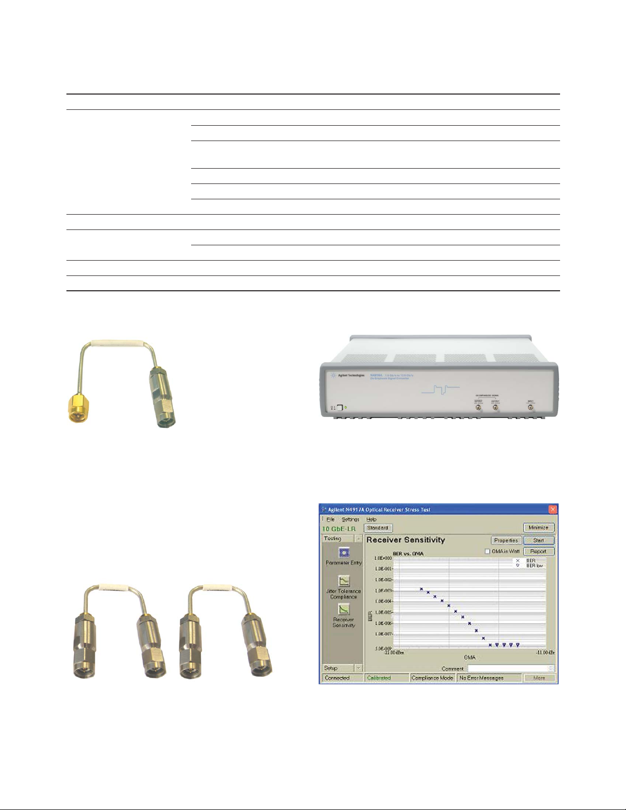
Figure 32: Optical receiver stress testing with N4917A
allows calibrated stressed receiver sensitivity tests
18
J-BERT N4903A High-Performance Serial BERT Data Sheet

J-BERT N4903A High-Performance Serial BERT Data Sheet
19

Related Literature Pub. No.
www.agilent.com
J-BERT N4903A High-Performance Serial BERT 5989-3882EN
Brochure
Bit Recovery Mode for characterizing idle 5989-3796EN
and framed data traffic
Application Note
Calibrated Jitter, Jitter Tolerance Test and Jitter 5989-4967EN
Laboratory with the J-BERT N4903A
Application Note
Mastering jitter characterization with J-BERT & DCA-J 5989-4823EN
Poster
Second Generation PCI EXPRESS
with the N4903A High-Performance Serial BERT
Application Note
N4906B Serial BERT 3 and 12.5 Gb/s 5989-2406EN
Data sheet
Agilent Physical Layer Test 5988-9514EN
Brochure
ParBERT 81250 5968-9188E
Product Overview
86100 Infiniium DCA-J 5989-0278EN
Data Sheet
Infiniium 80000 Series 5989-1487ENUS
Oscilloscopes
Data Sheet
Fast Total Jitter Solution
Application Note
®
Testing 5989-4087EN
5989-3151EN
Remove all doubt
Our repair and calibration services will get your equipment back
to you, performing like new, when promised. You will get full
value out of your Agilent equipment throughout its lifetime.
Your equipment will be serviced by Agilent-trained technicians
using the latest factory calibration procedures, automated repair
diagnostics and genuine parts. You will always have the utmost
confidence in your measurements.
Agilent offers a wide range of additional expert test and measurement services for your equipment, including initial start-up
assistance onsite education and training, as well as design, system integration, and project management.
For more information on repair and calibration services, go to:
www.agilent.com/find/removealldoubt
Agilent Direct
www.agilent.com/find/agilentdirect
Quickly choose and use your test equipment solutions with
confidence.
For more information on Agilent Technologies’ products, applications or services, please contact your local Agilent office. The
complete list is available at:
www.agilent.com/find/contactus
N5990A Test Automation Software Platform 5989-5483EN
Data Sheet
De-Emphasis Signal Converter 5989-6062EN
Data Sheet
Optical Receiver Stress Test 5989-6315EN
Data Sheet
www.agilent.com/find/j-bert
Product specifications and descriptions in this document
are subject to change without notice.
For the latest version of this document, please visit our website
at www.agilent.com/find/j-bert and go to the Key Library
Information and insert the publication number (5989-2899EN)
into the search engine.
Agilent Email Updates
www.agilent.com/find/emailupdates
Get the latest information on the products and applications you
select.
www.agilent.com/find/open
Agilent Open simplifies the process of connecting and programming test systems to help engineers design, validate and manufacture electronic products. Agilent offers open connectivity for a
broad range of system-ready instruments, open industry software,
PC-standard I/O and global support, which are combined to more
easily integrate test system development.
Phone or Fax
United States: China:
(tel) 800 829 4444 (tel) 800 810 0189
(fax) 800 829 4433 (fax) 800 820 2816
Europe: Japan:
(tel) 31 20 547 2111 (tel) (81) 426 56 7832
Korea: (fax) (81) 426 56 7840
(tel) (080) 769 0800 Latin America:
(fax) (080) 769 0900 (tel) (305) 269 7500
Other Asia Pacific Countries: Taiwan:
(tel) (65) 6375 8100 (tel) 0800 047 866
(fax) (65) 6755 0042 (fax) 0800 286 331
Email: tm_ap@agilent.com
Revised: 09/14/06
© Agilent Technologies, Inc. 2007, 2005
Printed in USA, November 21st 2007
5989-2899EN
If you want to learn more about jitter, please visit our website:
www.agilent.com/find/jittermaster
® PCI Express is a registered trademark of PCI-SIG.
 Loading...