

Page 1

Keysight B4623 LPDDR Bus
Decoder
User’s Guide
Page 2

Notices
CAUTION
WARNING
© Keysight Technologies 2013-2014
No part of this manual may be reproduced in
any form or by any means (includ ing electronic storage and retrieval or translation
into a foreign language) without prior agreement and written consent from Keysight
Technologies as governed by United States
and international copyright laws.
Software Release
06.00.0000
Edition
August 2014
Available in electronic format only
Keysight Technologies
1900 Garden of the Gods Road
Colorado Springs, CO 80907 USA
Warranty
THE MATERIAL CONTAINED IN THIS
DOCUMENT IS PROVIDED "AS IS," AND IS
SUBJECT TO BEING CHANGED, WITHOUT
NOTICE, IN FUTURE EDITIONS. FURTHER,
TO THE MAXIMUM EXTENT PERMITTED BY
APPLICABLE LAW, KEYSIGHT DISCLAIMS
ALL WARRANTIES, EITHER EXPRESS OR
IMPLIED WITH REGARD TO THIS MANUAL
AND ANY INFORMATION CONTAINED
HEREIN, INCLUDING BUT NOT LIMITED TO
THE IMPLIED WARRANTIES OF
MERCHANTABILITY AND FITNESS FOR A
PARTICULAR PURPOSE. KEYSIGHT SHALL
NOT BE LIABLE FOR ERRORS OR FOR
INCIDENTAL OR CONSEQUENTIAL
DAMAGES IN CONNECTION WITH THE
FURNISHING, USE, OR PERFORMANCE OF
THIS DOCUMENT OR ANY INFORMATION
CONTAINED HEREIN. SHOULD KEYSIGHT
AND THE USER HAVE A SEPARATE WRITTEN
AGREEMENT WITH WARRANTY TERMS
COVERING THE MATERIAL IN THIS
DOCUMENT THAT CONFLICT WITH THESE
TERMS, THE WARRANTY TERMS IN THE
SEPARATE AGREEMENT WILL CONTROL.
Technology Licenses
The hardware and/or software described in
this document are furnished under a license
and may be used or copied only in accordance with the terms of such license.
52.227-14 (June 1987) or DFAR
252.227-7015 (b)(2) (November 1995), as
applicable in any technical data.
Safety Notices
A CAUTION notice denotes a hazard. It
calls attention to an operating procedure, practice, or the like that, if not
correctly performed or adhered to,
could result in d amage to the prod uct
or loss of important data. Do not proceed beyond a CAUTION notice until
the indicated conditions are fully
understood and met.
A WARNING notice denotes a hazard.
It calls attention to an operating procedure, practice, or the like that, if not
correctly performed or adhered to,
could result in personal injury or
death. Do not proceed beyond a
WARNING notice until the indicated
conditions are fully understood and
met.
Restricted Rights Legend
If software is for use in the performance of a
U.S. Government prime contract or subcontract, Software is delivered and licensed as
"Commercial computer software" as defined
in DFAR 252.227-7014 (June 1995), or as a
"commercial item" as defined in FAR
2.101(a) or as "Restricted computer software" as defined in FAR 52.227-19 (June
1987) or any equivalent agency regulation or
contract clause. Use, duplication or disclosure of Software is subject to Keysight Technologies’ standard commercial license
terms, and non-DOD Departments and
Agencies of the U.S. Government will receive
no greater than Restricted Rights as defined
in FAR 52.227-19(c)(1-2) (June 1987). U.S.
Government users will receive no greater
than Limited Rights as defined in FAR
2 B4623 LPDDR Bus Decoder User’s Guide
Page 3

Safety Summary
CAUTION
WARNING
General Do not use this product in any manner not specified by the manufacturer. The protective features of
The following general safety precautions must be observed during all phases of operation of this
instrument. Failure to comply with these precautions or with specific warnings or operating
instructions in the product manuals violates safety standards of design, manufacture, and intended
use of the instrument. Keysight Technologies assumes no liability for the customer's failure to comply
with these requirements. Product manuals are provided with your instrument on CD-ROM and/or in
printed form. Printed manuals are an option for many products. Manuals may also be available on
the Web. Go to www.keysight.com and type in your product number in the Search field at the top of
the page.
this product may be impaired if it is used in a manner not specified in the operation instructions.
Before Applying
Power
Ground the
Instrument
Fuses See the user's guide or operator's manual for information about line-fuse replacement. Some
Do Not Operate in
an Explosive
Atmosphere
Do Not Remove the
Instrument Cover
Cleaning Clean the outside of the instrument with a soft, lint-free, slightly dampened cloth. Do not use
Do Not Modify the
Instrument
Verify that all safety precautions are taken. Make all connections to the unit before applying power.
Note the instrument's external markings described in “Safety Symbols”.
If your product is provided with a grounding type power plug, the instrument chassis and cover must
be connected to an electrical ground to minimize shock hazard. The ground pin must be firmly
connected to an electrical ground (safety ground) terminal at the power outlet. Any interruption of
the protective (grounding) conductor or disconnection of the protective earth terminal will cause a
potential shock hazard that could result in personal injury.
instruments contain an internal fuse, which is not user accessible.
Do not operate the instrument in the presence of flammable gases or fumes.
Only qualified, service-trained personnel who are aware of the hazards involved should remove
instrument covers. Always disconnect the power cable and any external circuits before removing the
instrument cover.
detergent or chemical solvents.
Do not install substitute parts or perform any unauthorized modification to the product. Return the
product to an Keysight Sales and Service Office for service and repair to ensure that safety features
are maintained.
In Case of Damage Instruments that appear damaged or defective should be made inoperative and secured against
unintended operation until they can be repaired by qualified service personnel.
A CAUTION notice denotes a hazard. It calls attention to an operating procedure, practice,
or the like that, if not correctly performed or adhered to, could result in damage to the
product or loss of important data. Do not proceed beyond a CAUTION notice until the
indicated conditions are fully understood and met.
A WARNING notice denotes a hazard. It calls attention to an operating procedure,
practice, or the like that, if not correctly performed or adhered to, could result in
personal injury or death. Do not proceed beyond a WARNING notice until the indicated
conditions are fully understood and met.
B4623 LPDDR Bus Decoder User’s Guide 3
Page 4

Safety Symbols
Table 1 Safety Symbol
Symbol Description
Direct current
Alternating current
Both direct and alternating current
Three phase alternating current
Three phase alternating current
Earth ground terminal
Protective earth ground terminal
Frame or chassis ground terminal
N Neutral conductor on permanently
L Line conductor on permanently installed
Terminal is at earth potential
Equipotentiality
installed equipment
equipment
On (mains supply)
Off (mains supply)
Standby (mains supply). The instrument is
not completely disconnected from the
mains supply when the power switch is in
the standby position
In position of a bi-stable push switch
4 B4623 LPDDR Bus Decoder User’s Guide
Page 5

Symbol Description
Out position of a bi-stable push switch
Equipment protected throughout by
DOUBLE INSULATION or REINFORCED
INSULATION
Caution, refer to accompanying
documentation
Caution, risk of electric shock
Do not apply around or remove from
HAZARDOUS LIVE conductors
Application around and removal from
HAZARDOUS LIVE conductors is
permitted
Caution, hot surface
Ionizing radiation
CAT I IEC Measurement Category I
CAT II Measurement Category II
CAT III Measurement Category III
CAT IV Measurement Category IV
B4623 LPDDR Bus Decoder User’s Guide 5
Page 6
Compliance and Environmental Information
Table 2 Compliance and Environmental Information
Safety Symbol Description
CSA is the Canadian certification mark to demonstrate compliance with the Safety
requirements.
The C-tick mark is a registered trademark of the Spectrum Management
Agency of Australia. This signifies compliance with the Australia EMC
Framework regulations under the terms of the Radio Communication Act
of 1992.
CE compliance marking to the EU Safety and EMC Directives.
ISM GRP-1A classification accord ing to the international EMC stand ard.
ICES/NMB-001 compliance marking to the Canadian EMC standard.
6 B4623 LPDDR Bus Decoder User’s Guide
Page 7

Using the LPDDR Bus Decoder
TIP
The Keysight B4623 bus decoder for LPDDR, used with an Keysight Technologies logic analyzer, lets
you decode and view transactions, commands, and data from a LPDDR1, LPDDR2, or LPDDR3
SDRAM memory bus in your device under test.
The LPDDR1 memory bus is also known as LPDDR; however, in this help "LPDDR" is used when
referring to either bus and "LPDDR2" and "LPDDR1" are used when referring to specific memory
ti
buses.
The LPDDR memory standard follows the same architecture as the previous DDR memory buses.
Commands and address are unidirectional signals from the memory controller to the memory parts.
They are synchronous to a differential common clock (CK) which is running at half the data transfer
rate. The data bus (DQ) is bidirectional. It is source synchronous to bidirectional differential strobes
(DQS). The strobes are at the same frequency as the common clock with the data being sampled on
both edges. The strobes are edge aligned with the read data and centered in the write data.
The strobes are active only during actual data transfers. The strobes are delayed from the read and
write commands by a fixed number of clock cycles. This delay or latency needs to be entered into the
decoder interface as Total Read Latency and Total Write Latency.
The LPDDR data bus is displayed as raw hexadecimal data. The decoder does not inverse assemble
the data payload.
The decoder works with these types of memory bus probes:
• Keysight W2637A LPDDR1 x16 BGA probe.
• Keysight W2638A LPDDR1 x32 BGA probe.
• Soft Touch or Soft Touch Pro embedded custom midbus probing.
These topics tell you more about using the LPDDR bus decoder:
• "Installing Software and Licenses" on page 11
• "Setting Up for LPDDR Bus Decode" on page 15
• "Capturing Data" on page 43
• "Understanding the Listing" on page 45
• "Filtering or Colorizing the Display" on page 57
• "Troubleshooting the Decoder" on page 59
Related Tools
B4623 LPDDR Bus Decoder User’s Guide 7
• The decoder includes an Address Conversion Tool that converts row and column addresses into
physical addresses. For more information, see "To convert to and from physical addresses" on
page 44.
•The DDR Setup Assistant is a wizard-like application that helps you set up your logic analyzer
properly for DDR data capture and analysis. It guides you through the setup process and
automates setting threshold voltages and sample positions for control/address signals. For more
information, see "DDR Setup Assistant—At a Glance" (in the online help).
•The DDR3 Eyefinder tool helps you set the logic analyzer sampling positions for read data and
write data signals. For more information, see "Using DDR3 Eyefinder" (in the online help).
Page 8

8 B4623 LPDDR Bus Decoder User’s Guide
Page 9

Contents
Safety Summary 3
Compliance and Environmental Information 6
Using the LPDDR Bus Decoder 7
1 Installing Software and Licenses
B4623 Licenses 12
2 Setting Up for LPDDR Bus Decode
Connecting to the Device Under Test (DUT) 16
Configuring the Decoder 17
To load a configuration file 17
To configure the decoder 19
To set sampling positions 22
3 Decoding Self Refresh and Power Down Events
Disabling Clock Qualifiers 36
Setting the Clock Threshold 37
Viewing Power Down Events 38
Enabling/Disabling Decode and Display of Specific Power Down Exit Events 39
4 Capturing Data
To convert to and from physical addresses 44
5 Understanding the Listing
Buses and Signals Captured by the Logic Analyzer 46
LPDDR2 Command Symbols 49
LPDDR1 Command Symbols 49
To find commands of a certain type in the listing 50
Buses Generated by the Decoder 52
Cycle Type 54
B4623 LPDDR Bus Decoder User Guide 9
Page 10

6 Filtering or Colorizing the Display
7 Troubleshooting the Decoder
A Customizing Physical Address Construction
Index
10 B4623 LPDDR Bus Decoder User Guide
Page 11

B4623 LPDDR Bus Decoder
User Guide
1
Installing Software and Licenses
The Keysight B4623 Bus Decoder for LPDDR software decodes the acquired LPDDR
traces. The acquisition can be done using an Keysight Logic Analyzer module. You can
also use this software to decode the LPDDR data offline.
This software allows you to view transactions, commands, and data from a LPDDR,
LPDDR2, or LPDDR3 memory bus (depending on which license of the software is
installed).
To use the B4623 Bus Decoder for LPDDR software, you need to install the following
software components from the Keysight web site at:
"www.keysight.com/find/la-sw-download".
a The B4623 software works with the Keysight Logic and Protocol Analyzer
software. Therefore, you must ensure that the Keysight Logic and Protocol
Analyzer software is installed.
b Install the "Keysight B4623 Bus Decoder for LPDDR" package and follow the
instructions on your Entitlement Certificate to enable its license (see “B4623
Licenses" on page 12).
c Install the "Keysight DDR Setup Assistant and Eyefinder" package. The DDR3
Eyefinder tool is not a licensed software. If you are performing DDR
measurements without the B4623 bus decoder for LPDDR, you must install the
"Keysight DDR3 Eyefinder" package from the Keysight web site.
See Also • "Inverse assembly tools" (in the online help)
• "To install a tool" (in the online help)
• For information on how to probe the signals, see
page 15.
“Setting Up for LPDDR Bus Decode" on
11
Page 12
1 Installing Software and Licenses
B4623 Licenses
The following two licensed options of the B4623 software are currently available.
• B4623A license
• B4623B license
B4623B is an upgrade license and provides the following additional feature in
comparison to B4623A.
• Decoder support for LPDDR3
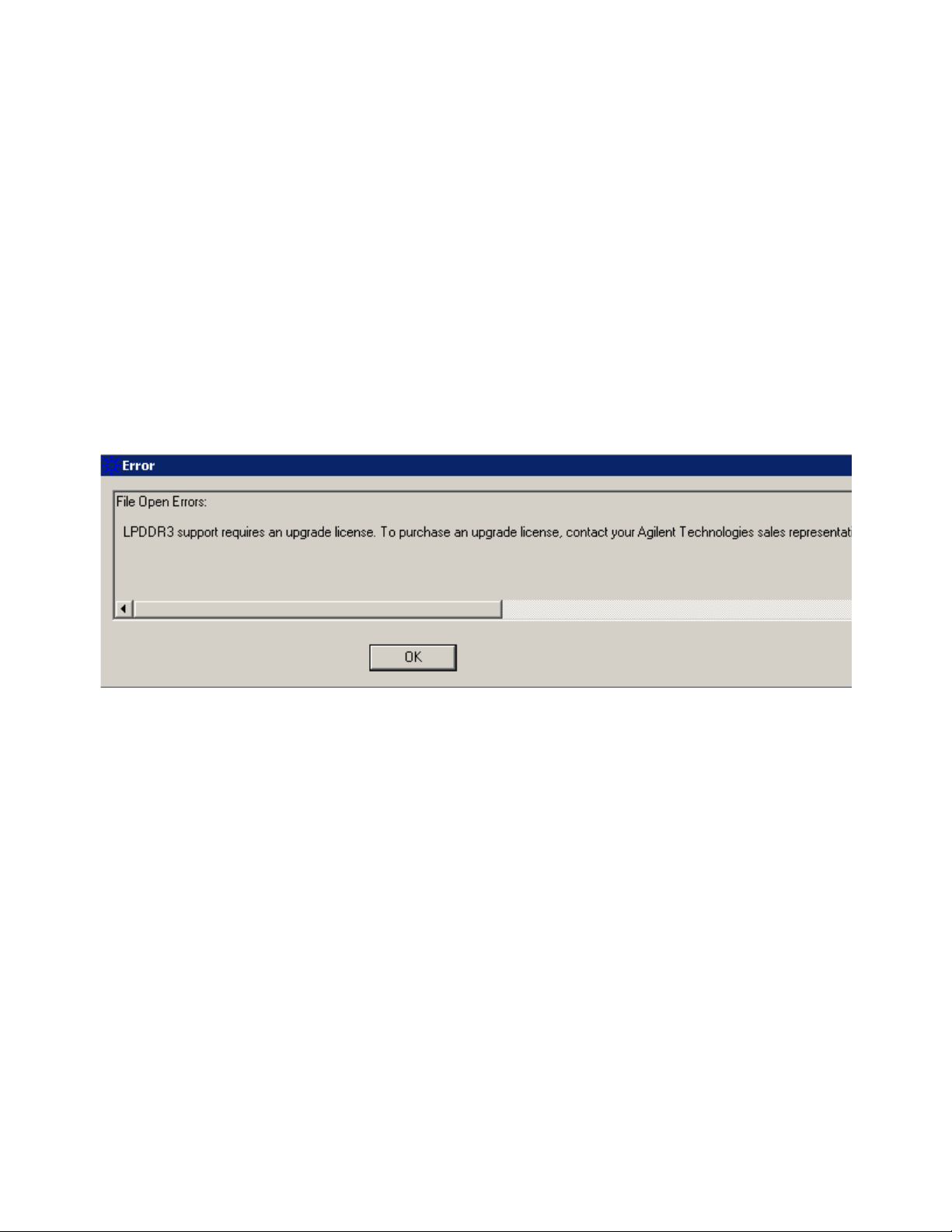
With the B4623A license, you cannot open and use an LPDDR3 configuration file.
Doing so, results in the display of the following error message.
LPDDR3 configuration files require the B4623B upgrade license. Contact Keysight
Technologies sales representative to purchase this upgrade license. Once you have
installed this license, you can access all the available LPDDR files including LPDDR3
files.
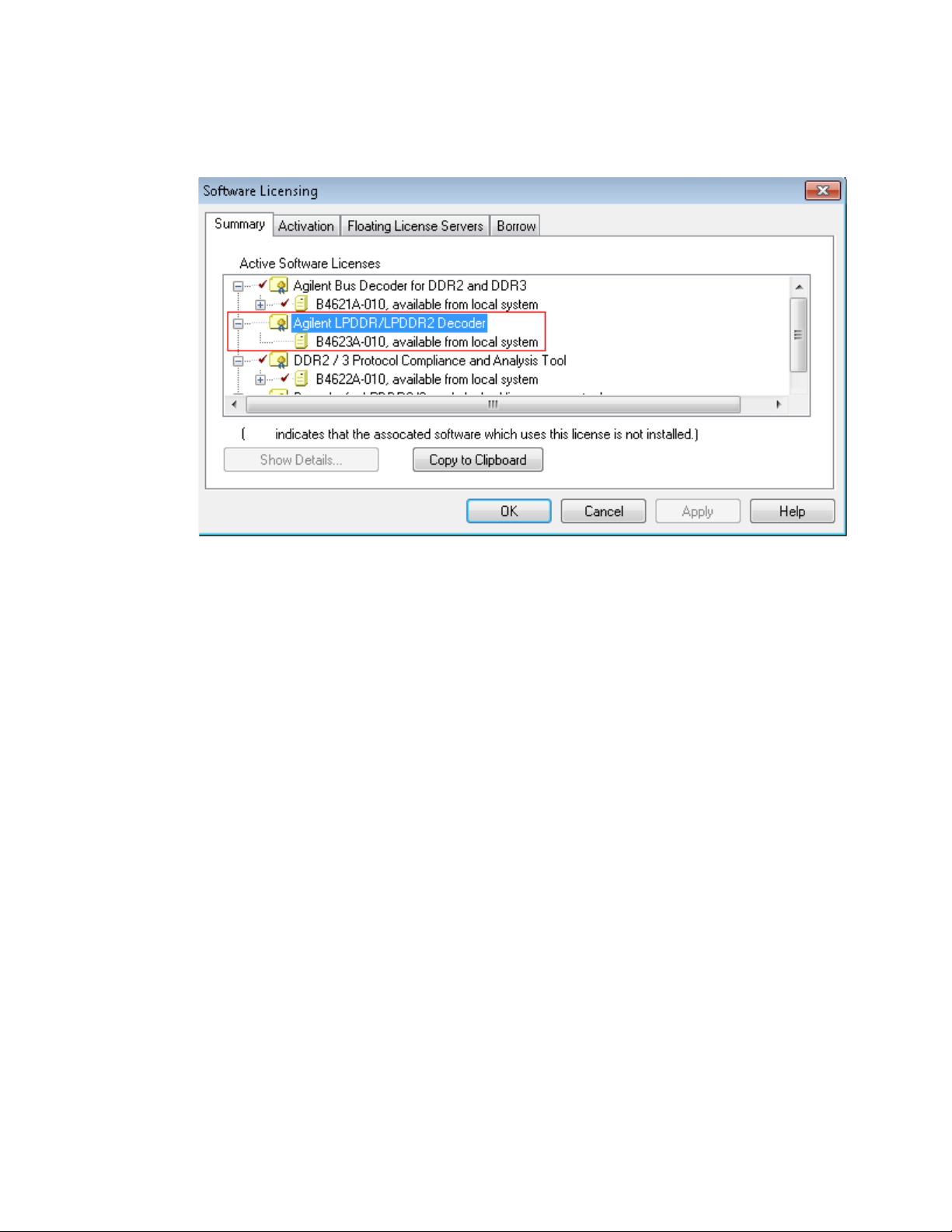
A similar error message is displayed when you have only the B4623A license and you
try to select LPDDR3 as the DDR bus type in the DDR Setup Assistant wizard while
defining the LPDDR setup.
12 B4623 LPDDR Bus Decoder User Guide
Page 13
Installing Software and Licenses 1
Upgrading to the B4623B license allows you to select LPDDR3 in the DDR Setup
Assistant wizard.
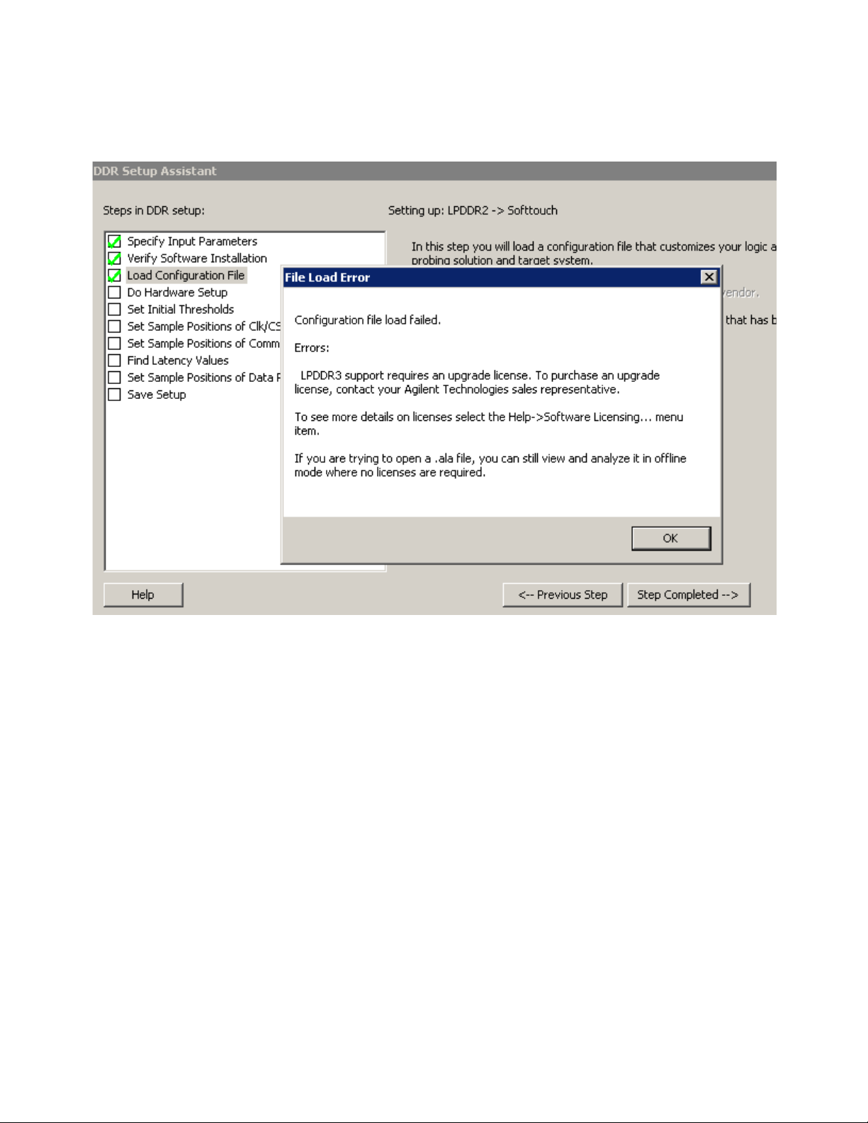
You can check if the B4623A or B4623B license is installed on your PC by clicking
Help > Software Licensing.... in the Keysight Logic and Protocol Analyzer GUI.
B4623 LPDDR Bus Decoder User Guide 13
Page 14
1 Installing Software and Licenses
See Also • "To activate software licenses" (in the online help).
14 B4623 LPDDR Bus Decoder User Guide
Page 15

B4623 LPDDR Bus Decoder
User Guide
2
Setting Up for LPDDR Bus Decode
The easiest way to set up the logic analysis system for LPDDR bus decode is by using
the DDR Setup Assistant. The DDR Setup Assistant is a wizard-like application that
helps you set up your logic analyzer properly for DDR data capture and analysis. It
guides you through the setup process and automates setting threshold voltages and
sample positions for control/address signals. See:
• "Using the DDR Setup Assistant" (in the online help)
The following topics describe how you can set up for LPDDR bus decode without using
the DDR Setup Assistant.
• “Connecting to the Device Under Test (DUT)" on page 16
• “Configuring the Decoder" on page 17
15
Page 16

2 Setting Up for LPDDR Bus Decode
Connecting to the Device Under Test (DUT)
The bus decoder is intended for use with Keysight's LPDDR memory bus probes.
You need to connect the probe to your device under test, then connect the logic analyzer
pods to the probe.
For information on how to make these connections, see the manual for the probe you are
using.
16 B4623 LPDDR Bus Decoder User Guide
Page 17

Configuring the Decoder
Configure the logic analyzer by loading a configuration file then adjusting the settings
for your device under test.
Setting Up for LPDDR Bus Decode 2
What to
Configure
Understanding
Sample
Positions and
Latency Settings
To load a configuration file
“To load a configuration file" on page 17
•
•
“To configure the decoder" on page 19
•
“To set sampling positions" on page 22
Sample Positions tell the logic analyzer when to sample each signal. If the sampling
positions are not set correctly, data cannot be captured reliably.
Total Read Latency and T otal Write Latency settings tell the decoder how to align the
captured data. These values represent the total latency for your system and therefore
should include parameters that affect total latency. If the latency settings are not correct,
data will appear to be misaligned with the corresponding command in the waveform and
listing displays.
Several Keysight provided configuration files are available for use with the LPDDR
decoder depending on the installed software license (B4623A or B4623B). With the
B4623B license, you get an additional LPDDR3 decode support that allows you to
access and use LPDDR3 configuration files as well.in addition to the LPDDR1/2 files.
When you load a configuration file, it will set up the buses and signals, add the decoder
tool, and add a listing tool.
If you are using the decoder without an Keysight LPDDR probe, see
configuration file"
To load a provided configuration file:
1 Close the logic analyzer window, if it is open.
2 Select Start>All Programs>Keysight Logic Analyzer>DDR Bus Decoder Default
Configs.
3 Select the LPDDR bus type.
4 Select the directory corresponding the model number of probe you are using and then
choose a configuration file corresponding to the bus size and speed.
When you click on a configuration file, the Logic and Protocol Analyzer software
will start and configure itself to use the decoder.
To load a provided configuration file without restarting the logic and protocol
analyzer software:
1 Select File>Open....
2 Navigate to the configuration file. The default location is:
B4623 LPDDR Bus Decoder User Guide 17
on page 18.
“To create a
Page 18
2 Setting Up for LPDDR Bus Decode
NOTE
On Windows XP
C:\Documents and Settings\All Users\Shared Documents\Keysight Technologies\
Logic Analyzer\Default Configs\Keysight\LPDDR Bus Decoder Default Configs
On Windows 7
C:\Users\Public\Documents\Keysight Technologies\Logic Analyzer\Default
Configs\Keysight\LPDDR Bus Decoder Default Configs
3 Select the file and click Open.
The provided configuration files are read-only . If you modify the configuration and want
to save your work, select File>Save As... and save the configuration with a new name.
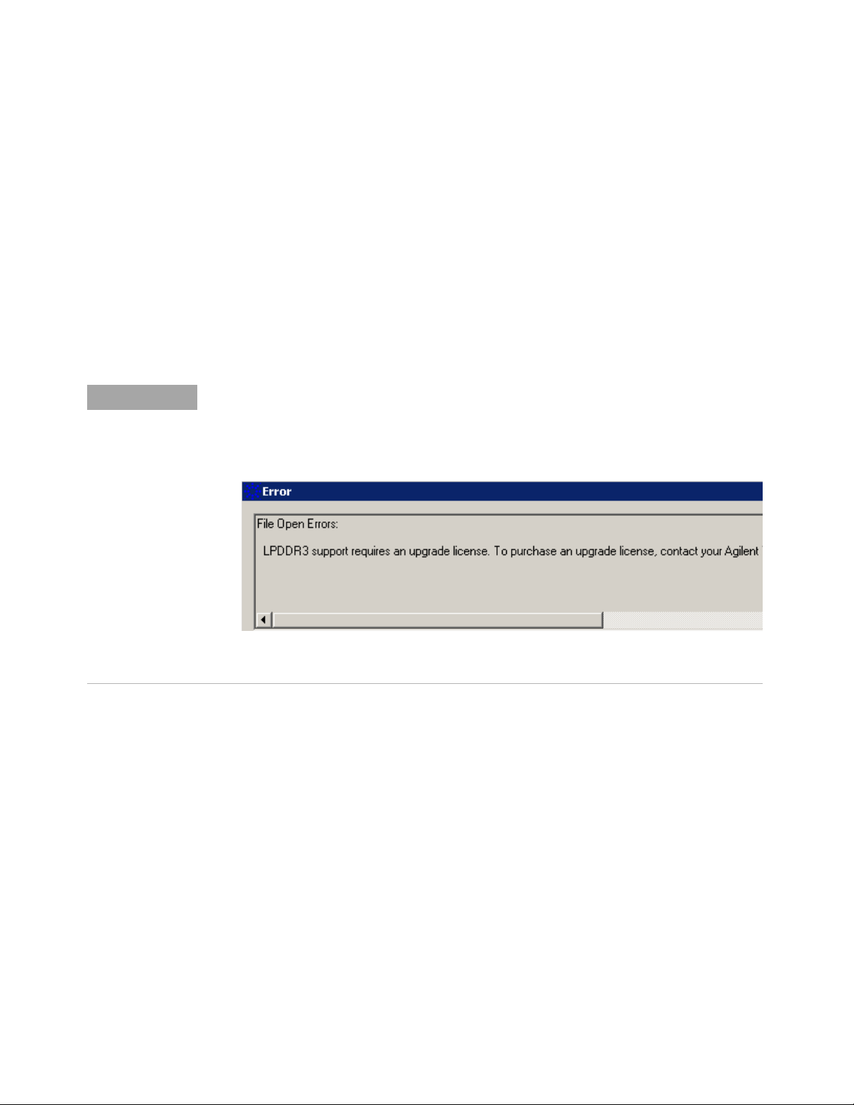
At times, when you try to open a configuration file, the following error message is
displayed. This error message indicates that the file you are trying to open requires
the upgrade license - B4623B and the license currently installed is B4623A. To open
such a file, you need to purchase and install the B4623B upgrade license.
You can verify which license of B4623 is currently installed by clicking Help >
Software Licensing in the Logic and Protocol Analyzer GUI.
See Also To update a .ala configuration file which was saved using a previous version of the
decoder, see
To create a configuration file
The provided configuration files are only valid when used with the corresponding
Keysight LPDDR memory probe.
If you are using some other probing scheme, you must create your o w n configuration
files. Extreme care must be taken to ensure that your configuration files meet the
requirements of the decoder.
• Use a provided configuration file as a model.
• Make sure that your configuration file has the same buses and signals as the provided
configuration file. The name and size of each bus and signal must be exactly the same
as it is in the provided configuration file.
“To load a configuration file from a previous version of the decoder" on page 19.
18 B4623 LPDDR Bus Decoder User Guide
Page 19

Setting Up for LPDDR Bus Decode 2
• Verify that the buses and signals listed in “Buses and Signals Captured by the Logic
Analyzer"
To simplify the procedure of customized configuration file creation, Keysight provides
the DDR/LPDDR Custom Configuration Creator tool. The tool ensures that all the
layout information needed by LPDDR Decoder is included in the created configuration
file.
This tool is a part of the Keysight DDR Setup Assistant and Eyefinder software package.
Therefore, the tool is available only after you install this package.
To know more about this tool, refer to its online help that gets installed with this tool’s
software.
on page 46 are all present.
To load a configuration file from a previous version of the decoder
When you upgrade the decoder, the new v ersion of the d ecoder may have dif feren t input
buses and signals. If you load an .ala configuration file which was saved with the old
version of the decoder, you may see error messages. Follow this procedure to update the
configuration file for the new decoder.
1 Open the .ala configuration file.
2 Write down the user preferences or take a screen shot of the user preferences.
3 Save the configuration file (with data) using the .xml format.
4 Open the Overview display and remove the decoder.
5 Load the .xml configuration file.
6 Add the decoder.
7 Restore the user preferences.
8 Save the configuration as using the .ala format.
To configure the decoder
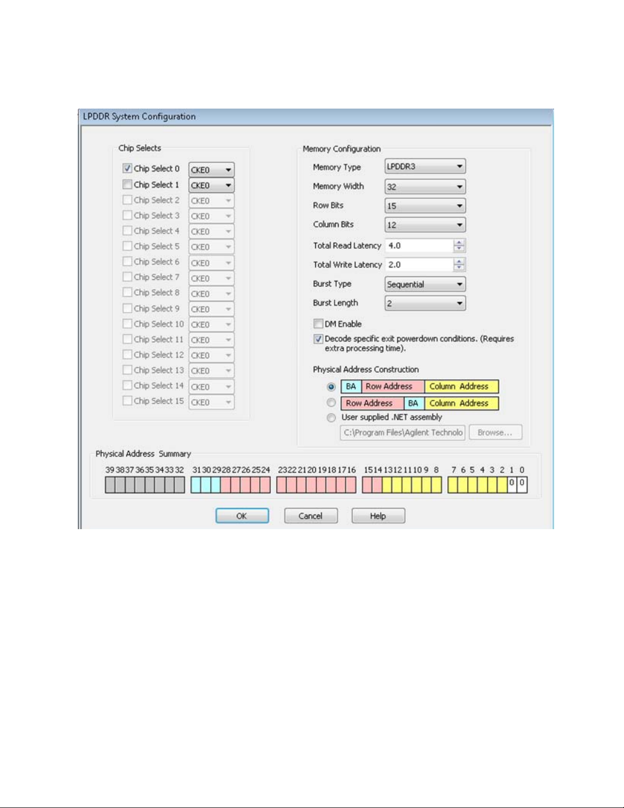
Use the System Configuration dialog to tell the decoder which chip selects will be used
by your device under test and to specify details about how the bus works.
To open the
System
Configuration
dialog
• From the main menu bar, select Tools>DDR Bus Decoder>System Configuration,
or
• In the Overview display, click the Properties button on the LPDDR Bus Decoder
tool then select System Configuration.
B4623 LPDDR Bus Decoder User Guide 19
Page 20
2 Setting Up for LPDDR Bus Decode
Chip Selects All of the chip selects that are being used in the system must be enabled; otherwise, the
decoder will not function correctly. Likewise, any chip selects that are not used must not
be enabled.
You must tell the decoder about the chip selects because chip selects are active low and
unconnected logic analyzer channels float low. Without the enables, the decoder could
not tell the difference between active and unconnected chip selects.
The decoder compares the chip selects which are enabled in this dialog with the CS# bits
for each state captured by the logic analyzer. It will decode only those states where the
chosen chip selects are active (low).
There can be 1 to 16 chip selects, depending on the size of the CS# bus. If the size of the
CS# bus indicates that fewer than 16 chip selects are being used, the unused chip selects
are disabled in the dialog.
20 B4623 LPDDR Bus Decoder User Guide
Page 21

Setting Up for LPDDR Bus Decode 2
For each of the enabled chip selects, choose which clock enable signal is used. A state
will only be decoded when both an enabled chip select and the corresponding clock
enable bit are active. The choices are determined by the number of bits in the CKE bus.
If only CKE[0] is present, you do not need to make a selection.
Memory Type Choose the type of memory you are using.
Memory Width This value is used to compute physical addresses. For memory widths greater than 8 bits,
the column address is padded with the appropriate number of 0 bits. You can see how
this works by examining the Address Summary at the bottom of the dialog as you select
different memory widths.
Row Bits and
Column Bits
Total Read
Latency and
Total Write
Latency
Burst Type Select the order of the bytes after the Read/Write Command (Sequential or Interleaved).
Choose the number of Row Bits from the ROWADDR bus that are valid during the
Activate cycle. The number of Row Bits will match the number of pink bits in the
Address Summary at the bottom of the dialog.
Choose the number of Column Bits from the COLADDR bus that are valid during the
Read or Write cycle. The number of Column Bits will match the number of yellow bits
in the Address Summary at the bottom of the dialog.
If ROWADDR and COLADDR are properly defined to reflect the number of bits in your
device under test, when the LPDDR Decoder tool is added to the logic analyzer, the Row
Bits and Column Bits will automatically be set to the proper values.
If using LPDDR2, then COLADDR[0] must also be defined. Assign COLADDR[0] to
any unused channel, and set the signal threshold so that COLADDR[0] is always zero.
Enter the number of full clock cycles between the time that a read or write command
appears on the bus and the time when valid data appears on the data bus. These values
represent the total latency for your system and therefore should include parameters that
affect total latency.
These latency settings are affected by several factors, including the inherent read latency
of the memory part, the posted additive latency, write leveling, and the logic analyzer
sample position.
The decoder uses this setting to calculate and display the appropriate physical address
for each memory cycle.
Burst Length Select the number of bursts after a Read/Write Command.
DM Enable Enables write data masking. This option is available only when the DM_W bus exists. If
DM Enable is set, the decoder will apply the DM_W bits to the DATA_W bits before
displaying the write data value in the 'DDR Bus Decode' column.
For example, if:
DM = enabled
Memory Width = 32
DM_W = 0001
DATA_W = 0123 4567
then the decoder will display the data as:
B4623 LPDDR Bus Decoder User Guide 21
Page 22

2 Setting Up for LPDDR Bus Decode
mem write 0x 0123 45--
This option is disabled if the DM_W bus does not exist.
Decode specific
exit powerdown
conditions
Construction
Summary
Choose whether or not you want the LPDDR Decoder to decode and display the specific
power down events from which the DUT exited.
If you deselect this checkbox, the decoder records power down entries and exits but does
not decode the specific event in case of exits. Instead, it displays a generic exit label in
the Listing window for all such exit events.
For detailed information on how to decode and view self refresh and power down events,
refer to the topic
Physical
Address
Address
See Also • To find the Row and Column Bits and Burst Length, refer to the technical data sheet
Choose whether the physical (linear) addresses should be constructed from
{BA,RA,CA} or {RA,BA,CA}. In most cases, the physical address is constructed from
{BA,RA,CA}.
If your system uses a different convention, you need to create a .NET assembly to
translate between a physical address and the various fields which make up a bus address.
If this is the case, select "User supplied .NET assembly" and refer to
“Customizing Physical Address Construction,” starting on page 63.
The address summary is a picture that shows how physical addresses will be constructed,
based on user inputs for Memory Width, Row Bits, Column Bits, and Bank Address
Location.
for the DDR memory part you are using or capture data from a mode register set
(MRS) cycle as the device under test boots up.
“Decoding Self Refresh and Power Down Events" on page 35.
Appendix A,
To set sampling positions
Data on the LPDDR bus is valid for a very short time. Sample positions tell the logic
analyzer when each signal is valid. You must adjust the logic analyzer's sample positions
in order to reliably capture data on your bus. In addition, you must set the Total Read
Latency and T otal W rite Latency in the decoder so that data in the listing will be properly
aligned.
The Keysight logic analyzer requires a single clock for all data acquisition. All signals
are sampled on both edges of the sample clock. You need to identify correct sample
points for three clock groups: Command and Address, Read Data, and Write Data.
1 Install the memory bus probe and connect it to the logic analyzer.
2 Load the default configuration into the logic analyzer.
3 Configure the memory bus.
4 Power up the target with a stimulus that exercises the range of available memory.
5 Set the sampling positions for the Command and Address signals
(LPDDR2/LPDDR3 (see
22 B4623 LPDDR Bus Decoder User Guide
page 23), LPDDR1 (see page 23)).
Page 23
Setting Up for LPDDR Bus Decode 2
6 Set the logic analyzer sampling positions for Read Data and Write Data. There are
two ways to do this:
• Set sampling positions with the DDR3 Eyefinder (see
procedure to set sample positions using an automated tool.
• Set sampling positions manually (see
You can also use this procedure for LPDDR2/LPDDR3 if you have full control of
the bus (so you can to generate separate read and write traffic) and you want
precise control over sample positions.
7 Set the Total Read Latency and Total Write Latency in the decoder.
page 27) — Use this procedure for LPDDR.
page 27) — Use this
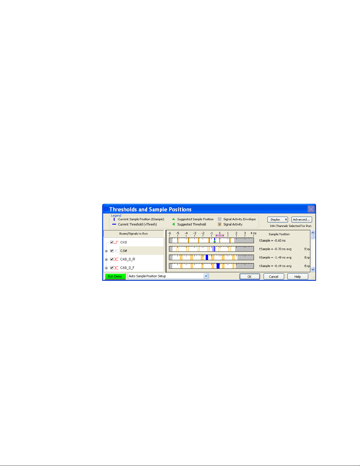
To set sampling positions for LPDDR2/LPDDR3 Command and Address
1 Set CK0 in the first eye just to the left of 0.
2 Set CS# and CKE in the similar eye (just left of 0).
3 Then set CA9_0_R one eye to the left and set CA9_0_F in the eye that is most similar
to CS#. Refer to the diagram below.
Setting the signals CA9_0_R and CA9_0_F automatically adjusts all of the other
Command and Address buses/signals. (There is no need to adjust ST AT , ROWADDR,
COLADDR, COMMAND, COMMAND0, BA, AB, AP or any other command or
address bus signal.)
To set sampling positions for LPDDR1 Command and Address
The Command and Address group of signals consists of CK, CKE, COMMAND,
ADDR, BA, CS#, ODT and RESET#.
The supplied configuration files set the logic analyzer to sample on the rising and falling
edge of the clock, with no positive or negative delay. You should fine-tune the sampling
position for your measurement setup.
Capture some
data
B4623 LPDDR Bus Decoder User Guide 23
1 Configure the decoder (see page 19).
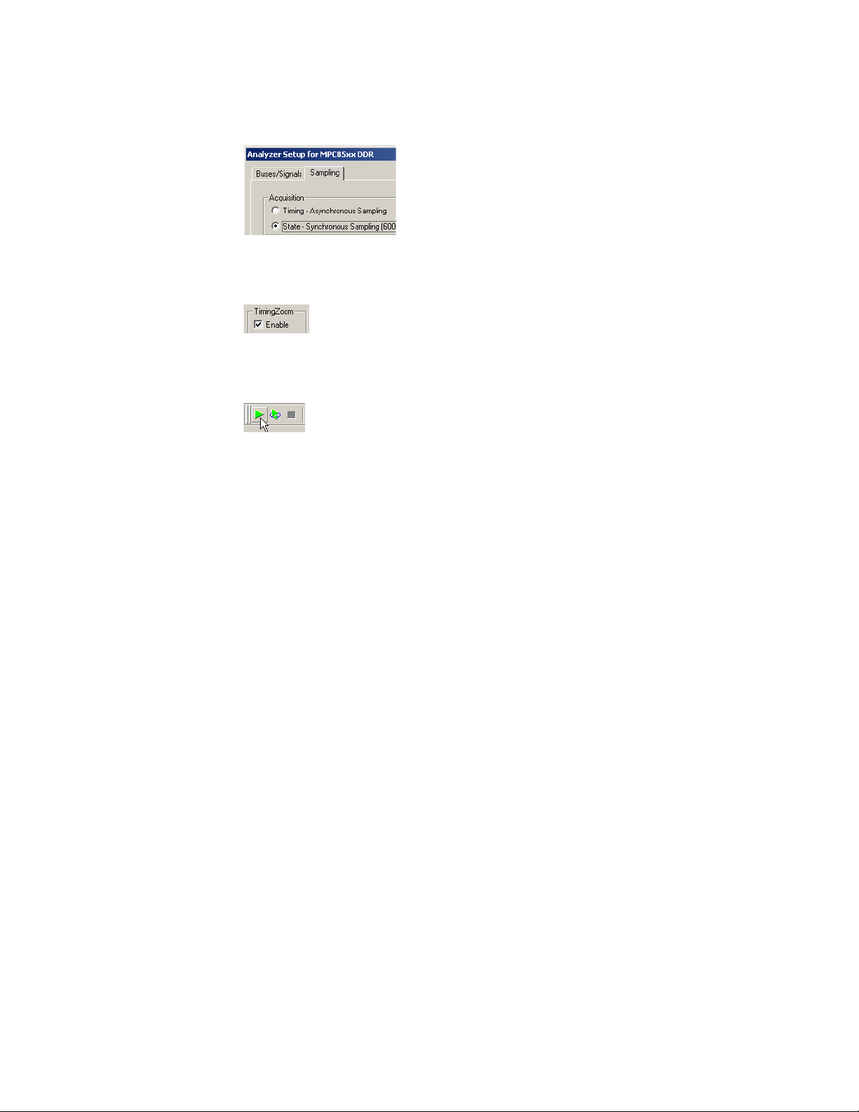
2 Go to the Sampling tab.
Page 24
2 Setting Up for LPDDR Bus Decode
3 Check that TimingZoom mode is enabled (on some analyzers).
4 Capture some data. To do this, run the analyzer then stop it manually.
Set the sampling
positions
Verify the
sample positions
1 Open the Sampling tab of the Analyzer Setup dialog.
2 Select Thresholds and Sample Positions....
3 Select the signals associated with the address group.
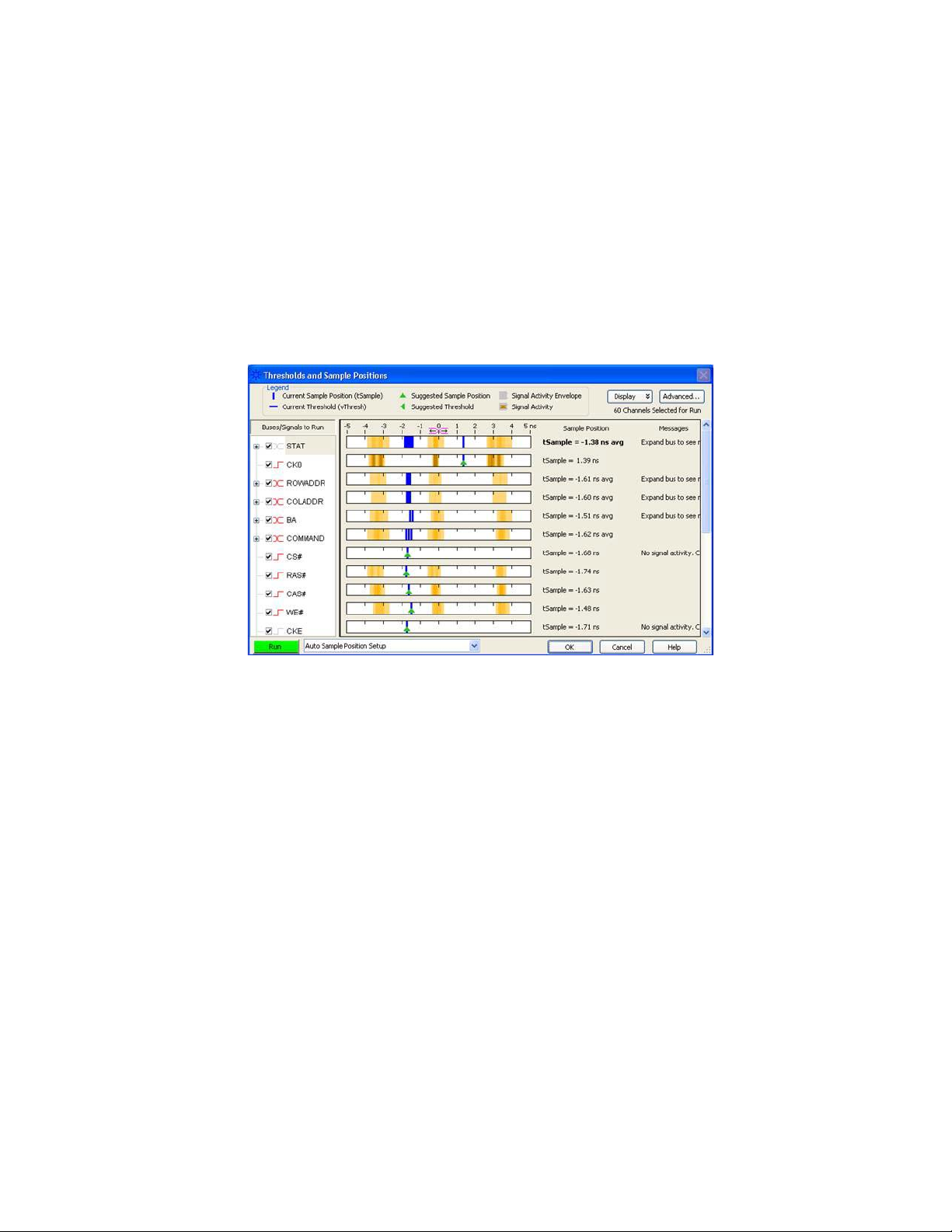
4 At the bottom of the dialog, select Run the Auto Sample Position Setup and click
Run.
At this point, the results should approximate the initial sample positions from the
configuration.
Some signals may not be active. CKE[1] is only active in dual and quad rank
configurations. Some of the upper ADDR signals may not be active depending upon the
size of the memory size in the target. ODT[1] will not be active in all target
configurations.
Note that using Eye Scan with Sample Position Setup Only can often provide a better
picture of the active and inactive signals.
1 Run the logic analyzer to capture some data with the new sample positions.
2 In the Waveform window, find a valid DDR command cycle (for example, when
CAS=0). The RAS, CAS, WE, and ADDR signals should all be valid on the rising
edge of the clock (CK). If necessary, adjust the sample position for each of these
signals so that the data eye is centered on the rising edge of the clock,
3 Capture some more data to ensure that the command signals are centered.
See also
24 B4623 LPDDR Bus Decoder User Guide
“Example: Sampling Positions for Command and Address" on page 25.
Page 25
Setting Up for LPDDR Bus Decode 2
Set the sampling
position for the
clock
Example:
Sampling
Positions for
Command and
Address
Example:
Typical sample
positions
1 Set the sampling position for CK so that it is centered 1/4 clock period after the rising
edge of CK. In other words, CK must sample itself midway between the rising and
falling edges.
B4623 LPDDR Bus Decoder User Guide 25
Page 26
2 Setting Up for LPDDR Bus Decode
Example:
Waveform
display
Example:
Manually
adjusting
sample positions
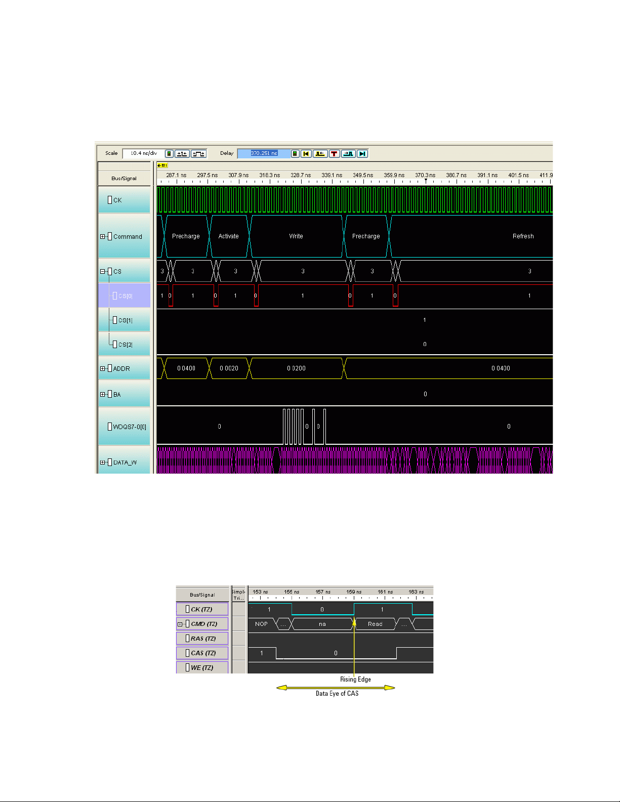
1 Run the logic analyzer to capture some data with the new sample positions.
2 In the Waveform window, find a valid DDR command cycle (for example, when
CAS=0). The RAS, CAS, WE, and ADDR signals should all be valid on the rising
edge of the clock (CK). If necessary, adjust the sample position for each of these
signals so that the data eye is centered on the rising edge of the clock,
26 B4623 LPDDR Bus Decoder User Guide
Page 27

Setting Up for LPDDR Bus Decode 2
NOTE
To do this:
a For each signal, note how far it needs to move to be centered under the rising
clock edge.
In the picture above, the center of CAS signal is about 1.3 ns before the rising
edge of the clock. Note that since the other command signals are held high, you
would need to find a dif ferent comm and cycle to see how the e yes of thos e signals
line up with the clock.
b Open the Sampling tab of the analyzer Setup dialog.
c Select Thresholds and Sample Positions....
d Change the sample positions.
3 Capture some more data to ensure that the command signals are centered.
To set sampling positions using DDR3 Eyefinder
The DDR3 Eyefinder is an extension of Keysight's eye finder and eye scan technology . It
helps select sample positions for the data signals on the LPDDR2 bus.
The DDR3 Eyefinder application can be used to identify the correct sample position on
the data bus. This tool is designed to work even when the target is not able to generate
selective read-only or write-only activity on the memory bus. The application is able
selectively examine only the active data portion of read cycles or write cycles on a bus
with mixed traffic.
The Command and Address sample positions must be properly selected before utilizing
this tool.
See • "Your First DDR3 Eyefinder Scan" (in the online help)
To set sampling positions manually
If you have the ability to produce read-only and write-only data on the bus of your
device under test (using ITP control or equivalent), you can generate patterns on the bus
and set the sampling positions manually.
Data is valid on rising/falling edge of the associated data strobe signals, but the logic
analyzer does not have the ability to latch data using the separate data strobes. Instead,
the analyzer latches data based on the comma nd clock (CK). The data strobes and CK
are not necessarily in phase, thus the sample position for individual data signals must be
adjusted relative to CK.
B4623 LPDDR Bus Decoder User Guide 27
Page 28

2 Setting Up for LPDDR Bus Decode
Keep in mind that read eyes and write eyes occur on the same signals, but at different
times. A mix of read-data and write-data data will confuse eye finder because it will not
be able to converge on a single eye. T o use eye finder to refine the data sample positions,
bus activity on the data bus must be limited to just reads or just writes.
Setting sample
positions for
Read Data
Once the Command and Address sample positions have been set, The next task is to
identify the correct sample positions for the Read Data. The read data is synchronous to
the DQS strobes. In a stable system there is a fixed phase offset between the common
clock and the strobes. In addition, there is a fixed clock delay between the read
commands and the start of each data transfer. The clock del ay is entered into the decoder
setup. The phase offset requires use of the Threshold and Sample Position tool using the
Auto Eye Scan with Sample Position Setup Only application.
1 Set up your device under test to generate known, continuous read-only data patterns
on the memory bus. A pattern that works well is alternating 0xFFFFFFFF and
0x00000000.
2 On the logic analyzer Threshold and Sample Positions menu deselect the Command
and Address Group signals and select DATA_R, CB_R and DQS_R.
3 Run the Auto Eye Scan with Sample Position Setup Only application. The data bus is
not actively driven between data transfers.
In many systems the signals float around the threshold. This signal level uncertainty
between data transfers prevents the Threshold and Sample Positions tool from
automatically selecting the correct sample position. The picture below provides an
example of the results of an Eye Scan with Sample Position Setup Only and how to
interpret the results to obtain the correct sample position.
28 B4623 LPDDR Bus Decoder User Guide
Page 29

Setting Up for LPDDR Bus Decode 2
B4623 LPDDR Bus Decoder User Guide 29
Page 30

2 Setting Up for LPDDR Bus Decode
4 Once the read data sample positions are selected, find the correct sample for the
DQS_R signal. Utilize the waveform view of the state acquisition.
Setting Sample
Positions for
Write Data
The final group is the Write Data.
1 Set up your device under test to generate known, continuous write-o nly data p att ern s
on the memory bus. A pattern that works well is alternating 0xFFFFFFFF and
0x00000000.
2 In the Threshold and Sample Positions tool deselect the read data group and select the
DATA_W, DM_W, CB_W and DQS_W labels.
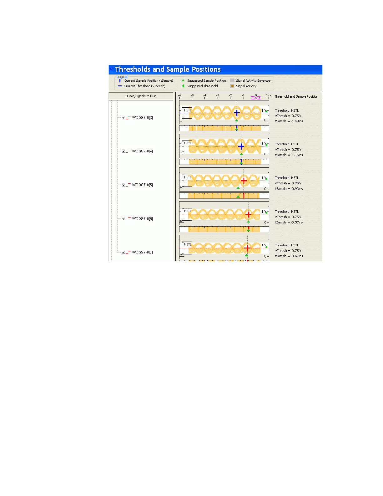
3 Run the sample position application as with the read data bus and set the sample
position for each bit.
Some system do not utilize the Check Bit (ECC) signals or all of the Data Mask
(DM) signals.
The picture below shows an example of the sample positions for Write Data:
30 B4623 LPDDR Bus Decoder User Guide
Page 31
Setting Up for LPDDR Bus Decode 2
B4623 LPDDR Bus Decoder User Guide 31
Page 32
2 Setting Up for LPDDR Bus Decode
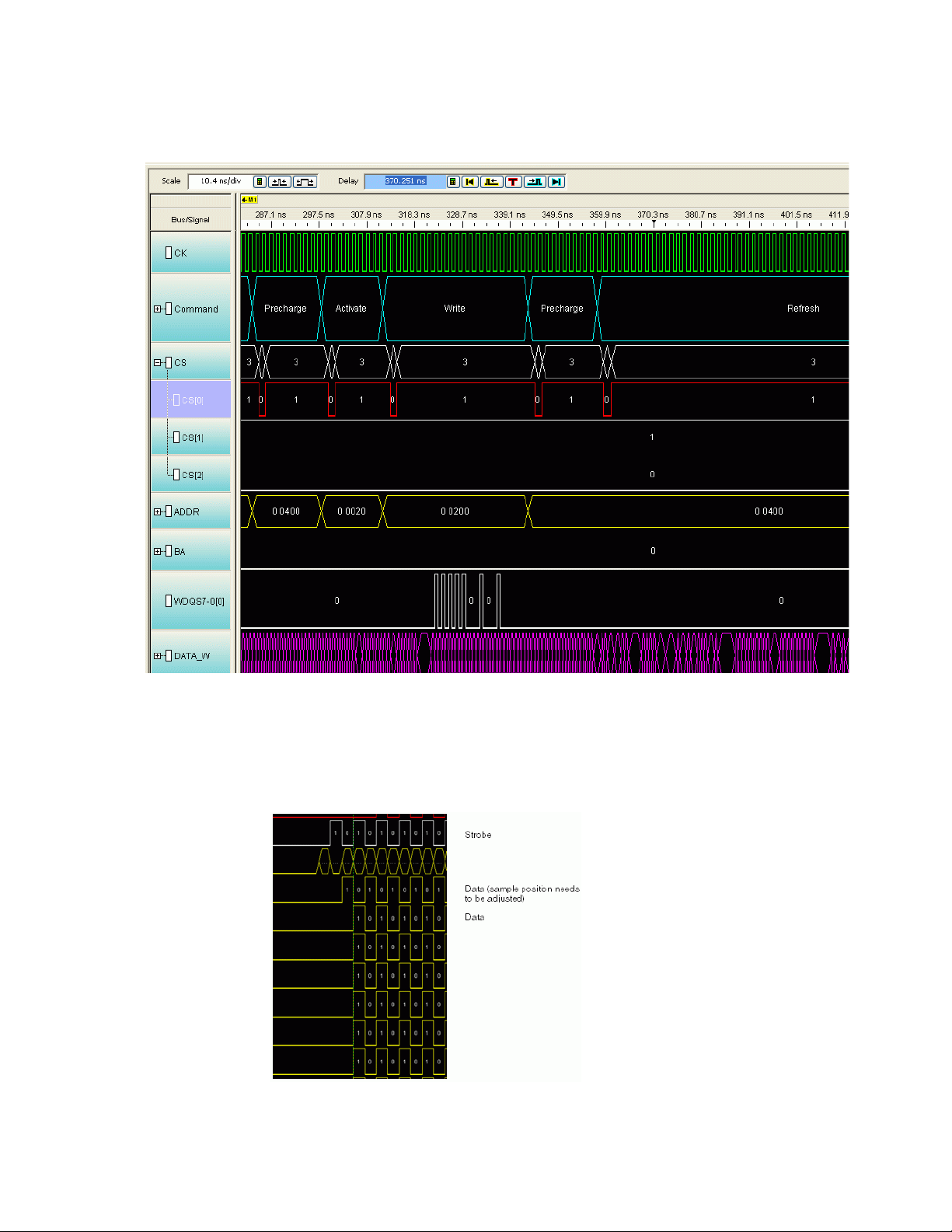
4 To check that all of the Write Data bits are aligned, configure the target to generate
write-only traffic with an alternating 0/1 bit pattern. If necessary, select a different
eye opening so that each DQ signal is sampled at the same time. In the following
example, the first data bit needs to be adjusted:
32 B4623 LPDDR Bus Decoder User Guide
Page 33

Setting Up for LPDDR Bus Decode 2
You do not need to rerun Eye Scan, but you run the logic analyzer after each
adjustment to verify the results.
5 When you are done, check the Listing display to verify that the bit patterns have been
captured correctly.
Tips for setting
sample positions
Generating Data
for Auto Sample
Position and
Auto Threshold
Setting the
Threshold
Remember that the waveform display on the logic analysis system is a state waveform
(timing is aligned to each sample), not the timing waveform you would see if the logic
analyzer was running in Timing mode.
The threshold settings for signals can have a significant effect on the ability of the logic
analyzer to accurately sample the signals. Targets with asymmetric signal swings or
using a voltage different from the 1.5 Volt standard may need additional modification to
the standard logic analyzer configuration. If you are unable to find sample positions that
support accurate sampling of the signals on the LPDDR2 bus, use the Auto Threshold
and Sample Position Setup application in the Threshold and Sample Positions tool.
Because of the float time on the data bus between transfers, do not depend upon the
thresholds or positions selected by this tool. Manually view each eye diagram and
modify the threshold and position to best select the center of the active portion of each
eye.
In order to run Auto Sample Position Setup and Auto Threshold on the Data signals it is
important that the device under test is programmed to generate exclusively Write or
Read traffic of a known pattern, such as F's and 0's. This is the only way to get usable
data windows to set the sampling positions of both the Read and Write Data labels on the
logic analyzer. At these speeds even one half a data strobe bit width of timing
relationship shift between the strobe (clock) and the data bits will eliminate the window.
The Threshold setting for clocks and signals can have a significant effect on the size of
the eyes. At speeds of 800 MT/s or higher even a 50 mV change in the threshold can
make all the difference in the eye size as measured at the logic analyzer. The best way to
determine this level is through trial and error, or through use of the Auto Threshold
function.
B4623 LPDDR Bus Decoder User Guide 33
Page 34

2 Setting Up for LPDDR Bus Decode
34 B4623 LPDDR Bus Decoder User Guide
Page 35

B4623 LPDDR Bus Decoder
User Guide
3
Decoding Self Refresh and Power
Down Events
The LPDDR Decoder supports decoding and displaying the entry to and exit from Self
Refresh and Power Down events. Once data is captured and decoded, you can view the
entry and exit from the following events in the Listing window of the Logic and Protocol
Analyzer GUI.
• Power down
• Deep power down
• Self refresh
To ensure that entry and exit from these events are decoded and displayed in the Listing
view, you need to complete the following steps before capturing data.
• Disable clock qualifiers
• Set the clock threshold
35
Page 36
3 Decoding Self Refresh and Power Down Events
Disabling Clock Qualifiers
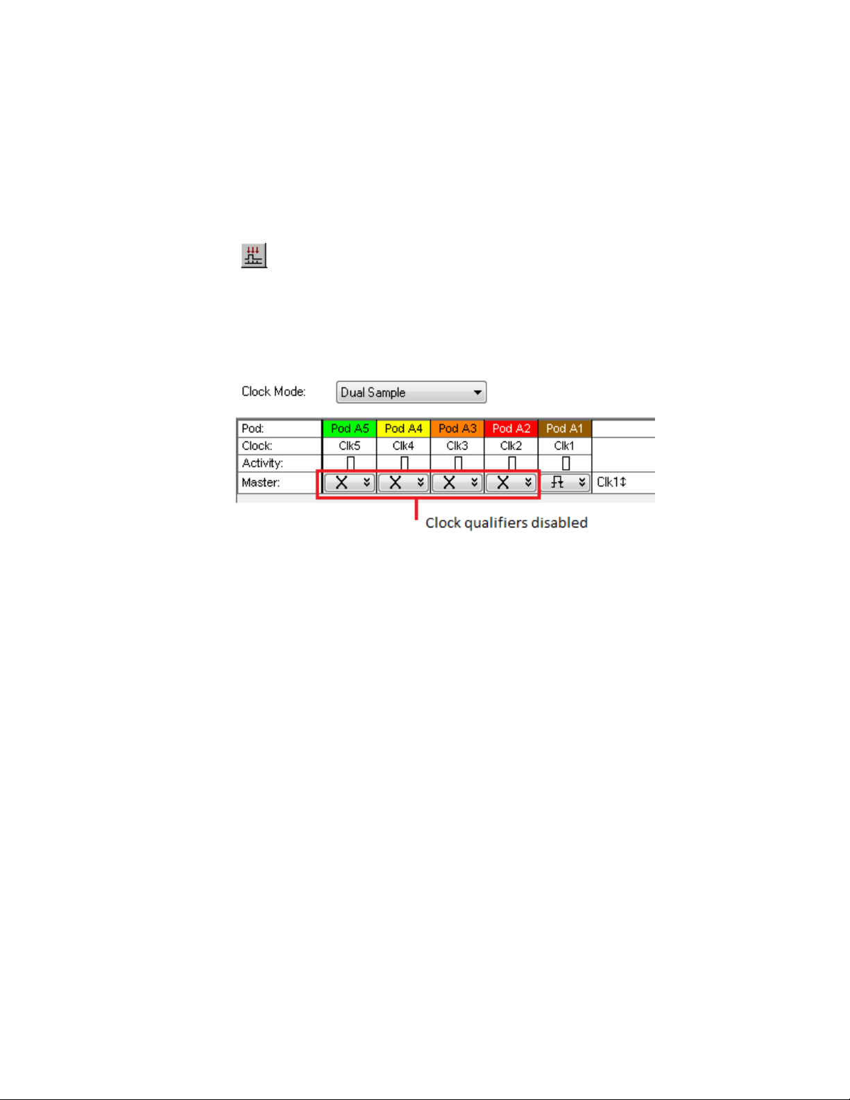
The LPDDR Decoder will not be able to decode and display power down and self refresh
events if the clock qualifiers are enabled.
1 Access the Sampling tab of the Analyzer Setup dialog box by clicking the
toolbar button in the Logic and Protocol Analyzer GUI. Ensure that you have
loaded the LPDDR configuration file/setup in the Logic and Protocol Analyzer GUI
before this step.
2 In the State Options group box, select Don’t Care for all the clock qualifiers to
disable these qualifiers.
3 Click OK.
36 B4623 LPDDR Bus Decoder User Guide
Page 37
Setting the Clock Threshold
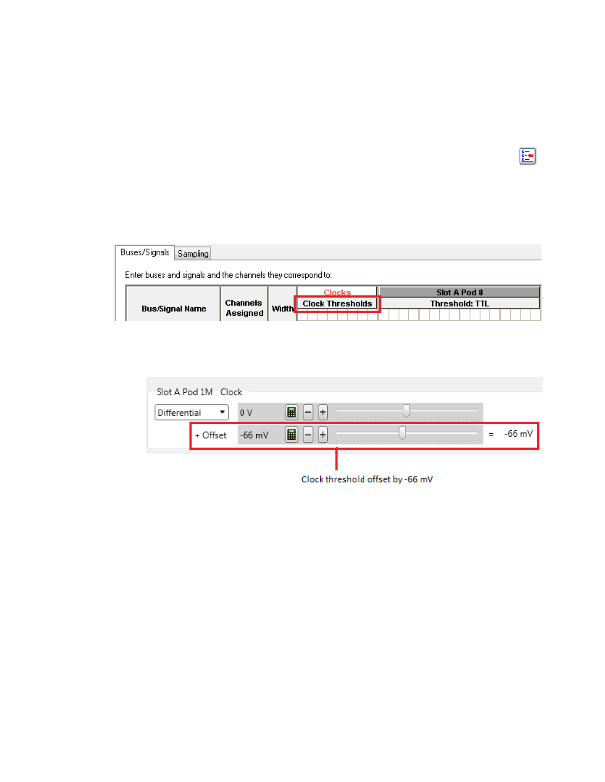
The clock threshold should be offset by a negat ive amount in the ran ge of -60 to -70 mV.
1 Access the Buses/Signals tab of the Analyzer Setup dialog box by clicking the
toolbar button in the Logic and Protocol Analyzer GUI. Ensure that you have loaded
the LPDDR configuration file/setup in the Logic and Protocol Analyzer GUI before
this step.
2 Click the Clock Thresholds button displayed under the clock label.
3 In the Threshold Settings for Clock Channels dialog box, set the offset of the clock
within the range -60 to -70 mV.
Decoding Self Refresh and Power Down Events 3
4 Click Done.
B4623 LPDDR Bus Decoder User Guide 37
Page 38
3 Decoding Self Refresh and Power Down Events
Viewing Power Down Events
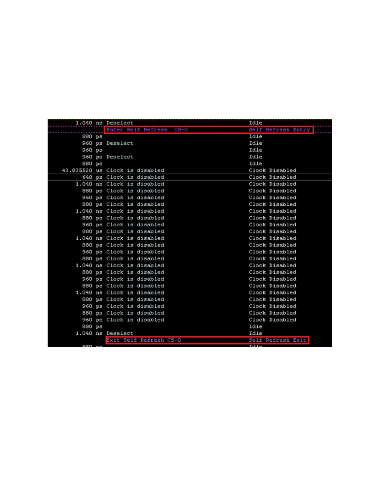
Once the above-mentioned steps are performed, the self refresh and power down events
are decoded and displayed. The following screen displays an example of an entry to and
exit from the self refresh event in the Listing window.
38 B4623 LPDDR Bus Decoder User Guide
Page 39

Decoding Self Refresh and Power Down Events 3
Enabling/Disabling Decode and Display of Specific Power Down Exit Events
By default, the LPDDR Decoder decodes and records the specific power down event
from which the DUT exited. This, however, requires extra processing time for
ascertaining the specific exit event on the basis of the last entry event. If you want to
reduce this processing time and do not want to view the specific power down event from
which the DUT exited, then you can disable this feature.
When you disable this feature, the decoder records these power down entries and exits
but does not decode the specific event in case of exits. Instead, it displays a generic exit
label in the Listing for all such exit events.
The following screen displays a Listing of such events when this specific exit event
decoding feature is disabled. Notice that the exit is labeled as a generic exit from self
refresh or power down conditions instead of a specific event from which the exit was
made.
B4623 LPDDR Bus Decoder User Guide 39
Page 40
3 Decoding Self Refresh and Power Down Events
To enable/disable the display of specific exit events
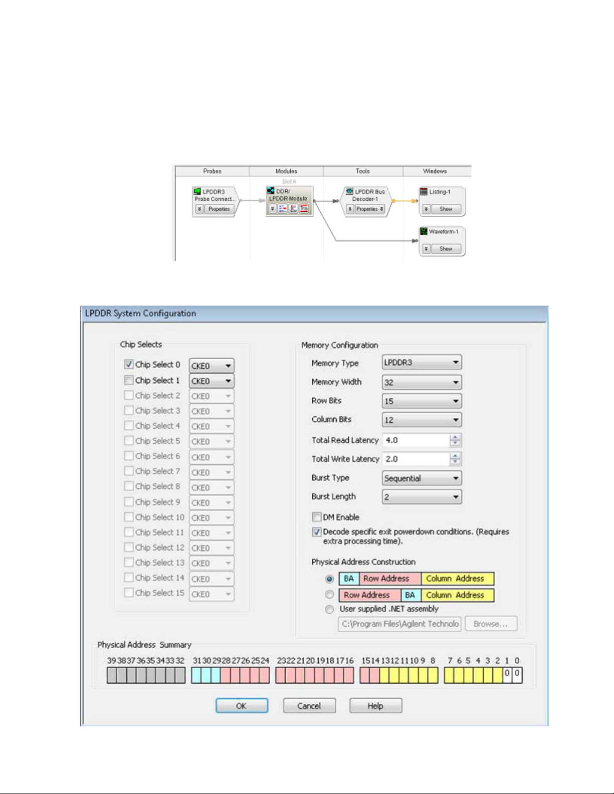
1 In the Overview display, click the Properties button on the LPDDR Bus Decoder
tool then select System Configuration.
The LPDDR System Configuration dialog box is displayed.
40 B4623 LPDDR Bus Decoder User Guide
Page 41

Decoding Self Refresh and Power Down Events 3
2 By default, the feature to decode specific exit power down events is enabled. To
disable it, deselect the Decode specific power down conditions checkbox.
3 Click OK.
B4623 LPDDR Bus Decoder User Guide 41
Page 42

3 Decoding Self Refresh and Power Down Events
42 B4623 LPDDR Bus Decoder User Guide
Page 43

B4623 LPDDR Bus Decoder
User Guide
4
Capturing Data
To capture any data, the logic analyzer must run a measurement then end the
measurement (either manually or by detecting a trigger).
To trigger on an
address
Normally, the trigger will be an address detected on the bus.
1 Set the logic analyzer to trigger when the address is encountered. You may need to
convert (see
appear on the bus.
2 "Run" (in the online help) the logic analyzer.
3 Run the device under test.
The logic analyzer will trigger when address is found on the bus.
page 44) a physical address to the row and column addresses which will
43
Page 44

4 Capturing Data
To convert to and from physical addresses
Use the Address Conversion Tool dialog to convert a physical (linear) address into an
equivalent bank address. You can also use the tool to convert a bank/row/column address
into a physical address. Before you use this tool, you must configure the decoder (see
page 19).
The dialog contains three representations of the address:
• Bus Address
• Physical Address (hexadecimal)
• Physical Address (graphical summary showing each bit)
You can edit any of these representations. As you make changes, the other
representations are calculated and displayed immediately.
To open the
Address
Conversion Tool
To convert a
row/column
address to a
physical address
To convert a
physical address
to a row/column
Address
Summary
dialog
address
• From the main menu bar, select Tools>DDR Bus Decoder>Address Conversion
Tool, or
• In the Overview display, click the button on the DDR Bus Decoder tool and select
Address Conversion Tool.
Enter the row address, column address, and bank address. These values will be
constrained by the memory bus options you set in the System Configuration dialog. The
physical address will be updated continuously to reflect the values you enter.
Enter the physical address. The other values will be updated continuously as you enter
the address.
The address summary is a picture that shows how the physical address is constructed,
based on user inputs for Memory Width, Row Bits, Column Bits, and Bank Address.
44 B4623 LPDDR Bus Decoder User Guide
Page 45

B4623 LPDDR Bus Decoder
User Guide
5
Understanding the Listing
The DDR data bus is displayed as raw hexadecimal data. The deco der does not inverse
assemble the data payload.
Columns in the
listing
For an explanation of the columns in the listing, see:
• “Buses and Signals Captured by the Logic Analyzer" on page 46
• “Buses Generated by the Decoder" on page 52
45
Page 46

5 Understanding the Listing
Buses and Signals Captured by the Logic Analyzer
Required input
buses
The following buses must be present in the input data to connect with the Keysight
LPDDR/LPDDR2/LPDDR3 Decoder, DDR2/3 EyeFinder and DDR2/3 External
Applications. They are automatically provided by the default configuration files. If you
create your own configuration file (see
page 18), be sure to define all of the required
buses.
Bus Name Description
ADDR Address signals. 14 bits wide. (LPDDR1 only)
ROWADDR Address signals used during an activate command. Typically these are
called the Row Address signals. ROWADDR is typically used by the
LPDDR decoder and by the DDR Trigger application. It is also used by a
variety of tools to read the size of the ROW ADDR to determine the number
of Row bits valid during an active.
COLADDR Address signals used during a read/write command. Typically these are
called the Column Address signals. COLADDR is typically used by the
LPDDR decoder and by the DDR Trigger application. It is also used by a
variety of tools to read the size of the COLADDR to determine the number
of Column bits valid during a read or write.
CK0 Clock signal used by LPDDR/LPDDR2/LPDDR3. This is the signal that
was used to clock the analyzer. This signal must be a single bit.
CKE Clock enable bits. 1 or more bits wide (depending on how many clock
enable signals are used by your memory system). The decoder will decode
a logic analyzer state only if the appropriate CKE bit is 1.
CS# Chip select bits, 1 or more bits wide (depending on how many chip select
signals are used by your memory system). The decoder will decode a logic
analyzer state only if the appropriate CS# bit is 0.
BA Bank address bits, 1 to 4 bits wide (depending on how many bank address
signals are used by your memory system).
RAS# RAS bit, 1 bit row address. (LPDDR1 only)
RAS# bit is also defined in the ST AT bus. Both RAS# and ST AT need to be
properly defined.
CAS# CAS bit, 1 bit column address. (LPDDR1 only)
CAS# bit is also defined in the ST AT bus. Both CAS# and ST AT need to be
properly defined.
WE# WE bit, 1 bit write enable. (LPDDR1 only)
WE# bit is also defined in the STAT bus. Both WE# and STAT need to be
properly defined.
46 B4623 LPDDR Bus Decoder User Guide
Page 47

Understanding the Listing 5
Bus Name Description
COMMAND For LPDDR1, COMMAND is a 3 bit wide bus used by a variety of the
tools to simplify control operations. COMMAND contains the 3 bits
RAS#, CAS#, WE# in the following order:
• COMMAND[2] = RAS#
• COMMAND[1] = CAS#
• COMMAND[0] = WE#
For LPDDR2and LPDDR3, COMMAND is a 4-bit wide bus that encodes
all of the LPDDR2 commands.
For details on the symbolic names used for the COMMAND bus, see:
• “LPDDR2 Command Symbols" on page 49
• “LPDDR1 Command Symbols" on page 49
• “To find commands of a certain type in the listing" on page 50
STAT Bus for
LPDDR1
DATA_R,
DATA_W
STAT LPDDR command and control signals.
STAT bus Signal name
STAT [0] RAS#
STAT [1] CAS#
STAT [2] WE#
STAT [3] ADDR[0]
STAT [4] ADDR[1]
STAT [5] ADDR[2]
STAT [6] ADDR[3]
Read and write data payloads. 8, 16, or 32 bits wide.
For LPDDR1, the STAT bus is 18 bits wide.
For LPDDR2 and LPDDR3, the STAT bus is 21 bits wide.
The decoder obtains all command and control information from the
STAT bus plus the CKE and CS# signals. For convenience, some
configuration files also display the signals with their own names.
STAT [7] ADDR[4]
STAT [8] ADDR[5]
STAT [9] ADDR[6]
STAT [10] ADDR[7]
STAT [11] ADDR[8]
STAT [12] ADDR[9]
STAT [13] ADDR[10]
STAT [14] ADDR[11]
B4623 LPDDR Bus Decoder User Guide 47
Page 48

5 Understanding the Listing
STAT bus Signal name
STAT [15] ADDR[12]
STAT [16] ADDR[13]
STAT [17] CK0
STAT Bus for
LPDDR2
STAT bus Signal name
STAT [0] CA9_0_R[0]
STAT [1] CA9_0_R[1]
STAT [2] CA9_0_R[2]
STAT [3] CA9_0_R[3]
STAT [4] CA9_0_R[4]
STAT [5] CA9_0_R[5]
STAT [6] CA9_0_R[6]
STAT [7] CA9_0_R[7]
STAT [8] CA9_0_R[8]
STAT [9] CA9_0_R[9]
STAT [10] CA9_0_F[0]
STAT [11] CA9_0_F[1]
STAT [12] CA9_0_F[2]
STAT [13] CA9_0_F[3]
STAT [14] CA9_0_F[4]
STAT [15] CA9_0_F[5]
STAT [16] CA9_0_F[6]
STAT [17] CA9_0_F[7]
STAT [18] CA9_0_F[8]
STAT [19] CA9_0_F[9]
STAT [20] CK0
Optional input
buses and
There may be additional buses in Keysight-supplied configuration files. These are not
required by the decoder but are helpful to the user.
signals
48 B4623 LPDDR Bus Decoder User Guide
Page 49

Understanding the Listing 5
Bus Name Description
DM_W Data Mask. If this bus exists and Data Mask Enable is enabled in the
System Configuration dialog, the decoder will apply the DM_W to
DATA_W data before displaying the data in the 'DDR Bus Decode'
column. The number of bits in the bus must match the number of bytes in
the DATA_W bus. The least significant bit of DM_W, if set, will mask the
least significant byte of DATA_W.
The bit ordering for the DM signals follows the convention used by
JEDEC, where bit 0 is the least-significant bit.
Other input
buses and
signals
These signal names are entirely optional. They are used by the DDR3 EyeFinder if they
exist. The DDR3 EyeFinder will locate the eyes on the following signals:
Bus Name Description
DQS_R Data Strobes for Read
DQS_W Data Strobes for Write
LPDDR2 Command Symbols
Command bus symbols for LPDDR2:
LPDDR1 Command Symbols
The Command bus for LPDDR1 consists of the signals RAS#, CAS#, and WE#.
With the Command bus, the following symbols are defined:
B4623 LPDDR Bus Decoder User Guide 49
Page 50
5 Understanding the Listing
Symbol Description [2]RAS# [1]CAS# [0] WE#
NOP 1 1 1
Activate 0 1 1
Read 1 0 1
Write 100
Read/Write 1 0 X
Burst Terminate 1 1 0
Precharge 0 1 0
Self Refresh 001
Command bit
Mode Register
Set
Supersedes user
preferences. See
“To configure the
decoder"
page 19.
on
000
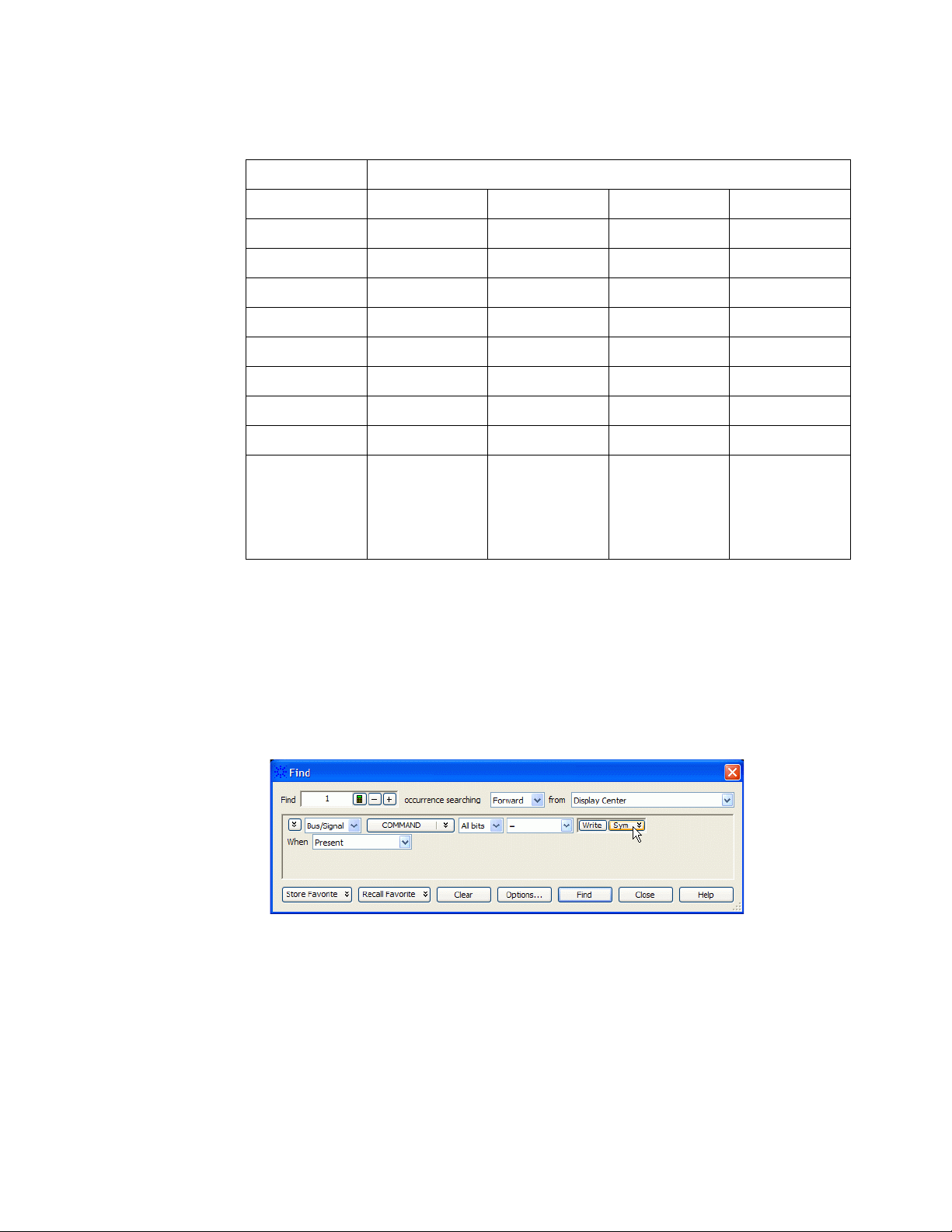
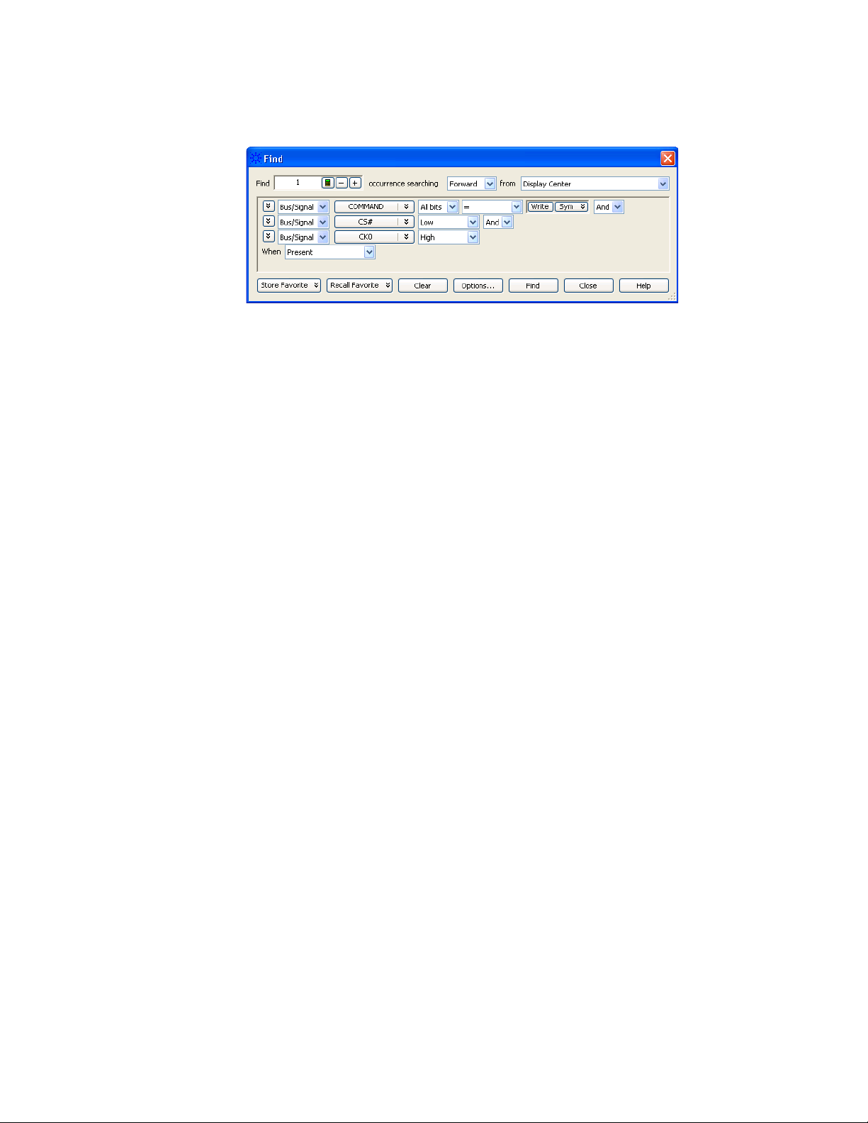
To find commands of a certain type in the listing
1 Open the Find dialog.
2 For the bus/signal name, choose Command.
3 Check that the numeric base is set to Symbol.
4 Select the command you wish to find.
For LPDDR2/LPDDR3, use "CS# = Low" and "CK0 = High" in the search.
50 B4623 LPDDR Bus Decoder User Guide
Page 51
Understanding the Listing 5
B4623 LPDDR Bus Decoder User Guide 51
Page 52
5 Understanding the Listing
Buses Generated by the Decoder
The decoder generates the following columns, which are displayed in the listing in
addition to the input buses.
Physical
Address
DDR Bus
Decode
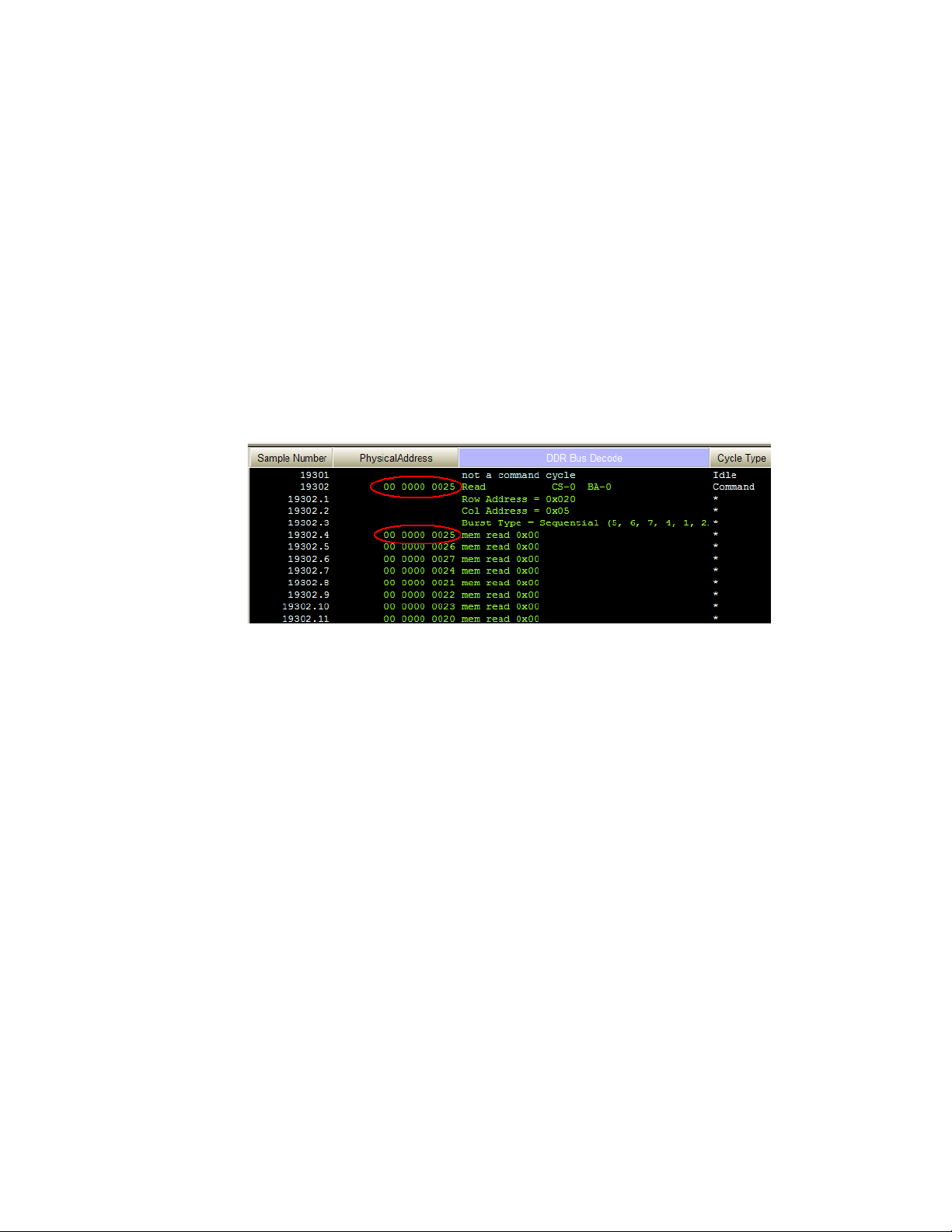
When valid read or write data is present on a DDR cycle, the decoder will display the
full physical address in this column. This address is constructed from the row, column,
and bank address, based on the memory characteristics which were entered in the System
Configuration (see
The initial physical address of a burst is shown in two places: on the main row of the
Read or Write command and on the row of the first read or write. Repeating the value
next to the command allows the value to appear in the Waveform display.
This column contains decoded data from the memory bus. Some of the things which can
be displayed in this column include:
page 19) dialog.
Decoded
commands
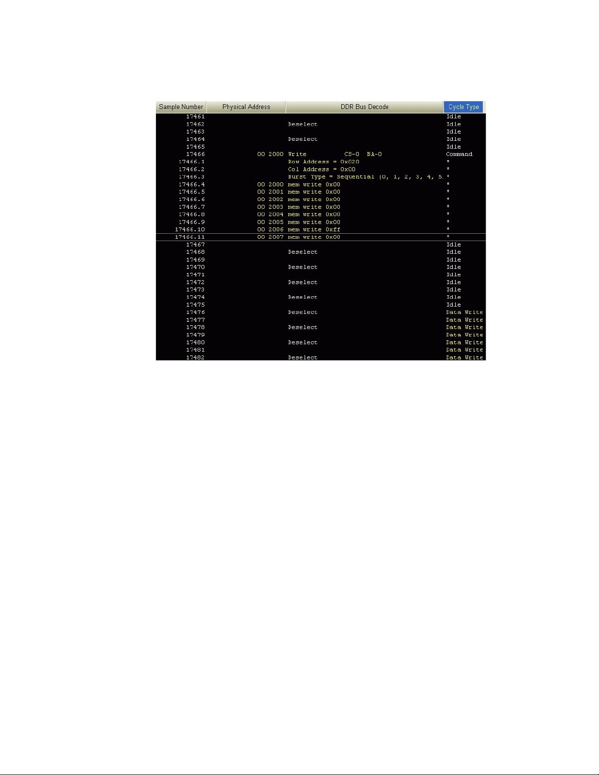
Decoded commands may cover several rows (a main row and several subrows which
appear as part of one state).
In the example below, note that the subrows for th e write (174 66.1-1746 6.11) show data
from the data cycles that are associated with the write (samples 17476 and following).
Note also that these samples are marked as "Data Write" in the Cycle Type column.
52 B4623 LPDDR Bus Decoder User Guide
Page 53
Understanding the Listing 5
Decode Errors An error message is displayed when the decoder can not decode the state. Examples
include:
• "Please enable one or more chip selects"
• "More than one active chip select"
• "Required Buses/Signals are not present"
"Deselect" The message "Deselect" is not an error. It simply indicates states where there is nothing
to decode and the chip selects are not being used (that is, they are deselected). Idle states
are a common example of this.
This message appears only on the rising edge of the clock. The falling edge is left blank,
because no valid command is possible on those states.
Cycle Type The decoder generates a cycle type column which shows summary information about
each state. See
Other buses The following buses and signals are generated by the decoder for its own use. They are
generally not displayed as columns in the listing, but they are visible in some dialogs.
• TAG
See Also •
“Buses and Signals Captured by the Logic Analyzer" on page 46
“Cycle Type" on page 54 for an explanation.
B4623 LPDDR Bus Decoder User Guide 53
Page 54

5 Understanding the Listing
Cycle Type
Cycle Type
columns
Predefined cycle
type symbols
The decoder generates data which identifies the type of memory operation for each state
in the listing. This generated data appears in the listing as the Cycle Type column.
Cycle Type does not appear in the Bus/Signal Setup dialog because it contains
information generated by the decoder, rather than information captured by the logic
analyzer.
Each cycle type value is a 32-bit integer. To avoid any need to interpret these values
yourself, the configuration file defines symbols for each cycle type, such as idle, data
read, or command.
The symbols are:
Bits Meaning
---- ----------------------------------------------------------------
0-3 Command code 0 ==> Mode, 1 ==> Auto, 2 ==> Prechar
ge etc
4 Command 1 ==> command, 0 ==> not command
5 Read 1 ==> read, 0 ==> not read (i.e. write)
6 Data 1 ==> data, 0 ==> not data
7 Subrow 1 ==> subrow 0 ==> not subrow (ie. mainr
ow)
8 Clock disabled 1 ==> clock disabled 0 ==> clock enabled
9 Decode Error 1 ==> decode error 0 ==> not decode error
Symbol Encoding (LS bits) Value Mask
--------------------- ------------------- ----- ---------Decode Error xxxx xx1x xxxx xxxx 200 FFFF FDFF
Clock Disabled xxxx xx01 xxxx xxxx 100 FFFF FC0F
Command & Data xxxx xx00 01x1 xxxx 50 FFFF FC2F
Data xxxx xx00 01xx xxxx 40 FFFF FC3F
Read data xxxx xx00 011x xxxx 60 FFFF FC1F
Write data xxxx xx00 010x xxxx 40 FFFF FC1F
Idle xxxx xx00 00x0 xxxx 00 FFFF FC2F
Command xxxx xx00 0xx1 xxxx 10 FFFF FC6F
Mode Set Command xxxx xx00 0xx1 0000 10 FFFF FC60
Refresh Command xxxx xx00 0xx1 0001 11 FFFF FC60
Precharge Command xxxx xx00 0xx1 0010 12 FFFF FC60
Activate Command xxxx xx00 0xx1 0011 13 FFFF FC60
Write Command xxxx xx00 0xx1 0100 14 FFFF FC60
Read Command xxxx xx00 0xx1 0101 15 FFFF FC60
BST Truncate xxxx xx00 0xx1 0110 16 FFFF FC60
NOP xxxx xx00 0xx1 0110 17 FFFF FC60
* xxxx xx00 1xxx xxxx 80 FFFF FC7F
* R/W Data xxxx xx00 11xx xxxx C0 FFFF FC3F
* R/W Read Data xxxx xx00 111x xxxx E0 FFFF FC1F
Binary Hex Don't Care
54 B4623 LPDDR Bus Decoder User Guide
Page 55
Understanding the Listing 5
* R/W Write Data xxxx xx00 110x xxxx C0 FFFF FC1F
Here are definitions of some of the more general cycle types:
Cycle Type Meaning
Read Data Clock is rising or falling and the data bus
contains valid read data.
Write Data Clock is rising or falling and the data bus
contains valid write data.
Command Clock is rising and a valid command
(possibly Nop) is on the bus.
Idle Clock is rising or falling and the data bus
does not contain valid read/write data.
* Subrows (also called subcycles) are generated
by the decoder to show the data associated
with a command. Each subrow is assigned a
decimal sample number (such as "1234.5").
The order of the
symbols is
important
Using Cycle
Type to filter the
display
Using Cycle
Type to find
data of a certain
type
Decode Error The decoder encountered an error while
decoding the bus. The DDR Bus Decode
column contains information about the cause
of the error.
The first cycle type in this list which matches the value on the Cycle Ty pe bus is the one
which will be displayed.
You can set up a filter to hide states where Cycle Type is "Idle" or some other value you
do not wish to see in the listing. To change the filter settings, see
Chapter 6, “Filtering or
Colorizing the Display,” starting on page 57.
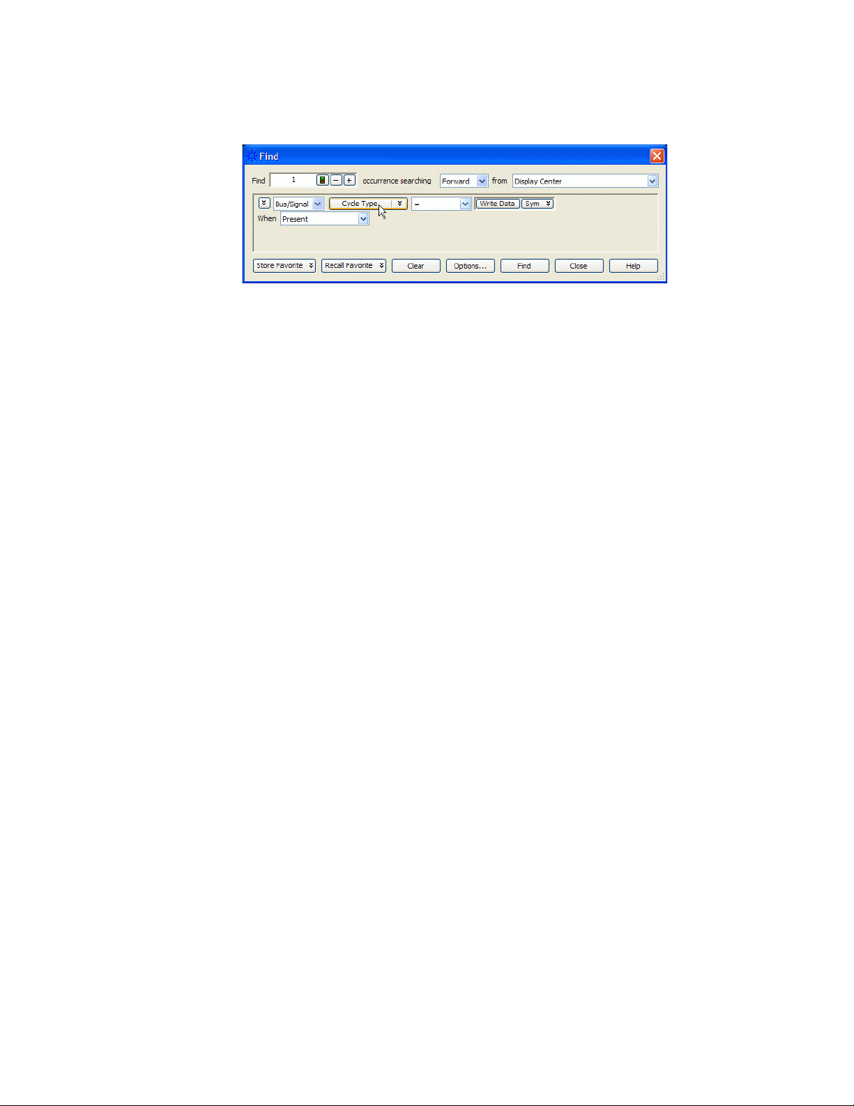
1 Open the Find dialog.
2 Choose Cycle Type bus.
B4623 LPDDR Bus Decoder User Guide 55
Page 56
5 Understanding the Listing
3 Set the numeric base to Symbol.
4 Select the cycle type you wish to find.
56 B4623 LPDDR Bus Decoder User Guide
Page 57

B4623 LPDDR Bus Decoder
User Guide
6
Filtering or Colorizing the Display
The filter tool lets you show or suppress states, based on criteria such as the cycle type or
chip select. You can also display each type of state in a different color.
The filter settings do not affect whether data is stored by the logic analyzer; they only
affect whether that data is displayed or not. You can examine the same data with
different settings, for different analysis requirements.
Filtering allows faster analysis in two ways. First, you can filter unneeded information
out of the display. For example, suppressing idle states will show only states in which a
transaction was completed.
Second, you can isolate particular operations by suppressing all other operations. For
example, you can show just write commands, without the associated data.
T o prevent certain data from being stored, use the logic analyzer's "storage qualification"
(in the online help) feature.
See Also • "The filter/colorize tool" (in the online help)
57
Page 58

6 Filtering or Colorizing the Display
58 B4623 LPDDR Bus Decoder User Guide
Page 59

B4623 LPDDR Bus Decoder
CAUTION
User Guide
7
Troubleshooting the Decoder
If you encounter difficulties while making measurements, use this help topic to guide
you through some possible solutions. Each heading lists a problem you may encounter,
along with some possible solutions.
When you obtain incorrect decoded results, it may be unclear whether the problem is in
the connections, in your device under test, or in the decoder settings. If you follow the
suggestions in this section to ensure that you are using the decoder correctly, you can
proceed with confidence in debugging your device under test.
If you still have difficulty using the analyzer after trying these suggestions, please
contact your Keysight Technologies representative.
When you are working with the analyzer, be sure to power down both the
analyzer and the device under test before disconnecting or connecting cables or
probes. Otherwise, you may damage circuitry in the analyzer or device under
test.
Error messages
Decode Error In the Cycle Type column, this indicates that decoding failed for some reason. See the
DDR Bus Decode column for a description of the error.
"Slow or
Missing Clock"
error
"Add In does
not unattach
from all labels!"
error
• Check that you have loaded the correct configuration file for the probe you are using.
Signals are mapped differently, depending on which configuration file is loaded.
• This error message might occur if the logic analyzer cards are not firmly seated in the
logic analysis system frame. Ensure that the cards are firmly seated.
• This error might occur if the device under test is not running properly . Ensure that t he
device under test is on and operating properly.
• If the error message persists, check that the logic analyzer pods are connected to the
proper connectors.
• This message can occur when you have loaded an .ala configuration file which was saved using a
previous version of the decoder. To update the file to work with a new version of the decoder, see
“To load a configuration file from a previous version of the decoder" on page 19 .
59
Page 60

7 Troubleshooting the Decoder
Slow
performance
Intermittent
data errors
If, just after capturing a trace, the logic analysis system "hangs up" and the following
status message is displayed at the bottom of the screen, the decoder is busy decoding the
captured data.
If the "Processing" message doesn't go away after a minute or two, it is possible that the
decoder is searching through an enormous number of idle states in between
"meaningful" states.
• Use the Cancel button to stop the decoder.
This problem is usually caused by poor connections, incorrect signal levels, or marginal
timing.
• Remove and re-seat all cables and probes, ensuring that there are no bent pins or
poor probe connections.
No activity on
activity
indicators
No trace list
display
• Adjust the threshold level of the data pod to match the logic levels in the system
under test.
• Use an oscilloscope to check the signal integrity of the data lines.
• Clock signals for the state analyzer must meet particular pulse shape and timing
requirements. Data inputs for the analyzer must meet pulse shape and setup and hold
time requirements.
• Check the sampling positions (see
See also Capacitive loading (see
data errors.
• Check for loose cables.
• Check for bent or damaged pins.
If there is no trace list display, it may be that your trigger specification is not correct for
the data you want to capture, or that the trace memory is only partially filled.
• Check your trigger sequence to ensure that it will capture the events of interest.
• Try stopping the analyzer; if the trace list is partially filled, this should display the
contents of trace memory.
page 22).
page 61) for information on other sources of intermittent
60 B4623 LPDDR Bus Decoder User Guide
Page 61

Troubleshooting the Decoder 7
Analyzer won't
power up
Erratic trace
measurements
Capacitive
loading
If logic analyzer power is cycled when the logic analyzer is connected to a device under
test that remains powered up, the logic analyzer may not be able to power up. Some logic
analyzers are inhibited from powering up when they are connected to a device under test
that is already powered up.
• Remove power from the device un der test, then disconnect all logic analyzer cabling.
This will allow the logic analyzer to power up. Reconnect logic analyzer cabling after
power up.
• Do a full reset of the device under test before beginning the measurement.
• Ensure that your device under test meets the timing requirements of the applicable
JEDEC bus standard.
• See Capacitive loading (see
close timing margins, loading from probes may cause incorrect functioning and give
erratic trace results.
• Ensure that you have sufficient cooling for the device under test while the probes are
installed.
Excessive capacitive loading can degrade signals, resulting in incorrect capture, or
system lockup in the microprocessor. All probes add additional capacitive loading, as
can custom probe fixtures you design for your application.
Careful layout of your device under test can minimize loading problems and result in
better margins for your design. This is especially important for systems that are running
at frequencies greater than 50 MHz.
Remove as many pin protectors, extenders, and adapters as possible.
page 61). If the device under test design has extremely
No decoding or
incorrect
decoding
Decoder will not
load or run
This problem may be due to incorrect synchronization, modified configuration, incorrect
connections, or a hardware problem in the device under test. A locked status line can
cause incorrect or incomplete decoding.
• Ensure that each logic analyzer pod is connected to the correct connector.
There is not always a one-to-one correspondence between analyzer pod numbers and
connector numbers. Probes must supply address, data, and status information to the
analyzer in a predefined order.
• Check the activity indicators for status lines locked in a high or low state.
• Check that the signals on the device under test are routed to the connector according
to the manual for your probe.
• Verify that the required input buses have not been modified from their default values.
These buses must remain as they are configured by the configuration file. Do not
change the names of these labels or the bit assignments within the labels. Some
analysis probes also require other data labels.
• Verify that storage qualification has not excluded storage of all the needed states.
• Verify that you have correctly configured the sampling positions.
• Ensure that you have the correct software loaded on your analyzer .
B4623 LPDDR Bus Decoder User Guide 61
Page 62

7 Troubleshooting the Decoder
• Configuration files for the state analyzer contain a pointer to the name of the
corresponding inverse assembler or decoder. If you delete the decoder or rename it,
the configuration process will fail to load the decoder.
62 B4623 LPDDR Bus Decoder User Guide
Page 63
B4623 LPDDR Bus Decoder
User Guide
A
Customizing Physical Address
Construction
When to
Customize the
Physical
Address
Construction
Algorithm
To create a
custom
algorithm
DDR memory systems use rank, bank address, row address and column address to
construct a physical memory address. The algorithm for converting BA, RA and CA to
physical address is implementation dependent. If your system constructs addresses using
an order other than {BA,RA,CA}, you neet to provide an algorithm to translate the bits
which the logic analyzer captures into the BA, RA, and CA values. This algorithm is in
the form of a .NET assembly .dll.
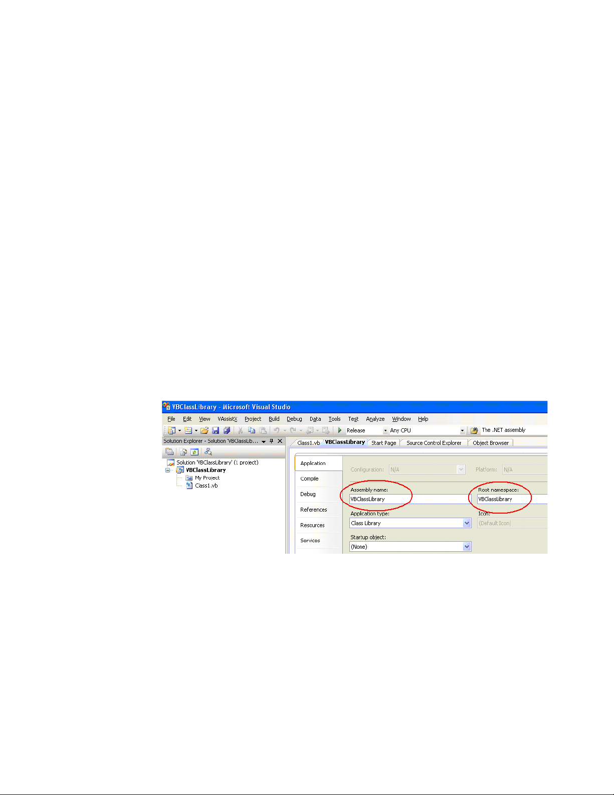
1 Create a Microsoft Visual Studio 2008 .NET assembly:
• Use the class "DDRtoPhysical", which implements the methods described below.
• The assembly name and the namespace are user defined but must be identical.
2 Select the "User supplied .NET assembly" button in the System Configuration dialog
and specify the location of the .dll file you created. The default location is
C:\Program Files\Keysight Technologies\Logic Analyzer\
DDRtoPhysical.dll
If the user has selected "User supplied .NET assembly" and the specified .dll does not
exist; the user will get the following error message when he closes the System
Configuration dialog.
The .NET assembly could not be found or is incorrect.
Physical Addresses will not be displayed
63
Page 64

A Customizing Physical Address Construction
Methods in the
.NET assembly
AddressTranslat
ionInit ()
The
method
bool AddressTranslationInit(CString strToolName, __int16 & nNumberOfBit
s)
Each DDR decoder on the LA workspace will call this method when it is initialized with
a configuration file, or when the "OK" button is pressed in the "System Configuration"
dialog.
Note: This means that the method may be called multiple times with the same
ToolName. The method must tolerate this without an error return.
The .dll will use this method as an opportunity to display a GUI for the user to set
assorted configuration parameters that will be used in the PhysicalAddress method such
as number of row bits, number of column bits and number of bank address bits etc.
strToolName = Unicode string, The name of the DDR Bus decode tool. Since it is
possible for the user to have multiple memory systems, each with it's own DDR bus
decode tool, it is necessary to tell the AddressTranslationInit () method and the
PhysicalAddress() method which instance of the DDR bus decoder is making the
request; e.g. In the following example there are two instances of the bus decoder. One is
called 'DDR Bus Decoder-1' and one is called 'DDR Bus Decoder-2'. Note: it is the
responsibility of the .dll to maintain a data structure of each call to
AddressTranslationInit (); i.e. for each strToolName.
nNumberOfBits = Return value: number of bits of physical address to be displayed by
the decoder.
The
PhysicalAddress
() method
If the call to the method throws an exception (method does not exist, parameter list is
wrong etc.) the decoder will display the following error message and will display all
subsequent physical address as <blank>.
Unable to invoke member AddressTranslationInit().
Physical Addresses will not be displayed
If the call to the method succeeds but the method returns false, the decoder will display
the following error message and will display all subsequent physical address as <blank>.
DDRtoPhysical::AddressTranslationInit() returned false.
Physical Addresses will not be displayed
The decoder proceeds with decode, displaying all Physical Addresses as <blank>. In this
case, the decoder will never call the PhysicalAddress() method. Note: we display
<blank> rather than "unknown" because the Physical Address label is a numeric label,
not a string label.
bool PhysicalAddress ( CString strToolName,
__int16 RankAdd,
__int16 BankAddr,
__int16 RowAddr,
__int16 ColAddr,
__int64 & PhysicalAddress)
64 B4623 LPDDR Bus Decoder User Guide
Page 65

Customizing Physical Address Construction A
If the user has selected "User supplied .NET assembly", the DDR tool will call this
method each time it needs to compute a physical address.
strToolName = The tool name as described above in the Init() method. The
PhysicalAddress() method may choose to ignore this parameter, or it may use it to apply
a unique algorithm based on the tool name and its associated AddressTranslationInit ().
RankAddr = Rank address
BankAddr = Bank address bits
RowAddr = Address bus for applicable activate command
ColAddr = Address bus for applicable R/W command
PhysicalAddress = return value
If the call to the method throws an exception (method does not exist, parameter list is
wrong etc.) the decoder will display the following error message and will display all
subsequent physical address as <blank>.
Unable to Invoke member PhysicalAddress().
Physical Addresses will not be displayed
The
BusAddress()
method
If the call to the method succeeds but the method returns false, the decoder will display
the following error message and will display all subsequent physical address as <blank>.
DDRtoPhysical::PhysicalAddress() returned false.
Physical Addresses will not be displayed
bool BusAddress ( CString strToolName,
__int16 &RankAdd,
__int16 &BankAddr,
__int16 &RowAddr,
__int16 &ColAddr,
__int64 PhysicalAddress)
This is an optional method. If it exists and if the user has selected "User supplied .NET
assembly", the method will be used by the Address Co nv ersio n too l to conv ert ph ysical
addresses to bus addresses.
strT oolName = The tool name as described above in the Init() method. The BusAddress()
method may choose to ignore this parameter, or it may use it to apply a unique algorithm
based on the tool name and its associated AddressTranslationInit ().
RankAddr = Return Value
BankAddr = Return Value
RowAddr = Return Value
ColAddr = Return Value
PhysicalAddress = Physical address to be converted to Rank, Bank, Row, Column
B4623 LPDDR Bus Decoder User Guide 65
Page 66

A Customizing Physical Address Construction
If the call to the method throws an exception (method does not exist, parameter list is
wrong etc.) the decoder will display the following error message and all controls in the
Address Conversion dialog will be disabled.
Unable to Invoke member BusAddress().
Address Conversion dialog disabled
If the call to the method succeeds but the method returns false, the decoder will display
the following error message.
DDRtoPhysical::BusAddress() returned false.
Address Conversion dialog disabled
NameChanged()
DDRtoPhysical
The
method
Sample
class
bool NameChanged ( CString strOldToolName, CString strNewToolName)
This method will be called whenever the user changes the name of the bus decoder in the
overview. The method is also called when loading a config file. In this case, the
OldToolName and the NewToolName are identical.
If the call to the method throws an exception (method does not exist, parameter list is
wrong etc.) the decoder will display the following error message and will display all
subsequent physical address as <blank>.
Unable to Invoke member NameChanged().
Physical Addresses will not be displayed
If the call to the method succeeds but the method returns false, the decoder will display
the following error message and will display all subsequent physical address as <blank>.
DDRtoPhysical::NameChanged() returned false.
Physical Addresses will not be displayed
Public Class DDRtoPhysical
Public Function AddressTranslationInit(ByVal strToolNameAsString, _
ByRef nNumberOfBitsAsInt16) AsBoolean
MsgBox("In AddressTranslationInit. ToolName="&strToolName)
nNumberOfBits = 48
Return True
End Function
Public Function PhysicalAddress(ByVal strToolNameAsString, _
ByVal nRankAddrAsInt16, ByVal nBankAddrAsInt16, _
ByVal nRowAddrAsInt16, ByVal nColAddrAsInt16, _
ByRef nAddressAsInt64) AsBoolean
nAddress = nRankAddr + nBankAddr + nRowAddr + nColAddr
Return True
End Function
66 B4623 LPDDR Bus Decoder User Guide
Page 67

Customizing Physical Address Construction A
Public Function BusAddress(ByVal strToolNameAsString, _
ByRef nRankAddrAsInt16, ByRef nBankAddrAsInt16, _
ByRef nRowAddrAsInt16, ByRef nColAddrAsInt16, _
ByVal nAddressAsInt64) AsBoolean
nRankAddr = nAddress + 1
nBankAddr = nAddress + 2
nRowAddr = nAddress + 3
nColAddr = nAddress + 4
Return True
End Function
Public Function NameChanged(ByVal strToolOldNameAsString, _
ByVal strToolNewNameAsString) AsBoolean
MsgBox("In NameChanged: Old name ="&strToolOldName & _
" New name = " & strToolNewName)
Return True
End Function
End Class
B4623 LPDDR Bus Decoder User Guide 67
Page 68

A Customizing Physical Address Construction
68 B4623 LPDDR Bus Decoder User Guide
Page 69

Index
Symbols
# in listing, 45
B
B4623B LPDDR bus decoder, 7
Buses and signals captured by the logic
analyzer, 46, 52
C
clock qualifiers, 35
COLADDR[0], 21
color, decoder listing, 57
configuration file, loading, 17
configuration file, loading from previous
version, 19
Cycle Type, 54
D
Deselect, 52
E
errors, 59
problems, 59
S
self refresh, 35
slow or missing clock error, 59
Source bus, 52
T
Tag Bits, 54
trigger, LPDDR, 43
trigger, unwanted, 59
troubleshooting, 59
U
Understanding the Decoded Listing, 45
W
W2637A LPDDR x16 BGA probe, 7
W2638A LPDDR x32 BGA probe, 7
F
filtering the LPDDR display, 57
L
license, LPDDR bus decoder, 11
LPDDR, 7
LPDDR bus decoder, 7
LPDDR bus decoder, configuring, 17
LPDDR bus decoder, installing
software, 11
LPDDR bus overview, 7
LPDDR data, capturing, 43
LPDDR device under test, connecting
to, 16
LPDDR properties, 19
LPDDR1, 7
LPDDR2, 7
P
power down, 35, 38
B4623 LPDDR Bus Decoder User Guide 69
Page 70

Index
70 B4623 LPDDR Bus Decoder User Guide
 Loading...