

Page 1
www.DataSheet4U.com
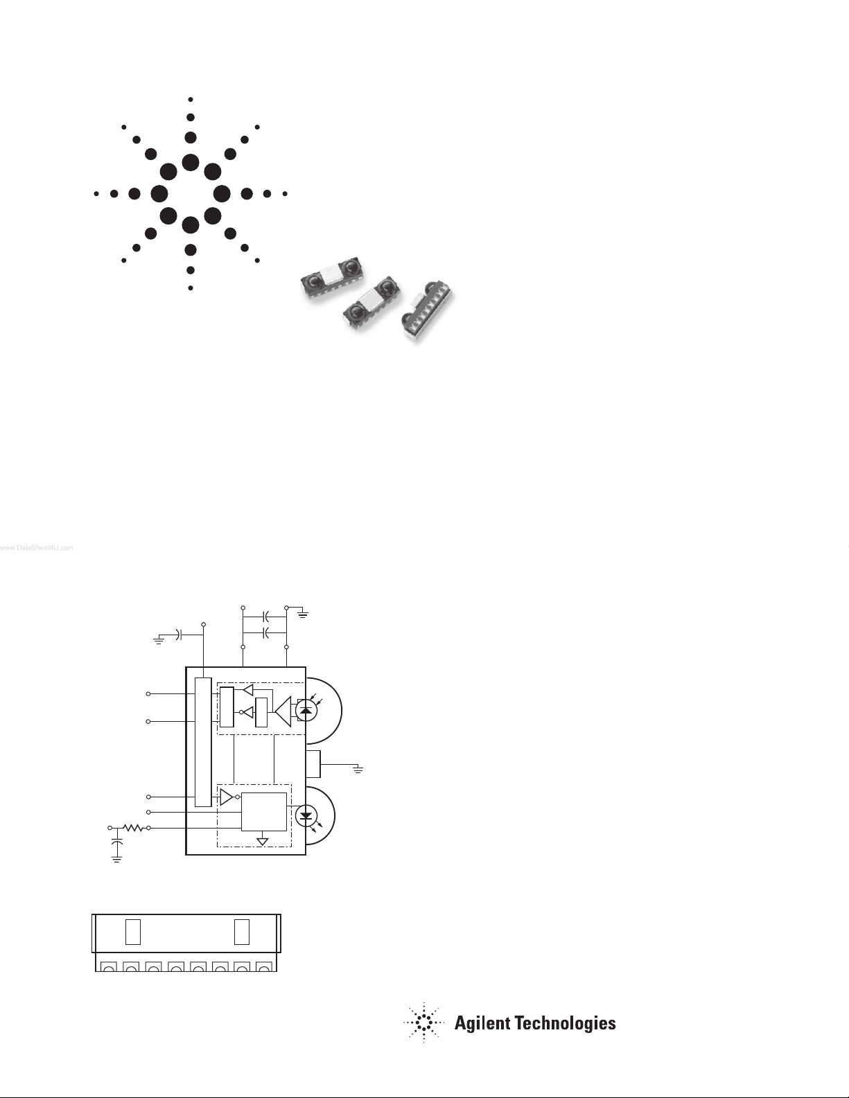
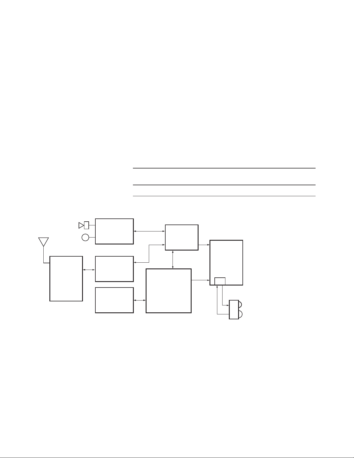
Description
The HSDL-3220 is a new
generation low profile high speed
infrared transceiver module that
provides interface between logic
and IR signals for through-air,
serial, half-duplex IR data-link.
The module is fully compliant to
IrDA Physical Layer specification
version 1.4 low power from
9.6kbit/s to 4.0 Mbit/s (FIR) and
is IEC825-Class 1 Eye Safe.
V
CX2
CC
CX4
CX1
V
(6)
IOV
SD (5)
RXD (4)
TXD (3)
LED C (2)
R1
V
led
Figure 1. Functional block diagram of HSDL-3220.
LED A (1)
CX3
CC
(7)
CC
HSDL-3220
TRANSMITTER
GND (8)
RECEIVER
Agilent HSDL-3220 IrDA
®
Data Compliant Low Power
4.0 Mbit/s Infrared Transceiver
Data Sheet
Features
•
Fully compliant to IrDA 1.4 physical
layer low power specification from
9.6 kbit/s to 4.0 Mbit/s (FIR)
• Miniature package
– Height: 2.5 mm
– Width: 8.0 mm
– Depth: 3.0 mm
• Typical link distance > 50 cm
Guaranteed temperature performance,
•
o
to 70oC
-25
•
The HSDL-3220 can be shutdown
completely to achieve very low
power consumption. In the
shutdown mode, the PIN diode
will be inactive and thus producing very little photocurrent even
under very bright ambient light.
It is also designed to interface to
input/output logic circuits as low
as 1.8V. These features are ideal
for mobile devices that require
low power consumption.
SHIELD
Critical parameters are guaranteed over
temperature and supply voltage
• Low power consumption
Low shutdown current
–
– Complete shutdown of TXD, RXD,
and PIN diode
• Excellent EMI performance
• Vcc supply 2.7 to 3.6 Volts
• Interfacing with I/O logic circuits as
low as 1.8 V
• Lead-free package
• LED stuck-high protection
• Designed to accommodate light loss
with cosmetic windows
• IEC 825-class 1 eye safe
• Lead-free and RoHS Compliant
Applications
• Mobile telecom
– Mobile phones
– Smart phones
– Pagers
• Data communication
– Pocket PC handheld products
– Personal digital assistants
– Portable printers
• Digital imaging
– Digital cameras
– Photo-imaging printers
• Electronic wallet
• Small industrial & medical
instrumentation
– General data collection devices
– Patient & pharmaceutical data
collection devices
1
2
3
4
5
6
7
8
Figure 2. Rear view diagram with pinout.
Page 2

Application Support Information
The Application Engineering
Group is available to assist you
with the application design
associated with the HSDL -3220
infrared transceiver module. You
can contact them through your
local sales representatives for
additional details.
Order Information
Part Number Packaging Type Package Quantity
HSDL-3220-021 Tape and Reel Front View 2500
HSDL-3220-001 Tape and Reel Front View 500
I/O Pins Configuration Table
Pin Symbol Description I/O Type Notes
1 LED A LED Anode I 1
2 LED C LED Cathode 2
3 TXD Transmit Data. Active High. I 3
4 RXD Receive Data. Active Low. O 4
5 SD Shutdown. Active High. I 5
6 Vcc Supply Voltage 6
7 IOVcc Input/Output ASIC Vcc 7
8 GND Ground 8
- Shield EMI Shield 9
Marking Information
The unit is marked with the
letter “G” and “YWWLL” on the
shield where:
Y is the last digit of the year
WW is the work week
LL is the lot information
Recommended Application Circuit Components
Component Recommended Value Notes
R1 5.6Ω ± 5%, 0.25 watt for 2.7 ≤ Vled <3.3V
10Ω ± 5%, 0.25 watt for 3.3 ≤ Vled <4.2V
15Ω ± 5%, 0.25 watt for 4.2 ≤ Vled < 5.5V
CX1, CX4 0.47 µF ± 20%, X7R Ceramic 10
CX2, CX3 6.8 µF ± 20%, Tantalum 11
Notes:
1. Tied through external series resistor, R1, to regulated Vled from 2.7 to 5.5V. Please refer to table
above for recommended series resistor value.
2. Internally connected to LED driver. Leave this pin unconnected.
3. This pin is used to transmit serial data when SD pin is low. If this pin is held high for longer than
50 µs, the LED is turned off. Do NOT float this pin.
4. This pin is capable of driving a standard CMOS or TTL load. No external pull-up or pull-down
resistor is required. The pin is in tri-state when the transceiver is in shutdown mode. The receiver
output echoes transmitted signal.
5. The transceiver is in shutdown mode if this pin is high for more than 400 µs. On falling edge of
this signal, the state of the TXD pin sampled and used to set receiver low bandwidth (TXD=low)
or high bandwidth (TXD=high) mode. Refer to the section ”Bandwidth selection timing” for
programming information. Do NOT float this pin.
6. Regulated, 2.7 to 3.6 Volts.
7. Connect to ASIC logic controller Vcc voltage or supply voltage. The voltage at this pin must be
equal to or less than supply voltage.
8. Connect to system ground.
9. Connect to system ground via a low inductance trace. For best performance, do not connect
directly to the transceiver pin GND.
10. CX1 must be placed within 0.7 cm of the HSDL-3220 to obtain optimum noise immunity.
11. In environments with noisy power supplies, including CX2, as shown in Figure 1, can enhance
supply ripple rejection performance.
2
Page 3
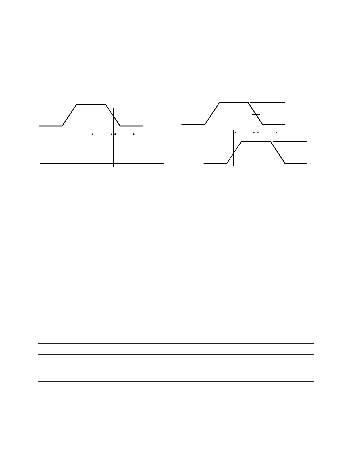
Bandwidth Selection Timing
The transceiver is in default SIR/
MIR mode when powered on.
User needs to apply the following
programming sequence to both
the SD and TXD inputs to enable
the transceiver to operate at FIR
mode.
SD/MODE
t
S
50%
V
V
IH
SD/MODE
V
IL
t
H
t
S
50%
t
H
IH
V
IL
V
IH
50%50%TXD
V
IL
Figure 3. Bandwidth selection timing at SIR/MIR mode. Figure 4. Bandwidth selection timing at FIR mode.
Setting the transceiver to SIR/MIR
Mode (9.6 kbit/s to 1.152 Mbit/s)
1. Set SD/Mode input to logic
HIGH
2. TXD input should remain at
logic LOW
3. After waiting for t
≥ 25 ns, set
S
SD/Mode to logic LOW, the
HIGH to LOW negative edge
transition will determine the
receiver bandwidth
4. Ensure that TXD input remains low for tH ≥ 100 ns, the
receiver is now in SIR/MIR
mode
5. SD input pulse width for mode
selection should be > 50 ns.
Setting the transceiver to FIR
(4.0 Mbit/s) Mode
1. Set SD/Mode input to logic
HIGH
2. After SD/Mode input remains
HIGH at > 25 ns, set TXD input
to logic HIGH, wait tS ≥ 25 ns
(from 50% of TXD rising edge
till 50% of SD falling edge)
3. Then set SD/Mode to logic
LOW, the HIGH to LOW
negative edge transition will
determine the receiver bandwidth
4. After waiting for tH ≥ 100 ns,
set the TXD input to logic LOW
5. SD input pulse width mode
selection should be > 50 ns.
Transceiver I/O Truth Table
50%50%TXD
V
IL
Inputs Outputs
TXD Light Input to Receiver SD LED RXD Note
High Don’t Care Low On Not Valid
Low High Low Off Low 12,13
Low Low Low Off High
Don’t Care Don’t Care High Off High
Notes:
12. In-band IrDA signals and data rates ≤ 4.0 Mbit/s
13. RXD logic low is a pulsed response. The condition is maintained for a duration dependent on pattern and strength of the incident intensity.
3
Page 4
CAUTIONS: The BiCMOS inherent to the design of this component increases the component’s
susceptibility to damage from electrostatic discharge (ESD). It is advised that normal static precautions
be taken in handling and assembly of this component to prevent damage and/or degradation which may
be induced by ESD.
Absolute Maximum Ratings
For implementations where case to ambient thermal resistance is ≤50°C/W.
Parameter Symbol Min. Max. Units Conditions
Storage Temperature T
Operating Temperature T
LED Anode Voltage V
Supply Voltage V
Input Voltage: TXD, SD/Mode V
Output Voltage: RXD V
DC LED Transmit Current I
Average Transmit Current I
S
A
LEDA
CC
I
O
(DC) 50 mA
LED
(PK) 200 mA ≤90 µs pulse width
LED
-40 +100 °C
-25 +70 °C
0 6.5 V
0 6.5 V
0 6.5 V
0 6.5 V
≤25% duty cycle
Recommended Operating Conditions
Parameter Symbol Min. Typ. Max. Units Conditions
Supply Voltage V
CC
Input/Output Voltage IOVcc 1.8 Vcc V
Logic Input Voltage
for TXD, SD/Mode
Logic High V
Logic Low V
Logic High
IH
IL
E
IH, min
Receiver Input Irradiance 0.020 mW/cm
E
IH, max
Logic Low E
LED (Logic High) Current I
Pulse Amplitude
IL
LEDA
Receiver Data Rate 0.0096 4.0 Mbit/s
Note :
14. An in-band optical signal is a pulse/sequence where the peak wavelength, λp, is defined as 850 ≤ λp ≤ 900 nm, and the pulse characteristics are
compliant with the IrDA Serial Infrared Physical Layer Link Specification v1.4.
2.7 3.6 V
IOVcc – 0.5 IOV
cc
0 0.4 V
0.0081 mW/cm
500 mW/cm
0.3 µW/cm
150 mA
V
2
9.6kbit/s ≤ in-band signals
≤1.152 Mbit/s
2
1.152 Mbit/s < in-band signals
≤ 4.0 Mbit/s
2
9.6 kbit/s ≤ in-band signals
≤ 4.0 Mbit/s
2
For in-band signals
[14]
[14]
[14]
[14]
4
Page 5

Electrical and Optical Specifications
Specifications (Min. and Max. values) hold over the recommended operating conditions unless otherwise noted.
Unspecified test conditions may be anywhere in their operating range. All typical values (Typ.) are at 25°C, Vcc set to 3.0V
and IOVcc set to 1.8V unless otherwise noted.
Parameter Symbol Min. Typ. Max. Units Conditions
Receiver
Viewing Angle 2θ 30 °
Peak Sensitivity Wavelength λp 880 nm
RXD Output Voltage
Logic High V
Logic Low V
RXD Pulse Width (SIR)
RXD Pulse Width (MIR)
RXD Pulse Width (FIR)
[15]
[16]
[16]
tPW (SIR) 1 4.0 µs θ ≤ 15°, CL = 9 pF
tPW(MIR) 100 500 ns θ ≤ 15°, CL = 9 pF
tPW(FIR) 80 175 ns θ ≤ 15°, CL = 9 pF
RXD Rise and Fall Times tr, t
Receiver Latency Time
Receiver Wake Up Time
[17]
[18]
t
L
t
W
OH
OL
IOVCC – 0.2 IOV
0 0.4 V I
f
60 ns CL = 9 pF
VI
CC
= -200 µA, EI ≤ 0.3 µW/cm
OH
= 200 µA, EI ≥ 8.1 µW/cm
OL
25 50 µs
50 100 µs
2
2
Transmitter
Radiant Intensity IE
H
10 45 mW/sr I
= 150 mA, θ ≤ 15°, V
LEDA
V
≤ VIL, Ta=25°C
SD
TXD
≥ VIH,
Viewing Angle 2θ 30 60 °
Peak Wavelength λ
p
875 nm
Spectral Line Half Width ∆λ 35 nm
TXD Input Current
High I
Low I
LED ON Current I
H
L
LEDA
150 mA V
10 µAV
10 µA0 ≤ V
TXD Pulse Width (SIR) tPW (SIR) 1.5 1.6 1.8 µst
≥ V
TXD
IH
≤ V
TXD
IL
≥ VIH, R1=5.6ohm, Vled=3.0V
TXD
(TXD) = 1.6 µs at 115.2 kbit/s
PW
TXD Pulse Width (MIR) tPW(MIR) 148 217 260 ns tPW (TXD) = 217 ns at 1.152 Mbit/s
TXD Pulse Width (FIR) tPW(FIR) 115 125 135 ns tPW(TXD)=125 ns at 4.0 Mbit/s
Maximum Optical PW
TXD Rise and fall Time (Optical) t
[19]
t
PW(max.)
, t
r
f
50 100 µs
600 ns tPW(TXD) = 1.4 µs at 115.2 kbit/s
40 ns tPW (TXD) = 125 ns at 4.0 Mbit/s
LED Anode On-State Voltage V
ON(LEDA)
1.6 2.1 V I
=150 mA, V
LEDA
TXD≥VIH
Transceiver
Supply Current Shutdown I
Idle I
Notes:
15. For in-band signals from 9.6 kbit/s to 115.2 kbit/s, where 9 µW/cm
16. For in-band signals from 0.576 Mbit/s to 4.0 Mbit/s, where 22.5 µW/cm
17. Latency time is defined as the time from the last TxD light output pulse until the receiver has recovered full sensitivity.
18. Receiver wake up time is measured from Vcc power on or SD pin high to low transition to a valid RXD output.
19. The maximum optical PW is the maximum time the LED remains on when the TXD is constantly high. This is to prevent long turn on time of the LED
for eye safety protection.
CC1
CC2
0.1 1 µAV
≥ V
SD
1.8 3.0 mA VSD ≤ VIL, V
2
≤ EI ≤ 500 mW/cm2.
2
≤ EI ≤ 500 mW/cm2.
Ta= 25°C
IH,
TXD
≤ VIL, EI=0
5
Page 6
t
t
V
OH
V
OL
90%
50%
10%
pw
LED ON
LED OFF
90%
50%
10%
pw
t
f
t
r
t
r
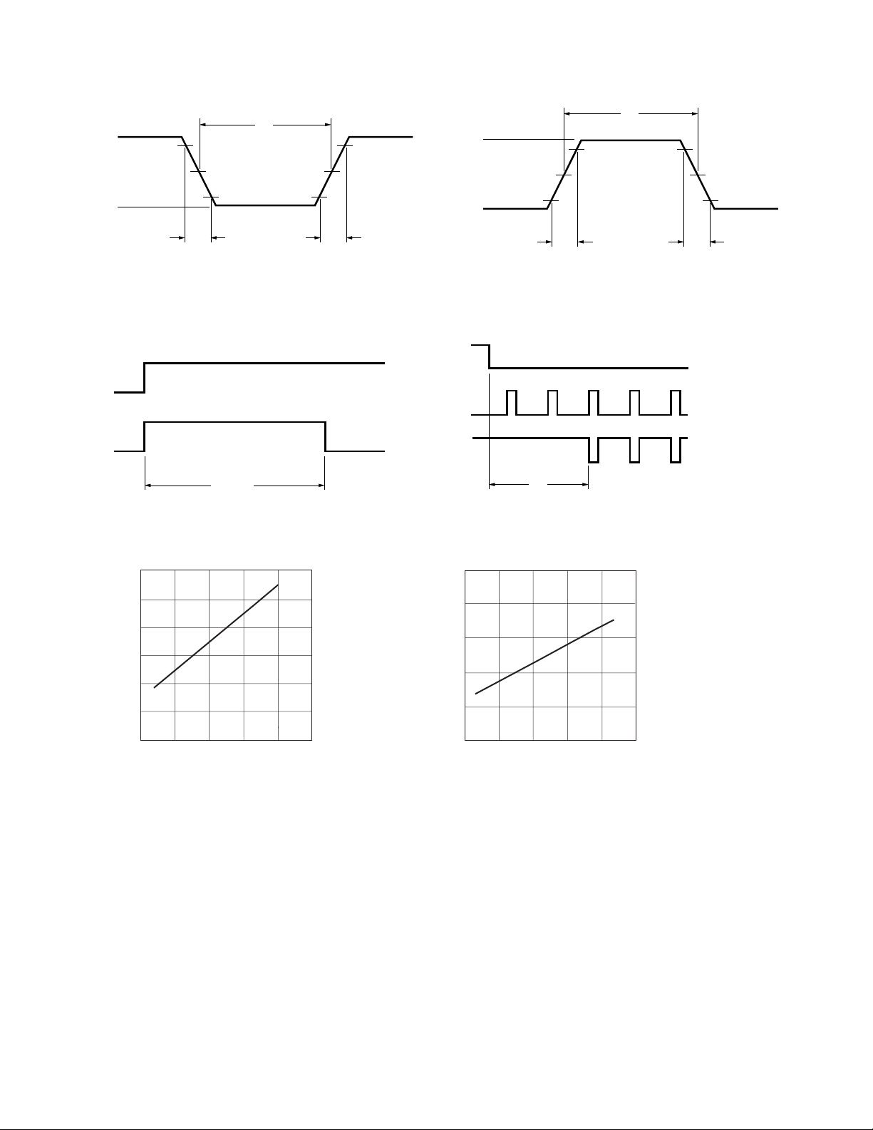
Figure 5. RxD output waveform. Figure 6. LED optical waveform.
SD
TXD
RX
LIGHT
LED
t
pw (MAX.)
RXD
t
RW
Figure 8. Receiver wakeup time waveform.Figure 7. TxD “Stuck On” protection waveform.
120
100
80
60
40
RADIANT INTENSITY (mW/sr)
20
(V)
LEDA
V
2.4
2.2
2.0
1.8
1.6
t
f
0
0.10 0.200.15 0.30 0.350.25
Figure 9. Radiant Intensity vs I
6
I
LEDA
(A)
LEDA
1.4
0.10 0.200.15 0.30 0.350.25
I
(A)
LEDA
.
Figure 10. V
LEDA
vs I
LEDA
.
Page 7
HSDL-3220 Package Dimensions
0.8
2.0
0.4
7
Page 8

HSDL-3220 Tape and Reel Dimensions
Unit: mm
POLARITY
0.4 ± 0.05
2.8 ± 0.1
Empty
(40 mm min)
Pin 8: VLED
Pin 1: GND
4.0 ± 0.1
+0.1
Ø1.5
0
8.4 ± 0.1
3.4 ± 0.1
Progressive Direction
Parts Mounted Leader
1.5 ± 0.1
8.0 ± 0.1
(400 mm min)
Empty
(40 mm min)
1.75 ± 0.1
7.5 ± 0.1
16.0 ± 0.2
Option # "B"
"C"
178 60
330 80 2500021
Unit: mm
Detail A
2.0 ± 0.5
13.0 ± 0.5
LABEL
21 ± 0.8
Detail A
Note: The carrier tape is compliant to the packaging materials standards for ESD sensitive device, EIA-541
Quantity
500001
R1.0
BC
+2
16.4
0
2.0 ± 0.5
8
Page 9

Moisture Proof Packaging
All HSDL-3220 options are
shipped in moisture proof
package. Once opened, moisture
absorption begins.
This part is compliant to JEDEC
Level 4.
Baking Conditions
If the parts are not stored in dry
conditions, they must be baked
before reflow to prevent damage
to the parts.
Package Temp. Time
NO BAKING
IS NECESSARY
YES
UNITS IN A SEALED
MOISTURE-PROOF
PACKAGE
PACKAGE IS
OPENED (UNSEALED)
ENVIRONMENT
LESS THAN 30°C,
AND LESS THAN
60% RH
YES
PACKAGE IS
OPENED LESS
THAN 72 HOURS
NO
In reels 60°C ≥ 48 hours
In bulk 100°C ≥ 4 hours
125°C ≥ 2 hours
150°C ≥ 1 hour
Baking should only be done once.
Recommended Storage Conditions
Storage Temperature 10°C to 30°C
Relative Humidity below 60% RH
Time from Unsealing to Soldering
After removal from the bag, the
parts should be soldered within
three days if stored at the recommended storage conditions. If
times longer than three days are
needed, the parts must be stored
in a dry box.
Figure 11. Baking conditions chart.
PERFORM RECOMMENDED
BAKING CONDITIONS
NO
9
Page 10
Recommended Reflow Profile
0
255
230
220
200
180
160
120
T – TEMPERATURE – (°C)
R1
80
25
0
P1
HEAT
UP
R2
50 150100 200 250 30
t-TIME (SECONDS)
P2
SOLDER PASTE DRY
MAX. 260°C
R3
60 sec.
MAX.
ABOVE
220°C
P3
SOLDER
REFLOW
R4
COOL DOWN
R5
P4
Process Zone Symbol ∆T Maximum ∆T/∆time
Heat Up P1, R1 25°C to 160°C4°C/s
Solder Paste Dry P2, R2 160°C to 200°C 0.5°C/s
Solder Reflow
Cool Down P4, R5 200°C to 25°C-6°C/s
P3, R3 200°C to 255°C (260°C at 10 seconds max) 4°C/s
P3, R4 255°C to 200°C-6°C/s
The reflow profile is a straightline representation of a nominal
temperature profile for a convective reflow solder process. The
temperature profile is divided
into four process zones, each with
different ∆T/∆time temperature
change rates. The ∆T/∆time rates
are detailed in the above table.
The temperatures are measured
at the component to printed
circuit board connections.
In process zone P1, the PC board
and HSDL-3220 castellation pins
are heated to a temperature of
160°C to activate the f lux in the
solder paste. The temperature
ramp up rate, R1, is limited to
4°C per second to allow for even
heating of both the PC board and
HSDL-3220 castellations.
Process zone P2 should be of
sufficient time duration (60 to
120 seconds) to dry the solder
paste. The temperature is raised
to a level just below the liquidus
point of the solder, usually 200°C
(392°F).
Process zone P3 is the solder
reflow zone. In zone P3, the
temperature is quickly raised
above the liquidus point of solder
to 255° C (491° F) for optimum
results. The dwell time above the
liquidus point of solder should be
between 20 and 60 seconds. It
usually takes about 20 seconds to
assure proper coalescing of the
solder balls into liquid solder and
the formation of good solder
connections. Beyond a dwell time
of 60 seconds, the intermetallic
growth within the solder connections becomes excessive, resulting in the formation of weak and
unreliable connections. The
temperature is then rapidly
reduced to a point below the
solidus temperature of the
solder, usually 200°C (392° F), to
allow the solder within the
connections to freeze solid.
Process zone P4 is the cool down
after solder freeze. The cool down
rate, R5, from the liquidus point
of the solder to 25°C (77° F)
should not exceed 6°C per second
maximum. This limitation is
necessary to allow the PC board
and HSDL-3220 castellations to
change dimensions evenly,
putting minimal stresses on the
HSDL-3220 transceiver.
10
Page 11

Appendix A: SMT Assembly Application Note
L
Solder Pad, Mask and Metal Stencil Aperture
STENCIL APERTURE
SOLDER MASK
Figure 12. Stencil and PCBA.
Recommended Land Pattern
MOUNTING
CENTER
0.10
METAL STENCIL
FOR SOLDER PASTE
PRINTING
LAND PATTERN
PCB
C
L
1.35
SHIELD
SOLDER PAD
1.25
2.05
1.75
0.60
UNIT: mm
Figure 13. Stencil and PCBA.
0.775
FIDUCIA
0.475
1.425
2.375
3.325
11
Page 12
Recommended Metal Solder
Stencil Aperture
It is recommended that only a
0.152 mm (0.006 inches) or a
0.127 mm (0.005 inches) thick
stencil be used for solder paste
printing. This is to ensure
adequate printed solder paste
volume and no shorting. See the
table below the drawing for
combinations of metal stencil
aperture and metal stencil
thickness that should be used.
APERTURES AS PER
LAND DIMENSIONS
l
Figure 14. Solder stencil aperature.
t
w
Aperture opening for shield pad
is 2.7 mm x 1.25 mm as per land
pattern.
Adjacent Land Keepout and
Solder Mask Areas
Adjacent land keep-out is the
maximum space occupied by the
unit relative to the land pattern.
There should be no other SMD
components within this area.
The minimum solder resist strip
width required to avoid solder
bridging adjacent pads is 0.2 mm.
It is recommended that two
fiducial crosses be place at midlength of the pads for unit
alignment.
Note: Wet/Liquid PhotoImageable solder resist/mask is
recommended.
Stencil thickness, t (mm)
0.152 mm 2.60 ± 0.05 0.55 ± 0.05
0.127 mm 3.00 ± 0.05 0.55 ± 0.05
0.2
SOLDER MASK
Figure 15. Adjacent land keepout and solder mask areas.
Aperture size (mm)
length, l width, w
10.1
UNITS: mm
3.85
3.0
12
Page 13
Appendix B: PCB Layout Suggestion
The following PCB layout guidelines should be followed to obtain
a good PSRR and EM immunity
resulting in good electrical
performance. Things to note:
1. The ground plane should be
continuous under the part, but
should not extend under the
shield trace.
2. The shield trace is a wide, low
inductance trace back to the
system ground. CX1, CX2,
CX3, and CX4 are optional
supply filter capacitors; they
may be left out if a clean
power supply is used.
3. Vled can be connected to
either unfiltered or unregulated power supply. If Vled
and Vcc share the same power
supply, CX3 need not be used
and the connections for CX1
and CX2 should be before the
current limiting resistor R1. In
a noisy environment, including
capacitor CX2 can enhance
supply rejection. CX1 is
generally a ceramic capacitor
of low inductance providing a
wide frequency response while
CX2 and CX3 are tantalum
capacitors of big volume and
fast frequency response. The
use of a tantalum capacitor is
more critical on the Vled line,
which carries a high current.
CX4 is an optional ceramic
capacitor, similar to CX1, for
the IOVcc line.
4. Preferably a multi-layered
board should be used to
provide sufficient ground
plane. Use the layer underneath and near the transceiver
The area underneath the module
at the second layer, and 3 cm in
all directions around the module
is defined as the critical ground
plane zone. The ground plane
should be maximized in this
module as Vcc, and sandwich
that layer between ground
connected board layers.
Refer to the diagram below for
an example of a 4 layer board.
TOP LAYER
CONNECT THE METAL SHIELD AND MODULE
GROUND PIN TO BOTTOM GROUND LAYER.
LAYER 2
CRITICAL GROUND PLANE ZONE. DO NOT
CONNECT DIRECTLY TO THE MODULE
GROUND PIN.
LAYER 3
KEEP DATA BUS AWAY FROM CRITICAL
GROUND PLANE ZONE.
BOTTOM LAYER (GND)
zone. Refer to application note
AN1114 or the Agilent IrDA Data
Link Design Guide for details.
The layout below is based on a
2-layer PCB.
Figure 16. PCB layout suggestion.
13
Page 14
Appendix C: General Application Guide for the HSDL-3220
Description
The HSDL-3220, a low-cost and
small form factor infrared transceiver, is designed to address the
mobile computing market such as
PDAs, as well as small-embedded
mobile products such as digital
cameras and cellular phones. It is
fully compliant to IrDA 1.4 low
power specification from
9.6 kbit/s to 4.0 Mbit/s, and
supports HP-SIR and TV Remote
SPEAKER
modes. The design of the HSDL3220 also includes the following
unique features:
• Low passive component count.
• Shutdown mode for low power
consumption requirement.
Interface to Recommended I/O chips
The HSDL-3220’s TXD data input
is buffered to allow for CMOS
drive levels. No peaking circuit or
capacitor is required. Data rate
from 9.6 kbit/s up to 4.0 Mbit/s is
available at the RXD pin.
• Interface to input/output logic
circuits as low as 1.8V
The block diagram below shows
how the IR port fits into a mobile
Selection of Resistor R1
phone and PDA platform.
Resistor R1 should be selected to
provide the appropriate peak
pulse LED current over different
ranges of Vcc as shown in the
table below.
Minimum Peak Pulse
Recommended R1 Vcc Intensity LED Current
5.6Ω 3.0 V 45 mW/sr 150 mA
MICROPHONE
TRANSCEIVER
MOD/
DE-MODULATOR
Figure 17. Mobile phone platform.
AUDIO INTERFACE
RF INTERFACE
USER INTERFACE
DSP CORE
MICROCONTROLLER
ASIC
CONTROLLER
IR
HSDL-3220
14
Page 15

LCD
Panel
RAM
ROM
PCMCIA
Controller
Figure 18. PDA platform.
CPU for embedded
application
RS232C
Driver
The link distance testing was
done using typical HSDL-3220
units with SMC’s FDC37C669
and FDC37N769 Super I/O
controllers. An IR link distance
of up to 50 cm was demonstrated
for SIR and FIR speeds.
IR
HSDL-3220
Touch
Panel
COM
Port
15
Page 16

Appendix D: Window Designs for HSDL-3220
Optical port dimensions for
HSDL-3220
To ensure IrDA compliance, some
constraints on the height and
width of the window exist. The
minimum dimensions ensure
that the IrDA cone angles are met
without vignetting. The maximum dimensions minimize the
effects of stray light. The minimum size corresponds to a cone
angle of 30° and the maximum
size corresponds to a cone angle
of 60°.
In the figure below, X is the
width of the window, Y is the
OPAQUE
MATERIAL
IR TRANSPARENT WINDOW
height of the window and Z is the
distance from the HSDL-3220 to
the back of the window. The
distance from the center of the
LED lens to the center of the
photodiode lens, K, is 5.1mm.
The equations for computing the
window dimensions are as
follows:
X = K + 2*(Z+D)*tanA
Y = 2*(Z+D)*tanA
The above equations assume that
the thickness of the window is
negligible compared to the
distance of the module from the
back of the window (Z). If they are
comparable, Z' replaces Z in the
above equation. Z' is defined as
Z' = Z + t/n
where ‘t’ is the thickness of the
window and ‘n’ is the refractive
index of the window material.
The depth of the LED image
inside the HSDL-3220, D, is
3.17 mm. ‘A’ is the required half
angle for viewing. For IrDA
compliance, the minimum is 15°
and the maximum is 30°. Assum-
ing the thickness of the window
to be negligible, the equations
result in the following tables and
graphs.
Y
IR TRANSPARENT
WINDOW
Z
Figure 19. Window design diagram.
A
D
X
K
OPAQUE
MATERIAL
16
Page 17
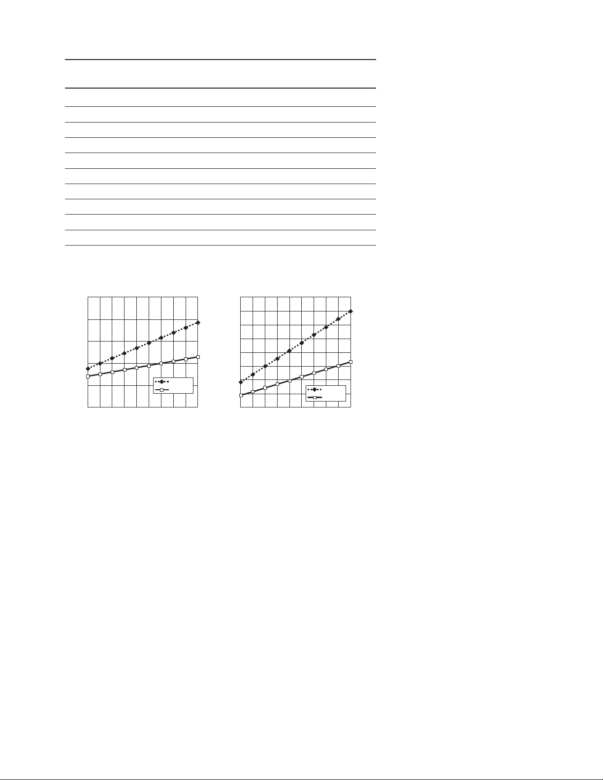
Module Depth Aperture Width (x, mm) Aperture Height (y, mm)
(z) mm Max. Min. Max. Min.
0 8.76 6.80 3.66 1.70
1 9.92 7.33 4.82 2.33
2 11.07 7.87 5.97 2.77
3 12.22 8.41 7.12 3.31
4 13.38 8.94 8.28 3.84
5 14.53 9.48 9.43 4.38
6 15.69 10.01 10.59 4.91
7 16.84 10.55 11.74 5.45
8 18.00 11.09 12.90 5.99
9 19.15 11.62 14.05 6.52
APERTURE WIDTH (X) vs. MODULE DEPTH
25
20
15
10
5
APERTURE WIDTH (X) – mm
0
09
13 5 8
MODULE DEPTH (Z) – mm
47
26
X MAX.
X MIN.
APERTURE HEIGHT (Y) vs. MODULE DEPTH
16
14
12
10
8
6
4
APERTURE HEIGHT (Y) – mm
2
0
09
13 5 8
47
26
MODULE DEPTH (Z) – mm
Y MAX.
Y MIN.
Figure 20. Aperture width (X) vs. module depth. Figure 21. Aperture height (Y) vs. module depth.
17
Page 18
Window Material
Almost any plastic material will
work as a window material.
Polycarbonate is recommended.
The surface finish of the plastic
should be smooth, without any
texture. An IR filter dye may be
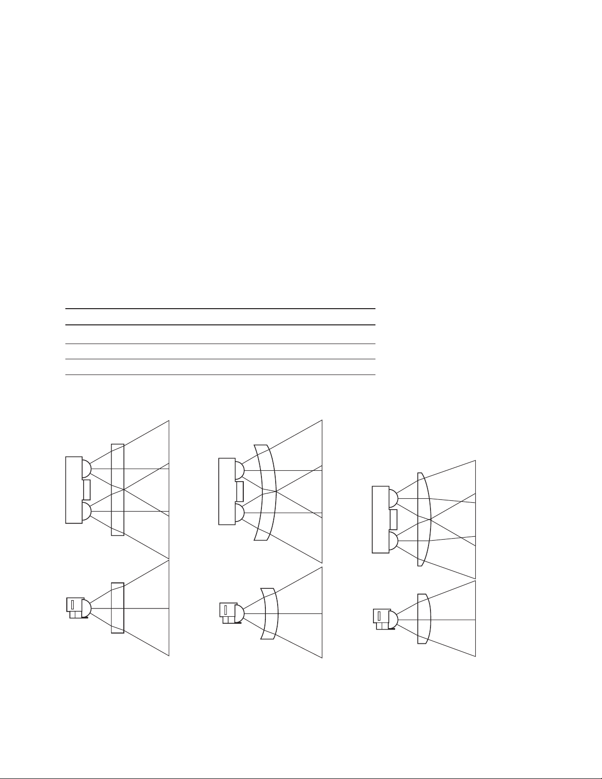
Shape of the Window
From an optics standpoint, the
window should be flat. This
ensures that the window will not
alter either the radiation pattern
of the LED, or the receive pattern
of the photodiode.
used in the window to make it
look black to the eye, but the
total optical loss of the window
should be 10% or less for best
optical performance. Light loss
should be measured at 875 nm.
The recommended plastic
materials for use as a cosmetic
window are available from
General Electric Plastics.
If the window must be curved for
mechanical or industrial design
reasons, place the same curve on
the back side of the window that
has an identical radius as the
front side. While this will not
completely eliminate the lens
effect of the front curved surface,
it will significantly reduce the
effects. The amount of change in
Recommended Plastic Materials:
Material # Light Transmission Haze Refractive Index
Lexan 141 88% 1% 1.586
Lexan 920A 85% 1% 1.586
Lexan 940A 85% 1% 1.586
Note: 920A and 940A are more flame retardant than 141.
the radiation pattern is depen-
dent upon the material chosen
for the window, the radius of the
front and back curves, and the
distance from the back surface to
the transceiver. Once these items
are known, a lens design can be
made which will eliminate the
effect of the front surface curve.
The following drawings show the
effects of a curved window on the
radiation pattern. In all cases,
the center thickness of the
window is 1.5 mm, the window is
made of polycarbonate plastic,
and the distance from the
transceiver to the back surface of
the window is 3 mm.
Flat Window
(First Choice)
Figure 22. Shape of windows.
18
Curved Front and Back
(Second Choice)
Curved Front, Flat Back
(Do Not Use)
Page 19

www.agilent.com/semiconductors
For product information and a complete list of
distributors, please go to our web site.
For technical assistance call:
Americas/Canada: +1 (800) 235-0312 or
(916) 788-6763
Europe: +49 (0) 6441 92460
China: 10800 650 0017
Hong Kong: (+65) 6756 2394
India, Australia, New Zealand: (+65) 6755 1939
Japan: (+81 3) 3335-8152(Domestic/International), or
0120-61-1280(Domestic Only)
Korea: (+65) 6755 1989
Singapore, Malaysia, Vietnam, Thailand, Philippines,
Indonesia: (+65) 6755 2044
Taiwan: (+65) 6755 1843
Data subject to change.
Copyright © 2003-2005 Agilent Technologies, Inc.
Obsoletes 5989-3140EN
August 18, 2005
5989-3640EN
 Loading...