

Page 1
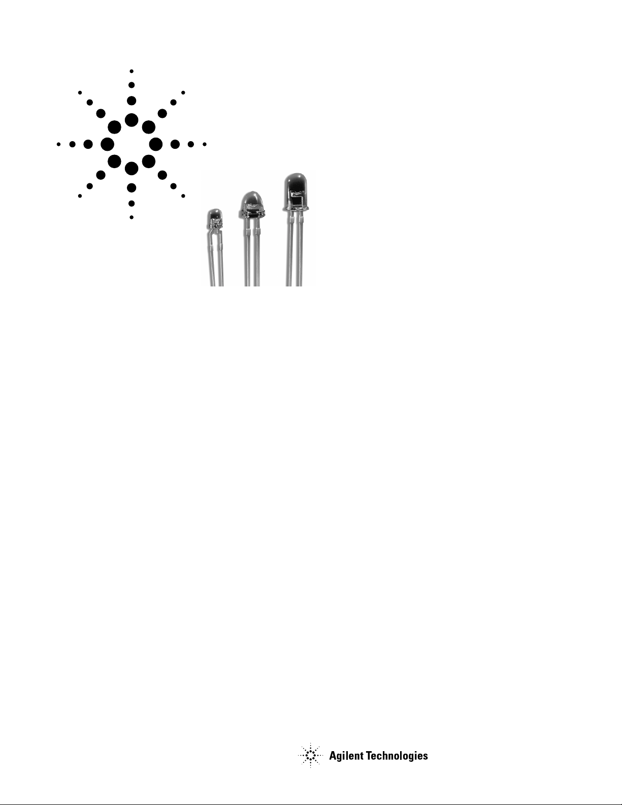
Agilent HLMP-3707
T-13/4 (5 mm), T-1 (3 mm),
Ultra-Bright LED Lamps
Data Sheet
HLMP-3707, -3807, -3907; HLMP-3750, -3850, -3950, -3960
HLMP-3390, -3490, -3590; HLMP-1340, -1440, -1540
HLMP-D640; HLMP-K640
Description
These non-diffused lamps outperform conventional LED
lamps. By utilizing new higher
intensity material, we achieve
superior product performance.
The HLMP-3750/-3390/-1340
Series Lamps are Gallium
Arsenide Phosphide on
Gallium Phosphide red light
emitting diodes. The
HLMP-3850/-3490/-1440 Series
are Gallium Arsenide Phosphide
on Gallium Phosphide yellow
light emitting diodes. The
HLMP-3950/-3590/-3960/-1540/
-D640/-K640 Series Lamps are
Gallium Phosphide green light
emitting diodes.
Features
• Improved brightness
• Improved color performance
• Available in popular T-1 and
T-13/4 packages
• New sturdy leads
• IC compatible/low current
capability
• Reliable and rugged
• Choice of 3 bright colors
High Efficiency Red
High Brightness Yellow
High Performance Green
Applications
• Lighted switches
• Backlighting front panels
• Light pipe sources
• Keyboard indicators
Page 2
Selection Guide
Luminous Intensity Iv (mcd) @ 20mA
Package Device Package
Description Color HLMP- Min. Typ. Max. 2q1/2 Degree Outline
T-13/
4
Red 3707-L00xx 90.2 - - 24 F
3750 90.2 125.0 - 24 A
3750-L00xx 90.2 125.0 - 24 A
Yellow 3807-K00xx 96.2 - - 24 F
3850 96.2 140.0 - 24 A
3850-K00xx 96.2 140.0 - 24 A
3850-KL0xx 96.2 150.0 294.0 24 A
Green 3907-K00xx 111.7 - - 24 F
3914-K00xx 111.7 - - 24 D
3950 111.7 265.0 - 24 A
3950-K00xx 111.7 265.0 - 24 A
3950-LM0xx 170.0 300.0 490.0 24 A
3960-K0xxx 111.7 265.0 - 24 E
Emerald Green D640-E00xx 6.7 21.0 - 24 D
T-13/4 Low Profile Red 3390 35.2 55.0 - 32 B
Yellow 3490 37.6 55.0 - 32 B
3490-I00xx 37.6 55.0 - 32 B
Green 3590 43.6 55.0 - 32 B
3590-I00xx 43.6 55.0 - 32 B
T-1 Red 1340 35.2 55.0 - 45 C
1340-H00xx 8.6 15.0 27.6 45 C
1340-J00xx 35.2 55.0 - 45 C
1340-JK0xx 35.2 55.0 112.8 45 C
Yellow 1440 23.5 45.0 - 45 C
1440-H00xx 23.5 45.0 - 45 C
1440-HI0xx 23.5 - 75.2 45 C
1440-HIB00 23.5 - 75.2 45 C
Green 1540 27.3 45.0 - 45 C
1540-H00xx 27.3 45.0 - 45 C
1540-IJ0xx 43.6 60.0 139.6 45 C
Emerald Green K640 4.2 21.0 - 45 C
K640-D00xx 4.2 21.0 - 45 C
K640-FGNxx 10.6 20.0 34.0 45 C
2
Page 3

Package Dimensions
25.40
MIN.
(1.00)
CATHODE
LEAD
(NOTE 1)
1.27 (0.050)
NOM.
PACKAGE OUTLINE "D"
HLMP-D640
5.08 (0.200)
4.57 (0.180)
9.19 (0.362)
8.43 (0.332)
0.89 (0.035)
0.64 (0.025)
0.102 (0.004)
MAX. TYP.
0.46 (0.018)
SQUARE
NOMINAL
6.10 (0.240)
5.59 (0.220)
2.54 (0.100)
NOM.
12.47 (0.491)
11.71 (0.461)
22.86
MIN.
(0.900)
1.52 (0.060)
1.02 (0.040)
CATHODE
FLAT
PACKAGE OUTLINE "E"
HLMP-3960
5.08 (0.200)
4.78 (0.188)
0.89 (0.035)
0.64 (0.025)
0.10 (0.004)
MAX.
0.74 (0.029)
0.58 (0.023)
SQUARE
6.10 (0.240)
∅
5.60 (0.220)
2.54 (0.100)
NOM.
9.07 (0.357)
8.56 (0.337)
1.02 (0.040)
MAX.
13.11 (0.516)
12.34 (0.486)
23.0
MIN.
(0.900)
1.52 (0.060)
1.02 (0.040)
CATHODE
FLAT
PACKAGE OUTLINE "F"
HLMP-3707/-3807/-3907
5.08 (0.200)
4.78 (0.188)
0.89 (0.035)
0.64 (0.025)
1.32 (0.052)
1.02 (0.040)
0.53 (0.021)
0.43 (0.017)
6.10 (0.240)
5.60 (0.220)
2.79 (0.110)
2.29 (0.090)
9.07 (0.357)
8.56 (0.337)
1.02 (0.040) MAX.
EPOXY
MENISCUS
SQ.
3
Page 4
Part Numbering System
HLMP - x x xx - x x x xx
Mechanical Options
00: Bulk
01: Tape & Reel, Crimped Leads
02, Bx: Tape & Reel, Straight Leads
A1, B1: Right Angle Housing, Uneven Leads
A2, B2: Right Angle Housing, Even Leads
Dx, Ex: Ammo Pack, Straight Leads
FH: 2 Iv Bin Select with Inventory Control
Vx: Ammo Pack, Crimped Leads
Color Bin Options
0: Full Color Bin Distribution
B: Color Bin 2 & 3 Only
N: Color Bin 6 & 7 Only
Maximum Iv Bin Options
0: Open (No. Max. Limit)
Others: Please Refer to the Iv Bin Table
Minimum Iv Bin Options
Please Refer to the Iv Bin Table
Color Options
3, 7: GaP HER
4, 8: GaP Yellow (except K4xx series)
5, 9: GaP Green
6: GaP Emerald Green
Package Option
1, K: T-1 (3 mm)
3, D: T-13/4 (5 mm)
Absolute Maximum Ratings at TA = 25°C
Parameter Red Yellow Green/Emerald Green Units
Peak Forward Current 90 60 90 mA
Average Forward Current
DC Current
[2]
Transient Forward Current
[1]
25 20 25 mA
30 20 30 mA
[3]
500 500 500 mA
(10 µs Pulse)
Reverse Voltage (IR = 100 µA) 5 5 5 V
LED Junction Temperature 110 110 110 °C
Operating Temperature Range -55 to +100 -55 to +100 -20 to +100 °C
Storage Temperature Range -55 to +100
Notes:
1. See Figure 2 to establish pulsed operating conditions.
2. For Red and Green series derate linearly from 50°C at 0.5 mA/°C. For Yellow series derate linearly from 50°C at 0.2 mA/°C.
3. The transient peak current is the maximum non-recurring peak current the devices can withstand without damaging the LED die and wire bonds. It
is not recommended that the device be operated at peak currents beyond the Absolute Maximum Peak Forward Current.
4
Page 5

Electrical/Optical Characteristics at T
Symbol Description T-13/
λ
PEAK
Peak 37xx 3390 1340 635 nm Measurement
= 25°C
A
T-13/
4
Low Dome T-1 Min. Typ. Max. Units Conditions
4
Test
Wavelength 38xx 3490 1440 583 at Peak
39xx 3590 1540 565
D640 K640 558
λ
d
Dominant 37xx 3390 1340 626 nm Note 1
Wavelength 38xx 3490 1440 585
39xx 3590 1540 569
D640 K640 560
∆λ3/
Spectral Line 37xx 3390 1340 40 nm
4
Halfwidth 38xx 3490 1440 36
39xx 3590 1540 28
D640 K640 24
τ
s
Speed of 37xx 3390 1340 90 ns
Respond 38xx 3490 1440 90
39xx 3590 1540 500
D640 K640 3100
C Capacitance 37xx 3390 1340 11 pF VF = 0,
38xx 3490 1440 15 f = 1 MHz
39xx 3590 1540 18
D640 K640 35
Rθ
J-PIN
Thermal 37xx 3390 210 °C/W Junction to
Resistance 38xx 3490 210 Cathode Lead
39xx 3590 210
D640 510
1340 290
1440 290
1540 290
K640 290
V
F
Forward 37xx 3390 1340 1.5 1.9 2.6 V IF = 20 mA
Voltage 38xx 3490 1440 1.5 2.1 2.6 (Figure 3)
39xx 3590 1540 1.5 2.2 3.0
D640 K640 2.2 3.0
V
R
Reverse 37xx 3390 1340 5.0 V IF = 100 µA
Breakdown 38xx 3490 1440
Voltage 39xx 3590 1540
D640 K640
η
v
Luminous 37xx 3390 1340 145 lumens Note 2
Efficacy 38xx 3490 1440 500
watt
39xx 3590 1540 595
D640 K640 655
Notes:
1. The dominant wavelength, ld, is derived from the CIE chromaticity diagram and represents the single wavelength which defines the color of the
device.
2. The radiant intensity, Ie, in watts per steradian, may be found from the equation Ie = IV/hV , where IV is the luminous intensity in candelas and hV is
the luminous efficacy in lumens/watt.
5
Page 6

Red, Yellow, and Green
1.0
EMERALD GREEN
T = 25° C
A
GREEN
0.5
YELLOW
RELATIVE INTENSITY
0
500 550 600 650 700
WAVELENGTH – nm
Figure 1. Relative intensity vs. wavelength.
HIGH EFFICIENCY RED
Figure 2. Maximum tolerable peak current vs. pulse duration. (IDC MAX
Figure 3. Forward current vs. forward voltage.
as per MAX ratings).
Figure 4. Relative luminous intensity vs. forward current. Figure 5. Relative efficiency (luminous intensity per unit current) vs.
peak current.
6
Page 7

Figure 6. Relative luminous intensity vs. angular displacement.
3
/4 lamp.
T-1
Figure 8. Relative luminous intensity vs. angular displacement.
T-1 lamp.
Figure 7. Relative luminous intensity vs. angular displacement.
T-13/4 low profile lamp.
Intensity Bin Limits
Intensity Range (mcd)
Color Bin Min. Max.
Red G 9.7 15.5
H 15.5 24.8
I 24.8 39.6
J 39.6 63.4
K 63.4 101.5
L 101.5 162.4
M 162.4 234.6
N 234.6 340.0
O 340.0 540.0
P 540.0 850.0
Q 850.0 1200.0
R 1200.0 1700.0
S 1700.0 2400.0
T 2400.0 3400.0
U 3400.0 4900.0
V 4900.0 7100.0
W 7100.0 10200.0
X 10200.0 14800.0
Y 14800.0 21400.0
Z 21400.0 30900.0
Maximum tolerance for each bin limit is ±18%.
7
Page 8

Intensity Bin Limits (continued)
Color Categories
Intensity Range (mcd)
Color Bin Min. Max.
Yellow H 26.5 42.3
I 42.3 67.7
J 67.7 108.2
K 108.2 173.2
L 173.2 250.0
M 250.0 360.0
N 360.0 510.0
O 510.0 800.0
P 800.0 1250.0
Q 1250.0 1800.0
R 1800.0 2900.0
S 2900.0 4700.0
T 4700.0 7200.0
U 7200.0 11700.0
V 11700.0 18000.0
W 18000.0 27000.0
Green/ A 1.1 1.8
Emerald B 1.8 2.9
Green C 2.9 4.7
D4.7 7.6
E 7.6 12.0
F 12.0 19.1
G 19.1 30.7
H 30.7 49.1
I 49.1 78.5
J 78.5 125.7
K 125.7 201.1
L 201.1 289.0
M 289.0 417.0
N 417.0 680.0
O 680.0 1100.0
P 1100.0 1800.0
Q 1800.0 2700.0
R 2700.0 4300.0
S 4300.0 6800.0
T 6800.0 10800.0
U 10800.0 16000.0
V 16000.0 25000.0
W 25000.0 40000.0
Lambda (nm)
Color Cat # Min. Max.
Emerald Green 9 552.5 555.5
8 555.5 558.5
7 558.5 561.5
6 561.5 564.5
Green 6 561.5 564.5
5 564.5 567.5
4 567.5 570.5
3 570.5 573.5
2 573.5 576.5
Yellow 1 582.0 584.5
3 584.5 587.0
2 587.0 589.5
4 589.5 592.0
5 592.0 593.0
Orange 1 597.0 599.5
2 599.5 602.0
3 602.0 604.5
4 604.5 607.5
5 607.5 610.5
6 610.5 613.5
7 613.5 616.5
8 616.5 619.5
Maximum tolerance for each bin limit is ±0.5 nm.
Maximum tolerance for each bin limit is ±18%.
8
Page 9

Mechanical Option Matrix
Mechanical
Option Code Definition
00 Bulk Packaging, minimum increment 500 pcs/bag
01 Tape & Reel, crimped leads, min. increment 1300 pcs/bag for T-13/4, 1800 pcs/bag for T-1
02 Tape & Reel, straight leads, min. increment 1300 pcs/bag for T-13/4, 1800 pcs/bag for T-1
A1 T-1, Right Angle Housing, uneven leads, minimum increment 500 pcs/bag
A2 T-1, Right Angle Housing, even leads, minimum increment 500 psc/bag
B1 T-13/4, Right Angle Housing, uneven leads, minimum increment 500 pcs/bag
B2 T-13/4, Right Angle Housing, even leads, minimum increment 500 psc/bag
BJ T-1, Tape & Reel, straight leads, minimum increment 2000 pcs/bag
EG Ammo Pack, straight leads in 5 K increment
FH Devices that require inventory control and 2 Iv bin select
VR Ammo Pack, crimped leads, min. increment 2 k for T-13/4 and T-1
Note:
All categories are established for classification of products. Products may not be available in all categories. Please contact your local Agilent
representative for further clarification/information.
9
Page 10

Precautions
Lead Forming
• The leads of an LED lamp may be preformed or cut to
length prior to insertion and soldering into PC board.
• If lead forming is required before soldering, care must
be taken to avoid any excessive mechanical stress
induced to LED package. Otherwise, cut the leads of
LED to length after soldering process at room
temperature. The solder joint formed will absorb the
mechanical stress of the lead cutting from traveling to
the LED chip die attach and wirebond.
• It is recommended that tooling made to precisely
form and cut the leads to length rather than rely upon
hand operation.
Soldering Conditions
• Wave soldering parameter must be set and
maintained according to recommended temperature
and dwell time in the solder wave. Customer is
advised to periodically check on the soldering profile
to ensure the soldering profile used is always
conforming to recommended soldering condition.
• If necessary, use fixture to hold the LED component
in proper orientation with respect to the PCB during
soldering process.
• Proper handling is imperative to avoid excessive
thermal stresses to LED components when heated.
Therefore, the soldered PCB must be allowed to cool
to room temperature, 25°C, before handling.
• Special attention must be given to board fabrication,
solder masking, surface plating and lead holes size
and component orientation to assure solderability.
• Care must be taken during PCB assembly and
soldering process to prevent damage to LED
component.
• The closest LED is allowed to solder on board is 1.59
mm below the body (encapsulant epoxy) for those
parts without standoff.
• Recommended soldering conditions:
Manual Solder
Wave Soldering Dipping
Pre-heat Temperature 105 °C Max. –
Pre-heat Time 30 sec Max. –
Peak Temperature 250 °C Max. 260 °C Max.
Dwell Time 3 sec Max. 5 sec Max.
250
200
150
100
TEMPERATURE – °C
50
30
01020
TURBULENT WA VE
FLUXING
PREHEAT
30 40 50
TIME – SECONDS
LAMINAR WA VE
HOT AIR KNIFE
60 70 80 90 100
CONVEYOR SPEED = 1.83 M/MIN (6 FT/MIN)
PREHEAT SETTING = 150°C (100°C PCB)
SOLDER WAVE TEMPERATURE = 245°C
AIR KNIFE AIR TEMPERATURE = 390°C
AIR KNIFE DISTANCE = 1.91 mm (0.25 IN.)
AIR KNIFE ANGLE = 40°
SOLDER: SN63; FLUX: RMA
NOTE: ALLOW FOR BOARDS TO BE
SUFFICIENTLY COOLED BEFORE EXERTING
MECHANICAL FORCE.
• Recommended PC board plated through hole sizes for
LED component leads:
LED Component Plated Through
Lead Size Diagonal Hole Diameter
0.457 x 0.457 mm 0.646 mm 0.976 to 1.078 mm
(0.018 x 0.018 inch) (0.025 inch) (0.038 to 0.042 inch)
0.508 x 0.508 mm 0.718 mm 1.049 to 1.150 mm
(0.020 x 0.020 inch) (0.028 inch) (0.041 to 0.045 inch)
Note: Refer to application note AN1027 for more
information on soldering LED components.
BOTTOM SIDE
OF PC BOARD
TOP SIDE OF
PC BOARD
Figure 8. Recommended wave soldering profile.
10
Page 11

www.agilent.com/semiconductors
For product information and a complete list of
distributors, please go to our web site.
For technical assistance call:
Americas/Canada: +1 (800) 235-0312 or
(916) 788-6763
Europe: +49 (0) 6441 92460
China: 10800 650 0017
Hong Kong: (+65) 6756 2394
India, Australia, New Zealand: (+65) 6755 1939
Japan: (+81 3) 3335-8152 (Domestic/Interna-
tional), or 0120-61-1280 (Domestic Only)
Korea: (+65) 6755 1989
Singapore, Malaysia, Vietnam, Thailand,
Philippines, Indonesia: (+65) 6755 2044
Taiwan: (+65) 6755 1843
Data subject to change.
Copyright © 2005 Agilent Technologies, Inc.
Obsoletes 5989-2810
November 12, 2005
5989-4254EN
 Loading...