

www.DataSheet4U.com
Description
This 10.16 mm (0.4 inch) LED
single digit seven segment display
uses industry standard size package
and pinout. The device is available
in either common anode or common
cathode. The choice of colors
includes High Efficiency Red
(HER), Green, AlGaAs Red, and
Yellow. The gray face displays are
suitable for indoor use.
Agilent HDSP-311x/313x
10.16 mm (0.4 inch) Single Digit General
Purpose Seven Segment Display
Data Sheet
Applications
• Suitable for indoor use
• Not recommended for industrial
Features
• Industry standard size
• Industry standard pinout
10.16 mm (0.4 inch) character height
DIP lead on 2.54 mm
• Choice of colors
High Efficiency Red (HER), Green,
AlGaAs Red, and Yellow
• Excellent appearance
Evenly lighted segments gray
package gives optimum contrast
± 50 ft. viewing angle
• Design flexibility
Common anode right hand
decimal point or common cathode
right hand decimal point
• Categorized for luminous
intensity
Green and yellow categorized for
color
application, i.e., operating
temperature requirements
exceeding +85˚C or below –25˚C
• Extreme temperature cycling not
recommended
Note:
1. For additional details, please contact your
local Agilent sales office or an authorized
distributor.
[1]
Devices
HER Green AlGaAs Red Yellow Description Package Drawing
HDSP-311E HDSP-311G HDSP-311A HDSP-311Y Common Anode Right A
Hand Decimal
HDSP-313E HDSP-313G HDSP-313A HDSP-313Y Common Cathode Right B
Hand Decimal
Part Numbering System
5082 -X X X X-X X X X X
HDSP-X X X X-X X X X X
Mechanical Options
[1]
00: No Mechanical Option
Color Bin Options
[1,2]
0: No Color Bin Limitation
Maximum Intensity Bin
[1,2]
0: No Maximum Intensity Bin Limitation
Minimum Intensity Bin
[1,2]
0: No Minimum Intensity Bin Limitation
Device Configuration/Color
[1]
A: AlGaAs Red
E: High Efficiency Red
G: Green
Y: Yellow
Device Specific Configuration
[1]
Refer to Respective Datasheet
Package
[1]
Refer to Respective Datasheet
Notes:
1. For codes not listed in the figure above, please refer to the respective datasheet or contact your nearest
Agilent representative for details.
2. Bin options refer to shippable bins for a part number. Color and Intensity Bins are typically restricted to 1
bin per tube (exceptions may apply). Please refer to respective datasheet for specific bin limit information.
2
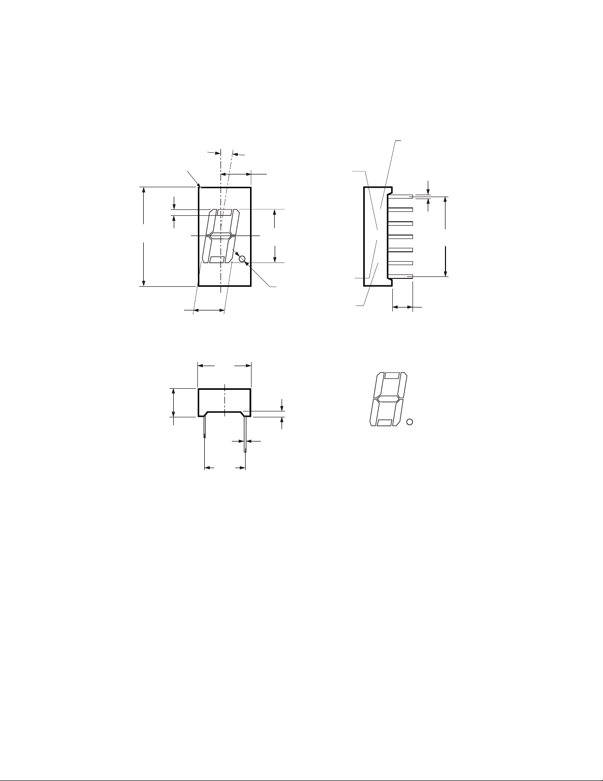
Package Dimensions
Package Drawing A
18.75
(0.738)
PIN 1
1.20
(0.047)
5.54
(0.218)
FRONT VIEW
+
SIDE VIEW
9.80
(0.386)
TOP END VIEW
COUNTRY
8°
5.51
(0.220)
10.16
(0.400)
∅1.4
(0.55)
0.60
(0.020)
COLOR
BINNING
(NOTE 3)
LUMINOUS
INTENSITY
CATEGORY
DATE CODE
F
OF ORIGIN
HDSP-XXXX
YWW XZ COO
A
B
G
0.50
(0.020)
2.54 x 6
4.10
(0.161)
(0.100)
5.10
(0.201)
7.62
(0.300)
0.30
(0.012)
E
NOTE: NO PINS 4, 5, 6, AND 12
DIMENSIONS IN MILLIMETERS (INCHES)
C
DP
D
3
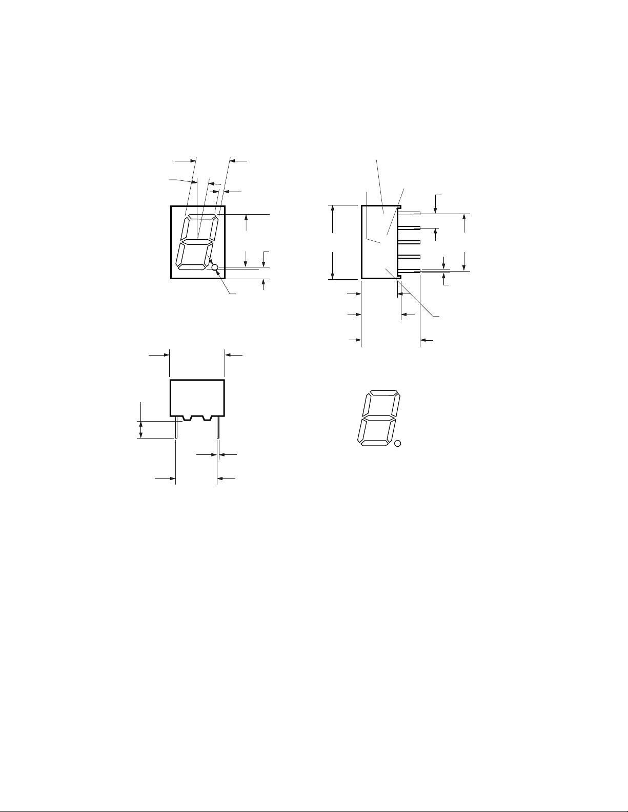
Package Dimensions
Package Drawing B
3.90
(0.153)
10.00°
FRONT VIEW
6.00
(0.236)
TOP SIDE
9.70 ± 0.25
(0.382)
7.62 ± 0.38
(0.300)
0.90
(0.035)
10.00
(0.394)
∅1.20
(0.047)
0.30 ± 0.05
(0.012)
1.85
(0.073)
RIGHT SIDE
COUNTRY
OF ORIGIN
LUMINOUS
INTENSITY
CATEGORY
12.80 ± 0.25
(0.504)
6.40 ± 0.25
(0.252)
E
DIMENSIONS IN MILLIMETERS (INCHES)
HDSP-XXXX
7.00 ± 0.25
(0.276)
10.40
(0.409)
A
F
G
D
COLOR BIN
YWW XZ COO
MIN.
B
C
DP
2.54 ± 0.38
(0.100)
4 x 2.54
(0.400)
0.50 ± 0.05
(0.02)
DATE
CODE
4

Internal Circuit Diagram
ABCDEFGDP
11310872119
COMMON ANODE RIGHT HAND DECIMAL
3.14 COM
HDSP-311E/311G/311Y/311A
PIN No.
1
2
3
7
8
9
10
11
13
14
PINS 4, 5, 6, 12: NO PIN
CONNECTION
CATHODE A
CATHODE F
COMMON ANODE
CATHODE E
CATHODE D
CATHODE DP
CATHODE C
CATHODE G
CATHODE B
COMMON ANODE
COMMON CATHODE RIGHT HAND DECIMAL
3.8 COM
ABCDEFGDP
10 9 7
5
4216
HDSP-313E/313G/313Y/313A
PIN NO.
1
2
3
4
5
6
7
8
9
10
CONNECTION
ANODE G
ANODE F
COMMON CATHODE
ANODE E
ANODE D
ANODE DP
ANODE C
COMMON CATHODE
ANODE B
ANODE A
5

Absolute Maximum Ratings at TA = 25˚C
HER Green AlGaAs Red Yellow
Description HDSP-31xE HDSP-31xG HDSP-31xA HDSP-31xY Units
Power Dissipation Segment 65 65 30 52 mW
Forward Current Segment 25
[1]
25
[2]
15
[3]
20
[4]
mA
Peak Forward Current per Segment 100 100 80 80 mA
(1/10 Duty Factor at 10 KHz)
Operating Temperature Range –35 to +85 –35 to +85 –35 to +85 –35 to +85 ˚C
Storage Temperature Range –35 to +85 –35 to +85 –35 to +85 –35 to +85 ˚C
Reverse Voltage per Segment or DP 5 5 5 5 V
Wavesoldering Temperature for 3 seconds 250 250 250 250 ˚C
(at 2 mm Distance from the body)
Notes:
1. Derate above 25˚C at 0.33 mA/˚C.
2. Derate above 25˚C at 0.33 mA/˚C.
3. Derate above 25˚C at 0.2 mA/˚C.
4. Derate above 25˚C at 0.27 mA/˚C.
Electrical/Optical Characteristics at TA = 25˚C
High Efficiency Red (HER)
Devices
HDSP- Parameter Symbol Min. Typ. Max. Units Test Conditions
Luminous Intensity/Segment I
V
1.49 mcd IF = 5 mA
1.25 3.20 mcd IF = 10 mA
311E
313E
Forward Voltage V
Peak Wavelength λ
Dominant Wavelength λ
F
PEAK
d
2.05 2.40 V IF = 20 mA
635 nm
620 nm
Reverse Voltage VR 5 V IR = 100 µA
Green
Devices
HDSP- Parameter Symbol Min. Typ. Max. Units Test Conditions
311G
313G
Luminous Intensity/Segment I
Forward Voltage V
Peak Wavelength λ
Dominant Wavelength λ
V
F
PEAK
d
1.25 3.20 mcd IF = 10 mA
2.06 V IF = 10 mA
1.80 2.25 2.60 V IF = 20 mA
568 nm
573 nm
Reverse Voltage VR 5 V IR = 100 µA
6

AlGaAs Red
Devices
HDSP- Parameter Symbol Min. Typ. Max. Units Test Conditions
Luminous Intensity/Segment I
V
4.54 mcd IF = 5 mA
3.20 7.50 mcd IF = 10 mA
311A
313A
Forward Voltage V
Peak Wavelength λ
Dominant Wavelength λ
F
PEAK
d
1.85 2.00 V IF = 20 mA
660 nm
643 nm
Reverse Voltage VR 5 V IR = 100 µA
Yellow
Devices
HDSP- Parameter Symbol Min. Typ. Max. Units Test Conditions
Luminous Intensity/Segment I
V
0.86 mcd IF = 5 mA
0.80 1.50 mcd IF = 10 mA
311Y
313Y
Forward Voltage V
Peak Wavelength λ
Dominant Wavelength λ
F
PEAK
d
2.15 2.60 V IF = 20 mA
595 nm
590 nm
Reverse Voltage VR 5 V IR = 100 µA
Intensity Bin Limits (mcd at 10 mA)
Bin HER/Green Yellow AlGaAs Red
Name Min.
[1]
Max.
[1]
Min.
[1]
Max.
[1]
Min.
[1]
Max.
G NA NA 0.801 1.250 NA NA
H 1.251 2.000 1.251 2.000 NA NA
I 2.001 3.200 2.001 3.200 NA NA
J 3.201 5.050 NA NA 3.201 5.050
K NA NA NA NA 5.051 8.000
L NA NA NA NA 8.001 12.650
Note:
1. Tolerance for each bin limit is ± 10%.
Color Bin Limits (nm at 10 mA)
Dominant Wavelength (nm)
Color Bin Min.
[1]
Max.
[1]
Green 3 569.1 571.0
4 571.1 573.0
5 573.1 575.0
Yellow 1 585.5 588.5
2 588.5 591.5
3 591.5 594.5
Note:
1. Tolerance for each bin limit is 1 nm.
[1]
7

High Efficiency Red (HER)
30
HIGH EFFICIENCY RED (HER)
25
20
15
10
5
0
0 20 40 60 80 100
MAXIMUM DC CURRENT PER SEGMENT – mA
T
– AMBIENT TEMPERATURE – °C
A
Figure 1. Maximum allowable average or DC
current vs. ambient temperature.
2.5
2.0
1.5
1.0
0.5
(NORMALIZED TO 1 AT 10 mA)
RELATIVE LUMINOUS INTENSITY
0
0 5 10 15 20 25 30
– FORWARD CURRENT FOR SEGMENT – mA
I
F
120
100
80
60
40
20
0
0 0.5 1.0 1.5 2.0 2.5 3.0 3.5
– FORWARD CURRENT PER SEGMENT – mA
F
I
VF – FORWARD VOLTAGE – V
Figure 2. Forward current vs. forward voltage.
1.4
1.2
1.0
0.8
0.6
0.4
RELATIVE EFFICIENCY
0.2
(NORMALIZED TO 1 AT 10 mA)
0
35
0 5 10 15 20 25 30 35 40 45 50
– PEAK FORWARD CURRENT
I
PEAK
PER SEGMENT – mA
Figure 3. Relative luminous intensity vs. DC
forward current.
8
Figure 4. Relative efficiency (luminous
intensity per unit current) vs. peak current.

Green
30
GAP GREEN
25
20
15
10
5
0
0 20 40 60 80 100
MAXIMUM DC CURRENT PER SEGMENT – mA
– AMBIENT TEMPERATURE – °C
T
A
Figure 5. Maximum allowable average or DC
current vs. ambient temperature.
3.0
2.5
2.0
1.5
120
100
80
60
40
20
0
0 0.5 1.0 1.5 2.0 2.5 3.0 3.5
– FORWARD CURRENT PER SEGMENT – mA
F
I
VF – FORWARD VOLTAGE – V
Figure 6. Forward current vs. forward
voltage.
1.2
1.0
0.8
0.6
1.0
0.5
(NORMALIZEDTO 1 AT 10 mA)
RELATIVE LUMINOUS INTENSITY
0
0 5 10 15 20 25 30
I
– FORWARD CURRENT FOR SEGMENT – mA
F
Figure 7. Relative luminous intensity vs. DC
forward current.
0.4
RELATIVE EFFICIENCY
0.2
(NORMALIZED TO 1 AT 10 mA)
35
0
0 5 10 15 20 25 30 35 40 45 50
– PEAK FORWARD CURRENT
I
PEAK
PER SEGMENT – mA
Figure 8. Relative efficiency (luminous
intensity per unit current) vs. peak current.
9

AlGaAs Red
16
14
12
10
8
6
4
2
0
0 20 40 60 80 100
MAXIMUM DC CURRENT PER SEGMENT – mA
T
A
AIGaAs RED
– AMBIENT TEMPERATURE – °C
Figure 9. Maximum allowable average or DC
current vs. ambient temperature.
3.0
2.5
2.0
1.5
120
100
80
60
40
20
0
0 0.5 1.0 1.5 2.0 2.5
– FORWARD CURRENT PER SEGMENT – mA
F
I
VF – FORWARD VOLTAGE – V
Figure 10. Forward current vs. forward voltage.
1.2
1.0
0.8
0.6
1.0
0.5
(NORMALIZED TO 1 AT 10 mA)
RELATIVE LUMINOUS INTENSITY
0
0 5 10 15 20 25 30
I
– FORWARD CURRENT FOR SEGMENT – mA
F
Figure 11. Relative luminous intensity vs. DC
forward current.
0.4
RELATIVE EFFICIENCY
0.2
(NORMALIZED TO 1 AT 10 mA)
35
0
0 5 10 15 20 25 30 35 40 45 50
– PEAK FORWARD CURRENT
I
PEAK
PER SEGMENT – mA
Figure 12. Relative efficiency (luminous
intensity per unit current) vs. peak current.
10

Yellow
25
YELLOW
20
15
10
5
0
0 20 40 60 80 100
MAXIMUM DC CURRENT PER SEGMENT – mA
– AMBIENT TEMPERATURE – °C
T
A
Figure 13. Maximum allowable average or
DC current vs. ambient temperature.
3.5
3.0
2.5
2.0
1.5
1.0
0.5
(NORMALIZEDTO 1 AT 10 mA)
RELATIVE LUMINOUS INTENSITY
0
0 5 10 15 20 25 30
I
– FORWARD CURRENT FOR SEGMENT – mA
F
120
100
80
60
40
20
0
0 0.5 1.0 1.5 2.0 2.5 3.0 3.5
– FORWARD CURRENT PER SEGMENT – mA
F
I
VF – FORWARD VOLTAGE – V
Figure 14. Forward current vs. forward voltage.
1.4
1.2
1.0
0.8
0.6
0.4
RELATIVE EFFICIENCY
0.2
(NORMALIZED TO 1 AT 10 mA)
0
35
0 5 10 15 20 25 30 35 40 45 50
I
– PEAK FORWARD CURRENT
PEAK
PER SEGMENT – mA
Figure 15. Relative luminous intensity vs. DC
forward current.
11
Figure 16. Relative efficiency (luminous
intensity per unit current) vs. peak current.

www.agilent.com/semiconductors
For product information and a complete list of
distributors, please go to our web site.
For technical assistance call:
Americas/Canada: +1 (800) 235-0312 or
(916) 788-6763
Europe: +49 (0) 6441 92460
China: 10800 650 0017
Hong Kong: (+65) 6756 2394
India, Australia, New Zealand: (+65) 6755 1939
Japan: (+81 3) 3335-8152(Domestic/
International), or 0120-61-1280(Domestic Only)
Korea: (+65) 6755 1989
Singapore, Malaysia, Vietnam, Thailand,
Philippines, Indonesia: (+65) 6755 2044
Taiwan: (+65) 6755 1843
Data subject to change.
June 30, 2004
5988-2969EN
 Loading...