

Page 1
www.DataSheet4U.com
Glass/Ceramic Numeric and
Hexadecimal Displays for
Industrial Applications
Technical Data
Features
• Three Character Options
Numeric, Hexadecimal, Over
Range
• Three Colors
High Efficiency Red, Yellow,
High Performance Green
• 4 x 7 Dot Matrix Character
• High Efficiency Red, Yellow
and High Performance Green
• Two High Efficiency Red
Options
Low Power, High Brightness
• Performance Guaranteed
Over Temperature
• High Temperature Stabilized
• Memory Latch/Decoder/
Driver
TTL Compatible
• Categorized for Luminous
Intensity
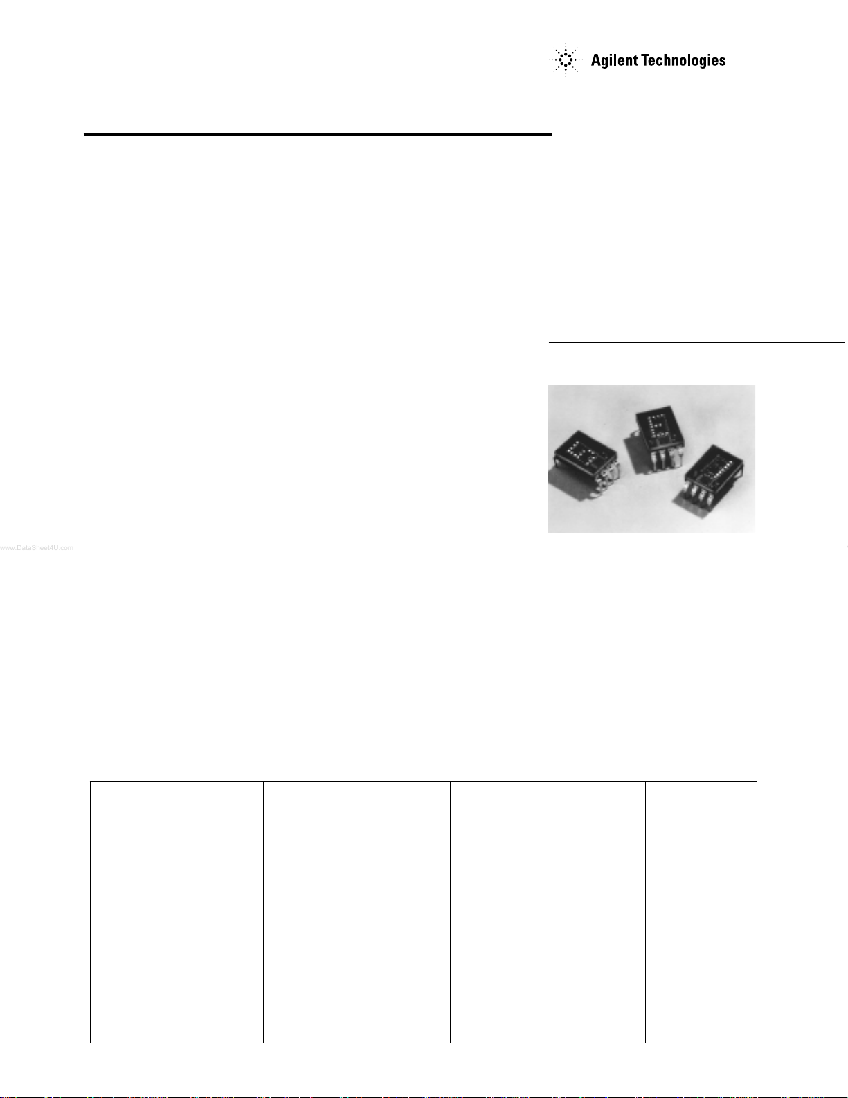
Description
These standard solid state displays
have a 7.4 mm (0.29 inch) dot
matrix character and an on-board
IC with data memory latch/
decoder and LED drivers in a
glass/ceramic package.
The hermetic HDSP-078x,-079x/
-088x displays utilize a solder
glass frit seal. The HDSP-098X
displays utilize an epoxy glass-toceramic seal.
The numeric devices decode positive BCD logic into characters
“0-9,” a “–” sign, decimal point,
and a test pattern. The
hexadecimal devices decode
HDSP-078x
HDSP-079x
HDSP-088x
HDSP-098x
positive BCD logic into 16
characters, “0-9, A-F.” An input is
provided on the hexadecimal
devices to blank the display (all
LEDS off) without losing the
contents of the memory.
The over range device displays
“±1” and right hand decimal
point and is typically driven via
external switching transistors.
Devices
Part Number HDSP- Color Description Front View
0781 High-Efficiency Red Numeric, Right Hand DP A
0782 Low Power Numeric, Left Hand DP B
0783 Over Range ± 1C
0784 Hexadecimal D
0791 High-Efficiency Red Numeric, Right Hand DP A
0792 High Brightness Numeric, Left Hand DP B
0793 Over Range ± 1C
0794 Hexadecimal D
0881 Yellow Numeric, Right Hand DP A
0882 Numeric, Left Hand DP B
0883 Over Range ± 1C
0884 Hexadecimal D
0981 High-Performance Green Numeric, Right Hand DP A
0982 Numeric, Left Hand DP B
0983 Over Range ± 1C
0984 Hexadecimal D
Page 2
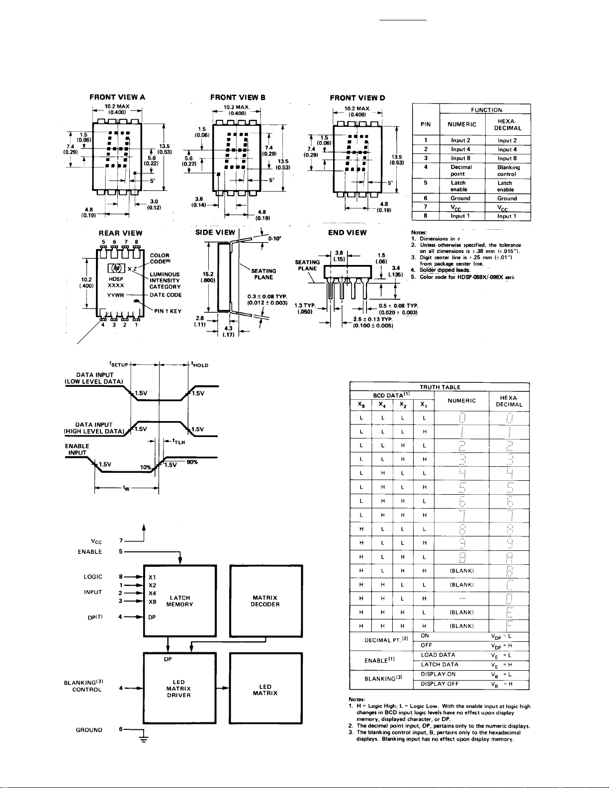
Package Dimensions
SYYWW
2
COUNTRY CODE
Figure 1. Timing Diagram.
Figure 2. Block Diagram.
Page 3
3
Absolute Maximum Ratings
Description Symbol Min. Max. Unit
Storage Temperature, Ambient
HDSP-078x/-079x/-088x T
S
-65 +125 °C
HDSP-098x -55 +100
Operating Temperature, Ambient
Supply Voltage
[2]
Voltage Applied to Input Logic, dp and Enable Pins VI, VDP, V
Voltage Applied to Blanking Input
[1]
[2]
T
A
V
CC
E
V
R
-55 +100 °C
-0.5 +7.0 V
-0.5 V
-0.5 V
CC
CC
Wave Solder Temperature at 1.59 mm (0.063 inch) 250 °C
below Body, max. 3 seconds
Recommended Operating Conditions
Description Symbol Min. Nom. Max. Unit
Supply Voltage
Operating Temperature, Ambient
Enable Pulse Width t
Time Data Must Be Held Before Positive t
Transition of Enable Line
Time Data Must Be Held After Positive t
Transition of Enable Line
Enable Pulse Rise Time t
[2]
[1]
V
CC
T
A
W
SETUP
HOLD
TLH
4.5 5.0 5.5 V
–55 +100 °C
100 nsec
50 nsec
50 nsec
1.0 msec
V
V
Optical Characterstics at T
= 25°C, V
A
= 5.0 V
CC
Device Description Symbol Min. Typ. Max. Unit
HDSP-078x Series Luminous Intensity per LED I
(Digit Average)
[3,4]
Peak Wavelength λ
Dominant Wavelength
[5]
HDSP-079x Series Luminous Intensity per LED I
(Digit Average)
[3,4]
Peak Wavelength λ
Dominant Wavelength
[5]
HDSP-088x Series Luminous Intensity per LED I
(Digit Average)
[3,4]
Peak Wavelength λ
Dominant Wavelength
[5,6]
HDSP-098x Series Luminous Intensity per LED I
(Digit Average)
[3,4]
Peak Wavelength λ
Dominant Wavelength λ
Notes:
1. The nominal thermal resistance of a display mounted in a socket that is soldered onto a printed circuit board is
RθJA=50°C/W/device. The device package thermal resistance is Rθ
ambient through the PC board should not exceed 35°C/W/device for operation up to TA = +100°C.
2. Voltage values are with respect to device ground, pin 6.
3. These displays are categorized for luminous intensity with the intensity category designated by a letter code located on the back of
the display package. Case temperature of the device immediately prior to the light measurement is equal to 25°C.
V
PEAK
λ
d
V
PEAK
λ
d
V
PEAK
λ
d
V
PEAK
d
= 15°C/W/device. The thermal resistance device pin-to-
J-PIN
65 140 µcd
635 nm
626 nm
260 620 µcd
635 nm
626 nm
215 490 µcd
583 nm
585 nm
298 1100 µcd
568 nm
574 nm
Page 4

4
Electrical/Optical Characteristics
T
= –55°C to +100°C
A
Description Symbol Test Conditions Min. Typ.
Supply HDSP-078x Series I
CC
VCC = 5.5 V 78 105 mA
Current HDSP-079x/-088x/ Characters “5.” or
-098x Series “B” displayed
Power HDSP-078x Series P
T
VCC = 5.5 V 390 573 mW
Dissipation HDSP-079x/-088x/ Characters “5.” or
-098x Series “B” displayed
Logic, Enable and Blanking V
IL
VCC = 4.5 V 0.8 V
Low-Level Input Voltage
Logic, Enable High-Level Input V
IH
2.0 V
Voltage
Blanking High-Voltage; Display V
BH
2.3 V
Blanked
Logic and Enable Low-Level I
IL
VCC = 5.5 V –1.6 mA
Input Current
Blanking Low-Level Input Current I
Logic, Enable and Blanking I
BL
IH
V
= 0.4 V –10 µA
IL
V
= 5.5 V +40 µA
CC
High-Level Input Current VIH = 2.4 V
Weight 1.0 gm
Leak Rate 5 x 10
[7]
Max. Unit
120 175
690 963
-8
cc/sec
Notes:
4. The luminous intensity at a specific operating ambient
temperature, Iv(TA), may be approximated from the following
exponential equation: Iv(TA)=I
Device K
HDSP-078 Series –0.0131/°C
HDSP-079x Series
HDSP-088x Series – 0.0112/ °C
HDSP-098x Series – 0.0104/ °C
v
Operational
Considerations
Electrical
These devices use a modified
4 x 7 dot matrix of light emitting
diodes to display decimal/
hexadecimal numeric information. The high efficiency red and
(25°C) e
[k(T -25°C)]
A
.
line is at logic low and the data is
latched when the enable is at
logic high. Using the enable pulse
width and data setup and hold
times listed in the Recommended
Operating Conditions allows data
to be clocked into an array of
displays at a 6.7 MHz rate.
yellow displays use GaAsP/GaP
LEDs and the high performance
green displays use GaP/GaP
LEDs. The LEDs are driven by
constant current drivers, BCD
information is accepted by the
display memory when the enable
The decimal point input is active
low true and this data is latched
into the display memory in the
same fashion as the BCD data.
The decimal point LED is driven
by the on-board IC.
5. The dominant wavelength, λ
ticity diagram and represents the single wavelength which
defines the color of the device.
6. The HDSP-088X and HDSP-098X series devices are categorized as to dominant wavelength with the category designated
by a number on the back of the display package.
7. All typical values at VCC = 5.0 V and T
, is derived from the CIE chroma-
d
= 25°C.
A
The blanking control input on the
hexadecimal displays blanks
(turns off) the displayed
information without disturbing
the contents of display memory.
The display is blanked at a
minimum threshold level of 2.0
volts. When blanked, the display
standby power is nominally 250
mW at T
= 25°C.
A
The ESD susceptibility of the IC
devices is Class A of MIL-STD883 or Class 2 of DOD-STD-1686
and DOD-HDBK-263.
Page 5

5
Mechanical
These displays are hermetically
sealed for use in environments
that require a high reliability
device. These displays are
designed and tested to meet a
helium leak rate of
5x10⁻⁸cc/sec.
These displays may be mounted
by soldering directly to a printed
circuit board or insertion into a
socket. The lead-to-lead pin
spacing is 2.54 mm (0.100 inch)
and the lead row spacing is 15.24
mm (0.600 inch). These displays
may be end stacked with 2.54
mm (0.100 inch) spacing
between outside pins of adjacent
displays. Sockets such as Augat
324-AG2D (3 digits) or Augat
Absolute Maximum Ratings
Description Symbol Min Max Unit
Storage Temperature, Ambient T
Operating Temperature, Ambient T
Forward Current, Each LED I
Reverse Voltage, Each LED V
508-AG8D (one digit, right angle
mounting) may be used.
The primary thermal path for
power dissipation is through the
device leads. Therefore, to insure
reliable operation up to an
ambient temperature of +100°C,
it is important to maintain a
base-to-ambient thermal
resistance of less than
35°C watt/device as measured on
top of display pin 3.
For further information on
soldering and post solder
cleaning, see Application Note
1027, Soldering LED
Components.
S
A
F
R
–65 +125 °C
–55 +100 °C
10 mA
5V
Preconditioning
These displays are 100% preconditioned by 24 hour storage at
125°C, at 100°C for the HDSP-
098x Series.
Contrast Enhancement
These display devices are
designed to provide an optimum
ON/OFF contrast when placed
behind an appropriate contrast
enhancement filter. For further
information on contrast
enhancement, see Application
Note 1015, Contrast
Enhancement for LED
Displays.
Over Range Display
The over range devices display
“±1” and decimal point. The
character height and package
configuration are the same as the
numeric and hexadecimal
devices. Character selection is
obtained via external switching
transistors and current limiting
resistors.
Page 6

Package Dimensions
6
Pin
Character 1 2,3 4 8
+1XX1
–0XX1
1X1XX
Decimal Point X X 1 X
Blank 0 0 0 0
Notes:
0: Line switching transistor in Figure 7 cutoff.
1: Line switching transistor in Figure 7 saturated.
X: ‘don’t care.’
Figure 3. Typical Driving Circuit.
Luminous Intensity per LED
(Digit Average) at T
Device Test Conditions Min. Typ. Units
HDSP-0783 I
HDSP-0883 I
HDSP-0983 I
= 25°C
A
= 2.8 mA 65 140 µcd
F
I
= 8 mA 620 µcd
F
= 8 mA 215 490 µcd
F
= 8 mA 298 1100 µcd
F
Recommended Operating Conditions
VCC = 5.0 V
Forward Resistor Value
Current Per
Device LED, mA R
HDSP-0783 Low Power 2.8 1300 200 300
High Brightness 8 360 47 68
HDSP-0883 8 360 36 56
HDSP-0983 8 360 30 43
R
1
2
R
3
Page 7

7
Electrical Characteristics
T
= –55°C to +100°C
A
Device Description Symbol Test Conditions Min Typ Max Unit
HDSP-0783 Power Dissipation P
(All LEDs Illuminated)
Forward Voltage per LED V
IF = 2.8 mA 72 mW
T
IF = 8 mA 224 282
IF = 2.8 mA 1.6 V
F
IF = 8 mA 1.75 2.2
HDSP-0883 Power Dissipation P
IF = 8 mA 237 282 mW
T
(All LEDs Illuminated)
Forward Voltage per LED V
HDSP-0883 Power Dissipation P
F
IF = 8 mA 243 282 mW
T
1.90 2.2 V
(All LEDs Illuminated)
Forward Voltage per LED V
F
1.85 2.2 V
Intensity Bin Limits for HDSP-078x Series
Bin Category Min. (mcd) Max. (mcd) Condition
A 0.065 0.102
B 0.085 0.138
C 0.114 0.200
D 0.165 0.300
E 0.260 0.488
F 0.403 0.756
G 0.625 1.172
Luminous
Intensity
per LED.
VDD @ 5.0 V
Intensity Bin Limits for HDSP-079x Series
Bin Category Min. (mcd) Max. (mcd) Condition
E 0.260 0.488
F 0.403 0.756
G 0.625 1.172
H 0.969 1.820
Luminous
Intensity
per LED.
VDD @ 5.0 V
Intensity Bin Limits for HDSP-088x Series
Bin Category Min. (mcd) Max. (mcd) Condition
A 0.22 0.34
B 0.28 0.46
C 0.38 0.66
D 0.55 0.99
E 0.82 1.54
Luminous
Intensity
per LED.
VDD @ 5.0 V
F 1.27 2.39
Intensity Bin Limits for HDSP-098x Series
Bin Category Min. (mcd) Max. (mcd) Condition
C 0.30 0.52
D 0.43 0.79
E 0.65 1.18
F 0.97 1.76
G 1.45 2.63
Luminous
Intensity
per LED.
VDD @ 5.0 V
Page 8

Color Bin Limits (Dominant Wavelength)
Intensity Range (nm)
Color Bin Min. Max.
Yellow 1 581.50 585.00
2 584.00 587.50
3 586.50 590.00
Green 1 570.00 574.00
2 573.00 577.00
3 576.00 580.00
Note:
Bin categories are established for classification of products. Products
may not be available in all bin categories. Please consult your local
Agilent Technologies representative.
www.agilent.com/semiconductors
For product information and a complete list of
distributors, please go to our web site.
For technical assistance call:
Americas/Canada: +1 (800) 235-0312 or
(916) 788-6763
Europe: +49 (0) 6441 92460
China: 10800 650 0017
Hong Kong: (+65) 6756 2394
India, Australia, New Zealand: (+65) 6755 1939
Japan: (+81 3) 3335-8152 (Domestic/International), or 0120-61-1280 (Domestic Only)
Korea: (+65) 6755 1989
Singapore, Malaysia, Vietnam, Thailand,
Philippines, Indonesia: (+65) 6755 2044
Taiwan: (+65) 6755 1843
Data subject to change.
Copyright © 2004 Agilent Technologies, Inc.
Obsoletes 5964-6390E
July 14, 2004
5988-2261EN
 Loading...