

Description
Agilent Color Sensor is a high
performance, small in size, cost
effective light to voltage
converting sensor. The sensor
combines a photodiode array
and three trans-impedance
amplifiers in a single monolithic
CMOS IC solution. With Red (R),
Green (G), and Blue (B) color
filters coated over the
photodiode array, the sensor
converts RGB light to analog
voltage outputs, denoted by
VR
, VG
OUT
respectively. The sensor is
driven by a single 5 V supply and
incorporates an internal 5 V to
3.3 V voltage regulator. The color
sensor module consists of a
color sensor packaged in a
5 x 5 x 2 [mm] surface mount
QFN-16, flat flexible cable
connector and a decoupling
capacitor mounted on a PCB.
OUT
and VB
OUT
,
Agilent HDJD-S831-QT333
Color Sensor Module
Data Sheet
Features
• Converts light to R,G,B voltage
output
• Monolithic CMOS IC solution with
integrated R,G,B color filter,
photodiode array, transimpedance amplifier in one chip
Applications
Agilent Color Sensor is ideal for
open-loop color identification
and closed-loop color point
control. The spectral sensitivity
response of the sensor is
optimized for RGB-LED
backlight applications. The
sensor has good detection ability
in light output chromaticity
drift, when used with closedloop feedback controller,
manages to bring the backlight
system to realize good du’v’
performance. Potential
applications include white point
control in emissive display,
environmental lighting, color
control in industrial processes,
and many more.
• 12x12 photodiode array design
minimizes the effect of
contamination and optical
aperture misalignment
• Spectral sensitivity response
optimized for RGB-LED backlight
application: good detection
capability in light chromaticity
drift
• Small module size
(27.6 mm x 7 mm x 3 mm)
• Internal 5 V to 3.3 V voltage
regulator
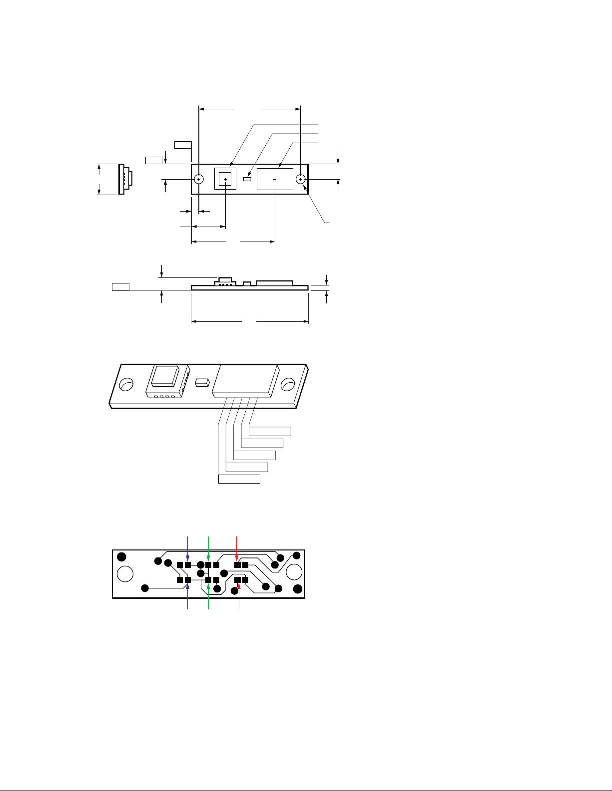
Package Dimensions
7.0
– A –
3.25 ± 0.3
24.0 ± 0.2
COLOR SENSOR
CAPACITOR
– B –
1.8
8.0
19.7
CONNECTOR
3.5
2 – ∅ 2.25 ± 0.2
– C –
NOTE: DIMENSIONS ARE IN MILLIMETERS (mm)
3.0
PIN 4 – VG
PIN 5 – VR
B0B1G0
27.6
PIN 1 – V
PIN 2 – GND
PIN 3 – VB
OUT
R0
OUT
OUT
1.0
FLAT FLEXIBLE CABLE TO BE USED
WITH THE CONNECTOR.
RECOMMENDED DIMENSIONS:
CABLE WIDTH: 3.0 ± 0.1 mm
DD
CONDUCTOR PITCH: 0.5 ± 0.1 mm
INSERT THICKNESS: 0.3 ± 0.03 mm
NOTE:
BACK VIEW OF PCB
SHORT THE 2 PADS WITH JUMPER FOR 0; LEAVE THE 2 PADS OPEN FOR 1.
DEFAULT GAIN SELECTIONS ARE GS:11 FOR RED, GREEN AND BLUE.
REFER TO GAIN SELECTION FEEDBACK RESISTOR TABLE ON PAGE 8.
G1
R1
2
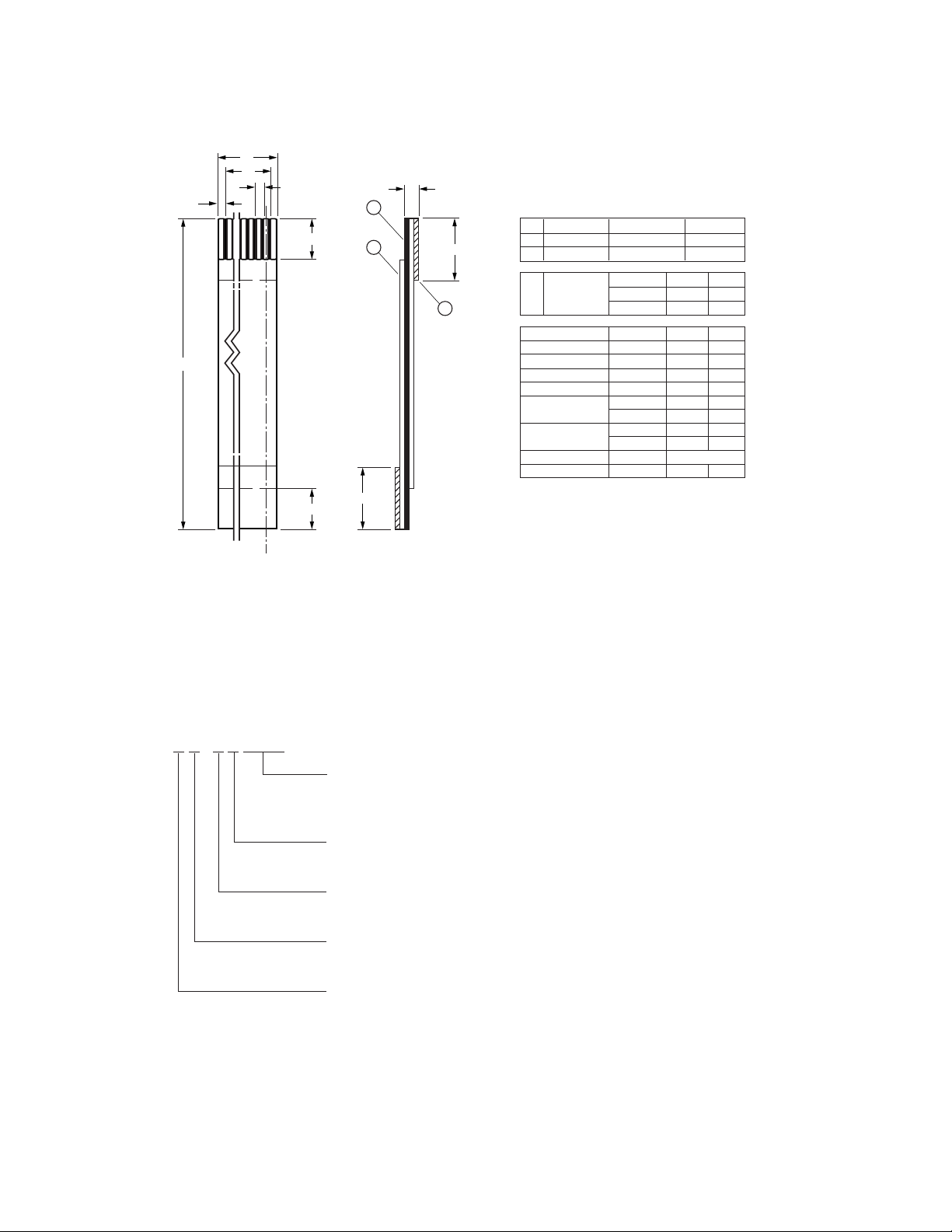
Recommended Flat Flexible Cable to be used with the Connector
W
SP
P
M
T.L
A
S1
T
3
1
B1
2
ITEM NAME
NO.
INSULATION
1
P/TAPE
2
CONDUCTOR
3
PITCH
SPAN
WIDTH
MARGIN
INSERT THICKNESS
PROTECTOR
LENGTH
STRIP
LENGTH
TOTAL LENGTH
NO. OF PIN
SPECIFICATION
20696(42 µ)
223 µ
THICKNESS
WIDTH
PLATED
P
SP
W
M
T
B1
B2
S1
S2
OPTIONAL
T.L
0.035
0.32
TIN (1 µ)
0.5
2.0
3.0
0.5
0.3
6.0
6.0
4.0
4.0
5P
REMARK
± 0.1
± 0.03
MIN.
± 0.1
± 0.1
± 0.1
± 0.1
± 0.03
± 1.5
± 1.5
± 1.0
± 1.0
A
NOTE: DIMENSIONS ARE IN MILLIMETERS (mm)
Part Numbering System
HDJD-S 8 X X - X X X X X
S2
B2
SECTION A-A
Gain Selection (GS) Option
Red Green Blue GS
333: 11 11 11
Packaging Type
T: Tray Standard Pack
Product Packaging
Q: QFN
Config ID/Filter Attachment
1: With IR Filter
Product Type
3: Module Level
3

Pin Out for HDJD-S831-QT333 Color Sensor Module
Pin Descriptions for Flat Flexible Cable Connector
Pin Name Description
1 VDD5 5 V DC Supply
2 GND Ground
3VB
4VG
5VR
OUT
OUT
OUT
Analog Output Voltage for Blue
Analog Output Voltage for Green
Analog Output Voltage for Red
Device Selection Guide
Gain Selection
[2]
Red Green Blue
Part Number GS: Bit 1 Bit 0 GS: Bit 1 Bit 0 GS: Bit 1 Bit 0
HDJD-S831-QT333
Note:
1. HDJD-S831-QT333 a is gain selections selectable. Please refer to gain Selection Feedback
Resistor Table for different feedback resistor setting for different gain selections.
2. 0 indicates that the pin is connected to ground. 1 indicates no connection.
[1]
111111
Theory of Operation
The integral R,G,B color filters
on the photodiode array detect
the R,G,B components of the
light falling on the sensor. The
photodiode converts the R,G,B
light components into
photocurrents. The integrated
transimpedence amplifiers for
R,G,B components then convert
the photocurrent to analog
voltage outputs. The voltage
output of each R,G,B channel
increases linearly with
increasing light intensity.
4

Sensor IC Block Diagram
VDD5
VOLTAGE
REGULATOR
GS (1:0)
R
F
C
F
GND
VDD3
GSRED (0:1)
GSGRN (0:1)
GSBLUE (0:1)
GREEN GAIN
Absolute Maximum Ratings
RED GAIN
SELECTION
SELECTION
BLUE GAIN
SELECTION
[1,2]
–
+
TRANSIMPEDANCE AMP
GS (1:0)
R
F
C
F
–
+
TRANSIMPEDANCE AMP
GS (1:0)
R
F
C
F
–
+
TRANSIMPEDANCE AMP
VR
OUT
VG
OUT
VB
OUT
Parameter Symbol Min. Max. Unit Notes
Supply Voltage V
Storage Temperature T
Operating Temperature T
Human Body Model ESD Rating ESD
DD5
S
A
HBM
Notes:
1. Subjecting the part to stresses beyond those listed under this section may cause permanent damage to the device. These are stress ratings only and
do not imply that the devices will function beyond these ratings. Exposure to the extremes of these conditions for extended periods may affect
device reliability.
2. Unless otherwise specified, voltages are referenced to ground.
4.5 5.5 V
-20 85 °C
-20 85 °C
2 kV Reference to JESD22-A114-B
Recommended Operating Conditions
Parameter Symbol. Min. Typ. Max. Units
Operating Temperature T
Supply Voltage V
A
DD5
02570°C
4.5 5.0 5.5 V
5

Operating Conditions and Electrical Requirements
Electrical Characteristics at VDD = 5 V, TA = 25°C, RL = 68 kΩ
Parameter Symbol Conditions Min. Typ. Max. Unit
Dark Voltage V
Maximum Output Voltage Swing V
Supply Current I
D
O MAX
DD
Ee = 0 15 mV
3V
Ee = 0 3 mA
Output Rise Time tr Min Vo = 0 V, Peak Vo = 2.0 V 15 µs
Output Fall Time tf Min Vo = 0 V, Peak Vo = 2.0 V 15 µs
GS:00 lP = 460 nm
[1]
3.10
(Blue Channel)
GS:00 lP = 542 nm
[2]
3.90
Irradiance Re (Green Channel) V/(mW/cm2)
Responsivity
GS:00 lP = 622 nm
[3]
1.10
(Red Channel)
GS:00 lP = 645 nm
[4]
0.85
(Red Channel)
GS:11 lP = 460 nm
[1]
1.55
(Blue Channel)
GS:11 lP = 542 nm
[2]
1.95
Irradiance Re (Green Channel) V/(mW/cm2)
Responsivity
GS:11 lP = 622 nm
[3]
0.55
(Red Channel)
GS:11 lP = 645 nm
[4]
0.43
(Red Channel)
GS:01 lP = 460 nm
[1]
0.78
(Blue Channel)
GS:01 lP = 542 nm
[2]
0.98
Irradiance Re (Green Channel) V/(mW/cm2)
Responsivity
GS:01 lP = 622 nm
[3]
0.28
(Red Channel)
GS:01 lP = 645 nm
[4]
0.21
(Red Channel)
GS:10 lP = 460 nm
[1]
0.41
(Blue Channel)
GS:10 lP = 542 nm
[2]
0.52
Irradiance Re (Green Channel) V/(mW/cm2)
Responsivity
GS:10 lP = 622 nm
[3]
0.15
(Red Channel)
GS:10 lP = 645 nm
[4]
0.11
(Red Channel)
6

Operating Conditions and Electrical Requirements (cont’d.)
Parameter Symbol Conditions Min. Typ. Max. Unit
GS:00 lP = 460 nm
[1]
1.0
(Blue Channel)
GS:00 lP = 542 nm
[2]
0.8
Saturation (Green Channel) mW/cm
Irradiance
[5]
GS:00 lP = 622 nm
[3]
2.7
(Red Channel)
GS:00 lP = 645 nm
[4]
3.5
(Red Channel)
GS:11 lP = 460 nm
[1]
1.9
(Blue Channel)
GS:11 lP = 542 nm
[2]
1.5
Saturation (Green Channel) mW/cm
Irradiance
[5]
GS:11 lP = 622 nm
[3]
5.5
(Red Channel)
GS:11 lP = 645 nm
[4]
7.0
(Red Channel)
GS:01 lP = 460 nm
[1]
3.9
(Blue Channel)
GS:01 lP = 542 nm
[2]
3.1
Saturation (Green Channel) mW/cm
Irradiance
[5]
GS:01 lP = 622 nm
[3]
10.7
(Red Channel)
GS:01 lP = 645 nm
[4]
14.3
(Red Channel)
GS:10 lP = 460 nm
[1]
7.3
(Blue Channel)
GS:10 lP = 542 nm
[2]
5.8
Saturation (Green Channel) mW/cm
Irradiance
[5]
GS:10 lP = 622 nm
[3]
20.0
(Red Channel)
GS:10 lP = 645 nm
[4]
27.3
(Red Channel)
Notes:
1. Test condition: using blue diffuse light of peak wavelength (lP) 460 nm and spectral half width (Dl1/2) 20 nm as light source.
2. Test condition: using green diffuse light of peak wavelength (lP) 542 nm and spectral half width (Dl1/2) 35 nm as light source.
3. Test condition: using red diffuse light of peak wavelength (lP) 622 nm and spectral half width (Dl1/2) 20 nm as light source.
4. Test condition: using red diffuse light of peak wavelength (lP) 645 nm and spectral half width (Dl1/2) 20 nm as light source.
5. Saturation irradiance = (max output voltage swing)/(irradiance responsivity).
2
2
2
2
7

Gain Selection Feedback Resistor Table
GSRED1 GSRED0 GSGRN1 GSGRN0 GSBLUE1 GSBLUE0 Feedback Resistor
0 0 0 0 0 0 3.0 MΩ
0 1 0 1 0 1 0.75 MΩ
1 0 1 0 1 0 0.4 MΩ
1 1 1 1 1 1 1.5 MΩ
Notes:
1. Gains selections, GS: Bit 1 Bit 0 are applicable for each Red, Green and Blue Channel.
2. Gain selections for each channel can be selected independently of each other.
3. Feedback resistor value is proportional to responsivity. Refer to block diagram below.
4. 0 indicates that the pin is connected to ground. 1 indicates no connection.
FEEDBACK RESISTOR
R
TRANSIMPEDANCE AMP
GS (1:0)
F
C
F
–
+
8

Typical Characteristics
1.0
0.8
BLUE
0.6
0.4
SENSITIVITY
0.2
0
400 500 600 700
350 450
WAVELENGTH (nm)
550
GREEN
RED
650 750
0.03
0.025
0.02
0.015
0.01
– DARK VOLTAGE (V)
D
V
0.005
0
-20 0
T
20 40
– OPERATING TEMPERATURE (°C)
A
Figure 1. Spectral responsivity. Figure 2. Dark voltage vs. operating
Note:
temperature.
Test condition is when Gain Selection Jumpers are set to
GSBLUE1 = 0 GSGRN1 = 0 GSRED1 = 0
GSBLUE0 = 0 GSGRN0 = 0 GSRED0 = 0
in which 0 = connect to Ground, 1 = no connection.
Refer to Gain Selection Feedback Resistor Table.
(V)
O
VOLTAGE OUTPUT – V
3.0
GS:00
2.5
2.0
1.5
1.0
0.5
GS:11
GS:01
GS:10
(V)
O
VOLTAGE OUTPUT – V
3.0
GS:00
2.5
GS:11
2.0
GS:01
1.5
GS:10
1.0
0.5
60
80
0
02
IRRADIANCE – Ee (mW/cm
4
6
2
)
Figure 3. Voltage output of blue channel vs.
irradiance (l p = 460 nm).
3.0
GS:00
(V)
O
VOLTAGE OUTPUT – V
2.5
2.0
1.5
1.0
0.5
0
GS:11
GS:01
GS:10
0510 15
IRRADIANCE – Ee (mW/cm
2
)
Figure 5. Voltage output of red channel vs.
irradiance (l p = 622 nm).
9
8
0
024
IRRADIANCE – Ee (mW/cm2)
6
Figure 4. Voltage output of green channel vs.
irradiance (l p = 542 nm).
20

Package Tray Standard Pack Dimensions
5.000
10.000
266.70
28.600
8.000
309.88
www.agilent.com/semiconductors
For product information and a complete list of
distributors, please go to our web site.
For technical assistance call:
Americas/Canada: +1 (800) 235-0312 or
(916) 788-6763
Europe: +49 (0) 6441 92460
China: 10800 650 0017
Hong Kong: (+65) 6756 2394
India, Australia, New Zealand: (+65) 6755 1939
Japan: (+81 3) 3335-8152(Domestic/International), or 0120-61-1280(Domestic Only)
Korea: (+65) 6755 1989
Singapore, Malaysia, Vietnam, Thailand,
Philippines, Indonesia: (+65) 6755 2044
Taiwan: (+65) 6755 1843
Data subject to change.
Copyright © 2004 Agilent Technologies, Inc.
December 22, 2004
5989-2180EN
 Loading...