

Page 1

Service Guide
Agilent Technologies
PSG Family Signal Generators
This guide applies to the signal generator models and associated serial number prefixes listed below.
Depending on your firmware revision, front panel operation may vary from descriptions in this guide.
E8241A: US4124
E8244A: US4124
E8251A: US4124
E8254A: US4124
Part Number: E8251-90030
Printed in USA
July 2001
© Copyright 2001 Agilent Technologies.
Page 2

ii
Page 3

Contents
1. Troubleshooting
Before Troubleshooting . . . . . . . . . . . . . . . . . . . . . . . . . . . . . . . . . . . . . . . . . . . . . . . . . . . . . . . . .1-2
ESD Information . . . . . . . . . . . . . . . . . . . . . . . . . . . . . . . . . . . . . . . . . . . . . . . . . . . . . . . . . . .1-2
Getting Started with Troubleshooting . . . . . . . . . . . . . . . . . . . . . . . . . . . . . . . . . . . . . . . . . . . . .1-3
To Run Self-Test. . . . . . . . . . . . . . . . . . . . . . . . . . . . . . . . . . . . . . . . . . . . . . . . . . . . . . . . . . . .1-3
ILT-1 Power Supply Failure and Self-Test . . . . . . . . . . . . . . . . . . . . . . . . . . . . . . . . . . . . . . .1-4
ILT-2 Temperature Related Power Supply Failure . . . . . . . . . . . . . . . . . . . . . . . . . . . . . . . .1-5
ILT-3 A18 CPU Turn-On Test . . . . . . . . . . . . . . . . . . . . . . . . . . . . . . . . . . . . . . . . . . . . . . . . .1-6
ILT4 Front Panel Display Troubleshooting . . . . . . . . . . . . . . . . . . . . . . . . . . . . . . . . . . . . . .1-9
Symptom: Dark Display . . . . . . . . . . . . . . . . . . . . . . . . . . . . . . . . . . . . . . . . . . . . . . . . . . . . .1-9
Symptom: Bright Display Without Characters . . . . . . . . . . . . . . . . . . . . . . . . . . . . . . . . . .1-10
Symptom: Hardkeys or Softkeys Not Functioning . . . . . . . . . . . . . . . . . . . . . . . . . . . . . . .1-12
Symptom: RPG Knob Not Functioning. . . . . . . . . . . . . . . . . . . . . . . . . . . . . . . . . . . . . . . . .1-14
Symptom: Screen Saver Not Functioning . . . . . . . . . . . . . . . . . . . . . . . . . . . . . . . . . . . . . .1-14
Self-Test Failures and Related Troubleshooting . . . . . . . . . . . . . . . . . . . . . . . . . . . . . . . . . . . .1-15
Troubleshooting Assembly Level Problems . . . . . . . . . . . . . . . . . . . . . . . . . . . . . . . . . . . . . . . .1-17
Power Supplies. . . . . . . . . . . . . . . . . . . . . . . . . . . . . . . . . . . . . . . . . . . . . . . . . . . . . . . . . . . .1-17
Self-Tests 2xx: A5 Sampler Self-Test Errors . . . . . . . . . . . . . . . . . . . . . . . . . . . . . . . . . . . .1-24
Self-Tests 3xx: A7 Reference (Standard) Self-Test Errors. . . . . . . . . . . . . . . . . . . . . . . . . .1-26
Self-Tests 4xx: A8 Output Self-Test Errors . . . . . . . . . . . . . . . . . . . . . . . . . . . . . . . . . . . . .1-27
Self-Tests 6xx: A9 YIG Driver Self-Test Errors . . . . . . . . . . . . . . . . . . . . . . . . . . . . . . . . . .1-29
Self-Tests 7xx: A6 Frac-N Self-Test Errors . . . . . . . . . . . . . . . . . . . . . . . . . . . . . . . . . . . . .1-31
Self-Tests 9xx: A10 ALC Self-Test Errors. . . . . . . . . . . . . . . . . . . . . . . . . . . . . . . . . . . . . . .1-34
Self-Tests 10xx: A7 Reference (Option UNJ) Self-Test Errors . . . . . . . . . . . . . . . . . . . . . .1-36
Self-Tests 11xx: A18 CPU Self-Test Errors . . . . . . . . . . . . . . . . . . . . . . . . . . . . . . . . . . . . .1-38
Self-Tests 12xx: A26 MID Self-Test Errors . . . . . . . . . . . . . . . . . . . . . . . . . . . . . . . . . . . . .1-40
Self-Tests 13xx: A11 Analog/Pulse Modulation Generator Self-Test Errors . . . . . . . . . . .1-43
Troubleshooting Unlocks . . . . . . . . . . . . . . . . . . . . . . . . . . . . . . . . . . . . . . . . . . . . . . . . . . . . . . .1-46
508 A6 Frac-N Loop Unlock . . . . . . . . . . . . . . . . . . . . . . . . . . . . . . . . . . . . . . . . . . . . . . . . .1-46
513 1 GHz Out of Lock. . . . . . . . . . . . . . . . . . . . . . . . . . . . . . . . . . . . . . . . . . . . . . . . . . . . . .1-46
514 Reference Oven Cold. . . . . . . . . . . . . . . . . . . . . . . . . . . . . . . . . . . . . . . . . . . . . . . . . . . .1-46
515 10 MHz Signal Bad. . . . . . . . . . . . . . . . . . . . . . . . . . . . . . . . . . . . . . . . . . . . . . . . . . . . .1-46
520 Sampler Unlocked. . . . . . . . . . . . . . . . . . . . . . . . . . . . . . . . . . . . . . . . . . . . . . . . . . . . . .1-47
521 YO Loop Unlocked . . . . . . . . . . . . . . . . . . . . . . . . . . . . . . . . . . . . . . . . . . . . . . . . . . . . .1-47
625 Internal Pulse Generator Unlock. . . . . . . . . . . . . . . . . . . . . . . . . . . . . . . . . . . . . . . . . .1-47
626 Internal Mod Source Unlock . . . . . . . . . . . . . . . . . . . . . . . . . . . . . . . . . . . . . . . . . . . . .1-48
iii
Page 4

Contents
Troubleshooting Unlevels . . . . . . . . . . . . . . . . . . . . . . . . . . . . . . . . . . . . . . . . . . . . . . . . . . . . . . 1-49
Troubleshoot and correct any unlock problems before
troubleshooting unleveled problems. . . . . . . . . . . . . . . . . . . . . . . . . . . . . . . . . . . . . . . . . . .1-49
Troubleshooting Adjustment Problems . . . . . . . . . . . . . . . . . . . . . . . . . . . . . . . . . . . . . . . . . . . 1-53
Troubleshooting ADC Adjustment Failures. . . . . . . . . . . . . . . . . . . . . . . . . . . . . . . . . . . . . . . . 1-55
Troubleshooting Performance Test Problems . . . . . . . . . . . . . . . . . . . . . . . . . . . . . . . . . . . . . . 1-56
Troubleshooting the RF Path . . . . . . . . . . . . . . . . . . . . . . . . . . . . . . . . . . . . . . . . . . . . . . . . . . . 1-58
ALC and RF problems. . . . . . . . . . . . . . . . . . . . . . . . . . . . . . . . . . . . . . . . . . . . . . . . . . . . . . 1-58
Troubleshooting Pulse Modulation . . . . . . . . . . . . . . . . . . . . . . . . . . . . . . . . . . . . . . . . . . . 1-59
Troubleshooting Problems <3.2 GHz . . . . . . . . . . . . . . . . . . . . . . . . . . . . . . . . . . . . . . . . . .1-59
Troubleshooting Problems >3.2 GHz . . . . . . . . . . . . . . . . . . . . . . . . . . . . . . . . . . . . . . . . . .1-60
Troubleshooting AT1 Attenuator. . . . . . . . . . . . . . . . . . . . . . . . . . . . . . . . . . . . . . . . . . . . . 1-61
Troubleshooting Harmonic Spurious . . . . . . . . . . . . . . . . . . . . . . . . . . . . . . . . . . . . . . . . . . . . . 1-62
20 GHz Models . . . . . . . . . . . . . . . . . . . . . . . . . . . . . . . . . . . . . . . . . . . . . . . . . . . . . . . . . . . 1-62
20 GHz Models . . . . . . . . . . . . . . . . . . . . . . . . . . . . . . . . . . . . . . . . . . . . . . . . . . . . . . . . . . . 1-63
40 GHz Models Only. . . . . . . . . . . . . . . . . . . . . . . . . . . . . . . . . . . . . . . . . . . . . . . . . . . . . . . 1-63
Troubleshooting Non-Harmonic Spurious . . . . . . . . . . . . . . . . . . . . . . . . . . . . . . . . . . . . . . . . . 1-65
Troubleshooting Option UNJ Phase Noise . . . . . . . . . . . . . . . . . . . . . . . . . . . . . . . . . . . . . . . .1-66
Overall Block Diagram . . . . . . . . . . . . . . . . . . . . . . . . . . . . . . . . . . . . . . . . . . . . . . . . . . . . . . . . 1-67
Overall Block Description . . . . . . . . . . . . . . . . . . . . . . . . . . . . . . . . . . . . . . . . . . . . . . . . . . . . . . 1-69
A19 Power Supply. . . . . . . . . . . . . . . . . . . . . . . . . . . . . . . . . . . . . . . . . . . . . . . . . . . . . . . . . 1-69
A18 CPU . . . . . . . . . . . . . . . . . . . . . . . . . . . . . . . . . . . . . . . . . . . . . . . . . . . . . . . . . . . . . . . . 1-69
Input/Output Interface. . . . . . . . . . . . . . . . . . . . . . . . . . . . . . . . . . . . . . . . . . . . . . . . . . . . . 1-69
Frequency Generation . . . . . . . . . . . . . . . . . . . . . . . . . . . . . . . . . . . . . . . . . . . . . . . . . . . . .1-70
Reference/Synthesis Loop Block Diagram . . . . . . . . . . . . . . . . . . . . . . . . . . . . . . . . . . . . . . . . . 1-73
Reference/Synthesis Loop Block Description. . . . . . . . . . . . . . . . . . . . . . . . . . . . . . . . . . . . . . . 1-75
A7 Reference . . . . . . . . . . . . . . . . . . . . . . . . . . . . . . . . . . . . . . . . . . . . . . . . . . . . . . . . . . . . . 1-75
A5 Sampler . . . . . . . . . . . . . . . . . . . . . . . . . . . . . . . . . . . . . . . . . . . . . . . . . . . . . . . . . . . . . . 1-75
A6 Frac-N . . . . . . . . . . . . . . . . . . . . . . . . . . . . . . . . . . . . . . . . . . . . . . . . . . . . . . . . . . . . . . .1-76
A9 YIG Driver . . . . . . . . . . . . . . . . . . . . . . . . . . . . . . . . . . . . . . . . . . . . . . . . . . . . . . . . . . . .1-76
A28 YIG Oscillator (YO) . . . . . . . . . . . . . . . . . . . . . . . . . . . . . . . . . . . . . . . . . . . . . . . . . . . . 1-76
A29 20 GHz Doubler. . . . . . . . . . . . . . . . . . . . . . . . . . . . . . . . . . . . . . . . . . . . . . . . . . . . . . . 1-76
RF Path Block Diagram . . . . . . . . . . . . . . . . . . . . . . . . . . . . . . . . . . . . . . . . . . . . . . . . . . . . . . . 1-77
RF Path Block Description
(Frequency Generation, Level Control, and Modulation) . . . . . . . . . . . . . . . . . . . . . . . . . . . . . 1-79
Frequency Generation . . . . . . . . . . . . . . . . . . . . . . . . . . . . . . . . . . . . . . . . . . . . . . . . . . . . .1-79
iv
Page 5

Contents
A29 20 GHz Doubler . . . . . . . . . . . . . . . . . . . . . . . . . . . . . . . . . . . . . . . . . . . . . . . . . . . . . . .1-79
A6 Frac-N. . . . . . . . . . . . . . . . . . . . . . . . . . . . . . . . . . . . . . . . . . . . . . . . . . . . . . . . . . . . . . . .1-79
A8 Output. . . . . . . . . . . . . . . . . . . . . . . . . . . . . . . . . . . . . . . . . . . . . . . . . . . . . . . . . . . . . . . .1-79
A30 Modulation Filter. . . . . . . . . . . . . . . . . . . . . . . . . . . . . . . . . . . . . . . . . . . . . . . . . . . . . .1-80
A27 40 GHz Doubler . . . . . . . . . . . . . . . . . . . . . . . . . . . . . . . . . . . . . . . . . . . . . . . . . . . . . . .1-80
A23 Low Band Coupler/Detector, A24 High Band Coupler,
and A25 High Band Detector . . . . . . . . . . . . . . . . . . . . . . . . . . . . . . . . . . . . . . . . . . . . . . . .1-80
ALC Loop . . . . . . . . . . . . . . . . . . . . . . . . . . . . . . . . . . . . . . . . . . . . . . . . . . . . . . . . . . . . . . . .1-80
A10 ALC . . . . . . . . . . . . . . . . . . . . . . . . . . . . . . . . . . . . . . . . . . . . . . . . . . . . . . . . . . . . . . . .1-80
Modulation (AM, FM, PM, and Pulse) . . . . . . . . . . . . . . . . . . . . . . . . . . . . . . . . . . . . . . . . .1-81
Self-Test Overview. . . . . . . . . . . . . . . . . . . . . . . . . . . . . . . . . . . . . . . . . . . . . . . . . . . . . . . . . . . .1-82
Contacting Agilent Technologies. . . . . . . . . . . . . . . . . . . . . . . . . . . . . . . . . . . . . . . . . . . . . . . . .1-84
Review the Warranty. . . . . . . . . . . . . . . . . . . . . . . . . . . . . . . . . . . . . . . . . . . . . . . . . . . . . . .1-84
Contacting Agilent Sales and Service Offices . . . . . . . . . . . . . . . . . . . . . . . . . . . . . . . . . . .1-85
Important Information Needed by an Agilent Service Representative . . . . . . . . . . . . . . .1-85
Returning Your Signal Generator for Service . . . . . . . . . . . . . . . . . . . . . . . . . . . . . . . . . . .1-86
2. Assembly Replacement
Before You Replace an Assembly. . . . . . . . . . . . . . . . . . . . . . . . . . . . . . . . . . . . . . . . . . . . . . . . . .2-2
After Replacing or Repairing an Assembly . . . . . . . . . . . . . . . . . . . . . . . . . . . . . . . . . . . . . .2-2
Assemblies That You Can Replace . . . . . . . . . . . . . . . . . . . . . . . . . . . . . . . . . . . . . . . . . . . . . . . .2-3
Outer Instrument Cover . . . . . . . . . . . . . . . . . . . . . . . . . . . . . . . . . . . . . . . . . . . . . . . . . . . . . . . .2-4
Tools Required . . . . . . . . . . . . . . . . . . . . . . . . . . . . . . . . . . . . . . . . . . . . . . . . . . . . . . . . . . . . .2-4
Removal Procedure . . . . . . . . . . . . . . . . . . . . . . . . . . . . . . . . . . . . . . . . . . . . . . . . . . . . . . . . .2-4
Replacement Procedure . . . . . . . . . . . . . . . . . . . . . . . . . . . . . . . . . . . . . . . . . . . . . . . . . . . . .2-4
Inner Instrument Cover. . . . . . . . . . . . . . . . . . . . . . . . . . . . . . . . . . . . . . . . . . . . . . . . . . . . . . . . .2-6
Tools Required . . . . . . . . . . . . . . . . . . . . . . . . . . . . . . . . . . . . . . . . . . . . . . . . . . . . . . . . . . . . .2-6
Removal Procedure . . . . . . . . . . . . . . . . . . . . . . . . . . . . . . . . . . . . . . . . . . . . . . . . . . . . . . . . .2-6
Replacement Procedure . . . . . . . . . . . . . . . . . . . . . . . . . . . . . . . . . . . . . . . . . . . . . . . . . . . . .2-6
Front Panel . . . . . . . . . . . . . . . . . . . . . . . . . . . . . . . . . . . . . . . . . . . . . . . . . . . . . . . . . . . . . . . . . .2-8
Tools Required . . . . . . . . . . . . . . . . . . . . . . . . . . . . . . . . . . . . . . . . . . . . . . . . . . . . . . . . . . . . .2-8
Removal Procedure . . . . . . . . . . . . . . . . . . . . . . . . . . . . . . . . . . . . . . . . . . . . . . . . . . . . . . . . .2-8
Replacement Procedure . . . . . . . . . . . . . . . . . . . . . . . . . . . . . . . . . . . . . . . . . . . . . . . . . . . . .2-9
A1 Keyboard . . . . . . . . . . . . . . . . . . . . . . . . . . . . . . . . . . . . . . . . . . . . . . . . . . . . . . . . . . . . . . . .2-10
Tools Required . . . . . . . . . . . . . . . . . . . . . . . . . . . . . . . . . . . . . . . . . . . . . . . . . . . . . . . . . . . .2-10
Removal Procedure . . . . . . . . . . . . . . . . . . . . . . . . . . . . . . . . . . . . . . . . . . . . . . . . . . . . . . . .2-10
Replacement Procedure . . . . . . . . . . . . . . . . . . . . . . . . . . . . . . . . . . . . . . . . . . . . . . . . . . . .2-10
v
Page 6

Contents
A2 Display . . . . . . . . . . . . . . . . . . . . . . . . . . . . . . . . . . . . . . . . . . . . . . . . . . . . . . . . . . . . . . . . . . 2-12
Tools Required . . . . . . . . . . . . . . . . . . . . . . . . . . . . . . . . . . . . . . . . . . . . . . . . . . . . . . . . . . . 2-12
Removal Procedure . . . . . . . . . . . . . . . . . . . . . . . . . . . . . . . . . . . . . . . . . . . . . . . . . . . . . . . 2-12
Replacement Procedure . . . . . . . . . . . . . . . . . . . . . . . . . . . . . . . . . . . . . . . . . . . . . . . . . . . . 2-12
A2DS1 Display Backlight . . . . . . . . . . . . . . . . . . . . . . . . . . . . . . . . . . . . . . . . . . . . . . . . . . . . . . 2-14
Tools Required . . . . . . . . . . . . . . . . . . . . . . . . . . . . . . . . . . . . . . . . . . . . . . . . . . . . . . . . . . . 2-14
Removal Procedure . . . . . . . . . . . . . . . . . . . . . . . . . . . . . . . . . . . . . . . . . . . . . . . . . . . . . . . 2-14
Replacement Procedure . . . . . . . . . . . . . . . . . . . . . . . . . . . . . . . . . . . . . . . . . . . . . . . . . . . . 2-14
A3 Power Switch . . . . . . . . . . . . . . . . . . . . . . . . . . . . . . . . . . . . . . . . . . . . . . . . . . . . . . . . . . . . .2-16
Tools Required . . . . . . . . . . . . . . . . . . . . . . . . . . . . . . . . . . . . . . . . . . . . . . . . . . . . . . . . . . . 2-16
Removal Procedure . . . . . . . . . . . . . . . . . . . . . . . . . . . . . . . . . . . . . . . . . . . . . . . . . . . . . . . 2-16
Replacement Procedure . . . . . . . . . . . . . . . . . . . . . . . . . . . . . . . . . . . . . . . . . . . . . . . . . . . . 2-16
A4 Inverter . . . . . . . . . . . . . . . . . . . . . . . . . . . . . . . . . . . . . . . . . . . . . . . . . . . . . . . . . . . . . . . . .2-18
Tools Required . . . . . . . . . . . . . . . . . . . . . . . . . . . . . . . . . . . . . . . . . . . . . . . . . . . . . . . . . . . 2-18
Removal Procedure . . . . . . . . . . . . . . . . . . . . . . . . . . . . . . . . . . . . . . . . . . . . . . . . . . . . . . . 2-18
Replacement Procedure . . . . . . . . . . . . . . . . . . . . . . . . . . . . . . . . . . . . . . . . . . . . . . . . . . . . 2-18
A5 Sampler . . . . . . . . . . . . . . . . . . . . . . . . . . . . . . . . . . . . . . . . . . . . . . . . . . . . . . . . . . . . . . . . . 2-20
Tools Required . . . . . . . . . . . . . . . . . . . . . . . . . . . . . . . . . . . . . . . . . . . . . . . . . . . . . . . . . . . 2-20
Removal Procedure . . . . . . . . . . . . . . . . . . . . . . . . . . . . . . . . . . . . . . . . . . . . . . . . . . . . . . . 2-20
Replacement Procedure . . . . . . . . . . . . . . . . . . . . . . . . . . . . . . . . . . . . . . . . . . . . . . . . . . . . 2-20
A6 Frac-N. . . . . . . . . . . . . . . . . . . . . . . . . . . . . . . . . . . . . . . . . . . . . . . . . . . . . . . . . . . . . . . . . . . 2-22
Tools Required . . . . . . . . . . . . . . . . . . . . . . . . . . . . . . . . . . . . . . . . . . . . . . . . . . . . . . . . . . . 2-22
Removal Procedure . . . . . . . . . . . . . . . . . . . . . . . . . . . . . . . . . . . . . . . . . . . . . . . . . . . . . . . 2-22
Replacement Procedure . . . . . . . . . . . . . . . . . . . . . . . . . . . . . . . . . . . . . . . . . . . . . . . . . . . . 2-22
A7 Reference (Standard and Option UNJ). . . . . . . . . . . . . . . . . . . . . . . . . . . . . . . . . . . . . . . . . 2-24
Tools Required . . . . . . . . . . . . . . . . . . . . . . . . . . . . . . . . . . . . . . . . . . . . . . . . . . . . . . . . . . . 2-24
Removal Procedure . . . . . . . . . . . . . . . . . . . . . . . . . . . . . . . . . . . . . . . . . . . . . . . . . . . . . . . 2-24
Replacement Procedure . . . . . . . . . . . . . . . . . . . . . . . . . . . . . . . . . . . . . . . . . . . . . . . . . . . . 2-24
A8 Output . . . . . . . . . . . . . . . . . . . . . . . . . . . . . . . . . . . . . . . . . . . . . . . . . . . . . . . . . . . . . . . . . . 2-26
Tools Required . . . . . . . . . . . . . . . . . . . . . . . . . . . . . . . . . . . . . . . . . . . . . . . . . . . . . . . . . . . 2-26
Removal Procedure . . . . . . . . . . . . . . . . . . . . . . . . . . . . . . . . . . . . . . . . . . . . . . . . . . . . . . . 2-26
Replacement Procedure . . . . . . . . . . . . . . . . . . . . . . . . . . . . . . . . . . . . . . . . . . . . . . . . . . . . 2-26
A9 YIG Driver . . . . . . . . . . . . . . . . . . . . . . . . . . . . . . . . . . . . . . . . . . . . . . . . . . . . . . . . . . . . . . . 2-28
Tools Required . . . . . . . . . . . . . . . . . . . . . . . . . . . . . . . . . . . . . . . . . . . . . . . . . . . . . . . . . . . 2-28
Removal Procedure . . . . . . . . . . . . . . . . . . . . . . . . . . . . . . . . . . . . . . . . . . . . . . . . . . . . . . . 2-28
Replacement Procedure . . . . . . . . . . . . . . . . . . . . . . . . . . . . . . . . . . . . . . . . . . . . . . . . . . . . 2-28
A10 ALC. . . . . . . . . . . . . . . . . . . . . . . . . . . . . . . . . . . . . . . . . . . . . . . . . . . . . . . . . . . . . . . . . . . . 2-30
vi
Page 7

Contents
Tools Required . . . . . . . . . . . . . . . . . . . . . . . . . . . . . . . . . . . . . . . . . . . . . . . . . . . . . . . . . . . .2-30
Removal Procedure . . . . . . . . . . . . . . . . . . . . . . . . . . . . . . . . . . . . . . . . . . . . . . . . . . . . . . . .2-30
Replacement Procedure . . . . . . . . . . . . . . . . . . . . . . . . . . . . . . . . . . . . . . . . . . . . . . . . . . . .2-30
A11 Pulse/Analog Modulation Generator . . . . . . . . . . . . . . . . . . . . . . . . . . . . . . . . . . . . . . . . .2-32
Tools Required . . . . . . . . . . . . . . . . . . . . . . . . . . . . . . . . . . . . . . . . . . . . . . . . . . . . . . . . . . . .2-32
Removal Procedure . . . . . . . . . . . . . . . . . . . . . . . . . . . . . . . . . . . . . . . . . . . . . . . . . . . . . . . .2-32
Replacement Procedure . . . . . . . . . . . . . . . . . . . . . . . . . . . . . . . . . . . . . . . . . . . . . . . . . . . .2-32
A18 CPU . . . . . . . . . . . . . . . . . . . . . . . . . . . . . . . . . . . . . . . . . . . . . . . . . . . . . . . . . . . . . . . . . . . .2-34
Tools Required . . . . . . . . . . . . . . . . . . . . . . . . . . . . . . . . . . . . . . . . . . . . . . . . . . . . . . . . . . . .2-34
Removal Procedure . . . . . . . . . . . . . . . . . . . . . . . . . . . . . . . . . . . . . . . . . . . . . . . . . . . . . . . .2-34
Replacement Procedure . . . . . . . . . . . . . . . . . . . . . . . . . . . . . . . . . . . . . . . . . . . . . . . . . . . .2-34
A18BT1 . . . . . . . . . . . . . . . . . . . . . . . . . . . . . . . . . . . . . . . . . . . . . . . . . . . . . . . . . . . . . . . . . . . . .2-36
Tools Required . . . . . . . . . . . . . . . . . . . . . . . . . . . . . . . . . . . . . . . . . . . . . . . . . . . . . . . . . . . .2-36
Removal Procedure . . . . . . . . . . . . . . . . . . . . . . . . . . . . . . . . . . . . . . . . . . . . . . . . . . . . . . . .2-36
Replacement Procedure . . . . . . . . . . . . . . . . . . . . . . . . . . . . . . . . . . . . . . . . . . . . . . . . . . . .2-36
A19 Power Supply . . . . . . . . . . . . . . . . . . . . . . . . . . . . . . . . . . . . . . . . . . . . . . . . . . . . . . . . . . . .2-38
Tools Required . . . . . . . . . . . . . . . . . . . . . . . . . . . . . . . . . . . . . . . . . . . . . . . . . . . . . . . . . . . .2-38
Removal Procedure . . . . . . . . . . . . . . . . . . . . . . . . . . . . . . . . . . . . . . . . . . . . . . . . . . . . . . . .2-38
Replacement Procedure . . . . . . . . . . . . . . . . . . . . . . . . . . . . . . . . . . . . . . . . . . . . . . . . . . . .2-38
Rear Panel . . . . . . . . . . . . . . . . . . . . . . . . . . . . . . . . . . . . . . . . . . . . . . . . . . . . . . . . . . . . . . . . . .2-40
Tools Required . . . . . . . . . . . . . . . . . . . . . . . . . . . . . . . . . . . . . . . . . . . . . . . . . . . . . . . . . . . .2-40
Removal Procedure . . . . . . . . . . . . . . . . . . . . . . . . . . . . . . . . . . . . . . . . . . . . . . . . . . . . . . . .2-40
Replacement Procedure . . . . . . . . . . . . . . . . . . . . . . . . . . . . . . . . . . . . . . . . . . . . . . . . . . . .2-40
A20 SMI (Source Module Interface) . . . . . . . . . . . . . . . . . . . . . . . . . . . . . . . . . . . . . . . . . . . . . .2-42
Tools Required . . . . . . . . . . . . . . . . . . . . . . . . . . . . . . . . . . . . . . . . . . . . . . . . . . . . . . . . . . . .2-42
Removal Procedure . . . . . . . . . . . . . . . . . . . . . . . . . . . . . . . . . . . . . . . . . . . . . . . . . . . . . . . .2-42
Replacement Procedure . . . . . . . . . . . . . . . . . . . . . . . . . . . . . . . . . . . . . . . . . . . . . . . . . . . .2-42
A21 Rear-Panel Interface. . . . . . . . . . . . . . . . . . . . . . . . . . . . . . . . . . . . . . . . . . . . . . . . . . . . . . .2-44
Tools Required . . . . . . . . . . . . . . . . . . . . . . . . . . . . . . . . . . . . . . . . . . . . . . . . . . . . . . . . . . . .2-44
Removal Procedure . . . . . . . . . . . . . . . . . . . . . . . . . . . . . . . . . . . . . . . . . . . . . . . . . . . . . . . .2-44
Replacement Procedure . . . . . . . . . . . . . . . . . . . . . . . . . . . . . . . . . . . . . . . . . . . . . . . . . . . .2-44
A22 Line Module . . . . . . . . . . . . . . . . . . . . . . . . . . . . . . . . . . . . . . . . . . . . . . . . . . . . . . . . . . . . .2-46
Tools Required . . . . . . . . . . . . . . . . . . . . . . . . . . . . . . . . . . . . . . . . . . . . . . . . . . . . . . . . . . . .2-46
Removal Procedure . . . . . . . . . . . . . . . . . . . . . . . . . . . . . . . . . . . . . . . . . . . . . . . . . . . . . . . .2-46
Replacement Procedure . . . . . . . . . . . . . . . . . . . . . . . . . . . . . . . . . . . . . . . . . . . . . . . . . . . .2-46
AT1 115 dB Attenuator (Option 1E1) . . . . . . . . . . . . . . . . . . . . . . . . . . . . . . . . . . . . . . . . . . . . .2-48
Tools Required . . . . . . . . . . . . . . . . . . . . . . . . . . . . . . . . . . . . . . . . . . . . . . . . . . . . . . . . . . . .2-48
vii
Page 8

Contents
Removal Procedure . . . . . . . . . . . . . . . . . . . . . . . . . . . . . . . . . . . . . . . . . . . . . . . . . . . . . . . .2-48
Replacement Procedure . . . . . . . . . . . . . . . . . . . . . . . . . . . . . . . . . . . . . . . . . . . . . . . . . . . . 2-48
A23 Low Band Coupler/Detector . . . . . . . . . . . . . . . . . . . . . . . . . . . . . . . . . . . . . . . . . . . . . . . .2-50
Tools Required . . . . . . . . . . . . . . . . . . . . . . . . . . . . . . . . . . . . . . . . . . . . . . . . . . . . . . . . . . . 2-50
Removal Procedure . . . . . . . . . . . . . . . . . . . . . . . . . . . . . . . . . . . . . . . . . . . . . . . . . . . . . . . .2-50
Replacement Procedure . . . . . . . . . . . . . . . . . . . . . . . . . . . . . . . . . . . . . . . . . . . . . . . . . . . . 2-50
A24 20 GHz High Band Coupler
(E8241A and E8251A Models Only). . . . . . . . . . . . . . . . . . . . . . . . . . . . . . . . . . . . . . . . . . . . . . 2-52
Tools Required . . . . . . . . . . . . . . . . . . . . . . . . . . . . . . . . . . . . . . . . . . . . . . . . . . . . . . . . . . . 2-52
Removal Procedure . . . . . . . . . . . . . . . . . . . . . . . . . . . . . . . . . . . . . . . . . . . . . . . . . . . . . . . .2-52
Replacement Procedure . . . . . . . . . . . . . . . . . . . . . . . . . . . . . . . . . . . . . . . . . . . . . . . . . . . . 2-52
A24 40 GHz High Band Coupler (E8244A and E8254A Models Only). . . . . . . . . . . . . . . . . . . 2-54
Tools Required . . . . . . . . . . . . . . . . . . . . . . . . . . . . . . . . . . . . . . . . . . . . . . . . . . . . . . . . . . . 2-54
Removal Procedure . . . . . . . . . . . . . . . . . . . . . . . . . . . . . . . . . . . . . . . . . . . . . . . . . . . . . . . .2-54
Replacement Procedure . . . . . . . . . . . . . . . . . . . . . . . . . . . . . . . . . . . . . . . . . . . . . . . . . . . . 2-54
A25 20 GHz High Band Detector with A25B Detector Bias Board
(E8241A and E8251A Models Only). . . . . . . . . . . . . . . . . . . . . . . . . . . . . . . . . . . . . . . . . . . . . . 2-56
Tools Required . . . . . . . . . . . . . . . . . . . . . . . . . . . . . . . . . . . . . . . . . . . . . . . . . . . . . . . . . . . 2-56
Removal Procedure . . . . . . . . . . . . . . . . . . . . . . . . . . . . . . . . . . . . . . . . . . . . . . . . . . . . . . . .2-56
Replacement Procedure . . . . . . . . . . . . . . . . . . . . . . . . . . . . . . . . . . . . . . . . . . . . . . . . . . . . 2-56
A25 40 GHz High Band Detector with A25B Detector Bias Board
(E8244A and E8254A Models Only). . . . . . . . . . . . . . . . . . . . . . . . . . . . . . . . . . . . . . . . . . . . . . 2-58
Tools Required . . . . . . . . . . . . . . . . . . . . . . . . . . . . . . . . . . . . . . . . . . . . . . . . . . . . . . . . . . . 2-58
Removal Procedure . . . . . . . . . . . . . . . . . . . . . . . . . . . . . . . . . . . . . . . . . . . . . . . . . . . . . . . .2-58
Replacement Procedure . . . . . . . . . . . . . . . . . . . . . . . . . . . . . . . . . . . . . . . . . . . . . . . . . . . . 2-58
A26 MID (Microcircuit Interface Deck) . . . . . . . . . . . . . . . . . . . . . . . . . . . . . . . . . . . . . . . . . . . 2-60
Tools Required . . . . . . . . . . . . . . . . . . . . . . . . . . . . . . . . . . . . . . . . . . . . . . . . . . . . . . . . . . . 2-60
Removal Procedure . . . . . . . . . . . . . . . . . . . . . . . . . . . . . . . . . . . . . . . . . . . . . . . . . . . . . . . .2-60
Replacement Procedure . . . . . . . . . . . . . . . . . . . . . . . . . . . . . . . . . . . . . . . . . . . . . . . . . . . . 2-60
A27 40 GHz Doubler (E8244A and E8254A Models Only) . . . . . . . . . . . . . . . . . . . . . . . . . . . . 2-62
Tools Required . . . . . . . . . . . . . . . . . . . . . . . . . . . . . . . . . . . . . . . . . . . . . . . . . . . . . . . . . . . 2-62
Removal Procedure . . . . . . . . . . . . . . . . . . . . . . . . . . . . . . . . . . . . . . . . . . . . . . . . . . . . . . . .2-62
Replacement Procedure . . . . . . . . . . . . . . . . . . . . . . . . . . . . . . . . . . . . . . . . . . . . . . . . . . . . 2-62
A28 YIG Oscillator . . . . . . . . . . . . . . . . . . . . . . . . . . . . . . . . . . . . . . . . . . . . . . . . . . . . . . . . . . . 2-64
Tools Required . . . . . . . . . . . . . . . . . . . . . . . . . . . . . . . . . . . . . . . . . . . . . . . . . . . . . . . . . . . 2-64
Removal Procedure . . . . . . . . . . . . . . . . . . . . . . . . . . . . . . . . . . . . . . . . . . . . . . . . . . . . . . . .2-64
Replacement Procedure . . . . . . . . . . . . . . . . . . . . . . . . . . . . . . . . . . . . . . . . . . . . . . . . . . . . 2-64
viii
Page 9

Contents
A29 20 GHz Doubler . . . . . . . . . . . . . . . . . . . . . . . . . . . . . . . . . . . . . . . . . . . . . . . . . . . . . . . . . .2-66
Tools Required . . . . . . . . . . . . . . . . . . . . . . . . . . . . . . . . . . . . . . . . . . . . . . . . . . . . . . . . . . . .2-66
Removal Procedure . . . . . . . . . . . . . . . . . . . . . . . . . . . . . . . . . . . . . . . . . . . . . . . . . . . . . . . .2-66
Replacement Procedure . . . . . . . . . . . . . . . . . . . . . . . . . . . . . . . . . . . . . . . . . . . . . . . . . . . .2-66
A30 Modulation Filter (Standard and Option 1EA). . . . . . . . . . . . . . . . . . . . . . . . . . . . . . . . . .2-68
Tools Required . . . . . . . . . . . . . . . . . . . . . . . . . . . . . . . . . . . . . . . . . . . . . . . . . . . . . . . . . . . .2-68
Removal Procedure . . . . . . . . . . . . . . . . . . . . . . . . . . . . . . . . . . . . . . . . . . . . . . . . . . . . . . . .2-68
Replacement Procedure . . . . . . . . . . . . . . . . . . . . . . . . . . . . . . . . . . . . . . . . . . . . . . . . . . . .2-68
A31 Motherboard . . . . . . . . . . . . . . . . . . . . . . . . . . . . . . . . . . . . . . . . . . . . . . . . . . . . . . . . . . . . .2-70
Tools Required . . . . . . . . . . . . . . . . . . . . . . . . . . . . . . . . . . . . . . . . . . . . . . . . . . . . . . . . . . . .2-70
Removal Procedure . . . . . . . . . . . . . . . . . . . . . . . . . . . . . . . . . . . . . . . . . . . . . . . . . . . . . . . .2-70
Replacement Procedure . . . . . . . . . . . . . . . . . . . . . . . . . . . . . . . . . . . . . . . . . . . . . . . . . . . .2-70
A32 10 MHz Crystal Oscillator (Option UNJ) . . . . . . . . . . . . . . . . . . . . . . . . . . . . . . . . . . . . . .2-72
Tools Required . . . . . . . . . . . . . . . . . . . . . . . . . . . . . . . . . . . . . . . . . . . . . . . . . . . . . . . . . . . .2-72
Removal Procedure . . . . . . . . . . . . . . . . . . . . . . . . . . . . . . . . . . . . . . . . . . . . . . . . . . . . . . . .2-72
Replacement Procedure . . . . . . . . . . . . . . . . . . . . . . . . . . . . . . . . . . . . . . . . . . . . . . . . . . . .2-72
B1 Fan. . . . . . . . . . . . . . . . . . . . . . . . . . . . . . . . . . . . . . . . . . . . . . . . . . . . . . . . . . . . . . . . . . . . . .2-74
Tools Required . . . . . . . . . . . . . . . . . . . . . . . . . . . . . . . . . . . . . . . . . . . . . . . . . . . . . . . . . . . .2-74
Removal Procedure . . . . . . . . . . . . . . . . . . . . . . . . . . . . . . . . . . . . . . . . . . . . . . . . . . . . . . . .2-74
Replacement Procedure . . . . . . . . . . . . . . . . . . . . . . . . . . . . . . . . . . . . . . . . . . . . . . . . . . . .2-74
3. Replaceable Parts
Ordering Information. . . . . . . . . . . . . . . . . . . . . . . . . . . . . . . . . . . . . . . . . . . . . . . . . . . . . . . . . . .3-2
Call (800) 227-8164 to Order Parts Fast (U.S. Only) . . . . . . . . . . . . . . . . . . . . . . . . . . . . . . .3-2
Save Money with Rebuilt-Exchange Assemblies . . . . . . . . . . . . . . . . . . . . . . . . . . . . . . . . . . . . .3-3
Shipping the Defective Assembly Back to Agilent Technologies . . . . . . . . . . . . . . . . . . . . . . . . .3-4
Abbreviations Used in Part Descriptions . . . . . . . . . . . . . . . . . . . . . . . . . . . . . . . . . . . . . . . . . . .3-5
Major Assemblies . . . . . . . . . . . . . . . . . . . . . . . . . . . . . . . . . . . . . . . . . . . . . . . . . . . . . . . . . . . . . .3-6
Major Assemblies Top View. . . . . . . . . . . . . . . . . . . . . . . . . . . . . . . . . . . . . . . . . . . . . . . . . . .3-7
Major Assemblies Bottom View . . . . . . . . . . . . . . . . . . . . . . . . . . . . . . . . . . . . . . . . . . . . . . .3-8
Major Assemblies Microcircuit Deck View. . . . . . . . . . . . . . . . . . . . . . . . . . . . . . . . . . . . . . .3-9
Inside Front Panel View . . . . . . . . . . . . . . . . . . . . . . . . . . . . . . . . . . . . . . . . . . . . . . . . . . . .3-10
Main Chassis Top View . . . . . . . . . . . . . . . . . . . . . . . . . . . . . . . . . . . . . . . . . . . . . . . . . . . . .3-12
Main Chassis Bottom View. . . . . . . . . . . . . . . . . . . . . . . . . . . . . . . . . . . . . . . . . . . . . . . . . .3-14
Inside Rear Panel View. . . . . . . . . . . . . . . . . . . . . . . . . . . . . . . . . . . . . . . . . . . . . . . . . . . . .3-16
Microcircuit Interface Deck Top View. . . . . . . . . . . . . . . . . . . . . . . . . . . . . . . . . . . . . . . . . .3-17
MID Bottom View . . . . . . . . . . . . . . . . . . . . . . . . . . . . . . . . . . . . . . . . . . . . . . . . . . . . . . . . .3-18
ix
Page 10

Contents
Battery-Lithium . . . . . . . . . . . . . . . . . . . . . . . . . . . . . . . . . . . . . . . . . . . . . . . . . . . . . . . . . .3-20
Cables. . . . . . . . . . . . . . . . . . . . . . . . . . . . . . . . . . . . . . . . . . . . . . . . . . . . . . . . . . . . . . . . . . . . . . 3-21
Inside Front Panel View. . . . . . . . . . . . . . . . . . . . . . . . . . . . . . . . . . . . . . . . . . . . . . . . . . . . 3-22
Main Chassis Top View. . . . . . . . . . . . . . . . . . . . . . . . . . . . . . . . . . . . . . . . . . . . . . . . . . . . . 3-24
Rear Panel View . . . . . . . . . . . . . . . . . . . . . . . . . . . . . . . . . . . . . . . . . . . . . . . . . . . . . . . . . . 3-26
MID Top View (E8244A and E8254A Models Only) . . . . . . . . . . . . . . . . . . . . . . . . . . . . . . 3-28
MID Top View (E8241A and E8251A Models Only) . . . . . . . . . . . . . . . . . . . . . . . . . . . . . . 3-30
MID Bottom View . . . . . . . . . . . . . . . . . . . . . . . . . . . . . . . . . . . . . . . . . . . . . . . . . . . . . . . . . 3-32
Main Chassis Bottom View. . . . . . . . . . . . . . . . . . . . . . . . . . . . . . . . . . . . . . . . . . . . . . . . . . 3-34
Hardware and Other Instrument Parts. . . . . . . . . . . . . . . . . . . . . . . . . . . . . . . . . . . . . . . . . . . 3-36
Front Panel View. . . . . . . . . . . . . . . . . . . . . . . . . . . . . . . . . . . . . . . . . . . . . . . . . . . . . . . . . .3-37
Disassembled Front Panel View. . . . . . . . . . . . . . . . . . . . . . . . . . . . . . . . . . . . . . . . . . . . . . 3-38
Disassembled Rear Panel View . . . . . . . . . . . . . . . . . . . . . . . . . . . . . . . . . . . . . . . . . . . . . . 3-40
Disassembled A32 10 MHz Crystal Oscillator (Option UNJ). . . . . . . . . . . . . . . . . . . . . . . 3-42
Disassembled AT1 115 dB Attenuator View (Option 1E1). . . . . . . . . . . . . . . . . . . . . . . . . 3-43
Disassembled A29 20 GHz Coupler/Detector (E8241A and E8251A Models Only) . . . . . 3-44
Disassembled A24 High Band Coupler and A25 High Band Detector
(E8244A and E8254A Models Only). . . . . . . . . . . . . . . . . . . . . . . . . . . . . . . . . . . . . . . . . . . 3-45
Microcircuit Interface Deck Top View . . . . . . . . . . . . . . . . . . . . . . . . . . . . . . . . . . . . . . . . . 3-46
Main Chassis and MID Bottom View. . . . . . . . . . . . . . . . . . . . . . . . . . . . . . . . . . . . . . . . . . 3-48
2.4 mm RF Output Connector (E8244A and E8254A Models Only) . . . . . . . . . . . . . . . . . 3-50
APC 3.5 RF Output Connector (E8241A and E8251A Models Only). . . . . . . . . . . . . . . . . 3-51
Type-N RF Output Connector (E8241A and E8251A with Option 1ED Models Only). . . 3-52
Main Chassis with Inside Cover and Right-Side Support Wall . . . . . . . . . . . . . . . . . . . . . 3-53
Outer and Inner Instrument Covers and Associated Parts . . . . . . . . . . . . . . . . . . . . . . . . 3-54
Miscellaneous. . . . . . . . . . . . . . . . . . . . . . . . . . . . . . . . . . . . . . . . . . . . . . . . . . . . . . . . . . . . . . . . 3-55
Accessories. . . . . . . . . . . . . . . . . . . . . . . . . . . . . . . . . . . . . . . . . . . . . . . . . . . . . . . . . . . . . . . 3-56
Documentation . . . . . . . . . . . . . . . . . . . . . . . . . . . . . . . . . . . . . . . . . . . . . . . . . . . . . . . . . . . 3-56
Electrostatic Discharge (ESD) Protective Supplies. . . . . . . . . . . . . . . . . . . . . . . . . . . . . . . 3-56
4. Post-Repair Procedures
Post-Repair Procedures Matrix. . . . . . . . . . . . . . . . . . . . . . . . . . . . . . . . . . . . . . . . . . . . . . . . . . . 4-2
x
Page 11

Contents
5. Safety and Regulatory
Safety and Regulatory . . . . . . . . . . . . . . . . . . . . . . . . . . . . . . . . . . . . . . . . . . . . . . . . . . . . . . . . . .5-2
General Safety Considerations . . . . . . . . . . . . . . . . . . . . . . . . . . . . . . . . . . . . . . . . . . . . . . . . . . .5-3
Lithium Battery Disposal . . . . . . . . . . . . . . . . . . . . . . . . . . . . . . . . . . . . . . . . . . . . . . . . . . . . . . .5-4
Warranty. . . . . . . . . . . . . . . . . . . . . . . . . . . . . . . . . . . . . . . . . . . . . . . . . . . . . . . . . . . . . . . . . . . . .5-5
Assistance. . . . . . . . . . . . . . . . . . . . . . . . . . . . . . . . . . . . . . . . . . . . . . . . . . . . . . . . . . . . . . . . . . . .5-6
Notice . . . . . . . . . . . . . . . . . . . . . . . . . . . . . . . . . . . . . . . . . . . . . . . . . . . . . . . . . . . . . . . . . . . . . . .5-7
Certification . . . . . . . . . . . . . . . . . . . . . . . . . . . . . . . . . . . . . . . . . . . . . . . . . . . . . . . . . . . . . . . . . .5-8
xi
Page 12

Contents
xii
Page 13

1 Troubleshooting
1-1
Page 14

Troubleshooting
Before Troubleshooting
Before Troubleshooting
WARNING These troubleshooting instructions are for use by qualified personal only. To avoid
electrical shock, do not perform any troubleshooting unless qualified.
WARNING The opening of covers or removal of parts is likely to expose dangerous voltages.
Disconnect the signal generator from all voltage sources before it is opened.
WARNING The following techniques related to ESD and static-safe workstations should not be
used when working on circuitry with a voltage potential greater than 500 volts.
ESD Information
Protection from Electrostatic Discharge
Electrostatic discharge(ESD) can damage or destroyelectronic components. Allwork on electronic assemblies
should be performed at a static-safe workstation using two types of static-safe workstation protection:
• conductive table-mat and wrist-strap combination
• conductive floor-mat and heel-strap combination
Both types, when used together, provide a significant level of ESD protection. Of the two, only the table-mat
and wrist-strap combination provides adequate ESD protection when used alone. To ensure user safety, the
static-safe accessories must provide at least 1 meg ohm of isolation from ground.
Handling of Electronic Components and ESD
CAUTION Many of the assemblies in this instrument are very susceptible to damage from electrostatic
discharge (ESD). Perform troubleshooting procedures only at a static-safe workstation and
wear a grounding strap.
CAUTION Always handle printed circuit board assemblies by the edges.This will reduce the possibility of
ESD damage to components and prevent contamination of exposed plating.
The possibility of unseen damage caused by ESD is present whenever components are transported, stored, or
used. The risk of ESD damage can be greatly reduced by close attention to how all components are handled.
• Perform work on all components at a static-safe workstation.
• Keep static-generating materials at least one meter away from all components.
• Store or transport components is static-shielding containers.
1-2
Page 15

Troubleshooting
Getting Started with Troubleshooting
Getting Started with Troubleshooting
Determine the starting point in Table1-1 to begin troubleshooting.
• Problems should be worked on in the order they are presented in this table.
• Overviews of Self-Test, Synthesis Loop, RF Path and Instrument are found in this chapter. The
information in these overviews may help the reader better understand how the signal generator operates
and the function of each assembly. Each overview is also intended to be used to troubleshoot the signal
generator.
Table 1-1
If able to run self-test... Go to this section...
Run Self-Test “To Run Self-Test” on page 1-3 and refer to
“Self-Test Failures and Related Troubleshooting” on page 1-15.
If unable to run self-test, check... Go to this section...
Power supply failures
Temperature-related power supply failures
A18 CPU turn-on failures
Front panel display or keyboard operations
If other conditions occur... Go to this section...
Unlocked Conditions
Unleveled Conditions
Adjustment Problems
Performance Test Problems
To Run Self-Test
1. Press the Utility key.
2. Press the Instrument Info/Help Mode softkey.
“ILT-1 Power Supply Failure and Self-Test” on page 1-4
“ILT-2 Temperature Related Power Supply Failure” on page 1-5
“ILT-3 A18 CPU Turn-On Test” on page 1-6
“ILT4 Front Panel Display Troubleshooting” on page 1-9
“Troubleshooting Unlocks” on page 1-46
“Troubleshooting Unlevels” on page 1-49
“Troubleshooting Adjustment Problems” on page 1-53
“Troubleshooting Performance Test Problems” on page 1-56
3. Press the Self Test softkey.
4. Press the Run Complete Self Test softkey.
1-3
Page 16

Troubleshooting
Getting Started with Troubleshooting
ILT-1 Power Supply Failure and Self-Test
When the signal generator appears to be dead (no display or fan) there is often little evidence that points
directly to the cause. This section provides steps and solutions to typical failure modes.
CAUTION Immediately unplug the signal generator from the ac power line if the unit shows any of the
following symptoms:
• Smoke, arcing, or unusual noise from inside the instrument.
• A circuit breaker or fuse on the main ac power line opens.
These potentially serious faults must be corrected before proceeding.
Perform These Power Supply LED Checks
Check the front panel LEDs (located next to the LINE switch) for normal operation in both standby and
power-on conditions. Normal operation is indicated as follows:
Power Switch Yellow LED Green LED
Standby On Off
Power-On Off On
If normal operation is not observed, go to the assembly-level troubleshooting section entitled Power Supplies
vs. Assemblies Matrix (Table 1-13 on page 1-18).
If the fan does not operate when the instrument is powered on
Go to the assembly level troubleshooting section and use the Power Supplies vs. Assembly Matrix
(Table 1-13 on page 1-18) to verify the fan voltage.
If the fan operates when the instrument is powered on
Go to “ILT-3 A18 CPU Turn-On Test” on page 1-6.
1-4
Page 17

Troubleshooting
Getting Started with Troubleshooting
ILT-2 Temperature Related Power Supply Failure
Thermal Shutdown
When a thermalshutdown condition occurs, thefront panel green LED andthe power supply LEDs willblink
until the condition is eliminated. Two thermistors in the signal generator monitor temperature. One is
located in the A19 Power Supply and the other is located on the A8 Output. If the thermistor temperature is
exceeded, a signal is sent to the A3 Power Switch that shuts down the signal generator. The A19 Power
Supply thermistor will shutdown when its temperature exceeds 105 degrees centigrade. The A8 Output
thermistor shuts down when its temperature reaches approximately 92 degrees centigrade.
To troubleshoot, do the following:
1. If the fan is working, allow the signal generator to cool down.
2. If the signal generator is still shutting down, remove A8 Output to eliminate one thermistor.
3. If the signal generator is still shutting down, replace the A19 Power Supply.
1-5
Page 18

Troubleshooting
Getting Started with Troubleshooting
ILT-3 A18 CPU Turn-On Test
A18 CPU Turn-On Test
At turn-on, the A18 CPU is designed to complete a series of operational checks. If all power supply voltages
are present and the A18 CPU is working correctly, the operational checks are completed. Errors are reported
if theA18 CPU has problems identifying other assembliesor communicating withthe backup memorylocated
on the A31 Motherboard.
Failure Symptoms
•display is not functioning
•CPU fails to complete the turn-on check and does not reach normal LCD operation
•display is not functioning after turn-on
•unable to control signal generator from front panel
•error message is displayed after turn-on
A2 Display Not Functioning or A2 Display Not Functioning After Turn-on
Refer to “ILT4 Front Panel Display Troubleshooting” on page 1-9.
A18 CPU Fails to Complete the Turn-On Check
1. Turn power off and remove outer and inner covers.
2. Turn on power and verify A18 CPU LED DS9 (+3.4Vdc) and DS10 (+5.2 Vdc) are on. If either of the LEDs
are off, check the voltages in Table1-2.
Table 1-2
Connector P222 Supply Voltage Acceptable Range
Pin 45-48, 95-98 +3.4 Vdc +3.4 0.07 Vdc
Pin 49, 50, 99, 100 +5.2 Vdc +5.2 0.1 Vdc
3. If the voltages are present on connector P222, turn power off and remove the A18 CPU.
4. Inspect the pins on the A31 Motherboard connector. If the pins look good replace the A18 CPU.
5. If either of the voltages are missing, refer to “Power Supplies” on page 1-17.
6. If DS9 and DS10 are on, proceed to “Checking the A18 CPU Voltages” on page 1-7.
1-6
Page 19

Troubleshooting
Getting Started with Troubleshooting
Checking the A18 CPU Voltages
1. With the external and internal covers removed and the signal generator on its side, turn power on and
check tosee if all the powersupply LEDs on the A31 Motherboard are on. Ifany of the power supplyLEDs
are not on, refer to “Power Supplies” on page 1-17 to troubleshoot.
2. If all the power supply LEDs on the motherboard are on, check the A18 CPU and A31 Motherboard
connector pins for the voltages listed in Table1-3.
Table 1-3
Connector Supply Voltage Acceptable Range
P223-2, 22 +5 VA +5.2 0.16 Vdc
P223-3 -15 V_In -15 0.45 Vdc
P223-4 +32 V_In +32 0.96 Vdc
P223-21 +15 V_Standby +14.85 0.6 Vdc
P223-23 +15 V_In +15 0.75 Vdc
P223-37 -7 Vdc -7.0 0.14 Vdc
P223-39 +10 Vdc +10.2 0.2 Vdc
P223-40 +8 Vdc +7.95 0.21 Vdc
3. If any main power supply voltage problems are detected, refer to “Power Supplies” on page 1-17.
4. If all power supply voltages are good, replace A18 CPU.
1-7
Page 20

Troubleshooting
Getting Started with Troubleshooting
Verifying the A18 CPU Turn-On Sequence
Verify the A18 CPU turn-on sequence byobserving DS1 toDS8 (located alongthe top) sequencepatterns. DS1
to DS8 should match the sequence shown in Table1-4. Before verifying the turn-on sequence, make sure all
switches in the upper left-hand corner of the A18 CPU are in the CLOSED (up) position. If the lights fail to
step through the sequence, replace A18 CPU.
Table 1-4 A18 CPU LED Sequence Table
Sequence DS1 DS2 DS3 DS4 DS5 DS6 DS7 DS8
1 XXXXXXXX
2 00X00000
3 XXX00000
4 0XXXXXXX
5 00000000
6 XXXXXXX0
700XX0X0X
After Preset 00000000
(X) indicates LED is ON, (0) indicates LED is OFF
No Instrument Control From the Front Panel
Refer to “ILT4 Front Panel Display Troubleshooting” on page 1-9.
Error Messages
If error messages are reported after the turn-on check is completed, refer to the Error Messages manual for
details.
1-8
Page 21

Troubleshooting
Getting Started with Troubleshooting
ILT4 Front Panel Display Troubleshooting
Overview
The Front Panel Display Assembly consists of the A1 Keyboard, A2 Display (640 x 320 pixels Liquid Crystal
Display), A3 Power Switch, and the A4 Inverterdc to ac). The A4 Inverter turns the A2 Display on and offvia
control lines received from the A18 CPU. The A4 Inverter also converts the 5.2 Vdc to approximately a 160
Vrms, 40 kHz signal to drive the A2 Display.
The A3 Power Switch contains the power on/off switch, standby LED, and power-on LED. The A3 Power
Switch also containsthe circuitry to pull the ON_OFF control line to a TTL low and disable the power supply.
Another function of the A3 Power Switch is to route the 8 data bits from the A18 CPU to the A2 Display.
A2 Display Contrast Controls
There are two contrast hardkeys below the A2 Display.The left up arrow key increasesthe contrast while the
right down arrow key decreases the contrast.
The A2 Display brightness can be adjusted from 50 (high brightness) to 1 (low brightness) using the RPG,
arrow keys, or the numeric keypad.
Softkey Location: Utility > Display > Brightness
A2 Display Tests
There are two screen tests for the A2 Display. The Black Pixel Screen Test will turn the display dark and the
White Pixel Screen Test will turn the display bright.
Softkey Location: Utility > Display > More (1 or 2)
To exit the test press any front panel key.
Symptom: Dark Display
Ensure that the signal generator is powered-on and the front panel green LED is lit. If the green LED is not
lit refer to the Power Supply Troubleshooting section in this manual. Press any frontpanel key to disable the
screen saver.
If the A2 Display is still not working, check P12 on the A31 Motherboard for the signals in table 1-8.
Table 1-5
Signal State
P12-1 -5.2 Vdc
P12-3 LIGHT_EN >3 Vdc
P12-4 VDISP Brightness=50, VDSP < 50 mVdc
Brightness=1, VDSP = 3 Vdc
If the 5.2 Vdc line is bad refer to the Power Supply Troubleshooting section in this manual. If either the
LIGHT_EN or VDISP are bad, check them at P221-16 and P221-55 respectively on the A31 Motherboard. If
either signal is bad at P221, then replace the A18 CPU.
If the above signals are good, check the A4 Inverter output. To check the A4 Inverter output, the front panel
has to be removed from the chassis frame and laid face down. With CN2-1 (A4W1) open there should be a
160 Vrms 40 kHz signal. If you don’t see this signal, replace the A4 Inverter. If the signal is present at the
A4 Inverter output, then replace the A2 Display.
1-9
Page 22

Troubleshooting
Getting Started with Troubleshooting
Symptom: Bright Display Without Characters
Ensure that the signal generator is powered-on and the front panel green LED is on. If the green LED is not
on refer to “Power Supplies” on page 1-17. If the green LED is lit and the display is still too bright, try
adjusting the contrast controls on the front panel. If adjusting the contrast controls has no effect, check the
connection of the ribbon cable at J9 of the A3 Power Switch.
If the A2 Display is still too bright, use an oscilloscope to checkP11 of the A31 Motherboard for the signalsin
Table1-6.
Table 1-6
Signal State
P11-4 VLCD approx. 21 Vdc
P11-6 LCD_ENABLE_H >3 Vdc
Figure 1-1
P11-9, 10, 12, 13, 15, 16, 18,
19, 21, 22, 24, 25, 27, 28, 30,
31, 33, 36, 37, 39, 40
Refer to Pulsing Activity in Figure
1-1.
1-10
Page 23

Troubleshooting
Getting Started with Troubleshooting
The pulse state signals listed in Table 1-6 on page 1-10 are control lines, clock, and data for the A2 Display. If
any of the above signals are bad, use Table1-7 to check them at P221 of A31 Motherboard. If the signals in
table 1-9 are good, then check the signals in Table1-8 at J9 of the A3 Power Switch. To access J9 the front
panel must be removed from the chassis frame and laid face down.
Table 1-7
Signal State
P221-14 VLCD approx. 21 Vdc
P221-53 LCD_ENABLE_H >3 Vdc
P221-1 to 13, 15, 41, 43, 45,
47, 49 to 52
Refer to Pulsing Activity in Figure
1-1 on page 10.
If any signals in Table1-7 are bad, replace the A18 CPU.
Table 1-8
Signal State
J9-7 VLCD approx. 21 Vdc
J9-4 LCD_ENABLE_H >3 Vdc
J9-5 5.2 Vdc
J9-1, 2, 3, 8 to 15 Refer to Pulsing Activity in Figure
1-1 on page 10.
If the signals in Table1-8 are good, then replace A2 Display. If the signals are not good, then replace
A3 Power Switch.
1-11
Page 24

Troubleshooting
Getting Started with Troubleshooting
Symptom: Hardkeys or Softkeys Not Functioning
Ensure that the signal generator is powered-on and the front panel green LED is on. If the green LED is not
on refer to “Power Supplies” on page 1-17 for troubleshooting. Ensure the signal generator is not being
controlled remotely by pressing the Local hardkey
The A1 Keyboard contains the switches for the hardkeys and softkeys. The keys are arranged in a matrix
with the control lines KEYCOLx and KEYROWx on the x and y axis. When a hardkey or softkey is pressed,
one cell of the matrixis activated. The normally TTL low KEYROWx of the active cell will pulse high and the
normally TTL high KEYCOLx of the active cell will pulse low. See Table1-9 for hardkey and softkey matrix
locations.
Table 1-9
KEYCOL0 KEYCOL1 KEYCOL2 KEYCOL3 KEYCOL4 KEYCOL5 KEYCOL6 KEYCOL7
KEYROW0 softkey 3 N/A Cont Up N/A N/A N/A N/A N/A
KEYROW1 softkey 2 Incr/Set Cont Down Ampl N/A AM Pulse Utility
KEYROW2 softkey 3 Up N/A Freq N/A FM/ϕΜ N/A N/A
KEYROW3 softkey 4 N/A N/A Right
Arrow
KEYROW4 softkey 6 N/A Local Hold Mod On/Off 4 5 6
KEYROW5 softkey 5 N/A Return Down
Arrow
KEYROW6 N/A N/A N/A Left Arrow RF On/Off 0 . +/-
KEYROW7 softkey 7 N/A Preset N/A N/A 1 2 3
Help Save Recall Trigger
N/A 7 8 9
1-12
Page 25

Troubleshooting
Getting Started with Troubleshooting
If a front panel hardkey or softkey is not functioning, use an oscilloscope to monitor the KEYCOLx and
KEYROWx pins at P13 on the A31 Motherboard. Use Table1-10 to identify the appropriate pin number. The
KEYROW pin should be a TTL low and the KEYCOL pin should be a TTL high. If either signal is incorrect,
use Table1-11 and checkthe signal at P221as it leavesthe A18 CPU. If thesignal is badat P221, then replace
the A18 CPU. If both signals are correct, then press the faulty hardkey or softkey while monitoring the
KEYCOL or KEYROW on the oscilloscope. The KEYCOL line should pulse low, while the KEYROW line
should pulse high. If either line is not functioning properly then replace the A1 Keyboard.
Table 1-10
KEYCOL0 P13-1
KEYCOL1 P13-3
KEYCOL2 P13-5
KEYCOL3 P13-7
KEYCOL4 P13-9
KEYCOL5 P13-11
KEYCOL6 P13-13
KEYCOL7 P13-15
KEYROW0 P13-17
KEYROW1 P13-19
KEYROW2 P13-21
KEYROW3 P13-23
KEYROW4 P13-25
KEYROW5 P13-26
KEYROW6 P13-24
KEYROW7 P13-22
Table 1-11
KEYCOL0 P13-1
KEYCOL1 P13-3
KEYCOL2 P13-5
KEYCOL3 P13-7
KEYCOL4 P13-9
KEYCOL5 P13-11
KEYCOL6 P13-13
KEYCOL7 P13-15
KEYROW0 P13-17
KEYROW1 P13-19
KEYROW2 P13-21
KEYROW3 P13-23
KEYROW4 P13-25
KEYROW5 P13-26
KEYROW6 P13-24
KEYROW7 P13-22
1-13
Page 26

Troubleshooting
Getting Started with Troubleshooting
Symptom: RPG Knob Not Functioning
Ensure that the signal generator is powered-on and the front panel green LED is on. If the green LED is not
on refer to “Power Supplies” on page 1-17 for troubleshooting. When the RPG is functioning properly DS1 on
the A18 CPU will blink when the RPG knob is rotated.
Check P13-12 for +5.2 Vdc. If the voltage is not present, refer to “Power Supplies” on page 1-17 for
troubleshooting. Press the Frequency hardkey on the front panel. Using an oscilloscope monitor P13-14 and
P13-10 while rotating the RPG knob. The display frequency value should change and both signals at P13
should pulse to a TTL high. If either signal does not pulse then replace the A1 Keyboard.
If the signals are pulsing at P13 then check the signal at P221 pins 57 and 17 of the A31 Motherboard. If the
signals are pulsing, replace the A18 CPU.
Symptom: Screen Saver Not Functioning
The screen saver delay may be set for any integer from 1 to 12 hours. The A18 CPU controls the screen saver
by pulling the LIGHT_EN line low. If the delay time has elapsed and the display hasn’t gone dark, check the
LIGHT_EN signal at P12-3. If the signal is a TTL low then replace the A4 Inverter. If the signal is a TTL
high, then check it at P221-16 of the A31 Motherboard. If the signal is high at P221, replace the A18 CPU.
1-14
Page 27

Troubleshooting
Self-Test Failures and Related Troubleshooting
Self-Test Failures and Related Troubleshooting
This section hasa two column table: one column has self-test errorsand a second column hasa list of sections
to go for assembly level troubleshooting procedures.
Table 1-12 Self-Test Failures and Related Troubleshooting
If a self-test for this
Go to this assembly troubleshooting section...
assembly fails...
A5 Sampler “Self-Tests 2xx: A5 Sampler Self-Test Errors” on page 1-24
200 Power Supply
201 Tuning + Bias Test
202 Coarse Loop Detector
203 YO Loop Detector
A7 Reference “Self-Tests 3xx: A7 Reference (Standard) Self-Test Errors” on page 1-26
300 1 GHz Detector
301 Tuning Voltage
A8 Output “Self-Tests 4xx: A8 Output Self-Test Errors” on page 1-27
400 Lowband Ground and PTAT Test
401 Prelevel Loop Test
402 Switching Filter Test
403 ALC Mod System Test
404 Mod System Test
405 Het Band Test
406 RF Path Test
A9 YIG Driver “Self-Tests 6xx: A9 YIG Driver Self-Test Errors” on page 1-29
600 Post Regulator
601 DACs
602 PLL Regulators
603 FM Driver
A6 Frac-N “Self-Tests 7xx: A6 Frac-N Self-Test Errors” on page 1-31
700 Ref Voltage
701 Loop Gain
702 Tuning Voltage
703 Output Voltage
704 Filter Test
705 F/2 Test
706 FM Path Test
1-15
Page 28

Troubleshooting
Self-Test Failures and Related Troubleshooting
Table 1-12 Self-Test Failures and Related Troubleshooting
If a self-test for this
Go to this assembly troubleshooting section...
assembly fails...
A10 ALC “Self-Tests 9xx: A10 ALC Self-Test Errors” on page 1-34
900 Power Supply
901 Detector Test
902 Detector Level to ALC Ref
903 Level Test
A7 Reference (Option UNJ) “Self-Tests 10xx: A7 Reference (Option UNJ) Self-Test Errors” on page 1-36
1000 Power Supply
1001 10 MHz Test
1002 1 GHz Test
A18 CPU “Self-Tests 11xx: A18 CPU Self-Test Errors” on page 1-38
1100 Power Supply
A26 Micro Interface Deck “Self-Tests 12xx: A26 MID Self-Test Errors” on page 1-40
1200 Mod Filter
1201 20 GHz Doubler
1202 40 GHz Doubler
1203 RF Path
A11 Pulse/Analog Modulation Generator “Self-Tests 13xx: A11 Analog/Pulse Modulation Generator Self-Test Errors” on page
1-43
1300 Power Supply
1301 Internal Pulse Generator Clock
1302 Output
1303 Voltage Ref DAC
1304 20 GHz Pulse
1305 40 GHz Pulse
1306 Standard 3 GHz Pulse
1307 High Performance 3 GHz Pulse
1308 Numeric Synthesizer
1309 Function Generator Channel 1
1310 Function Generator Channel 2
1311 Frequency Modulator
1312 Low Frequency Out
1313 Amplitude Modulation
1314 External 1
1315 External 2
1-16
Page 29

Troubleshooting
Troubleshooting Assembly Level Problems
Troubleshooting Assembly Level Problems
Power Supplies
The power supplyis a switching supply that has an automatic line-voltageand frequency selection. There are
no switches to change for 115 Vac or 240 Vac operation. The power line fuse is not replaceable. If the fuse
opens, the power supply must be replaced. Use the Power Supplies vs. Assembly Matrix
(Table 1-13 on page 1-18) to troubleshoot the signal generator’s power supplies.
WARNING Wait 30 seconds after unplugging the instrument to allow the supplies to discharge
before removing or installing any assemblies.
1-17
Page 30

Troubleshooting
Troubleshooting Assembly Level Problems
Table 1-13 Power Supplies vs. Assembly Matrix (1 of 3)
Motherboard
+32 Vdc +15 Vdc +10 Vdc +8 Vdc
+9 Vdc +5.2 Vdc
test points for:
A1 Keyboard P13-2
A2 Display P11-44
A2DS1 Backlight
A3 Power Supply P231-1,4 P231-3,4,43,44
A5 Sampler P22-7 P22-6,21 P22-20,5 P22-14,29
A6 Frac-N P32-7 P32-6,21 P32-20,5 P32-14,29
A7 Reference P42-7 P42-6,21 P42-20,5 P42-14,29
A8 Output P52-7 P52-6,21 P52-20,5 P52-14,29
A9 YIG Driver P112-6 P112-5,30
A10 ALC P122-4 P122-28
A11 Mod Gen P132-4 P132-28
A18 CPU P223-4 P223-23 P223-39 P223-40 P223-9 P223-9
A21 Rear Panel P241-17,18 P241-17,18 P241-11,12
Microwave Interface P201-1 P201-2,3,4 P201-5,6,7,8,9,10 P201-29 P201-13,14,15,16,17,
P231-6,7,46,47
P112-15,16,40
P112-17,18,42 P112-17,18,42
P231-15,18,19,55,56,
58,59
18
Microcircuit
test points for:
AT1 J13-1
A23 Low Band
Coupler/Detector
A27 40 GHz Doubler J36-5, J33-5
A29 20 GHz Doubler J32-5 J32-19 J32-21 J32-7,9
A30 Mod Filter J31-5 J31-19 J31-21 J31-7,9
J15-8 J115-12
J36-19 J33-19
J36-21
J33-21
J36-7,9
1-18
Page 31

Table 1-14 Power Supplies vs. Assembly Matrix (2 of 3)
Troubleshooting
Troubleshooting Assembly Level Problems
Motherboard
+5.2 Digital +3.4 Digital +2.6 Vdc -7 Vdc
-6 Vdc
test points for:
A1 Keyboard
A2 Display P12-1
A2DS1 Backlight P12-1
A3 Power Supply P231-21,22,2561,62,
65,
A5 Sampler PP22-3,18
A6 Frac-N P32-3,18
A7 Reference P42-3,18
A8 Output P52-3,18
A9 YIG Driver P111-64,65,129,130 P111-60,61,62,63,
A10 ALC P122-64,65,129,130 P122,60,61,62,63,
A11 Mod Gen P132-64,65,129,130 P132-60,61,62,63,
A18 CPU P222-49,50,99,100 P222-45,46,47,48,
P231-28,29,32,35,
36,68,69,72,75,76
125,126,127,128
125,126,127,128
125,126,127,128
95,96,97,98
P112-57,58,59,123,
124
P122-57,58,59,123,
124
P132-57,58,59,123,
124
P231-9,10,49,50
P112-11,12,13,14,38 P112-19,44
P223-37 P223-3
A21 Rear Panel
Microwave Interface P201-23 P201-24 P201-30,33,46
Microcircuit
test points for:
AT1 J13-2
A23 Low Band
Coupler/Detector
A27 40 GHz Doubler
A29 20 GHz Doubler
A30 Mod Filter
1-19
Page 32

Troubleshooting
Troubleshooting Assembly Level Problems
Table 1-15 Power Supplies vs. Assembly Matrix (3 of 3)
Motherboard
-15 Vdc
-5.2 Vdc +12 Vdc +15 Vdc stby Fan Voltage
test points for:
A1 Keyboard
A2 Display P11-43
A2DS1 Backlight
A3 Power Supply P231-12,13,52,53
A5 Sampler P22-2 P22-4-19
A6 Frac-N P32-2 P32-4,19
A7 Reference P42-2 P42-4,19
A8 Output P52-2 P52-4,19
A9 YIG Driver P112-4,29 P112-1,2,26,27
A10 ALC P122-3 P122-1-26
A11 Mod Gen P132-3 P132-1,26
A18 CPU P223-3 P223-1 P223-21
A21 Rear Panel P241-15,16 P241-9,10 P241-5,6,7,8
Microwave Interface P201-11,12 P201-31,32
P231-80
Microcircuit
test points for:
AT1
A23 Low Band
Coupler/Detector
A27 40 GHz Doubler J36-4, J33-4
A29 20 GHz Doubler J32-4 J32-8 J32-1,3
A30 Mod Filter J31-4 J31-8 J31-1,3
Fan P6-2
J15-10
1-20
Page 33

Troubleshooting
Troubleshooting Assembly Level Problems
Amber Standby LED not working
With the power turned off, and the signal generator plugged in, the front panel amber standby LED and the
+15 Vdc standby LED on the motherboard should be on. The amber Standby LED is controlled by a +15 Vdc
standby line supplied by the power supply, which is routed through the motherboard to the front panel.
To troubleshoot the +15 Vdc Standby line, turn the signal generator off and refer to the Power Supply vs.
Assembly Matrix (Table 1-13 on page 1-18) to follow the signal path.
Green Line Power LED not working
When the powerswitch is turned on, the amber LED will go out and the green LED will come on. The fanwill
start rotating and the front panel display will become illuminated.
Totroubleshoot, refer tothe PowerSupplies vs. Assembly Matrix (Table 1-13 on page 1-18) to verify thepower
supply voltages at P11 of the A31 Motherboard. If the supply voltages are correct, replace the A3 Power
Switch.
Fan not working
The fan is connected to the rear panel assembly and is audible when the signal generator is powered on. The
fan voltage is temperature dependent. At room temperature, the fan will race at power up and then stabilize
after a few seconds to a fan voltage of approximately +8.6 volts. At higher temperatures, the fan voltage will
increase along with the rotation of the fan.
To troubleshoot, disconnect the fan from the rear panel assembly at P6 and check the fan voltage at P6-2 on
the rear panel assembly. If the fan voltage is correct, replace the B1 Fan.
Signal Generator does not power-up and the power supply LEDs not working
Each of the power supplies has an LED located on the bottom of the A31 Motherboard. If the power supply is
functioning, the green LED will be on. Use a voltmeter to measure the supplies on the A31 Motherboard to
ensure the voltages meet the power supply specification in Table1-16.
Table 1-16
Power Supply Acceptable Voltage
+32 Vdc 32 1 Vdc
+15 Vdc 15 .5 Vdc
+15 Vdc Standby 15 .75 Vdc
+10 Vdc 10.2 .2 Vdc
+5.2 Vdc 5.2 0.15 Vdc
+5.2 Digital high 5.2 0.15 Vdc
+3.4 Digital low 3.4 1 Vdc
-7.0 Vdc -7 0.1 Vdc
-15 Vdc -15 0.5 Vdc
With the exception of the +15 Vdc Standby supply, each supply should have a maximum of 10 mV
The +15 Vdc Standby supply has a maximum ripple specification of 20 mV
. The ripple may be measured
p-p
ripple.
p-p
using an oscilloscope.
If any of the supplies LEDs are not on or the measured voltage is less than the acceptable value, one the
1-21
Page 34

Troubleshooting
Troubleshooting Assembly Level Problems
assemblies may be loading down the supply. Refer to the Power Supply vs. Assembly Matrix
(Table 1-13on page 1-18) tofind out where each supply is being used. To isolate the defectiveassembly, power
down the signal generator and remove one of the assemblies being biased by the faulty supply.
NOTE It is important to have only a minimum number of assemblies removed at one time.
The power supply expects to see a minimum load, otherwise the supply voltage will
increase until an overvoltage condition exists.
Turn the signal generator ON and check the faulty supply. If it is still bad, power down the signal generator
and re-install the first assembly removed. Remove the next assembly and see if the problem is alleviated.
Continue this process until the supply is functioning properly. Replace the last assembly that was removed.
Power Switch On/OFF Line
If the control line (ON/OFF) from the A3 Power Switch located in the front panel goes to a TTL low state or if
the line impedance is less than 500 ohms, the power supply will shutdown. This signal can be measured on
the A31 Motherboard at pin 79 of P241.
Totroubleshoot, turn thefront panel switchon. Make sure the +15 Vdc Standbyvoltage is good.The ON_OFF
control line should be >3.5 Vdc. The A3 Power Switch located in the front panel controls this signal.
Front Panel Green LED Not Working and Power Supply LEDs on Motherboard Not Blinking
Overvoltage or Overcurrent Conditions
The individual suppliesin the signal generatorare not fused but do have the capability of shutting down if an
overvolatge condition exists. When either of these conditions exist, the front panel green LED and the power
supply LEDs blink at approximately a 2 Hz rate. The power supply is attempting to revive itself but if the
overvoltage or overcurrent condition hasn’t cleared, the signal generator will remain in this mode. In some
cases, the condition may be cleared by cycling the power off and on.
To troubleshoot, isolate the defective assembly by powering down the signal generator and removing one of
the assemblies being biased by the faulty supply.
NOTE It is important to have only a minimum number of assemblies removed at one time.
The power supply expects to see a minimum load, otherwise the supply voltage will
increase until an overvoltage condition exists.
Turn the signal generator ON and check whether the overvoltage or overcurrent condition still exists. If it is
still bad, power down the signal generator and re-install the first assembly removed. Remove the next
assembly and see whether the problem is alleviated. Continue this process until the supply is functioning
properly. Replace the last assembly that was removed.
1-22
Page 35

Troubleshooting
Troubleshooting Assembly Level Problems
LEDs for +9, -6 or -5.2 Vdc Power Supplies Not Working
These supplies are generated on the A9 YIG Driver.
To troubleshoot, make sure the A9 YIG Driver is receiving the +32, +15, +10, -7, -15 Vdc supplies. These can
be measured at P112 on the A31 Motherboard. Refer to the Power Supplies vs. Assembly Matrix
(Table 1-13 on page 1-18) for pin numbers.
If the supplies are present at P112, use the Power Supplies vs. Assembly Matrix (Table 1-13 on page 1-18) to
find out where each supply is being used. To isolate the defective assembly, power down the signal generator
and remove one of the assemblies being biased by the faulty supply. Power the signal generator up again and
check the faulty supply. If the supply is still bad, power down the signal generator and re-install the first
assembly removed.Remove the nextassembly and seeif the problemis alleviated. Continuethis process until
the supply is functioning properly. Replace the last assembly that was removed.
1-23
Page 36

Troubleshooting
Troubleshooting Assembly Level Problems
Self-Tests 2xx: A5 Sampler Self-Test Errors
Figure 1-2
Before proceeding to the reported self-test error code, check the voltages in Table1-17. If any
voltages are out of specification troubleshoot the supply problem first.
Table 1-17
Supply
Voltage
(Vdc)
+32 P22-7 +31.04 +32.96 Main Supply
+15 P22-6, 21 +14.55 +15.45 Main Supply
-15 P22-2, 17 -14.55 -15.45 Main Supply
+5.2 P22-14, 29 +5.04 +5.37 Main Supply
+9 P22-5, 20 +8.82 +9.18 YIG Driver
200 Power Supply
1. If the supply voltages are good on the connector pins indicated, replace the A5 Sampler.
2. If the supply voltages are bad on any of the connector pins indicated, check the origin of the supply.
3. If the supply voltages are good at the origin, replace the A31 Motherboard.
4. If the supply voltages are bad at the origin, troubleshoot the problem using that assembly’s
Connector
Pins
Minimum
Value
(Vdc)
Maximum
Value
(Vdc)
Origin
1-24
Page 37

Troubleshooting
Troubleshooting Assembly Level Problems
troubleshooting procedure.
201 Tuning + Bias Test
1. Turn power off and remove the A5 Sampler and connect a signal analyzer to the A5 Sampler J1 input
cable on the A31 Motherboard.
2. Turn the signal generator on and check for the presence of a 1 GHz signal at the level of 0 dBm.
3. If the signal is good on the cable connector J1, replace the A5 Sampler.
4. If the signal is bad, remove the A7 Reference and ohm the cable between the center pins (a short should
occur) and between the center pins and shielding (an open should occur) of J3 on the A7 Reference and J1
on the A5 Sampler.
5. If an open is measured between the center pins or a short between center pins and the shielding, replace
the cable.
6. If the cable is good, replace the A7 Reference.
202 Coarse Loop Detector
1. Replace the A5 Sampler
203 YO Loop Detector
1. With power on carefully remove the A5 Sampler, connect a signal analyzer to J3 on the A31 Motherboard.
Set the signal generator to 8 GHz CW then check for an 8 GHz signal at a power level greater than or
equal to -7 dBm on J3.
2. If the J3 signal is bad, troubleshoot the A29 20 GHz Doubler using the procedure in the RF path section. If
the J3 signal is good, go to the next step.
3. Connect the signal analyzer to the A6 Frac-N VCO signal on the J6 connection on the A31 Motherboard.
With the signal generator set to 8 GHz CW, the A6 Frac-N signal should be at a frequency of 593.75 MHz
and at a power level of +7 dBm.
4. If the signal is good, replace the A5 Sampler, if the signal is bad go to the A6 Frac-N troubleshooting
procedure.
1-25
Page 38

Troubleshooting
Troubleshooting Assembly Level Problems
Self-Tests 3xx: A7 Reference (Standard) Self-Test Errors
Figure 1-3
Before proceeding to the reported self-test error code, check the voltages in Table1-18. If any of
the voltages are out of specification troubleshoot the supply problem first.
Table 1-18
Supply
Voltage
(Vdc)
+32 P102-7 +31.04 +32.96 Main Supply
+15 P102-6, 21 +14.55 +15.45 Main Supply
-15 P102-2, 17 -14.55 -15.45 Main Supply
+5.2 P102-14, 29 +5.04 +5.37 Main Supply
+9 P102-5, 20 +8.82 +9.18 YIG Driver
300 1 GHz Detector
1. Check and remove any connection to the 10 MHz external reference on the rear panel.
2. If the signal generator continues to fail self-test, replace the A7 Reference.
301 Tuning Voltage
1. Replace the A7 Reference.
Connector
Pins
Minimum
Value
(Vdc)
Maximum
Value
(Vdc)
Origin
1-26
Page 39

Self-Tests 4xx: A8 Output Self-Test Errors
Figure 1-4
Troubleshooting
Troubleshooting Assembly Level Problems
Before proceeding to the reported self-test error code, check the voltages in Table1-19. If any
voltages are out of specification troubleshoot the supply problem first.
Table 1-19
Supply
Voltage
(Vdc)
+15 P52-6, 21 +14.55 +15.45 Main Supply
-15 P52-2, 17 -14.55 -15.45 Main Supply
+5.2 P52-14, 29 +5.04 +5.36 Main Supply
+9 P52-5, 20 +8.82 +9.18 YIG Driver
-6 P52-3, 18 -5.88 -6.12 YIG Driver
400 Ground and PTAT Test
1. Replace A8 Output.
401 Prelevel Loop Test
1. With the signal generator powered up carefully remove the A8 Output. Set the signal generator to 3 GHz
CW. Connect a spectrum analyzer to the A6 Frac-N RF output at J4 of the A8 Output. The signal at J4
Connector
Pins
Minimum
Value
(Vdc)
Maximum
Value
(Vdc)
Origin
1-27
Page 40

Troubleshooting
Troubleshooting Assembly Level Problems
should be at 3 GHz and ≥0 dBm.
2. If the signal is not present or at the correct level, replace the Frac-N.
3. If the signal is present, replace the A8 Output.
WARNING Don’t re-install the A8 Output with the signal generator powered up. This could
cause serious damage to the signal generator.
402 Switching Filter Test
1. Replace the A8 Output.
403 ALC Mod System Test
1. Replace the A8 Output.
404 Pulse Mod System Test
1. Replace the A8 Output.
405 RF Path Test
1. Replace the A8 Output.
1-28
Page 41

Self-Tests 6xx: A9 YIG Driver Self-Test Errors
Figure 1-5
Troubleshooting
Troubleshooting Assembly Level Problems
Before proceeding to the reported self-test error code, check the voltages in Table1-20. If any
voltages are out of specification troubleshoot the supply problem first.
Table 1-20
Supply
Voltage
(Vdc)
+32 P112-6 +31.04 +32.96 Main Supply
+15 P112-5, 30 +14.55 +15.45 Main Supply
-15 P112-4, 29 -14.55 -15.45 Main Supply
+5.2 P112-3, 28 +5.04 +5.37 Main Supply
+10 P112-15, 16, 40 +10 +10.4 Main Supply
-7 P112-11, 12,
+5.2 Digital high P111-64, 65,
Connector
Pins
13, 14, 30
129, 130
Minimum
Value
(Vdc)
-6.86 -7.14 Main Supply
+5.04 +5.36 Main Supply
Maximum
Value
(Vdc)
Origin
1-29
Page 42

Troubleshooting
Troubleshooting Assembly Level Problems
Table 1-20
Supply
Voltage
(Vdc)
+3.4 Digital Low P111-60, 61,
Connector
Pins
62, 63, 125,
126, 127, 128
Minimum
Value
(Vdc)
+3.29 +3.5 Main Supply
Maximum
Value
(Vdc)
Origin
A9 YIG Driver Output Voltages
If any of the voltages in Table1-21 are out of specification, replace the A9 YIG Driver.
Table 1-21
SupplyVoltage
(Vdc)
+9 P112-17, 18, 42 +8.82 +9.18
-5.2 P112-1, 2,
-6 P112-19, 44 -5.88 -6.12
600 Post Regulator
1. Replace the A9 YIG Driver.
Connector
Pins
26, 27
Minimum
Value (Vdc)
-5.1 -5.3
Maximum
Value (Vdc)
601 DACs
1. Replace the A9 YIG Driver.
602 PLL Interface
1. Remove the cable from the A5 Sampler to J4 on the A9 YIG Driver.
2. Loop self-test 602 and using an oscilloscope measure the voltage on J4. The voltage should pulse to
+10 Vdc.
3. If the voltage is +10 Vdc, replace the A9 YIG Driver.
4. If the voltage on J4 is bad, replace the A5 Sampler.
603 FM Driver
1. Remove the cable from the A6 Frac-N to J3 on the A9 YIG Driver.
2. Loop self-test 603 and using an oscilloscope measure the voltage on J3. The voltage should be
approximately -1.3 Vdc.
3. If the voltage is approximately -1.3 Vdc, replace the A9 YIG Driver.
4. The voltage on J3 originates on the A11 Pulse/Analog Modulation Generator and passes through the A6
Frac-N. If the voltage is bad at J3 check it entering the A6 Frac-N at P31-11. If the voltage is bad,
troubleshoot the A11 Pulse/Analog Modulation Generator. If the voltage is good entering the A6 Frac-N,
then troubleshoot the Frac-N.
1-30
Page 43

Self-Tests 7xx: A6 Frac-N Self-Test Errors
Figure 1-6
Troubleshooting
Troubleshooting Assembly Level Problems
Before proceeding to the reported self-test error code, check the voltages in Table1-22. If any
voltages are out of specification troubleshoot the supply problem first.
Table 1-22
Supply
Voltage
(Vdc)
+32 P32-7 +31.04 +32.96 Main Supply
+15 P32-6, 21 +14.55 +15.45 Main Supply
-15 P32-2, 17 -14.55 -15.45 Main Supply
+5.2 P32-14, 29 +5.04 +5.37 Main Supply
+9 P32-5, 20 +8.82 +9.18 YIG Driver
-5.2 P32-4,19 -5.1 -5.3 YIG Driver
-6 P32-3, 18 -5.88 -6.12 YIG Driver
700 Ref Voltage
1. Replace the A6 Frac-N.
Connector
Pins
Minimum
Value
(Vdc)
Maximum
Value
(Vdc)
Origin
1-31
Page 44

Troubleshooting
Troubleshooting Assembly Level Problems
701 Loop Gain
1. Replace the A6 Frac-N.
702 Tuning Voltage
1. Check 10 MHz Synthesis line on P33-15 using an oscilloscope. The signal period should be 100 ns with an
amplitude of approximately 3 V
p-p
.
2. If the signal is good, replace the A6 Frac-N.
3. If the signal is bad, turn the signal generator power off and remove the A6 Frac-N. Measure the P33-15
again.
4. If the signalis good, replace the A6Frac-N, if the signal is still bad, measure P41-5 on the A7 Reference. If
the signal is good, at P41-5, replace the A31 Motherboard.
5. If the signal is bad on P41-5, replace the A7 Reference.
703 Output Voltage
1. Check 10 MHz Synthesis line on P33-15 using an oscilloscope. The signal period should be 100 ns with an
amplitude of approximately 3 V
p-p
.
2. If the signal is good, replace the A6 Frac-N.
3. If the signal is bad, turn the signal generator power off and remove the A6 Frac-N. Measure the P33-15
again.
4. If the signalis good, replace the A6Frac-N, if the signal is still bad, measure P41-5 on the A7 Reference. If
the signal is good, at P41-5, replace the A31 Motherboard.
5. If the signal is bad on P41-5, replace the A7 Reference.
704 Filter Test
1. Turn the signal generator on and remove the A6 Frac-N.Set the signal generator to the first frequency in
column one in Table1-23. Use an extender board cable to connect a spectrum analyzer to J1. Tune the
spectrum analyzer to the first frequency in column two of Table1-23 and check for power > -6 dBm. Tune
the signal generator and spectrum analyzer to the next set of frequencies in the tableand check for power.
Continue until all frequencies have been checked. If all the signals are good continue to step d.
Table 1-23
Center Frequency (GHz) J1 Frequency (GHz)
.300 4.771
.500 7.969
.750 5.971
1.25 4.976
2.0 7.969
3.0 5.971
2. If the signal is bad, check the signal out of the A29 20 GHz Doubler A6 Frac-N output port. If the signal
out the A29 20 GHz Doubler is good, replace the cable.
1-32
Page 45

Troubleshooting
Troubleshooting Assembly Level Problems
3. If the signal out the A29 20 GHz Doubler is bad, replace the A29 20 GHz Doubler.
4. If the signal at J1 is good, turn power off and reinstall the A6 Frac-N.
5. Power the signal generator on and remove the A8 Output. Use an extender cable to connect a spectrum
analyzer to J4.Tune the spectrum analyzerto the first frequency incolumn one of Table 1-23 on page 1-32
and check for an approximate power of +10 dBm.
6. If an RF signal is present on J4, replace the A8 Output.
7. If an RF signal is not present on J4, replace the A6 Frac-N.
705 F/2 Test
1. Check 10 MHz Synthesis line on P33-15 using an oscilloscope. The signal period should be 100 ns with an
amplitude of approximately 3 V
p-p
.
2. If the signal is good, replace the A6 Frac-N.
3. If the signal is bad, turn the signal generator power off and remove the A6 Frac-N. Measure the P33-15
again.
4. If the signalis good, replace the A6Frac-N, if the signal is still bad, measure P41-5 on the A7 Reference. If
the signal is good, at P41-5, replace the A31 Motherboard.
5. If the signal is bad on P41-5, replace the A7 Reference.
706 FM Path Test
1. While monitoring P31-22 (FM_On_H), loop self-test 706. Using an oscilloscope, check for a TTL transition
from 0 Vdc to +5 Vdc. If the signal is not present, refer to A5 Sampler troubleshooting.
2. If the signal in step (1) is present, check P31-11 (FM) and loop self-test 706. Using an oscilloscope, check
for a 0 Vdc to 3.3 Vdc transition. If the signal is not present, refer to A11 Pulse/Analog Modulation
Generator troubleshooting.
3. If the signals in step (2) are present, replace the A6 Frac-N.
1-33
Page 46

Troubleshooting
Troubleshooting Assembly Level Problems
Self-Tests 9xx: A10 ALC Self-Test Errors
Figure 1-7
Before proceeding to the reported self-test error code, check the voltages in Table1-24. If any
voltages are out of specification troubleshoot the supply problem first.
Table 1-24
Supply
Voltage
(Vdc)
+32 P122-4 +31.04 +32.96 Main Supply
+15 P122-28 +14.55 +15.45 Main Supply
-15 P122-3, -14.55 -15.45 Main Supply
+5.2 P122-2, 27 +5.04 +5.37 Main Supply
-5.2 P122-1, 26 +5.04 +5.37 Main Supply
+5.2 Digital high P121-64, 65,
+3.4 Digital Low P121-60, 61,
1-34
Connector
Pins
129, 130
62, 63, 125,
126, 127, 128
Minimum
Value
(Vdc)
+5.04 +5.36 Main Supply
+3.29 +3.5 Main Supply
Maximum
Value
(Vdc)
Origin
Page 47

Troubleshooting
Troubleshooting Assembly Level Problems
900 Power Supply
1. Replace the 10 ALC.
901 Detector Test
1. Turn the signal generator’s RF power on and set the frequency to 10 GHz and the RF power level to
+25 dBm. Disconnect the cable from J3 of the A10 ALC (W15) and connect the cable to a digital voltmeter.
The digital voltmeter should measure -0.6 Vdc. If the signal is not present, refer to highband RF loop
troubleshooting.
2. Turn the signal generator’s RF power on and set the frequency to 1 GHz and the RF power level to
+20 dBm. Disconnect the cable from J5 of the A10 ALC (W14) and connect the cable to a digital voltmeter.
The digital voltmeter should measure -5.0 Vdc. If the signal is not present, refer to lowband RF loop
troubleshooting.
3. If the above signals are present, replace the A10 ALC.
902 Detector Level to ALC Ref
1. Turn the signal generator’s RF power on and set the frequency to 1 GHz and the RF power level to
+20 dBm. Disconnect the cable from J5 of the A10 ALC (W14) and connect the cable to a digital voltmeter.
The digital voltmeter should measure -5.0 Vdc. If the signal is not present, refer to lowband RF loop
troubleshooting.
2. Turn the signal generator’s RF power on and set the frequency to 10 GHz and the RF power level to
+20 dBm. Disconnect the cable from J3 of the A10 ALC (W15) and connect the cable to a digital voltmeter.
The digital voltmeter should measure -0.6 Vdc. If the signal is not present, refer to highband RF loop
troubleshooting.
3. If the above signals are present, replace the A10 ALC.
903 Level Test
1. Turn the signal generator’s RF power on and set the frequency to 10 GHz and the RF power level to
+20 dBm. Disconnect the cable from J3 of the A10 ALC (W15) and connect the cable to a digital voltmeter.
the digital voltmeter should measure -0.6 Vdc. If the signal is not present, refer to highband RF loop
troubleshooting.
2. If the above signal is present, replace the A10 ALC.
1-35
Page 48

Troubleshooting
Troubleshooting Assembly Level Problems
Self-Tests 10xx: A7 Reference (Option UNJ) Self-Test Errors
Figure 1-8
Before proceeding to the reported self-test error code, check the voltages in Table1-25. If any
voltages are out of specification troubleshoot the supply problem first.
Table 1-25
Supply
Voltage
(Vdc)
+15 P42-6, 21 +14.55 +15.45 Main Supply
-15 P42-2, 17 -14.55 -15.45 Main Supply
+9 P42-5, 20 +8.82 +9.18 YIG Driver
1000 Power Supply
1. Replace the A7 Reference.
Connector
Pins
Minimum
Value
(Vdc)
Maximum
Value
(Vdc)
Origin
1-36
Page 49

1001 10 MHz Test
Troubleshooting
Troubleshooting Assembly Level Problems
1. Using an oscilloscope, check P41-2 for a 10 MHz signal greater than 1.12 V
replace the
A7 Reference.
2. If the signal is not present, replace the internal 10 MHz standard.
1002 1 GHz Test
1. Replace the A7 Reference.
. If the signal is present,
p-p
1-37
Page 50

Troubleshooting
Troubleshooting Assembly Level Problems
Self-Tests 11xx: A18 CPU Self-Test Errors
Figure 1-9
1100 Power Supply
The A18 CPU self-test verifies the presence of the supplies listed. These supplies are not checked during the
turn-on check and are not necessary for the turn-on check to pass.
1. After running self-test, View Details and see which supply failed.
2. If the 10VRef has failed, replace the A18 CPU.The 10 VRef is generatedon the A18 CPU and used for the
ADC circuit.
3. Fora self-test failureother than the10 VRef,measure the appropriateconnector pin listedin the following
table.
Table 1-26
Connector P223 Supply Voltage Voltage Range
Pin 1 -5.2 Vdc -5.2 .1 Vdc
Pin 17 -6 Vdc -6 .1 Vdc
Pin 18 +9 Vdc +9 .1 Vdc
4. If the voltages are present on the A31 Motherboard, turn power off, remove the A18 CPU and inspect the
connector. If the pins look good, replace the A18 CPU.
1-38
Page 51

Troubleshooting Assembly Level Problems
5. If a supply voltage is not present on the connector, measure the appropriate point.
Table 1-27
Connector P112 Supply Voltage Voltage Range
Pin 1, 2, 26, 27 -5.2 Vdc -5.2 .1 Vdc
Pin 19, 44 -6 Vdc -6 .1 Vdc
Pin 17, 18, 42 +9 Vdc +9 .1 Vdc
6. If the voltage is present on P112 but not present on P223, replace the A31 Motherboard.
7. If the voltages are not present on P112, troubleshoot the A9 YIG Driver.
Troubleshooting
1-39
Page 52

Troubleshooting
Troubleshooting Assembly Level Problems
Self-Tests 12xx: A26 MID Self-Test Errors
Figure 1-10
Before proceeding to the reported self-test error code, check the voltages in Table1-28. If any of
these voltages are out of specification troubleshoot the supply problem first.
Table 1-28
Supply
Voltage
(Vdc)
+32 P201-1 +31.04 +32.96 Main Supply
+15 P201-2, 3, 4 +14.55 +15.45 Main Supply
-15 P201-11, 12 -14.55 -15.45 Main Supply
+5.2 P201-13, 14,
+10 P201-5, 6, 7, 8,
-5.2 P201-31, 32 -5.1 -5.3 YIG Driver
+5.2 Digital high P201-23 +5.04 +5.36 Main Supply
+3.4 Digital Low P201-24 +3.29 +3.5 Main Supply
+8 P201-29 +7.5 +8.5 MID
Connector
Pins
15, 16, 17, 18
9, 10
Minimum
Value
(Vdc)
+5.04 +5.37 Main Supply
+10 +10.4 Main Supply
Maximum
Value
(Vdc)
Origin
1200 Power Supply
1. Press View Details, then use the arrow keys or RPG to highlight Self Test 1200. Press View Details. The
results of the self-test should be displayed. Determine which supply or supplies have failed.
2. The table shows which microcircuits use the different supplies. Disconnect one microcircuit at a time and
1-40
Page 53

Troubleshooting
Troubleshooting Assembly Level Problems
run self-test 1200. If the test passes after disconnecting one or more microcircuits, replace the
microcircuit. If self-test still fails after disconnecting all the microcircuits, replace the A26 MID. The table
below shows the power supply each microcircuit.
Table 1-29
Microcircuit A26 MID
+12 Vdc +8 Vdc
connector
A30 Modulation Filter J31
A29 20 GHz Doubler J32
A27 40 GHz Doubler J33
✔✔
✔✔
✔
1201 Mod Filter
1. Disconnect the cable coming from the A23 Low Band Coupler/Detector to the A30 Modulation Filter.
Connect a spectrum analyzer to the cable. Tune the source across the low band frequencies (250 kHz to
3.2 GHz) and record the lowest power level.
2. Disconnect the cable coming from the A29 20 GHz Doubler and connect a spectrum analyzer to the cable.
Tune thesource across the A2920 GHz Doubler bandof frequencies (3.2 GHz to 20 GHz)noting the lowest
power level.
3. Compare the levels recorded to the levels shown on the RF Path Block.
4. If all power levels are good, replace the A30 Modulation Filter.
5. If the power level in either path is bad, troubleshoot that path.
6. If the power levels in both paths are bad, check the signal levels out of the A28 YIG Oscillator.
1202 A29 20 GHz Doubler
1. Disconnect the cable coming from the A28 YIG Oscillator to the A29 20 GHz Doubler and connect a
spectrum analyzer to the cable. Tune the source frequency across the A28 YIG Oscillator range (3.2 GHz
to 10 GHz) noting the lowest power level.
2. Compare the levels recorded to the levels shown on the RF Path Block.
3. If the power level is good, replace the A29 20 GHz Doubler.
4. If the power level is bad, replace the A28 YIG Oscillator.
1203 40 GHz Doubler
1. Disconnect the 0 to 20 GHz cable coming from the A30 Modulation Filter to the A27 40 GHz Doubler and
connect a spectrum analyzer to the cable. Tune the source from 250 kHz to 20 GHz and record the lowest
power level.
2. Disconnect the 10 to 20 GHz cable coming from the A30 Modulation Filter and connect a spectrum
analyzer to the cable. Tune the source from 20 GHz to 40 GHz noting the lowest power level.
3. Compare the levels recorded to the levels shown on the RF Path Block.
4. If all power levels are good, replace the A27 40 GHz Doubler.
5. If the power level either or both paths is bad, troubleshoot the path.
1-41
Page 54

Troubleshooting
Troubleshooting Assembly Level Problems
1204 RF Path
This test checks for a dc voltage on the A10 ALC from the A23 Low Band Coupler/Detector and
A24 High Band Coupler and A25 High Band Detector.
1. Connect a spectrum analyzer to the RF output of the signal generator. Turn the RF power on and verify
the presence of an RF signal on the output. If no RF signal is present, troubleshoot the RF problem using
the RF Path procedure.
2. If an RF signal is present on the RF output, set the signal generator to 4 GHz and 0 dBm. Measure the dc
voltage on thecable going to J3of the A10 ALC. The signal should be> -600 mV. If the signal at J3 isgood,
go to step e.
3. If no dc signal is present on the cable to J3, check the outputat the high banddetector.If the signal is good
at the detector replace the cable.
4. If no signal is present at the output of the high band detector, replace the high band detector.
5. If the signal is good at J3, set the signal generator’s frequency to <1 GHz and power to 0 dBm. Measure
the dc voltage on the cable going to J5 on the A10 ALC.
6. If dc voltage in step e is -5.25 Vdc, replace the A10 ALC.
7. If dc voltage is present, check for dc voltage on the output of the low band detector. If a dc voltage is
present, replace the cable.
8. If no dc voltage is present, replace the low band detector.
1-42
Page 55

Troubleshooting Assembly Level Problems
Self-Tests 13xx: A11 Analog/Pulse Modulation Generator Self-Test Errors
Figure 1-11
Troubleshooting
Before proceeding to the reported self-test error code, check the voltages in Table1-30. If any of
these voltages are out of specification troubleshoot the supply problem first.
Table 1-30
Supply
Voltage
(Vdc)
+15 P132-28 +14.55 +15.45 Main Supply
-15 P132-3 -14.55 -15.45 Main Supply
+5.2 P132-2, 27 +5.04 +5.37 Main Supply
-5.2 P132-1, 26 -5.1 -5.3 YIG Driver
+5.2 Digital high P131-64, 65,
+3.4 Digital Low P131-60, 61,
1300 Power Supply
1. Replace the A7 Reference.
Connector
Pins
129, 130
62, 63, 125,
126, 127, 128
Minimum
Value
(Vdc)
+5.04 +5.36 Main Supply
+3.29 +3.5 Main Supply
Maximum
Value
(Vdc)
Origin
1-43
Page 56

Troubleshooting
Troubleshooting Assembly Level Problems
1301 Internal Pulse Generator Clock
1. Using an oscilloscope, measure P131-91 for a 10 MHz signal at 3.5 V
p-p
.
2. If the signal is good, replace the A11 Pulse/Analog Modulation Generator.
3. If the signal is bad, check P41-7. If the signal is good on P41-7, replace the A31 Motherboard
4. If the signal is bad on P41-7, replace the A7 Reference.
1302 Output
1. Replace A11 Pulse/Analog Modulation Generator.
1303 Voltage Ref DAC
1. Replace A11 Pulse/Analog Modulation Generator.
1304 20 GHz Pulse
a. Replace A11 Pulse/Analog Modulation Generator.
1305 40 GHz Pulse
1. Replace A11 Pulse/Analog Modulation Generator.
1306 Standard 3 GHz Pulse
1. Replace A11 Pulse/Analog Modulation Generator.
1307 Numeric Synthesizer
1. Replace A11 Pulse/Analog Modulation Generator.
1308 Function Generator Channel 1
1. Replace A11 Pulse/Analog Modulation Generator.
1309 Function Generator Channel 2
1. Replace A11 Pulse/Analog Modulation Generator.
1310 Frequency Modulator
1. Replace A11 Pulse/Analog Modulation Generator.
1311 Low Frequency Out
1. Replace A11 Pulse/Analog Modulation Generator.
1312 Amplitude Modulation
1. Replace A11 Pulse/Analog Modulation Generator.
1313 External 1
1. Replace A11 Pulse/Analog Modulation Generator.
1-44
Page 57

1314 External 2
1. Replace A11 Pulse/Analog Modulation Generator.
1315 AM Path Loss
1. Replace A11 Pulse/Analog Modulation Generator.
Troubleshooting
Troubleshooting Assembly Level Problems
1-45
Page 58

Troubleshooting
Troubleshooting Unlocks
Troubleshooting Unlocks
The phase lock loop refers to part of the frequency generating circuit used to maintain the phase relationship
between the frequency generation loop and a reference frequency. By maintaining the phase relationship the
frequency accuracy of the signal generator is guaranteed.
To maintain frequency accuracy the phase lock loop compares the phase of a signal from the reference
assembly to the phase of the frequency loop signal. If the signals are slightly out of phase, the phase
comparator circuit adjusts the frequency loop signal until the two signals are in phase. If the phase
comparator circuit cannotadjust the phase of the frequency loop signal toagree with the reference signal,the
phase comparator railsand generates an unlocked message. The unlock messageis immediately displayed on
the front panel display.
There are four phase lock circuits in the frequency generation loop that can generate error messages. These
phase lock loops are located on the A6 Frac-N, A5 Sampler, and A7 Reference. There is also one other phase
lock loop onthe A11 Pulse/Analog Modulation Generatorthat can generate an error message when the signal
generator is in phase modulation mode.
508 A6 Frac-N Loop Unlock
A 508 Frac-N unlock message indicates a failure of the A6 Frac-N.
1. Check P33-15 on the A31 Motherboard for the 10 MHz sync. approx. 2 V
2. If the signal is present replace the A6 Frac-N.
3. If the signal is not present, troubleshoot back to the A7 Reference.
p-p
.
513 1 GHz Out of Lock
A 513 1 GHz Out of Lock message indicates a failure on the A7 Reference.
1. Replace the A7 Reference.
514 Reference Oven Cold
The Reference Oven Cold Error message indicated the reference has not been connected to electrical power
for 30 minutes. This message appears when the signal generator is unplugged or the reference assembly is
removed. The message is controlled by a timer and should turn off after 30 minutes. This is not a failure
unless the message does not go off after 30 minutes. If it continues to be displayed after 30 minutes, replace
the A7 Reference.
515 10 MHz Signal Bad
A 515 10 MHz Signal Bad message indicates a problem on the A7 Reference.
A7 Reference (Standard)
1. Replace the A7 Reference.
A7 Reference (Option UNJ)
1. Check the 10 MHz signal into the A7 Reference from the 10 MHz standard.
2. The signal should be 10 MHz 1.8 V
1-46
into 1 MΩ.
p-p
Page 59

Troubleshooting
Troubleshooting Unlocks
3. If the 10 MHz signal is bad, replace the A32 10 MHz Crystal Oscillator.
4. If the signal is good, replace the A7 Reference.
520 Sampler Unlocked
A 520 Sampler unlock message indicates a failure of the A5 Sampler VCO loop.
1. Run self-test. If self-test fails, troubleshoot the problem reported.
2. Power-up the signal generator. Remove the A5 Sampler. Probe the mmx connection center pin on the right
side of the A31 Motherboard in the A5 Sampler slot. There should be a 1 GHz signal >0 dBm.
3. If the 1 GHz signal is present, replace the A5 Sampler.
4. If the 1 GHz signal is not present, replace the A7 Reference.
NOTE Turn the signal generator off before re-installing any assembly.
521 YO Loop Unlocked
A 521 YO Loop unlocked message indicates a failure of the A5 Sampler’s YO Phase detector circuit.
1. Set the signal generator to 5 GHz.
2. With the signal generator on, remove the A5 Sampler. Probe the mmx connectors on the A31 Motherboard
Table 1-31
Connector Signal
right mmx connector 1 GHz >0 dBm from A7 Reference
center mmx connector 5 GHz from A29 20 GHz Doubler -6 dBm
left mmx connector approx. 850 MHz >-6 dBm from A5 Sampler
3. If all signals are present replace the A5 Sampler.
4. If any signal is not present, troubleshoot to the signal generator and replace that assembly.
NOTE Turn the signal generator off before re-installing any assembly.
625 Internal Pulse Generator Unlock
A 625 internal pulse generator unlocked message indicates a failure on the A11 Pulse/Analog Modulation
Generator.
1. Replace the A11 Pulse/Analog Modulation Generator.
1-47
Page 60

Troubleshooting
Troubleshooting Unlocks
626 Internal Mod Source Unlock
A 626 Internal Mod Source Unlock error message indicates a problem with the digital 10 MHz signal to the
A11 Pulse/Analog Modulation Generator. This error message is turned on if the signal generator is in phase
modulation mode and there is a problem with the 10 MHz digital signal to the in phase clock.
1. Set the signal generator to phase modulation mode.
2. Measure pin P131-91. The waveform is not a sine wave, but more like a distorted pulse waveform >2 V
3. If the waveform is present, replace the A11 Pulse/Analog Modulation Generator.
4. If the signal is not present, replace the A7 Reference.
p-p
.
1-48
Page 61

Troubleshooting
Troubleshooting Unlevels
Troubleshooting Unlevels
A leveled output power is obtained comparing a detected voltage with a reference voltage. The reference
voltage is generated using DACs on the A10 ALC and the detected voltage is generated by coupling off a
portion of the RF output signal and converting it to dc using detector diodes.When the reference anddetected
levels are the same the integrated output level remains constant. When the detected and reference levels are
not the same, the integrator output ramps either up or down to increase or decrease the detected level. If the
integrator can not get the detected voltage and the reference voltage to match, an unleveled annunciator is
displayed.
The Automatic Leveling Circuit (ALC) uses two detectors and two modulator diodes. The A23 Low Band
Coupler/Detector is used for frequencies 2 GHz and below. TheA25 Highband Coupler/Detector is used forall
frequencies above 2 GHz. The modulator in the A23 Low Band Coupler/Detector is used to control the RF
amplitude for frequencies 3.2 GHz and below. The modulator in the A30 Modulation Filter is used to control
the amplitude for frequencies above 3.2 GHz.
The RF path must provide a minimum power level to the ALC loop for the ALC loop to work properly. The
minimum power required is slightly higher than the maximum leveled power. The first step to
troubleshooting a leveling problem is to verify the RF path power level.
Troubleshoot and correct any unlock problems before troubleshooting unleveled problems.
If the unleveled annunciator is on:
1. Verify the signal generator’s amplitude is not set higher than the maximum level specified on the data
sheet. Verify that the signal generator’s RF output is terminated into 50 ohms. If the unleveled indication
turns off after resetting the amplitude or terminating the RF output into 50 ohms, the signal generator is
operating correctly. If the unleveled indicator remains on, proceed to step 2.
2. Using a spectrum analyzer check the RF signal level at the RF output connector.
a. Signal generator and spectrum analyzer setup:
Signal Generator:
• Turn ALC Off
• Set Amplitude to 30 dBm
• Turn Modulation Off
• Turn RF On
• Set Sweep to Frequency
• Set Sweep Type to Step
• Set Start Frequency to 250 kHz
• Set Stop Frequency to 3.2 GHz
• Set Number of Points to 500
Spectrum Analyzer:
• Set Start Frequency to 225 kHz
1-49
Page 62

Troubleshooting
Troubleshooting Unlevels
• Set Stop Frequency to 3.25 GHz
• Set Reference Level to +30 dBm
• Set Display to Max Hold
b. Connect the RF output of the signal generator to the spectrum analyzer. Measure and record the
minimum power level.
c. Set the signal generator and spectrum analyzer start/stop frequencies to the next start/stop
frequencies in Table1-32. Repeat step b above.
Table 1-32
Signal Generator Spectrum Analyzer
Start Stop Start Stop
3.2 GHz 20 GHz 3.15 GHz 20 GHz
20 GHz 19.5 GHz 40 GHz 40 GHz
d. If any of the frequency ranges do not produce power levels ≥ the maximum leveled power shown in the
Table1-33,set the signalgenerator to thefrequency with thelowest power leveland measure thepower
with a power meter. If the power level is low, troubleshoot the RF path before proceeding.
Table 1-33
20 GHz Models Standard Option 1EA Option 1E1 Option 1E1
with 1EA
250 kHz to 3.2 GHz +13 dBm +16 dBm +11 dBm +15 dBm
3.2 GHz to 20 GHz +13 dBm +20 dBm +11 dBm +18 dBm
40 GHz Models
250 kHz to 3.2 GHz +9 dBm +15 dBm +7 dBm +14 dBm
3.2 GHz to 20 GHz +9 dBm +18 dBm +7 dBm +16 dBm
20 GHz to 40 GHz +9 dBm +14 dBm +7 dBm +12 dBm
3. If the RF signal levels are good, most likely the problem is either a detector, ALC, or modulator. Before
proceeding, turn ALC On and set the signal generator to maximum leveled power for the model and
options you have and note the frequencies where the unleveled condition occur. Later, when
troubleshooting in ALC Off mode the unleveled indication is turned off.
1-50
Page 63

Troubleshooting
Troubleshooting Unlevels
4. For each of the failed conditions listed, always start with the signal generator set to the following settings.
• ALC Mode ALC Off
• Amplitude +30 dBm
• Attenuator Hold Mod On
• RF On
• Modulation Off
Conditions:
5. Unleveled only between 250 kHz and 2 GHz.
If the unleveled problem only occurs between 250 kHz and 2 GHz, the problem is most likely the
A23 Low Band Coupler/Detector.
a. Checking the A23 Low Band Coupler/Detector:
• Set the signal generator to 1.9 GHz or a frequency where the signal generator is unleveled.
• Connect a power meter or spectrum analyzer to the A23 Low Band Coupler/Detector output.
• Setthe signal generator to1 GHz. Using theRPG adjust the amplitudelevel so the detectedvoltage
on cable J5 of A10 ALC (W14) is -.117 Vdc.Using a power meter, measurethe signal level atthe end
of the cable going to J3 of A30 Modulation Filter (W27). The power level should read 2.3 dBm .5
dB. If the voltage can not be adjusted to this level, troubleshoot the RF path.
• If the problem is at some frequency other than 1 GHz, repeat the above step using the problem
frequency. The dB p-p variation from 250 kHz to 2 GHz should be <2 dB.
• If the dc level is bad, replace the A23 Low Band Coupler/Detector.
• If the signal is good, replace the A10 ALC.
6. Unleveled only between 250 kHz and 3.2 GHz. If the unleveled problem only occurs between 250 kHz and
3.2 GHz, the problem is most likely the A8 Output or A10 ALC.
a. Checking Lowband Modulator Drive signal.
• Set the signal generator to a frequency between 250 kHz and 3.2 GHz. Set the amplitude so the
power meter reads +21 dBm on cable W27 going to J3 on A30 Modulation Filter.
• Measure the voltage on the center pin on A31 Motherboard connector J1122. The voltage should be
around +2.0 Vdc.
• Reduce the amplitude setting to 0 dBm and the voltage on J1122 should move towards +.15 Vdc.
• If the voltages are not correct or do not change as power is changed, replace the A10 ALC.
• If the voltage changes, replace the A8 Output.
7. Unleveled only between 2 GHz and 20 GHz or 40 GHz. If the unleveled condition occurs only for
frequencies >2 GHz to 20 GHz or 40 GHz, the problem is most likely the A25 Highband Coupler/Detector.
a. Checking the A25 Highband Coupler/Detector
• Set the signal generator frequency to 19 GHz or a frequency where the signal generator is
unleveled.
• Connect a power meter or spectrum analyzer to the RF output connector.
• Using the RPG adjust the power until the measured power level is +9 dBm. If the power can not be
1-51
Page 64

Troubleshooting
Troubleshooting Unlevels
adjusted to this level, troubleshoot the RF path.
• Removethe cable fromJ3 on theA10 ALC and measure the dc voltageon the centerpin of thecable.
The dc voltage should be -.150 mVdc .05 Vdc.
• Set the power level to 0 dBm and repeat the center pin measurement. The voltage should be -30
mVdc 10 mVdc.
• If the voltages are good, go to step 8.
• If the voltages are the same, replace the A25 Highband Coupler/Detector.
8. Unleveled only between 3.2 GHz and 20 GHz or 40 GHz.
If the unleveled condition occurs between 3.2 GHz and 20 GHz or 40 GHz, the problem is most likely the
A30 Modulation Filter.
a. Checking the A30 Modulation Filter.
• Set the signal generator to 20 GHz or a frequency where the signal generator is unleveled and
measured RF output level is +7 dBm. If the power can not be set to +7 dBm, troubleshoot the RF
path.
• Remove the cable going to J4 on the A30 Modulation Filter and measure the voltage on the center
pin. The voltage should be approximately +4.7 Vdc.
• Set the amplitude to -15 dBm. The voltage on the center pin should decrease a few mVdc.
• If the voltages are good, replace the A30 Modulation Filter.
• If the voltages are bad, go to step 7.
9. Unleveled only between 20 GHz and 40 GHz.
If the unleveled condition occurs between 20 GHz and 40 GHz, the problem is either with the A27 40 GHz
Doubler or the A25 Highband Coupler/Detector.
a. Checking the A25 Highband Coupler/Detector
• Using a spectrum analyzer, check at the RF output signal level to the level shown in the Maximum
Leveled Power table. The RF output level must be greater than the maximum specified power level.
• If the maximum power level is not greater than the maximum power level specified, troubleshoot
the RF path starting with the signals out of the A30 Modulation Filter to the A27 40 GHz Doubler.
• If the signal is greater than the maximum specified power level, replace the A25 Highband
Coupler/Detector.
10.Unleveled at all frequencies.
If the signal generator is unleveled at all frequencies, the problem is most likely the A10 ALC.
a. Checking the A10 ALC.
• Run a complete self-test and troubleshoot the reported failure.
1-52
Page 65

Troubleshooting
Troubleshooting Adjustment Problems
Troubleshooting Adjustment Problems
When an adjustment does not work or fails to resolve a problem and all self-tests have passed, use the
following table to locate the most likely failure.
Table 1-34 Troubleshooting Help for Failed Adjustments
Adjustment that is failing... Assemblies most likely causing failure...
ADC Calibration A18 CPU
YIG-Driver Pre-Tune Calibration A9 YIG Driver
A28 YIG Oscillator
A5 Sampler
A6 Frac-N
VCO Bias Franc-N Calibration A6 Frac-N
Internal Source Calibration A11 Pulse/Analog Modulation Generator
AM Audio Path Offset Calibration A11 Pulse/Analog Modulation Generator
KV vs. Frequency Calibration A6 Frac-N
Timebase Calibration A7 Reference
FM Scale Offset Calibration A11 Pulse/Analog Modulation Generator
FM Path Offset Calibration A11 Pulse/Analog Modulation Generator
A6 Frac-N
FM In-band Offset Calibration A6 Frac-N
FM Inverting Amplifier Offset Calibration A6 Frac-N
FM 1/2 Path Ratio Gain Calibration A11 Pulse/Analog Modulation Generator
Mod Source Relative Gain Calibration A11 Pulse/Analog Modulation Generator
FM/PM Out-of- Band Calibration A6 Frac-N
FM/PM YO Frequency Compensation Calibration A9 YIG Driver
A28 YIG Oscillator
DC FM Calibration A6 Frac-N
A11 Pulse/Analog Modulation Generator
Low Frequency Output Calibration A11 Pulse/Analog Modulation Generator
External Input Peak Detector Calibration A11 Pulse/Analog Modulation Generator
ALC Dynamic Calibration A10 ALC
A30 Modulation Filter
A8 Output
Power Flatness Calibration A10 ALC
RF Path
Attenuator Calibration-Low Band and High Band Power AT1
RF Path
Attenuator Calibration-High Band and High Power AT1
RF Path
Attenuator Calibration-Low Band and Low Power AT1
RF Path
1-53
Page 66

Troubleshooting
Troubleshooting Adjustment Problems
Table 1-34 Troubleshooting Help for Failed Adjustments
Adjustment that is failing... Assemblies most likely causing failure...
Attenuator Calibration-High Band and Low Power AT1
RF Path
ALC Modulator Calibration A30 Modulation Filter
A8 Output
AM Gain Calibration A11 Pulse Modulation Generator
Gain Adjustment Bypass Calibration
(Frequencies ≤ 3.2 GHz)
Pulse Width Calibration A11 Pulse/Analog Modulation Generator
A8 Output
A6 Frac-N
A30 Modulation Filter
A8 Output
1-54
Page 67

Troubleshooting
Troubleshooting ADC Adjustment Failures
Troubleshooting ADC Adjustment Failures
The ADC adjustment adjusts the ADC reference voltage to match the A18 CPU +10 Vdc reference. There are
three reasons the adjustment could fail:
•problems with the +10 Vdc reference
•A18 CPU problems
•analog mux on another assembly is starting to fail
Procedure:
1. Run self-test 1100. If self-test 1100 passes, the +10 Vdc reference is good; proceed to step 2.
2. To see if an analog mux is failing and loading the supply, turn power off and remove the A5 Sampler, A6
Frac-N, and A7 Reference.
3. Run theadjustment. If the adjustment passes, turnpower off,reinstall one assembly ata time andrun the
adjustment until the problem assembly is located.
4. If self-test fails, turn power off, reinstall the assemblies and remove the A8 Output, A9 YIG Driver, and
A10 ALC.
5. Run theadjustment. If the adjustment passes, turnpower off,reinstall one assembly ata time andrun the
adjustment until the problem assembly is located.
6. If self-test fails, turn power off, reinstall the assemblies and remove the ribbon cable from J10 on the
A26 MID (W35).
7. If self-test passes, replace the A26 MID.
8. If self-test fails, replace A18 CPU.
1-55
Page 68

Troubleshooting
Troubleshooting Performance Test Problems
Troubleshooting Performance Test Problems
When a performance test fails and all self-tests have passed, use the following table to locate the most likely
failure.
Table 1-35 Troubleshooting Performance Test Problems
Performance test that is failing... Action to perform...
Maximum Leveled Output Power Refer to “Troubleshooting the RF Path” on page 1-58.
Power Level Accuracy Perform
Power Flatness Calibration,
Attenuator Calibration-Low Band and High Band Power,
Attenuator Calibration-High Band and High Power,
Attenuator Calibration-Low Band and Low Power, and
Attenuator Calibration-High Band and Low Power.
Internal Pulse Modulation Level Accuracy
Internal Pulse Modulation Rise/Fall Time
Internal Pulse Modulation Minimum Pulse Width
If the frequency ≤3.2 GHz, check the
A11 Pulse/Analog Modulation Generator or the A8 Output.
If the frequency is >3.2 GHz, check
A11 Pulse/Analog Modulation Generator and the A10 ALC.
If the Internal Pulse Modulation Minimum Pulse Width test
fails a Pulse Width Calibration should be performed prior to
replacing any assembly.
DC FM Carrier Offset Perform DC FM Calibration.
If still failing, check
A11 Pulse/Analog Modulation Generator and A6 Frac-N.
External AM Frequency Response If the frequency is ≤3.2 GHz, check the
A11 Pulse/Analog Modulation Generator or the A8 Output.
If the frequency is >3.2 GHz, check the
A11 Pulse/Analog Modulation Generator and the A10 ALC.
Internal FM Frequency Response Perform FM adjustments.
If still failing check
A11 Pulse/Analog Modulation Generator and A6 Frac-N.
External Phase Modulation Frequency Response Perform FM adjustments.
If still failing check
A11 Pulse/Analog Modulation Generator and A6 Frac-N.
Internal FM Distortion Perform FM adjustments.
If still failing check
A11 Pulse/Analog Modulation Generator and A6 Frac-N.
Internal Phase Modulation Distortion Perform FM adjustments.
1-56
If still failing check
A11 Pulse/Analog Modulation Generator and A6 Frac-N.
External FM Deviation Accuracy Perform FM adjustments.
If still failing check
A11 Pulse/Analog Modulation Generator and A6 Frac-N.
Page 69

Troubleshooting Performance Test Problems
Table 1-35 Troubleshooting Performance Test Problems
Performance test that is failing... Action to perform...
External Phase Modulation Deviation Accuracy Perform FM adjustments.
If still failing check
A11 Pulse/Analog Modulation Generator and A6 Frac-N.
External Pulse Modulation ON/OFF Ratio If the frequency is ≤3.2 GHz, check the
A11 Pulse/Analog Modulation Generator or the A8 Output.
If the frequency is >3.2 GHz, check the
A11 Pulse/Analog Modulation Generator and the A10 ALC.
Harmonic Spurious Refer to“Troubleshooting Harmonic Spurious” on page 1-62.
Sub-Harmonic Spurious Refer to “Troubleshooting Harmonic Spurious” on page 1-62.
Non-Harmonic Spurious Refer to “Troubleshooting Non-Harmonic Spurious” on page
1-65.
Single-Sideband Phase Noise Refer to “Troubleshooting the RF Path” on page 1-58.
Troubleshooting
1-57
Page 70

Troubleshooting
Troubleshooting the RF Path
Troubleshooting the RF Path
Troubleshooting RF Path procedure:
• preset the signal generator
• set a frequency
• open ALC loop (ALC Off)
• set signal generator to maximum power
• check power levels in the RF path (power levels are included on the RF block diagram)
ALC and RF problems
1. Run a full self-test and troubleshoot any reported failures before proceeding.
2. From Table1-36 determine the frequencies where the problem occurs.
Table 1-36
Frequencies Assemblies
All frequencies A27 40 GHz Doubler (40 GHz models only)
A28 YIG Oscillator
A29 20 GHz Doubler
A30 Modulation Filter
AT1 (Option 1E1)
RF Output Connector
250 kHz to 2 GHz A6 Frac-N
A8 Output
A27 40 GHz Doubler
A29 20 GHz Doubler
A30 Modulation Filter
A25 Highband Coupler/Detector
AT1 (Option 1E1)
RF Output Connector
250 kHz to 20 GHz A23 Low Band Coupler/Detector
A8 Output
3.2 GHz to 20 GHz/40 GHz A27 40 GHz Doubler (40 GHz models only)
A29 20 GHz Doubler
A30 Modulation Filter
AT1 (Option 1E1)
RF Output Connector
20 GHz to 40 GHz A25 Highband Coupler/Detector
A27 40 GHz Doubler
A30 Modulation Filter
AT1 (Option 1E1)
RF Output Connector
3. Perform the following steps:
•press Preset
1-58
Page 71

Troubleshooting
Troubleshooting the RF Path
•press Frequency - set signal generator to frequency in problem area
•press Amplitude - set to +25 dBm
•press RF ON/OFF - turn RF On
•turn ALC Off
•Power Search Manual
•Do Power Search
4. Using the RF Path Block Diagram, check the power levels at the points shown.
5. Once the problem is located, verify any cable between assemblies is good before replacing the assembly.
6. Tomeasure the A6 Frac-Noutput level, with thesignal generator on, removethe A8 Output andprobe the
right hand mmx connector’s center pin. The power level should be ≥+5 dBm.
WARNING Always turn the signal generator off before installing any assembly.
7. If powerlevels look good throughthe path in ALC Off mode, the problem is mostlikely in the ALCloop. Go
to troubleshooting the ALC loop.
Troubleshooting Pulse Modulation
1. Run a full self-test and troubleshoot any reported failures before proceeding.
2. Determine the frequency of the pulse modulation problem.
3. Configure the signal generator to the pulse modulation setting that produces the problem.
4. Connect an oscilloscopeto the LF OUTPUT connector. The waveform should bepresent on the oscilloscope.
5. If the waveform is present, continue to step 7.
6. If the waveform is not present or the signal is not the correct amplitude or type, replace the A11
Pulse/Analog Modulation Generator.
7. Turn ALC Off. If in ALC On mode, the ALC bandwidth causes a reduction is pulse amplitude at pulse
widths <1µs. If turning ALC Off corrects the problem, then verify the user has set up pulse modulating in
either ALC Off or Power Search Modes.
Troubleshooting Problems <3.2 GHz
8. If the pulse modulation problem occurs at <3.2 GHz, check P52-23 on the A31 Motherboard. Compare the
results with Table1-37.
Table 1-37
Pulse On Pulse Off
+5 Vdc 0 to +5 Vdc (pulses at modulation rate)
9. If signal levels are good, replace the A8 Output.
10.If the signals are bad, replace the A11 Pulse/Analog Modulation Generator.
1-59
Page 72

Troubleshooting
Troubleshooting the RF Path
Troubleshooting Problems >3.2 GHz
11.If the pulsemodulation problem occurs >3.2GHz, remove thecable A30 Modulation FilterJ7 (W17). Probe
the end of the cable. Compare the results with Table1-38.
Table 1-38
Pulse On Pulse Off
+5 Vdc 0 to +5 Vdc (pulses at modulation rate)
12.If the signal levels are good, replace the A30 Modulation Filter.
13.if the signal levels are bad, replace the A11 Pulse/Analog Modulation Generator.
1-60
Page 73

Troubleshooting
Troubleshooting the RF Path
Troubleshooting AT1 Attenuator
Starting from +25 dBm, the attenuator steps when the power is changed from between +5.1 dBm and
+5.0 dBm. Continuing to lower the power level, the next switch occurs between -4.99 dBm and -5.0 dBm. The
next change is between -14.99 dBm and -15.0 dBm and so on. The last change occurs between -104.99 dBm
and -105.0 dBm.
1. If the attenuator switches at the switch points but the power does not change or the power changes more
or less than expected, replace the attenuator.
2. If the attenuator does not switch, press: Utility > more 1 of 2 > Instrument Info > Options Info
An Option 1E1 should be listed.
3. If Option 1E1 is not listed, the option is either not installed or the configuration file is bad. The signal
generator will need to be returned to Agilent for service.
4. If Option 1E1 is listed, turn the signal generator off and remove W36 from J13 on the A26 MID.
5. Turn the signal generator on and probe the following pins on J13.
• Pin 1 +15 Vdc ±.75 Vdc
• Pin 2 +5.2 Vdc .5 Vdc
Table1-39 shows the amplitude ranges and the corresponding attenuator switch control line voltages.
Attenuation is switched in at +3 Vdc .75 Vdc and switched out at 0 Vdc.
Table 1-39
Pin Numbers and Voltages
Amplitude
Levels
+25 to +5.1 dBm 0 0 0 0 0
+5.0 to -4 99 dBm 0 0 0 0 +3
-5.0 to -14.99 dBm 0 0 0 +3 +3
-15.0 to -24.99 dBm 0 +3 0 0 +3
-25.0 to -34.99 dBm 0 +3 0 +3 +3
-35.0 to -44.99 dBm +3 0 0 0 +3
-45.0 to -54.99 dBm +3 0 0 +3 +3
-55.0 to -64.99 dBm +3 +3 0 0 +3
-65.0 to -74.99 dBm +3 +3 0 +3 +3
-75.0 to -84.99 dBm +3 0 +3 0 +3
-85.0 to -94.99 dBm +3 0 +3 +3 +3
-95.0 to -104.99 dBm +3 +3 +3 0 +3
>-105.0 dBm +3 +3 +3 +3 +3
J13-5 40B dB
Atten. Step
J13-6 20 dB
Atten. Step
J13-7 40C dB
Atten. Step
J13-9 10 dB
Atten. Step
J13-10 5 dB
Atten. Step
6. If the voltages are correct, replace the attenuator.
7. If the voltages are not correct, replace the A26 MID.
1-61
Page 74

Troubleshooting
Troubleshooting Harmonic Spurious
Troubleshooting Harmonic Spurious
Harmonics are multiples of the output frequency. The second harmonic is two times the output frequency at
an x dBc down. If the harmonic falls beyond the frequency range of the signal generator, the harmonic is not
specified or measured.
To measure harmonics that fall within the signal generator frequency range, set the signal generator and
spectrum analyzer tothe harmonic frequency andset the signal generator to a specified power level.Measure
the output signals peak power level on the spectrum analyzer. This peak power level is the reference level for
the harmonic measurement. Turn on Marker Delta, set the signal generator to the fundamental frequency,
and measure the power level of the fundamental frequency. The dBc value is the difference between the
fundamental peak power level and the harmonic frequency power level.
20 GHz Models
Harmonic problems with a fundamental frequency between 500 kHz and 3.2 GHz.
1. Set the signal generator as follows:
• Frequency - set to harmonic frequency to be measured
• Amplitude +10 dBm
• ALC Off
• Amplitude Power Search (softkey)
2. Remove the cable on A30 Modulation Filter J3 (W27). Connect the spectrum analyzer to the cable.
3. Set the spectrum analyzer to the harmonic frequency, then press peak search and marker delta.
4. Set the signal generator to the fundamental frequency of the harmonic.
5. Using the delta marker, read the harmonic power level on the spectrum analyzer. Compare the spectrum
analyzer reading to the specifications in Table1-40.
Table 1-40
Harmonic Specifications
<-30 dBc 1 MHz to 2 GHz
-55 dBc 2 GHz to 3.2 GHz
6. If the harmonics do not meet specifications, replace the A8 Output.
7. If harmonic meet specifications reconnect the cable to the A30 Modulation Filter J3 and remove the cable
going to A30 Modulation Filter J2 (W31). Connect the spectrum analyzer to the A30 Modulation Filter J2.
8. Set thesignal generator and spectrumanalyzer to the harmonic frequency, then onthe spectrum analyzer,
press marker peak search and then delta marker.
9. Set the signal generator to the fundamental frequency of the harmonic.
10.Using the delta marker, read the harmonic power level on the spectrum analyzer. Harmonic level should
be ≤-55 dBc.
11.If the harmonic level is >-55 dBc, replace the A30 Modulation Filter.
1-62
Page 75

Troubleshooting
Troubleshooting Harmonic Spurious
20 GHz Models
Harmonic problems with a fundamental frequency between 3.2 GHz and 20 GHz
1. Set the signal generator as follows:
• Frequency - set to harmonic frequency to be measured
• Amplitude +10 dBm
• ALC Off
• Amplitude Power Search (softkey)
2. Remove the cable from the A29 20 GHz Doubler J2. Connect the spectrum analyzer to
A29 20 GHz Doubler J2.
3. Set the spectrum analyzer to the harmonic frequency, press marker peak search and then delta marker.
4. Set the signal generator to the fundamental frequency of the harmonic.
5. Using the delta marker, read the harmonic power level on the spectrum analyzer.
Table 1-41
Harmonic Specifications
2nd harmonic
3rd harmonic
6. If harmonics do not meet specification, replace the A29 20 GHz Doubler.
7. If harmonics meet or exceed specification, reconnect the cable to the A29 20 GHz Doubler J2 and remove
the cable going to the A30 Modulation Filter J2 (W31). Connect the spectrum analyzer to the
A30 Modulation Filter J2.
8. Set the signal generator and spectrum analyzer to the harmonic frequency. On the spectrum analyzer,
press marker peak search and delta marker.
9. Set the signal generator to the fundamental frequency of the harmonic.
10.Using the delta marker, read the harmonic power level on the spectrum analyzer. Harmonics should be
≤-55 dBc.
11.If the harmonics do not meet specification, replace the A30 Modulation Filter.
≤-15 dBc
≤-10 dBc
40 GHz Models Only
Harmonic problems with a fundamental frequency between 2 GHz and 20 GHz
1. Set the signal generator as follows:
• Frequency - set to harmonic frequency to be measured
• Amplitude +10 dBm
• ALC Off
• Amplitude Power Search (softkey)
2. Remove the cable from the A30 Modulation Filter J2 (W31). Connect the spectrum analyzer to
A30 Modulation Filter J2.
1-63
Page 76

Troubleshooting
Troubleshooting Harmonic Spurious
3. Set the spectrum analyzer to the harmonic frequency and press marker peak search and delta marker.
4. Set the signal generator frequency to the fundamental frequency of the harmonic.
5. Using the delta marker, read the harmonic power level on the spectrum analyzer. The harmonic level
should be ≤-55 dBc.
6. If the harmonics do not meet specification, replace the A30 Modulation Filter.
7. If the harmonics meet or exceed specification, reconnect the cable to the A30 Modulation Filter J2 and
remove thecable going toA27 40 GHzDoubler output (W30).Connect the spectrumanalyzer to theA27 40
GHz Doubler J2.
8. Set the signal generatorand spectrum analyzer to the harmonic frequency. Press marker peak search and
delta marker.
9. Set the signal generator to the fundamental frequency of the harmonic.
10.Using delta marker, read the harmonic power level on the spectrum analyzer. The harmonics should be
<−45 dBc the signal generator’s specification.
11.If the harmonics do not meet specification, replace the A27 40 GHz Doubler.
1-64
Page 77

Troubleshooting
Troubleshooting Non-Harmonic Spurious
Troubleshooting Non-Harmonic Spurious
There are nine different groupings aspur can fall into.The grouping determineswhat assembly is mostlikely
generating the spur. The procedure for troubleshooting spurs is to identify the grouping based on failing a
performance test, checking for loose or broken cables or castings, and replacing the assembly.
Table 1-42
Mixing Spurs These spurs aregenerated bythe mixingproducts of the
RF and IF signals on the A8 Output. The instrument is
tuned to a frequency in the Heterodyne-Band (250 kHz
to 250 MHz) to measure these spurs.
Power Supply Spurs These spurs are generated by the power supply
switching at a 100 kHz rate. If the test fails for these
spurs, change A19 Power Supply.
Offset Reference Spurs These spurs are generated by the 10 MHz frequency
reference on the A7 Reference.
Clock Spurs Two clocks on the A11 Pulse/Analog Modulation
Generator generate these spurs. The first clock is
33.554432 MHzand is used by thenumeric synthesizer.
The secondclock is100 MHzand is used by the internal
pulse generator.
RF and LO Feedthrough Spurs When the instrument is tuned to a Heterodyne Band
(250 kHz to 250 MHz) frequency, the RF and LO feeds
through from the mixer on the A8 Output generates
spurs on the RF output.
Frac-N Feedthrough These spurs are generated by the Frac-N frequency
coupling onto the low-band signal as it leaves the A6
Frac-N.The spurs then appear at the Frac-N frequency
at the RF output.
Sampler Spurs These spurs are generated on the A5 Sampler by the
sampler LO and IF frequencies.
Frac-N 250 MHz Crossing Spurs These spurs are generated by either the A5 Sampler, A6
Frac-N,or A7 Reference.They occurwhen a harmonic of
the Frac-N frequency equals a harmonic of 250 MHz.
The spurs are measured in highband at 133 kHz offset
from the CW frequency.
IF 250 MHz Crossing Spurs These spurs are generated on the A5 Sampler. They are
caused by harmonics of the A5 Sampler IF. The spurs
are measured in highband at 133 kHz offset from the
CW frequency.
1-65
Page 78

Troubleshooting
Troubleshooting Option UNJ Phase Noise
Troubleshooting Option UNJ Phase Noise
Poor grounds or shielding problems in either the test environment or the measurement system can cause the
phase noise measurement to fail. Physical vibration is another common cause of phase noise. Before
performing a phase nose measurement make sure all covers are installed, the work surface is free of physical
vibrations, and the phase noise system is working properly.
Phase noise failures at specific offsets are fairly predictable. After making sure the measurement accurately
reflects a failure, use Table1-43 to troubleshoot phase noise problems.The troubleshooting procedure consists
of assembly substitution.
Table 1-43
Frequency Offset Most Likely Assembly
0 to 100 Hz A32 High Stability Time Base
100 Hz to 10 kHz A7 Reference
10 kHz to 100 kHz A5 Sampler
>100 kHz to 1 MHz A28 YIG Oscillator or A9 YIG Driver
Frequencies <3.2 GHz A8 Output
Frequencies >3.2 GHz A29 20 GHz Doubler or
A30 Modulation Filter
Frequencies >20 GHz A27 40 GHz Doubler
NOTE In non-Option UNJ signal generators, the most likely assemblies and frequency offset are the
same except for <100 Hz. In non-Option UNJ signal generators the most likely assembly for
<100 Hz offset is the A7 Reference.
1-66
Page 79

Reference / Synthesis Loop
A9 YIG Driver
FM
FM Driver
Main Driver
YO Phase Lock
A6 Frac-N (Fine Tune)
FM Scaling
VCO
500-1000 MHz
A5 Sampler (Coarse Tune)
Sampler/
YO Loop
Phase-Locked
Loop
YO Phase
Correction
Reference (Standard)
1 GHz
10 MHz
A7 Reference
Reference (Option UNJ)
1 GHz
10 MHz
A7 Reference
A32 10 MHz
Crystal Oscillator
Microwave / RF Path
FM Coil
A28 YIG
Main Coil
Oscillator
Low-Band
Divider and
Filter
3.2 to 10 GHz
3.2 to 10 GHz
3.2 to 10 GHz
250 kHz
to
3.2 GHz
Auxiliary Interface
A29 20 GHz Doubler
Rear Panel
10 MHz Out
10 MHz In
10 MHz EFC
.25-3.2 GHz
Carrier
Source Module
Interface
GPIB
LAN
Source Settled
Trigger In
Trigger Out
Sweep Out
A8 Output
Low-Band
Pulse
3.2 to 20 GHz
250 kHz
to 3.2 GHz
ALC Loop
A23 Low-Band
Coupler / Detector
A11 Pulse/Analog
Modulation
Generator
A21 Rear Panel
Interface
A26 Microwave Interface Deck
A30 Modulator Filter
250 kHz
to
3.2 GHz
High-Band
Pulse
10 GHz
to
20 GHz
High-Band ALC
Detected Low Band
Low-Band ALC
AM
Front Panel
Ext 1 Input
Ext 2 Input
LF Output
Pulse/Trigger Gate Input
Pulse Video Out
Pulse Sync Out
E8244A/E8254A
Models Only
ALC Input
A27 40 GHz
Doubler
A10 ALC
250 kHz
to
20 GHz
250 kHz
to
40 GHz
Detected High Band
A24 Coupler
A25 Detector
AT1
115 dB Attenuator
(Option 1E1)
A27
RF Output
250 kHz to 20 GHz
or
250 kHz to 40 GHz
A26
A25
A24
A23
AT1
A18 CPU
A19 Power Supply
A31 Motherboard
se916a
S1
se932_1a
120 Vac
A22 Line Module
or
240 Vac
A32
A19
A18
A11
A10
A9
A8
A7
A6
A5
Overall Block Diagram for the Agilent E8241A/E8244A/E8251A/E8254A Service Guide E8251-90030
Page 80

Troubleshooting
Overall Block Diagram
1-68
Page 81

Troubleshooting
Overall Block Description
Overall Block Description
The objective of the overall block description is to provide a functional overview of the Performance Signal
Generator (PSG). Some of the functional blocks discussed are common to many types of instruments while
others are more specific to signal generators.
Common functions:
•Power Supply
•A18 CPU
•Input/Output Interface
Specific signal generator functions:
•Frequency Generation
•Output Power Level Control
•Modulation
A19 Power Supply
Voltages
The main power supply converts line voltage (120 Vac or 240 Vac) to regulated dc voltages. Some of the
required dc voltages are not directly provided by the main power supply and are generated by converting the
main power supply voltages. Converting is done on different assemblies and the adjusted voltages are routed
to the required assemblies.
Line Module
The line voltage is connected to the power supply through the A22 Line Module. The power supply
automatically detects and adjusts to different line voltages. Line voltage selection is not required. The power
supply has an internal line fuse. If the fuse opens, the power supply must be replaced.
Power supply thermal sensors
Two thermal sensors are used to prevent over heating of the signal generator. One sensor is internal to the
A19 Power Supply and the other is onthe A8 Output.The amber andgreen LEDs onthe front panel will blink
on and off when the signal generator goes into thermal shutdown.
A18 CPU
The A18CPU controls allactivities in thesignal generator. TheA18 CPU translatesinformation entered from
the front panel keys, LAN, GPIB, or Auxilary Interface (RS-232) into machine level instructions and
communicates the instructions on the internal buses. The A18 CPU also monitors critical circuits for
unleveled and unlocked conditions and reports problems on the display.
Input/Output Interface
Located on the front panel are the A1 Keyboard, A2 Display, and A3 Power Switch. Input to the signal
generator is done through the front panel keypad and the display softkeys. Output from the signal generator
is done throughthe front panel displayand the RF output connector. Abovethe power switch is an amber and
1-69
Page 82

Troubleshooting
Overall Block Description
green Light Emitting Diodes (LED). When lit the amber LED indicates that line voltage is present and the
signal generator is in standby mode.When lit the greenLED indicates the signalgenerator is in thepower-on
mode.
Front panel hardkeys/softkeys
Some front panel keys are labeled Hardkeys and are dedicated to specific functions. Dedicated hardkeys are
used to select the most commonly used features, entered values, and control the display’s contrast and
intensity. Keys along the display are labeled Softkeys and are used to select the function shown to the left of
the softkey on the display. As softkeys are pressed the softkey functions change.The front panel keypad uses
a row and column configuration. Pressing a key makes a connection between a row and column. The row and
column information is routed to the A18 CPU where it is interpreted and the appropriate action is taken.
A2 Display
An LCD provides information about the instrument's settings and condition. The LCD requires a power
supply, lighting, and data. The light bulb for the back-light is powered by the A4 Inverter that converts a dc
voltage to the required ac voltage. Data is generated on the A18 CPU and routed to the LCD through the
A3 Power Switch.
Rear Panel
The power line module, LAN, GPIB, RS-232, and A20 SMI connections are located on the rear panel.
RF output connectors
The RF output connector is and APC 3.5 male or Type-N (Option 1ED) on the E8241A and E8251A models
and a 2.4 mm male on the E8244A and E8254A models. The signal generator’s model and options determine
what additional connectors are installed and if the connectors are located on the front or rear panels.
Frequency Generation
The YIG oscillatorgenerates frequencies from 3.2 GHz to10 GHz. Fordesired frequencies above 3.2 GHz,the
output of the YIG oscillator is multiplied by two (10-20 GHz), or multiplied by four (20-40 GHz). These
frequencies follow the high frequency path. For frequencies up to 3.2 GHz, the YIG oscillator is tuned in the
4-8 GHz rangeand the output is divided by2/4/8/16. If the desired frequency is below 250 MHz, an additional
mixer is used. These frequencies follow the low frequency path.
Highband Path - Frequencies 3.2 GHz and Above
The output of the YIG oscillator is routed to the A29 20 GHz Doubler microcircuit. Depending on the desired
frequency, the signal is routed through a frequency doubler circuitry or bypasses the doubler circuitry. The
signal is then amplified and filtered. The output of this microcircuit is routed to the A30 Modulation Filter,
which contains modulator, additional amplifiers, and filtering. If the signal generator is a 20 GHz model, the
output of the A30 Modulation Filter is routed to the A24 High Band Coupler and A25 High Band Detector,
through the optional AT1 attenuator and to the front panel RF output connector. If the signal generator is a
40 GHz model,the A30 Modulation Filter routesthe signal to either the input of the A27 40 GHzDoubler (for
frequencies above 20 GHz) or to a bypass switch contained in the A27 40 GHz Doubler near its output
(frequencies up to 20 GHz). The output of the A27 40 GHz Doubler is connected to the A24 High Band
Coupler and A25 High Band Detector and routes through the optional AT1 attenuator and to the front panel
RF output connector.
Lowband Path - Frequencies Below 3.2 GHz
The output of the YIG oscillator is routed to the A29 20 GHz Doubler microcircuit. I n the A29 20 GHz
Doubler a portion of the signal is coupled off and routed t the A6 Frac-N. A divider on the A6 Frac-N reduces
the YIG frequencies of 4-8 GHz to frequencies of 250 MHz to3.2 GHz. These frequencies are passed to the A8
Output where amplification, filtering and modulation takes place. Frequencies below 250 MHz aregenerated
1-70
Page 83

Troubleshooting
Overall Block Description
on the A8 Output by mixing down 1000-750 MHz with a 1 GHz LO from the A7 Reference. The signal
(100 kHz - 3.2 GHz) is then routed to the A23 Low Band Coupler/Detector and then is merged into the high
band path by a switch in theA30 Modulation Filter microcircuit. The signal path tothe from panel isdictated
by model of signal generators as detailed above in the highband description.
Frequency Control
Frequency accuracy and stability are established with the A9 YIG Driver, A18 CPU, A7 Reference,
A5 Sampler, and A6 Frac-N.This process is commonlyreferred to as aPhase Lock Loop orPLL. The A18 CPU
instructs the A9 YIG Driver to coarsely tune the YIG with a voltage provided by the pre-tune DAC. The
A5 Sampler compares the signal from the YIG to a reference signal and generates an error voltage
proportional to the frequency error. This voltage is summed with the pre-tune DAC voltage and corrects
(fine tunes) the YIG’s output signal.
The reference signal is provided by the A6 Frac-N VCO (Voltage Controlled Oscillator) and may be controlled
by an external 10 MHz signal, an internal standard 10 MHz OCXO (Oven Controlled Crystal Oscillator) on
the A7 Reference, or and optional high-stability 10MHz OCXO. TheA5 Sampler must convert theGHz range
YIG frequencies to MHz range IF frequencies to make the comparison with the reference. The comparison is
done by a phase detector whichgenerates an output voltageproportional to the differencein frequency/phase.
This voltage isto tune the YIG toa frequency so there is no difference in frequency/phase.When theA18 CPU
coarse tunes the YIG, it also sets the A5 Sampler VCO frequency and the A6 Frac-N frequency. These VCO
frequencies are not fixed and vary according to the frequency of the YIG. The A6 Frac-N’s VCO is further
divided by the A5 Sampler.
Output Power Level/Automatic Leveling Control
Output power control circuitry consists of two detectors, an ALC assembly, and two ALC modulators. This
circuitry is commonly referred to as the ALC loop. The two detectors are the A23 Low Band Coupler/Detector
and the A24 High Band Coupler and A25 High Band Detector. The A23 Low Band Coupler/Detector is used
for frequencies up to 2 GHz and the A24 High Band Coupler and A25 High Band Detector for frequencies
above 2 GHz. Note that this is not the same frequency breakpoints as defined by the Lowband and Highband
paths. The couplers provide a small portion of the RF signal to the detectors. The detectors convert the RF
signal to a dc voltage that is fed to the A10 ALC. In closed loop operation, a comparison is made between a
reference voltage and the detected voltage. If the detected and reference voltage levels agree, the modulator
drive current remains constant. If the detected and referencelevels do not agree, themodulator drive current
changes causing the RF output power to increase or decrease until the reference and detected voltages agree.
In open loop operation or ALC OFF mode, only the reference voltage is used to control the modulation drive
current. The reference voltage is determined by the desired power setting and includes the stored calibration
data used to make up for any losses that occur after the coupler/detector. The reference voltage is generated
on the A10 ALC by a DAC and is controlled by the A18 CPU.
Analog Modulation
The A11Pulse/Analog Modulation Generator includes a pulse generator and a numericsynthesizer to provide
AM, FM, PM, and pulse modulation capabilities. The numeric synthesizer can also be used to provide LF
output signals upto 1 MHz. Modulation signals are either externally generated or internallygenerated using
an internal waveform generator. The internal generator is tied to the 10 MHz from the A7 Reference for
better phase modulation control. There is also a feature that allows internally generated signals to be
switched to the LF Output BNC on the front panel. Modulation signals are provided to the A10 ALC (AM),
A30 Modulation Filter and A8 Output (pulse), and Frac-N (FM and PM).
1-71
Page 84

Troubleshooting
Overall Block Description
1-72
Page 85
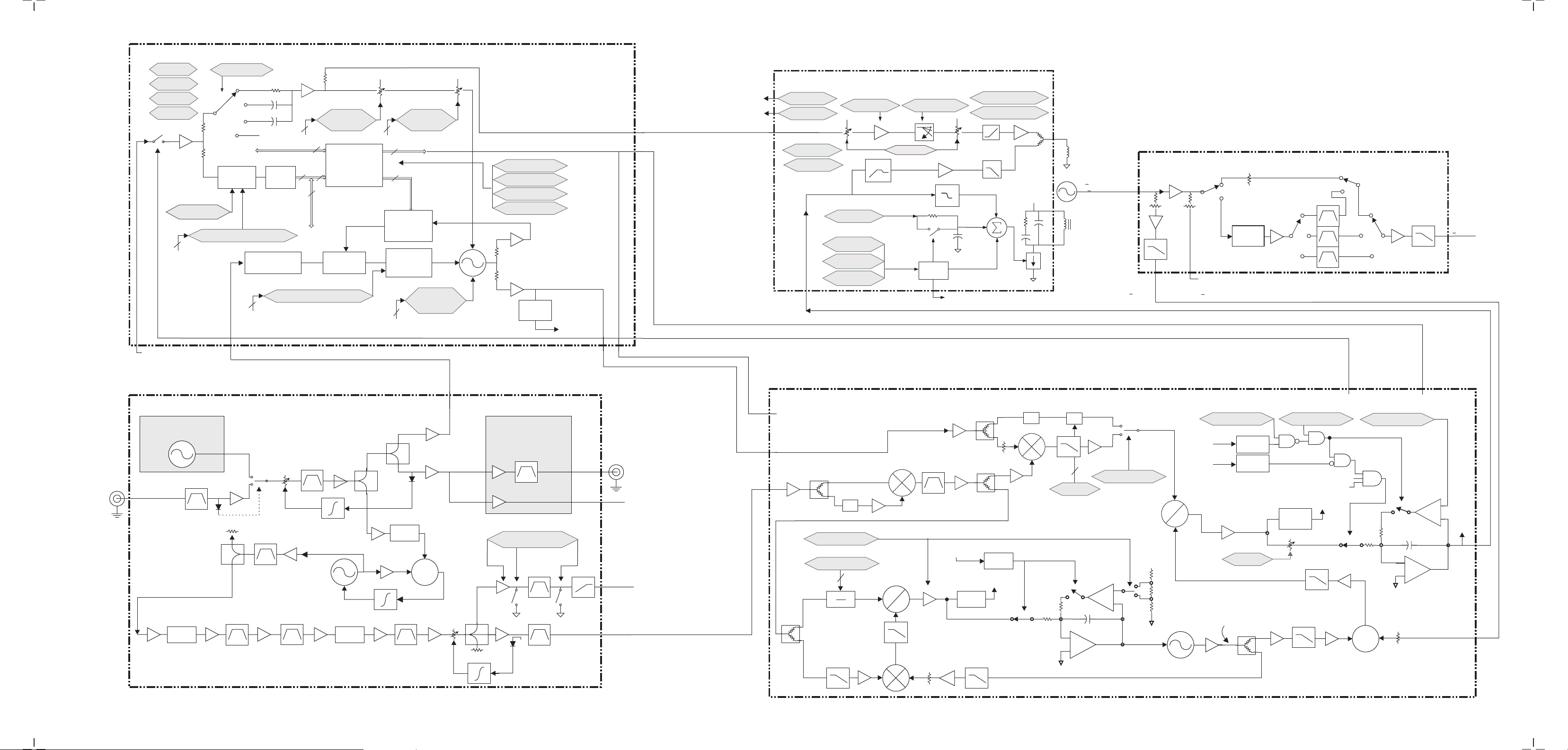
A6 Frac-N (Fine Tune)
H_FM_INV
H_SD_FM
L_SD_OFF
L_FM_OFF
FM_OFF_H
FM_IN_BAND_DAC
7
Reference Input
10 MHz TCXO
MOD_CONTROL
FM
1MHzPM
0.1 MHz PM
Atten &
Offset
FM_IN_BAND_OFFSET_DAC
Reference
Divider /2
7
Control
SD
3
Mod
16
FM
Data I/O
5 MHz
GAIN_CONTROL_DAC
7
5
16
Z
o
FM_OUT_
BAND_
DAC
Frac-N
Prescaler Control
Reclocked
VCO/N
Phase
Detector
9
Source Settled
2
Control
5
Prescaler
Loop Filter &
Lead-Lag
3
ATTEN_
CONTROL
Indicators
EE_POT_
CONTROL
VCO
Tune
VCO
FM
L_RST
L_WIDELBW
L_POS_PHASE_INCR
STRB
10 dB
500-1000 MHz
12 dB
RF
Power
Detector
SOURCE_SETTLED_H
FRACN_SWP_L
ToAnalog Bus
VCO Out
YTO_FM
A9 YIG Driver
V_GHZ_DAC
VSWP_DAC
FM_ATTEN_L
FM_ATTEN_H
PRETUNE_DAC
HOLD_DAC
COMP_DAC
H_SPEEDUP_EN
FM_GAIN_DAC
230: :1k
::
:
:4k
FM_FREQ_COMP
FM_ATTEN
Pretune
Speedup
230
2k
LYO Loop Hold 1
FM_FREQ_COMP_L
FM_FREQ_COMP_H
800k
+32 V
YIG
FM
Coil
Main
Coil
J1
3.2-10 GHz
>
+ 13 dBm
>
A29 20 GHz Doubler
3-10
J4 to A5 Sampler
3.2 - 10 GHz
-7 dBm>
3-10
3-10
5-10
J3 to A6 Frac-N
3.2 - 10 GHz
-7 dBm>
X2
Doubler
10-20
3-10
750 MHz
10-13
16-20
13-16
3-20
Limiter
80 MHz
J2
>3.2 - 20 GHz
14 dBm>
FM Input From
A11 Pulse / Analog
Modulation Generator
A7 Reference (Option UNJ)
A32 10 MHz
Crystal Oscillator
Ext
10 MHz
In
Note: This drawing shows the A7 Reference (Option UNJ).
Both the A7 Reference (Standard) and the A7 Reference (Option UNJ)
have the same input and output signals.
10 MHz
100 MHz
500 MHz
x5
500 MHz
10 MHz
100 MHz
x2
x10
1 GHz
10 MHz to
A6 Frac-N
F
A31 Motherboard
10 MHz
10 MHz Digital Out
1 GHz-OUT_LOWBAND
ON / OFF
1 GHz
1 GHz
50 MHz
Ext
10 MHz
Out
10 MHz
Digital Out to
A11 Pulse / Analog
Modulation Generator
1 GHz
Output to
A8 Output
1 GHz
Output to
A5 Sampler
A5 Sampler / YO Loop (Coarse Tune)
LFNSWP
J6 Frac-N In
500 - 1000 MHz +5dBm
J1 1 GHz In
HIGH_LOW
H_PRESET_EN
750 MHz C
750 MHz
750 MHz B
MULTR
6
M
x ----
256
1 GHz RF
¸4
12 to 155 MHz
250 MHz LO
Mixer IF
LO
F
¦
155 MHz
RF
J1 1 GHz In
750 MHz
MULTR LATCH
+/- 1
STROBE
Unlock
Detector
900 MHz
14 dB
1- Shot
L CRS PLL
UNLK
RF
¸2
LO
L_CRSPLL_Pretune
¸ P
4
FNDIV
_
+
Mode A
Mode B
FM_MODE_A_B
_
+
Vtune
+15V
f
IF
F
YOLGAIN
STROBE
FM MODE
& MULTR
STROBE
¦
Sampler IF
30 to 64 MHz
VCO
H_PRESET_EN
YOLGAIN
f
S
618 to 905 MHz
1 - Shot
0.2 ms
1 - Shot
1.0 ms
FM_OFF_H
L_YOPLL_OPEN
(from YO Driver) LYOSLEW
(from FRAC-N) LFNSWP
L_YOL_UNLK
YO PLL
Unlock
Detector
80 MHz
900 MHz
YO_PREDAC
L_YOPLL_PRESET
L_HOLD
LO
RF
S
f
S
f
YO
SOURCE_SETTLED_H
_
+
_
+
3.2 - 10 GHz From
(A28 YIG Oscillator)
A Bus
YO
Phaselock
se989a
Block Diagram for the Reference / Synthesis Loop
Page 86

Troubleshooting
Reference/Synthesis Loop Block Diagram
1-74
Page 87

Troubleshooting
Reference/Synthesis Loop Block Description
Reference/Synthesis Loop Block Description
The function of the Reference/Synthesis Loop is to establish the frequency characteristics of the signal
generator. These frequency characteristics are the fundamental frequency range, phase noise, and frequency
accuracy. The Reference/Synthesis loop consists of the A7 Reference, A5 Sampler, A6 Frac-N, A9 YIG Driver,
YIG Oscillator (YO), and A29 20 GHz Doubler. The Reference/Synthesis Loop description covers the
generation of 3.2 to 10 GHz signals and the RF Path description covers frequency generation of frequencies
other than 3.2 GHz to 10 GHz.
The basic functions required to generate an accurate frequency are coarse tuning, fine tuning, and output
frequency monitoring or feedback. Coarse tuning is achieved using the Pretune DACs on the A9 YIG Driver.
Fine tuning is achieved using the A5 Sampler and A6 Frac-N. To help explain the operation of the
Reference/Synthesis loop,the following paragraph describeswhat happens when asignal generator is setto a
frequency of 5 GHz.
When theuser enters thefrequency, the A18 CPUsets the A9YIG Driver PretuneDAC to avalue that results
in the YO being coarsely tuned to 5 GHz (within ~ 3 MHz). At thesame time, the CPU sets the Sampler VCO
and theA6 Frac-N VCOto the frequencies necessaryto generate anexact 5 GHz YO output. The output of the
YO is connected to the A29 20 GHz Doubler where a portion of the signal is coupled off and routed to the
A5 Sampler. On the A5 Sampler, the coarsely tuned 5 GHz is converted to an IF frequency and then filtered.
The A6 Frac-N VCO is divided down on the A5 Sampler to approximately the same frequency as the IF from
the coasely tuned YO signal and is used as the reference signal in the phase comparator. The output of the
phase comparator isproportional to the phase (frequency) error between the twosignals. This error voltageis
integrated and summed with the pretune voltage, fine tuning the YO to exactly 5 GHz.
A7 Reference
Essential to frequencyaccuracy and low phasenoise are clean andstable reference signals. Inthis case, there
are two referencesignals required: the 1 GHz signal used by the A5 Samplerand A8 Output, and the 10 MHz
signal used by the A6 Frac-N. The A7 Reference (Standard) uses a 1 GHz STW Oscillator and 10 MHz OCXO.
The low phase noise A7 Reference (Option UNJ) uses a 100 MHz VCXO that is multiplied by 10 to achieve
1 GHz and a high performance 10 MHz OCXO. The A6 Frac-N uses the 10 MHz reference to maintain the
A6 Frac-N's VCO phase coherency.
A5 Sampler
The A5 Sample contains a microwave sampler, used to convert the YO output to lower frequencies for phase
comparison. A portion of the YO's output is coupled to the A5 Sampler to use as the RF input to the sampler.
The VCO on the A5 Sampler is used as the LO input to the sampler. The VCO output is a frequency between
618 to 905 MHz. The LO and RF signals generate an IF signal between 30 and 64 MHz. The IF signal passes
through an 80 MHz low pass filter eliminating all signals above 80 MHz that may pass through the sampler.
The IF signalis an input to a phase comparator. The other phase comparator input is the 10to 80 MHz signal
that is the result of dividing down or mixing the 500 to 1000 MHz signal from the A6 Frac-N VCO. The phase
comparator's output is integrated and the integrated output summed with the pretune voltage on the
A9 YIG Driver to fine tune the YO output to the desired frequency.
In FM OFF mode, the phase noise level is improved on the A5 Sampler by dividing down the A6 Frac-N VCO
signal to get the desired frequency between 10 and 80 MHz. In FM ON mode and rates above 230 Hz, phase
noise performance is not as good as in FM OFF mode because the A6 Frac-N VCO uses a mixer to get the
desired frequency between 10 and 80 MHz. The mixer circuit is needed to allow for higher FM rates.
1-75
Page 88

Troubleshooting
Reference/Synthesis Loop Block Description
A6 Frac-N
One function of the A6 Frac-N is to provide a means to set the YIG Oscillator to any frequency. This is
accomplished on the A6 Frac-N by using a dividing technique that can set the A6 Frac-N VCO signal to any
frequency. The A6 Frac-N VCO output is used as the phase reference for the comparator on the A5 Sampler.
Small changes in the divide number result in small changes in the A6 Frac-N VCO output frequency and
small changes in the YIG Oscillator frequency.
In FM mode, rates 230 Hz and below, FM is accomplished by combining the FM signal and the VCO tune
signal and driving the main coil. For rates above 230 Hz, FM is accomplished using the FM coil circuit on the
A9 YIG Driver and the FM coil in the YIG Oscillator.
A9 YIG Driver
The function of the A9 YIG Driver is to provide the YIG oscillator with the correct power supply and turn
voltages. Coarse tuning s achieved by the A18 CPU setting the pretune DACs to the value needed to tune the
YIG oscillator close to the desired frequency. Correction voltage from the A5 Sampler is summed with the
pretune voltage on the A9 YIG Driver to fine tune the YIG oscillator. For higher rate FM operation, the FM
signal isscaled and the gain calibrated on theA9 YIG Driverbefore being usedto drive the FM coil in theYIG
oscillator.
A28 YIG Oscillator (YO)
The YIG oscillator (YO) output frequency is controlled by the amount of current through the main and FM
coils. The main coil isused for setting CWfrequencies and for FMrates 230 Hzand below. The FMcoil is used
for rates greater than 230 Hz. The YO operates over a frequency range of 3.2 GHz to 10 GHz.
A29 20 GHz Doubler
Internal to the A29 20 GHz Doubler are two couplers used to pick off some of the 3.2 to 10 GHz signal. One
coupled output is routed to the A6 Frac-N and the other coupled output is routed to the A5 Sampler. The
signal to the A5 Sampler provides the feedback needed to generate the fine tune correction voltage used to
control the accuracy of the YIG oscillator frequency.
1-76
Page 89

A9 YIG Driver
V_GHZ_DAC
VSWP_DAC
FM_GAIN_DAC
FM_FREQ_COMP
FM_FREQ_COMP_L
FM_FREQ_COMP_H
A26 Micro Interface Deck
DBL20_AMP_ON_H
DBL20_PATH
6
DBL40_BIAS
2
DBL40_PATH
3
DBL40_LPF
ATT EN
5
DBL40_AMP
FM_ATTEN
FM_ATTEN_L
FM_ATTEN_H
A6 Frac-N
YTO_FM
PRETUNE_DAC
HOLD_DAC
COMP_DAC
H_SPEEDUP_EN
YTO_FM from
A6 Frac-N
230: :1k
A6 Frac-N (Fine Tune)
8.5 GHz
Multi Modulus
Divider
¸
2 / 4 / 8 / 16
6
DIVIDER_CONTROL
A8 Output
Prelevel
Drive
PRE_
LEVEL_
REF_DAC
H_BYPASS
::
:
:4k
230
2k
Pretune
Speedup
LYO Loop Hold 1
LPF_SELECT
Gain
Adj.
GAIN_ADJUST_DAC
OUTPUT_LP_FILTER_SELECT
ALC_MOD_OFFSET_DAC
ALC_MOD_DRIVER_
800k
6
250 MHz
to 4 GHz
BIAS/GAIN_DAC
FM
Coil
YIG
+32 V
Main
Coil
RF
Power
Detector
To
Analog Bus
RF Out
Bypass Mode
Prelevel Detector
ALC
>>3.2 GHz to
10 GHz
+ 13 dBM
J4 to A5 Sampler
To A8 Pre Level Drive
To A 8
MOD_DRIVER_
BIAS/GAIN_DAC
ALC
Mod
OFFSET_DAC
MODLIN_DAC
A29 20 GHz Doubler
3-10
Pulse
3.2 - 10 GHz
MOD_
3-10
-7 dBm>
3-10
J3
3.2 - 10 GHz
-7 dBm>
5-10
1200
MHz
X2
Doubler
850 to
1150
MHz
6dB
10-20
HET_SELECT_L
3dB
1 GHz
Ref
From A7 Reference
400
MHz
3-10
750 MHz
10-13
16-20
13-16
3-20
Limiter
0-3 GHz
0-3.2 GHz
BB_FILTERED
BB_THRU
H_BYPASS
MOD_L_BW
L_RF_OFF_MOD
L_EN_LIN/LOG
L_MODE
L_HOLD_ALC
A30 Modulator Filter
J2
>3.2 - 20 GHz
14 dBm>
ALC
A23 Low Band
Coupler / Detecter
0-2 GHz
MODF_AMP_ON_H
Pulse
MODF_PLS_ENB_L
A10 ALC
Detector
Detector
External
Detector
Hiband
Loband
L ALC Hold
L Pulsed RF Off
AM Input
1
MODF_PATH
10-20
0
2
DETECTOR_SEL
L_Open Loop
L ALC Hold
H_EXP_AM
6
5-8
13-20
8-13
3-5
HIPWRCAL_DAC
LOG_BRKPT_DAC
DET_OFS_DAC
1 kHz
Burst
Comp
_
+
Log
H_LIN_AM
3.2
J3 250 kHz - 3.2 GHz 21 dBm>
Dual Slope Log Amp
H_DET_LPF
L_DETLVLX25
H_DEEP_AM
A27 40 GHz Doubler
J4
10-20 GHz
20 dBm
>
Option 1EA
25 dBm
>
J2 250 kHz - 3.2 GHz 18 dBm
> 3.2 GHz - 20 GHz 18 dBm, Option 1EA 23 dBm
SM Input
I/H
Delay
H_BURST
J1
L_ALC_HOLD_LATCHED
H_SM_MODE
x25
S
S
X2
Doubler
>
>>
H_RF_OFF
+66mV/dB
Det level
Open =
Hold
+
_
Deep
AM
Comp
ALC Ref
Delay
LVL_DAC
-66mV/dBm
A24 Coupler
A25 Detector
2-20 or 2-40 GHz
30 or 40
FM_OFF_H
S
ALC
20-40
GHz
0-20
GHz
J3
ALCMOD_LIN_DAC
ALCMOD_BIAS_DAC
L Unlvl
Interrupt
+
_
_
+
ALCMODGAIN_DAC
H_BELOW_3.2GHZ
-10v
J2
250 kHz - 3.2 GHz 17 dBm
> 3.2 - 20 GHz 15.5 dBm
> 20 GHz 13 dBm
Option 1EA
250 kHz - 3.2 GHz 17 dBm
> 3.2-20 GHz 20.5 dBm
20 GHz 18 dBm
>>
SOURCE_SETTLED_H
Modulation Driver
>
>
>
Exponential
>
>
L_20/
H_40DIG
ADC
MUX
+V
L_20MOD
3.2to20GHz
ALC Mod
Loband ALC Mod
_OFF
ADC
20-26
32-40
26-32
+V
6.8 volts
L_OPENLOOP
Cx1000
Cx100
Cx10
C
_
+
ALC_BW_SEL
1
2
3
all open = 0
Int Out
+10dB/V
FeedFwd
AT1
Attenuator
5/10/40/20/40
Optional
Attenuator
RF
Out
Ext 1,
Front
Panel
Ext 2,
Front
Panel
10 MHz
Digital
FM
A11 Pulse / Analog Modulation Generator
EXT1_50_
OHMS_H
Rin = 600
or 50 ohms
EXT2_50_
OHMS_H
Rin = 600
or 50 ohms
IPGCLK_ON_H
10 MHz
100 MHZ IPG
NSCLK_ON_H
10 MHz
X2
X2
IPGCLK Out
Clock
NSCLK Out
of Lock L
33.554 MHz
NS Clock
EXT1_PEAK_V
of Lock L
NS_CLK
CNTOUT
REF_DAC
EXT1_PEAK_V
REF_DAC
ABUS
IPGCLK
TUNE
ABUS
NSCLK
TUNE
NS_Reset
NS_Address
NS_Data
-10Vref
-10Vref
IPG_CLK
"Elsie" NS
OCA
ODBUS
OCC
FM2_SCALE_DAC
Peak
Detect
Peak
Detect
12
12
A Bus
Abus
Ext1_High_H
Ext1_low_H
Abus
Ext2_High_H
Ext2_low_H
Latch
Data
Clock
Clock
Data
Latch
Gate / Pulse /
Trigger Input,
Front Panel
EXT1_AC_H
EXT2_AC_H
DAC
12
Data
Clock
Clock
12
Data
DAC
FM_OFFSET1
+
S
+
-
_DAC
FM_OFFSET2
_DAC
-
FGEN1_OFFSET_
DAC
FGEN2_OFFSET_
DAC
-
FM1_MUX
FM2_MUX
MOD_MUX
A Bus
S
-
-
S
FM
A Bus
F_Gen 2
External 1
External 2
External 2
F_Gen 1
External 1
Audio 1
Audio 2
F_GEN1
F_GEN2
AM
Vref
+
_
PULSE IN SEL
PG_MODE
PG_TRIGGER_INVERT
PG_PULSE_REP_INTERVAL
PG_PULSE_REP_INTERVAL
PG_VIDEO_BEGIN
PG_VIDEO_END
PG_SYNC_BEGIN
PG_SYNC_END
AM1_MUX
AM2_MUX
LF_OUT_DAC
A Bus
Internal Pulse Generator
PULSE_OUT_SEL
FED_VREF_DAC
FED_PULSE_SEL
RED_PULSE_SEL
RED_VREF_DAC
PULSE_ED_SEL
VIDEO_OUT_EN_L
SYNC_OUT_EN_L
AM1_DAC
AM_OFFSET
_DAC
AM2_DAC
50 ohm
L Pulsed
RF Off
A Bus
A Bus
ABus
50 ohm
50 ohm
ABus
+
-
S
+
A Bus
Video Ou t
A Bus
Sync Out
AM
LFO
Front Panel
se990a
Block Diagram for the RF Path
Page 90

Troubleshooting
RF Path Block Diagram
1-78
Page 91

Troubleshooting
RF Path Block Description (Frequency Generation, Level Control, and Modulation)
RF Path Block Description
(Frequency Generation, Level Control, and Modulation)
Frequency Generation
The RF is used to generate, modulate and control the level of the output frequencies. The Synthesis Loop
Block Description describes how the fundamental frequencies of 3.2 GHz to 10 GHz are generated using the
YO, Sampler, and Frac-N. Frequencies below 3.2 GHz are generated by dividing down the fundamental
frequency. Output frequencies between3.2 and 10 GHz are the RF fundamental frequencies generated by the
YIG Oscillator. Output frequencies of 10 and 20 GHz are generated by doubling the 5to 10 GHz fundamental
frequency. Output frequencies above20 GHz are generated by doubling the 10 to 20 GHz frequencies. The RF
Path consists of the A29 20 GHz Doubler, A6 Frac-N, A8 Output, A30 Modulation Filter, and A27 40 GHz
Doubler.
A29 20 GHz Doubler
Besides providing signal to the A5 Sampleras discussed in SynthesisLoop overview, the A29 20GHz Doubler
is a key par of theRF path. For output frequencies below3.2 GHz, the A2920 GHz Doubler providesRF input
to the A6 Frac-N For output frequencies 3.2 to 10 GHz, the A29 20 GHz Doubler passes through the YIG
Oscillator frequencies. For output frequencies of 10 to 20 GHz, the A29 20 GHz Doubler doubles the 5 to
10 GHz fundamental. For frequencies 3.2 GHz and above, the A29 20 GHz Doubler output is routed to the
A30 Modulation Filter.
A6 Frac-N
The A6 Frac-N is part of the Synthesis Loop and the RF path. Frequencies below 3.2 GHz are generated on
the A6Frac-N by dividing down the fundamental frequency. Frequencies above 3.2 GHz do notgo through the
A6 Frac-N. On the A6 Frac-N, the RF signal from the A29 20 GHz Doubler is amplified, filtered, divided, and
then amplified again before being routed to the A8 Output.
A pre-level bias voltage from the A8 Output is fed back to the A6 Frac-N to maintain the desired RF output
level from the A6 Frac-N to the A8 Output. If the A8 Output is removed from the signal generator while the
signal generator is powered on, thecorrect bias is maintainedand the RF powerlevel to the A8Output can be
checked.
A8 Output
The A8Output provides pre-level biasvoltage to the A6 Frac-N,RF output leveling control,pulse modulation,
and amplitude modulation, and frequency under range circuitry. The ALC diode is used to control the RF
output power for frequencies up to 3.2 GHz. With no bias applied to the ALC diode output power goes to the
minimum levelthe circuit can provide. In closed loopoperation, the A10ALC uses a negativevoltage from the
detectors to maintain the bias on the ALC diode. Pulse modulation (RF pulsed on) is achieved by applying a
+5 Vdc tothe pulse circuitry on the A8 Output. Under rangefrequencies below 250 MHz aregenerated on the
A8 Output by mixing the RF signal with a 1 GHz signal from the A7 Reference. The A8 Output signals pass
through the A23 Low Band Coupler/Detector before going to the A30 Modulation Filter.
1-79
Page 92

Troubleshooting
RF Path Block Description (Frequency Generation, Level Control, and Modulation)
A30 Modulation Filter
The A30 Modulation Filter’s frequency output is from 100 kHz to 20 GHz. Frequencies below 3.2 GHz are
switched through the A30 Modulation Filter and are not filtered or modulated in the assembly. The A30
Modulation Filter provides level control, pulse modulation, amplitude modulation, and filtering for
frequencies 3.2 GHz and above. The ALC diode is used to maintain level control. With not bias applied to the
ALC diode, output goes to the maximum power level the circuit can produce. In pulse operation, the pulse
diode is biased on for an RF signal topass through. If an A11 Pulse/AnalogModulation Generator is installed
and a bias is not applied to the pulse diode, no RF signal will pass through. Since the same A30 Modulation
Filter is used in all models, if an A11 Pulse/Analog Modulation Generator is not installed, circuitry on the
A30 Modulation Filter biases the pulse diode on.
In a 20 GHz signal generator the A30 Modulation Filter output is routed to the A24 High Band Coupler and
A25 High Band Detector. If a 40 GHz Doubler is installed, two A30 Modulation Filter outputs are routed to
the A27 40 GHz Doubler.
A27 40 GHz Doubler
The 40 GHz Doubler is used to produce frequencies between 20 and 40 GHz. The 40 GHz Doubler has two
inputs from the A30 Modulation Filter. One input is used for frequencies below 20 GHz and one for
frequencies above 20 GHz. Frequencies below 20 GHz pass through the A27 40 GHz Doubler. Frequencies
20 GHz and above are generated by doubling the A30 Modulation Filter’s 10 to 20 GHz input. After being
doubled, band pass filters are used toeliminate unwanted harmonics.The 40 GHz outputis routed to theA24
High Band Coupler and A25 Detector.
A23 Low Band Coupler/Detector, A24 High Band Coupler, and A25 High Band Detector
The function of the coupler is to couple off a portion of the RF signal. The detector is used to convert the RF
signal to a dc voltage. The dc voltage is then routed to the A10 ALC. The RF signal out of the A23 Low Band
Coupler/Detector isrouted to the A30Modulation Filter. The RFsignal out ofthe A24 High Band Coupler and
A25 High Band Detector is routed to either the optional attenuator or the RF output connector. The A23 Low
Band Coupler/Detector is s single unit and the coupler and detector must be changed together. The A24 High
Band Coupler and A25 High Band Detector are two separate units and can be changed independently. The
A23 Low Band Coupler/Detector is used for frequencies 2 GHz and below. The A24 High Band Coupler and
A25 High Band Detector are used for frequencies above 2 GHz.
ALC Loop
The function of the ALC loop is to maintain power level accuracy by measuring the output power and
compensating for deviations from the set power level. The A23 Low BandCoupler/Detector and the A24 High
Band Coupler and A25 High Band Detector detect the output power level, compare the detected voltage to a
reference, and adjust the modulator diodes (located on the A8 Output and A30 Modulation Filter) to achieve
the desired power level.
A10 ALC
In ALC ON operation, the A10 ALC integrates the detected and reference voltages and adjusts the drive to
the modulator diodes until both the reference and detected voltages agree. The low and high band detectors
provide the detected voltage to the A10 ALC. The reference voltage is determined by the A18 CPU setting
DACs on theA10 ALC. Thedetected and reference voltagesare the input to an integrator.When the inputs to
the integrator are equal the output ramps in either direction changing the modulator diode drive level. Once
the detected voltage equals the reference voltage the output of the integrator remains at a constant level.
1-80
Page 93

Troubleshooting
RF Path Block Description (Frequency Generation, Level Control, and Modulation)
ALC ON operation is referred to as a closed loop operation because the output signal level is continually
monitored and used to adjust the modulator drive resulting unleveled output power.
In ALC OFF mode, the feedback path, the detected voltage path is opened and only the reference voltage is
used to set the output power level. Because the feedback path is open, ALC OFF mode is referred to as open
loop operation. With the modulator level is set to a fixed drive level and without the output level being
monitored, the RF output level will vary.
In external leveling operation, internal detector voltages are replaced withan external detector voltages. The
external detector must be a negative detector to provide the correct signal to the A10 ALC. Leveling accuracy
is a function of the detector and instrument calibration. Since the instrument is calibrated with internal
detectors, leveling accuracy in external mode is dependent on the detector being used.
The ALC circuit is temperature compensated to provide leveled performance over a specified temperature
range, The high band diode temperature sensing circuit is located on the RF deck on the A24 High Band
Coupler and A25High Band Detector. A resistor pack isused to calibrate the highband detector performance
over temperature. If the A25 Detector is replaced, the resistor pack provided with the detector must also be
installed to maintain maximum performance. The low band detector can not be replace independently of the
coupler, so temperature compensation is contained within the assembly. Although rare, unstable level
performance can be the result of problems with poorly soldered resistors on the resistor pack or with other
components in the temperature compensation circuit.
Modulation (AM, FM, PM, and Pulse)
Modulation features apply only to analog versions of signal generators. The A11 Pulse/Analog Modulation
Generator provides modulation signals for AM, FM, pulse, and phase. A dual function generator is built onto
the A11 Pulse/Analog Modulation Generator and tied to the 10 MHz reference from A7 Reference for phase
synchronization. Pulse Input, EXT1, and EXT2 provide external modulation input connections. A low
frequency output (LF Output) connector located on the front panel can be selected to output the signal
generated by the A11 Pulse/Analog Modulation Generator to drive other instruments. SYNC OUT and
VIDEO OUT signals are also generated on the A11 Pulse/Analog Modulation Generator.
EXT 1 and EXT 2 inputs have modulation drive level detection circuits and generate error messages if too
small or too large of a signal is applied to the input. EXT 1 and EXT 2 can be set for 50 or 600 ohms input
impedance and can be configured for dc or ac coupling. The FM/PM modulation signal is routed to the
A6 Frac-N. FM rated of less than 4 kHz are applied to both prescale circuit for the A6 Frac-N VCO and to the
A6 Frac-N VAC’s tune voltage to achieve FM. The prescale circuit modifies the VCO feedback signal to the
VCO phase detector causing a change in the VCO frequency. FM rates of 4 kHz to 100 kHz are applied to the
A6 Frac-N VCO.FM rates above 100 kHz are routed from the A6 Frac-N to the A9 YIG Driver and applied to
the FM coil in the YIG Oscillator. Phase modulation is achieved by applying the same signal used for FM to
the A6 Frac-N, where the signal goes through an added LCR circuit for PM. The modulation signal is then
routed in the same manner as when FM is used.
The AM signal is routed to the ALC where it is summed with the ALC reference voltage and applied to the
Modulation Filterand Output ALC diodes. Pulsemodulation signals arerouted directly tothe Output andthe
Modulation Filter pulse diodes. Pulse diodes must be biased on for RF to pass through. Because the ALC
bandwidth is limited, the ALC cannot properly level the RF output with pulse widths of <1 microsecond. To
compensate for leveling limitations at faster pulse rates, Search Mode operation has been added. In Search
Mode, the signal generator turns off all modulation, levels the power using closed loop operation (feedback),
then opens the loop and levels usingthe leveling voltage determinedduring closed loop operation.Changes in
power level,frequency, or pulsesettings will causethe signal generatorto turn modulationoff, levelthe power
with thenew settings, then open the loopand turn modulationback on. Becausedrift in levelcircuits with out
feedback control can occur over time, it is not recommended to leave Search node on for extended periods
without closing the loop and resetting the leveling voltage.
1-81
Page 94

Troubleshooting
Self-Test Overview
Self-Test Overview
Philosophy
The philosophy of self-test is, “It is better to pass a defective signal generator than to fail a good signal
generator. Self-tests are designed as a diagnostic tool used to check signal generator hardware. Self-tests do
not require the signalgenerator to be calibrated before self-tests will pass. This philosophy implies that some
failures will not be detected and reported as bad, but will pass. If the signal generator powers on and
self-tests can be run, troubleshooting should always start by running self-tests and resolving reported
problems first.
Overview
Embedded in the signal generator’s firmware is a group of tests (self-tests) that can be used to evaluate the
condition of the circuitry on many of the assemblies. Self-tests check hardware performance under controlled
conditions and compare test results to predetermine limits. If the results fall within the limits the signal
generator passes. If one or more test results fall outside the limits,the self-test routine evaluates the failures
and reports the most independent failure.
How self-test works:
1. When the signal generator is tested at the factory, self-test limits are loaded into the A18 CPU memory
from devices on each assembly or from fixed files. Most assemblies contain limit information while
microcircuit limits must be loaded.
2. When the program runs, latches and DACs are set to a known state.
3. An analog mux routes the detected dc signal from the selected rest node to the A18 CPU.
4. The A18 CPU compares the detected dc level to the test limit. If thedetected value is withinthe limits, the
A18 CPU reports a pass.
5. If one or more detected values fall outside the limits, the most independent failure is determined and
reported.
Independent failures
Independent failures can best be understood by using an example. There are three assemblies in a series. A1
is the firstassembly, A2 the second assembly,and A3 the thirdassembly. A1 output is theinput for A2 andA2
output is the input for A3. If A1 output is bad, A2and A3 pouts are also bad. If A2 output is bad, A3 output is
bad. A file in the signal generator contains this dependency knowledge for the signal generator to use to
identify the most independent failure. If A1, A2, and A3 self-tests all fail, the signal generator reports A1 as
the most independent failure. If A1 passes but A2 and A3 fail, self-test reports A2 as the most independent
failure. If A2 passes and A3 fails, self-test reports A3 as the most independent failure. If two independent
failures occur, self-test reportsonly one failure ata time and reports the second failure after thefirst reported
failure is repaired.
The troubleshooting procedure is based on the most independent failure and no lower level information is
needed. Although not needed for troubleshooting the signal generator, the self-test overhead provides
features to view lower level detailed information about the subroutines and select specific routines to run.
These features include:
• Select/Deselect Test
• Select/Deselect All
• View Details
• Run Highlighted Tests
1-82
Page 95

Troubleshooting
Self-Test Overview
• Run Selected Tests
• When View Details is selected, the measured value, lower, and upper limits are displayed or the
highlighted test.
1-83
Page 96

Troubleshooting
Contacting Agilent Technologies
Contacting Agilent Technologies
If you shouldhave a problem with your signal generator, contact your nearest salesand service offices. Before
calling, please be prepared to provide the following information:
• a complete description of the failure
• is there a reported failure (Y or N) and what is the failure being reported
• was the failure dead on arrival (DOA) or did the instrument work before use
• the model number, all options, and serial number of the instrument
• the firmware revision date
• has self-test been run (Y or N)
Review the Warranty
If there is still a problem, read the warranty printed in Chapter 5. If your signal generator is covered by a
separate maintenace agreement, be familiar with its terms.
Agilent Technologies offers several maintenance plans to service your signal generator after warranty
expiration. Call your Agilent Technologies sales and service office for full details.
1-84
Page 97

Troubleshooting
Contacting Agilent Technologies
Contacting Agilent Sales and Service Offices
Before contacting Agilent, read the warrantyprinted in Chapter 5.If your signal generator is covered under a
main ten ace agreement, be familiar with its terms.
Sales and service offices are located around the world to provide complete support for your signal generator.
To obtain servicing information, contact the nearest Agilent Sales and Service office listed in Table1-44. For
information on ordering parts refer to Chapter 3.
By internet, phone, or fax, get assistance with all your test and measurement needs.
Table 1-44 Contacting Agilent
Online assistance: www.agilent.com/find/assist
United States
(tel) 1 800 452 4844
New Zealand
(tel) 0 800 738 378
(fax) (+64) 4 495 8950
Latin America
(tel) (305) 269 7500
(fax) (305) 269 7599
Japan
(tel) (+81) 426 56 7832
(fax) (+81) 426 56 7840
Canada
(tel) 1 877 894 4414
(fax) (905) 282-6495
Australia
(tel) 1 800 629 485
(fax) (+61) 3 9210 5947
Asia Call Center Numbers
Country Phone Number Fax Number
Singapore 1-800-375-8100 (65) 836-0252
Malaysia 1-800-828-848 1-800-801664
Philippines (632) 8426802
Thailand (088) 226-008 (outside Bangkok)
Hong Kong 800-930-871 (852) 2506 9233
Taiwan 0800-047-866 (886) 2 25456723
People’s Republic of
China
India 1-600-11-2929 000-800-650-1101
1-800-16510170 (PLDT Subscriber Only)
(662) 661-3999 (within Bangkok)
800-810-0189 (preferred)
10800-650-0021
(632) 8426809
1-800-16510288 (PLDT
Subscriber Only)
(66) 1-661-3714
10800-650-0121
Europe
(tel) (+31) 20 547 2323
(fax) (+31) 20 547 2390
In any correspondence or telephone conversation, refer to the signal generator by its model number and full
serial number. With this information, the Agilent representative can determine whether your unit is still
within its warranty period.
Important Information Needed by an Agilent Service Representative
Be as specific as possible about the nature of the problem and include information such as:
• any error messages that appeared on the signal generator
• a complete performance test record from the calibration guide for your signal generator
• any other specific data on the performance of the signal generator
1-85
Page 98

Troubleshooting
Contacting Agilent Technologies
Returning Your Signal Generator for Service
Use the information in this section if you need to return the signal generator to Agilent Technologies.
Packaging the Signal Generator
1. Use the original packaging materials or a strong shipping container that is made of double-walled,
corrugated cardboard with 159 kg (350 lb.) bursting strength. The carton must be both large enough and
strong enough to accommodate the signal generator and allow at least 3 to 4 inches on all sides of the
signal generator for packing material.
CAUTION Signal generator damage can result from usingpackaging materials other thanthose specified.
Never use styrene pellets, in any shape, as packaging materials. They do not adequately
cushion the instrument or prevent it from shifting in the carton. Styrene pellets cause
equipment damage by generating static electricity and by lodging in the signal generator
fan.
2. Surround the instrument with at least 3 to 4 inches of packing material, or enough to prevent the
instrument from moving in the carton. If packing foam is not available, the best alternative is SD-240 Air
Cap
™ from Sealed Air Corporation (Hayward, CA 94545). Air Cap looks like a pink plastic sheet covered
with 1-1/4 inchair-filled bubbles. Usethe Air Cap to reduce staticelectricity. Wrap the instrument several
times in the material to both protect the instrument and prevent it from moving in the carton.
3. Seal the shipping container securely with strong, nylon adhesive tape.
4. Mark the shipping container “FRAGILE, HANDLE WITH CARE” to ensure careful handling.
5. Retain copies of all shipping papers.
1-86
Page 99

2 Assembly Replacement
2-1
Page 100

Assembly Replacement
Before You Replace an Assembly
Before You Replace an Assembly
CAUTION Many of the assemblies in this instrument are very susceptible to damage from electrostatic discharge (ESD).
Perform service procedures only at a static-safe workstation and wear a grounding strap.
Be sure to review the warning and caution statements described in Chapter 55, "Safety and Regulatory," on page 5-1, prior to
replacing an assembly in your signal generator.
After Replacing or Repairing an Assembly
After you have replaced or repaired an assembly, certain performance tests and adjustments may have to be performed. Please
refer to Chapter 54, "Post-Repair Procedures," on page 5-1, for the list of performance tests and adjustments required for each
assembly.
2-2
 Loading...