


General Purpose, Low Noise
NPN Silicon Bipolar Transistor
Technical Data
AT-41511
AT-41533
Features
• General Purpose NPN
Bipolar Transistor
• 900 MHz Performance:
AT-41511: 1 dB NF, 15.5 dB G
AT-41533: 1 dB NF, 14.5 dB G
• Characterized for 3, 5, and
8 Volt Use
• SOT-23 and SOT-143 SMT
Plastic Packages
• Tape-and-Reel Packaging
Option Available
[1]
Outline Drawing
EMITTER COLLECTOR
415
BASE EMITTER
SOT 143 (AT-41511)
COLLECTOR
415
Description
Agilent’s AT-41511 and AT-41533
are general purpose NPN bipolar
transistors that offer excellent
high frequency performance at an
A
economical price. The AT-41533
A
uses the 3 lead SOT-23, while the
AT-41511 places the same die in
the lower parasitic 4 lead SOT-
143. Both packages are industry
standard, and compatible with
high volume surface mount
assembly techniques.
The 4 micron emitter-to-emitter
pitch of these transistors yields
high performance products that
can perform a multiplicity of
tasks. The 14 emitter finger
interdigitated geometry yields an
intermediate-sized transistor with
easy to match to impedances, low
noise figure, and moderate
power.
Optimized for best performace
from a 5 to 8 volt bias supply,
these transistors are also good
performers at 2.7 V. Applications
include use in wireless systems as
an LNA, gain stage, buffer,
oscillator, or active mixer.
An optimum noise match near
50 ohms at 900 MHz makes these
devices particularly easy to use as
LNAs. Typical amplifier designs
at 900 MHz yield 1 dB noise
figures with 15 dB or more
associated gain at a 5 V, 5 mA
bias, with good gain and noise
figure obtainable at biases as low
as 2 mA.
The AT-415 series bipolar
transistors are fabricated using
Agilent’s 10 GHz fT Self-AlignedTransistor (SAT) process. The die
are nitride passivated for surface
protection. Excellent device
uniformity, performance and
reliability are produced by the
use of ion-implantation, selfalignment techniques, and gold
metalization in the fabrication of
these devices.
BASE EMITTER
SOT 23 (AT-41533)
1. Refer to “Tape-and-Reel Packaging for
Semiconductor Devices.”
2
AT-41511, AT-41533 Absolute Maximum Ratings
Absolute
Symbol Parameter Units Maximum
V
V
V
T
EBO
CBO
CEO
I
C
P
T
T
STG
j
Emitter-Base Voltage V 1.5
Collector-Base Voltage V 20
Collector-Emitter Voltage V 12
Collector Current mA 50
Power Dissipation
[2,3]
mW 225
Junction Temperature °C 150
Storage Temperature °C -65 to 150
[1]
Thermal Resistance:
θ
=550°C/W
jc
Notes:
1. Operation of this device above any one
of these parameters may cause
permanent damage.
2. T
Mounting Surface
3. Derate at 1.82 mW/°C for TC > 26°C.
= 25°C.
[2]
Electrical Specifications, TA = 25°C
AT-41511 AT-41533
Symbol Parameters and Test Conditions Units Min Typ Max Min Typ Max
h
I
CBO
I
EBO
FE
Forward Current Transfer Ratio VCE = 5 V - 30 150 270 30 150 270
IC = 5 mA
Collector Cutoff Current VCB = 3 V µA 0.2 0.2
Emitter Cutoff Current VEB = 1 V µA 1.0 1.0
Characterization Information, TA = 25°C
AT-41511 AT-41533
Symbol Parameters and Test Conditions Units Min Typ Min Typ
NF Noise Figure f = 0.9 GHz dB 1.0 1.0
VCE = 5 V, IC = 5 mA f = 2.4 GHz 1.7 1.6
G
Associated Gain f = 0.9 GHz dB 15.5 14.5
A
VCE = 5 V, IC = 5 mA f = 2.4 GHz 11 9
P
1dB
Power at 1 dB Gain Compression (opt tuning) f = 0.9 GHz dBm 14.5 14.5
VCE = 5 V, IC = 25 mA
G
1dB
Gain at 1 dB Gain Compression (opt tuning) f = 0.9 GHz dB 17.5 14.5
VCE = 5 V, IC = 25 mA
IP
Output Third Order Intercept Point, f = 0.9 GHz dBm 25 25
3
VCE = 5 V, IC =25 mA (opt tuning)
2
|S
|
21E
Gain in 50 Ω system; VCE = 5 V, IC = 5 mA f = 0.9 GHz dB 13.5 15.5 10.8 12.8
f = 2.4 GHz 7.9 5.2
Ordering Information
Part Number Increment Comments
AT-41511-BLK 100 Bulk
AT-41511-TR1 3000 7" Reel
AT-41533-BLK 100 Bulk
AT-41533-TR1 3000 7" Reel
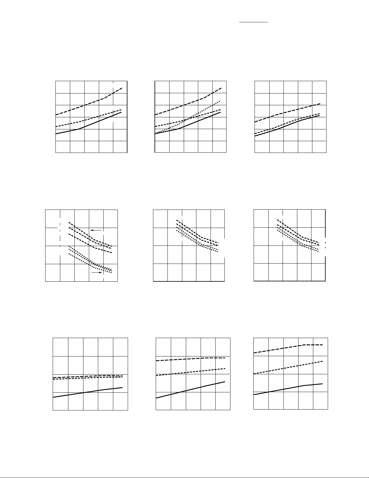
AT-41511, AT-41533 Typical Performance
3
3.0
2.5
2.0
1.5
1.0
NOISE FIGURE (dB)
0.5
0
0.1
1.1
0.6 2.1 2.6
FREQUENCY (GHz)
1.6
Figure 1. AT-41511 and AT-41533
Minimum Noise Figure vs. Frequency
and Current at VCE = 2.7 V.
20
10, 25 mA
5
5 mA
2 mA
10, 25 mA
5 mA
2 mA
PKG 11
15
10
PKG 11 (dB)
a
G
25 mA
10 mA
2, 5 mA
25
20
15
10
3.0
2.5
2.0
1.5
1.0
NOISE FIGURE (dB)
0.5
0
0.1
1.1
0.6 2.1 2.6
FREQUENCY (GHz)
1.6
Figure 2. AT-41511 and AT-41533
Minimum Noise Figure vs. Frequency
and Current at VCE = 5 V.
20
PKG 11
15
PKG 33
10
(dB)
a
G
PKG 33 (dB)
a
G
5
25 mA
2 mA
10 mA
5 mA
10, 25 mA
5 mA
10, 25 mA
5 mA
3.0
2.5
2.0
1.5
1.0
NOISE FIGURE (dB)
0.5
0
0.1
0.6 2.1 2.6
FREQUENCY (GHz)
1.1
1.6
25 mA
10 mA
5 mA
Figure 3. AT-41511 and AT-41533
Minimum Noise Figure vs. Frequency
and Current at VCE = 8 V.
20
PKG 11
15
(dB)
a
G
PKG 33
10
5
10, 25 mA
5 mA
10, 25 mA
5 mA
0
0.1
0.6 2.1 2.6
FREQUENCY (GHz)
PKG 33
1.61.1
Figure 4. AT-41511 and AT-41533
Associated Gain vs. Frequency and
Current at VCE = 2.7 V.
20
15
10
(dBm)
1 dB
P
5
0
0.1
1.1
0.6 2.1 2.6
FREQUENCY (GHz)
1.6
25 mA
10 mA
5 mA
Figure 7. AT-41511 and AT-41533
P
vs. Frequency and Bias at
1dB
VCE= 2.7 V, with Optimal Tuning.
5
0
0.6 2.1 2.6
0.1
1.1
FREQUENCY (GHz)
1.6
Figure 5. AT-41511 and AT-41533
Associated Gain vs. Frequency and
Current at VCE = 5 V.
20
15
10
(dBm)
1 dB
P
5
0
0.1
1.1
0.6 2.1 2.6
FREQUENCY (GHz)
1.6
25 mA
10 mA
5 mA
Figure 8. AT-41511 and AT-41533
P
vs. Frequency and Bias at
1dB
VCE= 5 V, with Optimal Tuning.
0
0.1
0.6 2.1 2.6
FREQUENCY (GHz)
1.1
1.6
Figure 6. AT-41511 and AT-41533
Associated Gain vs. Frequency and
Current at VCE = 8 V.
20
25 mA
15
10 mA
10
(dBm)
1 dB
P
5
0
0.1
0.6 2.1 2.6
FREQUENCY (GHz)
1.1
1.6
Figure 9. AT-41511 and AT-41533
P
vs. Frequency and Bias at
1dB
VCE= 8 V, with Optimal Tuning.
5 mA

4
GAIN (dB)
0
30
0
FREQUENCY (GHz)
145
25
15
5
3
20
10
2
MSG
MAG
MSG
S21
GAIN (dB)
0
30
0
FREQUENCY (GHz)
145
25
15
5
3
20
10
2
MSG
MAG
MSG
S21
AT-41511 Typical Scattering Parameters, Common Emitter, Zo = 50 Ω, VCE = 2.7 V, IC = 5 mA
Freq. S
11
GHz Mag Ang dB Mag Ang dB Mag Ang Mag Ang
0.1 0.84 -27 23.44 14.854 161 -34.89 0.018 76 0.95 -11
0.5 0.59 -102 19.01 8.924 115 -24.88 0.057 48 0.65 -34
0.9 0.49 -141 15.09 5.684 93 -22.97 0.071 43 0.51 -39
1.0 0.48 -149 14.30 5.189 89 -22.73 0.073 43 0.49 -39
1.5 0.46 -176 11.15 3.61 72 -21.21 0.087 44 0.44 -43
1.8 0.46 170 9.69 3.051 64 -20.26 0.097 45 0.43 -45
2.0 0.46 162 8.86 2.774 59 -19.74 0.103 45 0.42 -47
2.4 0.47 148 7.37 2.337 50 -18.64 0.117 46 0.42 -51
3.0 0.5 130 5.58 1.901 36 -17.14 0.139 45 0.41 -59
4.0 0.56 106 3.25 1.454 17 -14.89 0.18 42 0.4 -73
5.0 0.61 87 1.36 1.17 0 -12.96 0.225 37 0.4 -91
S
21
S
12
S
22
AT-41511 Typical Noise Parameters,
Common Emitter, Z
Freq F
= 50 Ω, V
o
min
GHz dB Mag Ang -
0.1 0.8 0.45 6 0.25
0.9 1.0 0.39 63 0.19
1.8 1.4 0.32 137 0.12
2.4 1.7 0.40 177 0.09
= 2.7 V, I
CE
Γ
opt
= 5 mA
C
R
n
AT-41533 Typical Scattering Parameters, Common Emitter, Zo = 50 Ω, VCE = 2.7 V, IC = 5 mA
Freq. S
GHz Mag Ang dB Mag Ang dB Mag Ang Mag Ang
0.1 0.78 -30 23.43 14.834 155 -33.98 0.020 75 0.94 -12
0.5 0.35 -99 16.91 7.004 103 -24.58 0.059 60 0.62 -28
0.9 0.23 -144 12.50 4.219 84 -21.21 0.087 62 0.55 -30
1.0 0.21 -154 11.65 3.826 80 -20.54 0.094 63 0.54 -31
1.5 0.20 162 8.50 2.661 64 -17.46 0.134 64 0.52 -36
1.8 0.22 144 7.09 2.261 56 -15.97 0.159 63 0.51 -40
2.0 0.23 134 6.30 2.065 51 -15.09 0.176 63 0.51 -42
2.4 0.26 118 4.97 1.773 42 -13.39 0.214 61 0.50 -48
3.0 0.30 101 3.45 1.488 30 -11.21 0.275 56 0.48 -58
4.0 0.37 80 1.66 1.211 13 -8.20 0.389 46 0.45 -80
5.0 0.44 62 0.35 1.041 -1 -5.90 0.507 33 0.42 -104
11
AT-41533 Typical Noise Parameters,
Common Emitter, Z
Freq F
GHz dB Mag Ang -
0.1 0.7 0.45 8 0.20
0.9 1.0 0.25 94 0.13
1.8 1.4 0.38 -159 0.08
2.4 1.6 0.54 -122 0.16
o
= 50 Ω, V
min
= 2.7 V, I
CE
Γ
opt
S
21
= 5 mA
C
Figure 10. AT-41511 Gains vs.
Frequency at VCE = 2.7 V, IC = 5 mA.
S
12
R
n
Figure 11. AT-41533 Gains vs.
Frequency at VCE = 2.7 V, IC = 5 mA.
S
22

5
GAIN (dB)
0
30
0
FREQUENCY (GHz)
145
25
15
5
3
20
10
2
MSG
MAG
MSG
S21
AT-41511 Typical Scattering Parameters, Common Emitter, Zo = 50 Ω, VCE = 2.7 V , IC = 25 mA
Freq. S
11
S
21
S
12
S
22
GHz Mag Ang dB Mag Ang dB Mag Ang Mag Ang
0.1 0.49 -91 29.26 29.048 136 -37.72 0.013 62 0.73 -22
0.5 0.53 -168 18.55 8.459 92 -30.46 0.030 61 0.45 -23
0.9 0.53 172 13.62 4.798 79 -26.56 0.047 66 0.42 -26
1.0 0.53 169 12.73 4.330 76 -25.68 0.052 67 0.42 -27
1.5 0.54 153 9.34 2.932 63 -22.50 0.075 67 0.42 -34
1.8 0.55 145 7.86 2.473 57 -21.01 0.089 66 0.42 -38
2.0 0.56 140 6.97 2.232 52 -20.09 0.099 66 0.42 -41
2.4 0.57 129 5.47 1.877 44 -18.49 0.119 64 0.42 -48
3.0 0.60 116 3.67 1.525 32 -16.54 0.149 59 0.41 -58
4.0 0.64 95 1.30 1.162 14 -13.98 0.200 51 0.40 -75
5.0 0.67 79 -0.58 0.935 -1 -11.90 0.254 43 0.39 -96
AT-41511 Typical Noise Parameters,
Common Emitter, Z
Freq F
= 50 Ω, V
o
min
GHz dB Mag Ang -
0.1 1.6 0.13 18 0.16
0.9 1.9 0.24 -162 0.13
1.8 2.3 0.40 -137 0.23
2.4 2.7 0.50 -122 0.35
= 2.7 V, I
CE
Γ
opt
= 25 mA
C
R
n
AT-41533 Typical Scattering Parameters, Common Emitter, Z
Freq. S
GHz Mag Ang dB Mag Ang dB Mag Ang Mag Ang
0.1 0.34 -75 29.37 29.404 127 -37.08 0.014 72 0.71 -21
0.5 0.19 -168 17.63 7.614 88 -25.68 0.052 76 0.47 -20
0.9 0.20 161 12.73 4.329 74 -20.82 0.091 74 0.46 -24
1.0 0.20 154 11.84 3.909 71 -19.91 0.101 74 0.45 -26
1.5 0.24 132 8.56 2.679 59 -16.42 0.151 70 0.45 -33
1.8 0.25 121 7.12 2.271 52 -14.85 0.181 67 0.44 -38
2.0 0.27 115 6.32 2.071 47 -13.94 0.201 65 0.44 -41
2.4 0.29 105 4.99 1.777 39 -12.32 0.242 61 0.43 -48
3.0 0.33 93 3.46 1.489 27 -10.31 0.305 54 0.41 -59
4.0 0.39 76 1.69 1.215 11 -7.66 0.414 42 0.37 -81
5.0 0.45 60 0.40 1.047 -3 -5.73 0.517 29 0.33 -106
11
AT-41533 Typical Noise Parameters,
Common Emitter, Z
Freq F
GHz dB Mag Ang -
0.1 1.3 0.10 24 0.12
0.9 1.6 0.25 -158 0.11
1.8 1.9 0.48 -122 0.19
2.4 2.1 0.59 -101 0.37
o
= 50 Ω, V
min
= 2.7 V, I
CE
S
Γ
opt
21
= 25 mA
C
Figure 12. AT-41511 Gains vs.
Frequency at VCE = 2.7 V, IC = 25 mA.
= 50 Ω, VCE = 2.7 V, IC = 25 mA
o
S
12
30
25
20
R
n
15
GAIN (dB)
10
5
0
0
Figure 13. AT-41533 Gains vs.
Frequency at VCE = 2.7 V, IC = 25 mA.
S
22
MSG
MAG
S21
145
FREQUENCY (GHz)
MSG
3
2

6
GAIN (dB)
0
30
0
FREQUENCY (GHz)
145
25
15
5
3
20
10
2
MSG
MAG
MSG
S21
AT-41511 Typical Scattering Parameters, Common Emitter, Zo = 50 Ω, VCE = 5 V, IC = 5 mA
Freq. S
11
S
21
S
12
S
22
GHz Mag Ang dB Mag Ang dB Mag Ang Mag Ang
0.1 0.88 -25 23.47 14.918 162 -34.89 0.018 77 0.95 -11
0.5 0.61 -96 19.31 9.234 116 -25.04 0.056 49 0.66 -33
0.9 0.50 -135 15.49 5.948 94 -23.22 0.069 44 0.52 -38
1.0 0.48 -142 14.70 5.433 90 -22.85 0.072 43 0.50 -39
1.5 0.45 -170 11.59 3.796 74 -21.31 0.086 44 0.45 -42
1.8 0.45 176 10.13 3.210 66 -20.45 0.095 45 0.44 -44
2.0 0.45 168 9.31 2.921 61 -19.91 0.101 46 0.43 -46
2.4 0.45 154 7.85 2.469 52 -18.86 0.114 46 0.42 -51
3.0 0.48 136 6.06 2.009 39 -17.33 0.136 46 0.42 -58
4.0 0.53 111 3.77 1.544 19 -15.09 0.176 43 0.40 -72
5.0 0.58 92 1.91 1.246 2 -13.07 0.222 39 0.40 -90
30
AT-41511 Typical Noise Parameters,
Common Emitter, Z
Freq F
= 50 Ω, V
o
min
GHz dB Mag Ang -
0.1 0.8 0.46 5 0.30
0.9 1.0 0.39 60 0.22
1.8 1.4 0.34 130 0.13
2.4 1.7 0.39 173 0.09
= 5 V, I
CE
= 5 mA
C
Γ
opt
R
n
25
MSG
20
15
GAIN (dB)
10
5
0
0
Figure 14. AT-41511 Gains vs.
Frequency at VCE = 5 V, IC = 5 mA.
MAG
S21
2
145
FREQUENCY (GHz)
3
AT-41533 Typical Scattering Parameters, Common Emitter, Zo = 50 Ω, VCE = 5 V , IC = 5 mA
MSG
Freq. S
11
GHz Mag Ang dB Mag Ang dB Mag Ang Mag Ang
0.1 0.79 -28 23.48 14.932 155 -34.89 0.018 76 0.95 -11
0.5 0.36 -94 17.15 7.200 104 -25.35 0.054 61 0.65 -25
0.9 0.22 -137 12.77 4.349 84 -21.94 0.080 63 0.58 -27
1.0 0.20 -148 11.93 3.948 81 -21.21 0.087 64 0.57 -29
1.5 0.18 165 8.77 2.746 65 -18.20 0.123 65 0.56 -34
1.8 0.19 145 7.34 2.328 58 -16.65 0.147 65 0.55 -37
2.0 0.21 134 6.56 2.128 53 -15.70 0.164 65 0.55 -39
2.4 0.24 118 5.22 1.823 44 -14.02 0.199 63 0.54 -45
3.0 0.28 100 3.68 1.527 32 -11.77 0.258 59 0.53 -55
4.0 0.35 80 1.87 1.240 14 -8.61 0.371 50 0.50 -74
5.0 0.42 61 0.52 1.062 0 -6.18 0.491 37 0.47 -97
AT-41533 Typical Noise Parameters,
Common Emitter, Z
Freq F
GHz dB Mag Ang -
0.1 0.7 0.46 7 0.21
0.9 1.0 0.29 86 0.13
1.8 1.4 0.36 -163 0.07
2.4 1.6 0.53 -126 0.15
= 50 Ω, V
o
min
= 5 V, I
CE
S
= 5 mA
C
Γ
opt
21
S
12
R
n
Figure 15. AT-41533 Gains vs.
Frequency at VCE = 5 V, IC = 5 mA.
S
22

7
AT-41511 Typical Scattering Parameters, Common Emitter, Zo = 50 Ω, VCE = 5 V, IC = 25 mA
Freq. S
11
S
21
S
12
S
22
GHz Mag Ang dB Mag Ang dB Mag Ang Mag Ang
0.1 0.51 -74 30 32.792 140 -39 0.011 65 0.80 -19
0.5 0.46 -161 20 10.259 95 -31 0.028 62 0.51 -21
0.9 0.47 177 15 5.830 80 -27 0.043 66 0.48 -23
1.0 0.47 173 14 5.257 78 -27 0.047 67 0.48 -24
1.5 0.48 157 11 3.553 65 -23 0.068 68 0.47 -30
1.8 0.49 148 9 2.983 58 -22 0.081 68 0.48 -34
2.0 0.49 142 9 2.692 54 -21 0.090 67 0.48 -36
2.4 0.51 132 7 2.254 46 -19 0.108 65 0.48 -42
3.0 0.54 118 5 1.825 34 -17 0.135 61 0.47 -51
4.0 0.59 97 3 1.386 16 -15 0.183 54 0.46 -66
5.0 0.63 81 1 1.113 0 -13 0.234 47 0.46 -84
30
MSG
AT-41511 Typical Noise Parameters,
Common Emitter, Z
Freq F
= 50 Ω, V
o
min
GHz dB Mag Ang -
0.1 1.6 0.08 14 0.18
0.9 1.9 0.11 165 0.16
1.8 2.3 0.28 -153 0.18
2.4 2.7 0.39 -134 0.22
= 5 V, I
CE
= 25 mA
C
Γ
opt
R
n
25
20
15
GAIN (dB)
10
5
0
Figure 16. AT-41511 Gains vs.
Frequency at VCE = 5 V, IC = 25 mA.
MAG
S21
0
2
145
FREQUENCY (GHz)
3
AT-41533 Typical Scattering Parameters, Common Emitter, Zo = 50 Ω, VCE = 5 V, IC = 25 mA
MSG
Freq. S
11
S
21
S
12
S
22
GHz Mag Ang dB Mag Ang dB Mag Ang Mag Ang
0.1 0.37 -62 30.00 31.606 129 -37.72 0.013 73 0.74 -19
0.5 0.13 -153 18.46 8.375 89 -26.20 0.049 76 0.51 -19
0.9 0.13 163 13.56 4.764 76 -21.31 0.086 75 0.49 -23
1.0 0.13 154 12.68 4.305 73 -20.45 0.095 74 0.49 -25
1.5 0.17 128 9.38 2.945 61 -16.95 0.142 71 0.48 -31
1.8 0.19 117 7.93 2.493 54 -15.39 0.170 68 0.48 -35
2.0 0.20 111 7.14 2.274 50 -14.47 0.189 66 0.48 -38
2.4 0.23 102 5.80 1.949 42 -12.84 0.228 62 0.47 -44
3.0 0.27 90 4.25 1.632 31 -10.84 0.287 56 0.45 -54
4.0 0.33 76 2.48 1.331 14 -8.13 0.392 45 0.42 -74
5.0 0.39 60 1.19 1.147 -1 -6.09 0.496 32 0.38 -97
30
MSG
AT-41533 Typical Noise Parameters,
Common Emitter, Z
Freq F
= 50 Ω, V
o
min
GHz dB Mag Ang -
0.1 1.3 0.08 13 0.12
0.9 1.6 0.19 -170 0.10
1.8 1.9 0.42 -126 0.16
2.4 2.1 0.55 -105 0.32
= 5 V, I
CE
= 25 mA
C
Γ
opt
R
n
25
20
15
GAIN (dB)
10
5
0
0
Figure 17. AT-41533 Gains vs.
Frequency at VCE = 5 V, IC = 25 mA.
MAG
S21
145
FREQUENCY (GHz)
MSG
3
2

8
GAIN (dB)
0
30
0
FREQUENCY (GHz)
145
25
15
5
3
20
10
2
MSG
MAG
MSG
S21
AT-41511 Typical Scattering Parameters, Common Emitter, Zo = 50 Ω, VCE = 8 V, IC = 10 mA
Freq. S
11
S
21
S
12
S
22
GHz Mag Ang dB Mag Ang dB Mag Ang Mag Ang
0.1 0.75 -36 27.71 24.305 155 -37.72 0.013 73 0.92 -13
0.5 0.47 -119 21.24 11.535 106 -28.87 0.036 53 0.60 -27
0.9 0.41 -155 16.80 6.921 88 -26.20 0.049 55 0.51 -28
1.0 0.40 -161 15.96 6.281 84 -25.68 0.052 56 0.50 -29
1.5 0.39 174 12.66 4.294 70 -23.10 0.070 58 0.48 -32
1.8 0.40 162 11.16 3.615 63 -21.83 0.081 59 0.48 -35
2.0 0.40 155 10.29 3.269 59 -21.11 0.088 58 0.48 -37
2.4 0.42 143 8.77 2.745 50 -19.66 0.104 58 0.48 -41
3.0 0.44 126 6.95 2.226 38 -17.86 0.128 55 0.47 -48
4.0 0.51 104 4.60 1.698 19 -15.44 0.169 50 0.46 -61
5.0 0.56 87 2.73 1.370 3 -13.39 0.214 45 0.46 -76
30
MSG
AT-41511 Typical Noise Parameters,
Common Emitter, Z
Freq F
= 50 Ω, V
o
min
GHz dB Mag Ang -
= 8 V, I
CE
= 10 mA
C
Γ
opt
R
n
25
20
15
GAIN (dB)
10
MAG
S21
0.1 1.1 0.40 7 0.27
0.9 1.3 0.33 62 0.20
1.8 1.6 0.27 135 0.13
2.4 1.8 0.35 178 0.10
5
0
0
145
FREQUENCY (GHz)
Figure 18. AT-41511 Gains vs.
Frequency at VCE = 8 V, IC = 10 mA.
3
2
AT-41533 Typical Scattering Parameters, Common Emitter, Zo = 50 Ω, VCE = 8 V, IC = 10 mA
MSG
Freq. S
11
GHz Mag Ang dB Mag Ang dB Mag Ang Mag Ang
0.1 0.65 -37 27.45 23.576 145 -35.92 0.016 73 0.88 -15
0.5 0.20 -100 18.60 8.509 97 -26.20 0.049 69 0.57 -23
0.9 0.11 -146 13.89 4.947 81 -21.83 0.081 71 0.54 -25
1.0 0.09 -161 13.03 4.482 78 -20.92 0.090 70 0.53 -26
1.5 0.11 144 9.77 3.081 64 -17.59 0.132 69 0.52 -32
1.8 0.13 125 8.34 2.611 58 -16.03 0.158 67 0.51 -35
2.0 0.14 116 7.53 2.379 53 -15.09 0.176 65 0.51 -38
2.4 0.17 104 6.20 2.041 45 -13.47 0.212 62 0.50 -43
3.0 0.22 91 4.66 1.710 33 -11.40 0.269 57 0.49 -52
4.0 0.28 77 2.90 1.396 16 -8.61 0.371 47 0.46 -71
5.0 0.35 62 1.61 1.204 1 -6.45 0.476 35 0.43 -92
AT-41533 Typical Noise Parameters,
Common Emitter, Z
Freq F
GHz dB Mag Ang -
0.1 0.8 0.40 13 0.18
0.9 1.1 0.20 93 0.12
1.8 1.5 0.32 -154 0.09
2.4 1.7 0.49 -121 0.17
= 50 Ω, V
o
min
= 8 V, I
CE
S
21
= 10 mA
C
Γ
opt
S
12
R
n
Figure 19. AT-41533 Gains vs.
Frequency at VCE = 8 V, IC = 10 mA.
S
22

9
GAIN (dB)
0
30
0
FREQUENCY (GHz)
145
25
15
5
3
20
10
2
MSG
MAG
MSG
S21
AT-41511 Typical Scattering Parameters, Common Emitter, Zo = 50 Ω, VCE = 8 V, IC = 25 mA
Freq. S
11
S
21
S
12
S
22
GHz Mag Ang dB Mag Ang dB Mag Ang Mag Ang
0.1 0.55 -65 30.44 33.264 142 -39.17 0.011 66 0.82 -17
0.5 0.44 -155 20.69 10.832 96 -31.37 0.027 61 0.54 -21
0.9 0.44 -179 15.83 6.190 81 -27.54 0.042 66 0.50 -22
1.0 0.44 176 14.95 5.588 78 -26.74 0.046 67 0.50 -23
1.5 0.45 159 11.55 3.779 66 -23.61 0.066 67 0.49 -29
1.8 0.46 150 10.03 3.173 59 -22.16 0.078 67 0.50 -32
2.0 0.46 144 9.14 2.865 55 -21.31 0.086 66 0.50 -35
2.4 0.48 133 7.61 2.401 46 -19.66 0.104 65 0.50 -40
3.0 0.51 119 5.78 1.945 35 -17.72 0.130 61 0.49 -48
4.0 0.57 99 3.39 1.477 17 -15.09 0.176 55 0.49 -63
5.0 0.61 83 1.49 1.187 1 -12.92 0.226 48 0.48 -80
AT-41511 Typical Noise Parameters,
Common Emitter, Z
Freq F
= 50 Ω, V
o
min
GHz dB Mag Ang -
0.1 1.6 0.08 10 0.20
0.9 1.9 0.10 100 0.19
1.8 2.3 0.22 -170 0.18
2.4 2.7 0.32 -147 0.18
= 8 V, I
CE
= 25 mA
C
Γ
opt
R
n
AT-41533 Typical Scattering Parameters, Common Emitter, Zo = 50 Ω, VCE = 8 V, IC = 25 mA
Freq. S
GHz Mag Ang dB Mag Ang dB Mag Ang Mag Ang
0.1 0.41 -57 30.11 32.026 130 -37.72 0.013 73 0.76 -18
0.5 0.11 -138 18.75 8.664 90 -26.38 0.048 76 0.52 -19
0.9 0.10 168 13.87 4.938 77 -21.51 0.084 75 0.50 -22
1.0 0.10 156 12.99 4.460 74 -20.63 0.093 74 0.50 -24
1.5 0.14 126 9.70 3.054 62 -17.14 0.139 71 0.49 -31
1.8 0.16 115 8.25 2.585 55 -15.60 0.166 68 0.49 -34
2.0 0.17 108 7.45 2.359 51 -14.66 0.185 66 0.49 -37
2.4 0.20 99 6.11 2.020 43 -13.03 0.223 62 0.48 -43
3.0 0.24 89 4.56 1.691 32 -11.03 0.281 56 0.46 -53
4.0 0.30 75 2.80 1.380 15 -8.31 0.384 45 0.43 -72
5.0 0.37 61 1.51 1.190 0 -6.25 0.487 33 0.39 -94
11
AT-41533 Typical Noise Parameters,
Common Emitter, Z
Freq F
GHz dB Mag Ang -
0.1 1.3 0.07 18 0.16
0.9 1.6 0.12 164 0.12
1.8 1.9 0.36 -134 0.15
2.4 2.1 0.51 -109 0.28
= 50 Ω, V
o
min
= 8 V, I
CE
S
21
= 25 mA
C
Γ
opt
Figure 20. AT-41511 Gains vs.
Frequency at VCE = 8 V, IC = 25 mA.
S
12
30
MSG
25
20
R
n
15
GAIN (dB)
10
5
0
0
145
Figure 21. AT-41533 Gains vs.
Frequency at VCE = 8 V, IC = 25 mA.
S
22
MAG
S21
FREQUENCY (GHz)
MSG
2
3

Package Dimensions
SOT-143 Plastic Package
10
0.92 (0.036)
0.78 (0.031)
PACKAGE
MARKING
CODE
E
XXX
B
0.60 (0.024)
0.45 (0.018)
2.04 (0.080)
1.78 (0.070)
3.06 (0.120)
2.80 (0.110)
C
E
0.10 (0.004)
0.013 (0.0005)
DIMENSIONS ARE IN MILLIMETERS (INCHES)
SOT-23 Plastic Package
1.02 (0.040)
0.89 (0.035)
PACKAGE
MARKING
CODE
0.60 (0.024)
0.45 (0.018)
12
2.04 (0.080)
1.78 (0.070)
3
XXX
TOP VIEW
0.54 (0.021)
0.37 (0.015)
1.40 (0.055)
1.20 (0.047)
0.54 (0.021)
0.37 (0.015)
1.02 (0.041)
0.85 (0.033)
1.40 (0.055)
1.20 (0.047)
2.65 (0.104)
2.10 (0.083)
0.15 (0.006)
0.09 (0.003)
2.65 (0.104)
2.10 (0.083)
0.69 (0.027)
0.45 (0.018)
3.06 (0.120)
2.80 (0.110)
1.02 (0.041)
0.85 (0.033)
0.10 (0.004)
0.013 (0.0005)
SIDE VIEW END VIEW
DIMENSIONS ARE IN MILLIMETERS (INCHES)
0.152 (0.006)
0.066 (0.003)
0.69 (0.027)
0.45 (0.018)

www.semiconductor.agilent.com
Data subject to change.
Copyright © 1999 Agilent Technologies
5965-8929E (11/99)

 Loading...