

Page 1

Agilent AN 1287-1
Understanding the Fundamental Principles
of Vector Network Analysis
Application Note
Table of Contents
2 Introduction
2 Measurements in
Communications Systems
4 Importance of Vector Measurements
5 The Basis of Incident and
Reflected Power
5 The Smith Chart
6 Power Transfer Conditions
9 Network Analysis Terminology
11 Measuring Group Delay
12 Network Characterization
Page 2

2
Introduction
Network analysis is the process by which designers and manufacturers measure the electrical performance of the components and circuits used in more
complex systems. When these systems are conveying signals with information
content, we are most concerned with getting the signal from one point to
another with maximum efficiency and minimum distortion. Vector network
analysis is a method of accurately characterizing such components by measuring their effect on the amplitude and phase of swept-frequency and sweptpower test signals.
In this application note, the fundamental principles of vector network analysis
will be reviewed. The discussion includes the common parameters that can
be measured, including the concept of scattering parameters (S-parameters).
RF fundamentals such as transmission lines and the Smith chart will also be
reviewed.
Agilent Technologies offers a wide range of both scalar and vector network
analyzers for characterizing components from DC to 110 GHz. These instruments are available with a wide range of options to simplify testing in both
laboratory and production environments.
Measurements in Communications Systems
In any communications system, the effect of signal distortion must be considered. While we generally think of the distortion caused by nonlinear effects
(for example, when intermodulation products are produced from desired carrier
signals), purely linear systems can also introduce signal distortion. Linear systems can change the time waveform of signals passing through them by altering the amplitude or phase relationships of the spectral components that make
up the signal.
Let’s examine the difference between linear and nonlinear behavior more
closely.
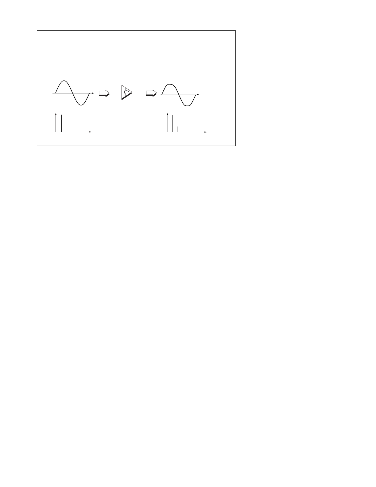
Linear devices impose magnitude and phase changes on input signals (Figure 1).
Any sinusoid appearing at the input will also appear at the output, and at the
same frequency. No new signals are created. Both active and passive nonlinear
devices can shift an input signal in frequency or add other frequency components, such as harmonic and spurious signals. Large input signals can drive
normally linear devices into compression or saturation, causing nonlinear
operation.
Figure 1. Linear versus Nonlinear Behavior
A * Sin 360 * f ( t – t )
A
t
o
°
Sin 360 * f * t
Time
Input Output
DUT
A
phase shift =
* 360 * f
t
o
f
1
°
Time
°
Frequency
Linear behavior:
°
input and output frequencies
are the same (no additional
frequencies created)
output frequency only
undergoes magnitude and
phase change
Nonlinear behavior:
f
1
Frequency
Time
f
1
output frequency may undergo
frequency shift (e.g. with mixers)
additional frequencies created
(harmonics, intermodulation)
Frequency
Page 3
3
For linear distortion-free transmission, the amplitude response of the device
under test (DUT) must be flat and the phase response must be linear over the
desired bandwidth. As an example, consider a square-wave signal rich in highfrequency components passing through a bandpass filter that passes selected
frequencies with little attenuation while attenuating frequencies outside of the
passband by varying amounts.
Even if the filter has linear phase performance, the out-of-band components of
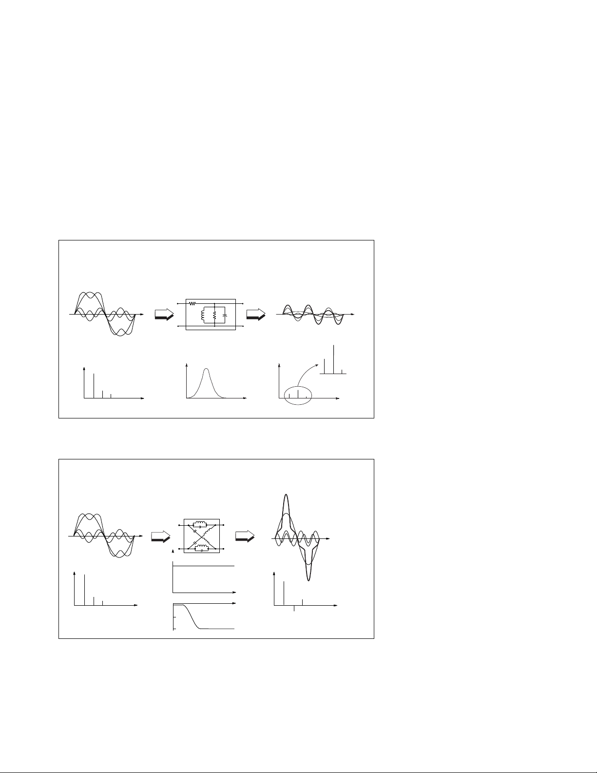
the square wave will be attenuated, leaving an output signal that, in this example, is more sinusoidal in nature (Figure 2).
If the same square-wave input signal is passed through a filter that only
inverts the phase of the third harmonic, but leaves the harmonic amplitudes
the same, the output will be more impulse-like in nature (Figure 3). While this
is true for the example filter, in general, the output waveform will appear with
arbitrary distortion, depending on the amplitude and phase nonlinearities.
Figure 2. Magnitude Variation with Frequency
Figure 3. Phase Variation with Frequency
F(t) = sin wt + 1/3 sin 3wt + 1/5 sin 5wt
Time
Linear
Network
Magnitude
Frequency
Frequency
F(t) = sin wt + 1/3 sin 3wt + 1/5 sin 5wt
Linear
Network
Time
Time
Frequency
Time
Magnitude
Frequency
°
Frequency
–180
–360
0
°
°
Frequency
Page 4
4
Figure 4. Nonlinear Induced Distortion
Nonlinear devices also introduce distortion (Figure 4). For example, if an amplifier is overdriven, the output signal clips because the amplifier is saturated.
The output signal is no longer a pure sinusoid, and harmonics are present at
multiples of the input frequency. Passive devices may also exhibit nonlinear
behavior at high power levels, a good example of which is an L-C filter that
uses inductors with magnetic cores. Magnetic materials often exhibit hysteresis
effects that are highly nonlinear.
Efficient transfer of power is another fundamental concern in communications
systems. In order to efficiently convey, transmit or receive RF power, devices
such as transmissions lines, antennas and amplifiers must present the proper
impedance match to the signal source. Impedance mismatches occur when the
real and imaginary parts of input and output impedances are not ideal
between two connecting devices.
Importance of Vector Measurements
Measuring both magnitude and phase of components is important for several
reasons. First, both measurements are required to fully characterize a linear
network and ensure distortion-free transmission. To design efficient matching
networks, complex impedance must be measured. Engineers developing models for computer-aided-engineering (CAE) circuit simulation programs require
magnitude and phase data for accurate models.
In addition, time-domain characterization requires magnitude and phase information in order to perform an inverse-fourier transform. Vector error correction, which improves measurement accuracy by removing the effects of inherent
measurement-system errors, requires both magnitude and phase data to build
an effective error model. Phase-measurement capability is very important even
for scalar measurements such as return loss, in order to achieve a high level of
accuracy (see Applying Error Correction to Network Analyzer Measurements,
Agilent application note 1287-3).
Nonlinear Networks
Saturation, crossover, intermodulation, and other
nonlinear effects can cause signal distortion
Time
Frequency
Time
Frequency
Page 5
5
The Basis of Incident and Reflected Power
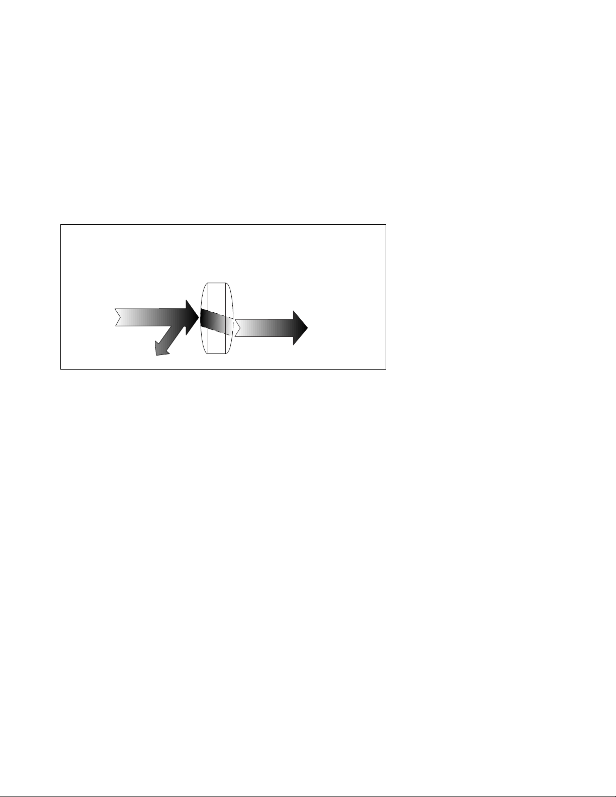
In its fundamental form, network analysis involves the measurement of incident, reflected, and transmitted waves that travel along transmission lines.
Using optical wavelengths as an analogy, when light strikes a clear lens (the
incident energy), some of the light is reflected from the lens surface, but most
of it continues through the lens (the transmitted energy) (Figure 5). If the lens
has mirrored surfaces, most of the light will be reflected and little or none will
pass through it.
While the wavelengths are different for RF and microwave signals, the principle is the same. Network analyzers accurately measure the incident, reflected,
and transmitted energy, e.g., the energy that is launched onto a transmission
line, reflected back down the transmission line toward the source (due to
impedence mismatch), and successfully transmitted to the terminating device
(such as an antenna).
Figure 5. Lightwave Analogy to High-Frequency Device Characterization
The Smith Chart
The amount of reflection that occurs when characterizing a device depends on
the impedance that the incident signal “sees.” Since any impedance can be represented with real and imaginary parts (R+jX or G+jB), they can be plotted on
a rectilinear grid known as the complex impedance plane. Unfortunately, an
open circuit (a common RF impedence) appears at infinity on the real axis,
and therefore cannot be shown.
The polar plot is useful because the entire impedance plane is covered. However,
instead of plotting impedance directly, the complex reflection coefficient is
displayed in vector form. The magnitude of the vector is the distance from the
center of the display, and phase is displayed as the angle of vector referenced
to a flat line from the center to the right-most edge. The drawback of polar
plots is that impedance values cannot be read directly from the display.
Lightwave Analogy
Incident
Transmitted
Reflected
Page 6

6
Since there is a one-to-one correspondence between complex impedance and
reflection coefficient, the positive real half of the complex impedance plane
can be mapped onto the polar display. The result is the Smith chart. All values
of reactance and all positive values of resistance from 0 to infinity fall within
the outer circle of the Smith chart (Figure 6).
On the Smith chart, loci of constant resistance appear as circles, while loci of
constant reactance appear as arcs. Impedances on the Smith chart are always
normalized to the characteristic impedance of the component or system of
interest, usually 50 ohms for RF and microwave systems and 75 ohms for
broadcast and cable-television systems. A perfect termination appears in the
center of the Smith chart.
Figure 6. Smith Chart Review
Power Transfer Conditions
A perfectly matched condition must exist at a connection between two devices
for maximum power transfer into a load, given a source resistance of R
S
and
a load resistance of R
L
. This condition occurs when RL= RS, and is true
whether the stimulus is a DC voltage source or a source of RF sine waves
(Figure 7).
When the source impedance is not purely resistive, maximum power transfer
occurs when the load impedance is equal to the complex conjugate of the
source impedance. This condition is met by reversing the sign of the imaginary
part of the impedance. For example, if R
S
= 0.6 + j 0.3, then the complex conju-
gate is R
S
* = 0.6 – j 0.3.
The need for efficient power transfer is one of the main reasons for the use of
transmission lines at higher frequencies. At very low frequencies (with much
larger wavelengths), a simple wire is adequate for conducting power. The
resistance of the wire is relatively low and has little effect on low-frequency
signals. The voltage and current are the same no matter where a measurement
is made on the wire.
+jX
+R
0
–jX
∞
0
Rectilinear impedance
plane
Smith chart maps
rectilinear impedance
plane onto polar plane
Z = 0
L
Γ
=
∞
1
Z = Zo
Γ
(short)
±180
Polar plane
L
=
0
O
o
+
180
–
o
90
.2
o
–90
Constant X
Z =
Γ
Smith chart
.8
.6
.4
Constant R
L
= 0
1
1.0
0
(open)
O
o
Page 7

7
At higher frequencies, wavelengths are comparable to or smaller than the
length of the conductors in a high-frequency circuit, and power transmission
can be thought of in terms of traveling waves. When the transmission line is
terminated in its characteristic impedance, maximum power is transferred to
the load. When the termination is not equal to the characteristic impedance,
that part of the signal that is not absorbed by the load is ref lected back to
the source.
If a transmission line is terminated in its characteristic impedance, no reflected
signal occurs since all of the transmitted power is absorbed by the load (Figure 8).
Looking at the envelope of the RF signal versus distance along the transmission
line shows no standing waves because without reflections, energy flows in only
one direction.
Figure 7. Power Transfer
Figure 8. Transmission Line Terminated with Z
0
R
S
R
L
1.2
1
0.8
0.6
0.4
0.2
Load Power (normalized)
0
0 1 2 3 4 5 6 7 8 9 10
RL / R
S
Maximum power is transferred
when R
= R
L
S
For complex impedances,
maximum power transfer occurs
when Z
= Z
* (conjugate match)
L
S
Zs = R + jX
Z
= Z
* = R – jX
s
L
Zo = characteristic impedance
of transmission line
o
V
inc
Zs = Z
V
power is absorbed in the load)
For reflection, a transmission line terminated in Zo
behaves like an infinitely long transmission line
Z
o
= 0 (all the incident
refl
Page 8

8
When the transmission line is terminated in a short circuit (which can sustain
no voltage and therefore dissipates zero power), a reflected wave is launched
back along the line toward the source (Figure 9). The reflected voltage wave
must be equal in magnitude to the incident voltage wave and be 180 degrees
out of phase with it at the plane of the load. The reflected and incident waves
are equal in magnitude but traveling in the opposite directions.
If the transmission line is terminated in an open-circuit condition (which can
sustain no current), the reflected current wave will be 180 degrees out of
phase with the incident current wave, while the reflected voltage wave will be
in phase with the incident voltage wave at the plane of the load. This guarantees that the current at the open will be zero. The reflected and incident current waves are equal in magnitude, but traveling in the opposite directions.
For both the short and open cases, a standing wave pattern is set up on the
transmission line. The voltage valleys will be zero and the voltage peaks will
be twice the incident voltage level.
If the transmission line is terminated with say a 25-ohm resistor, resulting in
a condition between full absorption and full reflection, part of the incident
power is absorbed and part is reflected. The amplitude of the reflected voltage
wave will be one-third that of the incident wave, and the two waves will be 180
degrees out of phase at the plane of the load. The valleys of the standing-wave
pattern will no longer be zero, and the peaks will be less than those of the
short and open cases. The ratio of the peaks to valleys will be 2:1.
The traditional way of determining RF impedance was to measure VSWR using
an RF probe/detector, a length of slotted transmission line, and a VSWR meter.
As the probe was moved along the transmission line, the relative position and
values of the peaks and valleys were noted on the meter. From these measurements, impedance could be derived. The procedure was repeated at different
frequencies. Modern network analyzers measure the incident and reflected
waves directly during a frequency sweep, and impedance results can be displayed in any number of formats (including VSWR).
Figure 9. Transmission Line Terminated with Short, Open
Zs = Z
V
inc
For reflection, a transmission line terminated in
a short or open reflects all power back to source
o
In phase (0 ) for open
V
refl
Out of phase (180 ) for short
o
o
Page 9

9
Network Analysis Terminology
Now that we understand the fundamentals of electromagnetic waves, we must
learn the common terms used for measuring them. Network analyzer terminology generally denotes measurements of the incident wave with the R or reference channel. The reflected wave is measured with the A channel, and the
transmitted wave is measured with the B channel (Figure 10). With the amplitude and phase information in these waves, it is possible to quantify the reflection and transmission characteristics of a DUT. The reflection and transmission
characteristics can be expressed as vector (magnitude and phase), scalar (magnitude only), or phase-only quantities. For example, return loss is a scalar
measurement of reflection, while impedance is a vector reflection measurement.
Ratioed measurements allow us to make reflection and transmission measurements that are independent of both absolute power and variations in source
power versus frequency. Ratioed reflection is often shown as A/R and ratioed
transmission as B/R, relating to the measurement channels in the instrument.
Figure 10. Common Terms for High-Frequency Device Characterization
The most general term for ratioed reflection is the complex reflection coeffi-
cient, Γ or gamma (Figure 11). The magnitude portion of Γ is called ρ or rho.
The reflection coefficient is the ratio of the reflected signal voltage level to the
incident signal voltage level. For example, a transmission line terminated in
its characteristic impedance Z
o
,will have all energy transferred to the load so
V
refl
= 0 and ρ = 0. When the impedance of the load, Z
L
is not equal to the char-
acteristic impedance, energy is reflected and ρ is greater than zero. When the
load impedance is equal to a short or open circuit, all energy is reflected and
ρ = 1. As a result, the range of possible values for ρ is 0 to 1.
Incident
R
Reflected
Transmitted
B
A
REFLECTION
Γ, ρ
A
=
R
Impedance,
Admittance
Return
Loss
R+jX,
G+jB
Gain / Loss
S-Parameters
S21,S12
SWR
S-Parameters
S11,S22
Reflected
Incident
Reflection
Coefficient
TRANSMISSION
Transmitted
Incident
Transmission
Coefficient
Τ,τ
B
=
R
Insertion
Phase
Group
Delay
Page 10

10
Figure 11. Reflection Parameters
Return loss is a way to express the reflection coefficient in logarithmic terms
(decibels). Return loss is the number of decibels that the reflected signal is
below the incident signal. Return loss is always expressed as a positive number
and varies between infinity for a load at the characteristic impedance and 0 dB
for an open or short circuit. Another common term used to express reflection
is voltage standing wave ratio (VSWR), which is defined as the maximum value
of the RF envelope over the minimum value of the RF envelope. It is related to
ρ as (1 + ρ)/(1 – ρ). VSWR ranges from 1 (no reflection) to infinity (full reflection).
The transmission coefficient is defined as the transmitted voltage divided by
the incident voltage (Figure 12). If the absolute value of the transmitted voltage is greater than the absolute value of the incident voltage, a DUT or system
is said to have gain. If the absolute value of the transmitted voltage is less than
the absolute value of the incident voltage, the DUT or system is said to have
attenuation or insertion loss. The phase portion of the transmission coefficient
is called insertion phase.
Reflection
Figure 12. Transmission Parameters
Coefficient
Γ
=
V
reflected
V
incident
−
Z
Z
O
L
Φ
=
Z
Z
+
O
L
=
ρ
Return loss = –20 log(ρ),
No reflection
(Z
= Zo)
L
0
∞ dB
1
ρ
Emax
Emin
ρ
RL
VSWR
=
Γ
Voltage Standing Wave Ratio
VSWR =
E
Emin
(Z
=
1 + ρ
1 – ρ
max
Full reflection
= open, short)
L
1
0 dB
∞
V
Incident
V
Transmitted
DUT
V
Transmitted
V
Trans
V
Inc
=
V
Incident
V
Trans
V
Inc
= 20 log τ
= τ∠φ
= –20 log τ
Transmission Coefficient = Τ
Insertion Loss (dB) = –20 Log
Gain (dB) = 20 Log
Page 11

11
Direct examination of insertion phase usually does not provide useful information. This is because the insertion phase has a large (negative) slope with
respect to frequency due to the electrical length of the DUT. The slope is proportional to the length of the DUT. Since it is only deviation from linear phase
that causes distortion in communications systems, it is desirable to remove the
linear portion of the phase response to analyze the remaining nonlinear portion. This can be done by using the electrical delay feature of a network analyzer to mathematically cancel the average electrical length of the DUT. The result
is a high-resolution display of phase distortion or deviation from linear phase
(Figure 13).
Figure 13. Deviation from Linear Phase
Measuring Group Delay
Another useful measure of phase distortion is group delay (Figure 14). This
parameter is a measure of the transit time of a signal through a DUT versus
frequency. Group delay can be calculated by differentiating the DUT’s phase
response versus frequency. It reduces the linear portion of the phase response
to a constant value, and transforms the deviations from linear phase into deviations from constant group delay, (which causes phase distortion in communications systems). The average delay represents the average signal transit time
through a DUT.
Figure 14. What is group Delay?
Use electrical delay to remove
linear portion of phase response
RF filter response
o
Phase 45 /Div
Frequency
Linear electrical
length added
(Electrical delay function)
+
Frequency
yields
Deviation from
linear phase
Frequency
o
Phase 1 /Div
Low resolution High resolution
t
Frequency
φ
Phase
∆φ
Group Delay (t )
in radians
φ
in radians/sec
ω
in degrees
φ
in Hz
f
ω
∆ω
−δ φ
=
g
d ω
d φ
−1
=
o
*
d
360
(
ω
)
f
=
π
2
g
Group
Delay
t
o
f
Group Delay
Average Delay
Frequency
Deviation from constant group
delay indicates distortion
Average delay indicates transit time
Page 12

12
Depending on the device, both deviation from linear phase and group delay
may be measured, since both can be important. Specifying a maximum peakto-peak phase ripple in a device may not be sufficient to completely characterize it, since the slope of the phase ripple depends on the number of ripples
that occur per unit of frequency. Group delay takes this into account because
it is the differentiated phase response. Group delay is often a more easily
interpreted indication of phase distortion (Figure 15).
Figure 15. Why measure Group Delay?
Network Characterization
In order to completely characterize an unknown linear two-port device, we
must make measurements under various conditions and compute a set of
parameters. These parameters can be used to completely describe the electrical behavior of our device (or network), even under source and load conditions
other than when we made our measurements. Low-frequency device or network characterization is usually based on measurement of H, Y, and Z parameters. To do this, the total voltage and current at the input or output ports of a
device or nodes of a network must be measured. Furthermore, measurements
must be made with open-circuit and short-circuit conditions.
Since it is difficult to measure total current or voltage at higher frequencies,
S-parameters are generally measured instead (Figure 16). These parameters
relate to familiar measurements such as gain, loss, and reflection coefficient.
They are relatively simple to measure, and do not require connection of undesirable loads to the DUT. The measured S-parameters of multiple devices can
be cascaded to predict overall system performance. S-parameters are readily
used in both linear and nonlinear CAE circuit simulation tools, and H, Y, and
Z parameters can be derived from S-parameters when necessary.
The number of S-parameters for a given device is equal to the square of the
number of ports. For example, a two-port device has four S-parameters. The
numbering convention for S-parameters is that the first number following the
S is the port at which energy emerges, and the second number is the port at
which energy enters. So S
21
is a measure of power emerging from Port 2 as a
result of applying an RF stimulus to Port 1. When the numbers are the same
(e.g. S
11
), a reflection measurement is indicated.
Phase
Group
Delay
−dφ
dω
f
f
Phase
Group
Delay
−dφ
f
dω
f
Same peak-to-peak phase ripple can result in different group delay
Page 13

13
Forward S-parameters are determined by measuring the magnitude and phase
of the incident, reflected, and transmitted signals when the output is terminated
in a load that is precisely equal to the characteristic impedance of the test
system. In the case of a simple two-port network, S
11
is equivalent to the input
complex reflection coefficient or impedance of the DUT, while S
21
is the forward complex transmission coefficient. By placing the source at the output
port of the DUT and terminating the input port in a perfect load, it is possible
to measure the other two (reverse) S-parameters. Parameter S
22
is equivalent
to the output complex reflection coefficient or output impedance of the DUT
while S
12
is the reverse complex transmission coefficient (Figure 17).
Suggested Reading
Exploring the Architectures of Network Analyzers, Agilent
application note 1287-2.
Applying Error Correction to Network Analyzer Measurements,
Agilent application note 1287-3.
Network Analyzer Measurements: Filter and Amplifier Examples,
Agilent application note 1287-4.
H,Y, and Z parameters
Figure 16. Limitations of H, Y, and Z Parameters (Why Use S-parameters?)
Figure 17. Measuring S-Parameters
Hard to measure total voltage and current
at device ports at high frequencies
Active devices may oscillate or self-destruct with shorts or opens
S-parameters
Relate to familiar measurements
(gain, loss, reflection coefficient, etc.)
Relatively easy to measure
Can cascade S-parameters of multiple
devices to predict system performance
Analytically convenient
Incident
a
1
S
11
Reflected
b
1
Transmitted
CAD programs
Flow-graph analysis
Can compute H, Y, or Z parameters from S-parameters if desired
Forward
Reflected
=
S
11
Incident
Transmitted
=
S
21
Incident
Incident Transmitted
a
1
S
11
Reflected
b
1
b
1
=
a
=
2
a
1
b
2
=
a
=
2
a
1
S
21
DUT
0
=
S
0
22
=
S
12
S
DUT
Port 1
b
=
S
1
11
b
=
S
21
2
a
2
Reflected
Incident
Transmitted
Incident
21
Port 2
S
a
a1+
b
2
=
12
+
1
0
=
=
Transmitted
S
12
S
22
Z
Load
b
a
b
a
S
22
Reflected
Incident
a
2
a
2
0
2
a
1
2
1
a
1
2
b
2
a
2
0
=
0
=
a
=
0
Z
0
Load
1
DUT
S
b
1
12
Reflected
IncidentTransmitted
b
S
2
22
Reverse
a
2
Page 14

Agilent Technologies’ Test and Measurement
Support, Services, and Assistance
Agilent Technologies aims to maximize
the value you receive, while minimizing
your risk and problems. We strive to
ensure that you get the test and measurement capabilities you paid for and obtain
the support you need. Our extensive support resources and services can help you
choose the right Agilent products for your
applications and apply them successfully.
Every instrument and system we sell has
a global warranty. Support is available
for at least five years beyond the production life of the product. Two concepts
underlie Agilent’s overall support policy:
“Our Promise” and “Your Advantage.”
Our Promise
“Our Promise” means your Agilent test
and measurement equipment will meet its
advertised performance and functionality.
When you are choosing new equipment,
we will help you with product information, including realistic performance specifications and practical recommendations
from experienced test engineers. When
you use Agilent equipment, we can verify
that it works properly, help with product
operation, and provide basic measurement
assistance for the use of specified capabilities, at no extra cost upon request. Many
self-help tools are available.
Your Advantage
“Your Advantage” means that Agilent
offers a wide range of additional expert
test and measurement services, which you
can purchase according to your unique
technical and business needs. Solve problems efficiently and gain a competitive edge
by contracting with us for calibration, extracost upgrades, out-of-warranty repairs, and
on-site education and training, as well
as design, system integration, project management, and other professional services.
Experienced Agilent engineers and technicians worldwide can help you maximize
your productivity, optimize the return on
investment of your Agilent instruments and
systems, and obtain dependable measurement accuracy for the life of those products.
By internet, phone, or fax, get assistance
with all your test and measurement needs.
Online Assistance
www.agilent.com/find/assist
Phone or Fax
United States:
(tel) 1 800 452 4844
Canada:
(tel) 1 877 894 4414
(fax) (905) 206 4120
Europe:
(tel) (31 20) 547 2323
(fax) (31 20) 547 2390
Japan:
(tel) (81) 426 56 7832
(fax) (81) 426 56 7840
Latin America:
(tel) (305) 269 7500
(fax) (305) 269 7599
Australia:
(tel) 1 800 629 485
(fax) (61 3) 9272 0749
New Zealand:
(tel) 0 800 738 378
(fax) (64 4) 495 8950
Asia Pacific:
(tel) (852) 3197 7777
(fax) (852) 2506 9284
Product specifications and descriptions in this
document subject to change without notice.
Copyright © 1997, 2000 Agilent Technologies
Printed in U.S.A. 8/00
5965-7707E
 Loading...