

Page 1
Low Input Current, High Gain
Optocouplers
Technical Data
6N139 6N138
HCPL-0701 HCPL-0700
HCNW139 HCNW138
Features
• High Current Transfer Ratio
– 2000% Typical (4500%
Typical for HCNW139/138)
• Low Input Current
Requirements – 0.5 mA
• TTL Compatible Output –
0.1 V VOL Typical
• Performance Guaranteed
over Temperature 0°C
to 70°C
• Base Access Allows Gain
Bandwidth Adjustment
• High Output Current –
60 mA
• Safety Approval
UL Recognized – 3750 V rms
for 1 Minute and 5000 V rms*
for 1 Minute per UL 1577
CSA Approved
IEC/EN/DIN EN 60747-5-2
Approved with V
V peak for HCNW139 and
HCNW138
• Available in 8-Pin DIP or
SOIC-8 Footprint or
Widebody Package
• MIL-PRF-38534 Hermetic
Version Available (HCPL5700/1)
IORM
= 1414
Applications
• Ground Isolate Most Logic
Families – TTL/TTL, CMOS/
TTL, CMOS/CMOS, LSTTL/
TTL, CMOS/LSTTL
• Low Input Current Line
Receiver
• High Voltage Insulation
(HCNW139/138)
• EIA RS-232C Line Receiver
• Telephone Ring Detector
• 117 V ac Line Voltage Status
Indicator – Low Input Power
Dissipation
• Low Power Systems –
Ground Isolation
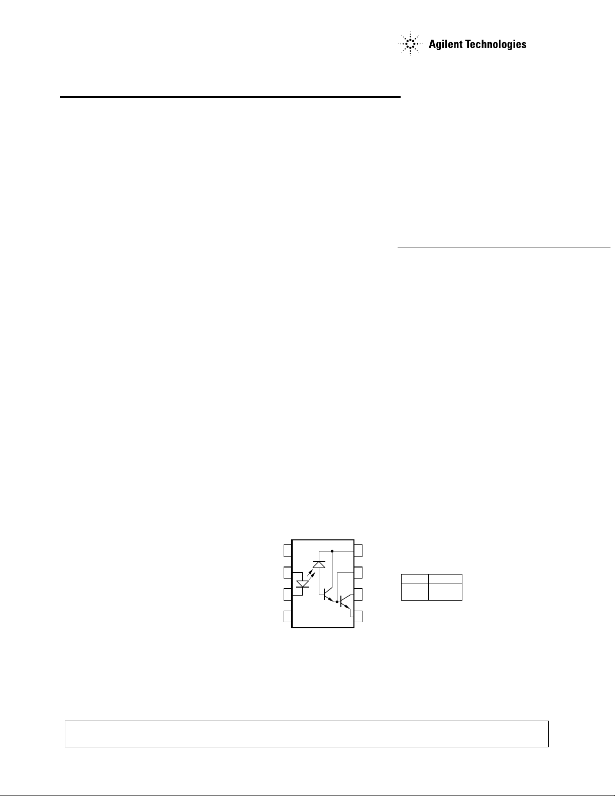
Functional Diagram
NC
ANODE
CATHODE
NC
1
2
3
4
8
V
7
V
6
V
5
GND
Description
These high gain series couplers
use a Light Emitting Diode and an
integrated high gain photodetector to provide extremely high
current transfer ratio between
input and output. Separate pins
for the photodiode and output
stage result in TTL compatible
saturation voltages and high
speed operation. Where desired
the VCC and VO terminals may be
tied together to achieve conventional photodarlington operation.
A base access terminal allows a
gain bandwidth adjustment to be
made.
CC
B
O
TRUTH TABLE
LED
ON
OFF
V
LOW
HIGH
O
*5000 V rms/1 minute rating is for HCNW139/138 and Option 020 (6N139/138) products only.
A 0.1 µF bypass capacitor connected between pins 8 and 5 is recommended.
CAUTION: It is advised that normal static precautions be taken in handling and assembly of this component to
prevent damage and/or degradation which may be induced by ESD.
Page 2
2
The 6N139, HCPL-0701, and
CNW139 are for use in CMOS,
LSTTL or other low power applications. A 400% minimum current
transfer ratio is guaranteed over
0 to 70°C operating range for only
0.5 mA of LED current.
(1 TTL Unit load ). A 300%
minimum CTR enables operation
with 1 TTL Load using a 2.2 kΩ
pull-up resistor.
Selection for lower input current
down to 250 µA is available upon
request.
The SOIC-8 does not require
“through holes” in a PCB. This
package occupies approximately
one-third the footprint area of the
standard dual-in-line package.
The lead profile is designed to be
compatible with standard surface
mount processes.
The 6N138, HCPL-0700, and
HCNW138 are designed for use
mainly in TTL applications.
Current Transfer Ratio (CTR) is
300% minimum over 0 to 70°C
for an LED current of 1.6 mA
The HCPL-0701 and HCPL-0700
are surface mount devices
packaged in an industry standard
SOIC-8 footprint.
The HCNW139 and HCNW138
are packaged in a widebody
encapsulation that provides creep-
age and clearance dimensions
suitable for safety approval by
regulatory agencies worldwide.
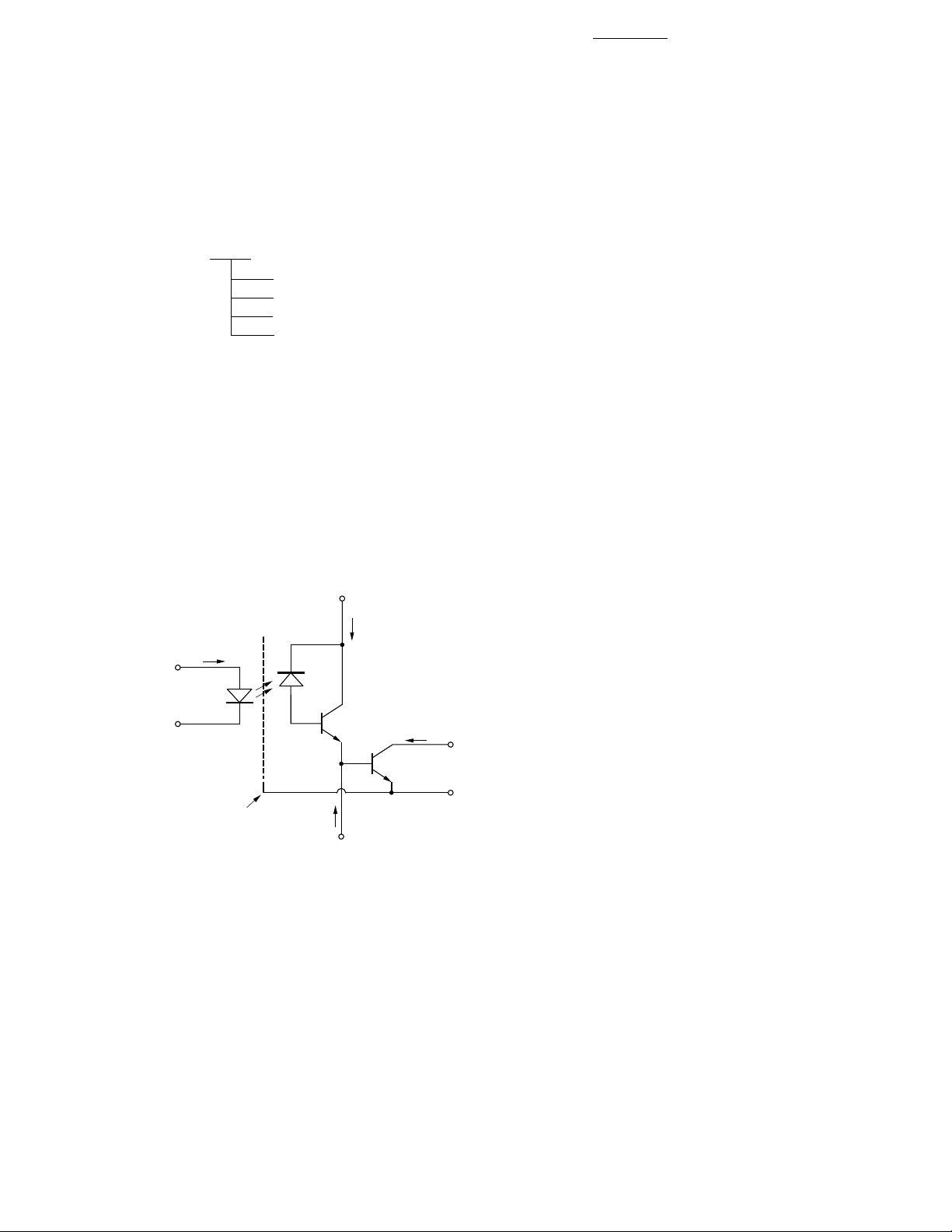
Selection Guide
Widebody
8-Pin DIP Package Hermetic
(300 Mil) Small Outline SO-8 (400 mil) Single and
Dual Single Dual Minimum Absolute Dual
Single Channel Channel Channel Single Input ON Maxi- Channel
Channel Package Package Package Channel Current Minimum mum Packages
Package HCPL- HCPL- HCPL- Package (I
4731
[1]
[1]
[1]
0701 0731 HCNW139 0.5 mA 400% 18 V
0700 0730 HCNW138 1.6 mA 300% 7 V
070A
[1]
073A
[1]
6N139 2731
6N138 2730
HCPL-4701
[1]
) CTR V
F
40 µA 800% 18 V
0.5 mA 300% 20 V 5701
CC
HCPL-
[1]
[1]
5700
[1]
5731
[1]
5730
Note:
1. Technical data are on separate Agilent publications.
Page 3
3
Ordering Information
Specify Part Number followed by Option Number (if desired).
Example:
6N139#XXXX
020 = 5000 V rms/1 Minute UL Rating Option*
300 = Gull Wing Surface Mount Option†
500 = Tape and Reel Packaging Option
XXXE = Lead Free Option
Option data sheets available. Contact your Agilent sales representative or authorized distributor for
information.
*For 6N139 and 6N138 only.
†Gull wing surface mount option applies to through hole parts only.
Remarks: The notation “#” is used for existing products, while (new) products launched since 15th July
2001 and lead free option will use “-”
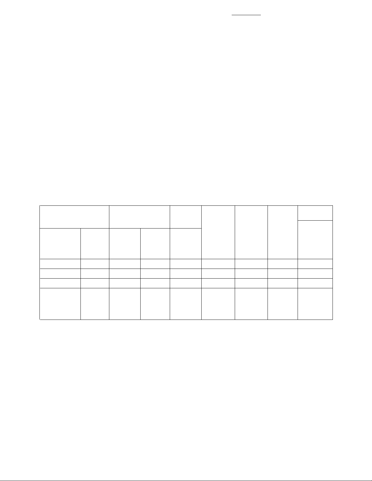
Schematic
2
ANODE
+
V
F
CATHODE
–
3
V
CC
8
I
CC
I
F
I
O
6
V
O
5
GND
SHIELD
I
B
7
V
B
Page 4
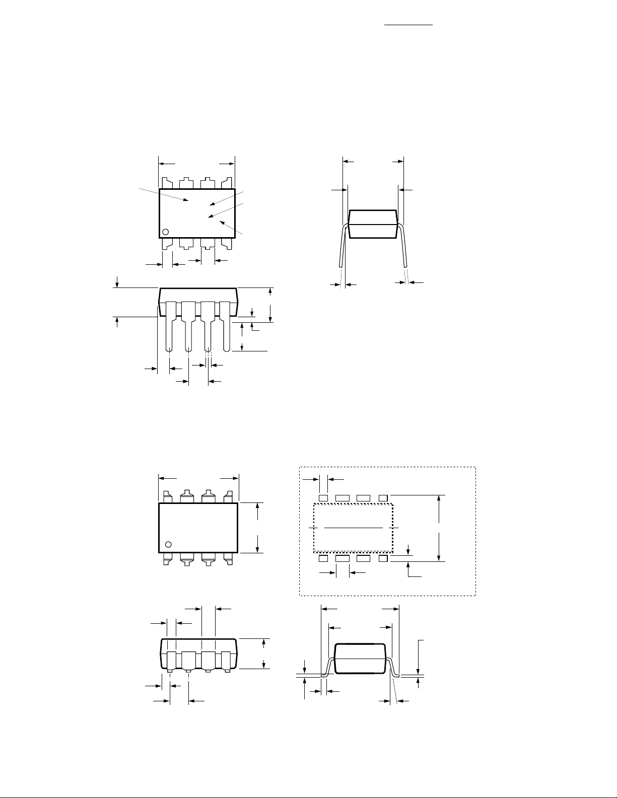
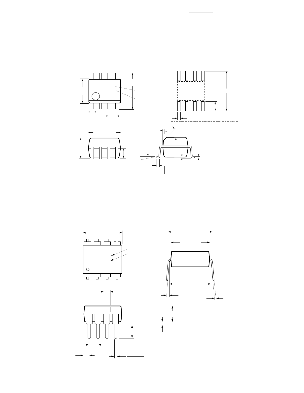
Package Outline Drawings
8-Pin DIP Package (6N139/6N138)**
4
7.62 ± 0.25
(0.300 ± 0.010)
6.35 ± 0.25
(0.250 ± 0.010)
5° TYP.
0.254
(0.010
TYPE NUMBER
1.19 (0.047) MAX.
3.56 ± 0.13
(0.140 ± 0.005)
1.080 ± 0.320
(0.043 ± 0.013)
9.65 ± 0.25
(0.380 ± 0.010)
A XXXXZ
YYWW
5678
OPTION CODE*
DATE CODE
UR
UL
4321
RECOGNITION
1.78 (0.070) MAX.
4.70 (0.185) MAX.
2.92 (0.115) MIN.
0.65 (0.025) MAX.
2.54 ± 0.25
(0.100 ± 0.010)
0.51 (0.020) MIN.
DIMENSIONS IN MILLIMETERS AND (INCHES).
* MARKING CODE LETTER FOR OPTION NUMBERS
"L" = OPTION 020
OPTION NUMBERS 300 AND 500 NOT MARKED.
NOTE: FLOATING LEAD PROTRUSION IS 0.25 mm (10 mils) MAX.
**JEDEC Registered Data.
8-Pin DIP Package with Gull Wing Surface Mount Option 300 (6N139/6N138)
+ 0.076
- 0.051
+ 0.003)
- 0.002)
1.19
(0.047)
MAX.
1.080 ± 0.320
(0.043 ± 0.013)
LAND PATTERN RECOMMENDATION
9.65 ± 0.25
(0.380 ± 0.010)
6
7
8
1
2
2.54
(0.100)
BSC
DIMENSIONS IN MILLIMETERS (INCHES).
LEAD COPLANARITY = 0.10 mm (0.004 INCHES).
NOTE: FLOATING LEAD PROTRUSION IS 0.25 mm (10 mils) MAX.
5
6.350 ± 0.25
(0.250 ± 0.010)
3
4
1.27 (0.050)
1.780
(0.070)
MAX.
3.56 ± 0.13
(0.140 ± 0.005)
0.635 ± 0.130
(0.025 ± 0.005)
(0.380 ± 0.010)
(0.300 ± 0.010)
0.635 ± 0.25
(0.025 ± 0.010)
1.016 (0.040)
9.65 ± 0.25
7.62 ± 0.25
10.9 (0.430)
2.0 (0.080)
0.254
(0.010
12° NOM.
+ 0.076
- 0.051
+ 0.003)
- 0.002)
Page 5
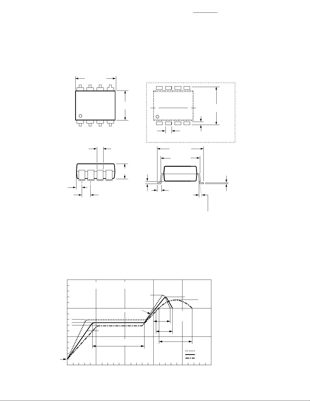
5
Small Outline SO-8 Package (HCPL-0701/HCPL-0700)
8765
3.937 ± 0.127
(0.155 ± 0.005)
PIN ONE
0.406 ± 0.076
(0.016 ± 0.003)
3.175 ± 0.127
(0.125 ± 0.005)
TOTAL PACKAGE LENGTH (INCLUSIVE OF MOLD FLASH)
*
5.207 ± 0.254 (0.205 ± 0.010)
DIMENSIONS IN MILLIMETERS (INCHES).
LEAD COPLANARITY = 0.10 mm (0.004 INCHES) MAX.
NOTE: FLOATING LEAD PROTRUSION IS 0.15 mm (6 mils) MAX.
XXX
YWW
*
5.080 ± 0.127
(0.200 ± 0.005)
4321
1.270
(0.050)
5.994 ± 0.203
(0.236 ± 0.008)
TYPE NUMBER
(LAST 3 DIGITS)
DATE CODE
BSC
1.524
(0.060)
7°
0 ~ 7°
LAND PATTERN RECOMMENDATION
0.64 (0.025)
0.432
45° X
(0.017)
(0.009 ± 0.001)
0.203 ± 0.102
(0.008 ± 0.004)
0.305
MIN.
(0.012)
7.49 (0.295)
1.9 (0.075)
0.228 ± 0.025
8-Pin Widebody DIP Package (HCNW139/HCNW138)
11.15 ± 0.15
(0.442 ± 0.006)
6
5
TYPE NUMBER
DATE CODE
3
4
1.55
(0.061)
MAX.
3.10 (0.122)
3.90 (0.154)
0.40 (0.016)
0.56 (0.022)
2.54 (0.100)
TYP.
1.78 ± 0.15
(0.070 ± 0.006)
7
8
HCNWXXXX
1
2
A
YYWW
11.00
MAX.
(0.433)
9.00 ± 0.15
(0.354 ± 0.006)
10.16 (0.400)
TYP.
7° TYP.
5.10
MAX.
(0.201)
0.51 (0.021) MIN.
DIMENSIONS IN MILLIMETERS (INCHES).
NOTE: FLOATING LEAD PROTRUSION IS 0.25 mm (10 mils) MAX.
0.254
(0.010
+ 0.076
- 0.0051
+ 0.003)
- 0.002)
Page 6
6
8-Pin Widebody DIP Package with Gull Wing Surface Mount Option 300 (HCNW139/HCNW138)
1.78 ± 0.15
(0.070 ± 0.006)
11.15 ± 0.15
(0.442 ± 0.006)
6
3
2.54
(0.100)
BSC
5
(0.354 ± 0.006)
4
1.55
(0.061)
MAX.
9.00 ± 0.15
4.00
MAX.
(0.158)
(0.030 ± 0.010)
7
8
1
2
DIMENSIONS IN MILLIMETERS (INCHES).
LEAD COPLANARITY = 0.10 mm (0.004 INCHES).
NOTE: FLOATING LEAD PROTRUSION IS 0.25 mm (10 mils) MAX.
LAND PATTERN RECOMMENDATION
1.3
(0.051)
0.75 ± 0.25
(0.039 ± 0.006)
12.30 ± 0.30
(0.484 ± 0.012)
11.00
MAX.
(0.433)
1.00 ± 0.15
2.29
(0.09)
7° NOM.
13.56
(0.534)
0.254
(0.010
+ 0.076
- 0.0051
+ 0.003)
- 0.002)
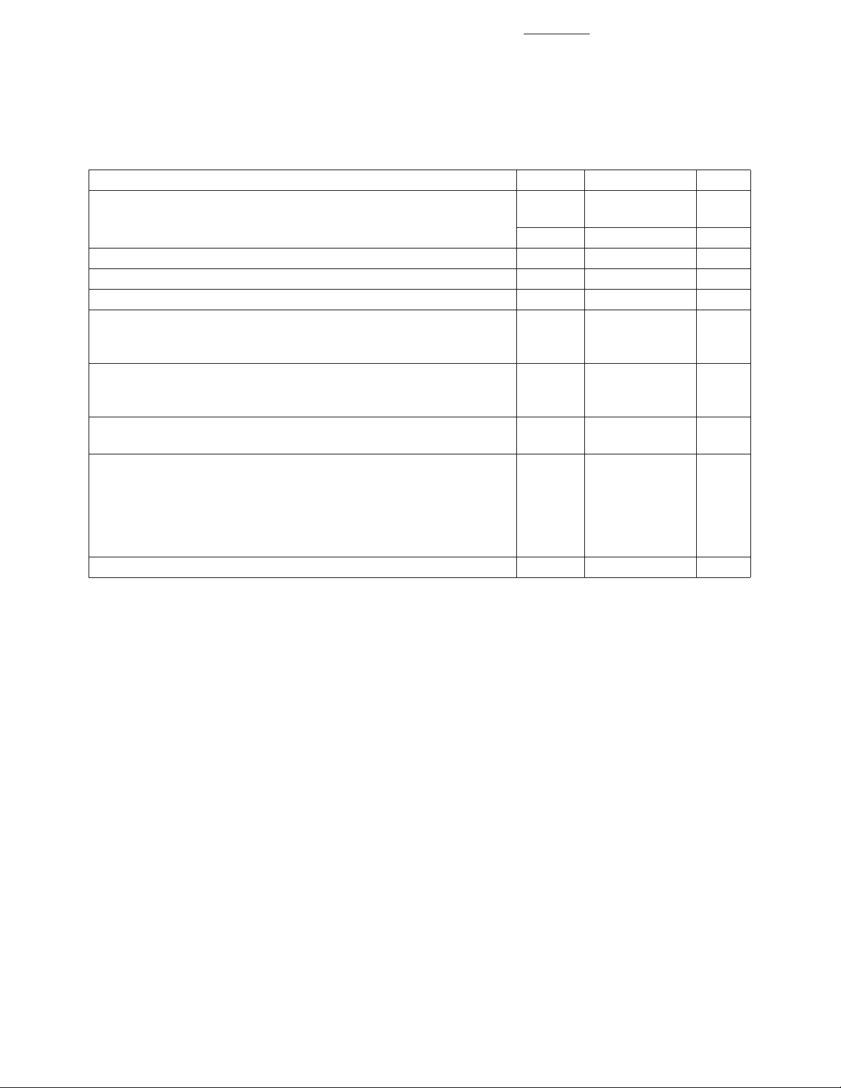
Solder Reflow Temperature Profile
300
PREHEATING RATE 3°C + 1°C/–0.5°C/SEC.
REFLOW HEATING RATE 2.5°C ± 0.5°C/SEC.
ROOM
TEMPERATURE
200
160°C
150°C
140°C
100
TEMPERATURE (°C)
0
0
3°C + 1°C/–0.5°C
50 150100 200 250
2.5°C ± 0.5°C/SEC.
PREHEATING TIME
150°C, 90 + 30 SEC.
TIME (SECONDS)
PEAK
TEMP.
245°C
30
SEC.
SEC.
30
SOLDERING
TIME
200°C
50 SEC.
PEAK
TEMP.
240°C
PEAK
TEMP.
230°C
TIGHT
TYPICAL
LOOSE
Page 7

Pb-Free IR Profile
T
p
217 °C
T
L
T
smax
T
smin
TEMPERATURE
150 - 200 °C
3 °C/SEC. MAX.
60 to 180 SEC.
RAMP-UP
t
s
PREHEAT
260 +0/-5 °C
TIME WITHIN 5 °C of ACTUAL
PEAK TEMPERATURE
t
p
15 SEC.
RAMP-DOWN
6 °C/SEC. MAX.
t
L
60 to 150 SEC.
7
25
NOTES:
THE TIME FROM 25 °C to PEAK TEMPERATURE = 8 MINUTES MAX.
T
= 200 °C, T
smax
Regulatory Information
The 6N139/138, HCNW139/138,
and HCPL-0701/0700 have been
approved by the following
organizations:
t 25 °C to PEAK
= 150 °C
smin
TIME
UL
Recognized under UL 1577,
Component Recognition Program,
File E55361.
CSA
Approved under CSA Component
IEC/EN/DIN EN 60747-5-2
Approved under
IEC 60747-5-2:1997 + A1:2002
EN 60747-5-2:2001 + A1:2002
DIN EN 60747-5-2 (VDE 0884
Teil 2):2003-01
(HCNW139/138 only)
Acceptance Notice #5, File CA
88324.
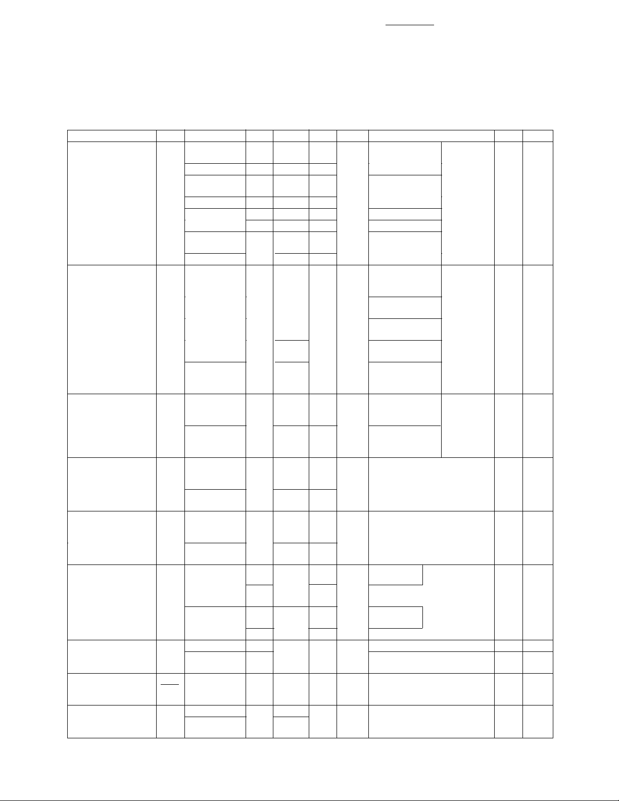
Insulation and Safety Related Specifications
8-Pin DIP Widebody
(300 Mil) SO-8 (400 Mil)
Parameter Symbol Value Value Value Units Conditions
Minimum External L(101) 7.1 4.9 9.6 mm Measured from input terminals
Air Gap (External to output terminals, shortest
Clearance) distance through air.
Minimum External L(102) 7.4 4.8 10.0 mm Measured from input terminals
Tracking (External to output terminals, shortest
Creepage) distance path along body.
Minimum Internal 0.08 0.08 1.0 mm Through insulation distance,
Plastic Gap conductor to conductor, usually
(Internal Clearance) the direct distance between the
photoemitter and photodetector
inside the optocoupler cavity.
Minimum Internal NA NA 4.0 mm Measured from input terminals
Tracking (Internal to output terminals, along
Creepage) internal cavity.
Tracking Resistance CTI 200 200 200 Volts DIN IEC 112/VDE 0303 Part 1
(Comparative
Tracking Index)
Isolation Group IIIa IIIa IIIa Material Group
(DIN VDE 0110, 1/89, Table 1)
Option 300 - surface mount classification is Class A in accordance with CECC 00802.
Page 8
8
IEC/EN/DIN EN 60747-5-2 Insulation Related Characteristics (HCNW139 and HCNW138)
Description Symbol Characteristic Units
Installation Classification per DIN VDE 0110/1.89, Table 1
for rated mains voltage ≤ 600 V rms I-IV
for rated mains voltage ≤ 1000 V rms I-III
Climatic Classification 55/100/21
Pollution Degree (DIN VDE 0110/1.89) 2
Maximum Working Insulation Voltage V
Input to Output Test Voltage, Method b*
VPR = 1.875 x V
, 100% Production Test with tP = 1 sec, V
IORM
Partial Discharge < 5 pC
Input to Output Test Voltage, Method a*
VPR = 1.5 x V
, Type and Sample Test, V
IORM
tP = 60 sec, Partial Discharge < 5 pC
Highest Allowable Overvoltage*
(Transient Overvoltage, t
= 10 sec) V
ini
Safety Limiting Values
(Maximum values allowed in the event of a failure,
also see Figure 11, Thermal Derating curve.)
Case Temperature T
Current (Input Current IF, PS = 0) I
Output Power P
S,INPUT
S,OUTPUT
Insulation Resistance at TS, VIO = 500 V R
IORM
PR
PR
IOTM
S
S
1414 V peak
2652 V peak
2121 V peak
8000 V peak
175 °C
400 mA
700 mW
9
> 10
Ω
*Refer to the front of the optocoupler section of the current catalog, under Product Safety Regulations section, IEC/EN/DIN EN
60747-5-2, for a detailed description.
Note: Isolation characteristics are guaranteed only within the safety maximum ratings which must be ensured by protective circuits in
application.
Page 9

Absolute Maximum Ratings* (No Derating Required up to 85°C)
Parameter Symbol Min. Max. Units
Storage Temperature T
Operating Temperature** T
Average Forward Input Current I
Peak Forward Input Current I
(50% Duty Cycle, 1 ms Pulse Width)
Peak Transient Input Current I
(<1 µs Pulse Width, 300 pps)
Reverse Input Voltage V
HCNW139/138 3 V
Input Power Dissipation P
Output Current (Pin 6) I
Emitter Base Reverse Voltage (Pin 5-7) V
S
A
F(AVG)
FPK
F(TRAN)
R
I
O
EB
9
-55 125 °C
-40 85 °C
20 mA
40 mA
1.0 A
5V
35 mW
60 mA
0.5 V
Supply Voltage and Output Voltage V
CC
-0.5 18 V
(6N139, HCPL-0701, HCNW139)
Supply Voltage and Output Voltage V
CC
-0.5 7 V
(6N138, HCPL-0700, HCNW138)
Output Power Dissipation P
Total Power Dissipation P
O
T
100 mW
135 mW
Lead Solder Temperature (for Through Hole Devices) 260°C for 10 sec., 1.6 mm below seating plane
HCNW139/138 260°C for 10 sec., up to seating plane
Reflow Temperature Profile See Package Outline Drawings section
(for SOIC-8 and Option #300)
*JEDEC Registered Data for 6N139 and 6N138.
**0°C to 70°C on JEDEC Registration.
Recommended Operating Conditions
Parameter Symbol Min. Max. Units
Power Supply Voltage V
Forward Input Current (ON) I
Forward Input Voltage (OFF) V
F(ON)
F(OFF)
Operating Temperature T
CC
A
4.5 18 V
0.5 12.0 mA
0 0.8 V
070°C
Page 10
10
Electrical Specifications
0°C ≤ TA ≤ 70°C, 4.5 V ≤ VCC ≤ 18 V, 0.5 mA ≤ I
specified. All Typicals at TA = 25°C. See Note 7.
Parameter Sym. Device Min. Typ.** Max. Units Test Conditions Fig. Note
Current Transfer CTR 6N139 400* 2000 5000 % IF = 0.5 mA V
Ratio HCPL-0701 VO = 0.4 V 4
HCNW139 400 4500
6N139 500* 1600 2600 IF = 1.6 mA
HCPL-0701
HCNW139 500 3000
300 1600 IF = 5.0 mA
200 850 IF = 12 mA
6N138 300* 1600 2600 IF = 1.6 mA
HCPL-0700
HCNW138 1500
Logic Low Output V
OL
6N139 0.1 0.4 V IF = 0.5 mA, V
Voltage HCPL-0701 IO = 2 mA
HCNW139
6N138 0.1 IF = 1.6 mA,
HCPL-0700 IO = 4.8 mA
HCNW138
Logic High I
OH
6N139 0.05 100 µAVO = V
Output Current HCPL-0701
HCNW139
6N138 0.1 250 VO = V
HCPL-0700
HCNW138
Logic Low Supply I
6N138/139 0.4 1.5 mA IF = 1.6 mA, VO = Open, 10 2
CCL
Current HCPL-0701/ V
0700
HCNW139 0.5 2
HCNW138
Logic High I
6N138/139 0.01 10 µAIF = 0 mA, VO = Open, 2
CCH
Supply Current HCPL-0701/ V
0700
HCNW139 1
HCNW138
Input Forward V
6N138 1.25 1.40 1.7* V TA = 25°CIF = 1.6 mA 4, 8
F
Voltage 6N139
HCPL-0701 1.75
HCPL-0700
HCNW139 1.0 1.45 1.85 TA = 25°C
HCNW138
0.95 1.95
Input Reverse BVR 5.0* V IR = 10 µA, TA = 25°C
Breakdown
Voltage
Temperature ∆V
Coefficient of ∆T
HCNW139 3.0 IR = 100 µA, TA = 25°C
HCNW138
F
A
Forward Voltage
Input C
IN
Capacitance HCNW139 90
HCNW138
*JEDEC Registered Data for 6N139 and 6N138.
**All typical values at T
= 25°C and V
A
= 5 V, unless otherwise noted.
CC
≤ 12 mA, 0 V ≤ V
F(ON)
≤ 0.8 V, unless otherwise
F(OFF)
CC
CC
= 4.5 2, 3 1, 2,
= 4.5 1 2
IF = 1.6 mA,
IO = 8 mA
IF = 5.0 mA,
IO = 15 mA
0.2 IF = 12 mA,
IO = 24 mA
= 18 V IF = 0 mA 2
CC
= 7 V
CC
= 18 V
CC
= 18 V
CC
-1.8 mV/°CIF = 1.6 mA 8
60 pF f = 1 MHz, VF = 0 V
Page 11

11
Switching Specifications (AC)
Over recommended operating conditions (TA = 0 to 70° C), VCC = 5 V, unless otherwise specified.
Parameter Sym. Device Min. Typ.** Max. Units Test Conditions Fig. Note
TA =25°C
Propagation t
PHL
Delay Time HCPL-0701 Rl = 4.7 kΩ 7, 9,
to Logic Low HCNW139 12
at Output
Propagation t
PLH
Delay Time HCPL-0701 Rl = 4.7 kΩ 7, 9,
to Logic High HCNW139 115 12
at Output
Common Mode |CMH| 1000 10000 V/µsIF = 0 mA, 13 5, 6
Transient TA = 25° C
Immunity at Rl = 2.2 kΩ
Logic High |VCM| = 10
Output Vp-p
Common Mode |CML| 1000 10000 V/µsIF = 1.6 mA, 13 5, 6
Transient TA = 25° C
Immunity at Rl = 2.2 kΩ
Logic Low |VCM| = 10
Output Vp-p
*JEDEC Registered Data for 6N139 and 6N138.
**All typical values at T
= 25°C and VCC = 5 V, unless otherwise noted.
A
6N139 5 25* 30 µsI
6N139 0.2 1* 2 µsI
= 0.5 mA, 5, 6, 2, 4
F
= 12 mA,
F
HCPL-0701 Rl = 270 Ω
HCNW139 11
6N138 1.6 10* 15 µsI
= 1.6 mA,
F
HCPL-0700 Rl = 2.2 kΩ
HCNW138 11
6N139 18 60* 90 µsI
6N139 2 7* 10 µsI
= 0.5 mA, 5, 6, 2, 4
F
= 12 mA,
F
HCPL-0701 Rl = 270 Ω
HCNW139 11
6N138 10 35* 50 µsI
= 1.6 mA,
F
HCPL-0700 Rl = 2.2 kΩ
HCNW138 70
Page 12

12
Package Characteristics
Parameter Sym. Min. Typ.** Max. Units Test Conditions Fig. Note
Input-Output Momentary V
Withstand Voltage† TA = 25° C
Option 020 5000 3, 9
HCNW139
HCNW138
Resistance (Input-Output) R
Capacitance (Input-Output) C
**All typicals at TA = 25°C, unless otherwise noted.
†The Input-Output Momentary Withstand Voltage is a dielectric voltage rating that should not be interpreted as an input-output
continuous voltage rating. For the continuous voltage rating refer to the IEC/EN/DIN EN60747-5-2 Insulation Characteristics Table (if
applicable), your equipment level safety specification or Agilent Application Note 1074 entitled “Optocoupler Input-Output Endurance
Voltage.”
3750 V rms RH < 50%, t = 1 min., 3, 8
ISO
12
I-O
10
Ω V
= 500 Vdc 3
I-O
RH < 45%
I-O
0.6 pF f = 1 MHz 3
Notes:
1. DC CURRENT TRANSFER RATI0
(CTR) is defined as the ratio of output
collector current, I
LED input current, IF, times 100%.
2. Pin 7 Open.
3. Device considered a two-terminal
device. Pins 1, 2, 3, and 4 shorted
together and Pins 5, 6, 7, and 8 shorted
together.
4. Use of a resistor between pin 5 and 7
will decrease gain and delay time.
Significant reduction in overall gain can
occur when using resistor values below
47 kΩ. For more information, please
contact your local HP Components
representative.
5. Common mode transient immunity in a
Logic High level is the maximum toler-
, to the forward
O
able (positive) dVCM/dt of the common
mode pulse, V
output will remain in a Logic High state
(i.e., V
> 2.0 V). Common mode
O
transient immunity in a Logic Low level
is the maximum tolerable (negative)
dV
/dt of the common mode pulse,
CM
V
, to assure that the output will
CM
remain in a Logic Low state (i.e.,
< 0.8 V).
V
O
6. In applications where dV/dt may exceed
50,000 V/µs (such as static discharge) a
series resistor, RCC, should be included
to protect the detector IC from
destructively high surge currents. The
recommended value is RCC = 220 Ω.
7. Use of a 0.1 µF bypass capacitor
connected between pins 8 and 5
adjacent to the device is recommended.
, to assure that the
CM
8. In accordance with UL 1577, each
optocoupler is proof tested by applying
an insulation test voltage 4500 V rms
for 1 second (leakage detection current
limit, I
formed before the 100% production test
shown in the IEC/EN/DIN EN
60747-5-2 Insulation Related
Characteristics Table, if applicable.
9. In accordance with UL 1577, each
optocoupler is proof tested by applying
an insulation test voltage > 6000 V rms
for 1 second (leakage detection current
limit, I
formed before the 100% production test
for partial discharge (method b) shown
in the IEC/EN/DIN EN 60747-5-2
Insulation Related Characteristics Table,
if applicable.
< 5 µA). This test is per-
I-O
< 5 µA). This test is per-
I-O
Page 13
13
5.0 mA
50
4.5 mA
4.0 mA
25
– OUTPUT CURRENT – mA
O
I
0
V
= 5 V
CC
TA = 25° C
0 1.0 2.0
V
– OUTPUT VOLTAGE – V
O
3.5 mA
3.0 mA
2.5 mA
2.0 mA
1.5 mA
1.0 mA
0.5 mA
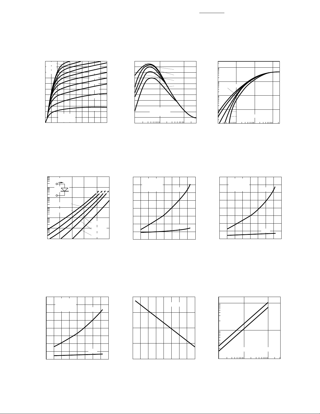
Figure 1. 6N138/6N139 DC Transfer
Characteristics.
1000
100
0.01
– FORWARD CURRENT – mA
F
I
0.001
I
F
+
V
F
–
10
TA = 85°C
1.0
TA = 70°C
0.1
1.1 1.2 1.3 1.4
VF – FORWARD VOLTAGE – V
TA = 25°C
TA = 0°C
TA = -40°C
85°C
2000
1600
1200
800
400
0
CTR – CURRENT TRANSFER RATIO – %
0.1 1.0
VCC = 5 V
= 0.4 V
V
O
IF – FORWARD CURRENT – mA
Figure 2. Current Transfer Ratio vs.
Forward Current 6N138/6N139.
40
IF = 0.5 mA
R
35
30
25
20
15
10
– PROPAGATION DELAY – µs
5
P
t
1.61.5
0
-60 -20
= 4.7 kΩ
L
1/f = 50 µs
-40
0
20 40
TA – TEMPERATURE – °C
70°C
25°C
70°C
-40°C
t
PLH
t
PHL
60 80
100
10
TA = 85° C
1.0
TA = 70° C
0.1
– OUTPUT CURRENT – mA
O
I
10
0.01
0.01 0.1 10
IF – INPUT DIODE FORWARD CURRENT – mA
TA = 25° C
TA = 0° C
TA = -40° C
1
Figure 3. 6N138/6N139 Output
Current vs. Input Diode Forward
Current.
24
IF = 1.6 mA
= 2.2 kΩ
R
21
18
15
12
– PROPAGATION DELAY – µs
P
t
100
L
1/f = 50 µs
9
6
3
0
-40
-60 -20
TA – TEMPERATURE – °C
0
20 40
t
PLH
t
PHL
60 80
100
Figure 4. Input Diode Forward
Current vs. Forward Voltage.
4
IF = 12 mA
= 270 kΩ
R
L
1/f = 50 µs
3
2
1
– PROPAGATION DELAY – µs
P
t
0
-40
-60 -20
0
TA – TEMPERATURE – °C
20 40
t
PLH
t
PHL
60 80
Figure 7. Propagation Delay vs.
Temperature.
Figure 5. Propagation Delay vs.
Temperature.
1.6
0
IF = 1.6 mA
20 40
60 80
100
1.5
1.4
1.3
– FORWARD VOLTAGE – V
F
V
1.2
-60 -20
-40
TA – TEMPERATURE – °C
Figure 8. Forward Voltage vs.
Temperature.
Figure 6. Propagation Delay vs.
Temperature.
100
T
= 25° C
A
10
TIME – µs
IF – ADJUSTED FOR V
1
100
0.1 1.0
RL – LOAD RESISTANCE – kΩ
Figure 9. Nonsaturated Rise and Fall
Times vs. Load Resistance.
t
f
t
r
= 2 V
OL
10
Page 14

14
0.8
0.7
0.6
0.5
0.4
0.3
0.2
0.1
– LOGIC LOW SUPPLY CURRENT – mA
0
04
CCL
I
V
= 18 V
CC
2
IF – FORWARD CURRENT
6
810
V
CC
12 14
= 5 V
Figure 10. Logic Low Supply Current
vs. Forward Current.
S
1000
900
800
WIDEBODY
PS (mW)
I
(mA)
S
700
600
, INPUT CURRENT – I
500
S
400
300
200
100
0
16
0
OUTPUT POWER – P
50
12525 75 100 150
TS – CASE TEMPERATURE – °C
175
Figure 11. Thermal Derating Curve,
Dependence of Safety Limiting Value
with Case Temperature per IEC/EN/DIN
EN 60747-5-2.
I
F
0
V
O
(SATURATED
RESPONSE)
t
PHL
V
O
(NON-SATURATED
RESPONSE)
t
f
1.5 V 1.5 V
90%
10%
10%
Figure 12. Switching Test Circuit.
90%
t
5 V
V
OL
PLH
5 V
t
r
PULSE
GEN.
Z = 50 Ω
O
t = 5 ns
r
10% DUTY CYCLE
I/f < 100 µs
I MONITOR
F
I
F
1
2
3
4
R
M
8
7
6
0.1 µF
5
* INCLUDES PROBE AND
FIXTURE CAPACITANCE
R
L
+5 V
V
O
C
= 15 pF*
L
Page 15

15
t
, tf = 16 ns
10%
r
t
f
10 V
V
CM
0 V
90% 90%
10%
t
r
I
F
1
B
A
2
3
V
O
SWITCH AT A: I = 0 mA
V
O
SWITCH AT B: I = 1.6 mA
F
F
5 V
V
OL
V
FF
4
Figure 13. Test Circuit for Transient Immunity and Typical Waveforms.
V
CM
+
–
PULSE GEN.
RCC(SEE NOTE 6)
8
7
6
5
+5 V
R
L
V
O
Page 16

www.agilent.com/semiconductors
For product information and a complete list of
distributors, please go to our web site.
For technical assistance call:
Americas/Canada: +1 (800) 235-0312 or
(916) 788-6763
Europe: +49 (0) 6441 92460
China: 10800 650 0017
Hong Kong: (+65) 6756 2394
India, Australia, New Zealand: (+65) 6755 1939
Japan: (+81 3) 3335-8152 (Domestic/Interna-
tional), or 0120-61-1280 (Domestic Only)
Korea: (+65) 6755 1989
Singapore, Malaysia, Vietnam, Thailand,
Philippines, Indonesia: (+65) 6755 2044
Taiwan: (+65) 6755 1843
Data subject to change.
Copyright © 2004 Agilent Technologies, Inc.
Obsoletes 5988-4109EN
January 22, 2004
5989-0289EN
 Loading...